US7243561B2 - Sensor device - Google Patents
Sensor deviceDownload PDFInfo
- Publication number
- US7243561B2 US7243561B2US10/531,074US53107405AUS7243561B2US 7243561 B2US7243561 B2US 7243561B2US 53107405 AUS53107405 AUS 53107405AUS 7243561 B2US7243561 B2US 7243561B2
- Authority
- US
- United States
- Prior art keywords
- lead
- physical
- signal
- molded body
- sensor
- Prior art date
- Legal status (The legal status is an assumption and is not a legal conclusion. Google has not performed a legal analysis and makes no representation as to the accuracy of the status listed.)
- Expired - Lifetime, expires
Links
- 230000001133accelerationEffects0.000claimsabstractdescription65
- 238000012545processingMethods0.000claimsabstractdescription61
- 230000009471actionEffects0.000claimsabstractdescription10
- 239000000463materialSubstances0.000claimsdescription12
- 238000000034methodMethods0.000claimsdescription7
- 230000008569processEffects0.000claimsdescription6
- 238000004891communicationMethods0.000claimsdescription4
- 239000012530fluidSubstances0.000claimsdescription4
- 229920005989resinPolymers0.000claimsdescription3
- 239000011347resinSubstances0.000claimsdescription3
- 229920002050silicone resinPolymers0.000description8
- 229910001030Iron–nickel alloyInorganic materials0.000description5
- 238000005259measurementMethods0.000description4
- 239000002184metalSubstances0.000description4
- 229910052751metalInorganic materials0.000description4
- 239000002245particleSubstances0.000description4
- 230000008646thermal stressEffects0.000description4
- 230000002411adverseEffects0.000description3
- 150000001875compoundsChemical class0.000description3
- 230000035882stressEffects0.000description3
- 238000005452bendingMethods0.000description2
- 239000000428dustSubstances0.000description2
- 230000004044responseEffects0.000description2
- 230000035939shockEffects0.000description2
- 230000004075alterationEffects0.000description1
- 230000008859changeEffects0.000description1
- 238000001514detection methodMethods0.000description1
- 230000000694effectsEffects0.000description1
- 239000007769metal materialSubstances0.000description1
- 238000012986modificationMethods0.000description1
- 230000004048modificationEffects0.000description1
- 238000000465mouldingMethods0.000description1
- 230000000704physical effectEffects0.000description1
- 238000005476solderingMethods0.000description1
Images


Classifications
- B—PERFORMING OPERATIONS; TRANSPORTING
- B60—VEHICLES IN GENERAL
- B60C—VEHICLE TYRES; TYRE INFLATION; TYRE CHANGING; CONNECTING VALVES TO INFLATABLE ELASTIC BODIES IN GENERAL; DEVICES OR ARRANGEMENTS RELATED TO TYRES
- B60C23/00—Devices for measuring, signalling, controlling, or distributing tyre pressure or temperature, specially adapted for mounting on vehicles; Arrangement of tyre inflating devices on vehicles, e.g. of pumps or of tanks; Tyre cooling arrangements
- B60C23/02—Signalling devices actuated by tyre pressure
- B60C23/04—Signalling devices actuated by tyre pressure mounted on the wheel or tyre
- B60C23/0408—Signalling devices actuated by tyre pressure mounted on the wheel or tyre transmitting the signals by non-mechanical means from the wheel or tyre to a vehicle body mounted receiver
- G—PHYSICS
- G01—MEASURING; TESTING
- G01L—MEASURING FORCE, STRESS, TORQUE, WORK, MECHANICAL POWER, MECHANICAL EFFICIENCY, OR FLUID PRESSURE
- G01L19/00—Details of, or accessories for, apparatus for measuring steady or quasi-steady pressure of a fluent medium insofar as such details or accessories are not special to particular types of pressure gauges
- G01L19/14—Housings
- G—PHYSICS
- G01—MEASURING; TESTING
- G01D—MEASURING NOT SPECIALLY ADAPTED FOR A SPECIFIC VARIABLE; ARRANGEMENTS FOR MEASURING TWO OR MORE VARIABLES NOT COVERED IN A SINGLE OTHER SUBCLASS; TARIFF METERING APPARATUS; MEASURING OR TESTING NOT OTHERWISE PROVIDED FOR
- G01D21/00—Measuring or testing not otherwise provided for
- G01D21/02—Measuring two or more variables by means not covered by a single other subclass
- G—PHYSICS
- G01—MEASURING; TESTING
- G01L—MEASURING FORCE, STRESS, TORQUE, WORK, MECHANICAL POWER, MECHANICAL EFFICIENCY, OR FLUID PRESSURE
- G01L19/00—Details of, or accessories for, apparatus for measuring steady or quasi-steady pressure of a fluent medium insofar as such details or accessories are not special to particular types of pressure gauges
- G01L19/0061—Electrical connection means
- G01L19/0084—Electrical connection means to the outside of the housing
- G—PHYSICS
- G01—MEASURING; TESTING
- G01L—MEASURING FORCE, STRESS, TORQUE, WORK, MECHANICAL POWER, MECHANICAL EFFICIENCY, OR FLUID PRESSURE
- G01L19/00—Details of, or accessories for, apparatus for measuring steady or quasi-steady pressure of a fluent medium insofar as such details or accessories are not special to particular types of pressure gauges
- G01L19/0092—Pressure sensor associated with other sensors, e.g. for measuring acceleration or temperature
- G—PHYSICS
- G01—MEASURING; TESTING
- G01L—MEASURING FORCE, STRESS, TORQUE, WORK, MECHANICAL POWER, MECHANICAL EFFICIENCY, OR FLUID PRESSURE
- G01L19/00—Details of, or accessories for, apparatus for measuring steady or quasi-steady pressure of a fluent medium insofar as such details or accessories are not special to particular types of pressure gauges
- G01L19/14—Housings
- G01L19/141—Monolithic housings, e.g. molded or one-piece housings
- G—PHYSICS
- G01—MEASURING; TESTING
- G01L—MEASURING FORCE, STRESS, TORQUE, WORK, MECHANICAL POWER, MECHANICAL EFFICIENCY, OR FLUID PRESSURE
- G01L19/00—Details of, or accessories for, apparatus for measuring steady or quasi-steady pressure of a fluent medium insofar as such details or accessories are not special to particular types of pressure gauges
- G01L19/14—Housings
- G01L19/148—Details about the circuit board integration, e.g. integrated with the diaphragm surface or encapsulation
- G—PHYSICS
- G01—MEASURING; TESTING
- G01P—MEASURING LINEAR OR ANGULAR SPEED, ACCELERATION, DECELERATION, OR SHOCK; INDICATING PRESENCE, ABSENCE, OR DIRECTION, OF MOVEMENT
- G01P1/00—Details of instruments
- G01P1/02—Housings
- G—PHYSICS
- G01—MEASURING; TESTING
- G01P—MEASURING LINEAR OR ANGULAR SPEED, ACCELERATION, DECELERATION, OR SHOCK; INDICATING PRESENCE, ABSENCE, OR DIRECTION, OF MOVEMENT
- G01P1/00—Details of instruments
- G01P1/02—Housings
- G01P1/023—Housings for acceleration measuring devices
- H—ELECTRICITY
- H01—ELECTRIC ELEMENTS
- H01L—SEMICONDUCTOR DEVICES NOT COVERED BY CLASS H10
- H01L2224/00—Indexing scheme for arrangements for connecting or disconnecting semiconductor or solid-state bodies and methods related thereto as covered by H01L24/00
- H01L2224/01—Means for bonding being attached to, or being formed on, the surface to be connected, e.g. chip-to-package, die-attach, "first-level" interconnects; Manufacturing methods related thereto
- H01L2224/42—Wire connectors; Manufacturing methods related thereto
- H01L2224/47—Structure, shape, material or disposition of the wire connectors after the connecting process
- H01L2224/48—Structure, shape, material or disposition of the wire connectors after the connecting process of an individual wire connector
- H01L2224/4805—Shape
- H01L2224/4809—Loop shape
- H01L2224/48091—Arched
- H—ELECTRICITY
- H01—ELECTRIC ELEMENTS
- H01L—SEMICONDUCTOR DEVICES NOT COVERED BY CLASS H10
- H01L2224/00—Indexing scheme for arrangements for connecting or disconnecting semiconductor or solid-state bodies and methods related thereto as covered by H01L24/00
- H01L2224/01—Means for bonding being attached to, or being formed on, the surface to be connected, e.g. chip-to-package, die-attach, "first-level" interconnects; Manufacturing methods related thereto
- H01L2224/42—Wire connectors; Manufacturing methods related thereto
- H01L2224/47—Structure, shape, material or disposition of the wire connectors after the connecting process
- H01L2224/48—Structure, shape, material or disposition of the wire connectors after the connecting process of an individual wire connector
- H01L2224/481—Disposition
- H01L2224/48151—Connecting between a semiconductor or solid-state body and an item not being a semiconductor or solid-state body, e.g. chip-to-substrate, chip-to-passive
- H01L2224/48221—Connecting between a semiconductor or solid-state body and an item not being a semiconductor or solid-state body, e.g. chip-to-substrate, chip-to-passive the body and the item being stacked
- H01L2224/48245—Connecting between a semiconductor or solid-state body and an item not being a semiconductor or solid-state body, e.g. chip-to-substrate, chip-to-passive the body and the item being stacked the item being metallic
- H01L2224/48247—Connecting between a semiconductor or solid-state body and an item not being a semiconductor or solid-state body, e.g. chip-to-substrate, chip-to-passive the body and the item being stacked the item being metallic connecting the wire to a bond pad of the item
- H—ELECTRICITY
- H01—ELECTRIC ELEMENTS
- H01L—SEMICONDUCTOR DEVICES NOT COVERED BY CLASS H10
- H01L2224/00—Indexing scheme for arrangements for connecting or disconnecting semiconductor or solid-state bodies and methods related thereto as covered by H01L24/00
- H01L2224/01—Means for bonding being attached to, or being formed on, the surface to be connected, e.g. chip-to-package, die-attach, "first-level" interconnects; Manufacturing methods related thereto
- H01L2224/42—Wire connectors; Manufacturing methods related thereto
- H01L2224/47—Structure, shape, material or disposition of the wire connectors after the connecting process
- H01L2224/49—Structure, shape, material or disposition of the wire connectors after the connecting process of a plurality of wire connectors
- H01L2224/491—Disposition
- H01L2224/4912—Layout
- H01L2224/49171—Fan-out arrangements
- H—ELECTRICITY
- H01—ELECTRIC ELEMENTS
- H01L—SEMICONDUCTOR DEVICES NOT COVERED BY CLASS H10
- H01L2224/00—Indexing scheme for arrangements for connecting or disconnecting semiconductor or solid-state bodies and methods related thereto as covered by H01L24/00
- H01L2224/73—Means for bonding being of different types provided for in two or more of groups H01L2224/10, H01L2224/18, H01L2224/26, H01L2224/34, H01L2224/42, H01L2224/50, H01L2224/63, H01L2224/71
- H01L2224/732—Location after the connecting process
- H01L2224/73251—Location after the connecting process on different surfaces
- H01L2224/73265—Layer and wire connectors
- H—ELECTRICITY
- H01—ELECTRIC ELEMENTS
- H01L—SEMICONDUCTOR DEVICES NOT COVERED BY CLASS H10
- H01L2924/00—Indexing scheme for arrangements or methods for connecting or disconnecting semiconductor or solid-state bodies as covered by H01L24/00
- H01L2924/15—Details of package parts other than the semiconductor or other solid state devices to be connected
- H01L2924/181—Encapsulation
- H01L2924/1815—Shape
Definitions
- the present inventionrelates to a sensor unit for measuring a plurality of physical quantities.
- a plurality of separately-packaged sensorshave been used.
- the plurality of separately-packaged sensorshave to be mounted on a circuit board individually. This involves the need for assuring a large space (area) for mounting these physical-quantity sensors in the circuit board, which leads to undesirable increases in size, complexity and cost of the measuring system.
- Patent Publication 1discloses a compound sensor unit having a pressure sensor for detecting a pressure and a temperature sensor for detecting a temperature which are incorporated into a single package.
- Patent Publication 1Japanese Patent No. 3149957 (FIG. 2)
- a conventional compound sensor unit as disclosed, for example, in Patent Publication 1can solve the above problem caused by mounting a plurality of sensors on a circuit board individually.
- the conventional compound sensor unitinvolves a problem concerning higher power consumption because it is designed to drive the pressure sensor and the temperature sensor independently.
- a sensor-driving battery to be equipped in a measuring systemis required to have a larger capacity.
- the present inventionprovides a sensor unit including a lead, a plurality of physical-quantity sensors, a signal-processing circuit and a molded body.
- the leadhas edges formed as lead terminals serving as input/output terminals.
- Each of the physical-quantity sensorsis disposed relative to the lead and adapted to measure a physical quantity.
- the signal-processing circuitis disposed relative to the lead and adapted to process a signal from each of the physical-quantity sensors.
- the molded bodyis made of a plastic material, and formed to seal the lead, the physical-quantity sensors and the signal-processing circuit in such a manner as to allow the lead terminals to protrude outside the molded body.
- the signal-processing circuitis operable, based on the signal from at least one of the plurality of physical-quantity sensors, to control the ON/OFF action of the remaining physical-quantity sensors.
- the space (area) required for mounting the physical-quantity sensorscan be reduced.
- the signal-processing circuitis operable, based on the signal from at least one of the physical-quantity sensors, to control the ON/OFF action of the remaining physical-quantity sensors, so that the need for constantly driving all of the physical-quantity sensors can be eliminated to achieve lower power consumption.
- the plurality of physical-quantity sensorsinclude a pressure sensor and an acceleration sensor.
- the molded bodyis formed with a through-hole extending upward from a pressure-receiving portion of the pressure sensor and having an opening to the outside of the molded body. This through-hole defines a pressure-introducing passage which allows fluid communication between the outside of the molded body and the pressure-receiving portion.
- the plurality of physical-quantity sensorsmay include an acceleration sensor and a rotational-angular-velocity sensor.
- the pressure sensor, the acceleration sensor and the signal-processing circuitare disposed to form a line in the longitudinal direction of the sensor unit.
- the pressure sensor and the acceleration sensormay be disposed at respective symmetrical positions with respect to the center of the signal-processing circuit in the longitudinal direction of the sensor unit.
- each of the pressure sensor and the acceleration sensormay have substantially the same height dimension. According to this pressure/acceleration sensor, the respective thicknesses of the molded body on the underside of the pressure sensor and on the underside of the acceleration sensor are substantially equalized so that respective stresses on the longitudinal opposite ends of the sensor unit are balanced. This provides enhanced measurement accuracy.
- the pressure/acceleration sensorincludes a flexible resin interposed between the acceleration sensor and the molded body.
- the resincan suppress the deformation of the acceleration sensor to provide enhanced measurement accuracy.
- the pressure-introducing passagemay include a plurality of small-diameter channels. This can prevent foreign matter, such as foreign particles or dust, from getting into the pressure sensor. In addition, even if an excessive pressure is introduced into the through-hole, the channels can reduce the shock due to the pressure to prevent breakage of the pressure sensor.
- the molded bodymay be integrally formed with a tubular portion extending continuously from the edge of the opening of the through-hole to the outside of the molded body and having substantially the same inner diameter as that of the through-hole.
- the tubular portioncan prevent the silicone resin or the like from getting into the pressure-introducing passage.
- the tubular portioncan also prevent foreign matter, such as foreign particles or dust, from getting into the pressure-introducing passage.
- each of the plurality of physical-quantity sensorsmay have substantially the same height dimension.
- the molded bodyhas a first portion extending between each of the physical-quantity sensors and an outer surface of the molded body on the side of the physical quantity sensor and a second portion extending between the lead and an outer surface of the molded body on the side of the lead, wherein each of the first and second portions has substantially the same thickness dimension.
- the molded bodymay have a first portion covering the top-surface side of the lead and a second portion covering the bottom-surface side of the lead, and the first and second portions may be formed to have different tapered shapes from one another so as to allow the respective volumes of the first and second portions to be substantially equalized. This can reduce a thermal stress caused by the difference in linear expansion coefficient between the lead and the molded body made of a plastic material, to achieve a reduced temperature dependence of the sensor unit.
- At least one of the plurality of physical-quantity sensors and the signal-processing circuitmay be disposed, respectively, on the top and bottom surfaces of the lead in such a manner as to sandwich the lead therebetween.
- the lead made of metalsuch as iron-nickel alloy, is interposed between ICs of the signal-processing circuit and the physical-quantity sensor.
- the leadcan prevent the physical-quantity sensor from being adversely affected by noises generated from the signal-processing circuit.
- FIG. 1is a top plan view of a sensor unit according to a first embodiment of the present invention.
- FIG. 2is a sectional view of the sensor unit in FIG. 1 , taken along the line A-A.
- FIG. 3is a partial sectional view of the sensor unit in FIG. 1 , taken along the line B-B.
- FIG. 4is a bottom view of the sensor unit in FIG. 1 .
- FIG. 5is a bottom view showing an internal wiring of the sensor unit in FIG. 1 , wherein a lower molded body is removed therefrom.
- FIG. 6is a top plan view of a sensor unit according to a second embodiment of the present invention.
- FIG. 7is a vertical sectional view of the sensor unit in FIG. 6 .
- FIG. 8is a bottom view showing an internal wiring of the sensor unit in FIG. 6 , wherein a molded body is removed therefrom.
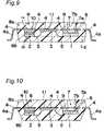
- FIG. 9is a vertical sectional view of a sensor unit according to a third embodiment of the present invention.
- FIG. 10is a sectional view of a sensor unit according to a fourth embodiment of the present invention.
- FIG. 11is a top plan view of a sensor unit according to a fifth embodiment of the present invention.
- FIG. 12is a vertical sectional view of the sensor unit in FIG. 11 .
- FIG. 13is a top plan view of a sensor unit according to a sixth embodiment of the present invention.
- FIG. 14is a vertical sectional view of the sensor unit in FIG. 13 .
- FIG. 15is a vertical sectional view of a sensor unit according to a seventh embodiment of the present invention.
- FIG. 16is a vertical sectional view of a sensor unit according to an eighth embodiment of the present invention.
- a sensor unit of the present inventionmay be used, for example, as a tire-air-pressure sensor.
- a sensor unit according to a first embodiment of the present inventionincludes a pressure sensor 1 , an acceleration sensor 2 and a signal-processing circuit (signal processing IC) 3 .
- the signal-processing circuit 3is operable, only when the acceleration sensor 2 detects acceleration, to activate the pressure sensor 1 .
- Each of the pressure sensor 1 , the acceleration sensor 2 and the signal-processing circuit 3is mounted on the bottom surface of a lead 4 .
- the signal-processing circuit 3is wire-bonded or electrically connected to each of the pressure sensor 1 and the acceleration sensor 2 through a plurality of bonding wires 5 .
- a portion of the lead 4 mounting the pressure sensor 1is formed with one opening 7 a for transmitting an external pressure to a pressure-receiving portion 6 formed in the pressure sensor 1 .
- the pressure-receiving portion 6is composed, for example, of a diaphragm, and operable to detect a pressure.
- the lead 4is covered and sealed with a molded body 8 made of a plastic material, in such a manner as to allow a plurality of lead terminals 4 a to protrude outside the molded body 8 .
- the molded body 8consists of an upper molded body 8 a located on the side of the top surface of the lead 4 , and a lower molded body 8 b located on the side of the bottom surface of the lead 4 .
- the upper molded body 8 ahas a through-hole 7 b for allowing the opening 7 a to be exposed to the outside of the molded body 8 .
- the opening 7 a and the through-hole 7 bare in fluid communication with one another to define a pressure-introducing passage 7 for transmitting an external pressure to the pressure-receiving portion 6 .
- a flexible silicone resin 15is disposed between the bottom surface of the acceleration sensor 2 and the lower molded body 8 b . This silicone resin 15 suppresses the deformation of the acceleration sensor 2 due to pressure.
- the lead 4is prepared by cutting and removing a part of a lead frame made of metal, such as iron-nickel alloy.
- the lead 4has a rectangular-shaped pressure-sensor mounting portion 9 for mounting the pressure sensor 1 , a rectangular-shaped acceleration-sensor mounting portion 10 for mounting the acceleration sensor 2 , a rectangular-shaped signal-processing circuit mounting portion 11 for mounting the signal-processing circuit 3 , and the lead terminals 4 a .
- the pressure-sensor mounting portion 9 , the signal-processing circuit mounting portion 11 and the acceleration-sensor mounting portion 10are integrally formed as a single piece in such a manner that they are disposed to form a line in the longitudinal direction of the sensor unit (right-left direction in FIGS. 4 and 5 ).
- Each of the pressure-sensor mounting portion 9 and the acceleration-sensor mounting portion 10is integrally formed with two or more of the lead terminals 4 a which protrude outward in the lengthwise (longitudinal) direction of the sensor unit.
- the sensor unitis also provided with a plurality of leads 4 ′ which are formed separately from the lead 4 and electrically connected or wire-bonded to the signal-processing circuit 3 through bonding wires 5 .
- Each of the leads 41has a lead terminal 4 a .
- the lead terminals 4 a of the leads 4 ′protrude from the molded body 8 parallel to each other in the crosswise direction of the sensor unit (a direction perpendicular to the longitudinal direction of the sensor unit).
- the pressure-sensor mounting portion 9 , the signal-processing circuit mounting portion 11 and the acceleration-sensor mounting portion 10are disposed to form a line in the longitudinal direction of the sensor unit. Further, in the positional relationship in the longitudinal direction of the sensor unit, the pressure-sensor mounting portion 9 and the acceleration-sensor mounting portion 10 are disposed at respective symmetrical positions with respect to the center of the signal-processing circuit mounting portion 11 . Furthermore, the height dimension or thickness h 1 of the pressure sensor 1 is set to be substantially equal to the height dimension or thickness h 2 of the acceleration sensor 2 .
- both the pressure sensor 1 and the acceleration sensor 2are mounted on the bottom surface of the lead 4 , and thereby the respective bottom surfaces of these sensors 1 , 2 are located at substantially the same height position. This allows the respective thicknesses of the lower molded body 8 b on the underside of the pressure sensor 1 and on the underside of the acceleration sensor 2 to be substantially equalized. Thus, respective stresses on the longitudinal opposite ends of the sensor unit can be balanced.
- the pressure sensor 1 and the acceleration sensor 2are integrally mounted on the lead 4 , and sealed with the molded body 8 .
- a required mounting space (area) on a circuit boardcan be reduced.
- the signal-processing circuit 3 operable to control the ON/OFF action of the pressure sensor 1 in response to a signal from the acceleration sensor 2can achieve lower power consumption.
- the batterycan be reduced in size.
- the deformation of the acceleration sensor 2is suppressed by the silicone resin 15 , and the respective stresses on the longitudinal opposite ends of the sensor unit is balanced, so that the measurement accuracy of the sensor unit can be drastically improved.
- a sensor unitincludes a pressure sensor 1 , an acceleration sensor 2 , and a signal-processing circuit (signal processing IC) 3 having a function designed to activate the pressure sensor 1 only when the acceleration sensor 2 detects acceleration.
- a signal-processing circuitsignal processing IC 3 having a function designed to activate the pressure sensor 1 only when the acceleration sensor 2 detects acceleration.
- Each of the pressure sensor 1 , the acceleration sensor 2 and the signal-processing circuit 3is mounted on the bottom surface of a lead 4 .
- the signal-processing circuit 3is wire-bonded or electrically connected to each of the pressure sensor 1 and the acceleration sensor 2 through two bonding wires 5 .
- a portion of the lead 4 mounting the pressure sensor 1is formed with one opening 7 a for transmitting an external pressure to a pressure-receiving portion 6 formed in the pressure sensor 1 .
- the pressure-receiving portion 6is composed, for example, of a diaphragm, and operable to detect a pressure.
- the lead 4is covered and sealed with a molded body 8 made of a plastic material, in such a manner as to allow a plurality of lead terminals 4 a to protrude outside the molded body 8 .
- the molded body 8consists of an upper molded body 8 a located on the side of the top surface of the lead 4 , and a lower molded body 8 b located on the side of the bottom surface of the lead 4 .
- the upper molded body 8 ahas a through-hole 7 b for allowing the opening 7 a to be exposed to the outside of the molded body 8 .
- the opening 7 a and the through-hole 7 bare in fluid communication with one another to define a pressure-introducing passage 7 . An external pressure is transmitted to the pressure-receiving portion 6 through the pressure-introducing passage 7 .
- FIG. 8shows the sensor unit in the state before the lead 4 is sealed with the molded body 8 .
- the dotted line L 1 in FIG. 8indicates a region in which the molded body 8 is to be formed.
- the lead 4is prepared by cutting and removing a part of a lead frame made of metal, such as iron-nickel alloy.
- the lead 4has a rectangular-shaped pressure-sensor mounting portion 9 for mounting the pressure sensor 1 , a rectangular-shaped acceleration-sensor mounting portion 10 for mounting the acceleration sensor 2 , a rectangular-shaped signal-processing-circuit mounting portion 11 for mounting the signal-processing circuit 3 , and the lead terminals 4 a .
- the lead 4is integrally formed as a single piece in such a manner that one of two diagonally-opposed corners of the signal-processing circuit mounting portion 11 is joined to one corner of the pressure-sensor mounting portion 9 , and the other corner of the signal-processing-circuit mounting portion 11 is joined to one corner of the acceleration-sensor mounting portion 10 .
- Each of the outer corners of the pressure-sensor mounting portion 9 and the acceleration-sensor mounting portion 10is integrally formed with the lead terminals 4 a protruding outward.
- the sensor unitis also provided with a plurality of leads 4 ′ which are formed separately from the lead 4 . These leads 4 ′ are electrically connected or wire-bonded to the signal-processing circuit 3 through bonding wires 5 .
- the leads 4 ′are disposed to extend outward from the vicinity of the outer periphery of the signal-processing circuit 3 in a radial pattern.
- Lead terminals 4 a of the leads 4 ′protrude outward from the molded body 8 parallel to each other in the lengthwise and crosswise directions of the sensor unit.
- the lead terminals protruding from the molded body 8are used as input/output terminals. Further, the molded body 8 is provided with one dummy lead terminal 4 a ′ having no function.
- the pressure sensor 1 and the acceleration sensor 2are integrally mounted on the lead 4 , and sealed with the molded body 8 .
- a required mounting area on a circuit boardcan be reduced.
- the signal-processing circuit 3 operable to control the ON/OFF action of the pressure sensor 1 in response to a signal from the acceleration sensor 2can achieve lower power consumption.
- the batterycan be reduced in size.
- the sensor unit according to the second embodimentemploys a combination of a pressure sensor and an acceleration sensor
- any other combination of sensorsmay be used.
- an acceleration sensor and a rotational-angular-velocity sensormay be combined, and the signal-processing circuit may be designed to activate the acceleration sensor only when the rotational-angular-velocity sensor detects rotational angular velocity.
- This sensor unitcan be used, for example, in a vehicle, such as automobile, to detect a lateral acceleration relative to a traveling direction only when a steering wheel is turned to change the traveling direction. It is to be understood that any other physical-quantity sensor may be additionally incorporated in the sensor unit within the spirit and scope of the present invention.
- each of a pressure sensor 1 and an acceleration sensor 2has substantially the same height dimension or thickness. That is, the respective bottom surfaces of the pressure sensor 1 and the acceleration sensor 2 are located at substantially the same height position indicated by the dotted line L 2 .
- an upper molded body 8 a and a lower molded body 8 bare formed such that the height dimension ta (thickness) between the top surface of the upper molded body 8 a and the top surface of a lead 4 becomes substantially equal to the height dimension tb (thickness) between the bottom surface of the lower molded body 8 b and each of the bottom surfaces of the pressure sensor 1 and the acceleration sensor 2 .
- the remaining structuresare the same as those in the second embodiment, and their description will be omitted.
- each of the pressure sensor 1 and the acceleration sensor 2has substantially the same thickness, and the respective thicknesses of the molded body 8 on the top-surface side and the bottom-surface side thereof are substantially equalized at the positions corresponding to the pressure sensor 1 and the acceleration sensor 2 .
- Thiscan reduce a thermal stress caused by the difference in linear expansion coefficient between each physical-quantity sensor (sensor element), such as the pressure sensor 1 and the acceleration sensor 2 , and the molded body 8 made of a plastic material, to achieve a reduced temperature dependence of the sensor unit.
- the above characteristic structure in the sensor unit according to the third embodimentmay be applied to each of the aforementioned first and second embodiments and after-mentioned fourth to eighth embodiments.
- a molded body 8consists of an upper molded body 8 a located on the upper side relative to a lead 4 and a lower molded body 8 b located on the lower side relative to the lead 4 , and the upper molded body 8 a and the lower molded body 8 b are formed to have different tapered shapes from one another so as to allow the respective volumes of the upper and lower molded bodies 8 a , 8 b to be substantially equalized.
- the remaining structuresare the same as those in the second embodiment, and their description will be omitted.
- each of the upper molded body 8 a and the lower molded body 8 bhas substantially the same volume. This can reduce a thermal stress caused by the difference in linear expansion coefficient between a metal material, such as iron-nickel alloy, constituting the lead 4 , and a plastic material constituting the molded body 8 , to achieve a reduced temperature dependence of the sensor unit.
- the above characteristic structure in the sensor unit according to the fourth embodimentmay be applied to each of the aforementioned first to third embodiments and after-mentioned fifth to eighth embodiments.
- a fifth embodiment of the present inventionwill be specifically described below.
- a tubular portion 12having substantially the same inner diameter as that of a through-hole 7 b , or a tubular protrusion, is integrally formed in a molded body 8 through a molding method in such a manner as to extend a pressure-introducing passage 7 .
- the remaining structuresare the same as those in the second embodiment, and their description will be omitted.
- the tubular portion 12is integrally formed with the molded body 8 to extend the pressure-introducing passage 7 .
- the tubular portion 12can prevent the silicone resin or the like from getting into the pressure-introducing passage 7 .
- the tubular portion 12can also prevent foreign matter, such as foreign particles or dusts, from getting into the pressure-introducing passage 7 .
- a sixth embodiment of the present inventionwill be specifically described below.
- a pressure-sensor mounting portion 9 of a lead 4is formed with four small-diameter channels 7 c for transmitting an external pressure to a pressure-receiving portion 6 .
- these small-diameter channels 7 c and a through-hole 7 b formed in an upper molded body 8 bdefine four pressure-introducing passages 7 .
- the remaining structuresare the same as those in the second embodiment, and their description will be omitted.
- the four small-diameter channels 7 c or pressure-introducing passages 7 each having a small diametercan prevent foreign matter, such as foreign particles or dusts, from getting into a pressure sensor 1 through the pressure-introducing passages 7 .
- the four pressure-introducing passages 7 each having a small diameterreduces the shock due to the pressure. This can prevent breakage of the pressure sensor due to the excessive pressure.
- the number of the small-diameter channels 7 cis not limited to four. That is, any plural number of small-diameter channels 7 c or pressure-introducing passages 7 may be formed to obtain the same effect. Further, a plurality of pressure-introducing passages 7 may be defined by combining a plurality of small-diameter channels 7 c with a plurality of independent through-holes 7 b -formed relative to the respective small-diameter channels 7 c .
- the above characteristic structure in the sensor unit according to the sixth embodimentmay be applied to the aforementioned fifth embodiment.
- each of a plurality of lead terminals 4 ahas an edge formed as a joint surface 4 b to be soldered to a circuit board 13 consisting of a printed board.
- the joint surface 4 b and the bottom surface of a molded body 8are spaced apart from one another by a given distance vertically (in the thickness direction of the molded body 8 ).
- the joint surface 4 bis formed by bending the lead terminal 4 a in a direction parallel to the side surface of the molded body 8 and then bending the edge of the bended lead terminal 4 a outward relative to the molded body 8 and in a direction parallel to the bottom surface of the molded body 8 .
- Each of the joint surfaces 4 ais joined to the circuit board 13 through soldering.
- the remaining structuresare the same as those in the second embodiment, and their description will be omitted.
- each of the joint surfaces 4 ais formed to have a given distance relative to the bottom surface of the molded body 8 . This prevents the contact between a lower molded body 8 b and the circuit board 13 during an operation of joining the sensor unit to the circuit board 13 . That is, only the joint surfaces 4 b are brought into contact with and soldered to the circuit board 13 . Thus, even if the circuit board 13 is deformed, adverse affects due to the deformation can be suppressed.
- the above characteristic structure in the sensor unit according to the seventh embodimentmay be applied to each of the aforementioned first to sixth embodiments and an after-mentioned eighth embodiment.
- a lead 4has a pressure-sensor mounting portion 9 , and a device mounting portion. 14 formed by integrating an acceleration-sensor mounting portion and a signal-processing-circuit mounting portion.
- a signal-processing circuit 3is disposed on the top surface of the device mounting portion 14
- an acceleration sensor 2is disposed on the bottom surface of the device mounting portion 14 . That is, the device mounting portion 14 of the lead 4 is sandwiched between the signal-processing circuit 3 and the acceleration sensor 2 .
- the remaining structuresare the same as those in the second embodiment, and their description will be omitted.
- the signal-processing circuit 3 and the acceleration sensor 2are disposed on the top and bottom surfaces of the lead 4 , respectively. This allows the sensor unit to be reduced in size.
- the lead 4 made of metal, such as iron-nickel alloy,is interposed between the signal-processing circuit 3 and the acceleration sensor 2 .
- the lead 4can prevent the acceleration sensor 2 from being adversely affected by noises of the signal-processing circuit 3 .
- the above characteristic structure in the sensor unit according to the eighth embodimentmay be applied to each of the aforementioned second to seventh embodiments.
- the sensor unit of the present inventionis useful, particularly, to the measurement of a plurality of physical quantities, and suitable for use as a sensor for detecting a plurality of physical quantities, such as a tire-air-pressure sensor for measuring pressure and acceleration.
Landscapes
- Physics & Mathematics (AREA)
- General Physics & Mathematics (AREA)
- Chemical & Material Sciences (AREA)
- Analytical Chemistry (AREA)
- Engineering & Computer Science (AREA)
- Mechanical Engineering (AREA)
- Measuring Fluid Pressure (AREA)
- Pressure Sensors (AREA)
Abstract
Description
Claims (13)
Applications Claiming Priority (3)
| Application Number | Priority Date | Filing Date | Title |
|---|---|---|---|
| JP2003-301907 | 2003-08-26 | ||
| JP2003301907 | 2003-08-26 | ||
| PCT/JP2004/012270WO2005019790A1 (en) | 2003-08-26 | 2004-08-26 | Sensor device |
Publications (2)
| Publication Number | Publication Date |
|---|---|
| US20060053908A1 US20060053908A1 (en) | 2006-03-16 |
| US7243561B2true US7243561B2 (en) | 2007-07-17 |
Family
ID=34213917
Family Applications (1)
| Application Number | Title | Priority Date | Filing Date |
|---|---|---|---|
| US10/531,074Expired - LifetimeUS7243561B2 (en) | 2003-08-26 | 2004-08-26 | Sensor device |
Country Status (6)
| Country | Link |
|---|---|
| US (1) | US7243561B2 (en) |
| EP (1) | EP1659386A4 (en) |
| JP (1) | JPWO2005019790A1 (en) |
| KR (1) | KR20050059273A (en) |
| CN (1) | CN100381804C (en) |
| WO (1) | WO2005019790A1 (en) |
Cited By (21)
| Publication number | Priority date | Publication date | Assignee | Title |
|---|---|---|---|---|
| US20070126130A1 (en)* | 2005-11-14 | 2007-06-07 | Alfons Dehe | Sensor Module And Method For Manufacturing Same |
| US20080314147A1 (en)* | 2007-06-21 | 2008-12-25 | Invensense Inc. | Vertically integrated 3-axis mems accelerometer with electronics |
| US20090007661A1 (en)* | 2007-07-06 | 2009-01-08 | Invensense Inc. | Integrated Motion Processing Unit (MPU) With MEMS Inertial Sensing And Embedded Digital Electronics |
| US20090013784A1 (en)* | 2006-03-17 | 2009-01-15 | Matsushita Electric Industrial Co., Ltd. | Composite sensor |
| US20090049921A1 (en)* | 2007-08-20 | 2009-02-26 | Denso Corporation | Pressure sensor and method for manufacturing the same |
| US20090145225A1 (en)* | 2007-12-10 | 2009-06-11 | Invensense Inc. | Vertically integrated 3-axis MEMS angular accelerometer with integrated electronics |
| US20090184849A1 (en)* | 2008-01-18 | 2009-07-23 | Invensense, Inc. | Interfacing application programs and motion sensors of a device |
| US20090193892A1 (en)* | 2008-02-05 | 2009-08-06 | Invensense Inc. | Dual mode sensing for vibratory gyroscope |
| US20090265671A1 (en)* | 2008-04-21 | 2009-10-22 | Invensense | Mobile devices with motion gesture recognition |
| US20090303204A1 (en)* | 2007-01-05 | 2009-12-10 | Invensense Inc. | Controlling and accessing content using motion processing on mobile devices |
| US20100064805A1 (en)* | 2008-09-12 | 2010-03-18 | InvenSense,. Inc. | Low inertia frame for detecting coriolis acceleration |
| US20100071467A1 (en)* | 2008-09-24 | 2010-03-25 | Invensense | Integrated multiaxis motion sensor |
| US20100154540A1 (en)* | 2008-12-19 | 2010-06-24 | Panasonic Corporation | Sensor device |
| US20100206075A1 (en)* | 2009-02-17 | 2010-08-19 | Seiko Epson Corporation | Composite sensor and electronic device |
| US20100242603A1 (en)* | 2009-03-24 | 2010-09-30 | Freescale Semiconductor, Inc. | Vertically integrated mems sensor device with multi-stimulus sensing |
| US20120000285A1 (en)* | 2009-03-31 | 2012-01-05 | Satoshi Waga | Capacitive type humidity sensor and manufacturing method thereof |
| US8508039B1 (en) | 2008-05-08 | 2013-08-13 | Invensense, Inc. | Wafer scale chip scale packaging of vertically integrated MEMS sensors with electronics |
| US20150370310A1 (en)* | 2013-02-08 | 2015-12-24 | Panasonic Intellectual Property Management Co., Ltd. | Electronic device |
| US9266717B2 (en) | 2013-03-15 | 2016-02-23 | Versana Micro Inc | Monolithically integrated multi-sensor device on a semiconductor substrate and method therefor |
| US9961779B2 (en) | 2012-12-20 | 2018-05-01 | Continental Teves Ag & Co. Ohg | Method for producing an electronic assembly |
| US11105629B2 (en)* | 2018-06-13 | 2021-08-31 | Seiko Epson Corporation | Physical quantity sensor, composite sensor, inertial measurement unit, vehicle positioning device, portable electronic device, electronic device, vehicle, traveling supporting system, and display device |
Families Citing this family (28)
| Publication number | Priority date | Publication date | Assignee | Title |
|---|---|---|---|---|
| JP2006214743A (en) | 2005-02-01 | 2006-08-17 | Matsushita Electric Works Ltd | Semiconductor acceleration sensor |
| JP2009533157A (en)* | 2006-04-12 | 2009-09-17 | プロテウス バイオメディカル インコーポレイテッド | Embedded sealed structure without voids |
| DE102006033951A1 (en)* | 2006-07-22 | 2007-10-25 | Audi Ag | Device for determining wheel load of tire of motor vehicle has pressure sensor by which at least tire inflation pressure can be determined regardless of tire rotation speed |
| NL2000835C2 (en)* | 2007-08-29 | 2009-03-03 | Xsens Technologies Bv | Device and method for measuring the dynamic interaction between bodies. |
| KR100924533B1 (en)* | 2007-09-19 | 2009-11-02 | 한국전기연구원 | Complex biosignal sensor |
| DE102008003954A1 (en)* | 2008-01-11 | 2009-07-23 | Knorr-Bremse Systeme für Nutzfahrzeuge GmbH | Printed circuit board carrier and method for producing a conductor carrier |
| WO2009101566A1 (en)* | 2008-02-15 | 2009-08-20 | Koninklijke Philips Electronics N.V. | Compensating pressure sensor measurements |
| EP2096418B1 (en) | 2008-02-26 | 2016-04-13 | Kyocera Corporation | Sensor module, wheel with sensor and tire/wheel assembly |
| JP2009226571A (en)* | 2008-02-28 | 2009-10-08 | Nippon Kayaku Co Ltd | Micro-device and method of manufacturing the same |
| JP5928935B2 (en)* | 2008-08-29 | 2016-06-01 | カンパニー ジェネラレ デ エスタブリシュメンツ ミシュラン | Equipment for 1-D tires |
| DE102009047710A1 (en)* | 2009-12-09 | 2011-06-16 | Robert Bosch Gmbh | Multimodul sensor |
| DE102010031719A1 (en)* | 2010-07-21 | 2012-01-26 | Hella Kgaa Hueck & Co. | Device for detecting physical state variables of a medium |
| US8264074B2 (en)* | 2010-09-10 | 2012-09-11 | General Electric Company | Device for use as dual-sided sensor package |
| US9029999B2 (en)* | 2011-11-23 | 2015-05-12 | Freescale Semiconductor, Inc. | Semiconductor sensor device with footed lid |
| JP6106849B2 (en)* | 2012-02-21 | 2017-04-05 | パナソニックIpマネジメント株式会社 | Inertial force sensor |
| US9464898B2 (en) | 2012-02-21 | 2016-10-11 | Panasonic Intellectual Property Management Co., Ltd. | Inertial force sensor and electronic device using same |
| CN102661829A (en)* | 2012-04-28 | 2012-09-12 | 无锡永阳电子科技有限公司 | So8 plastic package sensor |
| JP5974621B2 (en)* | 2012-05-10 | 2016-08-23 | 株式会社デンソー | Pressure sensor |
| JP5978170B2 (en) | 2013-06-28 | 2016-08-24 | 日立オートモティブシステムズ株式会社 | Transfer mold type sensor device |
| JP6144594B2 (en)* | 2013-09-27 | 2017-06-07 | セイコーインスツル株式会社 | Pressure sensor |
| JP5503796B1 (en)* | 2013-10-04 | 2014-05-28 | 株式会社トライフォース・マネジメント | Angular velocity detector |
| JP6357758B2 (en)* | 2013-11-25 | 2018-07-18 | セイコーエプソン株式会社 | Physical quantity sensor, electronic device and mobile object |
| DE102013225226A1 (en)* | 2013-12-09 | 2015-06-11 | Robert Bosch Gmbh | A sensor for detecting a first property and a second property of a fluid medium |
| FR3026182B1 (en)* | 2014-09-19 | 2018-04-13 | Valeo Systemes De Controle Moteur | DEVICE FOR MEASURING DIFFERENTIAL PRESSURE |
| JP6372361B2 (en)* | 2015-01-16 | 2018-08-15 | 株式会社デンソー | Compound sensor |
| CN110260972A (en)* | 2019-08-01 | 2019-09-20 | 河源鸿祺电子技术有限公司 | Illumination testing apparatus |
| CN112504548A (en)* | 2019-08-23 | 2021-03-16 | 武汉杰开科技有限公司 | Composite sensor, processing method thereof and TPMS chip |
| US20240192072A1 (en)* | 2022-12-08 | 2024-06-13 | Nxp Usa, Inc. | System for reading pressure of a pressure sensor and method therefor |
Citations (5)
| Publication number | Priority date | Publication date | Assignee | Title |
|---|---|---|---|---|
| US5564434A (en) | 1995-02-27 | 1996-10-15 | Medtronic, Inc. | Implantable capacitive absolute pressure and temperature sensor |
| JPH11326087A (en) | 1998-05-11 | 1999-11-26 | Tokai Rika Co Ltd | Connecting structure of sensor chip and manufacture of sensor |
| WO2000036424A1 (en) | 1998-12-11 | 2000-06-22 | Sagem S.A. | Motor vehicle tyre acceleration sensor |
| WO2003025587A1 (en)* | 2001-09-15 | 2003-03-27 | Conti Temic Microelectronic Gmbh | Electronic component |
| US7155975B2 (en)* | 2001-06-25 | 2007-01-02 | Matsushita Electric Industrial Co., Ltd. | Composite sensor for detecting angular velocity and acceleration |
Family Cites Families (3)
| Publication number | Priority date | Publication date | Assignee | Title |
|---|---|---|---|---|
| DE19612964A1 (en)* | 1996-04-01 | 1997-10-02 | Bosch Gmbh Robert | Pressure sensor and method for manufacturing a pressure sensor |
| US5948991A (en)* | 1996-12-09 | 1999-09-07 | Denso Corporation | Semiconductor physical quantity sensor device having semiconductor sensor chip integrated with semiconductor circuit chip |
| US6076409A (en)* | 1997-12-22 | 2000-06-20 | Rosemount Aerospace, Inc. | Media compatible packages for pressure sensing devices |
- 2004
- 2004-08-26CNCNB2004800011354Apatent/CN100381804C/ennot_activeExpired - Fee Related
- 2004-08-26USUS10/531,074patent/US7243561B2/ennot_activeExpired - Lifetime
- 2004-08-26JPJP2005513360Apatent/JPWO2005019790A1/enactivePending
- 2004-08-26KRKR1020057006710Apatent/KR20050059273A/ennot_activeCeased
- 2004-08-26EPEP04772226Apatent/EP1659386A4/ennot_activeWithdrawn
- 2004-08-26WOPCT/JP2004/012270patent/WO2005019790A1/ennot_activeApplication Discontinuation
Patent Citations (8)
| Publication number | Priority date | Publication date | Assignee | Title |
|---|---|---|---|---|
| US5564434A (en) | 1995-02-27 | 1996-10-15 | Medtronic, Inc. | Implantable capacitive absolute pressure and temperature sensor |
| JP3149957B2 (en) | 1995-02-27 | 2001-03-26 | メドトロニック・インコーポレーテッド | Implantable capacitive pressure and temperature sensors |
| JPH11326087A (en) | 1998-05-11 | 1999-11-26 | Tokai Rika Co Ltd | Connecting structure of sensor chip and manufacture of sensor |
| WO2000036424A1 (en) | 1998-12-11 | 2000-06-22 | Sagem S.A. | Motor vehicle tyre acceleration sensor |
| JP2002532721A (en) | 1998-12-11 | 2002-10-02 | サゲム ソシエテ アノニム | Tire acceleration detector in powered vehicles |
| US6505515B1 (en) | 1998-12-11 | 2003-01-14 | Sagem Sa | Acceleration detector for a tire of a motor vehicle |
| US7155975B2 (en)* | 2001-06-25 | 2007-01-02 | Matsushita Electric Industrial Co., Ltd. | Composite sensor for detecting angular velocity and acceleration |
| WO2003025587A1 (en)* | 2001-09-15 | 2003-03-27 | Conti Temic Microelectronic Gmbh | Electronic component |
Non-Patent Citations (1)
| Title |
|---|
| English language Abstract of JP 11-326087. 1 page. |
Cited By (54)
| Publication number | Priority date | Publication date | Assignee | Title |
|---|---|---|---|---|
| US20070126130A1 (en)* | 2005-11-14 | 2007-06-07 | Alfons Dehe | Sensor Module And Method For Manufacturing Same |
| US7994618B2 (en)* | 2005-11-14 | 2011-08-09 | Infineon Technologies Ag | Sensor module and method for manufacturing same |
| US8028578B2 (en)* | 2006-03-17 | 2011-10-04 | Panasonic Corporation | Composite sensor |
| US20090013784A1 (en)* | 2006-03-17 | 2009-01-15 | Matsushita Electric Industrial Co., Ltd. | Composite sensor |
| US7907838B2 (en) | 2007-01-05 | 2011-03-15 | Invensense, Inc. | Motion sensing and processing on mobile devices |
| US9292102B2 (en) | 2007-01-05 | 2016-03-22 | Invensense, Inc. | Controlling and accessing content using motion processing on mobile devices |
| US8462109B2 (en) | 2007-01-05 | 2013-06-11 | Invensense, Inc. | Controlling and accessing content using motion processing on mobile devices |
| US20090303204A1 (en)* | 2007-01-05 | 2009-12-10 | Invensense Inc. | Controlling and accessing content using motion processing on mobile devices |
| US8351773B2 (en) | 2007-01-05 | 2013-01-08 | Invensense, Inc. | Motion sensing and processing on mobile devices |
| US8047075B2 (en) | 2007-06-21 | 2011-11-01 | Invensense, Inc. | Vertically integrated 3-axis MEMS accelerometer with electronics |
| US20080314147A1 (en)* | 2007-06-21 | 2008-12-25 | Invensense Inc. | Vertically integrated 3-axis mems accelerometer with electronics |
| US20090007661A1 (en)* | 2007-07-06 | 2009-01-08 | Invensense Inc. | Integrated Motion Processing Unit (MPU) With MEMS Inertial Sensing And Embedded Digital Electronics |
| US10288427B2 (en) | 2007-07-06 | 2019-05-14 | Invensense, Inc. | Integrated motion processing unit (MPU) with MEMS inertial sensing and embedded digital electronics |
| US8250921B2 (en)* | 2007-07-06 | 2012-08-28 | Invensense, Inc. | Integrated motion processing unit (MPU) with MEMS inertial sensing and embedded digital electronics |
| US8997564B2 (en) | 2007-07-06 | 2015-04-07 | Invensense, Inc. | Integrated motion processing unit (MPU) with MEMS inertial sensing and embedded digital electronics |
| US20090049921A1 (en)* | 2007-08-20 | 2009-02-26 | Denso Corporation | Pressure sensor and method for manufacturing the same |
| US8028584B2 (en) | 2007-08-20 | 2011-10-04 | Denso Corporation | Pressure sensor and method for manufacturing the same |
| US8960002B2 (en) | 2007-12-10 | 2015-02-24 | Invensense, Inc. | Vertically integrated 3-axis MEMS angular accelerometer with integrated electronics |
| US7934423B2 (en) | 2007-12-10 | 2011-05-03 | Invensense, Inc. | Vertically integrated 3-axis MEMS angular accelerometer with integrated electronics |
| US20090145225A1 (en)* | 2007-12-10 | 2009-06-11 | Invensense Inc. | Vertically integrated 3-axis MEMS angular accelerometer with integrated electronics |
| US9846175B2 (en) | 2007-12-10 | 2017-12-19 | Invensense, Inc. | MEMS rotation sensor with integrated electronics |
| US9811174B2 (en) | 2008-01-18 | 2017-11-07 | Invensense, Inc. | Interfacing application programs and motion sensors of a device |
| US8952832B2 (en) | 2008-01-18 | 2015-02-10 | Invensense, Inc. | Interfacing application programs and motion sensors of a device |
| US20090184849A1 (en)* | 2008-01-18 | 2009-07-23 | Invensense, Inc. | Interfacing application programs and motion sensors of a device |
| US9342154B2 (en) | 2008-01-18 | 2016-05-17 | Invensense, Inc. | Interfacing application programs and motion sensors of a device |
| US20090193892A1 (en)* | 2008-02-05 | 2009-08-06 | Invensense Inc. | Dual mode sensing for vibratory gyroscope |
| US8020441B2 (en) | 2008-02-05 | 2011-09-20 | Invensense, Inc. | Dual mode sensing for vibratory gyroscope |
| US20090265671A1 (en)* | 2008-04-21 | 2009-10-22 | Invensense | Mobile devices with motion gesture recognition |
| US8508039B1 (en) | 2008-05-08 | 2013-08-13 | Invensense, Inc. | Wafer scale chip scale packaging of vertically integrated MEMS sensors with electronics |
| US8539835B2 (en) | 2008-09-12 | 2013-09-24 | Invensense, Inc. | Low inertia frame for detecting coriolis acceleration |
| US20100064805A1 (en)* | 2008-09-12 | 2010-03-18 | InvenSense,. Inc. | Low inertia frame for detecting coriolis acceleration |
| US8141424B2 (en) | 2008-09-12 | 2012-03-27 | Invensense, Inc. | Low inertia frame for detecting coriolis acceleration |
| US20100071467A1 (en)* | 2008-09-24 | 2010-03-25 | Invensense | Integrated multiaxis motion sensor |
| US8276448B2 (en)* | 2008-12-19 | 2012-10-02 | Panasonic Corporation | Sensor device with timewise linked sensing signals |
| US20100154540A1 (en)* | 2008-12-19 | 2010-06-24 | Panasonic Corporation | Sensor device |
| US20100206075A1 (en)* | 2009-02-17 | 2010-08-19 | Seiko Epson Corporation | Composite sensor and electronic device |
| US8733169B2 (en) | 2009-02-17 | 2014-05-27 | Seiko Epson Corporation | Composite sensor and electronic device |
| US8342021B2 (en)* | 2009-02-17 | 2013-01-01 | Seiko Epson Corporation | Composite sensor and electronic device |
| US8220330B2 (en)* | 2009-03-24 | 2012-07-17 | Freescale Semiconductor, Inc. | Vertically integrated MEMS sensor device with multi-stimulus sensing |
| US20100242603A1 (en)* | 2009-03-24 | 2010-09-30 | Freescale Semiconductor, Inc. | Vertically integrated mems sensor device with multi-stimulus sensing |
| US8776597B2 (en)* | 2009-03-31 | 2014-07-15 | Alps Electric Co., Ltd. | Capacitive type humidity sensor and manufacturing method thereof |
| US20120000285A1 (en)* | 2009-03-31 | 2012-01-05 | Satoshi Waga | Capacitive type humidity sensor and manufacturing method thereof |
| US9961779B2 (en) | 2012-12-20 | 2018-05-01 | Continental Teves Ag & Co. Ohg | Method for producing an electronic assembly |
| US20150370310A1 (en)* | 2013-02-08 | 2015-12-24 | Panasonic Intellectual Property Management Co., Ltd. | Electronic device |
| US9758368B2 (en) | 2013-03-15 | 2017-09-12 | Versana Micro Inc | Monolithically integrated multi-sensor device on a semiconductor substrate and method therefor |
| US9580302B2 (en) | 2013-03-15 | 2017-02-28 | Versana Micro Inc. | Cell phone having a monolithically integrated multi-sensor device on a semiconductor substrate and method therefor |
| US9327965B2 (en) | 2013-03-15 | 2016-05-03 | Versana Micro Inc | Transportation device having a monolithically integrated multi-sensor device on a semiconductor substrate and method therefor |
| US9862594B2 (en) | 2013-03-15 | 2018-01-09 | Versana Micro Inc. | Wearable device having a monolithically integrated multi-sensor device on a semiconductor substrate and method therefor |
| US9890038B2 (en) | 2013-03-15 | 2018-02-13 | Versana Micro Inc. | Monolithically integrated multi-sensor device on a semiconductor substrate and method therefor |
| US9266717B2 (en) | 2013-03-15 | 2016-02-23 | Versana Micro Inc | Monolithically integrated multi-sensor device on a semiconductor substrate and method therefor |
| US10280074B2 (en) | 2013-03-15 | 2019-05-07 | Versana Micro Inc | Monolithically integrated multi-sensor device on a semiconductor substrate and method therefor |
| US10508026B2 (en) | 2013-03-15 | 2019-12-17 | Versana Micro Inc. | Monolithically integrated multi-sensor device on a semiconductor substrate and method therefor |
| US11174154B2 (en) | 2013-03-15 | 2021-11-16 | Versana Micro Inc. | Monolithically integrated multi-sensor device on a semiconductor substrate and method therefor |
| US11105629B2 (en)* | 2018-06-13 | 2021-08-31 | Seiko Epson Corporation | Physical quantity sensor, composite sensor, inertial measurement unit, vehicle positioning device, portable electronic device, electronic device, vehicle, traveling supporting system, and display device |
Also Published As
| Publication number | Publication date |
|---|---|
| US20060053908A1 (en) | 2006-03-16 |
| JPWO2005019790A1 (en) | 2006-10-19 |
| CN100381804C (en) | 2008-04-16 |
| KR20050059273A (en) | 2005-06-17 |
| EP1659386A1 (en) | 2006-05-24 |
| CN1701223A (en) | 2005-11-23 |
| WO2005019790A1 (en) | 2005-03-03 |
| EP1659386A4 (en) | 2007-08-29 |
Similar Documents
| Publication | Publication Date | Title |
|---|---|---|
| US7243561B2 (en) | Sensor device | |
| US6388887B1 (en) | Surface mount type package unit | |
| JP2008039760A (en) | Pressure sensor | |
| CN101852667B (en) | Flow-through pressure sensor apparatus | |
| US7490520B2 (en) | Pressure sensor having improved arrangement of sensor chip for minimizing influence of external vibrations | |
| US5604363A (en) | Semiconductor pressure sensor with package | |
| JP2009264820A (en) | Inertial force sensor | |
| US6058020A (en) | Component housing for surface mounting of a semiconductor component | |
| US7004035B2 (en) | Physical value detecting apparatus and housing for physical value detecting means | |
| CN1217059A (en) | Pressure sensor component mounted on the insertjion surface of circuit board | |
| US20020178829A1 (en) | Pressure sensor and pressure sensor housing having a protective portion | |
| JP3915605B2 (en) | Pressure sensor device | |
| US20050103105A1 (en) | Acceleration sensor system | |
| JPH08320341A (en) | Dynamic-quantity detection device | |
| US9640467B2 (en) | Sensor arrangement and chip comprising additional fixing pins | |
| US7168326B2 (en) | Compact pressure sensor with high corrosion resistance and high accuracy | |
| KR100652571B1 (en) | Compact package for gas sensors | |
| JP5494741B2 (en) | Pressure sensor | |
| US6021673A (en) | Semiconductor pressure detecting device | |
| JP5251498B2 (en) | Pressure sensor | |
| JPH085652A (en) | Acceleration sensor | |
| JP2002188975A (en) | Pressure sensor module | |
| JP2010071817A (en) | Semiconductor sensor built-in package | |
| JP2005265555A (en) | Pressure sensor | |
| JPS638523A (en) | Semiconductor pressure sensor |
Legal Events
| Date | Code | Title | Description |
|---|---|---|---|
| AS | Assignment | Owner name:MATSUSHITA ELECTRIC WORKS, LTD., JAPAN Free format text:ASSIGNMENT OF ASSIGNORS INTEREST;ASSIGNORS:ISHIGAMI, ATSUSHI;SAKAI, KOUJI;MESHII, RYOSUKE;REEL/FRAME:017276/0115;SIGNING DATES FROM 20050324 TO 20050404 | |
| STCF | Information on status: patent grant | Free format text:PATENTED CASE | |
| FEPP | Fee payment procedure | Free format text:PAYOR NUMBER ASSIGNED (ORIGINAL EVENT CODE: ASPN); ENTITY STATUS OF PATENT OWNER: LARGE ENTITY | |
| AS | Assignment | Owner name:PANASONIC ELECTRIC WORKS CO., LTD., JAPAN Free format text:CHANGE OF NAME;ASSIGNOR:MATSUSHITA ELECTRIC WORKS, LTD.;REEL/FRAME:022191/0478 Effective date:20081001 Owner name:PANASONIC ELECTRIC WORKS CO., LTD.,JAPAN Free format text:CHANGE OF NAME;ASSIGNOR:MATSUSHITA ELECTRIC WORKS, LTD.;REEL/FRAME:022191/0478 Effective date:20081001 | |
| FPAY | Fee payment | Year of fee payment:4 | |
| FEPP | Fee payment procedure | Free format text:PAYER NUMBER DE-ASSIGNED (ORIGINAL EVENT CODE: RMPN); ENTITY STATUS OF PATENT OWNER: LARGE ENTITY Free format text:PAYOR NUMBER ASSIGNED (ORIGINAL EVENT CODE: ASPN); ENTITY STATUS OF PATENT OWNER: LARGE ENTITY | |
| FPAY | Fee payment | Year of fee payment:8 | |
| AS | Assignment | Owner name:PANASONIC CORPORATION, JAPAN Free format text:MERGER AND CHANGE OF NAME;ASSIGNORS:PANASONIC ELECTRIC WORKS CO., LTD.;PANASONIC CORPORATION;REEL/FRAME:045279/0318 Effective date:20120101 | |
| AS | Assignment | Owner name:CONVERSANT INTELLECTUAL PROPERTY MANAGEMENT INC., Free format text:ASSIGNMENT OF ASSIGNORS INTEREST;ASSIGNOR:PANASONIC CORPORATION;REEL/FRAME:045773/0387 Effective date:20180423 | |
| AS | Assignment | Owner name:CPPIB CREDIT INVESTMENTS, INC., CANADA Free format text:AMENDED AND RESTATED U.S. PATENT SECURITY AGREEMENT (FOR NON-U.S. GRANTORS);ASSIGNOR:CONVERSANT INTELLECTUAL PROPERTY MANAGEMENT INC.;REEL/FRAME:046900/0136 Effective date:20180731 | |
| MAFP | Maintenance fee payment | Free format text:PAYMENT OF MAINTENANCE FEE, 12TH YEAR, LARGE ENTITY (ORIGINAL EVENT CODE: M1553); ENTITY STATUS OF PATENT OWNER: LARGE ENTITY Year of fee payment:12 | |
| AS | Assignment | Owner name:CONVERSANT INTELLECTUAL PROPERTY MANAGEMENT INC., CANADA Free format text:RELEASE BY SECURED PARTY;ASSIGNOR:CPPIB CREDIT INVESTMENTS INC.;REEL/FRAME:054344/0143 Effective date:20201028 | |
| AS | Assignment | Owner name:MOSAID TECHNOLOGIES INCORPORATED, CANADA Free format text:CHANGE OF NAME;ASSIGNOR:CONVERSANT INTELLECTUAL PROPERTY INC.;REEL/FRAME:058794/0701 Effective date:20210401 | |
| AS | Assignment | Owner name:MOSAID TECHNOLOGIES INCORPORATED, CANADA Free format text:CORRECTIVE ASSIGNMENT TO CORRECT THE CONVEYING PARTY'S NAME FROM CONVERSANT INTELLECTUAL PROPERTY INC. TO CONVERSANT INTELLECTUAL PROPERT MANAGEMENT INC. PREVIOUSLY RECORDED AT REEL: FRAME: . ASSIGNOR(S) HEREBY CONFIRMS THE CHANGE OF NAME;ASSIGNOR:CONVERSANT INTELLECTUAL PROPERTY MANAGEMENT INC.;REEL/FRAME:064689/0057 Effective date:20210401 | |
| AS | Assignment | Owner name:MOSAID TECHNOLOGIES INCORPORATED, CANADA Free format text:CORRECTIVE ASSIGNMENT TO CORRECT THE CONVEYING PARTY'S NAME PREVIOUSLY RECORDED ON REEL 058794 FRAME 0701. ASSIGNOR(S) HEREBY CONFIRMS THE CHANGE OF NAME;ASSIGNOR:CONVERSANT INTELLECTUAL PROPERTY MANAGEMENT INC.;REEL/FRAME:064584/0672 Effective date:20210401 |