US7242136B2 - Front filter, and plasma display apparatus having the same - Google Patents
Front filter, and plasma display apparatus having the sameDownload PDFInfo
- Publication number
- US7242136B2 US7242136B2US10/796,102US79610204AUS7242136B2US 7242136 B2US7242136 B2US 7242136B2US 79610204 AUS79610204 AUS 79610204AUS 7242136 B2US7242136 B2US 7242136B2
- Authority
- US
- United States
- Prior art keywords
- film
- front filter
- electrode lines
- touch screen
- panel
- Prior art date
- Legal status (The legal status is an assumption and is not a legal conclusion. Google has not performed a legal analysis and makes no representation as to the accuracy of the status listed.)
- Expired - Fee Related, expires
Links
Images


Classifications
- G—PHYSICS
- G06—COMPUTING OR CALCULATING; COUNTING
- G06F—ELECTRIC DIGITAL DATA PROCESSING
- G06F3/00—Input arrangements for transferring data to be processed into a form capable of being handled by the computer; Output arrangements for transferring data from processing unit to output unit, e.g. interface arrangements
- G06F3/01—Input arrangements or combined input and output arrangements for interaction between user and computer
- G06F3/03—Arrangements for converting the position or the displacement of a member into a coded form
- G06F3/041—Digitisers, e.g. for touch screens or touch pads, characterised by the transducing means
- G06F3/045—Digitisers, e.g. for touch screens or touch pads, characterised by the transducing means using resistive elements, e.g. a single continuous surface or two parallel surfaces put in contact
- H—ELECTRICITY
- H01—ELECTRIC ELEMENTS
- H01J—ELECTRIC DISCHARGE TUBES OR DISCHARGE LAMPS
- H01J11/00—Gas-filled discharge tubes with alternating current induction of the discharge, e.g. alternating current plasma display panels [AC-PDP]; Gas-filled discharge tubes without any main electrode inside the vessel; Gas-filled discharge tubes with at least one main electrode outside the vessel
- H01J11/20—Constructional details
- H01J11/34—Vessels, containers or parts thereof, e.g. substrates
- H01J11/44—Optical arrangements or shielding arrangements, e.g. filters, black matrices, light reflecting means or electromagnetic shielding means
- H—ELECTRICITY
- H01—ELECTRIC ELEMENTS
- H01J—ELECTRIC DISCHARGE TUBES OR DISCHARGE LAMPS
- H01J11/00—Gas-filled discharge tubes with alternating current induction of the discharge, e.g. alternating current plasma display panels [AC-PDP]; Gas-filled discharge tubes without any main electrode inside the vessel; Gas-filled discharge tubes with at least one main electrode outside the vessel
- H01J11/10—AC-PDPs with at least one main electrode being out of contact with the plasma
- H01J11/12—AC-PDPs with at least one main electrode being out of contact with the plasma with main electrodes provided on both sides of the discharge space
- H—ELECTRICITY
- H01—ELECTRIC ELEMENTS
- H01J—ELECTRIC DISCHARGE TUBES OR DISCHARGE LAMPS
- H01J2211/00—Plasma display panels with alternate current induction of the discharge, e.g. AC-PDPs
- H01J2211/20—Constructional details
- H01J2211/34—Vessels, containers or parts thereof, e.g. substrates
- H01J2211/44—Optical arrangements or shielding arrangements, e.g. filters or lenses
- H01J2211/446—Electromagnetic shielding means; Antistatic means
Definitions
- the present inventionrelates to a plasma display apparatus, and more particularly, to a front filter having a touch screen, and a plasma display apparatus having the same.
- Plasma display panelgenerally displays an image including character or graphic by generating light from fluorescent substance using ultraviolet rays with a wavelength of 147 nm, which is generated during a gas discharge of an inert mixture gas, such as He+Xe, Ne+Xe, He+Ne+Xe or the like.
- an inert mixture gassuch as He+Xe, Ne+Xe, He+Ne+Xe or the like.
- This PDPhas easy slimness and large-sized characteristics, and provides a greatly improved picture quality thanks to the recent technology development.
- three-electrode alternating current (AC) surface discharge type PDPhas advantages of a low voltage operation and a long life since wall charges stored on a surface in the course of discharge protect electrodes from sputtering generated by the discharge.
- FIG. 1is a view illustrating a discharge cell of a conventional three-electrode alternating current (AC) surface discharge type plasma display panel.
- ACalternating current
- a discharge cell of the three-electrode AC surface discharge type PDPincludes a scan electrode (Y) and a sustain electrode (Z) formed on an upper substrate 10 , and an address electrode (X) formed on a lower substrate 18 .
- Each of the scan electrode (Y) and the sustain electrode (z)includes transparent electrodes 12 Y and 12 Z and metal bus electrodes 13 Y and 13 Z having line widths narrower than line widths of the transparent electrodes 12 Y and 12 Z formed at one-sided edge regions of the transparent electrodes 12 Y and 12 Z.
- the transparent electrodes 12 Y and 12 Zare generally formed of Indium-Tin-Oxide (Hereinafter, referred to as “ITO”) on the upper substrate 10 .
- the metal bus electrodes 13 Y and 13 Zare generally formed of chrome (Cr) on the transparent electrodes 12 Y and 12 Z to function to reduce a voltage drop caused by the transparent electrodes 12 Y and 12 Z having high resistance.
- An upper dielectric layer 14 and a passivation film 16are layered on the upper substrate 10 having the scan electrode (Y) and the sustain electrode (z) formed in parallel with each other. The wall charge generated at the time of plasma discharge is stored in the upper dielectric layer 14 .
- the passivation film 16prevents the upper dielectric layer 14 from being damaged due to the sputtering generating at the time of the plasma discharge and also, enhances an emission efficiency of a secondary electron.
- Magnesium oxide (Mgo)is generally used as the passivation film 16 .
- a lower dielectric layer 22 and a barrier 24are formed on the lower substrate 18 having the address electrode (X), and a fluorescent layer 26 is coated on a surface of the lower dielectric layer 22 and the barrier 24 .
- the address electrode (X)is formed in a direction of crossing with the scan electrode (Y) and the sustain electrode (Z).
- the barrier 24is formed in parallel with the address electrode (X) to prevent the visible ray and the ultraviolet ray caused by the discharge from being leaked to an adjacent discharge cell.
- the fluorescent layer 26is excited by the ultraviolet ray generated due to the plasma discharge to radiate any one visible ray of red, green or blue.
- the inert mixed gas for the dischargesuch as He+Xe, Ne+Xe, He+Ne+Xe and the like is injected into a discharge space of the discharge cell provided between the upper/lower substrates 10 and 18 and the barrier 24 .
- one frameis divided for time-division driving into several sub-fields having different light-emitting times so as to embody a gray level of the image.
- Each of the sub-fieldsis divided into a reset period for which an entire screen is initialized, an address period for which a scan line is selected and a specific cell is selected at the selected scan line, and a sustain period for which the gray level is embodied depending on the light-emitting times.
- a frame period (16.67 ms) corresponding to 1/60 secondis divided into eight sub-fields (SF 1 to SF 8 ). Also, each of the eight sub-fields (SF 1 to SF 8 ) is again divided into a reset period, an address period and a sustain period.
- a front filter for shielding an electronic wave and also preventing an external light from being reflectedis installed on a front surface of the upper substrate 10 .
- FIG. 3is a schematic section view illustrating a portion of a conventional plasma display apparatus.
- the conventional plasma display apparatusincludes a panel 32 where the upper substrate 10 and the lower substrate 18 are attached to each other with a gap therebetween, a front filter 30 installed at a front surface of the panel 32 , a chassis base 36 for supporting the panel 32 and also mounting a printed circuit board thereon, a heat sink plate 34 attached to a front surface of the chassis base 36 , a back cover 38 installed on a rear surface of the panel 32 , and a front cabinet 45 for electrically connecting the back cover 38 and the front filter 30 .
- the front cabinet 45includes a filter support portion 40 for electrically connecting the front filter 30 and the back cover 38 , and a support member 42 for fixing and supporting the front filter 30 and the back cover 38 .
- the filter support portion 40supports the front filter 30 such that a rear surface of the front filter 30 is spaced away from the panel 32 . Further, the filter support portion 40 electrically connects the EMI shield film included in the front filter 30 to the back cover 38 grounded to a ground voltage source to discharge an EMI signal from the EMI shield film. Also, the filter support portion 40 prevents the EMI from being laterally emitted.
- the printed circuit board mounted on the chassis base 36supplies a driving signal to electrodes (for example, a scan electrode, a sustain electrode and an address electrode) of the panel 32 .
- the printed circuit boardincludes various driving portions not shown.
- the panel 32displays a certain image in response to the driving signal supplied from the printed circuit board.
- the heat sink plate 34dissipates heat generated from the panel 32 and the printed circuit board.
- the back cover 38protects the panel 32 from an external impact, and also shields an electromagnetic interference (Hereinafter, referred to as “EMI”) laterally emitted.
- EMIelectromagnetic interference
- the front filter 30shields the EMI and also, prevents an external light from being reflected.
- the front filter 30includes a antireflection coating 50 , an optical characteristic film 52 , a touch screen 56 , and a near infrared ray (Hereinafter, referred to as “NIR”) shield film 58 .
- NIRnear infrared ray
- an adhesive layeris formed between respective films 50 , 52 , 56 and 58 of the front filter 30 to adhere respective films 50 , 52 , 56 and 58 to one another.
- a specific substanceis added to the adhesive layer to form the optical characteristic film 52 .
- a structure of the front filteris a little varied depending on a manufacture enterprise.
- the antireflection coating 50prevents an external incident light from being reflected toward an external to improve a contrast of a plasma display panel (PDP).
- the antireflection coating Sois formed on a surface of the front filter 30 . Meanwhile, the antireflection coating 50 can be additionally formed on a rear surface of the front filter 30 .
- the optical characteristic film 52functions to decrease brightness of red (R) and green (G) of visible ray incident from the panel, while it functions to increase brightness of blue (B) to improve an optical characteristic of the PDP.
- the glass 54prevents the front filter 30 from being damaged by the external impact. That is, the glass 54 supports the front filter 30 to prevent the front filter 30 from being damaged by the external impact.
- the EMI shield film 56shields the EMI to prevent the EMS incident from the panel 32 from being emitted to the external.
- a plurality of first electrode lines 61 a and a plurality of second electrode lines 61 bare crossed with one another for an integral structure. Since the plurality of electrode lines is finely constructed like a black matrix, it does not influence the picture quality.
- the NIR shield film 58shields a NIR (Near Infrared Ray) emitted from the panel 32 to prevent the NIR exceeding a reference value from being emitted toward the external such that a signal transmitting device using IR (Infrared Ray) can normally transmit a signal such as a remote controller and the like. Meanwhile, the EMI shield film 56 and the NIR shield film 58 can be constructed as one layer.
- the front filter 30is electrically connected with the back cover 38 through the filter support portion 40 .
- the filter support portion 40is connected to the rear surface of the front filter 30 at one end of the front filter 30 .
- the filter support portion 40is electrically connected with at least one of the EMI shield film 56 and the NIR shield film 58 . That is, the filter support portion 40 connects the front filter 30 to the back cover 38 to shield the EMI and/or the NIR.
- the conventional front filter 30uses the glass 54 so as to prevent the front filter 30 from being damaged by the external impact.
- This front filteris called a glass typed front filter.
- the front filter 30is thickened.
- the front filter 30is increased in weight and also a manufacture cost.
- a touch screenis widely used as means for inputting any command on a screen of a display device.
- FIG. 7is a view illustrating a structure of a conventional touch screen.
- the touch screen 70includes an upper film 72 forming a first transparent conductive layer 74 thereon, and a lower film 76 forming a second transparent conductive layer 78 thereon and being spaced away from the upper film 72 .
- the upper film 72 and the lower film 76are united by a sealant 73 coated along an edge portion being a non-touch area and are spaced away from each other as much as a height of the sealant 73 . Further, a plurality of spacers (not shown) (for example, dot spacer and the like) is additionally formed on the first transparent conductive layer 74 of the upper film 72 or the second transparent conductive layer 78 of the lower film 76 at a touch area excepting for the non-touch area to separate the upper film 72 from the lower film 76 .
- spacersfor example, dot spacer and the like
- a transparent film formed of polyethylene terephthalate (PET)is mainly used as the upper film 72 pressed by a pen or a finger, and a transparent film formed of a material like the upper film 72 is used as the lower film 76 .
- first and second transparent conductive layers 74 and 78any one of ITO (Indium-Tin-Oxide), IZO (Indium-Zinc-Oxide) and ITZO (Indium-Tin-Zinc-Oxide) is used.
- the touch screen 70output the varied current or voltage as an X-axis coordinate signal through an X electrode bar 75 , that is, fist and second X electrode bars 75 A and 75 B connected to the first transparent conductive layer 74 , and outputs as a Y-axis coordinate signal through a Y electrode bar 79 , that is, first and second Y electrode bar 79 A and 79 B connected to the second transparent conductive layer 78 .
- the touch screen 70sequentially outputs the X-axis coordinate signal and the Y-axis coordinate signal under control of a touch screen controller (not shown).
- the front filter of the PDPperforms an electromagnetic wave shielding function, a color adjustment function, a near infrared absorption function and the like.
- the touch screenperforms a computer function, a home networking function, an automatic power-off function, an internet function and the like.
- the plasma display apparatusdoes not require an external separate input device, and further can not only appeal to consumer's mentality, but also can enhance a value of a high-class brand.
- the present inventionis directed to a front filter, and a plasma display apparatus having the same, that substantially obviate one or more problems due to limitations and disadvantages of the related art.
- An object of the present inventionis to provide a front filter with a touch screen, and a plasma display apparatus having the same.
- a front filterinstalled on a front surface of a panel of a plasma display apparatus, the front filter including: a touch screen for generating a coordinate signal with respect to a touch point.
- the touch screencan shield electromagnetic interference (EMI).
- EMIelectromagnetic interference
- the front filteris preferably a film type filter.
- the touch screencan include: an upper film on which a plurality of first electrode lines are formed; a lower film on which a plurality of second electrode lines crossing the plurality of first electrode lines are formed; and a plurality of dot spacers formed at a touch area such that the upper film and the lower film are spaced away from each other.
- At this time, at least one of the plurality of first and second electrode linescan be formed of a dual layer of silver (Ag) and Indium-Tin-Oxide (ITO). Further, at least one of the plurality of first and second electrode lines may be formed of silver (Ag). Also, at least one of the plurality of first and second electrode lines may be formed of Indium-Tin-Oxide (ITO).
- the upper film and the lower filmcan be formed of PolyEthylene Terephthalate (PET).
- PETPolyEthylene Terephthalate
- the touch screencan include: an upper film on which a first transparent conductive layer is formed; a lower film on which a second transparent conductive layer facing the first transparent conductive layer is formed; and a plurality of dot spacers formed at the touch area such that the upper film and the lower film are spaced away from each other.
- the first and second transparent conductive layersare formed of Indium-Tin-Oxide (ITO).
- ITOIndium-Tin-Oxide
- the inventive front filterfurther includes: an antireflection coating for preventing an external incident light from being again reflected toward an external; an optical characteristic film for decreasing brightness of red and green of visible ray incident from the panel and at the same time, increasing brightness of blue; and a near infrared ray shielding film for shielding near infrared ray radiated from the panel.
- a plasma display apparatusincluding: a panel formed by attaching an upper substrate and a lower substrate to each other; a front filter installed on a front surface of the panel, and having a touch screen for generating a coordinate signal with respect to a touch point; a chassis base for fixing the panel; a back cover installed on a rear surface of the panel; and a front cabinet for electrically connecting the front filter and the back cover.
- FIG. 1is a perspective view illustrating a structure of a discharge cell of a conventional plasma display panel
- FIG. 2is a view illustrating a frame at which a 256 gray level is expressed in a conventional plasma display panel
- FIG. 3is a schematic section view illustrating a portion of a conventional plasma display apparatus
- FIG. 4is a schematic section view illustrating a front filter shown in FIG. 3 ;
- FIG. 5is a detailed view illustrating an EMI shield film shown in FIG. 4 ;
- FIG. 6is a detailed view illustrating a grounding procedure of a front filter and a filter support portion shown in FIG. 3 ;
- FIG. 7is a view illustrating a structure of a conventional touch screen
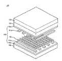
- FIG. 8is a view illustrating a front filter, of a plasma display apparatus according to a first embodiment of the present invention.
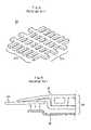
- FIG. 9is a detailed view illustrating a touch screen of FIG. 8 ;
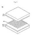
- FIG. 10is a view illustrating a front filter of a plasma display apparatus according to a second embodiment of the present invention.
- FIG. 11is a detailed view illustrating a touch screen shown in FIG. 10 .
- FIG. 8is a view illustrating a front filter of a plasma display apparatus according to a first embodiment of the present invention.
- the front filter 130includes an antireflection coating 150 , an optical characteristic film 152 , a touch screen 156 , and a Near Infrared Ray (Hereinafter, referred to as “NIR”) shield film 158 .
- NIRNear Infrared Ray
- the front filter 130is a film type filter without a glass for support.
- An adhesive layeris formed between respective films 150 , 152 , 156 and 158 of the front filter 130 to adhere respective films 150 , 152 , 156 and 158 to one another.
- a specific substanceis added to the adhesive layer to form the optical characteristic-film 152 .
- a structure of the front filteris a little varied depending on a manufacture enterprise.
- the present inventiondoes not illustrate the adhesive layer for description convenience, and exemplifies the structure of the front filter 130 widely generally used at present.
- the antireflection coating 150prevents an external incident light from being reflected toward an external to improve a contrast of a plasma display panel (PDP).
- the antireflection coating 150is formed on a surface of the front filter 130 . Meanwhile, the antireflection coating 150 can be additionally formed on a rear surface of the front filter 130 .
- the optical characteristic film 152functions to decrease brightness of red (R) and green (G) of visible ray incident from a panel, while it functions to increase brightness of blue (B) to improve an optical characteristic of the PDP.
- the touch screen 156shields EMI (Electromagnetic interference) to prevent the EMI incident from the panel from being emitted to the external.
- the touch screen 156includes an upper film 160 a on which a plurality of first electrode lines 161 a are formed, and a lower film 160 b on which a plurality of second electrode lines 161 b are formed in a direction of crossing with the plurality of first electrode lines 161 a to face the upper film 160 a .
- the plurality of electrode linesis finely structured like a black matrix, it does not influence a picture quality.
- the upper film 160 a and the lower film 160 bare united by a sealant (not shown) coated along an edge portion being a non-touch area, and are spaced away from each other as much as a height of the sealant. Further, a plurality of dot spacers 162 is additionally formed on the plurality of first electrode lines 161 a of the upper film 160 a or the plurality of second electrode lines 161 b of the lower film 160 b at a touch area excepting for the non-touch area to separate the upper film 160 a from the lower film 160 b.
- a transparent film formed of polyethylene terephthalate (PET)is mainly used as the upper film 160 a pressed by a pen or a finger, and a transparent film formed of a material like the upper film 160 a is used as the lower film 160 b .
- At least one of the first and second electrode lines 161 a and 161 bis formed of a dual layer of silver (Ag) and Indium-Tin-Oxide (ITO). Further, at least one of the first and second electrode lines 161 a and 161 b is formed of silver (Ag) or Indium-Tin-oxide (ITO).
- a resistance value of the touch screen 156is varied depending on its contact position. Additionally, since current or voltage is different depending on the varied resistance value, the varied current or voltage is outputted as x-axis and Y-axis coordinate signals through an external electrode not shown connected to the first and second electrode lines 161 a and 161 b.
- the inventive touch screen 156separates the first electrode line 161 a and the second electrode line 161 b from each other to respectively form the first and second electrode lines 161 a and 161 b on the upper/lower films 160 a and 160 b . And then, the plurality of dot spacers 162 is formed between the upper film 160 a and the lower film 160 b . Accordingly, the touch screen 156 shields the EMI to not only prevent the EMI incident from the panel from being emitted to the external but to also perform a function of the touch screen.
- the NIR shield film 158shields the NIR radiated from the panel to prevent the NIR exceeding a reference value from being emitted to the external such that a signal transmitting device using IR (Infrared Ray) can normally transmit a signal such as a remote controller and the like.
- IRInfrared Ray
- FIG. 10is a view illustrating a front filter of a plasma display apparatus according to a second embodiment of the present invention.
- the front filter 230includes an antireflection coating 250 , an optical characteristic film 252 , a touch screen 256 , and a Near Infrared Ray (Hereinafter, referred to as “NIR”) shield film 258 .
- NIRNear Infrared Ray
- the front filter 230is a film type filter without a glass for support.
- An adhesive layeris formed between respective films 250 , 252 , 256 and 258 of the front filter 230 to adhere respective films 250 , 252 , 256 and 258 to one another.
- a specific substanceis added to the adhesive layer to form the optical characteristic film 252 .
- the antireflection coating 250prevents an external incident light from being reflected toward an external to improve a contrast of a plasma display panel (PDP).
- the antireflection coating 250is formed on a surface of the front filter 230 . Meanwhile, the antireflection coating 250 can be additionally formed on the rear surface of the front filter 230 .
- the optical characteristic film 252functions to decrease brightness of red (R) and green (G) of visible ray incident from a panel, while it functions to increase brightness of blue (B) to improve an optical characteristic of the PDP.
- the touch screen 256shields 8 MI (Electromagnetic interference) to prevent the EMI incident from the panel from being emitted to the external.
- the touch screen 256includes an upper film 260 a on which a plurality of first transparent conductive layers 261 a are formed, and a lower film 260 b on which a plurality of second transparent conductive layers 261 b are formed in a direction of crossing with the plurality of first transparent conductive layers 261 a to face the upper film 260 a.
- the upper film 260 a and the lower film 260 bare united by a sealant (not shown) coated along an edge portion being a non-touch area and are spaced away from each other as much as a height of the sealant. Further, a plurality of dot spacers 262 is additionally formed on the plurality of first transparent conductive layers 261 a of the upper film 260 a or the plurality of second transparent conductive layers 261 b of the lower film 260 b at a touch area excepting for the non-touch area to separate the upper film 260 a from the lower film 260 b.
- a transparent film formed of polyethylene terephthalate (PET)is mainly used as the upper film 260 a pressed by a pen or a finger, and a transparent film formed of a material like the upper film 260 a is used as the lower film 260 b .
- first and second transparent conductive layers 261 a and 261 bindium-tin-oxide (ITO) is used.
- a resistance value of the touch screen 256is varied depending on its contact position. Additionally, since current or voltage is different depending on the varied resistance value, the varied current or voltage is outputted as X-axis and Y-axis coordinate signals through an external electrode not shown connected to the first and second transparent conductive layers 261 a and 261 b.
- the inventive touch screen 256separates the first transparent conductive layer 261 a and the second transparent conductive layer 261 b from each other to respectively form the first and second transparent conductive layers 261 a and 261 b on the upper/lower films 260 a and 260 b . And then, the plurality of dot spacers 262 is formed between the upper film 260 a and the lower film 260 b . Accordingly, the touch screen 256 shields the EMI to not only prevent the EMI incident from the panel from being emitted to the external, but to also perform a function of the touch screen.
- the NIR shield film 258shields the NIR radiated from the panel to prevent the NIP exceeding a reference value from being emitted to the external such that a signal transmitting device using IR (Infrared Ray) can normally transmit a signal such as a remote controller and the like.
- IRInfrared Ray
- the above-described film typed front filterhas an advantage of light weight and also slim in comparison to a glass typed front filter. Further, the film typed front filter can reduce a manufacture cost in comparison to the glass typed front filter.
- the present inventiondoes not require an external separate input unit. Further, the present invention not only appeals to consumer's mentality, but also enhances a value of a high-class brand.
- the present inventioncan also use the touch screen to add an automatic positioning and screen adjustment function, and an additional function such as color depth adjustment, resolution adjustment and brightness adjustment.
- the present inventioncan provide the touch screen for the front filter installed in the plasma display apparatus to not only add various functions, but to also appeal to the consumer's mentality and enhance the value of the high-class brand.
Landscapes
- Engineering & Computer Science (AREA)
- Physics & Mathematics (AREA)
- Plasma & Fusion (AREA)
- General Engineering & Computer Science (AREA)
- Theoretical Computer Science (AREA)
- Electromagnetism (AREA)
- Human Computer Interaction (AREA)
- General Physics & Mathematics (AREA)
- Devices For Indicating Variable Information By Combining Individual Elements (AREA)
- Position Input By Displaying (AREA)
Abstract
Description
Claims (22)
Applications Claiming Priority (2)
| Application Number | Priority Date | Filing Date | Title |
|---|---|---|---|
| KR2003/15174 | 2003-03-11 | ||
| KR10-2003-0015174AKR100509763B1 (en) | 2003-03-11 | 2003-03-11 | Front filter of plasma display panel |
Publications (2)
| Publication Number | Publication Date |
|---|---|
| US20040178729A1 US20040178729A1 (en) | 2004-09-16 |
| US7242136B2true US7242136B2 (en) | 2007-07-10 |
Family
ID=32768632
Family Applications (1)
| Application Number | Title | Priority Date | Filing Date |
|---|---|---|---|
| US10/796,102Expired - Fee RelatedUS7242136B2 (en) | 2003-03-11 | 2004-03-10 | Front filter, and plasma display apparatus having the same |
Country Status (6)
| Country | Link |
|---|---|
| US (1) | US7242136B2 (en) |
| EP (1) | EP1458004B1 (en) |
| JP (1) | JP2004272920A (en) |
| KR (1) | KR100509763B1 (en) |
| CN (1) | CN1530668A (en) |
| DE (1) | DE602004021208D1 (en) |
Cited By (42)
| Publication number | Priority date | Publication date | Assignee | Title |
|---|---|---|---|---|
| US20060279211A1 (en)* | 2005-06-10 | 2006-12-14 | Lg Electronics Inc. | Plasma display panel |
| US20090102810A1 (en)* | 2007-10-23 | 2009-04-23 | Tsinghua University | Touch panel |
| US20090101488A1 (en)* | 2007-10-23 | 2009-04-23 | Tsinghua University | Touch panel |
| US20090153504A1 (en)* | 2007-12-14 | 2009-06-18 | Tsinghua University | Touch panel, method for making the same, and display device adopting the same |
| US20090153513A1 (en)* | 2007-12-14 | 2009-06-18 | Tsinghua University | Touch panel, method for making the same, and display device adopting the same |
| US20090153514A1 (en)* | 2007-12-12 | 2009-06-18 | Tsinghua University | Touch panel and display device using the same |
| US20090153507A1 (en)* | 2007-12-12 | 2009-06-18 | Tsinghua University | Touch panel and display device using the same |
| US20090153505A1 (en)* | 2007-12-12 | 2009-06-18 | Tsinghua University | Touch panel and display device using the same |
| US20090153515A1 (en)* | 2007-12-12 | 2009-06-18 | Tsinghua University | Touch panel and display device using the same |
| US20090153509A1 (en)* | 2007-12-14 | 2009-06-18 | Tsinghua University | Touch panel and display device using the same |
| US20090153520A1 (en)* | 2007-12-12 | 2009-06-18 | Tsinghua University | Touch panel and display device using the same |
| US20090153521A1 (en)* | 2007-12-14 | 2009-06-18 | Tsinghua University | Touch panel and display device using the same |
| US20090153503A1 (en)* | 2007-12-12 | 2009-06-18 | Tsinghua University | Touch panel and display device using the same |
| US20090153516A1 (en)* | 2007-12-12 | 2009-06-18 | Tsinghua University | Touch panel, method for making the same, and display device adopting the same |
| US20090153508A1 (en)* | 2007-12-14 | 2009-06-18 | Tsinghua University | Touch panel and display device using the same |
| US20090153512A1 (en)* | 2007-12-12 | 2009-06-18 | Tsinghua University | Touch panel and display device using the same |
| US20090153510A1 (en)* | 2007-12-14 | 2009-06-18 | Tsinghua University | Touch panel and display device using the same |
| US20090153502A1 (en)* | 2007-12-14 | 2009-06-18 | Tsinghua University | Touch panel and display device using the same |
| US20090153506A1 (en)* | 2007-12-14 | 2009-06-18 | Tsinghua University | Touch panel, method for making the same, and display device adopting the same |
| US20090153511A1 (en)* | 2007-12-12 | 2009-06-18 | Tsinghua University | Touch panel and display device using the same |
| US20090159188A1 (en)* | 2007-12-21 | 2009-06-25 | Tsinghua University | Method for making touch panel |
| US20090160799A1 (en)* | 2007-12-21 | 2009-06-25 | Tsinghua University | Method for making touch panel |
| US20090160796A1 (en)* | 2007-12-21 | 2009-06-25 | Tsinghua University | Touch panel and display device using the same |
| US20090160795A1 (en)* | 2007-12-21 | 2009-06-25 | Tsinghua University | Touch panel and display device using the same |
| US20090160798A1 (en)* | 2007-12-21 | 2009-06-25 | Tsinghua University | Touch panel and display device using the same |
| US20090160797A1 (en)* | 2007-12-21 | 2009-06-25 | Tsinghua University | Touch panel and display device using the same |
| US20090167711A1 (en)* | 2007-12-27 | 2009-07-02 | Tsinghua University | Touch panel and display device using the same |
| US20090167709A1 (en)* | 2007-12-27 | 2009-07-02 | Tsinghua University | Touch panel and display device using the same |
| US20090167707A1 (en)* | 2007-12-27 | 2009-07-02 | Tsinghua University | Touch control device |
| US20090167710A1 (en)* | 2007-12-27 | 2009-07-02 | Tsinghua University | Touch panel and display device using the same |
| US20090167708A1 (en)* | 2007-12-27 | 2009-07-02 | Tsinghua University | Touch panel and display device using the same |
| US20090273581A1 (en)* | 2008-04-30 | 2009-11-05 | Samsung Corning Precision Glass Co., Ltd. | Display filter and display device having the same |
| US20100001971A1 (en)* | 2008-07-04 | 2010-01-07 | Tsinghua University | Liquid crystal display screen |
| US20100001975A1 (en)* | 2008-07-04 | 2010-01-07 | Tsinghua University | Portable computer |
| US20100048254A1 (en)* | 2008-08-22 | 2010-02-25 | Tsinghua University | Mobile phone |
| US20100048250A1 (en)* | 2008-08-22 | 2010-02-25 | Tsinghua University | Personal digital assistant |
| US20100073322A1 (en)* | 2008-09-19 | 2010-03-25 | Tsinghua University | Desktop computer |
| US20100317409A1 (en)* | 2009-06-12 | 2010-12-16 | Tsinghua University | Carbon nanotube based flexible mobile phone |
| US20110102347A1 (en)* | 2009-10-30 | 2011-05-05 | Samsung Corining Precision Materials Co., Ltd. | Display filter having touch input function |
| US20110171419A1 (en)* | 2007-12-12 | 2011-07-14 | Tsinghua University | Electronic element having carbon nanotubes |
| US8390580B2 (en) | 2008-07-09 | 2013-03-05 | Tsinghua University | Touch panel, liquid crystal display screen using the same, and methods for making the touch panel and the liquid crystal display screen |
| USRE45559E1 (en) | 1997-10-28 | 2015-06-09 | Apple Inc. | Portable computers |
Families Citing this family (12)
| Publication number | Priority date | Publication date | Assignee | Title |
|---|---|---|---|---|
| KR100669785B1 (en)* | 2004-11-25 | 2007-01-16 | 삼성에스디아이 주식회사 | Plasma display module |
| US7524920B2 (en)* | 2004-12-16 | 2009-04-28 | Eastman Chemical Company | Biaxially oriented copolyester film and laminates thereof |
| US20060244678A1 (en)* | 2005-04-29 | 2006-11-02 | Lg Electronics Inc | Filter for display apparatus and plasma display apparatus comprising filter |
| US20060275558A1 (en)* | 2005-05-17 | 2006-12-07 | Pecorini Thomas J | Conductively coated substrates derived from biaxially-oriented and heat-set polyester film |
| KR100769907B1 (en)* | 2006-07-12 | 2007-10-24 | 엘지전자 주식회사 | Plasma display device |
| KR101387531B1 (en)* | 2008-01-21 | 2014-04-21 | 엘지전자 주식회사 | Plasma display panel having a touch-screen and Method for fabricating in threrof |
| US8508488B2 (en)* | 2008-06-12 | 2013-08-13 | Samsung Sdi Co., Ltd. | Display apparatus having touch screen function |
| KR20100053349A (en)* | 2008-11-12 | 2010-05-20 | 엘지전자 주식회사 | Touch module, fabaricating method thereof, and portable terminal having the same |
| TWI383312B (en)* | 2008-11-13 | 2013-01-21 | Orise Technology Co Ltd | Method for detecting touch point and touch panel using the same |
| KR101016676B1 (en) | 2008-12-01 | 2011-02-25 | 삼성에스디아이 주식회사 | Plasma display device and driving method thereof |
| CN102496546A (en)* | 2011-12-28 | 2012-06-13 | 四川虹欧显示器件有限公司 | Plasma display screen and manufacturing method thereof |
| CN105631239B (en)* | 2014-10-30 | 2018-08-17 | 国际商业机器公司 | Method and apparatus for managing gene order |
Citations (11)
| Publication number | Priority date | Publication date | Assignee | Title |
|---|---|---|---|---|
| US4794634A (en)* | 1985-12-24 | 1988-12-27 | Kabushiki Kaisha Komatsu Seisakusho | Position-sensitive photodetector and light transmissive tablet and light-emitting pen |
| JPH10163671A (en)* | 1996-11-28 | 1998-06-19 | Mitsubishi Electric Corp | Plasma display device |
| US6061177A (en)* | 1996-12-19 | 2000-05-09 | Fujimoto; Kenneth Noboru | Integrated computer display and graphical input apparatus and method |
| US6087012A (en)* | 1994-07-29 | 2000-07-11 | Donnelly Corporation | Transparent substrate with diffuser surface |
| US6215477B1 (en)* | 1997-10-22 | 2001-04-10 | Smart Technologies Inc. | Touch sensitive display panel |
| US20030122801A1 (en)* | 2001-12-27 | 2003-07-03 | Lg.Philips Lcd Co., Ltd. | Liquid crystal panel device having a touch panel and method of fabricating the same |
| US20050062410A1 (en)* | 2001-10-11 | 2005-03-24 | Bell Gareth Paul | Visual display unit illumination |
| US6876355B1 (en)* | 2000-05-18 | 2005-04-05 | Lg. Philips Lcd Co., Ltd. | Touch screen structure to prevent image distortion |
| US6887631B2 (en)* | 2001-06-01 | 2005-05-03 | Seiko Epson Corporation | Color filter and electro-optical device |
| US6933086B2 (en)* | 2001-06-01 | 2005-08-23 | Seiko Epson Corporation | Color filter, display device and electronic equipment, manufacturing method thereof, and apparatus for manufacturing display device |
| US7053886B2 (en)* | 2001-12-27 | 2006-05-30 | Lg.Philips Lcd Co., Ltd. | Liquid crystal panel device having a touch panel and method for driving the same |
Family Cites Families (12)
| Publication number | Priority date | Publication date | Assignee | Title |
|---|---|---|---|---|
| JPS63174212A (en)* | 1987-01-09 | 1988-07-18 | グンゼ株式会社 | Transparent electrode sheet and transparent touch panel |
| JPH07282674A (en)* | 1994-04-12 | 1995-10-27 | Nissha Printing Co Ltd | Manufacture of transparent touch panel |
| JPH08287775A (en)* | 1995-04-17 | 1996-11-01 | Brother Ind Ltd | Touch panel |
| JPH09145918A (en)* | 1995-11-22 | 1997-06-06 | Fujitsu General Ltd | Filter device |
| JP2000105541A (en)* | 1998-07-28 | 2000-04-11 | Sumitomo Chem Co Ltd | Display front panel |
| TW412644B (en)* | 1998-07-28 | 2000-11-21 | Sumitomo Chemical Co | Front panel for display |
| JP2000181626A (en)* | 1998-12-16 | 2000-06-30 | Pioneer Electronic Corp | Display device |
| AU4712400A (en)* | 1999-05-14 | 2000-12-05 | 3M Innovative Properties Company | Ablation enhancement layer |
| JP2000351170A (en)* | 1999-06-10 | 2000-12-19 | Gunze Ltd | Transparent conductive laminate |
| US6555235B1 (en)* | 2000-07-06 | 2003-04-29 | 3M Innovative Properties Co. | Touch screen system |
| US6587097B1 (en)* | 2000-11-28 | 2003-07-01 | 3M Innovative Properties Co. | Display system |
| JP4660977B2 (en)* | 2001-06-15 | 2011-03-30 | パナソニック株式会社 | Plasma display device |
- 2003
- 2003-03-11KRKR10-2003-0015174Apatent/KR100509763B1/ennot_activeExpired - Fee Related
- 2004
- 2004-03-10USUS10/796,102patent/US7242136B2/ennot_activeExpired - Fee Related
- 2004-03-11CNCNA2004100085010Apatent/CN1530668A/enactivePending
- 2004-03-11DEDE602004021208Tpatent/DE602004021208D1/ennot_activeExpired - Lifetime
- 2004-03-11JPJP2004068841Apatent/JP2004272920A/enactivePending
- 2004-03-11EPEP04075717Apatent/EP1458004B1/ennot_activeExpired - Lifetime
Patent Citations (11)
| Publication number | Priority date | Publication date | Assignee | Title |
|---|---|---|---|---|
| US4794634A (en)* | 1985-12-24 | 1988-12-27 | Kabushiki Kaisha Komatsu Seisakusho | Position-sensitive photodetector and light transmissive tablet and light-emitting pen |
| US6087012A (en)* | 1994-07-29 | 2000-07-11 | Donnelly Corporation | Transparent substrate with diffuser surface |
| JPH10163671A (en)* | 1996-11-28 | 1998-06-19 | Mitsubishi Electric Corp | Plasma display device |
| US6061177A (en)* | 1996-12-19 | 2000-05-09 | Fujimoto; Kenneth Noboru | Integrated computer display and graphical input apparatus and method |
| US6215477B1 (en)* | 1997-10-22 | 2001-04-10 | Smart Technologies Inc. | Touch sensitive display panel |
| US6876355B1 (en)* | 2000-05-18 | 2005-04-05 | Lg. Philips Lcd Co., Ltd. | Touch screen structure to prevent image distortion |
| US6887631B2 (en)* | 2001-06-01 | 2005-05-03 | Seiko Epson Corporation | Color filter and electro-optical device |
| US6933086B2 (en)* | 2001-06-01 | 2005-08-23 | Seiko Epson Corporation | Color filter, display device and electronic equipment, manufacturing method thereof, and apparatus for manufacturing display device |
| US20050062410A1 (en)* | 2001-10-11 | 2005-03-24 | Bell Gareth Paul | Visual display unit illumination |
| US20030122801A1 (en)* | 2001-12-27 | 2003-07-03 | Lg.Philips Lcd Co., Ltd. | Liquid crystal panel device having a touch panel and method of fabricating the same |
| US7053886B2 (en)* | 2001-12-27 | 2006-05-30 | Lg.Philips Lcd Co., Ltd. | Liquid crystal panel device having a touch panel and method for driving the same |
Cited By (91)
| Publication number | Priority date | Publication date | Assignee | Title |
|---|---|---|---|---|
| USRE45559E1 (en) | 1997-10-28 | 2015-06-09 | Apple Inc. | Portable computers |
| USRE46548E1 (en) | 1997-10-28 | 2017-09-12 | Apple Inc. | Portable computers |
| US7605538B2 (en)* | 2005-06-10 | 2009-10-20 | Lg Electronics Inc. | Plasma display panel |
| US20060279211A1 (en)* | 2005-06-10 | 2006-12-14 | Lg Electronics Inc. | Plasma display panel |
| US8248377B2 (en) | 2007-10-23 | 2012-08-21 | Tsinghua University | Touch panel |
| US20090102810A1 (en)* | 2007-10-23 | 2009-04-23 | Tsinghua University | Touch panel |
| US20090101488A1 (en)* | 2007-10-23 | 2009-04-23 | Tsinghua University | Touch panel |
| US8502786B2 (en) | 2007-10-23 | 2013-08-06 | Tsinghua University | Touch panel |
| US20090153505A1 (en)* | 2007-12-12 | 2009-06-18 | Tsinghua University | Touch panel and display device using the same |
| US8248381B2 (en) | 2007-12-12 | 2012-08-21 | Tsinghua University | Touch panel and display device using the same |
| US20090153520A1 (en)* | 2007-12-12 | 2009-06-18 | Tsinghua University | Touch panel and display device using the same |
| US20110171419A1 (en)* | 2007-12-12 | 2011-07-14 | Tsinghua University | Electronic element having carbon nanotubes |
| US20090153503A1 (en)* | 2007-12-12 | 2009-06-18 | Tsinghua University | Touch panel and display device using the same |
| US20090153516A1 (en)* | 2007-12-12 | 2009-06-18 | Tsinghua University | Touch panel, method for making the same, and display device adopting the same |
| US8237674B2 (en) | 2007-12-12 | 2012-08-07 | Tsinghua University | Touch panel and display device using the same |
| US20090153512A1 (en)* | 2007-12-12 | 2009-06-18 | Tsinghua University | Touch panel and display device using the same |
| US8237671B2 (en) | 2007-12-12 | 2012-08-07 | Tsinghua University | Touch panel and display device using the same |
| US8237670B2 (en) | 2007-12-12 | 2012-08-07 | Tsinghua University | Touch panel and display device using the same |
| US20090153515A1 (en)* | 2007-12-12 | 2009-06-18 | Tsinghua University | Touch panel and display device using the same |
| US20090153511A1 (en)* | 2007-12-12 | 2009-06-18 | Tsinghua University | Touch panel and display device using the same |
| US8325585B2 (en) | 2007-12-12 | 2012-12-04 | Tsinghua University | Touch panel and display device using the same |
| US20090153507A1 (en)* | 2007-12-12 | 2009-06-18 | Tsinghua University | Touch panel and display device using the same |
| US20090153514A1 (en)* | 2007-12-12 | 2009-06-18 | Tsinghua University | Touch panel and display device using the same |
| US9040159B2 (en) | 2007-12-12 | 2015-05-26 | Tsinghua University | Electronic element having carbon nanotubes |
| US8542212B2 (en) | 2007-12-12 | 2013-09-24 | Tsinghua University | Touch panel, method for making the same, and display device adopting the same |
| US8199119B2 (en) | 2007-12-12 | 2012-06-12 | Beijing Funate Innovation Technology Co., Ltd. | Touch panel and display device using the same |
| US8115742B2 (en) | 2007-12-12 | 2012-02-14 | Tsinghua University | Touch panel and display device using the same |
| US8363017B2 (en) | 2007-12-12 | 2013-01-29 | Beijing Funate Innovation Technology Co., Ltd. | Touch panel and display device using the same |
| US20090153521A1 (en)* | 2007-12-14 | 2009-06-18 | Tsinghua University | Touch panel and display device using the same |
| US8253700B2 (en) | 2007-12-14 | 2012-08-28 | Tsinghua University | Touch panel and display device using the same |
| US8253701B2 (en) | 2007-12-14 | 2012-08-28 | Tsinghua University | Touch panel, method for making the same, and display device adopting the same |
| US8411044B2 (en) | 2007-12-14 | 2013-04-02 | Tsinghua University | Touch panel, method for making the same, and display device adopting the same |
| US8248380B2 (en) | 2007-12-14 | 2012-08-21 | Tsinghua University | Touch panel and display device using the same |
| US8248379B2 (en) | 2007-12-14 | 2012-08-21 | Tsinghua University | Touch panel, method for making the same, and display device adopting the same |
| US20090153506A1 (en)* | 2007-12-14 | 2009-06-18 | Tsinghua University | Touch panel, method for making the same, and display device adopting the same |
| US20090153502A1 (en)* | 2007-12-14 | 2009-06-18 | Tsinghua University | Touch panel and display device using the same |
| US8243029B2 (en) | 2007-12-14 | 2012-08-14 | Tsinghua University | Touch panel and display device using the same |
| US20090153510A1 (en)* | 2007-12-14 | 2009-06-18 | Tsinghua University | Touch panel and display device using the same |
| US8237673B2 (en) | 2007-12-14 | 2012-08-07 | Tsinghua University | Touch panel and display device using the same |
| US20090153508A1 (en)* | 2007-12-14 | 2009-06-18 | Tsinghua University | Touch panel and display device using the same |
| US20090153509A1 (en)* | 2007-12-14 | 2009-06-18 | Tsinghua University | Touch panel and display device using the same |
| US8237672B2 (en) | 2007-12-14 | 2012-08-07 | Tsinghua University | Touch panel and display device using the same |
| US20090153513A1 (en)* | 2007-12-14 | 2009-06-18 | Tsinghua University | Touch panel, method for making the same, and display device adopting the same |
| US20090153504A1 (en)* | 2007-12-14 | 2009-06-18 | Tsinghua University | Touch panel, method for making the same, and display device adopting the same |
| US20090160796A1 (en)* | 2007-12-21 | 2009-06-25 | Tsinghua University | Touch panel and display device using the same |
| US20090160797A1 (en)* | 2007-12-21 | 2009-06-25 | Tsinghua University | Touch panel and display device using the same |
| US20090159188A1 (en)* | 2007-12-21 | 2009-06-25 | Tsinghua University | Method for making touch panel |
| US8111245B2 (en) | 2007-12-21 | 2012-02-07 | Tsinghua University | Touch panel and display device using the same |
| US20090160799A1 (en)* | 2007-12-21 | 2009-06-25 | Tsinghua University | Method for making touch panel |
| US8243030B2 (en) | 2007-12-21 | 2012-08-14 | Tsinghua University | Touch panel and display device using the same |
| US20090160795A1 (en)* | 2007-12-21 | 2009-06-25 | Tsinghua University | Touch panel and display device using the same |
| US8585855B2 (en) | 2007-12-21 | 2013-11-19 | Tsinghua University | Method for making touch panel |
| US8574393B2 (en) | 2007-12-21 | 2013-11-05 | Tsinghua University | Method for making touch panel |
| US20090160798A1 (en)* | 2007-12-21 | 2009-06-25 | Tsinghua University | Touch panel and display device using the same |
| US8325146B2 (en) | 2007-12-21 | 2012-12-04 | Tsinghua University | Touch panel and display device using the same |
| US8248378B2 (en) | 2007-12-21 | 2012-08-21 | Tsinghua University | Touch panel and display device using the same |
| US20090167711A1 (en)* | 2007-12-27 | 2009-07-02 | Tsinghua University | Touch panel and display device using the same |
| US8237669B2 (en) | 2007-12-27 | 2012-08-07 | Tsinghua University | Touch panel and display device using the same |
| US20090167709A1 (en)* | 2007-12-27 | 2009-07-02 | Tsinghua University | Touch panel and display device using the same |
| US8237668B2 (en) | 2007-12-27 | 2012-08-07 | Tsinghua University | Touch control device |
| US8325145B2 (en) | 2007-12-27 | 2012-12-04 | Tsinghua University | Touch panel and display device using the same |
| US20090167707A1 (en)* | 2007-12-27 | 2009-07-02 | Tsinghua University | Touch control device |
| US20090167710A1 (en)* | 2007-12-27 | 2009-07-02 | Tsinghua University | Touch panel and display device using the same |
| US8237675B2 (en) | 2007-12-27 | 2012-08-07 | Tsinghua University | Touch panel and display device using the same |
| US20090167708A1 (en)* | 2007-12-27 | 2009-07-02 | Tsinghua University | Touch panel and display device using the same |
| US8125878B2 (en) | 2007-12-27 | 2012-02-28 | Tsinghua University | Touch panel and display device using the same |
| US20090273581A1 (en)* | 2008-04-30 | 2009-11-05 | Samsung Corning Precision Glass Co., Ltd. | Display filter and display device having the same |
| US8237679B2 (en) | 2008-07-04 | 2012-08-07 | Tsinghua University | Liquid crystal display screen |
| US8199123B2 (en) | 2008-07-04 | 2012-06-12 | Tsinghua University | Method for making liquid crystal display screen |
| US20100001972A1 (en)* | 2008-07-04 | 2010-01-07 | Tsinghua University | Touch Panel |
| US20100001975A1 (en)* | 2008-07-04 | 2010-01-07 | Tsinghua University | Portable computer |
| US20100001976A1 (en)* | 2008-07-04 | 2010-01-07 | Tsinghua University | Liquid crystal display screen |
| US20100041297A1 (en)* | 2008-07-04 | 2010-02-18 | Tsinghua University | Method for making liquid crystal display adopting touch panel |
| US8105126B2 (en) | 2008-07-04 | 2012-01-31 | Tsinghua University | Method for fabricating touch panel |
| US20100093247A1 (en)* | 2008-07-04 | 2010-04-15 | Tsinghua University | Method for fabricating touch panel |
| US8237677B2 (en) | 2008-07-04 | 2012-08-07 | Tsinghua University | Liquid crystal display screen |
| US8237680B2 (en) | 2008-07-04 | 2012-08-07 | Tsinghua University | Touch panel |
| US20100093117A1 (en)* | 2008-07-04 | 2010-04-15 | Tsinghua University | Method for making liquid crystal display screen |
| US20100001971A1 (en)* | 2008-07-04 | 2010-01-07 | Tsinghua University | Liquid crystal display screen |
| US8228308B2 (en) | 2008-07-04 | 2012-07-24 | Tsinghua University | Method for making liquid crystal display adopting touch panel |
| US8390580B2 (en) | 2008-07-09 | 2013-03-05 | Tsinghua University | Touch panel, liquid crystal display screen using the same, and methods for making the touch panel and the liquid crystal display screen |
| US8411052B2 (en) | 2008-07-09 | 2013-04-02 | Tsinghua University | Touch panel, liquid crystal display screen using the same, and methods for making the touch panel and the liquid crystal display screen |
| US8411051B2 (en) | 2008-07-09 | 2013-04-02 | Tsinghua University | Liquid crystal display screen |
| US20100048250A1 (en)* | 2008-08-22 | 2010-02-25 | Tsinghua University | Personal digital assistant |
| US8346316B2 (en) | 2008-08-22 | 2013-01-01 | Tsinghua University | Personal digital assistant |
| US20100048254A1 (en)* | 2008-08-22 | 2010-02-25 | Tsinghua University | Mobile phone |
| US8260378B2 (en) | 2008-08-22 | 2012-09-04 | Tsinghua University | Mobile phone |
| US20100073322A1 (en)* | 2008-09-19 | 2010-03-25 | Tsinghua University | Desktop computer |
| US20100317409A1 (en)* | 2009-06-12 | 2010-12-16 | Tsinghua University | Carbon nanotube based flexible mobile phone |
| US9077793B2 (en) | 2009-06-12 | 2015-07-07 | Tsinghua University | Carbon nanotube based flexible mobile phone |
| US20110102347A1 (en)* | 2009-10-30 | 2011-05-05 | Samsung Corining Precision Materials Co., Ltd. | Display filter having touch input function |
Also Published As
| Publication number | Publication date |
|---|---|
| EP1458004B1 (en) | 2009-05-27 |
| KR100509763B1 (en) | 2005-08-25 |
| CN1530668A (en) | 2004-09-22 |
| EP1458004A1 (en) | 2004-09-15 |
| JP2004272920A (en) | 2004-09-30 |
| US20040178729A1 (en) | 2004-09-16 |
| KR20040080270A (en) | 2004-09-18 |
| DE602004021208D1 (en) | 2009-07-09 |
Similar Documents
| Publication | Publication Date | Title |
|---|---|---|
| US7242136B2 (en) | Front filter, and plasma display apparatus having the same | |
| US7321186B2 (en) | Front filter, and plasma display apparatus having the same | |
| US20070001929A1 (en) | Plasma display panel having a grounding structure of a film type front surface filter | |
| US7193779B2 (en) | Front filter in plasma display panel | |
| USRE42233E1 (en) | Plasma display apparatus | |
| US20070188854A1 (en) | Front filter in plasma display panel | |
| US20050017620A1 (en) | Display panel module | |
| KR20040085765A (en) | Front-filter of film type using plasma display panel | |
| US20060097650A1 (en) | Plasma display apparatus comprising filter | |
| KR100911034B1 (en) | Front filter of plasma display panel | |
| KR100516935B1 (en) | Plasma display panel | |
| US20110031883A1 (en) | Plasma display apparatus to reduce emi emission | |
| KR100516939B1 (en) | Plasma display panel | |
| KR100709879B1 (en) | Film filter of plasma display panel | |
| US7605538B2 (en) | Plasma display panel | |
| KR20040088700A (en) | Front-filter and display panel module using the same | |
| CN100565624C (en) | Plasmia indicating panel | |
| KR20050023559A (en) | Display Panel Moudle | |
| US8369106B2 (en) | Plasma display apparatus to reduce EMI emission | |
| KR20040064761A (en) | Base film of front filter | |
| KR20040085766A (en) | Electromagnetic wave shielding film of plasma display panel | |
| US20110032234A1 (en) | Plasma display apparatus to reduce emi emission | |
| KR20070091849A (en) | Plasma display device | |
| KR20070116467A (en) | Plasma Display Panel And Method Of Making The Same |
Legal Events
| Date | Code | Title | Description |
|---|---|---|---|
| AS | Assignment | Owner name:LG ELECTRONICS INC., KOREA, REPUBLIC OF Free format text:ASSIGNMENT OF ASSIGNORS INTEREST;ASSIGNORS:KIM, YOUNG SUNG;KIM, KYUNG KU;CHA, HONG RAE;AND OTHERS;REEL/FRAME:015068/0418 Effective date:20040303 | |
| STCF | Information on status: patent grant | Free format text:PATENTED CASE | |
| FEPP | Fee payment procedure | Free format text:PAYOR NUMBER ASSIGNED (ORIGINAL EVENT CODE: ASPN); ENTITY STATUS OF PATENT OWNER: LARGE ENTITY | |
| CC | Certificate of correction | ||
| FEPP | Fee payment procedure | Free format text:PAYOR NUMBER ASSIGNED (ORIGINAL EVENT CODE: ASPN); ENTITY STATUS OF PATENT OWNER: LARGE ENTITY Free format text:PAYER NUMBER DE-ASSIGNED (ORIGINAL EVENT CODE: RMPN); ENTITY STATUS OF PATENT OWNER: LARGE ENTITY | |
| FPAY | Fee payment | Year of fee payment:4 | |
| FPAY | Fee payment | Year of fee payment:8 | |
| FEPP | Fee payment procedure | Free format text:MAINTENANCE FEE REMINDER MAILED (ORIGINAL EVENT CODE: REM.); ENTITY STATUS OF PATENT OWNER: LARGE ENTITY | |
| LAPS | Lapse for failure to pay maintenance fees | Free format text:PATENT EXPIRED FOR FAILURE TO PAY MAINTENANCE FEES (ORIGINAL EVENT CODE: EXP.); ENTITY STATUS OF PATENT OWNER: LARGE ENTITY | |
| STCH | Information on status: patent discontinuation | Free format text:PATENT EXPIRED DUE TO NONPAYMENT OF MAINTENANCE FEES UNDER 37 CFR 1.362 | |
| FP | Lapsed due to failure to pay maintenance fee | Effective date:20190710 |