US7241632B2 - MTJ read head with sidewall spacers - Google Patents
MTJ read head with sidewall spacersDownload PDFInfo
- Publication number
- US7241632B2 US7241632B2US11/106,320US10632005AUS7241632B2US 7241632 B2US7241632 B2US 7241632B2US 10632005 AUS10632005 AUS 10632005AUS 7241632 B2US7241632 B2US 7241632B2
- Authority
- US
- United States
- Prior art keywords
- layer
- silicon nitride
- cmp
- mtj
- silicon oxide
- Prior art date
- Legal status (The legal status is an assumption and is not a legal conclusion. Google has not performed a legal analysis and makes no representation as to the accuracy of the status listed.)
- Expired - Lifetime, expires
Links
Images


Classifications
- H—ELECTRICITY
- H10—SEMICONDUCTOR DEVICES; ELECTRIC SOLID-STATE DEVICES NOT OTHERWISE PROVIDED FOR
- H10N—ELECTRIC SOLID-STATE DEVICES NOT OTHERWISE PROVIDED FOR
- H10N50/00—Galvanomagnetic devices
- H10N50/01—Manufacture or treatment
Definitions
- the inventionrelates to the general field of magnetic disk storage with particular reference to reducing the occurrence of shorts in MTJs (magnetic tunnel junctions).
- MRAM (magnetic random access memory) architecturecan be based on MTJs that sit at the intersection points of orthogonal wires running above and below them.
- a typical MTJ film stackis shown in FIG. 1 . Seen at the top of the MTJ cell stack is cap layer 11 , of (for example) tantalum.
- the reading of stored datacan be accomplished by passing a low current through the MTJ.
- the orientation of its magnetic moment, parallel or antiparallel,determines in which of two possible resistance states tunnel barrier 13 happens to be, thereby defining a pair of binary memory states.
- seed layer 16Also seen in FIG. 1 are seed layer 16 , pinning layer 15 , pinned layer (or layers if a trilayer synthetic antiferromagnetic is used) 14 , dielectric tunneling layer 13 , and free layer 12 .
- the latteris itself often made up of two or more layers.
- CMPchemical mechanical polishing
- CMPpolishing rate
- CMPshould terminate right at the MTJ cap layer but, due to CMP non-uniformity and pattern dependence, the process requires over-polishing in order to ensure the complete exposure of the MTJ cap layer. If the cap layer removal rate is slower than the dielectric removal rate, MTJ caps will protrude through the dielectric layer at the conclusion of CMP. A protruded MTJ cap is vulnerable to the occurrence of electrical shorts.
- U.S. Pat. No. 6,475,857(Kim et al) describes dielectric sidewall spacers, but they are removed.
- U.S. Patent Application 2004/0205958(Grynkewich et al) discloses sidewall spacers and a masking tab to reduce the likelihood of electrical shorting by preventing deposition of metallic particles during etching of the metal layers of the MTJ. The spacers also prevent shorting if a via overlying the MTJ stack is misaligned.
- U.S. Patent Application 2004/0191928(Shi) shows sidewall spacers on an MTJ stack.
- Another object of at least one embodiment of the present inventionhas been to provide one or more processes for the manufacture of said stack.
- FIG. 1is a schematic cross-section of a typical MTJ stack.
- FIG. 2shows the starting point for both process embodiments.
- FIG. 3illustrates formation of tapered silicon nitride spacers.
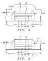
- FIGS. 4-5show that while the cap layer has protruded above the surrounding layer of silicon oxide, its sidewalls are protected by the spacers illustrated in FIG. 3 .
- FIGS. 6-8illustrate the formation of silicon nitride spacers of uniform thickness.
- FIGS. 9-10show that while the cap layer has protruded above the surrounding layer of silicon oxide, its sidewalls are protected by spacers of uniform thickness.
- silicon nitride layer 22is deposited using a conformal deposition method such as low-pressure chemical vapor deposition (LPCVD) from, for example, a BTBAS (bis(tertiary-butylamino) silane) source.
- LPCVDlow-pressure chemical vapor deposition
- Typical deposition conditionsare a BTBAS flow in the range of 40-100 sccm, ammonia: BTBAS ratios of 2:1 to 8:1, and a total pressure of 300-500 mT.
- nitride layer 22is anisotropically etched (using an etchant such as Ar/CF 4 /CHF 3 /O 2 at flow rates of 90/45/10/10 sccm respectively, at a power level of 400 W and a pressure of 50 mT.
- the anisotropic etching processetches much more rapidly in a vertical direction than in a lateral direction, i.e. the lateral etch ratio (horizontal etch rate/vertical etch rate) is close to zero.
- Etchingis terminated when the surface of cap 11 has just been exposed, the result being the formation of spacers 33 on the MTJ's sidewalls, said spacers having the tapered shape seen in the figure.
- layer of silicon oxide 41is conformally deposited over all exposed surfaces.
- Our preferred process for said conformal depositionhas been to use plasma-enhanced chemical vapor deposition (PECVD) from, for example, a TEOS (tetraethylorthosilicate) source, at a temperature between about 200° C. and 500° C.
- Oxide layer 41is typically between about 1,000 and 3,000 Angstroms thick.
- CMPis then used to planarize the topography. Polishing of the oxide continues until the top surface of cap 11 is fully exposed. As discussed earlier, the slower polishing rate of CMP over the soft cap surface relative to the polishing rate over the hard oxide surface, results in significant protrusion of the cap layer above the surface of polished oxide layer 51 before the cap's surface gets to be fully exposed. The amount of this protrusion is typically for the cap surface to end up about 200 to 400 Angstroms above the silicon oxide surface.
- a non-selective processtherefore, usually ends up with a high variation of the MTJ cap thickness. This can degrade the MTJ device performance because the switching magnetic field at the free layer(s) is strongly dependent upon the distance between the bit line and the free layer(s). So large variations in MTJ tip thickness can cause degradation of the control of switching magnetic field and MTJ device performance.
- a selective processessentially stops at the surface of the MTJ cap and sidewall spacers, and thus results in uniform cap thickness and intact sidewall spacers across the wafer.
- the drawback of the selective processis that the undesired protrusions that are formed after CMP can cause MTJ shorts later on.
- some MTJ designshave proposed using a very thick cap layer that can tolerate the MTJ protrusion problem.
- the disadvantage of a thick cap layer designis that it increases the distance between bit line and free layer and so reduces bit line writing efficiency.
- CMP of the MTJis preferably performed using a high selectivity slurry containing, for example, ceria or silica as the abrasive.
- the preferred pH of the slurryis between about 9 and 11.
- the preferred polishing padis a polyurethane type pad such as IC1000 or IC1010 pad.
- Typical polishing conditionswere a slurry flow rate in the range of 150-250 ml/min, polishing pressure of 2-4 psi, a pad conditioning force of 6-8 pounds and a platen speed of 30-50 rpm.
- This embodimentbegins in the same manner as the first embodiment as illustrated in FIG. 2 ; once the MTJ stack seen in FIG. 1 has been fabricated on substrate 21 , silicon nitride layer 22 is deposited using a conformal deposition method such as the one described in the first embodiment. This is followed by the deposition of a silicon oxide layer 61 , as shown in FIG. 6 , using a second conformal deposition method such as PECVD from, for example, a TEOS source, at a temperature between about 200° C. and 500° C. The oxide layer is typically between about 500 and 1,000 Angstroms thick.
- PECVDfrom, for example, a TEOS source
- Oxide layer 61is then anisotropically etched to form oxide spacers 73 , that cover the MTJ sidewalls, in the same way that the silicon nitride spacers of the first embodiment were formed. This is illustrated in FIG. 7 .
- oxide spacers 73are then used as a hard mask to allow removal of all exposed silicon nitride i.e. the silicon nitride not covered by spacers 73 .
- silicon nitride spacers 22The effect on silicon nitride spacers 22 is to change them into L-shaped spacers 81 as seen in FIG. 8 .
- Our preferred method for selectively removing silicon nitride in the presence of the silicon oxidehas been a reactive ion etching (RIE) process such as using etchant Ar/CF 4 /CHF 3 , under the following conditions: 375 W power, 50 mT pressure, and flow rates of 65/10/35 sccm respectively.
- RIEreactive ion etching
- Silicon oxide layer 41is conformally deposited, as shown in FIG. 9 , following which CMP is used to planarize the topography by polishing until the surface of cap layer 11 is fully exposed, as shown in FIG. 10 .
Landscapes
- Engineering & Computer Science (AREA)
- Manufacturing & Machinery (AREA)
- Hall/Mr Elements (AREA)
- Mram Or Spin Memory Techniques (AREA)
- Internal Circuitry In Semiconductor Integrated Circuit Devices (AREA)
- Semiconductor Memories (AREA)
Abstract
Description
Claims (11)
Priority Applications (3)
| Application Number | Priority Date | Filing Date | Title |
|---|---|---|---|
| US11/106,320US7241632B2 (en) | 2005-04-14 | 2005-04-14 | MTJ read head with sidewall spacers |
| JP2006112550AJP5039317B2 (en) | 2005-04-14 | 2006-04-14 | Method for forming magnetic tunnel junction element and method for manufacturing magnetic memory cell |
| US11/825,032US7544983B2 (en) | 2005-04-14 | 2007-07-03 | MTJ read head with sidewall spacers |
Applications Claiming Priority (1)
| Application Number | Priority Date | Filing Date | Title |
|---|---|---|---|
| US11/106,320US7241632B2 (en) | 2005-04-14 | 2005-04-14 | MTJ read head with sidewall spacers |
Related Child Applications (1)
| Application Number | Title | Priority Date | Filing Date |
|---|---|---|---|
| US11/825,032DivisionUS7544983B2 (en) | 2005-04-14 | 2007-07-03 | MTJ read head with sidewall spacers |
Publications (2)
| Publication Number | Publication Date |
|---|---|
| US20060234445A1 US20060234445A1 (en) | 2006-10-19 |
| US7241632B2true US7241632B2 (en) | 2007-07-10 |
Family
ID=37109043
Family Applications (2)
| Application Number | Title | Priority Date | Filing Date |
|---|---|---|---|
| US11/106,320Expired - LifetimeUS7241632B2 (en) | 2005-04-14 | 2005-04-14 | MTJ read head with sidewall spacers |
| US11/825,032Expired - LifetimeUS7544983B2 (en) | 2005-04-14 | 2007-07-03 | MTJ read head with sidewall spacers |
Family Applications After (1)
| Application Number | Title | Priority Date | Filing Date |
|---|---|---|---|
| US11/825,032Expired - LifetimeUS7544983B2 (en) | 2005-04-14 | 2007-07-03 | MTJ read head with sidewall spacers |
Country Status (2)
| Country | Link |
|---|---|
| US (2) | US7241632B2 (en) |
| JP (1) | JP5039317B2 (en) |
Cited By (34)
| Publication number | Priority date | Publication date | Assignee | Title |
|---|---|---|---|---|
| US20070080381A1 (en)* | 2005-10-12 | 2007-04-12 | Magic Technologies, Inc. | Robust protective layer for MTJ devices |
| US20070120210A1 (en)* | 2005-11-30 | 2007-05-31 | Magic Technologies, Inc. | Spacer structure in MRAM cell and method of its fabrication |
| US20070252186A1 (en)* | 2005-04-14 | 2007-11-01 | Lin Yang | MTJ read head with sidewall spacers |
| US20080048247A1 (en)* | 2006-08-25 | 2008-02-28 | Koji Yoshida | Semiconductor device and semiconductor device fabrication method |
| US20090209102A1 (en)* | 2008-02-14 | 2009-08-20 | Magic Technologies, Inc. | Use of CMP to contact a MTJ structure without forming a via |
| US20100032777A1 (en)* | 2008-08-08 | 2010-02-11 | Seagate Technology Llc | Magnetic memory cell construction |
| US20100078742A1 (en)* | 2008-09-29 | 2010-04-01 | Seagate Technology Llc | Flux-closed stram with electronically reflective insulative spacer |
| US20100102406A1 (en)* | 2008-10-27 | 2010-04-29 | Seagate Technology Llc | Magnetic stack design |
| US20100109110A1 (en)* | 2008-10-30 | 2010-05-06 | Seagate Technology Llc | ST-RAM Cells with Perpendicular Anisotropy |
| US20100117169A1 (en)* | 2008-11-11 | 2010-05-13 | Seagate Technology Llc | Memory cell with radial barrier |
| US20100217199A1 (en)* | 2003-06-16 | 2010-08-26 | Ethicon Endo-Surgery, Inc. | Method of Repositioning an Injection Port |
| US20100234808A1 (en)* | 2003-06-16 | 2010-09-16 | Uth Joshua R | Injection Port Applier with Downward Force Actuation |
| US20100271870A1 (en)* | 2009-04-28 | 2010-10-28 | Seagate Technology Llc | Magnetic stack having assist layer |
| US20110082426A1 (en)* | 2003-06-16 | 2011-04-07 | Ethicon Endo-Surgery, Inc. | Subcutaneous self attaching injection port with integral moveable retention members |
| US20110194335A1 (en)* | 2008-10-09 | 2011-08-11 | Seagate Technology Llc | Magnetic memory with phonon glass electron crystal material |
| US7999338B2 (en) | 2009-07-13 | 2011-08-16 | Seagate Technology Llc | Magnetic stack having reference layers with orthogonal magnetization orientation directions |
| US8039913B2 (en) | 2008-10-09 | 2011-10-18 | Seagate Technology Llc | Magnetic stack with laminated layer |
| US8045366B2 (en) | 2008-11-05 | 2011-10-25 | Seagate Technology Llc | STRAM with composite free magnetic element |
| US8169810B2 (en) | 2008-10-08 | 2012-05-01 | Seagate Technology Llc | Magnetic memory with asymmetric energy barrier |
| US8179716B2 (en) | 2008-05-23 | 2012-05-15 | Seagate Technology Llc | Non-volatile programmable logic gates and adders |
| US8203871B2 (en) | 2008-05-23 | 2012-06-19 | Seagate Technology Llc | Reconfigurable magnetic logic device using spin torque |
| US8203874B2 (en) | 2009-01-29 | 2012-06-19 | Seagate Technology Llc | Staggered magnetic tunnel junction |
| US8289756B2 (en) | 2008-11-25 | 2012-10-16 | Seagate Technology Llc | Non volatile memory including stabilizing structures |
| US8400823B2 (en) | 2008-08-26 | 2013-03-19 | Seagate Technology Llc | Memory with separate read and write paths |
| US8456903B2 (en) | 2008-11-12 | 2013-06-04 | Seagate Technology Llc | Magnetic memory with porous non-conductive current confinement layer |
| US8508973B2 (en) | 2010-11-16 | 2013-08-13 | Seagate Technology Llc | Method of switching out-of-plane magnetic tunnel junction cells |
| US8659852B2 (en) | 2008-04-21 | 2014-02-25 | Seagate Technology Llc | Write-once magentic junction memory array |
| US9502640B1 (en) | 2015-11-03 | 2016-11-22 | International Business Machines Corporation | Structure and method to reduce shorting in STT-MRAM device |
| US9583535B2 (en)* | 2015-05-01 | 2017-02-28 | Kabushiki Kaisha Toshiba | Magnetoresistive memory device and manufacturing method of the same |
| US9705071B2 (en) | 2015-11-24 | 2017-07-11 | International Business Machines Corporation | Structure and method to reduce shorting and process degradation in STT-MRAM devices |
| US10014464B1 (en) | 2017-03-01 | 2018-07-03 | International Business Machines Corporation | Combined CMP and RIE contact scheme for MRAM applications |
| US10475496B1 (en) | 2018-05-04 | 2019-11-12 | International Business Machines Corporation | Reduced shorts in magnetic tunnel junctions |
| US11120933B1 (en) | 2019-03-29 | 2021-09-14 | Seagate Technology Llc | Stack cap with a non-magnetic layer including ferromagnetic elements |
| US11476415B2 (en) | 2018-11-30 | 2022-10-18 | International Business Machines Corporation | Patterning magnetic tunnel junctions and the like while reducing detrimental resputtering of underlying features |
Families Citing this family (31)
| Publication number | Priority date | Publication date | Assignee | Title |
|---|---|---|---|---|
| US8162897B2 (en) | 2003-12-19 | 2012-04-24 | Ethicon Endo-Surgery, Inc. | Audible and tactile feedback |
| US8508984B2 (en) | 2006-02-25 | 2013-08-13 | Avalanche Technology, Inc. | Low resistance high-TMR magnetic tunnel junction and process for fabrication thereof |
| US8058696B2 (en) | 2006-02-25 | 2011-11-15 | Avalanche Technology, Inc. | High capacity low cost multi-state magnetic memory |
| US8063459B2 (en) | 2007-02-12 | 2011-11-22 | Avalanche Technologies, Inc. | Non-volatile magnetic memory element with graded layer |
| US8535952B2 (en) | 2006-02-25 | 2013-09-17 | Avalanche Technology, Inc. | Method for manufacturing non-volatile magnetic memory |
| US7732881B2 (en) | 2006-11-01 | 2010-06-08 | Avalanche Technology, Inc. | Current-confined effect of magnetic nano-current-channel (NCC) for magnetic random access memory (MRAM) |
| US8363457B2 (en) | 2006-02-25 | 2013-01-29 | Avalanche Technology, Inc. | Magnetic memory sensing circuit |
| US8084835B2 (en) | 2006-10-20 | 2011-12-27 | Avalanche Technology, Inc. | Non-uniform switching based non-volatile magnetic based memory |
| US8018011B2 (en) | 2007-02-12 | 2011-09-13 | Avalanche Technology, Inc. | Low cost multi-state magnetic memory |
| US8183652B2 (en) | 2007-02-12 | 2012-05-22 | Avalanche Technology, Inc. | Non-volatile magnetic memory with low switching current and high thermal stability |
| US8120949B2 (en) | 2006-04-27 | 2012-02-21 | Avalanche Technology, Inc. | Low-cost non-volatile flash-RAM memory |
| US7869266B2 (en)* | 2007-10-31 | 2011-01-11 | Avalanche Technology, Inc. | Low current switching magnetic tunnel junction design for magnetic memory using domain wall motion |
| US8542524B2 (en) | 2007-02-12 | 2013-09-24 | Avalanche Technology, Inc. | Magnetic random access memory (MRAM) manufacturing process for a small magnetic tunnel junction (MTJ) design with a low programming current requirement |
| US9136463B2 (en)* | 2007-11-20 | 2015-09-15 | Qualcomm Incorporated | Method of forming a magnetic tunnel junction structure |
| KR100939111B1 (en) | 2007-12-21 | 2010-01-28 | 주식회사 하이닉스반도체 | Magnetic tunnel junction device manufacturing method |
| US7936027B2 (en)* | 2008-01-07 | 2011-05-03 | Magic Technologies, Inc. | Method of MRAM fabrication with zero electrical shorting |
| US8802451B2 (en) | 2008-02-29 | 2014-08-12 | Avalanche Technology Inc. | Method for manufacturing high density non-volatile magnetic memory |
| US7940600B2 (en)* | 2008-12-02 | 2011-05-10 | Seagate Technology Llc | Non-volatile memory with stray magnetic field compensation |
| US7989224B2 (en) | 2009-04-30 | 2011-08-02 | International Business Machines Corporation | Sidewall coating for non-uniform spin momentum-transfer magnetic tunnel junction current flow |
| US8704320B2 (en)* | 2011-09-12 | 2014-04-22 | Qualcomm Incorporated | Strain induced reduction of switching current in spin-transfer torque switching devices |
| US8866242B2 (en)* | 2011-11-10 | 2014-10-21 | Qualcomm Incorporated | MTJ structure and integration scheme |
| WO2013095357A1 (en) | 2011-12-20 | 2013-06-27 | Intel Corporation | Method for reducing size and center positioning of magnetic memory element contacts |
| JP5514256B2 (en)* | 2012-05-18 | 2014-06-04 | 株式会社東芝 | Magnetic memory element and manufacturing method thereof |
| JP6101467B2 (en)* | 2012-10-04 | 2017-03-22 | 東京エレクトロン株式会社 | Film forming method and film forming apparatus |
| CN108320769A (en)* | 2013-03-15 | 2018-07-24 | 英特尔公司 | Include the logic chip of inserted magnetic tunnel knot |
| US9190285B1 (en)* | 2014-05-06 | 2015-11-17 | International Business Machines Corporation | Rework and stripping of complex patterning layers using chemical mechanical polishing |
| KR102276541B1 (en) | 2014-11-27 | 2021-07-13 | 삼성전자주식회사 | Magnetic memory devices and method of manufacturing the same |
| KR102615694B1 (en) | 2016-11-02 | 2023-12-21 | 삼성전자주식회사 | Data storage devices and a method for manufacturing the same |
| US10741748B2 (en) | 2018-06-25 | 2020-08-11 | International Business Machines Corporation | Back end of line metallization structures |
| US10497858B1 (en)* | 2018-12-21 | 2019-12-03 | Applied Materials, Inc. | Methods for forming structures for MRAM applications |
| CN114335331A (en)* | 2020-10-12 | 2022-04-12 | 联华电子股份有限公司 | Semiconductor element and manufacturing method thereof |
Citations (6)
| Publication number | Priority date | Publication date | Assignee | Title |
|---|---|---|---|---|
| US6475857B1 (en) | 2001-06-21 | 2002-11-05 | Samsung Electronics Co., Ltd. | Method of making a scalable two transistor memory device |
| US6555858B1 (en) | 2000-11-15 | 2003-04-29 | Motorola, Inc. | Self-aligned magnetic clad write line and its method of formation |
| US20040191928A1 (en) | 2003-03-31 | 2004-09-30 | Xizeng Shi | MRAM architecture and a method and system for fabricating MRAM memories utilizing the architecture |
| US20040205958A1 (en) | 2003-04-16 | 2004-10-21 | Grynkewich Gregory W. | Methods for fabricating MRAM device structures |
| US6881351B2 (en)* | 2003-04-22 | 2005-04-19 | Freescale Semiconductor, Inc. | Methods for contacting conducting layers overlying magnetoelectronic elements of MRAM devices |
| US20060183318A1 (en)* | 2005-02-15 | 2006-08-17 | Taiwan Semiconductor Manufacturing Company, Ltd. | Magnetic memory cells and manufacturing methods |
Family Cites Families (9)
| Publication number | Priority date | Publication date | Assignee | Title |
|---|---|---|---|---|
| US6046471A (en)* | 1996-11-07 | 2000-04-04 | Advanced Micro Devices, Inc. | Ultra shallow junction depth transistors |
| US6265292B1 (en)* | 1999-07-12 | 2001-07-24 | Intel Corporation | Method of fabrication of a novel flash integrated circuit |
| US6420250B1 (en)* | 2000-03-03 | 2002-07-16 | Micron Technology, Inc. | Methods of forming portions of transistor structures, methods of forming array peripheral circuitry, and structures comprising transistor gates |
| US6376384B1 (en)* | 2000-04-24 | 2002-04-23 | Vanguard International Semiconductor Corporation | Multiple etch contact etching method incorporating post contact etch etching |
| JP3993522B2 (en)* | 2002-03-29 | 2007-10-17 | 株式会社東芝 | Method for manufacturing magnetic storage device |
| JP2004128229A (en)* | 2002-10-02 | 2004-04-22 | Nec Corp | Magnetic memory and its manufacture |
| JP2005243764A (en)* | 2004-02-25 | 2005-09-08 | Sony Corp | Manufacturing method of magnetic storage device |
| US7045368B2 (en) | 2004-05-19 | 2006-05-16 | Headway Technologies, Inc. | MRAM cell structure and method of fabrication |
| US7241632B2 (en)* | 2005-04-14 | 2007-07-10 | Headway Technologies, Inc. | MTJ read head with sidewall spacers |
- 2005
- 2005-04-14USUS11/106,320patent/US7241632B2/ennot_activeExpired - Lifetime
- 2006
- 2006-04-14JPJP2006112550Apatent/JP5039317B2/enactiveActive
- 2007
- 2007-07-03USUS11/825,032patent/US7544983B2/ennot_activeExpired - Lifetime
Patent Citations (8)
| Publication number | Priority date | Publication date | Assignee | Title |
|---|---|---|---|---|
| US6555858B1 (en) | 2000-11-15 | 2003-04-29 | Motorola, Inc. | Self-aligned magnetic clad write line and its method of formation |
| US6916669B2 (en)* | 2000-11-15 | 2005-07-12 | Freescale Semiconductor, Inc. | Self-aligned magnetic clad write line and its method of formation |
| US6475857B1 (en) | 2001-06-21 | 2002-11-05 | Samsung Electronics Co., Ltd. | Method of making a scalable two transistor memory device |
| US20040191928A1 (en) | 2003-03-31 | 2004-09-30 | Xizeng Shi | MRAM architecture and a method and system for fabricating MRAM memories utilizing the architecture |
| US20040205958A1 (en) | 2003-04-16 | 2004-10-21 | Grynkewich Gregory W. | Methods for fabricating MRAM device structures |
| US6911156B2 (en)* | 2003-04-16 | 2005-06-28 | Freescale Semiconductor, Inc. | Methods for fabricating MRAM device structures |
| US6881351B2 (en)* | 2003-04-22 | 2005-04-19 | Freescale Semiconductor, Inc. | Methods for contacting conducting layers overlying magnetoelectronic elements of MRAM devices |
| US20060183318A1 (en)* | 2005-02-15 | 2006-08-17 | Taiwan Semiconductor Manufacturing Company, Ltd. | Magnetic memory cells and manufacturing methods |
Non-Patent Citations (1)
| Title |
|---|
| Co-pending U.S. Appl. No. 10/849,311, filed May 19, 2004, Hang et al., "MRAM Cell Structure and Method of Fabrication". |
Cited By (77)
| Publication number | Priority date | Publication date | Assignee | Title |
|---|---|---|---|---|
| US20100217200A1 (en)* | 2003-06-16 | 2010-08-26 | Ethicon Endo-Surgery, Inc. | Injection Port with Applier |
| US20100234808A1 (en)* | 2003-06-16 | 2010-09-16 | Uth Joshua R | Injection Port Applier with Downward Force Actuation |
| US20110082426A1 (en)* | 2003-06-16 | 2011-04-07 | Ethicon Endo-Surgery, Inc. | Subcutaneous self attaching injection port with integral moveable retention members |
| US20100217199A1 (en)* | 2003-06-16 | 2010-08-26 | Ethicon Endo-Surgery, Inc. | Method of Repositioning an Injection Port |
| US8758303B2 (en) | 2003-06-16 | 2014-06-24 | Ethicon Endo-Surgery, Inc. | Injection port with applier |
| US8715243B2 (en) | 2003-06-16 | 2014-05-06 | Ethicon Endo-Surgery, Inc. | Injection port applier with downward force actuation |
| US8864717B2 (en) | 2003-06-16 | 2014-10-21 | Ethicon Endo-Surgery, Inc. | Subcutaneous self attaching injection port with integral moveable retention members |
| US8764713B2 (en) | 2003-06-16 | 2014-07-01 | Ethicon Endo-Surgery, Inc. | Method of repositioning an injection port |
| US7544983B2 (en)* | 2005-04-14 | 2009-06-09 | Headway Technologies, Inc. | MTJ read head with sidewall spacers |
| US20070252186A1 (en)* | 2005-04-14 | 2007-11-01 | Lin Yang | MTJ read head with sidewall spacers |
| US20070080381A1 (en)* | 2005-10-12 | 2007-04-12 | Magic Technologies, Inc. | Robust protective layer for MTJ devices |
| US20070120210A1 (en)* | 2005-11-30 | 2007-05-31 | Magic Technologies, Inc. | Spacer structure in MRAM cell and method of its fabrication |
| US20110117677A1 (en)* | 2005-11-30 | 2011-05-19 | Maglc Technologies, Inc. | Spacer structure in MRAM cell and method of its fabrication |
| US8422276B2 (en) | 2005-11-30 | 2013-04-16 | Magic Technologies, Inc. | Spacer structure in MRAM cell and method of its fabrication |
| US7880249B2 (en)* | 2005-11-30 | 2011-02-01 | Magic Technologies, Inc. | Spacer structure in MRAM cell and method of its fabrication |
| US20080048247A1 (en)* | 2006-08-25 | 2008-02-28 | Koji Yoshida | Semiconductor device and semiconductor device fabrication method |
| US7807557B2 (en)* | 2006-08-25 | 2010-10-05 | Panasonic Corporation | Method of forming a semiconductor device having a trapping film for charge accumulation |
| US20090209102A1 (en)* | 2008-02-14 | 2009-08-20 | Magic Technologies, Inc. | Use of CMP to contact a MTJ structure without forming a via |
| US8105948B2 (en)* | 2008-02-14 | 2012-01-31 | Magic Technologies, Inc. | Use of CMP to contact a MTJ structure without forming a via |
| US8659852B2 (en) | 2008-04-21 | 2014-02-25 | Seagate Technology Llc | Write-once magentic junction memory array |
| US8203871B2 (en) | 2008-05-23 | 2012-06-19 | Seagate Technology Llc | Reconfigurable magnetic logic device using spin torque |
| US8179716B2 (en) | 2008-05-23 | 2012-05-15 | Seagate Technology Llc | Non-volatile programmable logic gates and adders |
| US8287944B2 (en) | 2008-08-08 | 2012-10-16 | Seagate Technology Llc | Magnetic memory cell construction |
| US7935435B2 (en) | 2008-08-08 | 2011-05-03 | Seagate Technology Llc | Magnetic memory cell construction |
| US8679577B2 (en) | 2008-08-08 | 2014-03-25 | Seagate Technology Llc | Magnetic memory cell construction |
| US20110177621A1 (en)* | 2008-08-08 | 2011-07-21 | Seagate Technology Llc | Magnetic memory cell construction |
| US20100032777A1 (en)* | 2008-08-08 | 2010-02-11 | Seagate Technology Llc | Magnetic memory cell construction |
| US8711608B2 (en) | 2008-08-26 | 2014-04-29 | Seagate Technology Llc | Memory with separate read and write paths |
| US8400823B2 (en) | 2008-08-26 | 2013-03-19 | Seagate Technology Llc | Memory with separate read and write paths |
| US8422278B2 (en) | 2008-08-26 | 2013-04-16 | Seagate Technology Llc | Memory with separate read and write paths |
| US7985994B2 (en) | 2008-09-29 | 2011-07-26 | Seagate Technology Llc | Flux-closed STRAM with electronically reflective insulative spacer |
| US9041083B2 (en) | 2008-09-29 | 2015-05-26 | Seagate Technology Llc | Flux-closed STRAM with electronically reflective insulative spacer |
| US8362534B2 (en) | 2008-09-29 | 2013-01-29 | Seagate Technology Llc | Flux-closed STRAM with electronically reflective insulative spacer |
| US20100078742A1 (en)* | 2008-09-29 | 2010-04-01 | Seagate Technology Llc | Flux-closed stram with electronically reflective insulative spacer |
| US8169810B2 (en) | 2008-10-08 | 2012-05-01 | Seagate Technology Llc | Magnetic memory with asymmetric energy barrier |
| US8634223B2 (en) | 2008-10-08 | 2014-01-21 | Seagate Technology Llc | Magnetic memory with asymmetric energy barrier |
| US8089132B2 (en) | 2008-10-09 | 2012-01-03 | Seagate Technology Llc | Magnetic memory with phonon glass electron crystal material |
| US8687413B2 (en) | 2008-10-09 | 2014-04-01 | Seagate Technology Llc | Magnetic memory with phonon glass electron crystal material |
| US20110194335A1 (en)* | 2008-10-09 | 2011-08-11 | Seagate Technology Llc | Magnetic memory with phonon glass electron crystal material |
| US8416619B2 (en) | 2008-10-09 | 2013-04-09 | Seagate Technology Llc | Magnetic memory with phonon glass electron crystal material |
| US8039913B2 (en) | 2008-10-09 | 2011-10-18 | Seagate Technology Llc | Magnetic stack with laminated layer |
| US20100102406A1 (en)* | 2008-10-27 | 2010-04-29 | Seagate Technology Llc | Magnetic stack design |
| US8197953B2 (en) | 2008-10-27 | 2012-06-12 | Seagate Technology Llc | Magnetic stack design |
| US20110180888A1 (en)* | 2008-10-27 | 2011-07-28 | Seagate Technology Llc | Magnetic stack design |
| US7939188B2 (en) | 2008-10-27 | 2011-05-10 | Seagate Technology Llc | Magnetic stack design |
| US9165625B2 (en) | 2008-10-30 | 2015-10-20 | Seagate Technology Llc | ST-RAM cells with perpendicular anisotropy |
| US20100109110A1 (en)* | 2008-10-30 | 2010-05-06 | Seagate Technology Llc | ST-RAM Cells with Perpendicular Anisotropy |
| US8681539B2 (en) | 2008-11-05 | 2014-03-25 | Seagate Technology Llc | STRAM with composite free magnetic element |
| US8422279B2 (en) | 2008-11-05 | 2013-04-16 | Seagate Technology Llc | STRAM with composite free magnetic element |
| US8045366B2 (en) | 2008-11-05 | 2011-10-25 | Seagate Technology Llc | STRAM with composite free magnetic element |
| US20100117169A1 (en)* | 2008-11-11 | 2010-05-13 | Seagate Technology Llc | Memory cell with radial barrier |
| US8043732B2 (en)* | 2008-11-11 | 2011-10-25 | Seagate Technology Llc | Memory cell with radial barrier |
| US8440330B2 (en)* | 2008-11-11 | 2013-05-14 | Seagate Technology, Llc | Memory cell with radial barrier |
| US20120061783A1 (en)* | 2008-11-11 | 2012-03-15 | Seagate Technology Llc | Memory cell with radial barrier |
| US8456903B2 (en) | 2008-11-12 | 2013-06-04 | Seagate Technology Llc | Magnetic memory with porous non-conductive current confinement layer |
| US8289756B2 (en) | 2008-11-25 | 2012-10-16 | Seagate Technology Llc | Non volatile memory including stabilizing structures |
| US8203874B2 (en) | 2009-01-29 | 2012-06-19 | Seagate Technology Llc | Staggered magnetic tunnel junction |
| US8537607B2 (en) | 2009-01-29 | 2013-09-17 | Seagate Technology Llc | Staggered magnetic tunnel junction |
| US7936598B2 (en) | 2009-04-28 | 2011-05-03 | Seagate Technology | Magnetic stack having assist layer |
| US8670271B2 (en) | 2009-04-28 | 2014-03-11 | Seagate Technology Llc | Magnetic stack having assist layers |
| US8416620B2 (en) | 2009-04-28 | 2013-04-09 | Seagate Technology Llc | Magnetic stack having assist layer |
| US20110058412A1 (en)* | 2009-04-28 | 2011-03-10 | Seagate Technology Llc | Magnetic stack having assist layer |
| US20100271870A1 (en)* | 2009-04-28 | 2010-10-28 | Seagate Technology Llc | Magnetic stack having assist layer |
| US8294227B2 (en) | 2009-07-13 | 2012-10-23 | Seagate Technology Llc | Magnetic stack having reference layers with orthogonal magnetization orientation directions |
| US8519498B2 (en) | 2009-07-13 | 2013-08-27 | Seagate Technology Llc | Magnetic stack having reference layers with orthogonal magnetization orientation directions |
| US7999338B2 (en) | 2009-07-13 | 2011-08-16 | Seagate Technology Llc | Magnetic stack having reference layers with orthogonal magnetization orientation directions |
| US8792264B2 (en) | 2010-11-16 | 2014-07-29 | Seagate Technology Llc | Method of switching out-of-plane magnetic tunnel junction cells |
| US8508973B2 (en) | 2010-11-16 | 2013-08-13 | Seagate Technology Llc | Method of switching out-of-plane magnetic tunnel junction cells |
| US9583535B2 (en)* | 2015-05-01 | 2017-02-28 | Kabushiki Kaisha Toshiba | Magnetoresistive memory device and manufacturing method of the same |
| US9502640B1 (en) | 2015-11-03 | 2016-11-22 | International Business Machines Corporation | Structure and method to reduce shorting in STT-MRAM device |
| US9705071B2 (en) | 2015-11-24 | 2017-07-11 | International Business Machines Corporation | Structure and method to reduce shorting and process degradation in STT-MRAM devices |
| US10014464B1 (en) | 2017-03-01 | 2018-07-03 | International Business Machines Corporation | Combined CMP and RIE contact scheme for MRAM applications |
| US10236443B2 (en) | 2017-03-01 | 2019-03-19 | International Business Machines Corporation | Combined CMP and RIE contact scheme for MRAM applications |
| US10644233B2 (en) | 2017-03-01 | 2020-05-05 | International Business Machines Corporation | Combined CMP and RIE contact scheme for MRAM applications |
| US10475496B1 (en) | 2018-05-04 | 2019-11-12 | International Business Machines Corporation | Reduced shorts in magnetic tunnel junctions |
| US11476415B2 (en) | 2018-11-30 | 2022-10-18 | International Business Machines Corporation | Patterning magnetic tunnel junctions and the like while reducing detrimental resputtering of underlying features |
| US11120933B1 (en) | 2019-03-29 | 2021-09-14 | Seagate Technology Llc | Stack cap with a non-magnetic layer including ferromagnetic elements |
Also Published As
| Publication number | Publication date |
|---|---|
| US20070252186A1 (en) | 2007-11-01 |
| US7544983B2 (en) | 2009-06-09 |
| JP2006295198A (en) | 2006-10-26 |
| JP5039317B2 (en) | 2012-10-03 |
| US20060234445A1 (en) | 2006-10-19 |
Similar Documents
| Publication | Publication Date | Title |
|---|---|---|
| US7241632B2 (en) | MTJ read head with sidewall spacers | |
| EP1763094A2 (en) | Structure and fabrication of an MRAM cell | |
| US7045368B2 (en) | MRAM cell structure and method of fabrication | |
| US6743642B2 (en) | Bilayer CMP process to improve surface roughness of magnetic stack in MRAM technology | |
| US7838436B2 (en) | Bottom electrode for MRAM device and method to fabricate it | |
| US6897532B1 (en) | Magnetic tunneling junction configuration and a method for making the same | |
| US20090209102A1 (en) | Use of CMP to contact a MTJ structure without forming a via | |
| US20080211055A1 (en) | Utilizing Sidewall Spacer Features to Form Magnetic Tunnel Junctions in an Integrated Circuit | |
| US20020106838A1 (en) | Formation of antifuse structure in a three dimensional memory | |
| US20160027999A1 (en) | Method for manufacturing mtj memory device | |
| US20080003701A1 (en) | Non-via method of connecting magnetoelectric elements with conductive line | |
| US20160293837A1 (en) | Multilayer hard mask patterning for fabricating integrated circuits | |
| US7829464B2 (en) | Planarization method using hybrid oxide and polysilicon CMP | |
| US20040229430A1 (en) | Fabrication process for a magnetic tunnel junction device | |
| US20090155968A1 (en) | Method of forming a dielectric layer pattern and method of manufacturing a non-volatile memory device using the same | |
| US6656372B2 (en) | Methods of making magnetoresistive memory devices | |
| US7205164B1 (en) | Methods for fabricating magnetic cell junctions and a structure resulting and/or used for such methods | |
| US20020098705A1 (en) | Single step chemical mechanical polish process to improve the surface roughness in MRAM technology | |
| CN111668368A (en) | Preparation method of pseudo magnetic tunnel junction unit structure | |
| CN107437581B (en) | Preparation method of magnetic tunnel junction with tantalum oxide as hard mask | |
| US20030124861A1 (en) | Method for manufacturing metal line contact plug semiconductor device | |
| US20040048479A1 (en) | Process for producing and removing a mask layer | |
| CN111697132A (en) | Planarization method of MRAM device | |
| US12112782B2 (en) | Compact MRAM architecture with magnetic bottom electrode | |
| CN109994476B (en) | Method for preparing magnetic random access memory array unit |
Legal Events
| Date | Code | Title | Description |
|---|---|---|---|
| AS | Assignment | Owner name:HEADWAY TECHNOLOGIES, INC., CALIFORNIA Free format text:ASSIGNMENT OF ASSIGNORS INTEREST;ASSIGNOR:YANG, LIN;REEL/FRAME:016483/0461 Effective date:20050407 Owner name:APPLIED SPINTRONICS, INC., CALIFORNIA Free format text:ASSIGNMENT OF ASSIGNORS INTEREST;ASSIGNOR:YANG, LIN;REEL/FRAME:016483/0461 Effective date:20050407 | |
| STCF | Information on status: patent grant | Free format text:PATENTED CASE | |
| FEPP | Fee payment procedure | Free format text:PAYOR NUMBER ASSIGNED (ORIGINAL EVENT CODE: ASPN); ENTITY STATUS OF PATENT OWNER: LARGE ENTITY | |
| AS | Assignment | Owner name:MAGIC TECHNOLOGIES, INC.,CALIFORNIA Free format text:ASSIGNMENT OF ASSIGNORS INTEREST;ASSIGNOR:APPLIED SPINTRONICS TECHNOLOGY, INC.;REEL/FRAME:024445/0250 Effective date:20071019 Owner name:MAGIC TECHNOLOGIES, INC., CALIFORNIA Free format text:ASSIGNMENT OF ASSIGNORS INTEREST;ASSIGNOR:APPLIED SPINTRONICS TECHNOLOGY, INC.;REEL/FRAME:024445/0250 Effective date:20071019 | |
| FPAY | Fee payment | Year of fee payment:4 | |
| AS | Assignment | Owner name:HEADWAY TECHNOLOGIES, INC., CALIFORNIA Free format text:ASSIGNMENT OF ASSIGNORS INTEREST;ASSIGNOR:MAGIC TECHNOLOGIES, INC.;REEL/FRAME:031956/0645 Effective date:20131219 | |
| FPAY | Fee payment | Year of fee payment:8 | |
| MAFP | Maintenance fee payment | Free format text:PAYMENT OF MAINTENANCE FEE, 12TH YEAR, LARGE ENTITY (ORIGINAL EVENT CODE: M1553); ENTITY STATUS OF PATENT OWNER: LARGE ENTITY Year of fee payment:12 | |
| AS | Assignment | Owner name:TAIWAN SEMICONDUCTOR MANUFACTURING COMPANY, LTD., Free format text:ASSIGNMENT OF ASSIGNORS INTEREST;ASSIGNOR:HEADWAY TECHNOLOGIES, INC.;REEL/FRAME:048692/0917 Effective date:20190204 Owner name:TAIWAN SEMICONDUCTOR MANUFACTURING COMPANY, LTD., TAIWAN Free format text:ASSIGNMENT OF ASSIGNORS INTEREST;ASSIGNOR:HEADWAY TECHNOLOGIES, INC.;REEL/FRAME:048692/0917 Effective date:20190204 |