US7240254B2 - Multiple power levels for a chip within a multi-chip semiconductor package - Google Patents
Multiple power levels for a chip within a multi-chip semiconductor packageDownload PDFInfo
- Publication number
- US7240254B2 US7240254B2US10/877,687US87768704AUS7240254B2US 7240254 B2US7240254 B2US 7240254B2US 87768704 AUS87768704 AUS 87768704AUS 7240254 B2US7240254 B2US 7240254B2
- Authority
- US
- United States
- Prior art keywords
- chip
- test
- memory
- power level
- buffer
- Prior art date
- Legal status (The legal status is an assumption and is not a legal conclusion. Google has not performed a legal analysis and makes no representation as to the accuracy of the status listed.)
- Expired - Fee Related, expires
Links
Images


Classifications
- G—PHYSICS
- G11—INFORMATION STORAGE
- G11C—STATIC STORES
- G11C29/00—Checking stores for correct operation ; Subsequent repair; Testing stores during standby or offline operation
- G11C29/04—Detection or location of defective memory elements, e.g. cell constructio details, timing of test signals
- G11C29/08—Functional testing, e.g. testing during refresh, power-on self testing [POST] or distributed testing
- G11C29/12—Built-in arrangements for testing, e.g. built-in self testing [BIST] or interconnection details
- G11C29/1201—Built-in arrangements for testing, e.g. built-in self testing [BIST] or interconnection details comprising I/O circuitry
- G—PHYSICS
- G11—INFORMATION STORAGE
- G11C—STATIC STORES
- G11C29/00—Checking stores for correct operation ; Subsequent repair; Testing stores during standby or offline operation
- G11C29/04—Detection or location of defective memory elements, e.g. cell constructio details, timing of test signals
- G11C29/08—Functional testing, e.g. testing during refresh, power-on self testing [POST] or distributed testing
- G11C29/48—Arrangements in static stores specially adapted for testing by means external to the store, e.g. using direct memory access [DMA] or using auxiliary access paths
- G—PHYSICS
- G11—INFORMATION STORAGE
- G11C—STATIC STORES
- G11C2207/00—Indexing scheme relating to arrangements for writing information into, or reading information out from, a digital store
- G11C2207/10—Aspects relating to interfaces of memory device to external buses
- G11C2207/104—Embedded memory devices, e.g. memories with a processing device on the same die or ASIC memory designs
- H—ELECTRICITY
- H01—ELECTRIC ELEMENTS
- H01L—SEMICONDUCTOR DEVICES NOT COVERED BY CLASS H10
- H01L2224/00—Indexing scheme for arrangements for connecting or disconnecting semiconductor or solid-state bodies and methods related thereto as covered by H01L24/00
- H01L2224/01—Means for bonding being attached to, or being formed on, the surface to be connected, e.g. chip-to-package, die-attach, "first-level" interconnects; Manufacturing methods related thereto
- H01L2224/02—Bonding areas; Manufacturing methods related thereto
- H01L2224/04—Structure, shape, material or disposition of the bonding areas prior to the connecting process
- H01L2224/05—Structure, shape, material or disposition of the bonding areas prior to the connecting process of an individual bonding area
- H01L2224/0554—External layer
- H01L2224/0555—Shape
- H01L2224/05552—Shape in top view
- H01L2224/05554—Shape in top view being square
- H—ELECTRICITY
- H01—ELECTRIC ELEMENTS
- H01L—SEMICONDUCTOR DEVICES NOT COVERED BY CLASS H10
- H01L2224/00—Indexing scheme for arrangements for connecting or disconnecting semiconductor or solid-state bodies and methods related thereto as covered by H01L24/00
- H01L2224/01—Means for bonding being attached to, or being formed on, the surface to be connected, e.g. chip-to-package, die-attach, "first-level" interconnects; Manufacturing methods related thereto
- H01L2224/42—Wire connectors; Manufacturing methods related thereto
- H01L2224/47—Structure, shape, material or disposition of the wire connectors after the connecting process
- H01L2224/48—Structure, shape, material or disposition of the wire connectors after the connecting process of an individual wire connector
- H01L2224/4805—Shape
- H01L2224/4809—Loop shape
- H01L2224/48091—Arched
- H—ELECTRICITY
- H01—ELECTRIC ELEMENTS
- H01L—SEMICONDUCTOR DEVICES NOT COVERED BY CLASS H10
- H01L2224/00—Indexing scheme for arrangements for connecting or disconnecting semiconductor or solid-state bodies and methods related thereto as covered by H01L24/00
- H01L2224/01—Means for bonding being attached to, or being formed on, the surface to be connected, e.g. chip-to-package, die-attach, "first-level" interconnects; Manufacturing methods related thereto
- H01L2224/42—Wire connectors; Manufacturing methods related thereto
- H01L2224/47—Structure, shape, material or disposition of the wire connectors after the connecting process
- H01L2224/48—Structure, shape, material or disposition of the wire connectors after the connecting process of an individual wire connector
- H01L2224/481—Disposition
- H01L2224/48135—Connecting between different semiconductor or solid-state bodies, i.e. chip-to-chip
- H01L2224/48137—Connecting between different semiconductor or solid-state bodies, i.e. chip-to-chip the bodies being arranged next to each other, e.g. on a common substrate
- H—ELECTRICITY
- H01—ELECTRIC ELEMENTS
- H01L—SEMICONDUCTOR DEVICES NOT COVERED BY CLASS H10
- H01L2224/00—Indexing scheme for arrangements for connecting or disconnecting semiconductor or solid-state bodies and methods related thereto as covered by H01L24/00
- H01L2224/01—Means for bonding being attached to, or being formed on, the surface to be connected, e.g. chip-to-package, die-attach, "first-level" interconnects; Manufacturing methods related thereto
- H01L2224/42—Wire connectors; Manufacturing methods related thereto
- H01L2224/47—Structure, shape, material or disposition of the wire connectors after the connecting process
- H01L2224/49—Structure, shape, material or disposition of the wire connectors after the connecting process of a plurality of wire connectors
- H01L2224/491—Disposition
- H01L2224/4912—Layout
- H01L2224/49175—Parallel arrangements
Definitions
- the present inventionrelates generally to the testing of semiconductor devices and, more particularly, multiple power levels for a chip within a multi-chip packaged semiconductor device.
- RAMrandom access memory
- DRAMdynamic RAM
- NVRAMnon-volatile RAM
- ROMread only memory
- PROMprogrammable ROM
- EPROMerasable programmable ROM
- EEPROMelectrically erasable programmable ROM
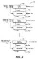
- FIG. 1illustrates a conventional electronics system 100 comprising a printed circuit (PC) board 102 , a system IC 104 , and a number of memory devices 106 .
- PC board 102may be a layered dielectric structure with internal and external wiring that allows system IC 104 and memory devices 106 to be mechanically supported and electrically connected internally to each other and to outside circuits and systems.
- Memory devices 106are discrete ICs such as four DRAM ICs of 512 kilobits (Kb) by 32 bits, which may be combined to provide 512 Kb by 128 bits.
- System IC 104may comprise, for example, a microprocessor or an application specific integrated circuit (ASIC) that utilizes memory devices 106 to store information.
- ASICapplication specific integrated circuit
- Each of memory devices 106 and system IC 104may be separately packaged in a suitable package formed of polymer or ceramic and having a plurality of input/output (I/O) pins for connection to PC board 102 .
- system 100provides certain advantages, such as ready testing of system IC 104 and memory devices 106 prior to their connection to PC board 102 and easy removal and replacement of faulty discrete components.
- system 100can be relatively large and may require more space than is available for many types of electronic devices such as cellular telephones, laptops, and personal digital assistants.
- FIG. 2is a block diagram of a conventional multi-chip module (MCM) 200 that integrates a number of raw chips (i.e., the silicon containing the integrated circuit—also referred to as a “die”) into a single semiconductor device.
- MCM 200comprises a system chip 202 and a number of memory chips 204 on a substrate 206 .
- System chip 202 and memory chips 204may correspond functionally to system IC 104 and memory devices 106 , respectively, of FIG. 1 , but are provided within a single, discrete package.
- MCM 200provides certain advantages, such as a reduction in the amount of space required for implementation and an increase in processing speeds due to shorter leads between chips.
- a multi-chip packaged semiconductor devicemay be viewed in terms of primary and secondary chips.
- a primary chiphas direct access to external connectors of the multi-chip package and can communicate or convey information directly through these external connectors to components or devices external to the multi-chip package.
- a primary chipmay comprise an application specific integrated circuit (ASIC) controller or microprocessor that performs the main system functions of the multi-chip package.
- System chip 202would also be an example of a primary chip.
- a secondary chipgenerally does not have direct access to external connectors and typically is utilized in concert with the primary chip to assist or enhance the primary chip's performance or functionality.
- a secondary chipmay comprise a memory subsystem, co-processor subsystem, analog subsystem, or other application-type specific subsystem.
- Memory chips 204would also be an example of secondary chips.
- secondary chipsgenerally are not able to “talk” or communicate directly through external connectors.
- a drawback of conventional multi-chip packaged semiconductor devices, such as MCM 200is that it does not allow complete testing of the secondary chips once they are incorporated into the package.
- memory chips 204are connected to system chip 202 , with system chip 202 connected to a number of I/O pins 208 of MCM 200 .
- No direct connectionsare available between memory chips 204 and external test equipment and, thus, a stringent final test of memory chips 204 within MCM 200 is not possible.
- KGDknown good die
- MCM 200Although is possible to test memory chips 204 by transferring data through other chips (e.g., system chip 202 ), this type of testing fails to detect all of the various types of memory failures. Specifically, external integrated circuit test equipment does not have direct access to the secondary chips because there are no pin-outs or other direct connections, because secondary chips interface through the primary chips. Consequently, a number of MCM failures are the result of integrated circuit chips that have not been fully tested. Often, these failures are not discovered until after incorporation into an electronic device, which adds to the cumulative cost of the defective MCM, not only for the MCM manufacturer, but also for their customers whose products fail to function properly due to the defective MCM. Thus, for complete testing and for quality and reliability reasons, direct access to secondary chips is required.
- the present inventionprovides a system and method that provides complete testing of one or more secondary chips within a multi-chip semiconductor device.
- a semiconductor memory chipfor packaging along with a system chip in a single semiconductor package having a plurality of external connectors.
- the memory chipincludes a memory storage array for storing data.
- a plurality of data buffersis provided for writing or reading data between said memory storage array and the system chip within the single semiconductor package.
- a first power levelmay be used for each of the plurality of data buffers.
- At least one test bufferis directly connected to certain of said plurality of external connectors for supporting testing of said memory chip within the single semiconductor package by external test equipment.
- a second power levelmay be used for the test buffer.
- a packaged semiconductor deviceincludes a plurality of external connectors for a semiconductor package.
- a primary chipdisposed within the semiconductor package, is connected to at least a portion of said plurality of external connectors.
- a secondary chipalso disposed within the semiconductor package, is connected to said primary chip.
- the secondary chipincludes a plurality of data signal drivers for transferring information between said secondary chip and said primary chip during a normal mode of operation.
- a first power levelmay be used for each of the plurality of data signal drivers.
- At least one test signal driveris directly connected to certain of said portion of said plurality of external connectors to provide testing of said secondary chip during a test mode of operation and while contained within the semiconductor package.
- a second power levelis may be for the test signal driver.
- a semiconductor chipfor incorporation as a secondary chip into a multi-chip packaged semiconductor device.
- the semiconductor chipincludes at least one data buffer operable to connect to a primary chip incorporated into the multi-chip packaged semiconductor device for receiving from and outputting signals to the primary chip during a normal mode of operation.
- a first power levelmay be used for each of the plurality of data buffers.
- a test bufferis operable to directly connect to an external terminal of the multi-chip packaged semiconductor device for receiving from and outputting signals to external testing circuitry during a test mode of operation.
- a second power levelmay be used for the test buffer.
- FIG. 1is a block diagram of a conventional electronic system.
- FIG. 2is a block diagram of a conventional multi-chip module.
- FIG. 3is a block diagram illustrating a multi-chip module 15 in accordance with an embodiment of the present invention.
- FIG. 4is a block diagram illustrating a buffer configuration in accordance with an embodiment of the present invention.
- FIG. 5is a schematic diagram, in partial block form, for an input/output buffer in accordance with an embodiment of the present invention.
- FIGS. 6A and 6Bare schematic diagrams for implementations of an output buffer in accordance with an embodiment of the present invention.
- FIG. 7is a block diagram illustrating a test buffer in 25 accordance with an embodiment of the present invention.
- FIG. 8is a schematic diagram for a test buffer in accordance with an embodiment of the present invention.
- FIG. 9is a block diagram illustrating a multi-chip module in accordance with an embodiment of the present invention.
- FIG. 10is a schematic diagram for a test buffer driver in accordance with an embodiment of the present invention.
- FIG. 11is a schematic diagram for a level translator circuit in accordance with an embodiment of the present invention.
- FIGS. 1 through 11 of the drawingsLike numerals are used for like and corresponding parts of the various drawings.
- the present inventionprovides systems and methods for testing one or more secondary chips within a multi-chip packaged semiconductor device.
- the secondary chipmay comprise any type of chip that lacks sufficient connections to external pins or terminals of the multi-chip package to allow complete testing of the secondary chip.
- a secondary chipmay comprise a memory subsystem, a co-processor subsystem, an analog subsystem, or other application-type specific subsystem.
- a secondary chip comprised of a memory chipis selected as an exemplary application in accordance with an embodiment of the present invention and described in detail below. However, it should be understood that the principles of the present invention are applicable for other types of secondary chips within a semiconductor package and are not limited to exemplary embodiments described herein.
- FIG. 3is a block diagram illustrating a multi-chip module (MCM) 300 in accordance with an embodiment of the present invention.
- MCM 300comprises a chip package 302 having a number of input/output (I/O) pins or terminals 306 , and containing a substrate 304 upon which a system chip 308 and a memory chip 310 are mounted.
- MCM 300may constitute a multi-chip semiconductor package i.e., a semiconductor device having multiple chips or dies contained within a single package.
- System chip 308may comprise, for example, a processor, a microprocessor, a microcontroller, a field programmable gate array, an ASIC, or any other type of chip or logic device that may communicate with a memory chip.
- Memory chip 310may comprise any type of memory such as, for example, random access memory (RAM) devices or read only memory (ROM) devices including static RAM (SRAM), dynamic RAM (DRAM), non-volatile RAM (NVRAM), programmable ROM (PROM), erasable programmable ROM (EPROM), electrically erasable programmable ROM (EEPROM), and flash memory.
- RAMrandom access memory
- ROMread only memory
- SRAMstatic RAM
- DRAMdynamic RAM
- NVRAMnon-volatile RAM
- PROMprogrammable ROM
- EPROMerasable programmable ROM
- EEPROMelectrically erasable programmable ROM
- System chip 308is shown as having a number of bonding pads 318 and bonding wires 316 which facilitate connections to substrate bonding pads 312 on substrate 304 and allow communication of information between system chip 308 and other chips or components within or external to MCM 300 .
- system chip 308communicates with memory chip 310 utilizing bonding pads 318 , bonding wires 316 , traces 314 , and memory bonding pads 320 .
- System chip 308also communicates with components outside of MCM 300 utilizing one or more connections such as through bonding pad 318 , bonding wire 316 , substrate bonding pad 312 , trace 328 , lead wire 326 , and terminal 306 .
- connection between system chip 308 and memory chip 310 and between system chip 308 and terminals 306may represent a common memory bus utilizing a four-layer substrate, with separate power supply planes for each chip.
- System chip 308may also have one or more input/output buffers or driver circuits 330 and 332 for receiving and driving the signals on the bonding pads 318 .
- buffer 330is used for communicating from die to die within MCM 300
- buffer 332is used for communicating with external components.
- system chip 308may use different voltage levels for communicating with memory chip 310 (i.e., from die-to-die within MCM 300 ) versus communicating with components outside of MCM 300 .
- a first power levele.g., 1.1V, 1.3V, 1.5V, or 1.8V
- a second power levele.g., 1.8V, 2.5V, or 3.3V
- memory chip 310comprises a number of input/output buffers 322 along with a test buffer 324 .
- Input/output buffers 322permit the reading and writing of data to memory chip 310 from system chip 308 .
- Each input/output buffer 322can be a single-bit buffer—i.e., a buffer which supports the input or output of only a single bit of data at a given time.
- Test buffer 324permits the direct testing of memory chip 310 by separately monitoring the data being read from memory chip 310 and providing this information directly to terminal 306 through traces 328 , 330 when MCM 300 is placed into a memory test mode (as described herein).
- Test buffer 324also can write information to memory chip 310 through input/output buffers 322 , as described in further detail below.
- a designated terminal 306is bonded to a particular bonding pad 318 of system chip 308 as well as to a particular memory bonding pad 320 utilized as the test input or test output pad for test buffer 324 .
- the memory bonding pads 320 that are utilized by test buffer 324do not connect directly to the substrate package memory bus that provides communication between memory chip 310 and system chip 308 .
- Test buffer 324may also be incorporated into one or more of the input/output buffers 322 such that one or more of the input/output buffers 322 also provides the test capabilities of test buffer 324 utilizing the principles of the present invention as described herein.
- one input/output buffer 322may incorporate test buffer 324 , with an additional memory bonding pad 320 utilized to input or output test data to one or more selected terminals 306 .
- test buffer 324Due to the incorporation of test buffer 324 and its direct connections to one or more terminals 306 of MCM 300 , memory chip 310 can be thoroughly tested after it has been packaged and contained inside MCM 300 . In particular, during normal operation, test buffer 324 is disabled (e.g., tri-stated) so that test buffer 324 does not interfere with the signals on one or more terminals 306 that are assigned to system chip 308 .
- test buffer 324transfers information through the designated terminals 306 .
- MCM 300will be placed into a memory test mode when a specified terminal 306 on MCM 300 is asserted or selected.
- the specified terminal 306may, for example, be an assigned test pin (i.e., a no-connect (NC) pin specifically used for memory test mode entry) or an input pin by which MCM 300 can recognize a test signal once a voltage level outside the normal operating range is established.
- Memory chip 310is then tested while inside MCM 300 by reassigning certain terminals 306 also used by system chip 308 as test input/output pins for memory chip 310 .
- the reassigned pinsmay then be used to provide addresses, input controls, data input/output signals, and other information to properly access and test memory chip 310 .
- one or more terminals 306may be designated as test pins to provide a test signal to place memory chip 310 into a test mode and also to provide control and/or test data signals.
- the test signal to place memory chip 310 into a test modemay be generated directly by system chip 308 without requiring a designated test pin to initiate testing.
- a specified voltage range or sequence of voltages at a certain terminal 306may initiate testing of memory chip 310 .
- a voltage-level sensormay monitor one or more of terminals 306 designated for system chip 308 and when a predetermined voltage level is detected, testing of the memory chip 310 is initiated.
- one or more of the above test initiation triggersprovides many options and test flexibility.
- MCM 300comprises a single memory chip 310 (e.g., a single DRAM) that is designed for in-package testing. It should be understood, however, that in other embodiments, multiple memory chips designed for in-package testing might also be employed utilizing the teachings of the present invention. If a single memory chip is provided, the test data bus and memory bus system may be optimized. For example, memory chip 310 may comprise a single, high-performance, synchronous DRAM of 512 Kb by 128 bits, with a wide test data bus and memory bus subsystem (used to communicate with system chip 308 ) having a width greater to or equal to 128 bits.
- memory chip 310may comprise a single, high-performance, synchronous DRAM of 512 Kb by 128 bits, with a wide test data bus and memory bus subsystem (used to communicate with system chip 308 ) having a width greater to or equal to 128 bits.
- memory chip 310may be configured as a 32, 64, 128, 256 bit, or greater size, with a bus width that is equivalent or greater in size to permit high-speed transfer of data between memory chip 310 and system chip 308 .
- embedded memoryi.e., memory integrated with other logic on a single die.
- memory chip 310may be manufactured, for example, using a standard commodity memory process, with the incorporation of the teachings of the present invention, while system chip 308 may be manufactured using a standard logic process or other types of processes.
- MCM 300is optimized for high performance chip-to-chip interface along with complete testing capability of the internal memory.
- MCM 300may comprise a standard ball grid array (BGA) or thin quad flatpack (TQFP) type of package having 144 pins or more.
- BGAball grid array
- TQFPthin quad flatpack
- the chip packagingmay be of various types of MCMs such as having a ceramic base with chips wire bonded (e.g., MCM-C) or employing thin film substrates (e.g., MCM-D), mounted on a silicon substrate (e.g., MCM-S), or mounted on a PCB substrate (e.g., MCM-L) such as a multi-chip package (MCP).
- MCM-Cceramic base with chips wire bonded
- MCM-Dthin film substrates
- MCM-Ssilicon substrate
- PCB substratee.g., MCM-L
- MCPmulti-chip package
- the packagingmay further utilize various surface mount technologies such as a single in-line package (SIP), dual in-line package (DIP), zig-zag in-line package (ZIP), plastic leaded chip carrier (PLCC), small outline package (SOP), thin SOP (TSOP), flatpack, and quad flatpack (QFP), to name but a few, and utilizing various leads (e.g., J-lead, gull-wing lead) or BGA type connectors.
- SIPsingle in-line package
- DIPdual in-line package
- ZIPzig-zag in-line package
- PLCCplastic leaded chip carrier
- SOPsmall outline package
- TSOPthin SOP
- QFPquad flatpack
- Vddqthe higher voltage level
- one test buffer 324is provided for every eight input/output buffers 322 to provide an eight-to-one data compression (e.g., data multiplexing) for testing purposes.
- data compressione.g., data multiplexing
- fewer test buffers 324 and terminals 306are required for testing of memory chip 310 .
- eight or more pinswould be required along with one test buffer 324 for every input/output buffer 322 .
- data compressionprovides more efficient use of external terminals 306 and minimizes the number of bonding pads and test buffers, along with associated circuitry, that is required to provide memory testing.
- Various data compression ratiosmay be selected, such as 2:1, 4:1, 8:1, 16:1, 32:1, 64:1, and 128:1. For example, for a 512 Kb by 128-bit memory and employing 16:1 compression, a minimum of eight test buffers and external terminal connections are required.
- multiple structuresmay be provided in MCM 300 or the chips contained therein to support the various voltage levels for power. This is because different voltage levels may be used for input/output (I/O) driving for operation and testing. For example, a first power level may be used for driving signals between chips, whereas a second power level may be used for testing of a chip. For such situations, the same I/O driving power level cannot be used for both chip-to-chip communication and testing because doing so would cause problems, such as latch-up.
- I/Oinput/output
- the first power level(which may be a lower voltage—e.g., 1.1V, 1.3V, 1.5V, or 1.8V) is used in the normal mode of operation for communicating signals to and from system chip 308
- the second power level(which may be a higher voltage—e.g., 1.8V, 2.5V, or 3.3V) is used in the test mode of operation for communicating signals to and from circuitry external to MCM 300
- the voltage on bonding pads 320 for input/output buffers 322may be at the first power level
- the voltage on the bonding pads 320 for test buffer 324may be at the second power level.
- MCM 300 and the chips contained thereinmay have circuitry and structures for supporting or translating between the various power levels, as further described herein.
- FIG. 4is a block diagram illustrating a buffer configuration 400 in accordance with an embodiment of the present invention.
- Buffer configuration 400is an exemplary buffer configuration that can be incorporated into a memory chip (such as memory chip 310 ) which is part of a multi-chip semiconductor package.
- Buffer configuration 400provides or supports memory test capability using standard memory test equipment while the memory chip is inside the multi-chip package.
- buffer configuration 400an eight-to-one data compression ratio is provided for testing of an exemplary 128 bit memory chip.
- Buffer configuration 400comprises 16 input/output buffers 402 and 16 test buffers 324 .
- Each input/output buffer 402represents eight single-bit input/output buffers. Therefore, with an 8:1 test data compression ratio, there is one test buffer 324 for every eight single-bit input/output buffers represented by input/output buffer 402 .
- test (Test) signalis provided to input/output buffers 402 and test buffers 324 to enable testing of the corresponding memory chip incorporating buffer configuration 400 .
- the test signalis used to place the memory chip into memory test mode.
- Test data input/output (TD 0 , TD 1 , . . . , TD 15 ) signalsare provided to respective test buffers 324 .
- TDIN 15signals are provided from corresponding test buffers 324 to respective input/output buffers 402 to communicate or convey, for example, test patterns designed to test the operation of the memory chip.
- Data read (DR) signalsare provided to input/output buffers 402 and respective test buffers 324 to communicate or convey data which is read from the memory chip for purposes of testing.
- Data write (DW) signalsare provided from input/output buffers 402 to communicate or convey data which is written into the memory chip for the purposes of testing.
- input/output buffers 402transfer data between the system chip through corresponding data (DR/DW) signals.
- Input/output buffers 402obtain data from the memory chip through data read (DR) signals and write to the memory chip through data write (DW) signals.
- a clock (CLK) signalmay be provided, if required, to synchronize the various buffer and data transfer operations.
- test data input/output (TD 0 , TD 1 , . . . , TD 15 ) signalsmay be at a higher power level (e.g., 1.8V, 2.5V, or 3.3V) while the other signals may be at the lower or core power level (e.g., 1.1V, 1.3V, 1.5V, or 1.8V).
- Input/output buffers 402 and test buffers 324have circuitry and structures for handling or translating between these various power levels.
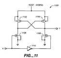
- a level translator circuit 1100may convert a signal at one power level to another power level.
- level translator circuit 1100comprises p-type transistors 1102 , 1104 , n-type transistors 1106 , 1108 , and an inverter gate 1110 .
- Each of transistors 1102 , 1104 , 1106 , and 1108are back-gate biased.
- a voltage source at one power level(either the high or low power level) is connected to the level translator circuit 1100 .
- level translator circuit 1100may receive signals at the other power level.
- One or more level translator circuits 1100may be incorporated and used throughout memory chip 310 or system chip 308 for translating between power levels (either from higher power level to lower power level, or vice versa).
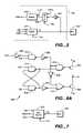
- FIG. 5is an exemplary schematic diagram, in partial block form, for an input/output buffer 402 in accordance with an embodiment of the present invention.
- input/output buffer 402comprises an output buffer 502 , an input buffer 504 , a multiplexer 506 , and a buffer 508 .
- Output buffer 502receives data read (DR) signals from the corresponding memory chip and prepares or temporarily stores the data prior to output through connections at memory bonding pad 320 .
- Various signalsare associated with output buffer 502 including test (Test) signal, data read (DR)/data write (DW) signals, and clock (CLK) as discussed above.
- An output enable (OE) signalmay also be provided for timing and initiation of data transfer.
- Data being written to input/output buffer 402passes through connections at memory bonding pad 320 and is received by input buffer 504 .
- Multiplexer 506receives the data (D) from input buffer 504 and/or test input data (TDIN) signals, (as controlled by the test signal), and transfers the data to buffer 508 , which may receive a clock (CLK) signal for synchronization. Buffer 508 then transfers to memory the data to be written via data write (DW) signal.
- Ddata
- TDINtest input data
- CLKclock
- FIG. 6Ais a schematic diagram for one implementation of output buffer 502 in accordance with an embodiment of the present invention.
- output buffer 502comprises inverters 602 , 606 , 608 , and 618 , NAND gates 604 , 610 , 614 , and 616 , NOR gate 612 , along with p-type and n-type transistors 620 , 622 , respectively.
- Output buffer 502receives test (Test) signal, output enable (OE) signal, data read (DR) signal and its complement (DR*) signal, and may also receive a clock signal (not shown) for synchronization.
- Output buffer 502functions to provide the data to the memory bus when a memory read operation is performed. When the memory chip is being tested and receives the test signal, output buffer 502 inhibits the output of the data (D) so as to not interfere with memory testing being performed.
- test signalis inverted by inverter 602 and received by NAND gate 604 along with output enable (OE) signal. If the test signal is at a “logic high” signal level, the memory chip is placed in memory test mode. NAND gate 604 outputs a “logic high” signal level, which is inverted by inverter 606 into a “logic low” signal level. This results in NAND gate 610 providing a “logic high” signal level that turns transistor 620 off. The “logic low” signal level from inverter 606 is inverted by inverter 608 into a “logic high” signal level. This results in NOR gate 612 providing a “logic low” signal level to transistor 622 . Accordingly, transistor 622 switches off so that no data (D) passes through output buffer 502 .
- OEoutput enable
- test signalis at a “logic low” signal level
- the memory chipis in normal operation (i.e., no initiation of memory testing).
- output enable (OE) signalis at a “logic high” signal level
- NAND gate 604supplies a “logic low” signal level, which results in NAND gate 610 receiving a “logic high” signal level and NOR gate 612 receiving a “logic low” signal level.
- Thisallows the value of the data (DR and DR*) to determine whether to switch on or off transistors 620 and 622 , thus allowing them to function as an output driver circuit. Accordingly, data is permitted to be transferred through output buffer 502 .
- inverters 602 , 606 , and 608 along with NAND gate 610 and NOR gate 612implement tri-state circuitry that is utilized to enable or disable output buffer 502 .
- NAND gates 614 , 616which are cross-coupled together to function as latches, receive data signals DR, DR*. If DR is at a “logic high” signal level, NAND gate 616 provides a “logic low” signal level, which gets inverted by inverter 618 , while NAND gate 614 provides a “logic high” signal level. Consequently, NOR gate 612 receives a “logic high” signal level, which results in transistor 622 being switched off. NAND gate 610 receives a “logic high” signal level from inverter 606 and NAND gate 614 , which results in transistor 620 being switched on. Thus, a “logic high” signal level is provided as an output data signal when DR is at a “logic high” signal level. Similarly, if DR is at a “logic low” signal level, transistor 620 is switched off and transistor 622 is switched on to provide a “logic low” signal level as an output data signal.
- FIG. 6Bis a schematic diagram for another implementation of output buffer 502 in accordance with an embodiment of the present invention.
- This implementation depicted in FIG. 6Bis similar in many respects to the implementation depicted in FIG. 6A .
- output buffer 502comprises inverters 624 , 626 , 628 , 630 , 632 , 634 , 636 , 638 , 640 , 642 , and 644 , DQ flip-flops 650 and 652 , NOR gates 654 and 656 , NAND gate 658 , multiplexer 660 , pass gate circuits 670 , 672 , 674 , 676 , 678 , 680 , 682 , and 684 , level translator circuits 686 and 688 , p-type transistor 690 , and n-type transistor 692 .
- Level translator circuits 686 and 688function to translate signals from one power level (e.g., 1.1V, 1.3V, 1.5V, or 1.8V) to another power level (e.g., 1.8V, 2.5V, or 3.3V) between input and output of the buffer 502 .
- One power levele.g., 1.1V, 1.3V, 1.5V, or 1.8V
- another power levele.g., 1.8V, 2.5V, or 3.3V
- Each pass gate circuit 670 , 672 , 674 , 676 , 678 , 680 , 682 , and 684generally functions to pass the value of a signal appearing at its input as the value of its output signal upon a particular value for some “pass” signal (which, as shown, can be an INV signal or a BYPS signal).
- An exemplary implementation of a pass gate circuitis described in related U.S. application Ser. No. 09/967,389 entitled “Testing of Integrated Circuit Devices,” filed on Sep. 28, 2001, to be issued as U.S. Pat. No. 6,754,866 on Jun. 22, 2004, assigned to the same assignee and incorporated by reference herein in its entirety.
- FIG. 7is a block diagram illustrating an exemplary test buffer 324 in accordance with an embodiment of the present invention.
- Test buffer 324may be incorporated into a memory chip that is incorporated into a multi-chip-semiconductor package to provide memory test capability using standard memory test equipment.
- Test buffer 324utilizes one or more bonding pads 320 to transfer information, via test data input/output (TD) signal, through external connections of multi-chip module 300 .
- Test data input/output (TD) signalmay convey or communicate test data, memory addresses, control signals, and various other information required to test the memory chip.
- Test buffer 324also receives test (Test) signal, which enables testing of the corresponding memory chip, along with the data read (DR) signals that are utilized during memory testing.
- Testtest
- a clock (CLK) signalmay also be provided, if required to synchronize the operations or provide other clocking functions.
- Test input data (TDIN) signalsare provided by the test buffer 324 to the respective input/output buffers of the memory chip in order to write various test data into the memory chip to ensure correct operation.
- FIG. 8is an exemplary schematic diagram for a test buffer 324 in accordance with an embodiment of the present invention.
- Test buffer 324comprises a number of NOR gates 810 , 812 , 814 , and 816 that receive data read (DRO–DR 7 ) signals and output the logical result to NAND gate 820 .
- NOR gates 802 , 804 , 806 , and 808receive complements of the data read (DRO*–DR 7 *) signals and output the logical result to NAND gate 818 .
- NAND gates 818 , 820output their result to transistors 826 , 828 and transistors 830 , 832 , respectively.
- Transistor 826 , 828 and transistors 830 , 832function as pass gates controlled by the complement of a data latch signal (DLAT*) in conjunction with inverters 822 , 824 .
- the pass gatesprovide the signals output by NAND gates 818 and 820 to pairs of inverters 834 , 836 and 838 , 840 . These inverter pairs function as data latches.
- the output of the latch formed by inverters 834 , 836is fed to a NAND gate 846 , while the output of the latch formed by inverters 838 , 840 is inverted by an inverter 856 and fed to a NOR gate 850 .
- the output signal of NAND gate 846controls a p-type transistor 856
- the output signal of NAND gate 850controls an n-type transistor 854 .
- Transistors 852 , 854form an output driver circuit to provide the output for test data (TD) input/output signal.
- Input buffer 856 and inverters 858 , 860receive externally provided test data signals and provide this data to respective input/output buffers of the memory chip, as described above.
- a NAND gate 842 , inverters 844 , 848 , NAND gate 846 , and NOR gate 850implement the tri-state circuitry that is utilized to enable or disable test buffer 324 . For example, if test signal and OE signal are not both at a “logic high” signal level, NAND gate 842 provides a “logic high” signal level, which is inverted to a “logic low” signal level by inverter 844 . A “logic low” signal level at NAND gate 846 results in a “logic high” signal level output, which switches transistor 852 off.
- Inverter 848inverts the “logic low” signal level from inverter 844 , which results in NOR gate 850 producing a “logic low” signal level that switches transistor 854 off also. Thus, test buffer 324 does not produce an output that would interfere with other memory functions when the memory chip is in normal operation.
- test buffer 324when test and output enable (OE) signals are both at a “logic high” signal level. If data read (DR) signals are all at a “logic low” signal level, the outputs of NAND gates 820 , 818 are at a “logic low” and “logic high” signal level, respectively. This results in NOR gate 850 and NAND gate 846 generating “logic high” signal levels, which switches on transistor 854 and switches off transistor 852 to output a “logic low” TD signal level. If data read (DR) signals are all at a “logic high” signal level, the outputs of NAND gates- 820 , 818 are at a “logic high” and “logic low” signal levels, respectively. This results in NOR gate 850 and NAND gate 846 generating “logic low” signal levels, which switches transistors 852 , 854 on and off, respectively, to output a “logic high” signal level for TD signal.
- FIG. 9is a block diagram illustrating a multi-chip module (MCM) 900 in accordance with an embodiment of the present invention.
- MCM 900illustrates a system and method of providing control signals to a secondary chip such as memory chip 310 that typically would not have direct access to external pins or connectors such as terminals 306 .
- MCM 900comprises similar elements as MCM 300 , described in detail in reference to FIG. 3 , and therefore the description for the common elements will not be repeated here.
- the various unique elements of MCM 900which were not shown in MCM 300 , may be incorporated into MCM 300 or work in conjunction with elements of MCM 300 , as described in further detail below.
- MCM 900comprises system chip 308 and memory chip 310 .
- System chip 308comprises an output buffer 340 that provides control or logic signals such as, for example, address decode signals. These signals may be communicated through the connections shown to an input buffer 352 that receives these signals and provides them to memory chip 310 , which takes the appropriate action based on the control or logic signals.
- memory chip 310may provide data that is stored in certain memory locations identified by the control or logic signals.
- Memory chip 310further comprises a test buffer driver 350 that can receive control or logic signals through one or more terminals 306 .
- Test buffer driver 350may share these terminals 306 with system chip 308 (as shown in FIG. 9 ) or may utilize certain of terminals 306 that are dedicated for test purposes, as similarly explained in detail above for test buffer 324 .
- Test buffer driver 350receives these control or logic signals from external test equipment through terminals 306 and provides these signals to input buffer 352 of memory chip 310 . Consequently, memory chip 310 can be controlled either by system chip 308 or by test buffer driver 350 .
- FIG. 10is a schematic diagram for test buffer driver 350 in accordance with an embodiment of the present invention.
- Test buffer driver 350may be incorporated into test buffer 324 , but multiplexing of signals or similar methods would be required if the same input/output terminals 306 are utilized for control or logic signals along with data input and output signals.
- one or more separate terminals 306may be assigned for control and logic signals (e.g., command and control type signals such as addressing information) and other terminals 306 for data input and output signals (e.g., test data).
- test buffer driver 350is connected to input buffer 352 of memory chip 310 , with this connection shared by system chip 308 .
- system chip 308may use this connection to provide control signals to memory chip 310 through input buffer 352 .
- this connectionis used by test buffer driver 350 to provide control signals to memory chip 310 through input buffer 352 .
- input buffer 352may be incorporated into input/output buffer 322 of memory chip 310 .
- test buffer driver 350comprises resistors 1002 and 1014 , inverter 1004 , p-type transistors 1006 and 1008 , and n-type transistors 1010 and 1012 .
- Resistors 1002 and 1014provide input protection and isolation for test buffer driver 350 .
- Test signalis at a “logic low” signal level
- transistors 1006 and 1012are switched off and test buffer driver 350 does not provide any output or control signal to input buffer 352 , and thus does not affect circuit operation of memory chip 310 .
- Test signalis at a “logic high” signal level, then transistors 1006 and 1012 are switched on.
- control signals(CS) to be driven by transistors 1008 and 1010 to input buffer 352 of memory chip 310 .
- An invertermay be included at the input to test buffer driver 350 so that when control signals are at a “logic low” or “logic high” level, then the output of test buffer driver 350 are also at a “logic low” or “logic high” level, respectively.
- the present inventionprovides many advantages over conventional multi-chip packaged semiconductor devices by providing the ability to stringently test the secondary chip (e.g., memory chip) inside the package using standard integrated circuit test equipment (e.g., memory test equipment). Furthermore, the ability to stringently test the secondary chips provides many advantages. For example, one or more memory chips may be provided having a wide data input/output configuration that is optimally tailored to the system data bus architecture within the package.
- the present inventionis not limited to the testing of memory chips within a multi-chip package.
- One or more exemplary embodiments described aboveutilized one or more memory chips as the exemplary secondary chips, but the present invention is not limited to these embodiments.
- the principles of the present inventionare applicable to other types of secondary chips such as co-processors, analog chips, or various types of application specific chips or subsystems that interface through primary chips or fail to interface directly through external connectors of the multi-chip package.
- one or more devicessuch as, for example, signal drivers (i.e., current or voltage signal drivers), may replace the data buffers and/or test buffers.
- the primary chipmay comprise an ASIC and the secondary chip may comprise a co-processor, with control signals and data passing between the interface of the primary and secondary chip through signal drivers that may be accompanied by or include buffers or registers.
- the signal drivers or interfacemay comprise, for example, transistor-to-transistor logic (TTL), low-voltage TTL (LVTTL), or stub series terminated logic (SSTL) interface technology.
Landscapes
- Tests Of Electronic Circuits (AREA)
Abstract
Description
Claims (24)
Priority Applications (2)
| Application Number | Priority Date | Filing Date | Title |
|---|---|---|---|
| US10/877,687US7240254B2 (en) | 2000-09-21 | 2004-06-25 | Multiple power levels for a chip within a multi-chip semiconductor package |
| US11/207,518US7444575B2 (en) | 2000-09-21 | 2005-08-19 | Architecture and method for testing of an integrated circuit device |
Applications Claiming Priority (3)
| Application Number | Priority Date | Filing Date | Title |
|---|---|---|---|
| US09/666,208US6732304B1 (en) | 2000-09-21 | 2000-09-21 | Chip testing within a multi-chip semiconductor package |
| US10/824,734US7139945B2 (en) | 2000-09-21 | 2004-04-15 | Chip testing within a multi-chip semiconductor package |
| US10/877,687US7240254B2 (en) | 2000-09-21 | 2004-06-25 | Multiple power levels for a chip within a multi-chip semiconductor package |
Related Parent Applications (2)
| Application Number | Title | Priority Date | Filing Date |
|---|---|---|---|
| US09/666,208Continuation-In-PartUS6732304B1 (en) | 2000-09-21 | 2000-09-21 | Chip testing within a multi-chip semiconductor package |
| US10/824,734Continuation-In-PartUS7139945B2 (en) | 2000-09-21 | 2004-04-15 | Chip testing within a multi-chip semiconductor package |
Related Child Applications (1)
| Application Number | Title | Priority Date | Filing Date |
|---|---|---|---|
| US11/207,518Continuation-In-PartUS7444575B2 (en) | 2000-09-21 | 2005-08-19 | Architecture and method for testing of an integrated circuit device |
Publications (2)
| Publication Number | Publication Date |
|---|---|
| US20050024977A1 US20050024977A1 (en) | 2005-02-03 |
| US7240254B2true US7240254B2 (en) | 2007-07-03 |
Family
ID=34108169
Family Applications (1)
| Application Number | Title | Priority Date | Filing Date |
|---|---|---|---|
| US10/877,687Expired - Fee RelatedUS7240254B2 (en) | 2000-09-21 | 2004-06-25 | Multiple power levels for a chip within a multi-chip semiconductor package |
Country Status (1)
| Country | Link |
|---|---|
| US (1) | US7240254B2 (en) |
Cited By (14)
| Publication number | Priority date | Publication date | Assignee | Title |
|---|---|---|---|---|
| US20070067687A1 (en)* | 2001-09-28 | 2007-03-22 | Ong Adrian E | Integrated Circuit Testing Module Configured for Set-up and Hold Time Testing |
| US20070079204A1 (en)* | 2001-09-28 | 2007-04-05 | Ong Adrian E | Integrated Circuit Testing Module Including Signal Shaping Interface |
| US20070168808A1 (en)* | 2001-09-28 | 2007-07-19 | Inapac Technology, Inc. | Integrated circuit testing module including data compression |
| US20070263458A1 (en)* | 2006-05-04 | 2007-11-15 | Ong Adrian E | Memory Device Including Multiplexed Inputs |
| US20080089139A1 (en)* | 2006-10-03 | 2008-04-17 | Inapac Technology, Inc. | Memory accessing circuit system |
| US20080263415A1 (en)* | 2007-04-17 | 2008-10-23 | Bernhard Ruf | Integrated Circuit, Memory Module, Method of Operating an Integrated Circuit, Method of Fabricating an Integrated Circuit, Computer Program Product, and Computing System |
| US20100228514A1 (en)* | 2006-06-30 | 2010-09-09 | Rambus Inc. | Delay lock loop delay adjusting method and apparatus |
| US20110202789A1 (en)* | 2005-08-18 | 2011-08-18 | Rambus Inc. | Processor-memory unit for use in system-in-package and system-in-module devices |
| US8063650B2 (en) | 2002-11-27 | 2011-11-22 | Rambus Inc. | Testing fuse configurations in semiconductor devices |
| US8286046B2 (en) | 2001-09-28 | 2012-10-09 | Rambus Inc. | Integrated circuit testing module including signal shaping interface |
| US20160086920A1 (en)* | 2014-09-22 | 2016-03-24 | SK Hynix Inc. | Semiconductor devices and semiconductor systems including the same |
| US20230060343A1 (en)* | 2021-08-30 | 2023-03-02 | Murata Manufacturing Co., Ltd. | Electrical device comprising an ac voltage divider and capacitors arranged in integrated components |
| US20230119193A1 (en)* | 2021-10-18 | 2023-04-20 | Board Of Trustees Of The University Of Arkansas | High-temperature power module integrated with an optically galvanic isolated gate driver |
| US20250167679A1 (en)* | 2023-11-20 | 2025-05-22 | Stmicroelectronics International N.V. | Circuit and method for reducing driving losses in gan switches |
Families Citing this family (14)
| Publication number | Priority date | Publication date | Assignee | Title |
|---|---|---|---|---|
| US7404117B2 (en)* | 2005-10-24 | 2008-07-22 | Inapac Technology, Inc. | Component testing and recovery |
| US7245141B2 (en) | 2002-11-27 | 2007-07-17 | Inapac Technology, Inc. | Shared bond pad for testing a memory within a packaged semiconductor device |
| US7309999B2 (en) | 2002-11-27 | 2007-12-18 | Inapac Technology, Inc. | Electronic device having an interface supported testing mode |
| US7466160B2 (en)* | 2002-11-27 | 2008-12-16 | Inapac Technology, Inc. | Shared memory bus architecture for system with processor and memory units |
| US7424659B2 (en)* | 2003-10-31 | 2008-09-09 | Sandisk Il Ltd. | System-in-package and method of testing thereof |
| US7518231B2 (en)* | 2005-08-15 | 2009-04-14 | Infineon Technologies Ag | Differential chip performance within a multi-chip package |
| US7779311B2 (en)* | 2005-10-24 | 2010-08-17 | Rambus Inc. | Testing and recovery in a multilayer device |
| US7561027B2 (en)* | 2006-10-26 | 2009-07-14 | Hewlett-Packard Development Company, L.P. | Sensing device |
| US7665003B2 (en)* | 2006-12-15 | 2010-02-16 | Qualcomm Incorporated | Method and device for testing memory |
| US9405339B1 (en)* | 2007-04-30 | 2016-08-02 | Hewlett Packard Enterprise Development Lp | Power controller |
| CN203809329U (en)* | 2014-04-14 | 2014-09-03 | 江苏多维科技有限公司 | Direct-current fan control chip |
| JP2019168755A (en) | 2018-03-22 | 2019-10-03 | 東芝メモリ株式会社 | Memory system, power supply control circuit and control method |
| KR20210119678A (en)* | 2020-03-25 | 2021-10-06 | 에스케이하이닉스 주식회사 | Multi-Chip Package and Method of Testing The Same |
| CN114121082B (en)* | 2020-08-26 | 2024-12-06 | 长鑫存储技术(上海)有限公司 | Transmission circuit, interface circuit and memory |
Citations (74)
| Publication number | Priority date | Publication date | Assignee | Title |
|---|---|---|---|---|
| US4263650A (en) | 1974-10-30 | 1981-04-21 | Motorola, Inc. | Digital data processing system with interface adaptor having programmable, monitorable control register therein |
| US4743841A (en) | 1985-05-20 | 1988-05-10 | Fujitsu Limited | Semiconductor integrated circuit including circuit elements evaluating the same and having means for testing the circuit elements |
| US4773028A (en) | 1984-10-01 | 1988-09-20 | Tektronix, Inc. | Method and apparatus for improved monitoring and detection of improper device operation |
| US4825414A (en) | 1987-06-30 | 1989-04-25 | Fujitsu Limited | Semiconductor integrated circuit device having gate array and memory and input-output buffer |
| US4873669A (en) | 1986-07-30 | 1989-10-10 | Mitsubishi Denki Kabushiki Kaisha | Random access memory device operable in a normal mode and in a test mode |
| US5151881A (en) | 1987-04-24 | 1992-09-29 | Hitachi, Ltd. | Semiconductor memory including an arrangement to permit external monitoring of an internal control signal |
| US5251095A (en) | 1992-07-31 | 1993-10-05 | International Business Machines Corporation | Low temperature conduction module for a cryogenically-cooled processor |
| US5301156A (en) | 1991-07-18 | 1994-04-05 | Hewlett-Packard Company | Configurable self-test for embedded RAMs |
| US5326428A (en) | 1993-09-03 | 1994-07-05 | Micron Semiconductor, Inc. | Method for testing semiconductor circuitry for operability and method of forming apparatus for testing semiconductor circuitry for operability |
| US5388104A (en) | 1990-12-27 | 1995-02-07 | Kabushiki Kaisha Toshiba | Semiconductor integrated circuit capable of testing memory blocks |
| US5418452A (en) | 1993-03-25 | 1995-05-23 | Fujitsu Limited | Apparatus for testing integrated circuits using time division multiplexing |
| US5457400A (en) | 1992-04-10 | 1995-10-10 | Micron Technology, Inc. | Semiconductor array having built-in test circuit for wafer level testing |
| US5477545A (en) | 1993-02-09 | 1995-12-19 | Lsi Logic Corporation | Method and apparatus for testing of core-cell based integrated circuits |
| US5479105A (en) | 1993-06-25 | 1995-12-26 | Samsung Electronics Co., Ltd. | Known-good die testing apparatus |
| US5506499A (en) | 1995-06-05 | 1996-04-09 | Neomagic Corp. | Multiple probing of an auxilary test pad which allows for reliable bonding to a primary bonding pad |
| US5535165A (en) | 1995-06-30 | 1996-07-09 | Cirrus Logic, Inc. | Circuits, systems and methods for testing integrated circuit devices including logic and memory circuitry |
| US5594694A (en) | 1995-07-28 | 1997-01-14 | Micron Quantum Devices, Inc. | Memory circuit with switch for selectively connecting an input/output pad directly to a nonvolatile memory cell |
| US5604432A (en) | 1992-04-23 | 1997-02-18 | Intel Corporation | Test access architecture for testing of circuits modules at an intermediate node within an integrated circuit chip |
| US5619461A (en) | 1995-07-28 | 1997-04-08 | Micron Quantum Devices, Inc. | Memory system having internal state monitoring circuit |
| US5657284A (en) | 1995-09-19 | 1997-08-12 | Micron Technology, Inc. | Apparatus and method for testing for defects between memory cells in packaged semiconductor memory devices |
| US5677885A (en) | 1995-11-28 | 1997-10-14 | Micron Quantum Devices, Inc. | Memory system with non-volatile data storage unit and method of initializing same |
| US5719438A (en) | 1994-09-28 | 1998-02-17 | International Business Machines Corporation | Method and workpiece for connecting a thin layer to a monolithic electronic module's surface and associated module packaging |
| US5751987A (en)* | 1990-03-16 | 1998-05-12 | Texas Instruments Incorporated | Distributed processing memory chip with embedded logic having both data memory and broadcast memory |
| US5751015A (en) | 1995-11-17 | 1998-05-12 | Micron Technology, Inc. | Semiconductor reliability test chip |
| US5801452A (en) | 1996-10-25 | 1998-09-01 | Micron Technology, Inc. | Multi chip module including semiconductor wafer or dice, interconnect substrate, and alignment member |
| US5805609A (en) | 1995-06-07 | 1998-09-08 | Samsung Electronics Co., Ltd. | Method and apparatus for testing a megacell in an ASIC using JTAG |
| US5807762A (en) | 1996-03-12 | 1998-09-15 | Micron Technology, Inc. | Multi-chip module system and method of fabrication |
| US5825782A (en)* | 1996-01-22 | 1998-10-20 | Micron Technology, Inc. | Non-volatile memory system including apparatus for testing memory elements by writing and verifying data patterns |
| US5825697A (en) | 1995-12-22 | 1998-10-20 | Micron Technology, Inc. | Circuit and method for enabling a function in a multiple memory device module |
| US5923600A (en) | 1996-10-02 | 1999-07-13 | Kabushiki Kaisha Toshiba | Semiconductor device and test method and apparatus for semiconductor device |
| US5925142A (en) | 1995-10-06 | 1999-07-20 | Micron Technology, Inc. | Self-test RAM using external synchronous clock |
| US5966388A (en) | 1997-01-06 | 1999-10-12 | Micron Technology, Inc. | High-speed test system for a memory device |
| US5995379A (en) | 1997-10-30 | 1999-11-30 | Nec Corporation | Stacked module and substrate therefore |
| US6011720A (en) | 1998-01-13 | 2000-01-04 | Mitsubishi Denki Kabushiki Kaisha | Nonvolatile memory with reduced write time/write verify time and semiconductor device thereof |
| US6026039A (en) | 1997-12-20 | 2000-02-15 | Samsung Electronics Co., Ltd. | Parallel test circuit for semiconductor memory |
| US6047393A (en) | 1997-06-13 | 2000-04-04 | Advantest Corporation | Memory testing apparatus |
| US6069483A (en) | 1997-12-16 | 2000-05-30 | Intel Corporation | Pickup chuck for multichip modules |
| US6072326A (en) | 1997-08-22 | 2000-06-06 | Micron Technology, Inc. | System for testing semiconductor components |
| US6100716A (en)* | 1998-09-17 | 2000-08-08 | Nortel Networks Corporation | Voltage excursion detection apparatus |
| US6100708A (en) | 1997-09-26 | 2000-08-08 | Mitsubishi Denki Kabushiki Kaisha | Probe card and wafer testing method using the same |
| US6104658A (en) | 1996-08-08 | 2000-08-15 | Neomagic Corporation | Distributed DRAM refreshing |
| US6137167A (en) | 1998-11-24 | 2000-10-24 | Micron Technology, Inc. | Multichip module with built in repeaters and method |
| US6188232B1 (en) | 1996-12-31 | 2001-02-13 | Micron Technology, Inc. | Temporary package, system, and method for testing semiconductor dice and chip scale packages |
| US6191603B1 (en) | 1999-01-08 | 2001-02-20 | Agilent Technologies Inc. | Modular embedded test system for use in integrated circuits |
| US6194738B1 (en) | 1996-06-13 | 2001-02-27 | Micron Technology, Inc. | Method and apparatus for storage of test results within an integrated circuit |
| US6216241B1 (en) | 1998-10-08 | 2001-04-10 | Agere Systems Guardian Corp. | Method and system for testing multiport memories |
| US6263463B1 (en) | 1996-05-10 | 2001-07-17 | Advantest Corporation | Timing adjustment circuit for semiconductor test system |
| US6274937B1 (en) | 1999-02-01 | 2001-08-14 | Micron Technology, Inc. | Silicon multi-chip module packaging with integrated passive components and method of making |
| US6286115B1 (en) | 1998-06-29 | 2001-09-04 | Micron Technology, Inc. | On-chip testing circuit and method for integrated circuits |
| US6294839B1 (en) | 1999-08-30 | 2001-09-25 | Micron Technology, Inc. | Apparatus and methods of packaging and testing die |
| US6298001B1 (en) | 1995-04-24 | 2001-10-02 | Samsung Electronics Co., Ltd. | Semiconductor memory device enabling direct current voltage test in package status |
| US6300782B1 (en) | 1999-05-03 | 2001-10-09 | Micron Technology, Inc. | System for testing semiconductor components having flexible interconnect |
| US6310484B1 (en) | 1996-04-01 | 2001-10-30 | Micron Technology, Inc. | Semiconductor test interconnect with variable flexure contacts |
| USRE37611E1 (en) | 1996-01-22 | 2002-03-26 | Micron Technology, Inc. | Non-volatile memory system having internal data verification test mode |
| US6366487B1 (en) | 1998-12-30 | 2002-04-02 | Samsung Electronics Co., Ltd. | Plurality of integrated circuit chips |
| US6392948B1 (en) | 1996-08-29 | 2002-05-21 | Micron Technology, Inc. | Semiconductor device with self refresh test mode |
| US6396291B1 (en) | 1999-04-23 | 2002-05-28 | Micron Technology, Inc. | Method for testing semiconductor components |
| US6407566B1 (en) | 2000-04-06 | 2002-06-18 | Micron Technology, Inc. | Test module for multi-chip module simulation testing of integrated circuit packages |
| US6441479B1 (en) | 2000-03-02 | 2002-08-27 | Micron Technology, Inc. | System-on-a-chip with multi-layered metallized through-hole interconnection |
| US20020117729A1 (en) | 2001-01-30 | 2002-08-29 | Kiyoshi Aiki | Semiconductor integrated circuit device |
| US6445625B1 (en) | 2000-08-25 | 2002-09-03 | Micron Technology, Inc. | Memory device redundancy selection having test inputs |
| US6456099B1 (en) | 1998-12-31 | 2002-09-24 | Formfactor, Inc. | Special contact points for accessing internal circuitry of an integrated circuit |
| US6470484B1 (en) | 2000-05-18 | 2002-10-22 | Lsi Logic Corporation | System and method for efficient layout of functionally extraneous cells |
| US6472747B2 (en) | 2001-03-02 | 2002-10-29 | Qualcomm Incorporated | Mixed analog and digital integrated circuits |
| US6484279B2 (en) | 1998-01-21 | 2002-11-19 | Micron Technology, Inc. | Testing system for evaluating integrated circuits, a testing system, and a method for testing an integrated circuit |
| US6483760B2 (en) | 2000-07-20 | 2002-11-19 | Samsung Electronics Co., Ltd. | Semiconductor memory integrated circuit operating at different test modes |
| US6507885B2 (en) | 1996-10-29 | 2003-01-14 | Micron Technology, Inc. | Memory system, method and predecoding circuit operable in different modes for selectively accessing multiple blocks of memory cells for simultaneous writing or erasure |
| US6519725B1 (en) | 1997-03-04 | 2003-02-11 | International Business Machines Corporation | Diagnosis of RAMS using functional patterns |
| US6519171B2 (en) | 2000-11-17 | 2003-02-11 | Fujitsu Limited | Semiconductor device and multichip module |
| US6732304B1 (en)* | 2000-09-21 | 2004-05-04 | Inapac Technology, Inc. | Chip testing within a multi-chip semiconductor package |
| US6791175B2 (en) | 2001-09-29 | 2004-09-14 | Kabushiki Kaisha Toshiba | Stacked type semiconductor device |
| US6801461B2 (en) | 1996-04-30 | 2004-10-05 | Texas Instruments Incorporated | Built-in self-test arrangement for integrated circuit memory devices |
| US20040232559A1 (en) | 2003-05-19 | 2004-11-25 | Adelmann Todd C. | Interconnect method for directly connected stacked integrated circuits |
| US6996754B1 (en) | 1999-09-27 | 2006-02-07 | Samsung Electronics Company Limited | Integrated circuit device having an internal state monitoring function |
- 2004
- 2004-06-25USUS10/877,687patent/US7240254B2/ennot_activeExpired - Fee Related
Patent Citations (88)
| Publication number | Priority date | Publication date | Assignee | Title |
|---|---|---|---|---|
| US4263650B1 (en) | 1974-10-30 | 1994-11-29 | Motorola Inc | Digital data processing system with interface adaptor having programmable monitorable control register therein |
| US4263650A (en) | 1974-10-30 | 1981-04-21 | Motorola, Inc. | Digital data processing system with interface adaptor having programmable, monitorable control register therein |
| US4773028A (en) | 1984-10-01 | 1988-09-20 | Tektronix, Inc. | Method and apparatus for improved monitoring and detection of improper device operation |
| US4743841A (en) | 1985-05-20 | 1988-05-10 | Fujitsu Limited | Semiconductor integrated circuit including circuit elements evaluating the same and having means for testing the circuit elements |
| US4873669A (en) | 1986-07-30 | 1989-10-10 | Mitsubishi Denki Kabushiki Kaisha | Random access memory device operable in a normal mode and in a test mode |
| US5151881A (en) | 1987-04-24 | 1992-09-29 | Hitachi, Ltd. | Semiconductor memory including an arrangement to permit external monitoring of an internal control signal |
| US4825414A (en) | 1987-06-30 | 1989-04-25 | Fujitsu Limited | Semiconductor integrated circuit device having gate array and memory and input-output buffer |
| US5751987A (en)* | 1990-03-16 | 1998-05-12 | Texas Instruments Incorporated | Distributed processing memory chip with embedded logic having both data memory and broadcast memory |
| US5388104A (en) | 1990-12-27 | 1995-02-07 | Kabushiki Kaisha Toshiba | Semiconductor integrated circuit capable of testing memory blocks |
| US5301156A (en) | 1991-07-18 | 1994-04-05 | Hewlett-Packard Company | Configurable self-test for embedded RAMs |
| US5457400A (en) | 1992-04-10 | 1995-10-10 | Micron Technology, Inc. | Semiconductor array having built-in test circuit for wafer level testing |
| US5604432A (en) | 1992-04-23 | 1997-02-18 | Intel Corporation | Test access architecture for testing of circuits modules at an intermediate node within an integrated circuit chip |
| US5251095A (en) | 1992-07-31 | 1993-10-05 | International Business Machines Corporation | Low temperature conduction module for a cryogenically-cooled processor |
| US5477545A (en) | 1993-02-09 | 1995-12-19 | Lsi Logic Corporation | Method and apparatus for testing of core-cell based integrated circuits |
| US5418452A (en) | 1993-03-25 | 1995-05-23 | Fujitsu Limited | Apparatus for testing integrated circuits using time division multiplexing |
| US5479105A (en) | 1993-06-25 | 1995-12-26 | Samsung Electronics Co., Ltd. | Known-good die testing apparatus |
| US5523697A (en) | 1993-09-03 | 1996-06-04 | Micron Technology, Inc. | Testing apparatus for engaging electrically conductive test pads on a semiconductor substrate having integrated circuitry for operability testing thereof |
| US5326428A (en) | 1993-09-03 | 1994-07-05 | Micron Semiconductor, Inc. | Method for testing semiconductor circuitry for operability and method of forming apparatus for testing semiconductor circuitry for operability |
| US5719438A (en) | 1994-09-28 | 1998-02-17 | International Business Machines Corporation | Method and workpiece for connecting a thin layer to a monolithic electronic module's surface and associated module packaging |
| US6298001B1 (en) | 1995-04-24 | 2001-10-02 | Samsung Electronics Co., Ltd. | Semiconductor memory device enabling direct current voltage test in package status |
| US5506499A (en) | 1995-06-05 | 1996-04-09 | Neomagic Corp. | Multiple probing of an auxilary test pad which allows for reliable bonding to a primary bonding pad |
| US5805609A (en) | 1995-06-07 | 1998-09-08 | Samsung Electronics Co., Ltd. | Method and apparatus for testing a megacell in an ASIC using JTAG |
| US5535165A (en) | 1995-06-30 | 1996-07-09 | Cirrus Logic, Inc. | Circuits, systems and methods for testing integrated circuit devices including logic and memory circuitry |
| US5619461A (en) | 1995-07-28 | 1997-04-08 | Micron Quantum Devices, Inc. | Memory system having internal state monitoring circuit |
| US5594694A (en) | 1995-07-28 | 1997-01-14 | Micron Quantum Devices, Inc. | Memory circuit with switch for selectively connecting an input/output pad directly to a nonvolatile memory cell |
| US5657284A (en) | 1995-09-19 | 1997-08-12 | Micron Technology, Inc. | Apparatus and method for testing for defects between memory cells in packaged semiconductor memory devices |
| US6243840B1 (en) | 1995-10-06 | 2001-06-05 | Micron Technology, Inc. | Self-test ram using external synchronous clock |
| US6502215B2 (en) | 1995-10-06 | 2002-12-31 | Micron Technology, Inc. | Self-test RAM using external synchronous clock |
| US5925142A (en) | 1995-10-06 | 1999-07-20 | Micron Technology, Inc. | Self-test RAM using external synchronous clock |
| US6157046A (en) | 1995-11-17 | 2000-12-05 | Micron Technology, Inc. | Semiconductor reliability test chip |
| US5751015A (en) | 1995-11-17 | 1998-05-12 | Micron Technology, Inc. | Semiconductor reliability test chip |
| US6320201B1 (en) | 1995-11-17 | 2001-11-20 | Micron Technology, Inc. | Semiconductor reliability test chip |
| US5936260A (en) | 1995-11-17 | 1999-08-10 | Micron Technology, Inc. | Semiconductor reliability test chip |
| US5677885A (en) | 1995-11-28 | 1997-10-14 | Micron Quantum Devices, Inc. | Memory system with non-volatile data storage unit and method of initializing same |
| US5825697A (en) | 1995-12-22 | 1998-10-20 | Micron Technology, Inc. | Circuit and method for enabling a function in a multiple memory device module |
| USRE37611E1 (en) | 1996-01-22 | 2002-03-26 | Micron Technology, Inc. | Non-volatile memory system having internal data verification test mode |
| US5825782A (en)* | 1996-01-22 | 1998-10-20 | Micron Technology, Inc. | Non-volatile memory system including apparatus for testing memory elements by writing and verifying data patterns |
| US6243839B1 (en) | 1996-01-22 | 2001-06-05 | Micron Technology, Inc. | Non-volatile memory system including apparatus for testing memory elements by writing and verifying data patterns |
| US6395565B1 (en) | 1996-03-12 | 2002-05-28 | Micron Technology, Inc. | Multi-chip module system and method of fabrication |
| US5959310A (en) | 1996-03-12 | 1999-09-28 | Micron Technology, Inc. | Multi-chip module system |
| US5807762A (en) | 1996-03-12 | 1998-09-15 | Micron Technology, Inc. | Multi-chip module system and method of fabrication |
| US6087676A (en) | 1996-03-12 | 2000-07-11 | Micron Technology, Inc. | Multi-chip module system |
| US6310484B1 (en) | 1996-04-01 | 2001-10-30 | Micron Technology, Inc. | Semiconductor test interconnect with variable flexure contacts |
| US6801461B2 (en) | 1996-04-30 | 2004-10-05 | Texas Instruments Incorporated | Built-in self-test arrangement for integrated circuit memory devices |
| US6263463B1 (en) | 1996-05-10 | 2001-07-17 | Advantest Corporation | Timing adjustment circuit for semiconductor test system |
| US6365421B2 (en) | 1996-06-13 | 2002-04-02 | Micron Technology, Inc. | Method and apparatus for storage of test results within an integrated circuit |
| US6194738B1 (en) | 1996-06-13 | 2001-02-27 | Micron Technology, Inc. | Method and apparatus for storage of test results within an integrated circuit |
| US6104658A (en) | 1996-08-08 | 2000-08-15 | Neomagic Corporation | Distributed DRAM refreshing |
| US6392948B1 (en) | 1996-08-29 | 2002-05-21 | Micron Technology, Inc. | Semiconductor device with self refresh test mode |
| US5923600A (en) | 1996-10-02 | 1999-07-13 | Kabushiki Kaisha Toshiba | Semiconductor device and test method and apparatus for semiconductor device |
| US5801452A (en) | 1996-10-25 | 1998-09-01 | Micron Technology, Inc. | Multi chip module including semiconductor wafer or dice, interconnect substrate, and alignment member |
| US6507885B2 (en) | 1996-10-29 | 2003-01-14 | Micron Technology, Inc. | Memory system, method and predecoding circuit operable in different modes for selectively accessing multiple blocks of memory cells for simultaneous writing or erasure |
| US6188232B1 (en) | 1996-12-31 | 2001-02-13 | Micron Technology, Inc. | Temporary package, system, and method for testing semiconductor dice and chip scale packages |
| US6154860A (en) | 1997-01-06 | 2000-11-28 | Micron Technology, Inc | High-speed test system for a memory device |
| US5966388A (en) | 1997-01-06 | 1999-10-12 | Micron Technology, Inc. | High-speed test system for a memory device |
| US6519725B1 (en) | 1997-03-04 | 2003-02-11 | International Business Machines Corporation | Diagnosis of RAMS using functional patterns |
| US6047393A (en) | 1997-06-13 | 2000-04-04 | Advantest Corporation | Memory testing apparatus |
| US6072326A (en) | 1997-08-22 | 2000-06-06 | Micron Technology, Inc. | System for testing semiconductor components |
| US6208157B1 (en) | 1997-08-22 | 2001-03-27 | Micron Technology, Inc. | Method for testing semiconductor components |
| US6100708A (en) | 1997-09-26 | 2000-08-08 | Mitsubishi Denki Kabushiki Kaisha | Probe card and wafer testing method using the same |
| US5995379A (en) | 1997-10-30 | 1999-11-30 | Nec Corporation | Stacked module and substrate therefore |
| US6069483A (en) | 1997-12-16 | 2000-05-30 | Intel Corporation | Pickup chuck for multichip modules |
| US6026039A (en) | 1997-12-20 | 2000-02-15 | Samsung Electronics Co., Ltd. | Parallel test circuit for semiconductor memory |
| US6011720A (en) | 1998-01-13 | 2000-01-04 | Mitsubishi Denki Kabushiki Kaisha | Nonvolatile memory with reduced write time/write verify time and semiconductor device thereof |
| US6484279B2 (en) | 1998-01-21 | 2002-11-19 | Micron Technology, Inc. | Testing system for evaluating integrated circuits, a testing system, and a method for testing an integrated circuit |
| US6286115B1 (en) | 1998-06-29 | 2001-09-04 | Micron Technology, Inc. | On-chip testing circuit and method for integrated circuits |
| US6100716A (en)* | 1998-09-17 | 2000-08-08 | Nortel Networks Corporation | Voltage excursion detection apparatus |
| US6216241B1 (en) | 1998-10-08 | 2001-04-10 | Agere Systems Guardian Corp. | Method and system for testing multiport memories |
| US6137167A (en) | 1998-11-24 | 2000-10-24 | Micron Technology, Inc. | Multichip module with built in repeaters and method |
| US6366487B1 (en) | 1998-12-30 | 2002-04-02 | Samsung Electronics Co., Ltd. | Plurality of integrated circuit chips |
| US6456099B1 (en) | 1998-12-31 | 2002-09-24 | Formfactor, Inc. | Special contact points for accessing internal circuitry of an integrated circuit |
| US6191603B1 (en) | 1999-01-08 | 2001-02-20 | Agilent Technologies Inc. | Modular embedded test system for use in integrated circuits |
| US6274937B1 (en) | 1999-02-01 | 2001-08-14 | Micron Technology, Inc. | Silicon multi-chip module packaging with integrated passive components and method of making |
| US6396291B1 (en) | 1999-04-23 | 2002-05-28 | Micron Technology, Inc. | Method for testing semiconductor components |
| US6300782B1 (en) | 1999-05-03 | 2001-10-09 | Micron Technology, Inc. | System for testing semiconductor components having flexible interconnect |
| US6294839B1 (en) | 1999-08-30 | 2001-09-25 | Micron Technology, Inc. | Apparatus and methods of packaging and testing die |
| US6996754B1 (en) | 1999-09-27 | 2006-02-07 | Samsung Electronics Company Limited | Integrated circuit device having an internal state monitoring function |
| US6441479B1 (en) | 2000-03-02 | 2002-08-27 | Micron Technology, Inc. | System-on-a-chip with multi-layered metallized through-hole interconnection |
| US6407566B1 (en) | 2000-04-06 | 2002-06-18 | Micron Technology, Inc. | Test module for multi-chip module simulation testing of integrated circuit packages |
| US6470484B1 (en) | 2000-05-18 | 2002-10-22 | Lsi Logic Corporation | System and method for efficient layout of functionally extraneous cells |
| US6483760B2 (en) | 2000-07-20 | 2002-11-19 | Samsung Electronics Co., Ltd. | Semiconductor memory integrated circuit operating at different test modes |
| US6445625B1 (en) | 2000-08-25 | 2002-09-03 | Micron Technology, Inc. | Memory device redundancy selection having test inputs |
| US6732304B1 (en)* | 2000-09-21 | 2004-05-04 | Inapac Technology, Inc. | Chip testing within a multi-chip semiconductor package |
| US6519171B2 (en) | 2000-11-17 | 2003-02-11 | Fujitsu Limited | Semiconductor device and multichip module |
| US20020117729A1 (en) | 2001-01-30 | 2002-08-29 | Kiyoshi Aiki | Semiconductor integrated circuit device |
| US6472747B2 (en) | 2001-03-02 | 2002-10-29 | Qualcomm Incorporated | Mixed analog and digital integrated circuits |
| US6791175B2 (en) | 2001-09-29 | 2004-09-14 | Kabushiki Kaisha Toshiba | Stacked type semiconductor device |
| US20040232559A1 (en) | 2003-05-19 | 2004-11-25 | Adelmann Todd C. | Interconnect method for directly connected stacked integrated circuits |
Cited By (28)
| Publication number | Priority date | Publication date | Assignee | Title |
|---|---|---|---|---|
| US8001439B2 (en) | 2001-09-28 | 2011-08-16 | Rambus Inc. | Integrated circuit testing module including signal shaping interface |
| US20070079204A1 (en)* | 2001-09-28 | 2007-04-05 | Ong Adrian E | Integrated Circuit Testing Module Including Signal Shaping Interface |
| US20070168808A1 (en)* | 2001-09-28 | 2007-07-19 | Inapac Technology, Inc. | Integrated circuit testing module including data compression |
| US10114073B2 (en) | 2001-09-28 | 2018-10-30 | Rambus Inc. | Integrated circuit testing |
| US20070067687A1 (en)* | 2001-09-28 | 2007-03-22 | Ong Adrian E | Integrated Circuit Testing Module Configured for Set-up and Hold Time Testing |
| US7370256B2 (en)* | 2001-09-28 | 2008-05-06 | Inapac Technology, Inc. | Integrated circuit testing module including data compression |
| US9116210B2 (en) | 2001-09-28 | 2015-08-25 | Rambus Inc. | Integrated circuit testing module including signal shaping interface |
| US8286046B2 (en) | 2001-09-28 | 2012-10-09 | Rambus Inc. | Integrated circuit testing module including signal shaping interface |
| US8166361B2 (en) | 2001-09-28 | 2012-04-24 | Rambus Inc. | Integrated circuit testing module configured for set-up and hold time testing |
| US9568544B2 (en) | 2002-11-27 | 2017-02-14 | Rambus Inc. | Testing fuse configurations in semiconductor devices |
| US8717052B2 (en) | 2002-11-27 | 2014-05-06 | Rambus Inc. | Testing fuse configurations in semiconductor devices |
| US11009548B2 (en) | 2002-11-27 | 2021-05-18 | Rambus Inc. | Testing fuse configurations in semiconductor devices |
| US8063650B2 (en) | 2002-11-27 | 2011-11-22 | Rambus Inc. | Testing fuse configurations in semiconductor devices |
| US10302696B2 (en) | 2002-11-27 | 2019-05-28 | Rambus Inc. | Testing fuse configurations in semiconductor devices |
| US20110202789A1 (en)* | 2005-08-18 | 2011-08-18 | Rambus Inc. | Processor-memory unit for use in system-in-package and system-in-module devices |
| US8195992B2 (en) | 2005-08-18 | 2012-06-05 | Rambus Inc. | Processor-memory unit for use in system-in-package and system-in-module devices |
| US20070263458A1 (en)* | 2006-05-04 | 2007-11-15 | Ong Adrian E | Memory Device Including Multiplexed Inputs |
| US7593271B2 (en) | 2006-05-04 | 2009-09-22 | Rambus Inc. | Memory device including multiplexed inputs |
| US7991572B2 (en) | 2006-06-30 | 2011-08-02 | Rambus Inc. | Delay lock loop delay adjusting method and apparatus |
| US20100228514A1 (en)* | 2006-06-30 | 2010-09-09 | Rambus Inc. | Delay lock loop delay adjusting method and apparatus |
| US7466603B2 (en) | 2006-10-03 | 2008-12-16 | Inapac Technology, Inc. | Memory accessing circuit system |
| US20080089139A1 (en)* | 2006-10-03 | 2008-04-17 | Inapac Technology, Inc. | Memory accessing circuit system |
| US20080263415A1 (en)* | 2007-04-17 | 2008-10-23 | Bernhard Ruf | Integrated Circuit, Memory Module, Method of Operating an Integrated Circuit, Method of Fabricating an Integrated Circuit, Computer Program Product, and Computing System |
| US20160086920A1 (en)* | 2014-09-22 | 2016-03-24 | SK Hynix Inc. | Semiconductor devices and semiconductor systems including the same |
| US9502384B2 (en)* | 2014-09-22 | 2016-11-22 | SK Hynix Inc. | Semiconductor devices and semiconductor systems including the same |
| US20230060343A1 (en)* | 2021-08-30 | 2023-03-02 | Murata Manufacturing Co., Ltd. | Electrical device comprising an ac voltage divider and capacitors arranged in integrated components |
| US20230119193A1 (en)* | 2021-10-18 | 2023-04-20 | Board Of Trustees Of The University Of Arkansas | High-temperature power module integrated with an optically galvanic isolated gate driver |
| US20250167679A1 (en)* | 2023-11-20 | 2025-05-22 | Stmicroelectronics International N.V. | Circuit and method for reducing driving losses in gan switches |
Also Published As
| Publication number | Publication date |
|---|---|
| US20050024977A1 (en) | 2005-02-03 |
Similar Documents
| Publication | Publication Date | Title |
|---|---|---|
| US7139945B2 (en) | Chip testing within a multi-chip semiconductor package | |
| US7240254B2 (en) | Multiple power levels for a chip within a multi-chip semiconductor package | |
| US7466160B2 (en) | Shared memory bus architecture for system with processor and memory units | |
| US7444575B2 (en) | Architecture and method for testing of an integrated circuit device | |
| US7443188B2 (en) | Electronic device having an interface supported testing mode | |
| US7259582B2 (en) | Bonding pads for testing of a semiconductor device | |
| US7313740B2 (en) | Internally generating patterns for testing in an integrated circuit device | |
| US7245141B2 (en) | Shared bond pad for testing a memory within a packaged semiconductor device | |
| US4821238A (en) | Semiconductor memory device having test pattern generating circuit | |
| US6754866B1 (en) | Testing of integrated circuit devices | |
| US20040012991A1 (en) | Semiconductor memory module | |
| US7133798B1 (en) | Monitoring signals between two integrated circuit devices within a single package | |
| US6181616B1 (en) | Circuits and systems for realigning data output by semiconductor testers to packet-based devices under test | |
| US6909649B2 (en) | Semiconductor device and semiconductor integrated circuit | |
| US7006940B1 (en) | Set up for a first integrated circuit chip to allow for testing of a co-packaged second integrated circuit chip | |
| US6976200B1 (en) | Semiconductor integrated circuit having bonding optional function | |
| US6727581B2 (en) | Semiconductor module | |
| JP2003270302A (en) | Semiconductor device | |
| US6034880A (en) | Embedded memory device and method of performing a burn-in process on the embedded memory device | |
| US8836360B2 (en) | Semiconductor device including integrated circuit | |
| KR20010105829A (en) | Data input circuit for use in a semiconductor memory device which provides various test data patterns in a test mode | |
| TMVCPFRC | AWE3 DETECTION E3: CIRCUIT | |
| KR20020094702A (en) | Control signal providing method using package power pins and IC package structure therefore | |
| JPS60107800A (en) | Semiconductor memory module |
Legal Events
| Date | Code | Title | Description |
|---|---|---|---|
| AS | Assignment | Owner name:INAPAC TECHNOLOGY, INC., CALIFORNIA Free format text:ASSIGNMENT OF ASSIGNORS INTEREST;ASSIGNOR:ONG, ADRIAN E.;REEL/FRAME:015524/0369 Effective date:20040623 | |
| STCF | Information on status: patent grant | Free format text:PATENTED CASE | |
| FEPP | Fee payment procedure | Free format text:PAT HOLDER NO LONGER CLAIMS SMALL ENTITY STATUS, ENTITY STATUS SET TO UNDISCOUNTED (ORIGINAL EVENT CODE: STOL); ENTITY STATUS OF PATENT OWNER: LARGE ENTITY | |
| AS | Assignment | Owner name:RAMBUS INC., CALIFORNIA Free format text:ASSIGNMENT OF ASSIGNORS INTEREST;ASSIGNOR:INAPAC TECHNOLOGY, INC.;REEL/FRAME:022597/0896 Effective date:20090227 Owner name:RAMBUS INC.,CALIFORNIA Free format text:ASSIGNMENT OF ASSIGNORS INTEREST;ASSIGNOR:INAPAC TECHNOLOGY, INC.;REEL/FRAME:022597/0896 Effective date:20090227 | |
| FPAY | Fee payment | Year of fee payment:4 | |
| FPAY | Fee payment | Year of fee payment:8 | |
| FEPP | Fee payment procedure | Free format text:MAINTENANCE FEE REMINDER MAILED (ORIGINAL EVENT CODE: REM.); ENTITY STATUS OF PATENT OWNER: LARGE ENTITY | |
| LAPS | Lapse for failure to pay maintenance fees | Free format text:PATENT EXPIRED FOR FAILURE TO PAY MAINTENANCE FEES (ORIGINAL EVENT CODE: EXP.); ENTITY STATUS OF PATENT OWNER: LARGE ENTITY | |
| STCH | Information on status: patent discontinuation | Free format text:PATENT EXPIRED DUE TO NONPAYMENT OF MAINTENANCE FEES UNDER 37 CFR 1.362 | |
| FP | Lapsed due to failure to pay maintenance fee | Effective date:20190703 |