US7239188B1 - Locked-loop integrated circuits having speed tracking circuits therein - Google Patents
Locked-loop integrated circuits having speed tracking circuits thereinDownload PDFInfo
- Publication number
- US7239188B1 US7239188B1US11/264,111US26411105AUS7239188B1US 7239188 B1US7239188 B1US 7239188B1US 26411105 AUS26411105 AUS 26411105AUS 7239188 B1US7239188 B1US 7239188B1
- Authority
- US
- United States
- Prior art keywords
- voltage
- generate
- bias
- speed tracking
- integrated circuit
- Prior art date
- Legal status (The legal status is an assumption and is not a legal conclusion. Google has not performed a legal analysis and makes no representation as to the accuracy of the status listed.)
- Active, expires
Links
- 238000012360testing methodMethods0.000abstractdescription14
- 238000000034methodMethods0.000description6
- 239000003990capacitorSubstances0.000description5
- 238000010586diagramMethods0.000description4
- 238000004519manufacturing processMethods0.000description4
- 239000000758substrateSubstances0.000description3
- 238000009825accumulationMethods0.000description2
- 238000007796conventional methodMethods0.000description2
- 229920000729poly(L-lysine) polymerPolymers0.000description2
- 230000015572biosynthetic processEffects0.000description1
- 238000010276constructionMethods0.000description1
- 230000010354integrationEffects0.000description1
- 238000004806packaging method and processMethods0.000description1
- 238000011084recoveryMethods0.000description1
- 230000001360synchronised effectEffects0.000description1
- 238000003786synthesis reactionMethods0.000description1
Images


Classifications
- H—ELECTRICITY
- H03—ELECTRONIC CIRCUITRY
- H03L—AUTOMATIC CONTROL, STARTING, SYNCHRONISATION OR STABILISATION OF GENERATORS OF ELECTRONIC OSCILLATIONS OR PULSES
- H03L7/00—Automatic control of frequency or phase; Synchronisation
- H03L7/06—Automatic control of frequency or phase; Synchronisation using a reference signal applied to a frequency- or phase-locked loop
- H03L7/08—Details of the phase-locked loop
- H03L7/085—Details of the phase-locked loop concerning mainly the frequency- or phase-detection arrangement including the filtering or amplification of its output signal
- H03L7/089—Details of the phase-locked loop concerning mainly the frequency- or phase-detection arrangement including the filtering or amplification of its output signal the phase or frequency detector generating up-down pulses
- H03L7/0891—Details of the phase-locked loop concerning mainly the frequency- or phase-detection arrangement including the filtering or amplification of its output signal the phase or frequency detector generating up-down pulses the up-down pulses controlling source and sink current generators, e.g. a charge pump
- H03L7/0893—Details of the phase-locked loop concerning mainly the frequency- or phase-detection arrangement including the filtering or amplification of its output signal the phase or frequency detector generating up-down pulses the up-down pulses controlling source and sink current generators, e.g. a charge pump the up-down pulses controlling at least two source current generators or at least two sink current generators connected to different points in the loop
- H—ELECTRICITY
- H03—ELECTRONIC CIRCUITRY
- H03L—AUTOMATIC CONTROL, STARTING, SYNCHRONISATION OR STABILISATION OF GENERATORS OF ELECTRONIC OSCILLATIONS OR PULSES
- H03L7/00—Automatic control of frequency or phase; Synchronisation
- H03L7/06—Automatic control of frequency or phase; Synchronisation using a reference signal applied to a frequency- or phase-locked loop
- H03L7/08—Details of the phase-locked loop
- H03L7/081—Details of the phase-locked loop provided with an additional controlled phase shifter
- H03L7/0812—Details of the phase-locked loop provided with an additional controlled phase shifter and where no voltage or current controlled oscillator is used
- H03L7/0816—Details of the phase-locked loop provided with an additional controlled phase shifter and where no voltage or current controlled oscillator is used the controlled phase shifter and the frequency- or phase-detection arrangement being connected to a common input
- H—ELECTRICITY
- H03—ELECTRONIC CIRCUITRY
- H03L—AUTOMATIC CONTROL, STARTING, SYNCHRONISATION OR STABILISATION OF GENERATORS OF ELECTRONIC OSCILLATIONS OR PULSES
- H03L7/00—Automatic control of frequency or phase; Synchronisation
- H03L7/06—Automatic control of frequency or phase; Synchronisation using a reference signal applied to a frequency- or phase-locked loop
- H03L7/08—Details of the phase-locked loop
- H03L7/085—Details of the phase-locked loop concerning mainly the frequency- or phase-detection arrangement including the filtering or amplification of its output signal
- H03L7/093—Details of the phase-locked loop concerning mainly the frequency- or phase-detection arrangement including the filtering or amplification of its output signal using special filtering or amplification characteristics in the loop
- H—ELECTRICITY
- H03—ELECTRONIC CIRCUITRY
- H03L—AUTOMATIC CONTROL, STARTING, SYNCHRONISATION OR STABILISATION OF GENERATORS OF ELECTRONIC OSCILLATIONS OR PULSES
- H03L7/00—Automatic control of frequency or phase; Synchronisation
- H03L7/06—Automatic control of frequency or phase; Synchronisation using a reference signal applied to a frequency- or phase-locked loop
- H03L7/08—Details of the phase-locked loop
- H03L7/099—Details of the phase-locked loop concerning mainly the controlled oscillator of the loop
- H03L7/0995—Details of the phase-locked loop concerning mainly the controlled oscillator of the loop the oscillator comprising a ring oscillator
Definitions
- the present inventionrelates to integrated circuit devices and, more particularly, to integrated circuit devices having clock generators therein and methods of generating clock signals.
- Phase-locked loop (PLL) and delay-locked loop (DLL) integrated circuitsare frequently used to generate highly accurate internal clock signals on integrated circuit substrates (e.g., chips).
- PLL and DLL integrated circuitsare frequently susceptible to unwanted clock skew and jitter as clock speed and circuit integration levels are increased and supply and substrate noise becomes more significant.
- PLLstypically suffer from phase error accumulation that may persist for long periods of time in noisy environments, whereas DLLs may have lower jitter performance because phase error accumulation does not occur.
- DLLsmay offer an important alternative to PLLs in cases where a reference clock signal comes from a low-jitter source.
- DLLstypically cannot be used in applications where frequency tracking is required, such as frequency synthesis and clock recovery. DLLs may also be difficult to design for environments that experience significant process, voltage and temperature (PVT) variations.
- PVTvoltage and temperature
- PLL and DLL self-biasing techniqueswhich have been developed to address some of these limitations associated with conventional PLL and DLL integrated circuits, can provide a bandwidth that tracks operating frequency. This tracking of the bandwidth typically supports a broad frequency range and may minimize supply and substrate noise-induced jitter.
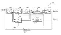
- FIG. 1illustrates a conventional self-biased phase-locked loop (PLL) integrated circuit 100 .
- This PLL integrated circuit 100includes: a phase-frequency detector 102 , first and second charge pumps 104 , 106 , a low pass filter 108 (containing a large capacitor 116 ), a bias generator 110 , a voltage-controlled oscillator 112 and a divide-by-N feedback circuit 114 , connected as illustrated.
- the inclusion of a pair of charge pumps 104 , 106supports a self-biasing configuration within the PLL integrated circuit 100 by allowing all bias currents and voltages to be referenced to other generated bias voltages and currents, which are established by the operating frequency.
- FIG. 1illustrates a conventional self-biased phase-locked loop (PLL) integrated circuit 100 .
- This PLL integrated circuit 100includes: a phase-frequency detector 102 , first and second charge pumps 104 , 106 , a low pass filter 108 (containing a large capacitor 116 ), a
- FIGS. 1 and 2are equivalent to FIGS. 1 and 5 of U.S. Pat. No. 5,727,037 to Maneatis. Additional PLL integrated circuits that utilize multiple charge pumps to support self-biased operation are disclosed in U.S. Pat. Nos. 6,329,882 and 6,894,569 to Fayneh et al.
- An integrated circuit chip that supports high speed serial/deserial (SERDES) operationsmay include many (e.g., >10) PLL integrated circuits that must run at target speeds (e.g., multi-GHZ frequencies) if the chip is to pass speed testing upon manufacture.
- the start and stop times of the reference time intervalmay be established by a reference counter that is responsive to a reference clock signal and the number of cycles of the divided clock signal may be measured by a target counter coupled to an output of the reference counter, which sets the start and stop time points.
- a reference counterthat is responsive to a reference clock signal
- the number of cycles of the divided clock signalmay be measured by a target counter coupled to an output of the reference counter, which sets the start and stop time points.
- speed testing of PLL integrated circuitsshould be performed as simply and as early in the chip manufacturing process as possible (e.g., at the wafer level) and should avoid the use of large test circuits (e.g., large counters).
- Embodiments of the present inventioninclude phase-locked and delay-locked loop integrated circuits that support efficient high speed testing of clock frequencies.
- an integrated circuit deviceis provided with a clock signal generator having at least one delay element therein that is responsive to a control signal.
- a speed tracking circuitis also provided. This speed tracking circuit is configured to generate a signal having a measurable characteristic that tracks changes in a property of the control signal that influences a delay of the at least one delay element.
- the measurable characteristicmay be a voltage of a signal and the property of the control signal may be its magnitude.
- the measurable characteristicmay be a frequency or phase of the signal, for example.
- Typical embodiments of the clock signal generatorinclude a self-biased phase-locked loop (PLL) integrated circuit and a self-biased delay-locked loop (DLL) integrated circuit.
- PLLphase-locked loop
- DLLdelay-locked loop
- a bias signal generator and a voltage-controlled oscillator (VCO)may be provided.
- the bias signal generatoris configured to generate a bias voltage in response to a control voltage and the voltage-controlled oscillator is responsive to the bias voltage.
- the bias signal generatormay be configured so that the bias voltage will track up and down changes in the control voltage.
- a speed tracking circuitis also provided. This speed tracking circuit is configured to support efficient speed testing by generating an output signal that tracks changes in a magnitude of the control voltage and also indirectly tracks changes in the bias voltage.
- the speed trackingcan be configured to generate an output voltage having a magnitude that is offset from the magnitude of the control voltage, which may be offset from a magnitude of the bias voltage.
- This output voltage generated by the speed tracking circuitmay be readily measured during wafer level yield testing to thereby improve testing efficiency and reduce manufacturing costs.
- a phase-locked loop (PLL) integrated circuitthat supports efficient high speed testing.
- This PLL integrated circuitincludes a bias signal generator configured to generate a bias voltage in response to at least one control voltage and a voltage-controlled oscillator configured to generate a clock signal in response to the bias voltage.
- a speed tracking circuitis also provided. The speed tracking circuit is configured to generate an output signal having a magnitude or other measurable characteristic (e.g, frequency, phase, etc.) that indicates whether or not a frequency of the clock signal is within a target range of acceptable frequencies.
- Additional embodiments of the inventioninclude delay-locked loop (DLL) integrated circuits.
- DLL integrated circuitsinclude a bias signal generator configured to generate a bias voltage in response to at least one control voltage and a voltage-controlled delay line configured to generate a clock signal in response to at least one bias voltage and a received clock signal (e.g., REFCLK).
- a speed tracking circuitis also provided. The speed tracking circuit is configured to generate an output signal having a measurable characteristic that indicates whether or not a frequency of the clock signal is within a target range of acceptable frequencies.
- FIG. 1is a block diagram of a conventional self-biased phase-locked loop (PLL) integrated circuit.
- PLLphase-locked loop
- FIG. 2is a block diagram of a conventional self-biased delay-locked loop (DLL) integrated circuit.
- DLLdelay-locked loop
- FIG. 3Ais a block diagram of a self-biased phase-locked loop (PLL) with control voltage tracking, according to embodiments of the present invention.
- PLLphase-locked loop
- FIG. 3Bis an electrical schematic of an embodiment of the bias signal generator illustrated by FIG. 3A .
- FIG. 3Cis an electrical schematic of an embodiment of the speed tracking circuit illustrated by FIG. 3A .
- FIG. 3Dis an electrical schematic of an embodiment of the voltage control oscillator illustrated by FIG. 3A .
- FIG. 4is a block diagram of a self-biased delay-locked loop (DLL) with control voltage tracking, according to embodiments of the present invention.
- DLLdelay-locked loop
- a self-biased phase-locked loop (PLL) 300includes: a phase-frequency detector (PFD) 302 , first and second charge pumps (CP 1 , CP 2 ) 304 , 306 , a low pass filter 308 , a bias signal generator 310 , a voltage-controlled oscillator (VCO) 312 , a divide-by-N feedback circuit 314 and a speed tracking circuit 316 , connected as illustrated.
- the phase-frequency detector 302is responsive to a reference clock signal REFCLK, which is provided to a first input terminal (VREF), and a feedback clock signal FBCLK, which is provided to a second input terminal (VIN).
- This feedback clock signal FBCLKis generated by a feedback circuit 314 , which is configured to divide a period of a generated clock signal (PLLCLK) by an integer amount.
- the PLL 300is configured to generate a high frequency output clock signal (PLLCLK) that is locked in phase to the reference clock signal REFCLK, which may have a lower frequency than the generated clock signal PLLCLK.
- the phase-frequency detector 302generates UP and DN control signals, which are provided as input signals to a pair of charge pumps 304 , 306 .
- the first and second charge pumps 304 , 306which are also responsive to a fed back control signal (shown as bias signal VBN), generate respective output signals ICP and IX (i.e., current signals), as illustrated.
- VBNfed back control signal
- ICP and IXi.e., current signals
- the output signal ICPis provided to the low pass filter 308 , which is shown in simplified form as a capacitor (C) having a relatively large capacitance value.
- the signal at the output of the low pass filter 308represents a control voltage (VCTRL) that is provided as an input to a first input terminal (IN 1 ) of the bias signal generator 310 .
- the output signal IXwhich is generated by the second charge pump 306 , is passed to a second input terminal (IN 2 ) of the bias signal generator 310 and as a bias input to the voltage-controlled oscillator 312 .
- the output signal IXmay also be passed through a filter, such as a ripple low pass filter containing a relatively small capacitor.
- FIG. 3Billustrates a bias signal generator 310 that is configured to generate a control signal (e.g., bias signal VBN) in response to the control voltage (VCTRL) provided to the first input terminal IN 1 and the output signal IX provided to the second input terminal IN 2 .
- the bias signal generator 310includes four PMOS transistors P 1 –P 4 , four NMOS transistors N 1 –N 4 and an operational amplifier (AMP), connected as illustrated.
- the NMOS transistors N 2 and N 4are biased to be normally-on transistors.
- the output of the operational amplifier AMPdrives gate terminals of NMOS transistors N 1 and N 3 .
- the operational amplifier AMPoperates to bias the NMOS transistor N 1 so that the “+” terminal of the AMP, which is commonly connected to drain terminals of the PMOS transistors P 1 and P 2 , tracks the voltage at the first input terminal IN 1 (i.e., the voltage at the “ ⁇ ” terminal of the AMP).
- the bias signal generator 310is also configured so that the drain-to-source current in the NMOS transistor N 2 is mirrored as the drain-to-source current in the NMOS transistor N 4 .
- the magnitude of the drain-to-source currentis also influenced by a magnitude of the voltage at the second input terminal IN 2 . As illustrated by FIG. 3A , this second input terminal IN 2 receives the output signal IX (a current signal) generated by the second charge pump 306 .
- the voltage-controlled oscillator 312is illustrated as including a plurality of differential amplifier stages DA 1 , DA 2 , . . . , DAn, which are electrically connected together in a ring oscillator configuration.
- the delay provided by each of these differential amplifier stages DA 1 , . . . , DAn,is controlled in a conventional manner by a magnitude of the signals VBN and VBP.
- the PLL 300may also be configured to drive the magnitude of the control voltage VCTRL and the bias signal VBN, which tracks changes in the control voltage, out of their respective acceptable ranges and saturate whenever phase locking between the reference clock signal REFCLK and the feedback clock signal FBCLK cannot be achieved.
- an acceptable range for the magnitude of the control voltage VCTRL during accurate phase-locked operationis between 450 mV and 750 mV
- an unacceptable value of the control voltage VCTRLwhich reflects in inability for the PLL 300 to achieve phase locking, may be below about 250 mV. This provides about a 200 mV offset (e.g., guard band) between the lowest acceptable control voltage and the highest unacceptable control voltage.
- Each differential output of each stage DA 1 , . . . , DAnis provided as an input to a clock buffer circuit 313 , which generates the output clock signal PLLCLK using conventional techniques.
- each differential output of each stage DA 1 , . . . , DAngenerates a distinct phase of the output clock signal PLLCLK.
- the clock buffer 313will receive eight clock signals that are separated in phase by multiples of 45° (i.e., 360°/8).
- the bias signal VBNmay be driven out of an acceptable range of voltages when the PLL 300 is unable to achieve a stable locking condition between the output clock signal PLLCLK and the reference clock signal REFCLK.
- the speed tracking circuit 316 of FIG. 3Cgenerates an output signal OUT (shown as VCTRL* in FIGS. 3A and 4 ) having a measurable characteristic (e.g., magnitude, frequency, phase, etc.) that identifies whether a magnitude of the bias signal VBN is within or without an acceptable range.
- This speed tracking circuit 316includes four PMOS transistors P 1 *–P 4 *, four NMOS transistors N 1 *–N 4 * and an operational amplifier (AMP*), connected as illustrated.
- the NMOS transistors N 2 * and N 4 *are biased to be normally-on transistors.
- the output of the operational amplifier AMP*drives gate terminals of NMOS transistors N 1 * and N 3 *.
- the vertical configuration of PMOS transistors P 3 * and P 4 * and NMOS transistors N 4 * and N 3 *supports the generation of an output signal OUT having a magnitude that is slightly offset relative to the voltage at the gate terminals of NMOS transistors N 1 * and N 2 *, which is itself slightly offset relative to the magnitude of the voltage at the input terminal IN (i.e., gate of PMOS transistor P 1 *).
- This input terminal INprovides no appreciable capacitive loading to the output of the low pass filter 308 , particularly when compared to the magnitude of the large capacitor C, and does not add appreciable noise to the control voltage. Accordingly, the output signal OUT (shown as VCTRL* in FIGS.
- control voltage VCTRL and bias voltage VBNcan be readily measured during wafer level testing to identify whether the control voltage VCTRL and bias voltage VBN are within respective acceptable ranges that indicate stable phase-locking of the PLL 300 .
- the actual value of the control voltage VCTRLmay also be used to classify parts within a range of acceptable performance levels.
- a self-biased delay-locked loop (DLL) 400includes: a phase-frequency detector (PFD) 402 , a charge pump (CP) 404 , a low pass filter 408 , a bias signal generator 410 , a voltage-controlled delay line (VCDL) 412 and a speed tracking circuit 416 , connected as illustrated.
- the voltage-controlled delay line 412may include a plurality of delay stages that are responsive to a pair of bias signals VBN and VBP that operate to set the delay provided by each stage.
- the phase-frequency detector 402is responsive to a reference clock signal REFCLK, which is provided to a first input terminal (VREF), and a feedback clock signal FBCLK, which is provided to a second input terminal (VIN).
- This feedback clock signalcorresponds to the output clock signal DLLCLK generated by the voltage-controlled delay line 412 .
- the DLL 400is configured to generate a high frequency output clock signal (DLLCLK) that is locked in phase to the reference clock signal REFCLK, which has an equivalent frequency. As described above with respect to FIG.
- the speed tracking circuit 416which may be equivalent to the speed tracking circuit 316 , generates an output voltage (shown as VCTRL*) that can be easily measured to identify whether the control voltage VCTRL and bias voltage VBN are within respective acceptable ranges that indicate stable phase-locking of the DLL 400 .
- VCTRL*an output voltage
Landscapes
- Stabilization Of Oscillater, Synchronisation, Frequency Synthesizers (AREA)
Abstract
Description
Claims (13)
Priority Applications (1)
| Application Number | Priority Date | Filing Date | Title |
|---|---|---|---|
| US11/264,111US7239188B1 (en) | 2005-11-01 | 2005-11-01 | Locked-loop integrated circuits having speed tracking circuits therein |
Applications Claiming Priority (1)
| Application Number | Priority Date | Filing Date | Title |
|---|---|---|---|
| US11/264,111US7239188B1 (en) | 2005-11-01 | 2005-11-01 | Locked-loop integrated circuits having speed tracking circuits therein |
Publications (1)
| Publication Number | Publication Date |
|---|---|
| US7239188B1true US7239188B1 (en) | 2007-07-03 |
Family
ID=38196809
Family Applications (1)
| Application Number | Title | Priority Date | Filing Date |
|---|---|---|---|
| US11/264,111Active2025-11-11US7239188B1 (en) | 2005-11-01 | 2005-11-01 | Locked-loop integrated circuits having speed tracking circuits therein |
Country Status (1)
| Country | Link |
|---|---|
| US (1) | US7239188B1 (en) |
Cited By (36)
| Publication number | Priority date | Publication date | Assignee | Title |
|---|---|---|---|---|
| US20070035337A1 (en)* | 2005-08-10 | 2007-02-15 | Samsung Electronics Co., Ltd. | Lock detector and delay-locked loop having the same |
| US20080129388A1 (en)* | 2006-11-30 | 2008-06-05 | Motorola, Inc. | System and method for reducing transient responses in a phase lock loop with variable oscillator gain |
| US20080186781A1 (en)* | 2006-09-29 | 2008-08-07 | Hynix Semiconductor Inc. | Semiconductor memory device |
| US20090189658A1 (en)* | 2008-01-25 | 2009-07-30 | Elpida Memory, Inc. | DLL circuit, semiconductor device using the same, and method for controlling DLL circuit |
| US7586347B1 (en)* | 2007-09-27 | 2009-09-08 | Integrated Device Technology, Inc. | Clock generator with self-bias bandwidth control |
| US20100102862A1 (en)* | 2008-10-23 | 2010-04-29 | Elpida Memory, Inc. | Dll circuit and control method therefor |
| US20100277356A1 (en)* | 2008-01-09 | 2010-11-04 | Takashi Michiyochi | Oscillation frequency control circuit, dc-dc converter including the oscillation frequency control circuit, and semiconductor device |
| US20110098977A1 (en)* | 2009-10-28 | 2011-04-28 | Integrated Device Technology, Inc. | High speed chip screening method using delay locked loop |
| US20130120040A1 (en)* | 2011-11-10 | 2013-05-16 | Qualcomm Incorporated | System and method of stabilizing charge pump node voltage levels |
| US20130154697A1 (en)* | 2011-12-15 | 2013-06-20 | Renesas Electronics Corporation | Pll circuit |
| US20140354341A1 (en)* | 2013-05-31 | 2014-12-04 | Broadcom Corporation | Chip instrumentation for in-situ clock domain characterization |
| US9197263B2 (en) | 2011-07-26 | 2015-11-24 | Sumitomo Electric Industries, Ltd. | Compensation apparatus, signal generator and wireless communication equipment |
| US20160173080A1 (en)* | 2012-05-29 | 2016-06-16 | Life Technologies Corporation | System for reducing noise in a chemical sensor array |
| US9455823B2 (en)* | 2015-02-24 | 2016-09-27 | Pixart Imaging Inc. | Four-phase clock generator with timing sequence self-detection |
| US9841398B2 (en) | 2013-01-08 | 2017-12-12 | Life Technologies Corporation | Methods for manufacturing well structures for low-noise chemical sensors |
| US9927393B2 (en) | 2009-05-29 | 2018-03-27 | Life Technologies Corporation | Methods and apparatus for measuring analytes |
| US9944981B2 (en) | 2008-10-22 | 2018-04-17 | Life Technologies Corporation | Methods and apparatus for measuring analytes |
| US9951382B2 (en) | 2006-12-14 | 2018-04-24 | Life Technologies Corporation | Methods and apparatus for measuring analytes using large scale FET arrays |
| US9958414B2 (en) | 2010-09-15 | 2018-05-01 | Life Technologies Corporation | Apparatus for measuring analytes including chemical sensor array |
| US9960253B2 (en) | 2010-07-03 | 2018-05-01 | Life Technologies Corporation | Chemically sensitive sensor with lightly doped drains |
| US9964977B2 (en)* | 2015-10-30 | 2018-05-08 | Taiwan Semiconductor Manufacturing Co., Ltd. | Device and method for body-bias |
| US9970984B2 (en) | 2011-12-01 | 2018-05-15 | Life Technologies Corporation | Method and apparatus for identifying defects in a chemical sensor array |
| US9989489B2 (en) | 2006-12-14 | 2018-06-05 | Life Technnologies Corporation | Methods for calibrating an array of chemically-sensitive sensors |
| US9995708B2 (en) | 2013-03-13 | 2018-06-12 | Life Technologies Corporation | Chemical sensor with sidewall spacer sensor surface |
| US10077472B2 (en) | 2014-12-18 | 2018-09-18 | Life Technologies Corporation | High data rate integrated circuit with power management |
| US10422767B2 (en) | 2013-03-15 | 2019-09-24 | Life Technologies Corporation | Chemical sensor with consistent sensor surface areas |
| US10458942B2 (en) | 2013-06-10 | 2019-10-29 | Life Technologies Corporation | Chemical sensor array having multiple sensors per well |
| US10481123B2 (en) | 2010-06-30 | 2019-11-19 | Life Technologies Corporation | Ion-sensing charge-accumulation circuits and methods |
| US10523221B2 (en)* | 2016-11-30 | 2019-12-31 | Taiwan Semiconductor Manufacturing Co., Ltd. | Hybrid phase lock loop |
| US10605767B2 (en) | 2014-12-18 | 2020-03-31 | Life Technologies Corporation | High data rate integrated circuit with transmitter configuration |
| US10641729B2 (en) | 2010-06-30 | 2020-05-05 | Life Technologies Corporation | Column ADC |
| US10718733B2 (en) | 2009-05-29 | 2020-07-21 | Life Technologies Corporation | Methods and apparatus for measuring analytes |
| US11231451B2 (en) | 2010-06-30 | 2022-01-25 | Life Technologies Corporation | Methods and apparatus for testing ISFET arrays |
| US11307166B2 (en) | 2010-07-01 | 2022-04-19 | Life Technologies Corporation | Column ADC |
| US20230081578A1 (en)* | 2021-09-10 | 2023-03-16 | Maxim Integrated Products, Inc. | Transmitting clock reference over reverse channel in a bidirectional serial link |
| US20230387919A1 (en)* | 2022-05-24 | 2023-11-30 | Airoha Technology Corp. | Biasing circuit for setting bias volatges of current source circuit and current sink circuit in charge pump of phase-locked loop circuit by using current digital-to-analog converter and low-pass filter |
Citations (21)
| Publication number | Priority date | Publication date | Assignee | Title |
|---|---|---|---|---|
| US5629650A (en) | 1996-01-29 | 1997-05-13 | International Business Machines Corporation | Self-biased phase-locked loop |
| US5686864A (en)* | 1995-09-05 | 1997-11-11 | Motorola, Inc. | Method and apparatus for controlling a voltage controlled oscillator tuning range in a frequency synthesizer |
| US5727037A (en) | 1996-01-26 | 1998-03-10 | Silicon Graphics, Inc. | System and method to reduce phase offset and phase jitter in phase-locked and delay-locked loops using self-biased circuits |
| US5942949A (en)* | 1997-10-14 | 1999-08-24 | Lucent Technologies Inc. | Self-calibrating phase-lock loop with auto-trim operations for selecting an appropriate oscillator operating curve |
| US5982836A (en)* | 1994-11-04 | 1999-11-09 | Fujitsu Limited | Phase synchronizer and data reproducing apparatus |
| US6031427A (en)* | 1997-03-06 | 2000-02-29 | Texas Instruments Incorporated | System for sweeping a phase lock loop into lock with automatic initiation and shutdown |
| US6043695A (en)* | 1997-05-29 | 2000-03-28 | Nec Corporation | Phase locked loop using a schmitt trigger block |
| US6275115B1 (en)* | 1999-03-01 | 2001-08-14 | Kabushiki Kaisha Toshiba | PLL circuit having current control oscillator receiving the sum of two control currents |
| US6329882B1 (en) | 1999-12-20 | 2001-12-11 | Intel Corporation | Third-order self-biased phase-locked loop for low jitter applications |
| US6411144B1 (en)* | 1999-08-05 | 2002-06-25 | Fujitsu Quantum Devices Limited | Phase-locked loop circuit |
| US6661267B2 (en)* | 2002-05-06 | 2003-12-09 | International Business Machines Corporation | Coarse calibration circuit using variable step sizes to reduce jitter and a dynamic course calibration (DCC) circuit for a 2 GHz VCO |
| US6744293B1 (en)* | 2002-04-09 | 2004-06-01 | Applied Micro Circuits Corporation | Global clock tree de-skew |
| US6784707B2 (en)* | 2002-07-10 | 2004-08-31 | The Board Of Trustees Of The University Of Illinois | Delay locked loop clock generator |
| US6867627B1 (en) | 2003-09-16 | 2005-03-15 | Integrated Device Technology, Inc. | Delay-locked loop (DLL) integrated circuits having high bandwidth and reliable locking characteristics |
| US6894569B2 (en) | 2002-12-30 | 2005-05-17 | Intel Corporation | High-performance charge pump for self-biased phase-locked loop |
| US6903586B2 (en) | 2003-02-28 | 2005-06-07 | Ati Technologies, Inc. | Gain control circuitry for delay locked loop circuit |
| US6952124B2 (en)* | 2003-09-15 | 2005-10-04 | Silicon Bridge, Inc. | Phase locked loop circuit with self adjusted tuning hiep the pham |
| US6963234B2 (en)* | 2000-11-21 | 2005-11-08 | Micronas Gmbh | Phase regulating circuit with a time-delay element |
| US6987409B2 (en)* | 2003-01-09 | 2006-01-17 | Hynix Semiconductor Inc. | Analog delay locked loop with tracking analog-digital converter |
| US7061332B2 (en)* | 2004-09-30 | 2006-06-13 | Texas Instruments Incorporated | Process tracking limiter for VCO control voltages |
| US7109764B2 (en)* | 2003-11-10 | 2006-09-19 | Sharp Kabushiki Kaisha | PLL clock signal generation circuit |
- 2005
- 2005-11-01USUS11/264,111patent/US7239188B1/enactiveActive
Patent Citations (21)
| Publication number | Priority date | Publication date | Assignee | Title |
|---|---|---|---|---|
| US5982836A (en)* | 1994-11-04 | 1999-11-09 | Fujitsu Limited | Phase synchronizer and data reproducing apparatus |
| US5686864A (en)* | 1995-09-05 | 1997-11-11 | Motorola, Inc. | Method and apparatus for controlling a voltage controlled oscillator tuning range in a frequency synthesizer |
| US5727037A (en) | 1996-01-26 | 1998-03-10 | Silicon Graphics, Inc. | System and method to reduce phase offset and phase jitter in phase-locked and delay-locked loops using self-biased circuits |
| US5629650A (en) | 1996-01-29 | 1997-05-13 | International Business Machines Corporation | Self-biased phase-locked loop |
| US6031427A (en)* | 1997-03-06 | 2000-02-29 | Texas Instruments Incorporated | System for sweeping a phase lock loop into lock with automatic initiation and shutdown |
| US6043695A (en)* | 1997-05-29 | 2000-03-28 | Nec Corporation | Phase locked loop using a schmitt trigger block |
| US5942949A (en)* | 1997-10-14 | 1999-08-24 | Lucent Technologies Inc. | Self-calibrating phase-lock loop with auto-trim operations for selecting an appropriate oscillator operating curve |
| US6275115B1 (en)* | 1999-03-01 | 2001-08-14 | Kabushiki Kaisha Toshiba | PLL circuit having current control oscillator receiving the sum of two control currents |
| US6411144B1 (en)* | 1999-08-05 | 2002-06-25 | Fujitsu Quantum Devices Limited | Phase-locked loop circuit |
| US6329882B1 (en) | 1999-12-20 | 2001-12-11 | Intel Corporation | Third-order self-biased phase-locked loop for low jitter applications |
| US6963234B2 (en)* | 2000-11-21 | 2005-11-08 | Micronas Gmbh | Phase regulating circuit with a time-delay element |
| US6744293B1 (en)* | 2002-04-09 | 2004-06-01 | Applied Micro Circuits Corporation | Global clock tree de-skew |
| US6661267B2 (en)* | 2002-05-06 | 2003-12-09 | International Business Machines Corporation | Coarse calibration circuit using variable step sizes to reduce jitter and a dynamic course calibration (DCC) circuit for a 2 GHz VCO |
| US6784707B2 (en)* | 2002-07-10 | 2004-08-31 | The Board Of Trustees Of The University Of Illinois | Delay locked loop clock generator |
| US6894569B2 (en) | 2002-12-30 | 2005-05-17 | Intel Corporation | High-performance charge pump for self-biased phase-locked loop |
| US6987409B2 (en)* | 2003-01-09 | 2006-01-17 | Hynix Semiconductor Inc. | Analog delay locked loop with tracking analog-digital converter |
| US6903586B2 (en) | 2003-02-28 | 2005-06-07 | Ati Technologies, Inc. | Gain control circuitry for delay locked loop circuit |
| US6952124B2 (en)* | 2003-09-15 | 2005-10-04 | Silicon Bridge, Inc. | Phase locked loop circuit with self adjusted tuning hiep the pham |
| US6867627B1 (en) | 2003-09-16 | 2005-03-15 | Integrated Device Technology, Inc. | Delay-locked loop (DLL) integrated circuits having high bandwidth and reliable locking characteristics |
| US7109764B2 (en)* | 2003-11-10 | 2006-09-19 | Sharp Kabushiki Kaisha | PLL clock signal generation circuit |
| US7061332B2 (en)* | 2004-09-30 | 2006-06-13 | Texas Instruments Incorporated | Process tracking limiter for VCO control voltages |
Non-Patent Citations (5)
| Title |
|---|
| Maneatis, John G., "FA8.1 Low-Jitter and Process-Independent DLL and PLL Based on Self-Biased Techniques," IEEE International Solid-State Circuits Conference, Digest of Technical Papers, pp. 130-132, no date. |
| Maneatis, John G., "Low-Jitter Process-Independent DLL and PLL Based on Self-Biased Techniques," IEEE Journal of Solid-State Circuits, vol. 31, No. 11, Nov. 1996. |
| Maneatis, John G., Low-Jitter Process-Independent DLL and PLL Based on Self-Biased Techniques, High Speed CMOS IC Lab, Postech, Dec. 24, 2004, http://aslc.postech.ac.kr/3.Class/1.Classes/04<SUB>-</SUB>695v/1224bjh.pdf. |
| Mansuri et al., "A Low-Power Adaptive Bandwidth PLL and Clock Buffer with Supply-Noise Compensation," IEEE Journal of Solid-State Circuits, vol. 38, No. 11, Nov. 2003. |
| Sidiropoulos, et al., "SA 20.2: A Semi-Digital DLL with Unlimited Phase Shift Capability and 0.08-400MHz Operating Range," Center for Integrated Systems, Stanford University, Stanford, CA, Admitted Prior Art, no date. |
Cited By (77)
| Publication number | Priority date | Publication date | Assignee | Title |
|---|---|---|---|---|
| US20070035337A1 (en)* | 2005-08-10 | 2007-02-15 | Samsung Electronics Co., Ltd. | Lock detector and delay-locked loop having the same |
| US7508245B2 (en)* | 2005-08-10 | 2009-03-24 | Samsung Electronics Co., Ltd. | Lock detector and delay-locked loop having the same |
| US20080186781A1 (en)* | 2006-09-29 | 2008-08-07 | Hynix Semiconductor Inc. | Semiconductor memory device |
| US7495486B2 (en)* | 2006-09-29 | 2009-02-24 | Hynix Semiconductor Inc. | Semiconductor memory device |
| US20080129388A1 (en)* | 2006-11-30 | 2008-06-05 | Motorola, Inc. | System and method for reducing transient responses in a phase lock loop with variable oscillator gain |
| US9989489B2 (en) | 2006-12-14 | 2018-06-05 | Life Technnologies Corporation | Methods for calibrating an array of chemically-sensitive sensors |
| US9951382B2 (en) | 2006-12-14 | 2018-04-24 | Life Technologies Corporation | Methods and apparatus for measuring analytes using large scale FET arrays |
| US10203300B2 (en) | 2006-12-14 | 2019-02-12 | Life Technologies Corporation | Methods and apparatus for measuring analytes using large scale FET arrays |
| US7586347B1 (en)* | 2007-09-27 | 2009-09-08 | Integrated Device Technology, Inc. | Clock generator with self-bias bandwidth control |
| US20100277356A1 (en)* | 2008-01-09 | 2010-11-04 | Takashi Michiyochi | Oscillation frequency control circuit, dc-dc converter including the oscillation frequency control circuit, and semiconductor device |
| KR101156910B1 (en) | 2008-01-09 | 2012-06-21 | 가부시키가이샤 리코 | Oscillation frequency control circuit, dc-dc converter including the oscillation frequency control circuit, and semiconductor device |
| US8212598B2 (en)* | 2008-01-09 | 2012-07-03 | Ricoh Company, Ltd. | Oscillation frequency control circuit, DC-DC converter including the oscillation frequency control circuit, and semiconductor device |
| US7724051B2 (en)* | 2008-01-25 | 2010-05-25 | Elpida Memory, Inc. | DLL circuit, semiconductor device using the same, and method for controlling DLL circuit |
| US20090189658A1 (en)* | 2008-01-25 | 2009-07-30 | Elpida Memory, Inc. | DLL circuit, semiconductor device using the same, and method for controlling DLL circuit |
| US11137369B2 (en) | 2008-10-22 | 2021-10-05 | Life Technologies Corporation | Integrated sensor arrays for biological and chemical analysis |
| US12146853B2 (en) | 2008-10-22 | 2024-11-19 | Life Technologies Corporation | Methods and apparatus including array of reaction chambers over array of chemFET sensors for measuring analytes |
| US9964515B2 (en) | 2008-10-22 | 2018-05-08 | Life Technologies Corporation | Integrated sensor arrays for biological and chemical analysis |
| US9944981B2 (en) | 2008-10-22 | 2018-04-17 | Life Technologies Corporation | Methods and apparatus for measuring analytes |
| US11448613B2 (en) | 2008-10-22 | 2022-09-20 | Life Technologies Corporation | ChemFET sensor array including overlying array of wells |
| US11874250B2 (en) | 2008-10-22 | 2024-01-16 | Life Technologies Corporation | Integrated sensor arrays for biological and chemical analysis |
| US8063679B2 (en)* | 2008-10-23 | 2011-11-22 | Elpida Memory, Inc. | DLL circuit and control method therefor |
| US20100102862A1 (en)* | 2008-10-23 | 2010-04-29 | Elpida Memory, Inc. | Dll circuit and control method therefor |
| US12038405B2 (en) | 2009-05-29 | 2024-07-16 | Life Technologies Corporation | Methods and apparatus for measuring analytes |
| US10718733B2 (en) | 2009-05-29 | 2020-07-21 | Life Technologies Corporation | Methods and apparatus for measuring analytes |
| US11768171B2 (en) | 2009-05-29 | 2023-09-26 | Life Technologies Corporation | Methods and apparatus for measuring analytes |
| US11692964B2 (en) | 2009-05-29 | 2023-07-04 | Life Technologies Corporation | Methods and apparatus for measuring analytes |
| US9927393B2 (en) | 2009-05-29 | 2018-03-27 | Life Technologies Corporation | Methods and apparatus for measuring analytes |
| US10809226B2 (en) | 2009-05-29 | 2020-10-20 | Life Technologies Corporation | Methods and apparatus for measuring analytes |
| US8548773B2 (en)* | 2009-10-28 | 2013-10-01 | Integrated Device Technology, Inc. | High speed chip screening method using delay locked loop |
| US20110098977A1 (en)* | 2009-10-28 | 2011-04-28 | Integrated Device Technology, Inc. | High speed chip screening method using delay locked loop |
| US12038406B2 (en) | 2010-06-30 | 2024-07-16 | Life Technologies Corporation | Semiconductor-based chemical detection device |
| US10641729B2 (en) | 2010-06-30 | 2020-05-05 | Life Technologies Corporation | Column ADC |
| US11231451B2 (en) | 2010-06-30 | 2022-01-25 | Life Technologies Corporation | Methods and apparatus for testing ISFET arrays |
| US10481123B2 (en) | 2010-06-30 | 2019-11-19 | Life Technologies Corporation | Ion-sensing charge-accumulation circuits and methods |
| US11307166B2 (en) | 2010-07-01 | 2022-04-19 | Life Technologies Corporation | Column ADC |
| US9960253B2 (en) | 2010-07-03 | 2018-05-01 | Life Technologies Corporation | Chemically sensitive sensor with lightly doped drains |
| US12050195B2 (en) | 2010-09-15 | 2024-07-30 | Life Technologies Corporation | Methods and apparatus for measuring analytes using chemfet arrays |
| US9958415B2 (en) | 2010-09-15 | 2018-05-01 | Life Technologies Corporation | ChemFET sensor including floating gate |
| US9958414B2 (en) | 2010-09-15 | 2018-05-01 | Life Technologies Corporation | Apparatus for measuring analytes including chemical sensor array |
| US9281989B2 (en)* | 2011-07-26 | 2016-03-08 | Sumitomo Electric Industries, Ltd. | Compensation apparatus, signal generator and wireless communication equipment |
| US9197263B2 (en) | 2011-07-26 | 2015-11-24 | Sumitomo Electric Industries, Ltd. | Compensation apparatus, signal generator and wireless communication equipment |
| US20130120040A1 (en)* | 2011-11-10 | 2013-05-16 | Qualcomm Incorporated | System and method of stabilizing charge pump node voltage levels |
| US8581647B2 (en)* | 2011-11-10 | 2013-11-12 | Qualcomm Incorporated | System and method of stabilizing charge pump node voltage levels |
| US9970984B2 (en) | 2011-12-01 | 2018-05-15 | Life Technologies Corporation | Method and apparatus for identifying defects in a chemical sensor array |
| US10365321B2 (en) | 2011-12-01 | 2019-07-30 | Life Technologies Corporation | Method and apparatus for identifying defects in a chemical sensor array |
| US10598723B2 (en) | 2011-12-01 | 2020-03-24 | Life Technologies Corporation | Method and apparatus for identifying defects in a chemical sensor array |
| US20140320185A1 (en)* | 2011-12-15 | 2014-10-30 | Renesas Electronics Corporation | Pll circuit |
| US20130154697A1 (en)* | 2011-12-15 | 2013-06-20 | Renesas Electronics Corporation | Pll circuit |
| US8810292B2 (en)* | 2011-12-15 | 2014-08-19 | Renesas Electronics Corporation | PLL circuit |
| US8981825B2 (en)* | 2011-12-15 | 2015-03-17 | Renesas Electronics Corporation | PLL circuit |
| US10404249B2 (en) | 2012-05-29 | 2019-09-03 | Life Technologies Corporation | System for reducing noise in a chemical sensor array |
| US20160173080A1 (en)* | 2012-05-29 | 2016-06-16 | Life Technologies Corporation | System for reducing noise in a chemical sensor array |
| US9985624B2 (en)* | 2012-05-29 | 2018-05-29 | Life Technologies Corporation | System for reducing noise in a chemical sensor array |
| US9841398B2 (en) | 2013-01-08 | 2017-12-12 | Life Technologies Corporation | Methods for manufacturing well structures for low-noise chemical sensors |
| US10436742B2 (en) | 2013-01-08 | 2019-10-08 | Life Technologies Corporation | Methods for manufacturing well structures for low-noise chemical sensors |
| US9995708B2 (en) | 2013-03-13 | 2018-06-12 | Life Technologies Corporation | Chemical sensor with sidewall spacer sensor surface |
| US10422767B2 (en) | 2013-03-15 | 2019-09-24 | Life Technologies Corporation | Chemical sensor with consistent sensor surface areas |
| US20140354341A1 (en)* | 2013-05-31 | 2014-12-04 | Broadcom Corporation | Chip instrumentation for in-situ clock domain characterization |
| US9075104B2 (en)* | 2013-05-31 | 2015-07-07 | Broadcom Corporation | Chip instrumentation for in-situ clock domain characterization |
| US11499938B2 (en) | 2013-06-10 | 2022-11-15 | Life Technologies Corporation | Chemical sensor array having multiple sensors per well |
| US10816504B2 (en) | 2013-06-10 | 2020-10-27 | Life Technologies Corporation | Chemical sensor array having multiple sensors per well |
| US10458942B2 (en) | 2013-06-10 | 2019-10-29 | Life Technologies Corporation | Chemical sensor array having multiple sensors per well |
| US11774401B2 (en) | 2013-06-10 | 2023-10-03 | Life Technologies Corporation | Chemical sensor array having multiple sensors per well |
| US10605767B2 (en) | 2014-12-18 | 2020-03-31 | Life Technologies Corporation | High data rate integrated circuit with transmitter configuration |
| US10767224B2 (en) | 2014-12-18 | 2020-09-08 | Life Technologies Corporation | High data rate integrated circuit with power management |
| US12196704B2 (en) | 2014-12-18 | 2025-01-14 | Life Technologies Corporation | High data rate integrated circuit with transmitter configuration |
| US11536688B2 (en) | 2014-12-18 | 2022-12-27 | Life Technologies Corporation | High data rate integrated circuit with transmitter configuration |
| US10077472B2 (en) | 2014-12-18 | 2018-09-18 | Life Technologies Corporation | High data rate integrated circuit with power management |
| US9455823B2 (en)* | 2015-02-24 | 2016-09-27 | Pixart Imaging Inc. | Four-phase clock generator with timing sequence self-detection |
| US9964977B2 (en)* | 2015-10-30 | 2018-05-08 | Taiwan Semiconductor Manufacturing Co., Ltd. | Device and method for body-bias |
| US10523221B2 (en)* | 2016-11-30 | 2019-12-31 | Taiwan Semiconductor Manufacturing Co., Ltd. | Hybrid phase lock loop |
| US10749537B2 (en)* | 2016-11-30 | 2020-08-18 | Taiwan Semiconductor Manufacturing Co., Ltd. | Hybrid phase lock loop |
| US12003612B2 (en)* | 2021-09-10 | 2024-06-04 | Maxim Integrated Products, Inc. | Transmitting clock reference over reverse channel in a bidirectional serial link |
| US20230081578A1 (en)* | 2021-09-10 | 2023-03-16 | Maxim Integrated Products, Inc. | Transmitting clock reference over reverse channel in a bidirectional serial link |
| US12316729B2 (en) | 2021-09-10 | 2025-05-27 | Maxim Integrated Products, Inc. | Transmitting clock reference over reverse channel in a bidirectional serial link |
| US20230387919A1 (en)* | 2022-05-24 | 2023-11-30 | Airoha Technology Corp. | Biasing circuit for setting bias volatges of current source circuit and current sink circuit in charge pump of phase-locked loop circuit by using current digital-to-analog converter and low-pass filter |
| US12255659B2 (en)* | 2022-05-24 | 2025-03-18 | Airoha Technology Corp. | Biasing circuit for setting bias voltages of current source circuit and current sink circuit in charge pump of phase-locked loop circuit by using current digital-to-analog converter and low-pass filter |
Similar Documents
| Publication | Publication Date | Title |
|---|---|---|
| US7239188B1 (en) | Locked-loop integrated circuits having speed tracking circuits therein | |
| Foley et al. | CMOS DLL-based 2-V 3.2-ps jitter 1-GHz clock synthesizer and temperature-compensated tunable oscillator | |
| Moon et al. | An all-analog multiphase delay-locked loop using a replica delay line for wide-range operation and low-jitter performance | |
| US7855933B2 (en) | Clock synchronization circuit and operation method thereof | |
| US6867627B1 (en) | Delay-locked loop (DLL) integrated circuits having high bandwidth and reliable locking characteristics | |
| US6608511B1 (en) | Charge-pump phase-locked loop circuit with charge calibration | |
| US8232822B2 (en) | Charge pump and phase-detecting apparatus, phase-locked loop and delay-locked loop using the same | |
| US6329882B1 (en) | Third-order self-biased phase-locked loop for low jitter applications | |
| US20070109030A1 (en) | Phase-Locked Loop Integrated Circuits Having Fast Phase Locking Characteristics | |
| US20040008063A1 (en) | Delay locked loop clock generator | |
| US10476511B2 (en) | PLL circuit, semiconductor device including the same, and control method of PLL circuit | |
| US7538591B2 (en) | Fast locking phase locked loop for synchronization with an input signal | |
| US7154352B2 (en) | Clock generator and related biasing circuit | |
| US6927635B2 (en) | Lock detectors having a narrow sensitivity range | |
| US8786315B2 (en) | Phase frequency detector | |
| CN115765728B (en) | Phase frequency detector and phase-locked loop | |
| US6717446B1 (en) | High speed programmable charge-pump with low charge injection | |
| TWI416877B (en) | Charge pumper and phase-detecting apparatus, phase-locked loop and delay-locked loop using the same | |
| US6778026B2 (en) | High-speed phase frequency detection module | |
| JP2012034212A (en) | Phase-locked loop circuit | |
| KR101480621B1 (en) | Clock Generator of using Delay-Locked Loop | |
| US7659785B2 (en) | Voltage controlled oscillator and PLL having the same | |
| US9553718B2 (en) | PLL circuit and control method thereof | |
| US7162001B2 (en) | Charge pump with transient current correction | |
| JP5799828B2 (en) | Phase lock loop circuit |
Legal Events
| Date | Code | Title | Description |
|---|---|---|---|
| AS | Assignment | Owner name:INTEGRATED DEVICE TECHNOLOGY, INC., CALIFORNIA Free format text:ASSIGNMENT OF ASSIGNORS INTEREST;ASSIGNORS:XU, CHAO;FANG, AL XUEFENG;REEL/FRAME:017169/0075 Effective date:20051101 | |
| FEPP | Fee payment procedure | Free format text:PAYOR NUMBER ASSIGNED (ORIGINAL EVENT CODE: ASPN); ENTITY STATUS OF PATENT OWNER: LARGE ENTITY | |
| STCF | Information on status: patent grant | Free format text:PATENTED CASE | |
| FPAY | Fee payment | Year of fee payment:4 | |
| FPAY | Fee payment | Year of fee payment:8 | |
| AS | Assignment | Owner name:JPMORGAN CHASE BANK, N.A., AS COLLATERAL AGENT, NE Free format text:SECURITY AGREEMENT;ASSIGNORS:INTEGRATED DEVICE TECHNOLOGY, INC.;GIGPEAK, INC.;MAGNUM SEMICONDUCTOR, INC.;AND OTHERS;REEL/FRAME:042166/0431 Effective date:20170404 Owner name:JPMORGAN CHASE BANK, N.A., AS COLLATERAL AGENT, NEW YORK Free format text:SECURITY AGREEMENT;ASSIGNORS:INTEGRATED DEVICE TECHNOLOGY, INC.;GIGPEAK, INC.;MAGNUM SEMICONDUCTOR, INC.;AND OTHERS;REEL/FRAME:042166/0431 Effective date:20170404 | |
| MAFP | Maintenance fee payment | Free format text:PAYMENT OF MAINTENANCE FEE, 12TH YEAR, LARGE ENTITY (ORIGINAL EVENT CODE: M1553); ENTITY STATUS OF PATENT OWNER: LARGE ENTITY Year of fee payment:12 | |
| AS | Assignment | Owner name:INTEGRATED DEVICE TECHNOLOGY, INC., CALIFORNIA Free format text:RELEASE BY SECURED PARTY;ASSIGNOR:JPMORGAN CHASE BANK, N.A.;REEL/FRAME:048746/0001 Effective date:20190329 Owner name:CHIPX, INCORPORATED, CALIFORNIA Free format text:RELEASE BY SECURED PARTY;ASSIGNOR:JPMORGAN CHASE BANK, N.A.;REEL/FRAME:048746/0001 Effective date:20190329 Owner name:MAGNUM SEMICONDUCTOR, INC., CALIFORNIA Free format text:RELEASE BY SECURED PARTY;ASSIGNOR:JPMORGAN CHASE BANK, N.A.;REEL/FRAME:048746/0001 Effective date:20190329 Owner name:GIGPEAK, INC., CALIFORNIA Free format text:RELEASE BY SECURED PARTY;ASSIGNOR:JPMORGAN CHASE BANK, N.A.;REEL/FRAME:048746/0001 Effective date:20190329 Owner name:ENDWAVE CORPORATION, CALIFORNIA Free format text:RELEASE BY SECURED PARTY;ASSIGNOR:JPMORGAN CHASE BANK, N.A.;REEL/FRAME:048746/0001 Effective date:20190329 |