US7236757B2 - High-speed multi-channel communications transceiver with inter-channel interference filter - Google Patents
High-speed multi-channel communications transceiver with inter-channel interference filterDownload PDFInfo
- Publication number
- US7236757B2 US7236757B2US10/071,771US7177102AUS7236757B2US 7236757 B2US7236757 B2US 7236757B2US 7177102 AUS7177102 AUS 7177102AUS 7236757 B2US7236757 B2US 7236757B2
- Authority
- US
- United States
- Prior art keywords
- signal
- signals
- phase
- quadrature
- data
- Prior art date
- Legal status (The legal status is an assumption and is not a legal conclusion. Google has not performed a legal analysis and makes no representation as to the accuracy of the status listed.)
- Expired - Lifetime, expires
Links
Images


Classifications
- H—ELECTRICITY
- H04—ELECTRIC COMMUNICATION TECHNIQUE
- H04L—TRANSMISSION OF DIGITAL INFORMATION, e.g. TELEGRAPHIC COMMUNICATION
- H04L27/00—Modulated-carrier systems
- H04L27/26—Systems using multi-frequency codes
- H04L27/2601—Multicarrier modulation systems
Definitions
- the present inventionis related to high-speed communications of data in a communication system and, in particular, to high data rate transmission of data between components in a communication system.
- NRZnon-return to zero
- SERDESserializer/deserializer
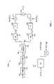
- FIG. 1Ashows a block diagram of a backplane environment 100 .
- Components 101 - 1 through 101 -Qare coupled to transmit and receive data through input/output (I/O) ports 102 - 1 through 102 -Q, respectively, to backplane 110 .
- I/Oinput/output
- components 101 - 1 through 101 -Qare SERDES devices.
- FIG. 1Bshows a block diagram of a conventional transmitter portion of one of SERDES devices 101 - 1 through 101 -Q on I/O ports 102 - 1 through 102 -Q, respectively.
- Parallel datais received in a bit encoder 105 .
- Bit encoder 105encodes the parallel data, for example by adding redundancy in the input data, to ensure a minimum rate of data transitions in the output data stream. Typical encoding schemes include rate 8/10 (8 bit input to 10 bit output) encoding.
- the parallel datais serialized in parallel to serial converter 106 .
- Output driver 107then receives the serialized data from parallel to serial converter 106 and outputs, usually, a differential voltage signal for transmission over backplane 110 .
- phase locked loop (PLL) 114that provides the necessary clock signals for encoder 105 and parallel-to-serial converter 106 .
- the input signal to PLL 114is a reference clock signal from a system PLL 103 .
- FIG. 1Cshows a conventional receiver 108 of one of SERDES devices 101 - 1 through 101 -Q on I/O ports 102 - 1 through 102 -Q, respectively, of FIG. 1A .
- Input driver 109receives differential voltage signal from backplane 110 and outputs the analog data signal to clock and data recovery circuit 113 .
- Data recovery 113can, in some systems, perform equalization, recover the timing and output a serial bit stream of data to serial-to-parallel converter 111 .
- the serial datais input to bit decoder 112 which converts the parallel data to parallel decoded data.
- Clock and data recovery circuit 113also outputs the necessary clock signals to serial-to-parallel converter 111 and bit decoder 112 .
- a conventional SERDES system 100can enable serial data communication at data rates as high as 2.5 Gbps to 3.125 Gbps over a pair of FR4 copper traces in a copper backplane communication system.
- One of the biggest problems with existing SERDES systems 100is that they are very bandwidth inefficient, i.e., they require 3.125 GHz of bandwidth to transmit and receive 2.5 Gbps of data over a single pair of copper wires. Therefore, it is very difficult to increase the data rates across backplane bus 110 .
- SERDES system 100requires the implementation of a high clock rate (3.125 GHz for 2.5 Gbps data rates) phase locked loop (PLL) 114 implemented to transmit data and recover high clock rates in data recovery 113 .
- PLLphase locked loop
- the timing window within which receiver 108 needs to determine whether the received symbol in data recovery 110 is a 1 or a 0is about 320 ps for the higher data rate systems. This timing window creates extremely stringent requirements on the design of data recovery 113 and PLL 114 , as they must have very low peak-to-peak jitter.
- ISIintersymbol interference
- equalizationmust be performed on the received signal in data recovery 113 .
- equalizationis very difficult to perform, if not impossible due to the high baud rate.
- a more commonly utilized technique for combating ISIis known as “pre-emphasis”, or pre-equalization, performed in bit encoder 105 and output driver 107 during transmission.
- pre-emphasisor pre-equalization, performed in bit encoder 105 and output driver 107 during transmission.
- the amplitude of the low-frequencies in the transmitted signalis attenuated to compensate for the higher attenuation of the high frequency component by the transmission medium of bus 110 .
- pre-emphasisreduces the overall noise tolerance of transmission over backplane 110 of backplane communication system 100 due to the loss of signal-to-noise ratio (SNR).
- SNRsignal-to-noise ratio
- a data transmission systemthat allows very high data transmission rates over a data bus that utilizes the signal attenuation properties of the copper based backplane interconnect system.
- this transmission schemedoes not result in increased intersymbol interference at the receiver despite transmitting data at a very high speed.
- the data transmission systemincludes a transmitter system and a receiver system coupled through a transmission medium.
- the transmitter systemreceives parallel data having N bits and separates the N bits into K subsets for transmission into K frequency separated channels on the transmission medium.
- the receiver systemreceives the data from the K frequency separated channels from the transmission medium and recovers the N parallel bits of data.
- the N parallel bitsare separated into K subsets of bits, the K subsets of bits are encoded into K symbols, each of which is up-converted to a carrier frequency appropriate to one of the K channels.
- the summed output signal resulting from up-converting into each of the K channelsis transmitted over the transmission medium.
- Transmitted data in each of the K channelscan suffer from inter-symbol interference (IS) as well as cross-channel interference due to harmonic generation in up-conversion and down-conversion processes in the transmitter and receiver.
- ISinter-symbol interference
- a receiverwhich corrects for cross-channel interference as well as for inter-symbol interference is presented.
- the transmitter systemincludes K separate transmitters.
- Each of the K transmittersreceives a subset of the N-bits, encodes the subset of bits, and modulates the encoded symbols with a carrier signal at a frequency separated from that of others of the K transmitters.
- the summed signals from each of the K separate transmittersis transmitted over the transmission medium.
- the transmission mediumcan be any medium, including optical, infrared, wireless, twisted copper pair, or copper based backplane interconnect channel.
- each of the K transmittersreceives a subset of the N data bits, encodes the subset, maps the encoded subset onto a symbol set, and up-converts the analog symbol stream to a carrier frequency assigned to that transmitter.
- the up-converted symbol streamis then transmitted through the transmission medium to a receiver system having a receiver for down-converting and recovering the data stream transmitted on each of the carrier frequencies.
- each of the K transmittersreceives the subset of bits, encodes them with a trellis encoder and maps them onto a quadrature-amplitude modulated (QAM) symbol set.
- the symbols output from the QAM mappingare processed through a digital-to-analog converter before being up-converted to a carrier frequency to produce the output signal from the transmitter. Any encoding and symbol mapping scheme can be utilized.
- one of the K channelscan be PAM encoded with 0 frequency up-conversion (i.e., base-band transmission).
- 0 frequency up-conversioni.e., base-band transmission.
- no cross-channel interferenceoccurs between this channel and other channels which are up-converted to higher carrier frequencies.
- Each of the output signals from the K transmittersare summed for transmission in K separate transmission channels on the transmission medium.
- the receiverreceives the summed signals, with data transmitted at K separate channels.
- the receiverdown-converts the summed signals by the frequency of each of the K separate channels to recover the symbols transmitted in each of the K separate channels. The subsets of digital data can then be recovered from the recovered symbols.
- the receiver systemreceives the combined signal, separates the signal by carrier frequency, and recovers the bits from each carrier frequency.
- the signal received from the transmission mediumis received into K parallel receivers.
- Each of the K receiversseparates out the signal centered around the carrier frequency allocated to that channel by the transmitter, equalizes the signal, and decodes the signal to retrieve the subset of N bits assigned to the corresponding transmitter modulator.
- a complex cross-channel correction algorithmcan also be implemented.
- the cross-channel correctioninvolves adjusting each of the signals of each of the channels by some portions of the signals from the other channels in order to eliminate the interference.
- the parameters of the cross-channel correctioncan be adaptively chosen to optimize receiver performance.
- the transmission into each of the available transmission channelscan be bit-loaded so that the channels occupying the lower part of the frequency spectrum can be modulated with higher order symbol constellations to provide higher bit throughput per modulated symbol in those channels.
- the channels occupying the higher carrier frequenciescan be modulated with lower order symbol constellations to provide lower numbers of bits per modulated symbol.
- the data throughput that can be achieved over the transmission mediumfor example a copper based interconnect system, can be maximized because the signal-to-noise ratio (SNR) available in the channel is higher at lower frequencies in the channel than in the higher frequencies.
- SNRsignal-to-noise ratio
- the bit-loaded transmission techniquecan be tailored to maximize the overall capacity of a copper based interconnect system.
- QAM constellations with more symbolscan be transmitted in channels with lower carrier frequencies while QAM constellations with fewer symbols (and therefore representing fewer bits per symbol) can be transmitted in channels with higher carrier frequencies.
- a transmission systemcan include a plurality of transmitters, each of the plurality of transmitters transmitting data in one of a plurality of transmission bands, at least one of the plurality of transmitters comprising a trellis encoder coupled to receive data to be transmitted; a symbol mapper coupled to receive output signals from the trellis encoder; at least one digital to analog converter coupled to receive output signals from the symbol mapper; at least one filter coupled to receive analog output signals from the at least one digital to analog converter; and an up-converter coupled to receive output signals from the at least one filter and shift a frequency of the output signal to an assigned frequency.
- the symbol mappercan by any symbol mapper, for example a 128 QAM symbol mapper.
- the encodercan encode any of the subset of bits, for example the most-significant bit.
- the filtercan be an analog low-pass filter with a cut off frequency and an excess bandwidth that passes a base-band data signal but substantially filters out higher frequency signals.
- the filtercan, in some embodiments, be characterized as a a two-zero, five-pole filter with filter parameters chosen such that an output response of the at least one of the plurality of filters approximates a square root raised cosine function.
- a transmission system in accordance with the present inventioncan include a plurality of receivers and a cross-channel interference canceller coupled to each of the receivers.
- Each of the plurality of receiversreceives signals from one of a plurality of transmission bands.
- at least one of the plurality of receiversincludes a down converter that converts an input signal from the one of the plurality of transmission bands to a base band; a filter coupled to receive signals from the down converter, the filter substantially filtering out signals not in the base band; an analog-to-digital converter coupled to receive signals from the filter and generate digitized signals; an equalizer coupled to receive the digitized signals; and a trellis decoder coupled to receive signals from the equalizer and generate recreated data, the recreated data being substantially the same data transmitted by a corresponding transmitter.
- the cross-channel interference cancellercan be coupled to receive output signals from each of the equalizers and to provide signals to a digital filter or the trellis decoder.
- the filterincludes filters that can be characterized with two-zero, five-pole functions with parameters chosen such that the response of the filters is substantially a square root raised cosine function.
- the transmit and receive filtersare chosen to be substantially the same and the combination set to provide overall filtering.
- the down-convertergenerates in-phase and quadrature signals by multiplying the input signal with a cosine function and a sine function, respectively, with frequency equal to an estimate of the center frequency of the transmission band.
- the output signals from the down convertermay be offset.
- the offset valuescan be set such that output signals from the analog-to-digital converters average 0.
- a small rotation and amplitude adjustmentcan be applied between digitized in-phase and quadrature signals.
- a phase rotationcan be applied to digitized in-phase and quadrature corrections.
- a digital offsetcan be applied to the digitized in-phase and out-of-phase signals.
- a quadrature correctioncan be applied to the output signals from the equalizer.
- further amplificationcan be applied to the output signals from the equalizer.
- a further offsetcan be applied to the output signals from the equalizer such that an error signal between sliced values and input values to a slicer are zero averaged.
- Parameters for offsets, amplifiers, phase rotators, quadrature rotators, the cross-coupling interference filter and equalizerscan be adaptively chosen.
- FIGS. 1A , 1 B and 1 Cshow block diagrams for a conventional system of transmitting data over a backplane.
- FIG. 2Ashows a block diagram of a transmission system according to the present invention.
- FIG. 2Bshows a block diagram of a transmitter according to the present invention.
- FIG. 2Cshows a block diagram of a receiver according to the present invention.
- FIG. 3shows a graph of attenuation versus transmission band on the transmission medium according to the present invention.
- FIG. 4shows a block diagram of an embodiment of a transmission modulator according to the present invention.
- FIG. 5Ashows a block diagram of an embodiment of a receiver according to the present invention.
- FIG. 5Bshows a block diagram of a down-conversion module of a receiver as shown in FIG. 5A .
- FIG. 5Cshows an embodiment of a block diagram of an analog filter of a receiver as shown in FIG. 5A .
- FIG. 5Dshows an embodiment of a digital filter of a receiver as shown in FIG. 5A .
- FIG. 5Eshows an embodiment of a second digital filter of a receiver as shown in FIG. 5A .
- FIG. 5Fshows an embodiment of a cross-channel interference canceller of the receiver shown in FIG. 5A in accordance with the present invention.
- FIG. 6Ashows a schematic diagram of a trellis encoder according to the present invention.
- FIG. 6Bshows a schematic diagram of a symbol mapper according to the present invention.
- FIG. 6Cshows a schematic diagram of a 128 QAM constellation.
- FIG. 6Dshows filtering of the output signal from a digital to analog converter according to the present invention.
- FIG. 6Eshows raised square root cosine filter response.
- FIG. 7shows a block diagram of an embodiment of a tracking and error-recovery circuit of the receiver shown in FIG. 5A .
- FIGS. 8A and 8Bshow a block diagram of an embodiment of an automatic gain control circuit of a receiver demodulator according to the present invention.
- FIG. 9shows a block diagram of a transceiver chip according to the present invention.
- FIGS. 10A , 10 B and 10 Cillustrate an embodiment of a trellis decoder.
- FIG. 2Ashows a block diagram of a transmission system 200 according to the present invention.
- System 200includes any number of components 201 - 1 through 201 -P, with component 201 -p representing an arbitrary one of components 201 - 1 through 201 -P, coupled through a transmission medium 250 .
- Transmission medium 250may couple component 201 -p to all of the components 201 - 1 through 201 -P or may couple component 201 -p to selected ones of components 201 - 1 through 201 -P.
- components 201 - 1 through 201 -Pare coupled through FR4 copper traces.
- System 200can represent any backplane system, any chassis-to-chassis digital communication system, or any chip-to-chip interconnect with components 201 - 1 through 201 -P representing individual cards, cabinets, or chips, respectively.
- Transmission channel 250can represent any transmission channel, including optical channels, wireless channels, or metallic conductor channels such as copper wire or FR4 copper traces. Typically, transmission channel 250 attenuates higher frequency signals more than lower frequency signals. As a result, intersymbol interference problems are greater for high data rate transmissions than for lower data rate transmissions. In addition, cross-talk from neighboring signals increases with transmission frequency.
- Components 201 - 1 through 201 -Pinclude transmitter systems 210 - 1 through 210 -P, respectively, and receiver systems 220 - 1 through 220 -P, respectively.
- one of transmitter systems 210 - 1 through 210 -P from one of components 201 - 1 through 201 -Pis in communication with one of receiver systems 220 - 1 through 220 -P from a different one of components 201 - 1 through 201 -P.
- timing for all of components 201 - 1 through 201 -Pcan be provided by a phase-locked-loop (PLL) 203 synchronized to a transmit source clock signal.
- PLL 203provides a reference clock signal and each of components 201 - 1 through 201 -P can include any number of phase locked loops to provide internal timing signals.
- the transmission distance through transmission channel 250i.e. the physical separation between components 201 - 1 through 201 -P
- the physical separation between components 201 - 1 though 201 -Pcan be much less (for example a few millimeters or a few centimeters).
- separations between components 201 - 1 through 201 -P as high as about 100 meterscan be realized.
- transmission channel 250can be multiple twisted copper pair carrying differential signals between components 201 - 1 through 201 -P.
- components 201 - 1 through 201 -Pcan share wires so that fewer wires can be utilized. In some embodiments, however, dedicated twisted copper pair can be coupled between at least some of components 201 - 1 through 201 -P.
- transmission medium 250can be an optical medium, wireless medium, or data bus medium.
- FIG. 2Bshows a block diagram of an embodiment of transmitter system 210 -p, an arbitrary one of transmitter systems 210 - 1 through 210 -P.
- Transmitter system 210 -preceives an N-bit parallel data signal at a bit allocation block 211 .
- Bit allocation block 211also receives the reference clock signal from PLL 203 .
- Bit allocation block 211segregates the N input bits into K individual channels such that there are n 1 through n K bits input to transmitters 212 - 1 through 212 -K, respectively.
- each of the N bitsis assigned to one of the K individual channels so that the sum of n, through n K is the total number of bits N.
- bit allocation block 211may include error pre-coding, redundancy, or other overall encoding such that the number of bits output, i.e.
- Each of transmitters 212 - 1 through 212 -Kencodes the digital data input to it and outputs a signal modulated at a different carrier frequency. Therefore, the n k digital data bits input to transmitter 212 -k, an arbitrary one of transmitters 212 - 1 through 212 -K, is output as an analog signal in a kth transmission channel at a carrier frequency f k .
- FIG. 3shows schematically the transport function for a typical transmission channel 250 ( FIG. 2A ), H(f). As is shown, the attenuation at higher frequencies is greater than the attenuation at lower frequencies.
- Transmitters 212 - 1 through 212 -Ktransmit analog data at carrier frequencies centered about frequencies f 1 through f K , respectively.
- transmitters 212 - 1 through 212 -Ktransmit into transmission channels 301 - 1 through 301 -K, respectively.
- the width of each of transmission channels 301 - 1 through 301 -Kcan be the same.
- the width of the bands of each of transmission channels 301 - 1 through 301 -Kcan be narrow enough so that there is little to no overlap between adjacent ones of transmission channels 301 - 1 through 301 -K.
- lower frequency channelscan be bit-loaded to carry a higher number of bits per baud interval than the number of bits per baud interval that can be carried at higher carrier frequencies.
- output driver 214generates a differential transmit signal corresponding to signal z(t) for transmission over transmission medium 250 .
- Output driver 214if transmission medium 250 is an optical medium, can also be an optical driver modulating the intensity of an optical signal in response to the signal z(t).
- FIG. 2Cshows an embodiment of a receiver system 220 -p, which can be an arbitrary one of receiver systems 220 - 1 through 220 -P of FIG. 2A .
- Receiver system 220 -pcan receive a differential receive signal, which originated from one of transmitter systems 210 - 1 through 210 -P. into an input buffer 224 .
- an optical signalcan be received at input buffer 224 , in which case input buffer 224 includes an optical detector.
- the output signal from input buffer 224 , Z(t)is closely related to the output signal z(t) of summer 213 . However, the signal Z(t) shows the effects of transmission through transmission medium 250 on z(t), including intersymbol interference (ISI).
- ISIintersymbol interference
- the signal Z(t)is input to each of receivers 222 - 1 through 222 -K.
- Receivers 222 - 1 through 222 -Kdemodulate the signals from each of the transmission channels 301 - 1 through 301 -K, respectively, and recovers the bit stream from each of carrier frequencies f 1 through f K , respectively.
- the output signals from each of receivers 222 - 1 through 222 -Kthen, include parallel bits n 1 through n K , respectively.
- the output signalsare input to bit parsing 221 where the transmitted signal having N parallel bits is reconstructed.
- Receiver system 220 -palso receives the reference clock signal from PLL 203 , which can be used to generate internal timing signals. Furthermore, receiver system 220 -p outputs a receive clock signal with the N-bit output signal from bit parsing 221 .
- demodulators (receivers) 222 - 1 through 222 -Kare coupled so that cross-channel interference can be cancelled.
- multiple harmonics of each signalmay be generated from each of transmitters 212 - 1 through 212 -K.
- transmitters 212 - 1 through 212 -Ktransmit at carrier frequencies f 1 through f K equal to f 0 , 2f 0 . . . Kf 0 , respectively.
- one of transmitters 212 - 1 through 212 -Kmay transmit at the base-band frequency, e.g.
- transmitter 212 - 1may transmit at 0 carrier frequency while transmitters 212 - 2 through 212 -K transmit at frequencies f 2 through f K , respectively.
- frequencies f 2 through f Kcan be frequencies f 0 , 2f 0 . . . (K-1)f 0 , respectively.
- the signal transmitted at carrier frequency f 1will also be transmitted in the base band and at frequencies 2f 1 , 3f 1 , . . . .
- the signal transmitted at carrier frequency f 2will also be transmitted in the base band and at 2f 2 , 3f 2 , . . . . Therefore, any time any of the bandwidth of any harmonics of the channels overlap with other channels or the other channel's harmonics, significant cross-channel symbol interference can occur due to harmonics in the mixers of transmitters 212 - 1 through 212 -K.
- channel 1 transmitting at f 0will also transmit at 0, 2f 0 3f 0 , .
- the down convertersalso create harmonics, which means that some of the transmission of the third channel will be down-converted into the first channel, for example. Therefore, further cross-channel interference can be generated in the down-conversion process of receivers 221 - 1 through 222 -K.
- Embodiments of the present inventioncorrect for the cross-channel symbol interference as well as the inter-symbol interference. Note that it is well known that if the duty cycle of the harmonic wave that is being mixed with an input signal is 50%, only odd harmonics will be generated. Even harmonics require higher or lower duty cycles.
- N-bits of high-speed parallel digital data per time periodis input to bit allocation 211 of transmitter system 210 -p along with a reference clock signal.
- Datais transmitted at a transmit clock rate of CK 1 , which can be determined by an internal phase-locked-loop from the reference clock signal.
- Each of these input signals of N-bitscan change at the rate of a transmit clock signal CK 1 .
- the transmit clock signal CK 1can be less than or equal to ⁇ GHz/N, where ⁇ represents the total desired bit rate for transmission of data from transmitter system 210 -p over transmission medium 250 .
- the resultant maximum aggregate input data ratethen, equals ⁇ Gbps.
- the ⁇ Gbps of aggregate input datais then split into K sub-channels 301 - 1 through 301 -K (see FIG. 3 ) which are generated by transmitters 212 - 1 through 212 -K, respectively, such that:
- each of transmitters 212 - 1 through 212 -Koperate at the same baud rate B k .
- the center frequency of transmitter 212 -k(corresponding to channel k), or one of its harmonics, is substantially the same as harmonics of the center frequencies of other ones of transmitters 212 - 1 through 212 -K.
- one or both of these conditionsmay not be satisfied.
- each of the K sub-channels 301 - 1 through 301 -Kcan have the same baud rate B.
- the baud rate B k of one sub-channel 301 -kwhich is an arbitrary one of sub-channels 301 - 1 through 301 -K, can differ from the baud rate of other sub-channels.
- bit-loadingcan be accomplished by choosing symbol sets which carry a larger number of bits of data for transmission channels at lower frequencies and symbol sets which carry a lower number of bits of data for transmission channels at higher frequencies (i.e., n k is higher for lower frequencies).
- the signal-to-noise ratio of the lower carrier frequency channelsis substantially greater than the signal-to-noise ratio available on the higher sub-channels because the signal attenuation on the copper trace increases with frequency and because the channel noise resulting from alien signal cross-talk increases with frequency.
- These properties of the copper interconnect channelcan be exploited to “load” the bits/baud of the K sub-channels so that the overall throughput of the interconnect system is maximized.
- digital communication signaling schemesmodulation+coding
- B ERNARD S KLAR , D IGITAL C OMMUNICATIONS , F UNDAMENTALS AND A PPLICATIONScan be utilized that provide higher bit density per baud interval over channels occupying the lower region of the frequency spectrum, and that result in lower bit density over channels that occupy higher frequencies.
- This “bit-loading”is especially important when the data rates over copper interconnect channel need to be increased, for example to a rate in excess of 10 Gbps per differential copper pair.
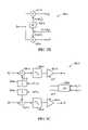
- FIG. 4shows an embodiment of transmitter 212 -k, an arbitrary one of transmitters 212 - 1 through 212 -K.
- Transmitter 212 -kreceives n k bits per baud interval, 1/B k , for transmission into sub-channel 301 -k.
- the n k bitsare received in scrambler 401 .
- Scrambler 401scrambles the n k bits and outputs a scrambled signal of n k bits, which “whitens” the data.
- encoder 402can be a trellis encoder for the purpose of providing error correction capabilities.
- Trellis codingallows for redundancy in data transmission without increase of baud rate, or channel bandwidth.
- Trellis codingis further discussed in, for example, B ERNARD S KLAR , D IGITAL C OMMUNICATIONS , F UNDAMENTALS AND A PPLICATIONS (Prentice-Hall, Inc.,1988), G. Ungerboeck., “Trellis Coding Modulation with Redundant Signal Sets, Part I. Introduction,” IEEE Communications Magazine, vol. 25, no. 2, February 1987, pp. 5-11, and G.
- encoder 402can be a trellis encoder which adds one additional bit, in other words encoder 402 can be a rate n k /n k +1 encoder, see, e.g., G. Ungerboeck., “Trellis Coding Modulation with Redundant Signal Sets, Part I. Introduction,” IEEE Communications Magazine, vol. 25, no. 2, February 1987, pp. 5-11, and G. Ungerboeck., “Trellis Coding Modulation with Redundant Signal Sets, Part II. State of the Art,” IEEE Communications Magazine, vol. 25, no. 2, February 1987, pp. 12-21.
- additional bitscan be added to insure a minimum rate of transitions so that timing recovery can be efficiently accomplished at receiver 220 -p.
- FIG. 6Ashows an embodiment of encoder 402 .
- Encoder 402 of FIG. 6Ais an n k /n k +1 trellis encoder.
- Encoder 402 of FIG. 6Aperforms a rate 1 ⁇ 2 convolutional coding on the most-significant-bit (MSB) of the n k bit input signal.
- the MSBis input to delay 601 .
- the output signal from delay 601is input to delay 602 .
- the MSB and the output signal from delay 602are input to XOR adder 603 .
- the output from XOR adder 603provides a coded bit.
- the MSB, the output signal from delay 601 , and the output signal from delay 602are XORed in adder 604 to provide another coded bit.
- the two coded bitsare joined with the remaining n k -1 bits to form a n k +1 bit output signal.
- Delays 601 and 602are each clocked at the symbol baud rate B.
- symbol mapper 403can include any symbol mapping scheme for mapping the parallel bit signal from encoder 402 onto symbol values for transmission.
- a trellis encoder in conjunction with a QAM mappercan provide a trellis encoded QAM modulation for sub-channel 301 -k.
- FIG. 6Bshows an embodiment of symbol mapper 403 .
- Symbol mapper 403receives the n k +1 data bits from encoder 402 and generates a symbol which can include an in-phase component I k and a quadrature component Q k .
- symbol mapper 403includes a look-up table 605 which maps the n k +1 input bits to the complex output symbol represented by I k and Q k .
- Table Ishows an example symbol look-up table for conversion of a 7-bit data signal into a 128-symbol QAM scheme.
- Table entriesare in decimal format with the in-phase values along the bottom row and the quadrature values represented along the last column. From Table I, a decimal value of 96, for example, results in an I value of ⁇ 1 and a Q value of ⁇ 1.
- the QAM mappingcan be segregated into groups of four as is shown in FIG. 6C .
- n k +1is 7.
- the two control bits from encoder 402are arranged so that in groups of four symbols, the two control bits determine placement in the group.
- Control bits 00 and 11 and control bits 01 and 10are in opposite corners of the groupings of four. This leads to a 6 dB gain in decoding at the receiver using this mapping scheme. Furthermore, the remaining five bits determine the actual grouping of four.
- the output signal from symbol mapper 403can be a complex signal represented by in-phase signal I k (n) and a quadrature signal Q k (n), where n represents the nth clock cycle of the clock signal CK 1 , whose frequency equals the baud rate B k .
- signals I k (n) and Q k (n)are digital signals representing the values of the symbols they represent.
- a QAM mapper onto a constellation with 128 symbolscan be utilized. An embodiment of a 128-symbol QAM constellation is shown in Table I.
- constellations and mappingsare well known to those skilled in the art, see, e.g., B ERNARD S KLAR , D IGITAL C OMMUNICATIONS , F UNDAMENTALS AND A PPLICATIONS (Prentice-Hall, Inc.,1988) and E. A. L EE AND D. G. M ESSERSCHMITT , D IGITAL C OMMUNICATIONS (Kluwer Academic Publishers, 1988).
- the number of distinct combinations of I k (n) and Q k (n)represents the number of symbols in the symbol set of the QAM mapping and their values represent the constellation of the QAM mapping.
- the signals from symbol mapper 403 , I k (n) and Q k (n),are input to digital-to-analog converters (DACs) 406 and 407 , respectively.
- DACs 406 and 407operate at the same clock rate as symbol mapper 403 . In some embodiments, therefore, DACs 406 and 407 are clocked at the symbol rate, which is the transmission clock frequency B k .
- the analog output signals from DACs 406 and 407can be input to low-pass filters 408 and 409 , respectively.
- Low pass filters 408 and 409are analog filters that pass the symbols represented by I k (t) and Q k (t) in the base band while rejecting the multiple frequency range reflections of the base band signal.
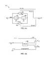
- FIG. 6Dshows a schematic diagram of the ideal requirements for filters 408 and 409 .
- the filter function h(f)cuts off to include all of the base band signal while rejecting all of the higher frequency reflections of the base band signal created by DACs 406 and 407 .
- filters 408 and 409can be described by a two-zero, five-pole filter function of the form
- H TX ⁇ ( s )b 2 ⁇ s 2 + b 1 ⁇ s + b 0 s 5 + a 4 ⁇ s 4 ⁇ ⁇ ⁇ + a 0 , ( 2 )
- si(2 ⁇ f) (i is ⁇ square root over ( ⁇ 1) ⁇ )
- the coefficients b 2 , b 1 , b 0 , and a 4 through a 0are the parameters of filters 408 and 409 .
- the parameters for filters 408 and 409can be found by minimizing the cost function
- H DAC (f)is the response of DACs 406 and 407 , which can be given by
- H DAC ⁇ ( f )sin ⁇ ( ⁇ ⁇ ⁇ fT k ) ⁇ ⁇ ⁇ f , ( 4 )
- T kis the symbol period
- W(f)is a weighting function
- H RRC (f)is a target overall response
- ⁇is the time delay on the target response.
- the cost functionis minimized with respect to the parameters of the filter (e.g., coefficients b 2 , b 1 , b 0 , and a 4 through a 0 ) and the time delay ⁇ .
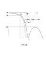
- FIG. 6Eshows an example of a target overall response function H RRC (f), which is a square-root raised cosine function.
- the function H FRC (f)can be determined by a parameter ⁇ k along with the baud rate frequency 1/T k (which is the baud rate B k for transmitter 212 -k).
- the parameter ⁇ kis the excess bandwidth of the target function H RRC (f).
- ⁇ kcan be set to 0.
- ⁇ kcan be set to 0.6.
- the weight function W(f)can be chosen such that the stop band rejection of H TX (s) is less than about ⁇ 50 dB. Initially, W(f) can be chosen to be unity in the pass band frequency 0 ⁇ f ⁇ (1+ ⁇ k )/2T k and zero in the stop band frequency f>(1+ ⁇ k )/2T k , where ⁇ k is the excess bandwidth factor of the kth channel. The minimization of the cost function of Equation 3 can be continued further by increasing W(f) in the stop band until the rejection of analog filters 408 and 409 is less than ⁇ 50 dB.
- the DAC response h k DAC (t)is a sinc function in the frequency domain and a rectangular pulse in the time domain.
- the overall responseis a convolution of filters 408 and 409 with the response of DACs 406 and 407 .
- the overall filter responsecan be close to the target response H RRC (f) when h k TX (t) is determined with the cost function of Equation 3.
- the output signals from low-pass filters 408 and 409are then up-converted to a center frequency f k to generate the output signal of y k (t), the kth channel signal.
- the output signal from low-pass filter 408 , I k LPF (t),is multiplied by cos (2 ⁇ f k t) in multiplier 410 .
- the output signal from low-pass filter 409 , Q k LPF (t)is multiplied by sin (2 ⁇ f k t) in multiplier 411 .
- the signal sin (2 ⁇ f k t)can be generated by PLL 414 based on the reference clock signal and the signal cos (2 ⁇ f k t) can be generated by a ⁇ /2 phase shifter 413 .
- mixers 410 and 411are typically not ideal mixers and the harmonic sine wave input to mixer 410 , and the resulting cosine wave input to mixer 411 , often varies from a sine wave, signals having harmonics of the frequency f k are also produced. Often, the harmonic signals input to mixers 410 and 411 may more closely resemble square-wave signals than harmonic sine wave signals. Even if the “sine wave input” is a true sine wave, the most commonly utilized mixers, such as Gilbert Cells, may act as a band-limited switch, resulting in a harmonic signal with alternating positive and negative voltages with frequency the same as the “sine wave input” signal.
- the output signals from filters 408 and 409are still multiplied by signals that more closely resemble square waves than sine waves.
- signals having frequency 2f k , 3f k , . . .are also produced, as well as signals in the base band (0f k ).
- the amplitude of these signalsmay be attenuated with higher harmonics, they are non-negligible in the output signal.
- even harmonicsi.e., 0f k , 2f k ,4f k . . .
- y k ⁇ ( t )⁇ ⁇ k 0 ⁇ I k LPF ⁇ ( t ) - ⁇ k 0 ⁇ Q k LPF ⁇ ( t ) + ⁇ n > 0 ⁇ ( ⁇ k n ⁇ I k LPF ⁇ cos ⁇ ( 2 ⁇ ⁇ ⁇ ⁇ nf k ⁇ t ) - ⁇ ⁇ k n ⁇ Q k LPF ⁇ sin ⁇ ( 2 ⁇ ⁇ ⁇ ⁇ nf k ⁇ t ) . ( 6 ) where ⁇ k n and ⁇ k n is the contribution of the nth harmonic to y k (t).
- the signal on channel oneis replicated into all of the K channels, the baseband, and into harmonic frequencies beyond the base band and the K channels.
- the signal on channel twofor example, is also transmitted on channels 4 , 6 , 8 , . . . , and the baseband.
- the signal on channel 3is transmitted on channels 6 , 9 , 12 , . . . and the base band.
- the signal on channel kwill be mixed into channels 2 k , 3 k , . . . and the baseband.
- the attenuation of the signals with higher harmonics in some systemscan be such that the signal from channel k is non negligible for a large number of harmonics, potentially up to the bandwidth of the process, which can be 30-40 GHz.
- a high pass filter 215receives the signal from summer 213 .
- High pass filter 215can, for example, be a first-order high-pass filter with 3 dB attenuation at f 1 /2.
- Filter 215removes the DC harmonics, i.e. the baseband transmissions, from the transmitter. In embodiments with a separate baseband transmission, then, cross-channel coupling into the baseband is minimized or eliminated. Further, removing the baseband harmonics from the transmitted signals simplifies cross-channel cancellation at receiver 220 -p.
- the first term of Equation 8the first term of Equation 8,
- ⁇ k1 K ⁇ ( ⁇ k 0 ⁇ I k LPF ⁇ ( t ) - ⁇ k 0 ⁇ Q k LPF ⁇ ( t ) ) , is filtered out and becomes close to 0.
- the output signal from transmitter 210 -pthen becomes
- the center frequencies of channels 301 - 1 through 301 -Kcan be any separated set of frequencies which substantially separate (i.e., minimizing overlap between channels) in frequency the transmission bands of transmission channels 301 - 1 through 301 -K.
- the frequencies f 1 through f Kare chosen as multiplies of a single frequency f 0 which can fulfill equations 10 and/or 11 and results in the harmonic mixing of channels as shown in Equation 8 and 9.
- DACs 406 and 407may be moved to receive the output of summer 412 . Further, in some embodiments DACs 406 and 407 can be replaced by a single DAC to receive the output of summer 213 . However, such DACs should have very high sampling rates. One advantage of utilizing high-sampling rate DACs is that ideal mixing could take place and the number of harmonics that need to be cancelled can be greatly reduced or even eliminated.
- an embodiment of transmitter 210 -p capable of 10 Gbps transmissioncan be formed.
- n k6;1 ⁇ k ⁇ 8 and encoder 402 is a 6/7 rate trellis encoder.
- symbol mapper 403can be a QAM symbol mapper with a 128-symbol constellation with baud rate B k .
- the baud rate B kthen, can be the same on all sub-channels 301 - 1 through 301 -K.
- DACs 406 and 407can have any resolution, limited only by the number of bits required to represent the symbol values output from symbol mapper 403 .
- DACs 406 and 407are each 4 bit DACs.
- a schematic diagram of an embodiment of trellis encoder 402 and an embodiment of the resultant 128-QAM constellation mappingare shown in FIGS. 6A , 6 B, and 6 C, respectively.
- An example of a 128 symbol QAM mapping tableis shown as Table I.
- the above described trellis encoder 402in this embodiment, provides an asymptotic coding gain of about 6 dB over uncoded 128-QAM modulation with the same data rate, see, e.g., G. Ungerboeck., “Trellis Coding Modulation with Redundant Signal Sets, Part I. Introduction,” IEEE Communications Magazine, vol. 25, no. 2, February 1987, pp. 5-11, and G. Ungerboeck., “Trellis Coding Modulation with Redundant Signal Sets, Part II. State of the Art,” IEEE Communications Magazine, vol. 25, no. 2, February 1987, pp. 12-21.
- FIG. 5Ashows an example of one of receiver systems 220 -p where receiver system 220 -p is an arbitrary one of receiver systems 220 - 1 through 220 -P of system 200 .
- Receiver system 220 -pincludes receivers 221 - 1 through 221 -K to form a K-channel receiver.
- the output signals from receiver input buffer 224 , Z(t)is received in each of receivers 222 - 1 through 222 -K.
- the signal Z(t)then, is the transmitted signal z(t) after transmission through medium 250 .
- the attenuation of signals at each of the K carrier frequencies after transmission through medium 250can be different.
- the signal Z(t)suffers from inter-symbol interference caused by the dispersive effects of medium 250 .
- the dispersive effectscause the signals received within a particular timing cycle to be mixed with those signals at that carrier frequency received at previous timing cycles. Therefore, in addition to cross-channel interference effects caused by the harmonic generation in mixers of the transmitter (an arbitrary one of which being designated transmitter 210 -p), but also the signals for each channel are temporally mixed through dispersion effects in medium 250 .
- Signal Z(t)is then received into each of receivers 222 - 1 through 222 -K.
- receiver 222 -kan arbitrary one of receivers 222 - 1 through 222 -K, for example, receives the signal Z(t) into down converter 560 -k which, in the embodiment shown in FIG. 5A , down converts the channel transmitted at frequency f k back into the base-band and recovers in-phase and quadrature components Z k 1 and Z k Q , respectively.
- FIG. 5Ashows an embodiment of down-converter 560 -k.
- Signal Z(t)is received in multipliers 501 -k and 502 -k where it is down-converted to baseband to obtain an in-phase component Z k 1 (t) and a quadrature component Z k Q (t).
- Multiplier 501 -kmultiplies signal Z(t) with cos (2 ⁇ k t) and multiplier 502 -k multiplies signal Z(t) with sin (2 ⁇ k t), where ⁇ circumflex over (f) ⁇ k can be the locally generated estimate of the carrier center frequency f k from the corresponding transmitter.
- the clock signals within component 201 -pan arbitrary one of components 201 - 1 through 201 -P, which are generated based on the reference signal from PLL 230 as shown in FIG. 2A , will have the same frequencies. However, the frequencies between differing ones of components 201 - 1 through 201 -P can be slightly different. Therefore, ⁇ f k ⁇ denotes the set of frequencies at the transmitter and ⁇ circumflex over (f) ⁇ k ⁇ denotes the set of frequencies at the receiver.
- component 201 -pis a slave component where the frequencies ⁇ circumflex over (f) ⁇ k ⁇ can be adjusted to match those of the component that includes the transmitter, which is also one of components 201 - 1 through 201 -P.
- component 201 -pis a master component, in which case the transmitter of the component communicating with component 201 -p adjusts frequencies ⁇ f k ⁇ to match those of ⁇ circumflex over (f) ⁇ k ⁇ .
- Arbitration in any given communication link between receiver 220 -p of component 201 -p and a transmitter in one of the other of components 201 - 1 through 201 -Pcan be accomplished in several ways.
- prioritymay be set between pairs of components 201 - 1 through 201 -P so that the master/slave relationship between those pairs is pre-determined.
- an overall system controlchooses at the start of each communication which component is master and which is slave.
- the two componentsmay negotiate, for example by each randomly choosing one of the k channels on which to transmit and designating the one that transmits on the lowest numbered channel as master. In any event, in any transmission either the transmitter adjusts ⁇ f k ⁇ or the receiver adjusts ⁇ circumflex over (f) ⁇ k ⁇ depending on which has been designated master and which slave upon start of the communications
- PLL 523generates the clock signals for each of receivers 222 - 1 through 222 -K and, in particular, generates the sin (2 ⁇ k t) signal for receiver 222 -k.
- the cos (2 ⁇ k t) signalcan be generated by ⁇ /2 phase shifter 524 -k.
- PLL 523generates the sampling clock signal utilized in analog to digital converters (ADCs) 506 -k and 507 -k as well as other timing signals utilized in receivers 222 - 1 through 222 -K.
- ADCsanalog to digital converters
- PLL 523also generates an RX CLK signal for output with the n k bit output signal from receiver 222 -k.
- Down converters 560 - 1 through 560 -Kalso generate harmonics for very much the same reasons that harmonics are generated in transmitters 212 - 1 through 212 -K. Therefore, down converter 560 -k will down-convert into the base band signals from signals having center frequencies 0, ⁇ circumflex over (f) ⁇ k , 2 ⁇ circumflex over (f) ⁇ k , 3 ⁇ circumflex over (f) ⁇ k , . . .
- the down conversion process for down converter 560 - 1will result in the output signals Z 1 I and Z 1 Q including interference contributions from the received signals from all of the other channels.
- the output signals Z 2 I and Z 2 Qinclude contributions from channels with frequencies 0, 2 ⁇ circumflex over (f) ⁇ 0 , 4 ⁇ circumflex over (f) ⁇ 0 , 6 ⁇ circumflex over (f) ⁇ 0 . . . and those channels with harmonics at these frequencies.
- each of the channelsalso include the cross-channel interference generated by the transmitter mixers and the dispersive interference created by the channel. If the baseband component of the harmonics is not filtered in filter 215 ( FIG. 2B ) out between the transmit and receive mixers, then every channel could put a copy of its transmit signal onto the baseband and every channel will receive the baseband signal at the receive side.
- PLL 523can be a free-running loop generating clock signals for receiver 222 -k based on a reference clock signal.
- transmitter 212 -k of transmitter and demodulator 222 -k of the receiver system 220 -pbecause they are part of different ones of components 201 - 1 through 201 -P, are at different clock signals. This means that the digital PLLs for timing recovery and carrier recovery correct both phase and frequency offsets between the transmitter clock signals and receiver clock signals.
- a transmitter/receiver pairi.e., transmitter 210 -p and receiver 220 -p of component 201 -p
- Components 201 -i and 201 -jwhere i and j refer to different ones of components 201 - 1 through 201 -P, in general may operate at different clock signal frequencies.
- the signals Z k 1 and Z k Q output from down converter 560 -ksuffer the effects of cross-channel interference resulting from harmonic generation in the transmitter mixers, the effects of cross-channel interference resulting from harmonic generation in the receiver mixers, and the effects of temporal, intersymbol interference, resulting from dispersion in the transport media.
- the transmitter and receiver clockscan be different.
- ⁇ circumflex over (f) ⁇ 1 through ⁇ circumflex over (f) ⁇ K of the receiverwill correspond to frequencies (f 0 + ⁇ ) through K(f 0 + ⁇ ), where ⁇ represents the frequency shift between PLL 523 of receiver 220 -p and the PLL of the transmitter component.
- the transmitter mixersthen cause cross-channel interference by mixing the signals transmitted at frequency f k into 2f k , 3f k . . . (2kf 0 , 3kf 0 . . . in one example).
- the receiver mixerscause cross-channel interference by down-converting the signals received at ⁇ circumflex over (f) ⁇ k , 2 ⁇ circumflex over (f) ⁇ k , 3 ⁇ circumflex over (f) ⁇ k . . . to the baseband. If the frequencies ⁇ circumflex over (f) ⁇ 0 is f 0 + ⁇ , then the harmonics will be down-converted to a base-band shifted in frequency by k ⁇ , 2k ⁇ , 3k ⁇ , . . . , respectively.
- receiver 220 -pincludes a frequency shift 563 which supplies a reference clock signal to PLL 523 .
- the reference clock signal supplied to PLL 523can be frequency shifted so that A becomes 0.
- the frequency supplied to PLL 523 by frequency shift 563can be digitally created and the input parameters to frequency shift 563 can be adaptively chosen to match the receiver frequency with the transmitter frequency. Embodiments of frequency adjustments in frequency shift 563 and PLL 523 are further discussed below.
- the output signals from down-converter 560 -k, Z k I and Z k Qare input to analog filter 561 - 2 .
- An embodiment of analog filter 561 - 2is shown in FIG. 5C .
- the signals Z k I and Z k Qare input to offset corrections 530 -k and 531 -k, respectively.
- DC offset corrections 530 -k and 531 -kprovide a DC offset for each of the outputs Z k I and Z k Q from down-converter 560 -k to correct for any leakage onto signal Z(t) from the sine and cosine signals provided by PLL 523 , plus any DC offset in filters 504 -k and 505 -k and ADCs 506 -k and 507 -k. Leakage onto Z(t) can, in some cases, provide a significant DC signal component of the output signals Z k I and Z k Q from down-converter 560 -k. In some embodiments, offsets 530 -k and 531 -k can offset by the same amount.
- different offset values, DCOI and DCOQ in FIG. 5Ccan be provided for each of the output signals Z k I and Z k Q from down-converter 560 -k.
- the DC offset valuescan be adaptively chosen in blocks 543 -k and 544 -k. In some embodiments, after an initial start-up procedure, the DC offset values are fixed.
- the DC offsets, DCOI and DCOQ inputs to offsets 530 -k and 531 -k, respectivelycan be generated by providing a low frequency integration of the output signal from analog-to-digital converters (ADCs) 506 -k and 507 -k ( FIG. 5A ).
- ADCsanalog-to-digital converters
- FIG. 5Cfor example, low-frequency integrator 543 -k receives the output signal from of ADC 506 -k, R k I , and provides the DCOI input signal to offset 530 -k; integrator 544 -k receives the output signal from ADC 507 -k, R k Q , and provides the DCOQ input signal to offset 531 -k.
- integrators 544 -k and 543 -kprovide signals that set the average output signal of each of ADCs 506 -k and 507 -k to zero.
- integrators 543 -k and 544 -khold the offset values DCOI and DCOQ, respectively, constant after a set period time of integration when receiver 222 -k is first started.
- Low-pass filters 504 -k and 505 -kare analog filters that filter out signals not associated with the baseband signal (i.e., signals from the remaining bands of transmitter 210 -p) for the kth transmission band.
- Low pass filters 504 -k and 505 -kdo not remove the interference caused by harmonic generation in transmit and receive mixers involved in the up-conversion and down-conversion process.
- Filters 504 -k and 505 -k againcan be parameterized by the two-zero, five-pole filter design described by Equation 2,
- H RX ⁇ ( s )b 2 ⁇ s 2 + b 1 ⁇ s + b 0 s 5 + a 4 ⁇ s 4 + ⁇ + a 0 . ( 12 ) Furthermore, the parameters b 2 , b 1 , b 0 , and a 4 through a 0 can be found by minimizing the cost function
- the function H RRC (f)is characterized by a parameter ⁇ k and baud frequency 1/T k .
- the parameter ⁇ kis the excess bandwidth of the target function H RRC (f).
- ⁇ kcan be 0.
- ⁇ kcan be 0.6.
- the parameter ⁇ kcan be any value, with smaller values providing better filtering but larger values being easier to implement.
- filters 504 -k and 505 -kcan be determined by minimizing the function
- Equation 14includes the effects of the transmit digital to analog converters 406 and 407 ( FIG. 4 ) as well as the analog transmit filters 408 and 409 ( FIG.
- H TX (f) and H RX (f)can be the same.
- the output signals from low-pass filters 504 -k and 505 -kcan, in some embodiments, be amplified in variable gain amplifiers 521 -k and 522 -k, respectively.
- the gains g k 1(I) and g k 1(Q) of amplifiers 521 -k and 522 -k, respectivelyare set such that the dynamic range of analog-to-digital converters 506 -k and 507 -k, respectively, is filled.
- the gains of amplifiers 521 -k and 522 -kcan be set in an automatic gain control circuit (AGC) 520 -k.
- AGCautomatic gain control circuit
- FIGS. 8A and 8BAn embodiment of automatic gain circuit 520 -k where g k 1(I) and g k 1(Q) are set equal to one another is shown in FIGS. 8A and 8B .
- amplifiers 521 -k and 522 -kcan be before or incorporated within filters 504 -k and 505 -k, respectively.
- the signals output from analog filter 561 -k, signals r k I (t) and r k Q (t),are input to analog-to-digital converters (ADC) 506 -k and 507 -k, respectively, which forms digitized signals R k I (t) and R k Q (t) corresponding with the analog signals r k I (t) and r k Q (t), respectively.
- ADCs 506 -k and 507 -koperate at a sampling rate that is the same as the transmission symbol rate, e.g. the QAM symbol rate.
- ADCs 506 -k and 507 -kcan operate at higher rates, for example twice the QAM symbol rate.
- the timing clock signal SCLK, as well as the sine and cosine functions of Equation 15,is determined by PLL 523 .
- ADCs 506 -k and 507 -kcan be 8-bit ADCs. However, for 128 QAM operation, anything more than 7 bits can be utilized.
- the gain of amplifiers 521 -k and 522 -k of analog filters 560 -kcan be set by automatic gain control circuit (AGC) 520 -k (see FIG. 5C ).
- Gain control circuit 520 -kcan receive the digital output signals from ADCs 506 -k and 507 -k, R k I (n) and R k Q (n), respectively, and determines the gain g 1 k (n+1) for each of amplifiers 521 -k and 522 -k (i.e., in this embodiment g 1(I) k (n) and g 1(Q) k (n) are equal).
- FIGS. 8A and 8Bshow some embodiments of AGC 520 -k.
- AGC 520 -k shown in FIG. 8Aincludes an AGC phase detector 801 and an integrator 802 .
- Phase detector 801estimates whether or not the mean-squared-power of signals R k I (t) and R k Q (t) are at a pre-determined threshold value and, if not, provides a correction signal to adjust the amplitudes of signals r k I (t) and r k Q (t).
- the output signal from phase detector 801 , p k g (n)is then input to integrator 802 .
- the constant ⁇ gcan be chosen to be a negative power of 2 for ease of implementation.
- phase detector 520 -k shown in FIG. 8Bincludes two phase detectors 803 and 804 which calculate the mean squared powers of R k I (n) and R k Q (n) separately and compare them with thresholds G th I and G th Q respectively.
- P k g-Q ( n )[G th Q ⁇ ( R k Q ( n ) 2 )], (18) respectively.
- AGC 520 -kcan include a peak detection algorithm so that the gain values g k 1(I) and g k 1(Q) are determined from the peak values of R k I and R k Q , respectively. Again, the peak values of R k I and R k Q can be compared with threshold values and the gain values g k 1(I) and g k 1(Q) adjusted accordingly.
- the output signals from ADCs 506 -k and 507 -k, R k I and R k Q , respectively,are input to a first digital filter 562 -k.
- An embodiment of first digital filter 562 -kis shown in FIG. 5D .
- the in-phase and quadrature data pathsmay suffer from small differences in phase and small differences in gain. Therefore, in some embodiments a phase and amplitude correction is included in digital filter 562 -k. In order to correct the phase and amplitude between the in-phase and quadrature data paths, one of the values R k I (n) and R k Q (n) is assumed to be of the correct phase and amplitude. The opposite value is then corrected.
- R k I (n)is assumed to be correct and R k Q (n) is corrected.
- the phase errorcan be corrected by using the approximation for small ⁇ k c where sin ⁇ k c is approximately ⁇ k c , and cos ⁇ k c is approximately one.
- This correctioncan be implemented by subtracting in summer 536 -k the value ⁇ k c R k I (n) calculated in multiplier 535 -k to R k Q (n).
- the amplitude of R k Q (n)can be corrected by adding a small portion ⁇ k c of R k Q (n), calculated in multiplier 533 -k, in summer 536 -k.
- the value ⁇ k ccan be determined in tracking and recovery block 517 -k by integrating the difference in magnitude of the output signals from summer 534 -k and 536 -k, F k I (n) and F k Q (n), in a very low frequency integration block (for example several kHz), such that
- ⁇ k c⁇ ( ⁇ F k l ⁇ ( n ) ⁇ - ⁇ F k Q ⁇ ( n ) ⁇ ) ⁇ d n .
- an arithmetic offsetcan be implemented by subtracting the value OFFSET 1 I in summer 534 -k to R k I (n) and subtracting the value OFFSET 1 Q in summer 536 -k.
- the offset values OFFSET 1 I and OFFSET 1 Qcan be adaptively chosen in tracking and recovery block 517 -k by integrating the output signals from summer 534 -k and summer 536 -k, F k I (n) and F k Q (n), respectively, in a low frequency integration.
- the offsets implemented in summer 534 -k and 536 -koffset the dc offset not corrected in analog filter 561 -k, e.g. by offsets 530 -k and 531 -k, for example, as well as arithmetic errors in summers 534 -k, 536 -k and multipliers 535 -k and 533 -k.
- the parameters OFFSET 1,k I , OFFSET 1,k Q , ⁇ k c , and ⁇ k cvary for each cycle n. Additionally, the parameters can be different for each of the k receivers 222 - 1 through 222 -k.
- phase rotation circuit 512 -krotates signals F k I (n) and F k Q (n) according to the output of a carrier phase and frequency offset correction circuit, which depends on the difference between ⁇ circumflex over (f) ⁇ k and ⁇ circumflex over (f) ⁇ k , and the relative phase of the transmit mixers (multipliers 410 and 411 ) and the receive mixers (multipliers 501 -k and 502 -k) and transmission channel 250 ( FIG.2A ).
- the rotation angle ⁇ circumflex over ( ⁇ ) ⁇ k I (n)is computed in carrier tracking and timing recovery block 517 .
- the output signals from rotation circuit 512 -k, D k I (n) and D k Q (n),are then input to a complex adaptive equalizer 513 -k to counter the intersymbol interference caused by frequency dependent channel attenuation, and the reflections due to connectors and vias that exist in communication system 200 (which can be a backplane communication system, an inter-cabinet communication system, or a chip-to-chip communication system) and both transmit and receive low pass filters, e.g. filters 408 and 409 of FIG. 4 and filters 504 -k and 505 -k of FIG. 5C .
- equalizer 513can have any number of taps.
- Complex Equalizer 513 -kcan be either a linear equalizer (i.e., having a feed-forward section only) or a decision feed-back equalizer (i.e., having a feed-forward and a feedback portion).
- the coefficients of the equalizer transfer functionare complex-valued and can be adaptive.
- the complex equalizer coefficients that operate on signals D k I and D k Qare the same, but in other embodiments the complex equalizer coefficients are allowed to be different for D k I and D k Q .
- the feed-forward portion of an adaptive equalizercan be preceded by a non-adaptive all-pole filter with transfer function 1/A(z).
- a ⁇ ( Z )1 + 0.75 ⁇ ⁇ Z - 1 + 1 16 ⁇ Z - 2 + ( 1 64 + 1 128 ) ⁇ Z - 3 + ( 1 16 + 1 32 ) ⁇ Z - 4 .
- complex adaptive equalizer 513 -kcan be a decision feedback equalizer (DFE) or a linear equalizer. See, e.g., E DWARD A. L EE, AND D AVID G. M ESSERSCHMITT , D IGITAL C OMMUNICATION, PP. 371-402 (Kluwer Academic Publishers, 1988).
- DFEdecision feedback equalizer
- linear equalizere.g., E DWARD A. L EE, AND D AVID G. M ESSERSCHMITT , D IGITAL C OMMUNICATION, PP. 371-402 (Kluwer Academic Publishers, 1988).
- the in-phase and quadrature output signals from adaptive equalizer 513 in embodiments with linear equalizationcan be given by:
- the complex adaptive equalizer coefficients C k xI (j,n), C k y,I (j,n), C k x,Q (j,n) and C k y,Q (j,n)can be updated according to the least mean squares (LMS) algorithm as described in B ERNARD S KLAR , D IGITAL C OMMUNICATIONS , F UNDAMENTALS AND A PPLICATIONS (Prentice-Hall, Inc., 1988), for example.
- LMSleast mean squares
- equalizer coefficients C k x,I (j,n) and C k x,Q (j,n)are the same and equalizer coefficients C k y,I (j,n) and C k y,Q (j,n) are the same.
- the center coefficients of the feed-forward part of equalizer 513 -k, C k x,I (0,n), C k y,I (0,n), C k x,Q (0,n) and C k y,Q (0,n)can each be fixed at 1 and 0, respectively, to avoid interaction with the adaptation of gain coefficients g k 2(I) and g k 2(Q) used in amplifiers 537 -k and 538 -k of a second digital filter 563 -k and the carrier phase correction performed in phase rotator 512 -k.
- the coefficients C k x,I ( ⁇ 1,n), C k y,I ( ⁇ 1,n), C k x,Q ( ⁇ 1,n) and C k y,Q ( ⁇ 1,n)can be fixed at constant values to avoid interaction with the adaptation of the phase parameter ⁇ circumflex over ( ⁇ ) ⁇ k by tracking and timing recovery 517 -k.
- the parameters C k x,I ( ⁇ 1,n) and C k x,Q ( ⁇ 1,n)can be ⁇ 1 ⁇ 4- 1/16, which is ⁇ 0.3125
- the parameters C k y,Q ( ⁇ 1,n) and C k y,Q ( ⁇ 1,n)can be ⁇ 1/64, which is ⁇ 0.015625.
- one set of parametersfor example C k x,I ( ⁇ 1,n) and C k x,Q ( ⁇ 1,n) are fixed while the other set of parameters, for example C k y,I ( ⁇ 1,n) and C k y,Q ( ⁇ 1,n), can be adaptively chosen.
- C k x,I ( ⁇ 1,n) and C k y,I ( ⁇ 1,n)are fixed and the timing recover loop of adaptive parameters 517 - 2 for determining the phase parameter ⁇ circumflex over ( ⁇ ) ⁇ k utilizes errors e k I only (see FIG. 7 ). In that way, adaptively choosing parameters in the Q channel do not interact with the timing loop.
- the oppositecan be utilized (i.e., C k x,Q ( ⁇ 1,n) and C k y,Q ( ⁇ 1,n) are fixed and the timing loop determines the phase parameter ⁇ circumflex over ( ⁇ ) ⁇ k from error parameter e k Q .
- cross-channel interference filter 570removes the effects of cross-channel interference.
- Cross-channel interferencecan result, for example, from harmonic generation in the transmitter and receiver mixers, as has been previously discussed.
- equalization for intersymbol interferencecan be performed in digital filter 562 -k.
- cross-channel interference filter 570may be placed before equalizer 513 -k (in other words, equalizer 513 -k may be placed in digital filter 563 - 2 instead of digital filter 562 - 2 ).
- the output signals from digital filter 562 - 2 , E k I (n) and E k Q (n), for each of receivers 222 - 1 through 222 -Kare input to cross-channel interference filter 570 .
- An embodiment of cross-channel interference canceller 570is shown in FIG. 5F .
- Each of the complex values E 1 through E Kis input to a summer 571 - 1 through 571 -K, respectively, where contributions from all of the other channels are removed.
- the output signals from summers 571 - 1 through 571 -K, H 1 through H K , respectively,are the output signals from cross-channel interference filter 570 .
- the complex value H k (n)is H k I (n)+iH k Q (n), representing the in-phase and quadrature output signals.
- the signal E kis also input to blocks 572 -k, 1 through 572 -k,k ⁇ 1 and blocks 572 -k,k+1 to 572 -k,K.
- Block 572 -k,lan arbitrary one of blocks 572 - 1 , 2 through 572 -K, K-1, performs a transfer function Q k,l which determines the amount of signal E k which should be removed from E 1 to form H l .
- delays 573 - 1 through 573 -Kdelay signals E 1 through E K for a set number of cycles N to center the cancellations in time. Therefore, the output signals H l through H K can be determined as
- each of the functions Q k,lcan have a different number of taps M and N can be different for each channel
- the number of taps M for each function Q k,lcan be the same.
- delayscan be added in order to match the timing between all of the channels.
- delays 573 - 1 through 573 -Kcan delay signals E 1 through E K by a different number of cycles.
- the coefficients ⁇ k,l 0 through ⁇ k,l Mcan be adaptively chosen in cross-channel adaptive parameter block 571 as shown in FIG. 5A in order to optimize the performance of receiver system 220 -p.
- Mis chosen to be 5.
- Cross-channel adaptive parameter block 571is further discussed below.
- cross channel interference canceller 570the cross channel interference is subtracted from the output signals from digital filters 562 - 1 through 562 -K as indicated by Equation 26.
- An embodiment of second digital filter 563 -kis shown in FIG. 5E .
- the parameters ⁇ k,l m of Equation 28can be adaptively chosen. In the adaptation algorithm, the real and imaginary parts of ⁇ k,l m can be adjusted separately. The adaptive adjustments of parameters a ⁇ k,l m is further discussed below.
- the signals H k I and H k Qcan be input to AGC controlled amplifiers 537 -k and 538 -k, respectively.
- the gains of amplifiers 537 -k and 538 -k, g k 2(I) and g k 2(Q) , respectively,are set such that the output signals from amplifiers 537 -k and 538 -k yield appropriate levels for the symbol set.
- the gain values g k 2(I) and g k 2(Q)are set in tracking and timing recovery 517 -k and can be determined in much the same fashion as in AGC 520 -k of FIG. 5C .
- the gain values g k 2(I) and g k 2(Q)are determined based on the sign of the determined symbol from decision unit 516 -k and the error signal.
- Quadrature correction 540 -kcorrects for the phase error between the in-phase and quadrature mixers at the transmitter.
- the angle ⁇ circumflex over ( ⁇ ) ⁇ k (2) (n) of the phase errorcan be adaptively chosen in tracking and timing recovery 517 .
- the value ⁇ circumflex over ( ⁇ ) ⁇ k (2) (n)can be changed very slowly and can be almost constant.
- arithmetic offsets OFFSET 2 I and OFFSET 2 Qcan be subtracted in summers 541 -k and 542 -k, respectively.
- the values of OFFSET 2 I and OFFSET 2 Qcan be adaptively chosen in tracking and timing recovery 517 -k.
- the OFFSET 2 I and OFFSET 2 Qcan be set by integrating the output signals of summers 541 -k and 542 -k, G k I (n) and G k Q (n), respectively.
- OFFSET 2 I and OFFSET 2 Qcan be set such that the error at decision unit 516 -k is zero. In that embodiment, data dependent jitter can be reduced.
- tracking and timing recovery 517 -kintegrates the error values between the output samples from decision unit 516 -k and the output signals G k I (n) and G k Q (n) to minimize the error values.
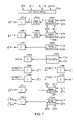
- FIG. 7shows an embodiment of Tracking and Timing Recovery 517 -k.
- Tracking and timing recovery 517 -kinputs decision values â k I (n) and â k Q (n), which are decisions of the symbol values based on the signals G k I (n) and G k Q (n) in decision unit 516 -k, and error values e k I (n) and e k Q (n) based on the decided values â k I (n) and â k Q (n) and the values G k I (n) and G k Q (n).
- the error values e k I (n) and e k Q (n)are the differences between the decided values â k I (n) and â k Q (n) and the values G k I (n) and G k Q (n).
- the coefficients of equalizer 513 -k of first digital filter 562 -kare computed in coefficient update 702 -k.
- the constant ⁇is chosen to control the rate of adaptation, and, in some embodiments, is in the range of 2 ⁇ 8 to 2 ⁇ 14 .
- the coefficient ⁇can be different for the update equation for C k x and the update equation for C k y .
- a decision set ⁇ â k I (n), â k Q (n) ⁇can be computed based on sample set ⁇ G k I (n), G k Q (n) ⁇ in decision unit 516 -k and the results received into tracking and timing recovery circuit 517 where the estimated error values of Equation 30 and the resulting coefficient updates of Equation 30 are computed.
- FIG. 7shows a block diagram of equalizer coefficient update, carrier tracking and timing recovery block 517 -k.
- Block 517 -kincludes coefficient update block 702 -k. Errors e k I (n) and e k Q (n) are computed in decision block 516 -k according to Equation 30.
- Coefficient update 702 -kreceives errors e k I (n) and e k Q (n) signals D k I (n) and D k Q (n) from phase rotator circuit 512 -k shown in FIG. 5D and calculates updated equalizer coefficients for complex adaptive equalizer 513 -k shown in FIG. 5D according to Equation 30.
- Tracking and timing recovery circuit 517 -kcan also include a carrier recovery loop for controlling carrier phase rotation circuit 512 -k shown in FIG. 5D and a timing recovery loop for controlling the phase of sampling clock signal SCLK from PLL 523 .
- the timing recovery loop for determining ⁇ k (n+1) in tracking and timing recovery 517can be implemented as a 2 nd order digital phase locked loop as shown in FIG. 7 .
- the phase correction ⁇ circumflex over ( ⁇ ) ⁇ kis calculated from e k I only or from e k Q only, as discussed above, then the terms containing e k Q or the terms containing e k I , respectively, are dropped from Equations 32 and 33.
- the output signal from phase detector 703 -k, p k ⁇can then be input to a 2 nd order loop filter, which in some embodiments can have a transfer function given by
- L ⁇ ( z )⁇ ⁇ + ⁇ ⁇ ⁇ z - 1 1 - z - 1 ( 34 )
- ⁇ ⁇ and ⁇ 96are the loop filter coefficients that determine the timing recovery loop bandwidth and damping factor.
- a loop bandwidthequal to 1% of baud rate, and damping factor equal to 1 can be implemented.
- the loop bandwidth and damping factorscan depend not only on loop filter coefficients, but also on phase detector slope, and the digital integrator gain.
- phase correction ⁇ circumflex over ( ⁇ ) ⁇ k (n)is then received by PLL 523 , as described above.
- phase detector 704 -kreceives decision values ⁇ â k I (n),â k Q (n) ⁇ and error signals ⁇ e k I (n),e k Q (n) ⁇ from decision unit 516 -k, and produces an estimate of the phase error.
- the estimate of the phase error p k ⁇ (n) performed by phase detector 704 -kcan be given by:
- the output signal from phase detector 704 -kcan be input to a 2 nd order loop filter 706 -k with a transfer function given by
- L ⁇ ( z )⁇ ⁇ + ⁇ ⁇ ⁇ z - 1 1 - z - 1 , ( 39 )
- ⁇ ⁇ and ⁇ ⁇are the loop filter coefficients that determine the carrier tracking loop bandwidth and the damping factor.
- the output signal from loop filter 706 -kis then input to a digitally implemented integrator 708 -k.
- the parameter ⁇ k c (n+1)can be calculated by phase detector 720 -k and integrator 722 -k as described in Equation 21.
- the parameter ⁇ k c (n+1) input into multiplier 533 -k shown in FIG. 5D .can be calculated by blocks 723 and integration block 724 according to Equation 20.
- the offset values OFFSET 2 I and OFFSET 1 Q input to summers 534 -k and 536 -k, respectively, of the embodiment of digital filter 562 -k shown in FIG. 5Dcan be determined by integrating the signals F k I (n) and F k Q (n), respectively.
- the offset values OFFSET 2 I , and OFFSET 2 Q input to summers 541 -k and 542 -k, respectively, of digital filter 563 -k shown in FIG. 5Ecan be calculated by integrating the signals G k I (n) and G k Q (n), respectively.
- the embodiment of adaptive parameter block 517 -k shown in FIG. 7calculates OFFSET 2 I and OFFSET 2 Q by integrating the error signals e k I (n) and e k Q (n), respectively.
- the coefficient ⁇ circumflex over ( ⁇ ) ⁇ k (2) to quadrature correction 540 -k of FIG. 5Ecan be calculated by phase detector 729 -k and integrator 731 -k.
- the gains g k 2-I and g k 2-Qcan be calculated by phase detector 732 and integrator 734 .
- cross-channel adaptive parameter block 571adaptively adjusts the parameters of cross-channel interference canceller 570 , all of the ⁇ k,l 1 parameters of Equations 26 and 27.
- all of complex parameters ⁇ k,l Jcan be set to 0.
- frequency shift 563generates a reference signal input to PLL 523 such that the frequency of component 201 -p with receiver system 220 -p, ⁇ circumflex over (f) ⁇ l through ⁇ circumflex over (f) ⁇ K , matches the frequency of the corresponding component 201 -q with transmitter system 210 -q, f 1 through f K , where component 201 -q is transmitting data to component 201 -p.
- frequency shift 563shifts the frequency of a reference clock such that the frequency shift ⁇ is zero.
- frequency shift 563can receive input from any or all loop filters 706 -k ( FIG. 7 ) and adjusts the frequency shift such that ⁇ circumflex over ( ⁇ ) ⁇ k (l) through ⁇ circumflex over ( ⁇ ) ⁇ k (K) remain a constant, for example 0 or any other angle. In some embodiments, frequency shift 563 receives the output signals from any or all loop filters 70 k.
- the output signals from digital filter 563 -k, equalized samples ⁇ G k I (n), G k Q (n) ⁇ ,are input to trellis decoder 514 -k.
- Trellis decodingcan be performed using the Viterbi algorithm, see, e.g., G. Ungerboeck., “Channel Coding with Multilevel/Phase Signals,” IEEE Transactions on Information Theory, vol. IT-28, January 1982, pp. 55-67, G. Ungerboeck., “Trellis Coding Modulation with Redundant Signal Sets, Part I. Introduction,” IEEE Communications Magazine, vol. 25, no. 2, February 1987, pp. 5-11, G.
- trellis decoder 514converts from the QAM symbol set back to parallel bits.
- the output signal from trellis decoder 514which now contains n k parallel bits, is input to descrambler 515 -k.
- Descrambler 515 -k of receiver demodulator 222 -koperates to reverse the scrambling operation of scrambler 401 of transmitter modulator 212 -k.
- the output signals from each of demodulators 222 - 1 through 222 -Kare recombined into an N-bit parallel signal in bit parsing 221 . Additionally, the RX clock signal is output from bit parsing 221 .
- FIG. 10shows an example embodiment of trellis decoder 514 according to the present invention.
- Trellis decoder 514 of FIG. 10Aincludes a slicer 1001 , a branch metric 1002 , an add-compare-select (ACS) block 1003 , a normalization and saturation block 1004 , a trace back 1005 , and a trellis decision block 1006 .
- the output signal from trellis decoder 514is the received bits, which are substantially as transmitted by transmitter 210 -p.
- Slicer 1001receives the output signals G k l (n) and G k Q (n) from offset blocks 541 and 542 , respectively.
- FIG. 10Bshows an embodiment of slicer 1001 .
- the value G k I (n)is received in x and y slicers 1010 and 1011 , respectively.
- Slicer 1010slices G k I (n) to a first set of symbol values while slicer 1011 slices G k I (n) to a second set of slicer values.
- x-slicer 1010can slice to the symbol values ⁇ 11, ⁇ 7, ⁇ 3, 1, 5, and 9 and y-slicer 1011 can slice to the symbol values ⁇ 9, ⁇ 5, ⁇ 1, 3, 7, 11.
- the number of bitscan be reduced by mapping the decided symbols from slicers 1010 and 1011 using table 1016 and 1021 , respectively.
- the output signal from tables 1016 and 1021are i x and i y , indicating decisions based on the input value G k I (n).
- the errors ⁇ i x and ⁇ i yare also calculated.
- the output signals from slicers 1010 and 1011are subtracted from the input signal G k I (n) in summers 1015 and 1020 , respectively.
- the output signals from slicers 1010 and 1011are input to blocks 1014 and 1019 , respectively, before subtraction in summers 1015 and 1020 .
- Blocks 1014 and 1019represent shifts.
- the input signals to slicers 1010 and 1011are 8-bit signed numbers. The value 8 slices to a perfect 1. Similarly, the value ⁇ 56 slices to a perfect ⁇ 7. So if the input signal is a ⁇ 56 it would be sliced to ⁇ 7. To calculate the error, we need to multiply the ⁇ 7 by 8 before it is subtracted from the incoming signal. Multiplying by 8 is the same as a shift to the left by 3.
- the absolute values of the output signals from summers 1015 and 1020are then taken by blocks 1017 and 1022 , respectively.
- the output signal from ABS blocks 1017 and 1022can be mapped into a set of values requiring a smaller number of bits by tables 1018 and 1023 , as in Table II above, respectively, to generate ⁇ i x and ⁇ i y , respectively.
- the output signals corresponding to the quadrature data path, q x , q y , ⁇ q x and ⁇ q yare generated by substantially identical procedure by slicers 1012 , 1013 , summers 1025 , 1030 , and blocks 1024 , 1026 , 1027 , 1028 , 1029 , 1031 , 1032 and 1033 .
- Branch metric 1002receives the error signals from slicer 1001 and calculates the signals ⁇ a, ⁇ b, ⁇ c, and ⁇ d.
- the branch metric values ⁇ a, ⁇ b, ⁇ c, and ⁇ dindicate the path metric errors.
- Add-Compare Select 1003receives the path metrics ⁇ a, ⁇ b, ⁇ c, and ⁇ d along with state metric values s 0 , s 1 , s 2 and s 3 , which are calculated in normalization and saturation block 1004 .
- the output values of ACS 1003include path metrics p 0 , p 1 , p 2 and p 3 along with choice indicators c 0 , c 1 , c 2 and c 3 .
- the choice indicators c 0 , c 1 , c 2 and c 3indicate which of the values was chosen in each of the minimization in Equation 43.
- Normalization and saturation 1004receives the path metrics p 0 , p 1 , p 2 and p 3 and calculates the state metrics s 0 , s 1 , s 2 and S 3 . In some embodiments, if the path metrics are above a threshold value, the threshold value is subtracted from each of the path metrics. In some embodiments, the smallest path metric can be subtracted from each of the path metrics p 0 , p 1 , p 2 and p 3 . Normalization and Saturation block 1004 also ensures that path metrics p 0 , p 1 , p 2 and p 3 are limited to a maximum value.
- p 0 , p 1 , p 2 and p 3are a four-bit number (range 0-15)
- p 0 , p 1 , p 2 or p 3is greater than 15
- the corresponding path metricis limited to the maximum value of 15.
- the state metrics for the next baud period, s 0 , s 1 , s 2 , and s 3are set to the path metrics p 0 , p 1 , p 2 and p 3 .
- Traceback 1005receives and stores the choice indicators c 0 , c 1 , c 2 and c 3 as well as the decided values from slicer 1001 in that baud period, i x , i y , q x , and q y .
- the choice indicators c 0 , c 1 , c 2 and C 3indicate the previous state values. As shown in the state transition diagram of FIG. 10C , which indicates state transitions between the encoded bits, for each of the states 0-3, there are only two possible previous states 0-3. For example, if the current state is 1, the previous state was either 0 or 2. Although any traceback depth can be utilized in traceback 1005 , in some embodiments a traceback depth of 6 is utilized.
- mapping tables 1016 , 1021 , 1026 and 1031reducing the number of bits required to store i x , i y , q x , and q y , (for example a total of 8 in 128 QAM systems) and the low number of bits required to store choice indicators c 0 , c 1 , c 2 and c 3 , a low number of bits is needed. For example, in some embodiments a total of 12 bits is utilized.
- the most recently stored memory locationsare utilized first with the first choice being the state with the lowest state metric.
- the algorithmthen traces back through the stored choice indications c 0 , c 1 , c 2 and c 3 to the end of the traceback memory (in some embodiments, the sixth state) and arrives at state S.
- the MSB of the outputis the LSB of the state, S.
- the final state S and the choice indicator c Swill determine which pair of symbols were transmitted (I x /I y , Q x /Q y ).
- FIG. 9shows a transceiver chip 900 according to the present invention.
- Transceiver chip 900includes transmitter 210 -p and receiver 220 -p formed on a single semiconductor chip.
- transceiver chip 900is formed in silicon using CMOS technology.
- Transceiver chip 900can receive N bits into transmitter 210 -p and output N bits from receiver 220 -p.
- different pinsmay be utilized for input bits and output bits, as shown in FIG. 9 .
- transmitter 210 -p and receiver 220 -pshare the same N pins.
- Transmitter 900receives a reference clock signal and outputs a receive clock signal from receiver 220 -p.
- transceiver 220includes output pins for transmitting and receiving differential signals.
- transmitter 210 -p and receiver 220 -pshare the same output pins and in some embodiments transmitter 210 -p and receiver 220 -p are coupled to separate output pins.
- transceiver chip 900may be coupled to an optical driver for optical transmission.
Landscapes
- Engineering & Computer Science (AREA)
- Computer Networks & Wireless Communication (AREA)
- Signal Processing (AREA)
- Digital Transmission Methods That Use Modulated Carrier Waves (AREA)
Abstract
Description
is greater than N.
where nkis the number of bits transmitted through the kth transmission band, centered about frequency fk, with a symbol baud rate on the kthsub-channel being equal to Bk.
where s=i(2πf) (i is √{square root over (−1)}) and the coefficients b2, b1, b0, and a4through a0are the parameters of
where HDAC(f) is the response of
where Tkis the symbol period, W(f) is a weighting function, HRRC(f) is a target overall response and τ is the time delay on the target response. The cost function is minimized with respect to the parameters of the filter (e.g., coefficients b2, b1, b0, and a4through a0) and the time delay τ.
hkTx(t)=hkf(t)⊕hkDAC(t), (5)
where hkf(t) is the response of the filter and hkDAC(t) is the response of
where ξknand ζknis the contribution of the nth harmonic to yk(t). If the duty cycle of the harmonic input signals to
where ω0is 2πf0and where IkLPF(t) and QkLPF(t) are 0 for all k>K.
is filtered out and becomes close to 0. The output signal from transmitter210-p then becomes
fk=Bkk(1+γk);1≦k≦K. (10)
In some embodiments, other center frequencies can be chosen, for example:
f1≧0.5Bk(1+βk)
(fk−fk-1)≧Bk(1+γk);k≧2 (11)
The parameter γkis the excess bandwidth factor. The bandwidth of the k-th channel, then, is (1+γk)Bk. In general, the center frequencies of channels301-1 through301-K can be any separated set of frequencies which substantially separate (i.e., minimizing overlap between channels) in frequency the transmission bands of transmission channels301-1 through301-K.

Furthermore, the parameters b2, b1, b0, and a4through a0can be found by minimizing the cost function
The cost function is minimized with respect to the parameters of the filter and the time delay τ. Again in
where the function HRC(f) is a square-root raised cosine function. The function HRC(f) is characterized by the parameters αkand 1/Tk. Equation 14 includes the effects of the transmit digital to
rkI(t)=LPF[Z(t) cos (2π{circumflex over (f)}kt)]gk1(I)
rkQ(t)=LPF[Z(t) sin (2π{circumflex over (f)}kt)]gk1(Q), (15)
where gk1(I)and gk1(Q)represents the gain of amplifiers521-k and522-k, respectively. The gains of amplifiers521-k and522-k can be set in an automatic gain control circuit (AGC)520-k. An embodiment of automatic gain circuit520-k where gk1(I)and gk1(Q)are set equal to one another is shown in
Pkg(n)=[Gth−(RkI(n)2+RkQ(n)2)], (16 )
where Gthis the mean squared power of the signals input to ADCs506-k and507-k once AGC520-k converges. The output signal from
gk1(n+1)=gk1(n)+αgPkg(n), (17)
where αgdetermines the rate of adaptation of the AGC algorithm. The constant αgcan be chosen to be a negative power of 2 for ease of implementation.
Pkg-I(n)=[GthI−(RkI(n)2)]
Pkg-Q(n)=[GthQ−(RkQ(n)2)], (18)
respectively. The output signals from
gk1-I(n+1)=gk1-I(n)+αgIpkg-I(n), and
gk1-Q(n+1)=gk1-Q(n)+αgQpkg-Q(n), (19)
where αgIand αgQdetermine the rate of adaptation of the AGC algorithm as in Equation 17 above.
The value θkccan be chosen in tracking and recovery block517-k by
θkc=∫(sign(FkI(n))FkQ(n)+sign(FkQ(n))FkI(n))dn. (21)
FkI(n)=RkI(n)−OFFSET1,KI,and
FkQ(n)=(1+ηkc)RkQ(n)−θkcRkI(n)−OFFSET1,kQ. (22)
In some embodiments, the parameters OFFSET1,kI, OFFSET1,kQ, ηkc, and θkcvary for each cycle n. Additionally, the parameters can be different for each of the k receivers222-1 through222-k.
DkI(n)=FkI(n) cos ({circumflex over (θ)}kI(n))+FkQ(n) sin ({circumflex over (θ)}kI(n))
DkQ(n)=FkQ(n) cos ({circumflex over (θ)}kI(n))−FkI(n) sin ({circumflex over (θ)}kI(n)). (23)
A(Z)=1.0+0.75Z−1+0.0625Z−2+0.0234375Z−3+0.09375Z−4, (24)
which can be rewritten as
The resulting transfer function H(z)=1/A(z) can be implemented in a linear equalizer or a decision feedback equalizer. In some embodiments, however, complex adaptive equalizer513-k includes adaptively chosen parameters.
where j refers to the tap Z−j. The complex adaptive equalizer coefficients CkxI(j,n), Cky,I(j,n), Ckx,Q(j,n) and Cky,Q(j,n) can be updated according to the least mean squares (LMS) algorithm as described in B
where Z−1represents a once cycle delay. The transfer functions Qk,lcan have any number of taps and, in general, can be given by
Qk,l=σk,l0+σk,l1Z−1+σk,l2Z−2+ . . . +σk,lMZ−M. (28)
In general, each of the functions Qk,lcan have a different number of taps M and N can be different for each channel In some embodiments, the number of taps M for each function Qk,lcan be the same. In some embodiments, delays can be added in order to match the timing between all of the channels. Further, in general delays573-1 through573-K can delay signals E1through EKby a different number of cycles. In some embodiments, where each of functions Qk,lincludes M delays, each of delays573-1 through573-K includes N=M/2 delays where N is rounded to the nearest integer.
GkI(n)=gk2-IEkI(n)−OFFSET2I
GkQ(n)=gk2-QEkQ(n)−gk2-IEkI(n){circumflex over (θ)}k(2)−OFFSET2Q. (29)
Ckx(j,n+1)=Ckx(j,n)−μ[ekI(n)DkI(n−j)+ekQ(n)DkQ(n−j)]and
Cky(j,n,+1)=Cky(j,n)−μ[ekQ(n)DkI(n−j)−ekI(n)DkQ(n−j)], (30)
where μ is the constant that determines the rate of adaptation of the coefficients, j indicates the tap of the coefficient, and ekI(n) and ekQ(n) are estimated error values. The constant μ is chosen to control the rate of adaptation, and, in some embodiments, is in the range of 2−8to 2−14. In some embodiments, the coefficient μ can be different for the update equation for Ckxand the update equation for Cky. The estimated error values, which are computed by decision block516-k, can be computed according to:
ekI(n)=GkI(n)−âkI(n) and
ekQ(n)=GkQ(n)−âkQ(n), (31)
where GkI(n) and GkQ(n) are corrected values of EkI(n) and EkQ(n), respectively, and {âkI(n), âkQ(n)} is the decision set based on the sample set {GkI(n), GkQ(n)}, and represents the closest QAM symbol in Euclidean distance to the sample set. See, e.g., E
pkτ(n)=[ekI(n−1)âkI(n)−ekI(n)âkI(n−1)]+[ekQ(n−1)âkQ(n)−ekQ(n)âkQ(n−1)]. (32)
Alternatively, the phase error pkτ can be calculated from
pkτ(n)=ekI(n−1)[âkI(n)−âkI(n−2)]+ekQ(n−1)[âkQ(n)−âkQ(n−2)], (33)
which can be simpler to implement than Equation 32. In embodiments where the phase correction {circumflex over (τ)}kis calculated from ekIonly or from ekQonly, as discussed above, then the terms containing ekQor the terms containing ekI, respectively, are dropped from Equations 32 and 33.
where ατ and β96 are the loop filter coefficients that determine the timing recovery loop bandwidth and damping factor. In some embodiments, a loop bandwidth equal to 1% of baud rate, and damping factor equal to 1 can be implemented. The loop bandwidth and damping factors can depend not only on loop filter coefficients, but also on phase detector slope, and the digital integrator gain. Thus, the output signal Lkτ(n) from loop filter705-k is given by
Lkτ(n)=ατpkτ(n)+Ikτ(n), where
Ikτ(n)=Ikτ(n−1)+βτpkτ(n−1). (35)
The output signal from loop filter705-k, Lkτ(n), is then input to a digitally implemented integrator707-k, the output of which is the phase correction {circumflex over (τ)}k(n) given by
{circumflex over (τ)}k(n+1)={circumflex over (τ)}k(n)+Lkτ(n). (36)
The phase correction {circumflex over (τ)}k(n) is then received by
where αθ and βθ are the loop filter coefficients that determine the carrier tracking loop bandwidth and the damping factor. Thus, the output signal from loop filter706-k is given by
Lkθ(n)=αθpkθ(n)+Ikθ(n), where
Ikθ(n)=Ikθ(n−1)+βθpkθ(n−1). (40)
The output signal from loop filter706-k is then input to a digitally implemented integrator708-k. The output signal from
{circumflex over (θ)}k(n+1)={circumflex over (θ)}k(n)+Lkθ(n). (41)
The carrier tracking loop output signal {circumflex over (θ)}k(n), output from integrator708-k, is then input to phase rotation circuit512-k of
Pkθ2=−sign(âkI(n))ekQ(n)−sign(âkQ(n))ekI(n) (42)
The output signal from integrator731-k, then, can be given by
θk(2)(n+1)=θk(2)(n)+αθPkθ2 (43)
The gains gk2-Iand gk2-Qcan be calculated by
pkg2-I(n)=−ekI(n)sign(âkI(n)) and
pkg2-Q(n)=−ekQ(n) sign (âkQ(n)). (44)
The output signals from integrator734-k, then, can be given by
gk2-I(n+1)=gk2-I(n)+αgpkg2-Iand
gk2-Q(n+1)=gk2-Q(n)+αgpkg2-Q, (45)
where αgdetermines how fast the gain values respond to changes.
σk,lm,x(n+1)=σk,lm,x(n)−υk,lm,x(elQ(n)EkI(n−m)+elQ(n)EkQ(n−m)), and (46)
σk,lm,y(n+1)=σk,lm,y(n)−υk,lm,y(elQ(n)EkQ(n−m)−elI(n)EkQ(n−m)), where (47)
σk,lm,y=σk,lm,x+iσk,lm,y, and (48)
where υk,lm=υk,lm,x+iυk,lm,yis the complex update coefficient for parameter ck and controls how fast parameter υk,lm,xcan change, in similar fashion as has been described with other update equations above. In some embodiments, all of the parameters υk,lm,xand υk,lm,yeach have values on the order of 10−3to 10−5.
| INPUT | ||||
| 0–8 | 9, 10 | 11, 12, 13 | >14 | |
| 0 | 1 | 2 | 3 | |
δa=δix+δqx,
δb=δiy+δqx,
δc=δix+δqy,
δd=δiy+δqy. (49)
p0=MIN (s0+δa, s2+δd),
p1=MIN (s0+δd, s2+δa),
p2=MIN (s1+δb, s3+δc), and
p3=MIN (s1+δc, s3+δb). (50)
The choice indicators c0, c1, c2and c3indicate which of the values was chosen in each of the minimization in Equation 43.
| TABLE I | ||||||||||||
| 47 | 111 | 43 | 107 | 59 | 123 | 63 | 127 | 11 | ||||
| 15 | 79 | 11 | 75 | 27 | 91 | 31 | 95 | 9 | ||||
| 42 | 106 | 45 | 109 | 41 | 105 | 57 | 121 | 61 | 125 | 58 | 122 | 7 |
| 10 | 74 | 13 | 77 | 9 | 73 | 25 | 89 | 29 | 93 | 26 | 90 | 5 |
| 46 | 110 | 44 | 108 | 40 | 104 | 56 | 120 | 60 | 124 | 62 | 126 | 3 |
| 14 | 78 | 12 | 76 | 8 | 72 | 24 | 88 | 28 | 92 | 30 | 94 | 1 |
| 38 | 102 | 36 | 100 | 32 | 96 | 48 | 112 | 52 | 116 | 54 | 118 | −1 |
| 6 | 70 | 4 | 68 | 0 | 64 | 16 | 80 | 20 | 84 | 22 | 86 | −3 |
| 34 | 98 | 37 | 101 | 33 | 97 | 49 | 113 | 53 | 117 | 50 | 114 | −5 |
| 2 | 66 | 5 | 69 | 1 | 65 | 17 | 81 | 21 | 85 | 18 | 82 | −7 |
| 39 | 103 | 35 | 99 | 51 | 115 | 55 | 119 | −9 | ||||
| 7 | 71 | 3 | 67 | 19 | 83 | 23 | 87 | −11 | ||||
| −11 | −9 | −7 | −5 | −3 | −1 | 1 | 3 | 5 | 7 | 9 | 11 | I/Q |
Claims (41)
Priority Applications (8)
| Application Number | Priority Date | Filing Date | Title |
|---|---|---|---|
| US10/071,771US7236757B2 (en) | 2001-07-11 | 2002-02-06 | High-speed multi-channel communications transceiver with inter-channel interference filter |
| US10/167,158US20030112896A1 (en) | 2001-07-11 | 2002-06-10 | Multi-channel communications transceiver |
| AU2002318330AAU2002318330A1 (en) | 2001-07-11 | 2002-07-08 | Multi-channel communications transreceiver |
| EP02748158AEP1407572A2 (en) | 2001-07-11 | 2002-07-08 | Multi-channel communications transceiver |
| TW091115102ATWI238628B (en) | 2001-07-11 | 2002-07-08 | Multi-channel communications transceiver and method |
| PCT/US2002/022339WO2003007564A2 (en) | 2001-07-11 | 2002-07-08 | Multi-channel communications transreceiver |
| CN02817774.6ACN1596520A (en) | 2001-07-11 | 2002-07-08 | Multi-channel communications transceiver |
| US10/310,255US7403752B2 (en) | 2001-07-11 | 2002-12-04 | Multi-channel communications transceiver |
Applications Claiming Priority (3)
| Application Number | Priority Date | Filing Date | Title |
|---|---|---|---|
| US09/904,432US7295623B2 (en) | 2001-07-11 | 2001-07-11 | High-speed communications transceiver |
| US09/965,242US7590168B2 (en) | 2001-07-11 | 2001-09-26 | Low complexity high-speed communications transceiver |
| US10/071,771US7236757B2 (en) | 2001-07-11 | 2002-02-06 | High-speed multi-channel communications transceiver with inter-channel interference filter |
Related Parent Applications (1)
| Application Number | Title | Priority Date | Filing Date |
|---|---|---|---|
| US09/965,242Continuation-In-PartUS7590168B2 (en) | 2001-07-11 | 2001-09-26 | Low complexity high-speed communications transceiver |
Related Child Applications (1)
| Application Number | Title | Priority Date | Filing Date |
|---|---|---|---|
| US10/167,158Continuation-In-PartUS20030112896A1 (en) | 2001-07-11 | 2002-06-10 | Multi-channel communications transceiver |
Publications (2)
| Publication Number | Publication Date |
|---|---|
| US20030087634A1 US20030087634A1 (en) | 2003-05-08 |
| US7236757B2true US7236757B2 (en) | 2007-06-26 |
Family
ID=27129397
Family Applications (1)
| Application Number | Title | Priority Date | Filing Date |
|---|---|---|---|
| US10/071,771Expired - LifetimeUS7236757B2 (en) | 2001-07-11 | 2002-02-06 | High-speed multi-channel communications transceiver with inter-channel interference filter |
Country Status (1)
| Country | Link |
|---|---|
| US (1) | US7236757B2 (en) |
Cited By (76)
| Publication number | Priority date | Publication date | Assignee | Title |
|---|---|---|---|---|
| US20030081693A1 (en)* | 2001-07-11 | 2003-05-01 | Raghavan Sreen A. | Low complexity high-speed communications transceiver |
| US20030134607A1 (en)* | 2001-07-11 | 2003-07-17 | Raghavan Sreeen A. | Multi-channel communications transceiver |
| US20040247022A1 (en)* | 2003-06-03 | 2004-12-09 | Raghavan Sreen A. | Near-end, far-end and echo cancellers in a multi-channel transceiver system |
| US20050201473A1 (en)* | 2001-12-06 | 2005-09-15 | Ismail Lakkis | Systems and methods for receiving data in a wireless communication network |
| US20060220725A1 (en)* | 2005-03-29 | 2006-10-05 | Yosef Cohen | Receiver with decision-directed equalizer |
| US20060274817A1 (en)* | 2000-09-25 | 2006-12-07 | Lakkis Ismail A | Method and apparatus for wireless communications |
| US7391815B2 (en) | 2001-12-06 | 2008-06-24 | Pulse-Link, Inc. | Systems and methods to recover bandwidth in a communication system |
| US7403576B2 (en) | 2001-12-06 | 2008-07-22 | Pulse-Link, Inc. | Systems and methods for receiving data in a wireless communication network |
| US7406647B2 (en) | 2001-12-06 | 2008-07-29 | Pulse-Link, Inc. | Systems and methods for forward error correction in a wireless communication network |
| US7450637B2 (en) | 2001-12-06 | 2008-11-11 | Pulse-Link, Inc. | Ultra-wideband communication apparatus and methods |
| US20090022250A1 (en)* | 2007-07-16 | 2009-01-22 | Agere Systems Inc. | Conditionally Input Saturated Viterbi Detector |
| US7483483B2 (en) | 2001-12-06 | 2009-01-27 | Pulse-Link, Inc. | Ultra-wideband communication apparatus and methods |
| US7551897B1 (en)* | 2004-06-03 | 2009-06-23 | Marvell International Ltd. | Method and apparatus for performing transmit pre-emphasis |
| US7633417B1 (en)* | 2006-06-03 | 2009-12-15 | Alcatel Lucent | Device and method for enhancing the human perceptual quality of a multimedia signal |
| US20100112965A1 (en)* | 2008-10-30 | 2010-05-06 | Avago Technologies Wireless Ip (Singapore) Pte. Ltd. | Method and Apparatus to Transmit, Receive and Process Signals with Narrow Bandwith Devices |
| US20110080211A1 (en)* | 2008-11-20 | 2011-04-07 | Shaohua Yang | Systems and Methods for Noise Reduced Data Detection |
| US7929596B2 (en) | 2001-12-06 | 2011-04-19 | Pulse-Link, Inc. | Ultra-wideband communication apparatus and methods |
| US20110164669A1 (en)* | 2010-01-05 | 2011-07-07 | Lsi Corporation | Systems and Methods for Determining Noise Components in a Signal Set |
| US8045935B2 (en) | 2001-12-06 | 2011-10-25 | Pulse-Link, Inc. | High data rate transmitter and receiver |
| US8161351B2 (en) | 2010-03-30 | 2012-04-17 | Lsi Corporation | Systems and methods for efficient data storage |
| US8169241B2 (en) | 2008-01-15 | 2012-05-01 | Atmel Rousset S.A.S. | Proportional phase comparator and method for phase-aligning digital signals |
| US8208213B2 (en) | 2010-06-02 | 2012-06-26 | Lsi Corporation | Systems and methods for hybrid algorithm gain adaptation |
| US8295001B2 (en) | 2010-09-21 | 2012-10-23 | Lsi Corporation | Systems and methods for low latency noise cancellation |
| US20120319717A1 (en)* | 2011-06-16 | 2012-12-20 | Taiwan Semiconductor Manufacturing Co., Ltd. | Method and apparatus for 3d ic test |
| US8359522B2 (en) | 2007-05-01 | 2013-01-22 | Texas A&M University System | Low density parity check decoder for regular LDPC codes |
| US8381071B1 (en) | 2010-05-21 | 2013-02-19 | Lsi Corporation | Systems and methods for decoder sharing between data sets |
| US8381074B1 (en) | 2010-05-21 | 2013-02-19 | Lsi Corporation | Systems and methods for utilizing a centralized queue based data processing circuit |
| US8385014B2 (en) | 2010-10-11 | 2013-02-26 | Lsi Corporation | Systems and methods for identifying potential media failure |
| US8413020B2 (en) | 2009-08-12 | 2013-04-02 | Lsi Corporation | Systems and methods for retimed virtual data processing |
| US8418019B2 (en) | 2010-04-19 | 2013-04-09 | Lsi Corporation | Systems and methods for dynamic scaling in a data decoding system |
| US8443271B1 (en) | 2011-10-28 | 2013-05-14 | Lsi Corporation | Systems and methods for dual process data decoding |
| US8443249B2 (en) | 2010-04-26 | 2013-05-14 | Lsi Corporation | Systems and methods for low density parity check data encoding |
| US8443250B2 (en) | 2010-10-11 | 2013-05-14 | Lsi Corporation | Systems and methods for error correction using irregular low density parity check codes |
| US8446683B2 (en) | 2011-02-22 | 2013-05-21 | Lsi Corporation | Systems and methods for data pre-coding calibration |
| US8468418B2 (en) | 2008-05-02 | 2013-06-18 | Lsi Corporation | Systems and methods for queue based data detection and decoding |
| US8479086B2 (en) | 2011-10-03 | 2013-07-02 | Lsi Corporation | Systems and methods for efficient parameter modification |
| US8499231B2 (en) | 2011-06-24 | 2013-07-30 | Lsi Corporation | Systems and methods for reduced format non-binary decoding |
| US8527831B2 (en) | 2010-04-26 | 2013-09-03 | Lsi Corporation | Systems and methods for low density parity check data decoding |
| US8527858B2 (en) | 2011-10-28 | 2013-09-03 | Lsi Corporation | Systems and methods for selective decode algorithm modification |
| US8531320B2 (en) | 2011-11-14 | 2013-09-10 | Lsi Corporation | Systems and methods for memory efficient data decoding |
| US8539328B2 (en) | 2011-08-19 | 2013-09-17 | Lsi Corporation | Systems and methods for noise injection driven parameter selection |
| US8560929B2 (en) | 2011-06-24 | 2013-10-15 | Lsi Corporation | Systems and methods for non-binary decoding |
| US8560930B2 (en) | 2010-10-11 | 2013-10-15 | Lsi Corporation | Systems and methods for multi-level quasi-cyclic low density parity check codes |
| US8566379B2 (en) | 2010-11-17 | 2013-10-22 | Lsi Corporation | Systems and methods for self tuning target adaptation |
| US8566665B2 (en) | 2011-06-24 | 2013-10-22 | Lsi Corporation | Systems and methods for error correction using low density parity check codes using multiple layer check equations |
| US8578241B2 (en) | 2011-10-10 | 2013-11-05 | Lsi Corporation | Systems and methods for parity sharing data processing |
| US8611033B2 (en) | 2011-04-15 | 2013-12-17 | Lsi Corporation | Systems and methods for selective decoder input data processing |
| US8661324B2 (en) | 2011-09-08 | 2014-02-25 | Lsi Corporation | Systems and methods for non-binary decoding biasing control |
| US8661071B2 (en) | 2010-10-11 | 2014-02-25 | Lsi Corporation | Systems and methods for partially conditioned noise predictive equalization |
| US8667039B2 (en) | 2010-11-17 | 2014-03-04 | Lsi Corporation | Systems and methods for variance dependent normalization for branch metric calculation |
| US8670955B2 (en) | 2011-04-15 | 2014-03-11 | Lsi Corporation | Systems and methods for reliability assisted noise predictive filtering |
| US8681441B2 (en) | 2011-09-08 | 2014-03-25 | Lsi Corporation | Systems and methods for generating predictable degradation bias |
| US8681439B2 (en) | 2010-09-13 | 2014-03-25 | Lsi Corporation | Systems and methods for handling sector gaps in inter-track interference compensation |
| US8683309B2 (en) | 2011-10-28 | 2014-03-25 | Lsi Corporation | Systems and methods for ambiguity based decode algorithm modification |
| US8689062B2 (en) | 2011-10-03 | 2014-04-01 | Lsi Corporation | Systems and methods for parameter selection using reliability information |
| US8693120B2 (en) | 2011-03-17 | 2014-04-08 | Lsi Corporation | Systems and methods for sample averaging in data processing |
| US8699167B2 (en) | 2011-02-16 | 2014-04-15 | Lsi Corporation | Systems and methods for data detection using distance based tuning |
| US8706067B1 (en)* | 2013-01-25 | 2014-04-22 | Kiomars Anvari | Wireless sensor with analog detector |
| US8751913B2 (en) | 2011-11-14 | 2014-06-10 | Lsi Corporation | Systems and methods for reduced power multi-layer data decoding |
| US8750447B2 (en) | 2010-11-02 | 2014-06-10 | Lsi Corporation | Systems and methods for variable thresholding in a pattern detector |
| US8767333B2 (en) | 2011-09-22 | 2014-07-01 | Lsi Corporation | Systems and methods for pattern dependent target adaptation |
| US8810940B2 (en) | 2011-02-07 | 2014-08-19 | Lsi Corporation | Systems and methods for off track error recovery |
| US8819527B2 (en) | 2011-07-19 | 2014-08-26 | Lsi Corporation | Systems and methods for mitigating stubborn errors in a data processing system |
| US8830613B2 (en) | 2011-07-19 | 2014-09-09 | Lsi Corporation | Storage media inter-track interference cancellation |
| US8850276B2 (en) | 2011-09-22 | 2014-09-30 | Lsi Corporation | Systems and methods for efficient data shuffling in a data processing system |
| US8854753B2 (en) | 2011-03-17 | 2014-10-07 | Lsi Corporation | Systems and methods for auto scaling in a data processing system |
| US8854754B2 (en) | 2011-08-19 | 2014-10-07 | Lsi Corporation | Systems and methods for local iteration adjustment |
| US8862960B2 (en) | 2011-10-10 | 2014-10-14 | Lsi Corporation | Systems and methods for parity shared data encoding |
| US8879182B2 (en) | 2011-07-19 | 2014-11-04 | Lsi Corporation | Storage media inter-track interference cancellation |
| US8887034B2 (en) | 2011-04-15 | 2014-11-11 | Lsi Corporation | Systems and methods for short media defect detection |
| US9026572B2 (en) | 2011-08-29 | 2015-05-05 | Lsi Corporation | Systems and methods for anti-causal noise predictive filtering in a data channel |
| US9219469B2 (en) | 2010-09-21 | 2015-12-22 | Avago Technologies General Ip (Singapore) Pte. Ltd. | Systems and methods for filter constraint estimation |
| US9343082B2 (en) | 2010-03-30 | 2016-05-17 | Avago Technologies General Ip (Singapore) Pte. Ltd. | Systems and methods for detecting head contact |
| US10739146B1 (en)* | 2014-01-15 | 2020-08-11 | Open Invention Network Llc | Transport communication pairing |
| US11394390B2 (en)* | 2018-09-04 | 2022-07-19 | Nippon Telegraph And Telephone Corporation | Analog/digital converter |
| JP2024064225A (en)* | 2022-10-27 | 2024-05-14 | 大学共同利用機関法人自然科学研究機構 | Isolator |
Families Citing this family (22)
| Publication number | Priority date | Publication date | Assignee | Title |
|---|---|---|---|---|
| US7233778B2 (en)* | 2003-05-27 | 2007-06-19 | Broadcom Corporation | Apparatus and method for converting a signal from a first analog format to a second analog format |
| JP4254492B2 (en)* | 2003-11-07 | 2009-04-15 | ソニー株式会社 | Data transmission system, data transmission device, data reception device, data transmission method, data transmission method, and data reception method |
| US7221300B2 (en)* | 2004-05-21 | 2007-05-22 | Texas Instruments Incorporated | Digital-to-analog converter data rate reduction by interleaving and recombination through mixer switching |
| US7349484B2 (en)* | 2004-12-22 | 2008-03-25 | Rambus Inc. | Adjustable dual-band link |
| US7817743B2 (en)* | 2004-12-22 | 2010-10-19 | Rambus Inc. | Multi-tone system with oversampled precoders |
| US8509321B2 (en) | 2004-12-23 | 2013-08-13 | Rambus Inc. | Simultaneous bi-directional link |
| US9148313B2 (en) | 2007-01-09 | 2015-09-29 | Rambus, Inc. | Equalizing transmitter and method of operation |
| US8947093B2 (en)* | 2009-03-13 | 2015-02-03 | Schlumberger Technology Corporation | Electromagnetic survey using naturally occurring electromagnetic fields as a source |
| US9288089B2 (en) | 2010-04-30 | 2016-03-15 | Ecole Polytechnique Federale De Lausanne (Epfl) | Orthogonal differential vector signaling |
| KR101599656B1 (en)* | 2011-12-22 | 2016-03-03 | 인텔 코포레이션 | Interconnection of a packaged chip to a die in a package utilizing on-package input/output interfaces |
| CN110166217B (en) | 2013-04-16 | 2022-05-17 | 康杜实验室公司 | High bandwidth communication interface method and system |
| US9100232B1 (en) | 2014-02-02 | 2015-08-04 | Kandou Labs, S.A. | Method for code evaluation using ISI ratio |
| US11240076B2 (en) | 2014-05-13 | 2022-02-01 | Kandou Labs, S.A. | Vector signaling code with improved noise margin |
| KR101978470B1 (en) | 2015-06-26 | 2019-05-14 | 칸도우 랩스 에스에이 | High-speed communication system |
| WO2018063381A1 (en)* | 2016-09-30 | 2018-04-05 | Intel Corporation | Semiconductor package having an impedance-boosting channel |
| EP4216444B1 (en) | 2017-04-14 | 2025-08-27 | Kandou Labs SA | Pipelined forward error correction for vector signaling code channel |
| CN115333530A (en) | 2017-05-22 | 2022-11-11 | 康杜实验室公司 | Multi-mode data-driven clock recovery method and apparatus |
| US10116468B1 (en) | 2017-06-28 | 2018-10-30 | Kandou Labs, S.A. | Low power chip-to-chip bidirectional communications |
| US10693587B2 (en) | 2017-07-10 | 2020-06-23 | Kandou Labs, S.A. | Multi-wire permuted forward error correction |
| EP3732840B1 (en) | 2017-12-28 | 2024-05-01 | Kandou Labs, S.A. | Synchronously-switched multi-input demodulating comparator |
| US11831472B1 (en) | 2022-08-30 | 2023-11-28 | Kandou Labs SA | Pre-scaler for orthogonal differential vector signalling |
| US12132521B2 (en)* | 2022-10-31 | 2024-10-29 | Fujitsu Limited | Optical signal adjustment |
Citations (78)
| Publication number | Priority date | Publication date | Assignee | Title |
|---|---|---|---|---|
| US4025719A (en) | 1975-02-21 | 1977-05-24 | International Business Machines Corporation | Phase-directed decision feedback equalizer |
| US4455649A (en) | 1982-01-15 | 1984-06-19 | International Business Machines Corporation | Method and apparatus for efficient statistical multiplexing of voice and data signals |
| US4599732A (en) | 1984-04-17 | 1986-07-08 | Harris Corporation | Technique for acquiring timing and frequency synchronization for modem utilizing known (non-data) symbols as part of their normal transmitted data format |
| US4679225A (en)* | 1984-06-25 | 1987-07-07 | Sony Corporation | Signal transmission apparatus for a multiple channel system and method for using the same |
| US4710922A (en) | 1985-12-18 | 1987-12-01 | Advanced Micro Devices, Inc. | Apparatus and associated methods for converting serial data pattern signals transmitted or suitable for transmission over a high speed synchronous serial transmission media, to parallel pattern output signals |
| US4995031A (en) | 1989-06-19 | 1991-02-19 | Northern Telecom Limited | Equalizer for ISDN-U interface |
| US5079770A (en) | 1985-12-18 | 1992-01-07 | Advanced Micro Devices, Inc. | Apparatus and associated methods for converting serial data pattern signals transmitted or suitable for transmission over a high speed synchronous serial transmission media, to parallel pattern output signals |
| US5285474A (en) | 1992-06-12 | 1994-02-08 | The Board Of Trustees Of The Leland Stanford, Junior University | Method for equalizing a multicarrier signal in a multicarrier communication system |
| US5293378A (en) | 1991-09-13 | 1994-03-08 | Nec Corporation | Parallel multi-line packet transmission system |
| CN2161025Y (en) | 1993-05-26 | 1994-04-06 | 李吉绍 | Two-wire remote transmission apparatus |
| US5535228A (en) | 1993-02-19 | 1996-07-09 | Motorola, Inc. | Device and method for achieving rotational invariance in a multi-level trellis coding system |
| US5604768A (en) | 1992-01-09 | 1997-02-18 | Cellnet Data Systems, Inc. | Frequency synchronized bidirectional radio system |
| US5715280A (en) | 1996-06-20 | 1998-02-03 | Aware, Inc. | Method for partially modulating and demodulating data in a multi-carrier transmission system |
| EP0554056B1 (en) | 1992-01-27 | 1998-05-27 | Fujitsu Limited | Frequency division multiplexed transmission of synchronous and start-stop data |
| US5796783A (en) | 1995-10-31 | 1998-08-18 | Andre Alain Tabourian | Digital transmission system |
| US5808671A (en) | 1994-11-24 | 1998-09-15 | Augat Photon Systems Inc. | Apparatus and method for remote monitoring of video signals |
| US5822368A (en)* | 1996-04-04 | 1998-10-13 | Lucent Technologies Inc. | Developing a channel impulse response by using distortion |
| US5838732A (en) | 1994-10-31 | 1998-11-17 | Airnet Communications Corp. | Reducing peak-to-average variance of a composite transmitted signal generated by a digital combiner via carrier phase offset |
| US5838740A (en)* | 1996-04-17 | 1998-11-17 | Motorola, Inc. | Crosspole interference canceling receiver for signals with unrelated baud rates |
| US5838268A (en) | 1997-03-14 | 1998-11-17 | Orckit Communications Ltd. | Apparatus and methods for modulation and demodulation of data |
| US5844950A (en) | 1992-06-01 | 1998-12-01 | Nippon Telegraph And Telephone Corporation | Cross polarization interference canceler and cross polarization interference eliminating apparatus using the same |
| US5852629A (en) | 1993-12-10 | 1998-12-22 | Fujitsu Limited | Repeater |
| US5930231A (en) | 1995-06-30 | 1999-07-27 | Scientific-Atlanta, Inc. | Block spectrum receiver for a broadband communications system |
| WO1999045683A1 (en) | 1998-03-05 | 1999-09-10 | Kestrel Solutions, Inc. | System and method for spectrally efficient transmission of digital data over optical fiber |
| US5991311A (en) | 1997-10-25 | 1999-11-23 | Centillium Technology | Time-multiplexed transmission on digital-subscriber lines synchronized to existing TCM-ISDN for reduced cross-talk |
| US5999575A (en) | 1996-01-18 | 1999-12-07 | Daihen Corporation | Channel separating filter apparatus, PSK demodulator apparatus and PSK receiver apparatus each equipped with channel separating filter apparatus |
| US6005893A (en) | 1997-09-23 | 1999-12-21 | Telefonaktiebolaget Lm Ericsson | Reduced complexity bit allocation to subchannels in a multi-carrier, high speed data transmission system |
| EP0987830A1 (en) | 1998-04-10 | 2000-03-22 | Mitsubishi Denki Kabushiki Kaisha | Digital communication device |
| US6044112A (en) | 1997-07-03 | 2000-03-28 | Hitachi America, Ltd. | Methods and apparatus for correcting amplitude and phase imbalances in demodulators |
| WO2000051303A1 (en) | 1999-02-23 | 2000-08-31 | Aware, Inc. | Apparatus and method of tone allocation in digital subscriber line systems |
| US6121828A (en) | 1998-05-19 | 2000-09-19 | Nec Corporation | Demodulator |
| US6128114A (en) | 1997-09-03 | 2000-10-03 | Mci Communications Corporation | Method of and system for transmitting data |
| US6160820A (en) | 1996-09-02 | 2000-12-12 | Telia Ab | Multi-carrier transmission systems |
| US6163563A (en)* | 1996-12-31 | 2000-12-19 | Lucent Technologies Inc. | Digital communication system for high-speed complex correlation |
| US6246664B1 (en) | 1997-04-18 | 2001-06-12 | Alcatel | Modulator for modulating digital signals |
| US6252900B1 (en) | 1997-06-30 | 2001-06-26 | Integrated Telecom Express, Inc. | Forward compatible and expandable high speed communications system and method of operation |
| US6259745B1 (en)* | 1998-10-30 | 2001-07-10 | Broadcom Corporation | Integrated Gigabit Ethernet transmitter architecture |
| US6269129B1 (en) | 1998-04-24 | 2001-07-31 | Lsi Logic Corporation | 64/256 quadrature amplitude modulation trellis coded modulation decoder |
| US6275544B1 (en) | 1999-11-03 | 2001-08-14 | Fantasma Network, Inc. | Baseband receiver apparatus and method |
| US6292559B1 (en) | 1997-12-19 | 2001-09-18 | Rice University | Spectral optimization and joint signaling techniques with upstream/downstream separation for communication in the presence of crosstalk |
| US20010031014A1 (en) | 2000-02-01 | 2001-10-18 | C.A. Subramanian | Method for allocating bits and power in multi-carrier communication system |
| US6351677B1 (en) | 1997-11-03 | 2002-02-26 | Telefonaktiebolaget Lm Ericsson (Publ) | Method and device in a telecommunication system |
| US20020039052A1 (en) | 2000-10-02 | 2002-04-04 | Straub A. Michael | Quadrature oscillator with phase error correction |
| US20020086651A1 (en) | 2001-01-02 | 2002-07-04 | Prentice John S. | Precision automatic gain control circuit |
| US6418161B1 (en) | 1997-12-31 | 2002-07-09 | At & T Corp. | Spread spectrum bit allocation algorithm |
| US20020093994A1 (en) | 2000-12-30 | 2002-07-18 | Norm Hendrickson | Reverse data de-skew method and system |
| US20020110206A1 (en) | 1998-11-12 | 2002-08-15 | Neal Becker | Combined interference cancellation with FEC decoding for high spectral efficiency satellite communications |
| US6438174B1 (en) | 1996-09-02 | 2002-08-20 | Stmicroelectronics N.V. | Multi-carrier transmission systems |
| US6441683B1 (en) | 2000-08-16 | 2002-08-27 | Advanced Micro Devices, Inc | Device and method for recovering frequency redundant data in a network communications receiver |
| US6462679B1 (en) | 2000-07-19 | 2002-10-08 | Vdv Media Technologies, Inc. | Method and apparatus for modulating a signal |
| US20020159551A1 (en) | 2001-01-09 | 2002-10-31 | Thunyachate Ekvetchavit | Efficient multicarrier filter |
| US6477207B1 (en) | 1997-06-02 | 2002-11-05 | Nokia Networks Oy | Method and apparatus for implementing a transmission connection |
| US20020163974A1 (en) | 2001-03-12 | 2002-11-07 | Vladimir Friedman | Equalized SNR power back-off |
| US6496540B1 (en) | 1998-07-22 | 2002-12-17 | International Business Machines Corporation | Transformation of parallel interface into coded format with preservation of baud-rate |
| WO2003007564A2 (en) | 2001-07-11 | 2003-01-23 | Vativ Technologies, Inc. | Multi-channel communications transreceiver |
| US20030017809A1 (en) | 2001-01-12 | 2003-01-23 | Garlepp Eric R. | Apparatus and method for front-end circuitry in radio-frequency apparatus |
| US6522702B1 (en) | 1998-04-22 | 2003-02-18 | Nec Corporation | Radio data communication terminal |
| US6529303B1 (en)* | 1998-03-05 | 2003-03-04 | Kestrel Solutions, Inc. | Optical communications networks utilizing frequency division multiplexing |
| US20030054782A1 (en) | 1999-09-08 | 2003-03-20 | Skyworks Solutions, Inc. | Multi-band receiver having multi-slot capability |
| US20030112798A1 (en) | 2001-12-13 | 2003-06-19 | International Business Machines Corporation | Data communication method |
| US6647071B2 (en) | 1998-11-06 | 2003-11-11 | Texas Instruments Incorporated | Method and apparatus for equalization and tracking of coded digital communications signals |
| US6678319B1 (en) | 2000-01-11 | 2004-01-13 | Canon Kabushiki Kaisha | Digital signal processing for high-speed communications |
| US6714529B1 (en) | 1999-03-04 | 2004-03-30 | Nippon Telegraph And Telephone Corp. | Variable transmission rate digital modem with multi-rate filter bank |
| US6724331B1 (en) | 2001-11-27 | 2004-04-20 | Ellipsis Digital Systems, Inc. | Adaptive digital spectral compensation and calibration of analog components and transceiver chains |
| US6731704B1 (en)* | 1999-08-20 | 2004-05-04 | Fujitsu Limited | Apparatus and bit-shift method for eliminating interference of cross polarization |
| US20040091028A1 (en) | 2002-06-25 | 2004-05-13 | Aronson Lewis B. | Transceiver module and integrated circuit with dual eye openers and equalizer |
| US20040106380A1 (en) | 2002-09-03 | 2004-06-03 | Iason Vassiliou | Direct-conversion transceiver enabling digital calibration |
| US20040121753A1 (en) | 2002-04-22 | 2004-06-24 | Cognio, Inc. | Multiple-Input Multiple-Output Radio Transceiver |
| US20040130483A1 (en) | 2001-05-11 | 2004-07-08 | Joachim Brilka | Down-converter |
| US20040137941A1 (en) | 1999-11-15 | 2004-07-15 | Renesas Technology Corp. | Mobile communication apparatus |
| US20040162023A1 (en) | 2003-02-07 | 2004-08-19 | Thomas Cho | Reconfigurable analog baseband for a single-chip dual-mode transceiver |
| US20040190660A1 (en) | 2003-03-31 | 2004-09-30 | Morris Bradley John | Digital receiver and method |
| US6804497B2 (en) | 2001-01-12 | 2004-10-12 | Silicon Laboratories, Inc. | Partitioned radio-frequency apparatus and associated methods |
| US6807234B2 (en) | 2000-12-19 | 2004-10-19 | Intel Corporation | Method and apparatus for constellation mapping and bitloading in multi-carrier transceivers, such as DMT-based DSL transceivers |
| US6831954B1 (en) | 2000-02-01 | 2004-12-14 | Nokia Corporation | Apparatus, and associated method, for compensating for distortion introduced upon a send signal by an amplifier |
| WO2004109948A2 (en) | 2003-06-03 | 2004-12-16 | Vativ Technologies, Inc. | Near-end, far-end and echo cancellers in a multi-channel transceiver system |
| US6970448B1 (en) | 2000-06-21 | 2005-11-29 | Pulse-Link, Inc. | Wireless TDMA system and method for network communications |
| US6975685B1 (en) | 2000-10-24 | 2005-12-13 | Agere Systems Inc. | Apparatus and method for multi-channel communications system |
Family Cites Families (2)
| Publication number | Priority date | Publication date | Assignee | Title |
|---|---|---|---|---|
| US5781617A (en)* | 1996-03-29 | 1998-07-14 | Netspeed, Inc. | Communication server apparatus using frequency multiplexing and method |
| US6351293B1 (en)* | 1998-05-18 | 2002-02-26 | Sarnoff Corporation | Decision directed phase detector |
- 2002
- 2002-02-06USUS10/071,771patent/US7236757B2/ennot_activeExpired - Lifetime
Patent Citations (79)
| Publication number | Priority date | Publication date | Assignee | Title |
|---|---|---|---|---|
| US4025719A (en) | 1975-02-21 | 1977-05-24 | International Business Machines Corporation | Phase-directed decision feedback equalizer |
| US4455649A (en) | 1982-01-15 | 1984-06-19 | International Business Machines Corporation | Method and apparatus for efficient statistical multiplexing of voice and data signals |
| US4599732A (en) | 1984-04-17 | 1986-07-08 | Harris Corporation | Technique for acquiring timing and frequency synchronization for modem utilizing known (non-data) symbols as part of their normal transmitted data format |
| US4679225A (en)* | 1984-06-25 | 1987-07-07 | Sony Corporation | Signal transmission apparatus for a multiple channel system and method for using the same |
| US4710922A (en) | 1985-12-18 | 1987-12-01 | Advanced Micro Devices, Inc. | Apparatus and associated methods for converting serial data pattern signals transmitted or suitable for transmission over a high speed synchronous serial transmission media, to parallel pattern output signals |
| US5079770A (en) | 1985-12-18 | 1992-01-07 | Advanced Micro Devices, Inc. | Apparatus and associated methods for converting serial data pattern signals transmitted or suitable for transmission over a high speed synchronous serial transmission media, to parallel pattern output signals |
| US4995031A (en) | 1989-06-19 | 1991-02-19 | Northern Telecom Limited | Equalizer for ISDN-U interface |
| US5293378A (en) | 1991-09-13 | 1994-03-08 | Nec Corporation | Parallel multi-line packet transmission system |
| US5604768A (en) | 1992-01-09 | 1997-02-18 | Cellnet Data Systems, Inc. | Frequency synchronized bidirectional radio system |
| EP0554056B1 (en) | 1992-01-27 | 1998-05-27 | Fujitsu Limited | Frequency division multiplexed transmission of synchronous and start-stop data |
| US5844950A (en) | 1992-06-01 | 1998-12-01 | Nippon Telegraph And Telephone Corporation | Cross polarization interference canceler and cross polarization interference eliminating apparatus using the same |
| US5285474A (en) | 1992-06-12 | 1994-02-08 | The Board Of Trustees Of The Leland Stanford, Junior University | Method for equalizing a multicarrier signal in a multicarrier communication system |
| US5535228A (en) | 1993-02-19 | 1996-07-09 | Motorola, Inc. | Device and method for achieving rotational invariance in a multi-level trellis coding system |
| CN2161025Y (en) | 1993-05-26 | 1994-04-06 | 李吉绍 | Two-wire remote transmission apparatus |
| US5852629A (en) | 1993-12-10 | 1998-12-22 | Fujitsu Limited | Repeater |
| US5838732A (en) | 1994-10-31 | 1998-11-17 | Airnet Communications Corp. | Reducing peak-to-average variance of a composite transmitted signal generated by a digital combiner via carrier phase offset |
| US5808671A (en) | 1994-11-24 | 1998-09-15 | Augat Photon Systems Inc. | Apparatus and method for remote monitoring of video signals |
| US5930231A (en) | 1995-06-30 | 1999-07-27 | Scientific-Atlanta, Inc. | Block spectrum receiver for a broadband communications system |
| US5796783A (en) | 1995-10-31 | 1998-08-18 | Andre Alain Tabourian | Digital transmission system |
| US5999575A (en) | 1996-01-18 | 1999-12-07 | Daihen Corporation | Channel separating filter apparatus, PSK demodulator apparatus and PSK receiver apparatus each equipped with channel separating filter apparatus |
| US5822368A (en)* | 1996-04-04 | 1998-10-13 | Lucent Technologies Inc. | Developing a channel impulse response by using distortion |
| US5838740A (en)* | 1996-04-17 | 1998-11-17 | Motorola, Inc. | Crosspole interference canceling receiver for signals with unrelated baud rates |
| US5715280A (en) | 1996-06-20 | 1998-02-03 | Aware, Inc. | Method for partially modulating and demodulating data in a multi-carrier transmission system |
| US6438174B1 (en) | 1996-09-02 | 2002-08-20 | Stmicroelectronics N.V. | Multi-carrier transmission systems |
| US6160820A (en) | 1996-09-02 | 2000-12-12 | Telia Ab | Multi-carrier transmission systems |
| US6163563A (en)* | 1996-12-31 | 2000-12-19 | Lucent Technologies Inc. | Digital communication system for high-speed complex correlation |
| US5838268A (en) | 1997-03-14 | 1998-11-17 | Orckit Communications Ltd. | Apparatus and methods for modulation and demodulation of data |
| US6246664B1 (en) | 1997-04-18 | 2001-06-12 | Alcatel | Modulator for modulating digital signals |
| US6477207B1 (en) | 1997-06-02 | 2002-11-05 | Nokia Networks Oy | Method and apparatus for implementing a transmission connection |
| US6252900B1 (en) | 1997-06-30 | 2001-06-26 | Integrated Telecom Express, Inc. | Forward compatible and expandable high speed communications system and method of operation |
| US6044112A (en) | 1997-07-03 | 2000-03-28 | Hitachi America, Ltd. | Methods and apparatus for correcting amplitude and phase imbalances in demodulators |
| US6128114A (en) | 1997-09-03 | 2000-10-03 | Mci Communications Corporation | Method of and system for transmitting data |
| US6005893A (en) | 1997-09-23 | 1999-12-21 | Telefonaktiebolaget Lm Ericsson | Reduced complexity bit allocation to subchannels in a multi-carrier, high speed data transmission system |
| US5991311A (en) | 1997-10-25 | 1999-11-23 | Centillium Technology | Time-multiplexed transmission on digital-subscriber lines synchronized to existing TCM-ISDN for reduced cross-talk |
| US6351677B1 (en) | 1997-11-03 | 2002-02-26 | Telefonaktiebolaget Lm Ericsson (Publ) | Method and device in a telecommunication system |
| US6292559B1 (en) | 1997-12-19 | 2001-09-18 | Rice University | Spectral optimization and joint signaling techniques with upstream/downstream separation for communication in the presence of crosstalk |
| US6418161B1 (en) | 1997-12-31 | 2002-07-09 | At & T Corp. | Spread spectrum bit allocation algorithm |
| US6529303B1 (en)* | 1998-03-05 | 2003-03-04 | Kestrel Solutions, Inc. | Optical communications networks utilizing frequency division multiplexing |
| WO1999045683A1 (en) | 1998-03-05 | 1999-09-10 | Kestrel Solutions, Inc. | System and method for spectrally efficient transmission of digital data over optical fiber |
| US6407843B1 (en) | 1998-03-05 | 2002-06-18 | Kestrel Solutions, Inc. | System and method for spectrally efficient transmission of digital data over optical fiber |
| EP0987830A1 (en) | 1998-04-10 | 2000-03-22 | Mitsubishi Denki Kabushiki Kaisha | Digital communication device |
| US6522702B1 (en) | 1998-04-22 | 2003-02-18 | Nec Corporation | Radio data communication terminal |
| US6269129B1 (en) | 1998-04-24 | 2001-07-31 | Lsi Logic Corporation | 64/256 quadrature amplitude modulation trellis coded modulation decoder |
| US6121828A (en) | 1998-05-19 | 2000-09-19 | Nec Corporation | Demodulator |
| US6496540B1 (en) | 1998-07-22 | 2002-12-17 | International Business Machines Corporation | Transformation of parallel interface into coded format with preservation of baud-rate |
| US6259745B1 (en)* | 1998-10-30 | 2001-07-10 | Broadcom Corporation | Integrated Gigabit Ethernet transmitter architecture |
| US6647071B2 (en) | 1998-11-06 | 2003-11-11 | Texas Instruments Incorporated | Method and apparatus for equalization and tracking of coded digital communications signals |
| US20020110206A1 (en) | 1998-11-12 | 2002-08-15 | Neal Becker | Combined interference cancellation with FEC decoding for high spectral efficiency satellite communications |
| WO2000051303A1 (en) | 1999-02-23 | 2000-08-31 | Aware, Inc. | Apparatus and method of tone allocation in digital subscriber line systems |
| US6714529B1 (en) | 1999-03-04 | 2004-03-30 | Nippon Telegraph And Telephone Corp. | Variable transmission rate digital modem with multi-rate filter bank |
| US6731704B1 (en)* | 1999-08-20 | 2004-05-04 | Fujitsu Limited | Apparatus and bit-shift method for eliminating interference of cross polarization |
| US20030054782A1 (en) | 1999-09-08 | 2003-03-20 | Skyworks Solutions, Inc. | Multi-band receiver having multi-slot capability |
| US6275544B1 (en) | 1999-11-03 | 2001-08-14 | Fantasma Network, Inc. | Baseband receiver apparatus and method |
| US20040137941A1 (en) | 1999-11-15 | 2004-07-15 | Renesas Technology Corp. | Mobile communication apparatus |
| US6678319B1 (en) | 2000-01-11 | 2004-01-13 | Canon Kabushiki Kaisha | Digital signal processing for high-speed communications |
| US20010031014A1 (en) | 2000-02-01 | 2001-10-18 | C.A. Subramanian | Method for allocating bits and power in multi-carrier communication system |
| US6831954B1 (en) | 2000-02-01 | 2004-12-14 | Nokia Corporation | Apparatus, and associated method, for compensating for distortion introduced upon a send signal by an amplifier |
| US6970448B1 (en) | 2000-06-21 | 2005-11-29 | Pulse-Link, Inc. | Wireless TDMA system and method for network communications |
| US6462679B1 (en) | 2000-07-19 | 2002-10-08 | Vdv Media Technologies, Inc. | Method and apparatus for modulating a signal |
| US6441683B1 (en) | 2000-08-16 | 2002-08-27 | Advanced Micro Devices, Inc | Device and method for recovering frequency redundant data in a network communications receiver |
| US20020039052A1 (en) | 2000-10-02 | 2002-04-04 | Straub A. Michael | Quadrature oscillator with phase error correction |
| US6975685B1 (en) | 2000-10-24 | 2005-12-13 | Agere Systems Inc. | Apparatus and method for multi-channel communications system |
| US6807234B2 (en) | 2000-12-19 | 2004-10-19 | Intel Corporation | Method and apparatus for constellation mapping and bitloading in multi-carrier transceivers, such as DMT-based DSL transceivers |
| US20020093994A1 (en) | 2000-12-30 | 2002-07-18 | Norm Hendrickson | Reverse data de-skew method and system |
| US20020086651A1 (en) | 2001-01-02 | 2002-07-04 | Prentice John S. | Precision automatic gain control circuit |
| US20020159551A1 (en) | 2001-01-09 | 2002-10-31 | Thunyachate Ekvetchavit | Efficient multicarrier filter |
| US20030017809A1 (en) | 2001-01-12 | 2003-01-23 | Garlepp Eric R. | Apparatus and method for front-end circuitry in radio-frequency apparatus |
| US6804497B2 (en) | 2001-01-12 | 2004-10-12 | Silicon Laboratories, Inc. | Partitioned radio-frequency apparatus and associated methods |
| US20020163974A1 (en) | 2001-03-12 | 2002-11-07 | Vladimir Friedman | Equalized SNR power back-off |
| US20040130483A1 (en) | 2001-05-11 | 2004-07-08 | Joachim Brilka | Down-converter |
| WO2003007564A2 (en) | 2001-07-11 | 2003-01-23 | Vativ Technologies, Inc. | Multi-channel communications transreceiver |
| US6724331B1 (en) | 2001-11-27 | 2004-04-20 | Ellipsis Digital Systems, Inc. | Adaptive digital spectral compensation and calibration of analog components and transceiver chains |
| US20030112798A1 (en) | 2001-12-13 | 2003-06-19 | International Business Machines Corporation | Data communication method |
| US20040121753A1 (en) | 2002-04-22 | 2004-06-24 | Cognio, Inc. | Multiple-Input Multiple-Output Radio Transceiver |
| US20040091028A1 (en) | 2002-06-25 | 2004-05-13 | Aronson Lewis B. | Transceiver module and integrated circuit with dual eye openers and equalizer |
| US20040106380A1 (en) | 2002-09-03 | 2004-06-03 | Iason Vassiliou | Direct-conversion transceiver enabling digital calibration |
| US20040162023A1 (en) | 2003-02-07 | 2004-08-19 | Thomas Cho | Reconfigurable analog baseband for a single-chip dual-mode transceiver |
| US20040190660A1 (en) | 2003-03-31 | 2004-09-30 | Morris Bradley John | Digital receiver and method |
| WO2004109948A2 (en) | 2003-06-03 | 2004-12-16 | Vativ Technologies, Inc. | Near-end, far-end and echo cancellers in a multi-channel transceiver system |
Non-Patent Citations (39)
| Title |
|---|
| Article 34 Amendment for WO Appl. No. PCT/US02/22339, filed Dec. 18, 2003 (31 pages). |
| Clark, Jr., G.C. and Cain, J.B., Error Correction Coding for Digital Communications (Plenum Press, New York 1981) pp. 253-264. |
| Examination Report for EP Appl. No. 02 748 158.9, dated Dec. 8, 2004, 5 pages. |
| Final Office Action mailed Jan. 30, 2006 in U.S. Appl. No. 09/965,242. |
| Final Office Action mailed Nov. 15, 2005 in U.S. Appl. No. 09/904,432. |
| International Preliminary Examination Report for WO Application No. PCT/US02/22339, dated Sep. 17, 2004 (24 pages). |
| International Preliminary Report on Patentability for WO Application No. PCT/US2004/014538, mailed Dec. 22, 2005 (8 pages). |
| International Search Report dated Jul. 12, 2004, from corresponding PCT Application No. PCT/US04/014538. |
| International Search Report for corresponding PCT Application No. PCT/US02/22339, issued Mar. 21, 2003 (4 pages). |
| Lee, Edward A. and Messerschmitt, David G., Digital Communications (Kluwer Academic Publishers, 1988) pp. 371-402. |
| Office Action dated Jul. 26, 2006, in U.S. Appl. No. 09/965,242. |
| Office Action dated Nov. 22, 2006, in U.S. Appl. No. 10/310,355. |
| Office Action dated Oct. 31, 2006, in U.S. Appl. No. 10/454,382. |
| Office Action issued by the Chinese IPO on Mar. 17, 2006, with English translation, 18 pages. |
| Office Action mailed Dec. 17, 2004 in U.S. Appl. No. 09/965,242. |
| Office Action mailed Jun. 28, 2005 in U.S. Appl. No. 09/965,242. |
| Office Action mailed Mar. 10, 2005 in U.S. Appl. No. 09/904,432. |
| Office Action mailed Oct. 26, 2004 in U.S. Appl. No. 10/167,158. |
| Preliminary Amendment dated Oct. 18, 2006, in U.S. Appl. No. 10/454,382. |
| Reply to Office Action dated Nov. 22, 2006, in U.S. Appl. No. 10/454,382. |
| Response to Examination Report for EP Appl. No. 02 748 158.9, dated Jul. 5, 2005, 23 pages. |
| Response to Final Office Action filed Feb. 15, 2006 in U.S. Appl. No. 09/904,432. |
| Response to Final Office Action filed May 1, 2006 in U.S. Appl. No. 09/965,242. |
| Response to Office Action dated Aug. 10, 2005 in U.S. Appl. No. 09/904,432. |
| Response to Office Action dated Mar. 17, 2005 in U.S. Appl. No. 09/965,242. |
| Response to Office Action dated Oct. 18, 2006, in U.S. Appl. No. 09/965,242. |
| Response to Office Action dated Oct. 28, 2005 in U.S. Appl. No. 09/965,242. |
| Response to Office Action dated Oct. 8, 2006, to the Chinese IPO. |
| Response to Office Action filed Sep. 12, 2006 in U.S. Appl. No. 09/904,432. |
| Response to Second Examination Report for EP Appl. No. 02 748 158.9, dated Sep. 12, 2006. |
| Second Examination Report for EP Appl. No. 02 748 158.9, dated Mar. 14, 2006, 10 pages. |
| Sklar, Bernard, Digital Communications, Fundamentals and Applications (Prentice-Hall, Inc., 1988), pp. 51-244 and 314-535. |
| Taiwanese Office Action granting acceptance for Appl. No. 91115102, dated Jul. 13, 2005 (4 pages). |
| Taiwanese Official Letter for Appl. No. 91115102, dated May 3, 2005 (3 pages). |
| Taiwanese Response to Official Letter for Appl. No. 91115102, dated May 26, 2005 (6 pages). |
| Ungerboeck, G., "Channel Coding with Multilevel/Phase Signals," IEEE Transactions on Information Theory, vol lt-28, Jan. 1982, pp. 55-67. |
| Ungerboeck, G., "Trellis Coding Modulation with Redundant Signal Sets, Part I. Introduction." IEEE Communications Magazine, vol. 25, No. 2, Feb. 1987, pp. 12-21. |
| Written Opinion for related PCT Application No. PCT/US2004/014538, issued Dec. 7, 2004 (6 pages). |
| Written Opinion for WO Application No. PCT/US02/22339, dated Feb. 13, 2004 (11 pages). |
Cited By (99)
| Publication number | Priority date | Publication date | Assignee | Title |
|---|---|---|---|---|
| US20060274817A1 (en)* | 2000-09-25 | 2006-12-07 | Lakkis Ismail A | Method and apparatus for wireless communications |
| US20030134607A1 (en)* | 2001-07-11 | 2003-07-17 | Raghavan Sreeen A. | Multi-channel communications transceiver |
| US20030081693A1 (en)* | 2001-07-11 | 2003-05-01 | Raghavan Sreen A. | Low complexity high-speed communications transceiver |
| US7590168B2 (en) | 2001-07-11 | 2009-09-15 | Entropic Communications, Inc. | Low complexity high-speed communications transceiver |
| US7403752B2 (en) | 2001-07-11 | 2008-07-22 | Vativ Technologies, Inc. | Multi-channel communications transceiver |
| US8532586B2 (en) | 2001-12-06 | 2013-09-10 | Intellectual Ventures Holding 73 Llc | High data rate transmitter and receiver |
| US8744389B2 (en) | 2001-12-06 | 2014-06-03 | Intellectual Ventures Holding 73 Llc | High data rate transmitter and receiver |
| US7391815B2 (en) | 2001-12-06 | 2008-06-24 | Pulse-Link, Inc. | Systems and methods to recover bandwidth in a communication system |
| US7403576B2 (en) | 2001-12-06 | 2008-07-22 | Pulse-Link, Inc. | Systems and methods for receiving data in a wireless communication network |
| US8045935B2 (en) | 2001-12-06 | 2011-10-25 | Pulse-Link, Inc. | High data rate transmitter and receiver |
| US7406647B2 (en) | 2001-12-06 | 2008-07-29 | Pulse-Link, Inc. | Systems and methods for forward error correction in a wireless communication network |
| US7450637B2 (en) | 2001-12-06 | 2008-11-11 | Pulse-Link, Inc. | Ultra-wideband communication apparatus and methods |
| US7929596B2 (en) | 2001-12-06 | 2011-04-19 | Pulse-Link, Inc. | Ultra-wideband communication apparatus and methods |
| US7483483B2 (en) | 2001-12-06 | 2009-01-27 | Pulse-Link, Inc. | Ultra-wideband communication apparatus and methods |
| US20050201473A1 (en)* | 2001-12-06 | 2005-09-15 | Ismail Lakkis | Systems and methods for receiving data in a wireless communication network |
| US20040247022A1 (en)* | 2003-06-03 | 2004-12-09 | Raghavan Sreen A. | Near-end, far-end and echo cancellers in a multi-channel transceiver system |
| US7388904B2 (en) | 2003-06-03 | 2008-06-17 | Vativ Technologies, Inc. | Near-end, far-end and echo cancellers in a multi-channel transceiver system |
| US7551897B1 (en)* | 2004-06-03 | 2009-06-23 | Marvell International Ltd. | Method and apparatus for performing transmit pre-emphasis |
| US7616684B2 (en)* | 2005-03-29 | 2009-11-10 | Zoran Corporation | Receiver with decision-directed equalizer |
| US20060220725A1 (en)* | 2005-03-29 | 2006-10-05 | Yosef Cohen | Receiver with decision-directed equalizer |
| US7633417B1 (en)* | 2006-06-03 | 2009-12-15 | Alcatel Lucent | Device and method for enhancing the human perceptual quality of a multimedia signal |
| US12143122B2 (en) | 2007-05-01 | 2024-11-12 | The Texas A&M University System | Low density parity check decoder |
| US8418023B2 (en) | 2007-05-01 | 2013-04-09 | The Texas A&M University System | Low density parity check decoder for irregular LDPC codes |
| US8656250B2 (en) | 2007-05-01 | 2014-02-18 | Texas A&M University System | Low density parity check decoder for regular LDPC codes |
| US9112530B2 (en) | 2007-05-01 | 2015-08-18 | The Texas A&M University System | Low density parity check decoder |
| US8555140B2 (en) | 2007-05-01 | 2013-10-08 | The Texas A&M University System | Low density parity check decoder for irregular LDPC codes |
| US11728828B2 (en) | 2007-05-01 | 2023-08-15 | The Texas A&M University System | Low density parity check decoder |
| US8359522B2 (en) | 2007-05-01 | 2013-01-22 | Texas A&M University System | Low density parity check decoder for regular LDPC codes |
| US10141950B2 (en) | 2007-05-01 | 2018-11-27 | The Texas A&M University System | Low density parity check decoder |
| US10615823B2 (en) | 2007-05-01 | 2020-04-07 | The Texas A&M University System | Low density parity check decoder |
| US11368168B2 (en) | 2007-05-01 | 2022-06-21 | The Texas A&M University System | Low density parity check decoder |
| US10951235B2 (en) | 2007-05-01 | 2021-03-16 | The Texas A&M University System | Low density parity check decoder |
| US20090022250A1 (en)* | 2007-07-16 | 2009-01-22 | Agere Systems Inc. | Conditionally Input Saturated Viterbi Detector |
| US7876862B2 (en)* | 2007-07-16 | 2011-01-25 | Agere Systems Inc. | Conditionally input saturated Viterbi detector |
| US8169241B2 (en) | 2008-01-15 | 2012-05-01 | Atmel Rousset S.A.S. | Proportional phase comparator and method for phase-aligning digital signals |
| US8468418B2 (en) | 2008-05-02 | 2013-06-18 | Lsi Corporation | Systems and methods for queue based data detection and decoding |
| US9379927B2 (en)* | 2008-10-30 | 2016-06-28 | Avago Technologies General Ip (Singapore) Pte. Ltd. | Method and apparatus to transmit, receive and process signals with narrow bandwith devices |
| US20100112965A1 (en)* | 2008-10-30 | 2010-05-06 | Avago Technologies Wireless Ip (Singapore) Pte. Ltd. | Method and Apparatus to Transmit, Receive and Process Signals with Narrow Bandwith Devices |
| US20110080211A1 (en)* | 2008-11-20 | 2011-04-07 | Shaohua Yang | Systems and Methods for Noise Reduced Data Detection |
| US8413020B2 (en) | 2009-08-12 | 2013-04-02 | Lsi Corporation | Systems and methods for retimed virtual data processing |
| US8743936B2 (en) | 2010-01-05 | 2014-06-03 | Lsi Corporation | Systems and methods for determining noise components in a signal set |
| US20110164669A1 (en)* | 2010-01-05 | 2011-07-07 | Lsi Corporation | Systems and Methods for Determining Noise Components in a Signal Set |
| US9343082B2 (en) | 2010-03-30 | 2016-05-17 | Avago Technologies General Ip (Singapore) Pte. Ltd. | Systems and methods for detecting head contact |
| US8161351B2 (en) | 2010-03-30 | 2012-04-17 | Lsi Corporation | Systems and methods for efficient data storage |
| US8418019B2 (en) | 2010-04-19 | 2013-04-09 | Lsi Corporation | Systems and methods for dynamic scaling in a data decoding system |
| US8443249B2 (en) | 2010-04-26 | 2013-05-14 | Lsi Corporation | Systems and methods for low density parity check data encoding |
| US8527831B2 (en) | 2010-04-26 | 2013-09-03 | Lsi Corporation | Systems and methods for low density parity check data decoding |
| US8381074B1 (en) | 2010-05-21 | 2013-02-19 | Lsi Corporation | Systems and methods for utilizing a centralized queue based data processing circuit |
| US8381071B1 (en) | 2010-05-21 | 2013-02-19 | Lsi Corporation | Systems and methods for decoder sharing between data sets |
| US8208213B2 (en) | 2010-06-02 | 2012-06-26 | Lsi Corporation | Systems and methods for hybrid algorithm gain adaptation |
| US8804260B2 (en) | 2010-09-13 | 2014-08-12 | Lsi Corporation | Systems and methods for inter-track interference compensation |
| US8681439B2 (en) | 2010-09-13 | 2014-03-25 | Lsi Corporation | Systems and methods for handling sector gaps in inter-track interference compensation |
| US8773794B2 (en) | 2010-09-13 | 2014-07-08 | Lsi Corporation | Systems and methods for block-wise inter-track interference compensation |
| US9219469B2 (en) | 2010-09-21 | 2015-12-22 | Avago Technologies General Ip (Singapore) Pte. Ltd. | Systems and methods for filter constraint estimation |
| US8295001B2 (en) | 2010-09-21 | 2012-10-23 | Lsi Corporation | Systems and methods for low latency noise cancellation |
| US8661071B2 (en) | 2010-10-11 | 2014-02-25 | Lsi Corporation | Systems and methods for partially conditioned noise predictive equalization |
| US8560930B2 (en) | 2010-10-11 | 2013-10-15 | Lsi Corporation | Systems and methods for multi-level quasi-cyclic low density parity check codes |
| US8385014B2 (en) | 2010-10-11 | 2013-02-26 | Lsi Corporation | Systems and methods for identifying potential media failure |
| US8443250B2 (en) | 2010-10-11 | 2013-05-14 | Lsi Corporation | Systems and methods for error correction using irregular low density parity check codes |
| US8750447B2 (en) | 2010-11-02 | 2014-06-10 | Lsi Corporation | Systems and methods for variable thresholding in a pattern detector |
| US8667039B2 (en) | 2010-11-17 | 2014-03-04 | Lsi Corporation | Systems and methods for variance dependent normalization for branch metric calculation |
| US8566379B2 (en) | 2010-11-17 | 2013-10-22 | Lsi Corporation | Systems and methods for self tuning target adaptation |
| US8810940B2 (en) | 2011-02-07 | 2014-08-19 | Lsi Corporation | Systems and methods for off track error recovery |
| US8699167B2 (en) | 2011-02-16 | 2014-04-15 | Lsi Corporation | Systems and methods for data detection using distance based tuning |
| US8446683B2 (en) | 2011-02-22 | 2013-05-21 | Lsi Corporation | Systems and methods for data pre-coding calibration |
| US8693120B2 (en) | 2011-03-17 | 2014-04-08 | Lsi Corporation | Systems and methods for sample averaging in data processing |
| US8854753B2 (en) | 2011-03-17 | 2014-10-07 | Lsi Corporation | Systems and methods for auto scaling in a data processing system |
| US8670955B2 (en) | 2011-04-15 | 2014-03-11 | Lsi Corporation | Systems and methods for reliability assisted noise predictive filtering |
| US8887034B2 (en) | 2011-04-15 | 2014-11-11 | Lsi Corporation | Systems and methods for short media defect detection |
| US8611033B2 (en) | 2011-04-15 | 2013-12-17 | Lsi Corporation | Systems and methods for selective decoder input data processing |
| US9164147B2 (en)* | 2011-06-16 | 2015-10-20 | Taiwan Semiconductor Manufacturing Co., Ltd. | Method and apparatus for 3D IC test |
| US20120319717A1 (en)* | 2011-06-16 | 2012-12-20 | Taiwan Semiconductor Manufacturing Co., Ltd. | Method and apparatus for 3d ic test |
| US8499231B2 (en) | 2011-06-24 | 2013-07-30 | Lsi Corporation | Systems and methods for reduced format non-binary decoding |
| US8560929B2 (en) | 2011-06-24 | 2013-10-15 | Lsi Corporation | Systems and methods for non-binary decoding |
| US8566665B2 (en) | 2011-06-24 | 2013-10-22 | Lsi Corporation | Systems and methods for error correction using low density parity check codes using multiple layer check equations |
| US8819527B2 (en) | 2011-07-19 | 2014-08-26 | Lsi Corporation | Systems and methods for mitigating stubborn errors in a data processing system |
| US8879182B2 (en) | 2011-07-19 | 2014-11-04 | Lsi Corporation | Storage media inter-track interference cancellation |
| US8830613B2 (en) | 2011-07-19 | 2014-09-09 | Lsi Corporation | Storage media inter-track interference cancellation |
| US8539328B2 (en) | 2011-08-19 | 2013-09-17 | Lsi Corporation | Systems and methods for noise injection driven parameter selection |
| US8854754B2 (en) | 2011-08-19 | 2014-10-07 | Lsi Corporation | Systems and methods for local iteration adjustment |
| US9026572B2 (en) | 2011-08-29 | 2015-05-05 | Lsi Corporation | Systems and methods for anti-causal noise predictive filtering in a data channel |
| US8661324B2 (en) | 2011-09-08 | 2014-02-25 | Lsi Corporation | Systems and methods for non-binary decoding biasing control |
| US8681441B2 (en) | 2011-09-08 | 2014-03-25 | Lsi Corporation | Systems and methods for generating predictable degradation bias |
| US8767333B2 (en) | 2011-09-22 | 2014-07-01 | Lsi Corporation | Systems and methods for pattern dependent target adaptation |
| US8850276B2 (en) | 2011-09-22 | 2014-09-30 | Lsi Corporation | Systems and methods for efficient data shuffling in a data processing system |
| US8689062B2 (en) | 2011-10-03 | 2014-04-01 | Lsi Corporation | Systems and methods for parameter selection using reliability information |
| US8479086B2 (en) | 2011-10-03 | 2013-07-02 | Lsi Corporation | Systems and methods for efficient parameter modification |
| US8862960B2 (en) | 2011-10-10 | 2014-10-14 | Lsi Corporation | Systems and methods for parity shared data encoding |
| US8578241B2 (en) | 2011-10-10 | 2013-11-05 | Lsi Corporation | Systems and methods for parity sharing data processing |
| US8527858B2 (en) | 2011-10-28 | 2013-09-03 | Lsi Corporation | Systems and methods for selective decode algorithm modification |
| US8683309B2 (en) | 2011-10-28 | 2014-03-25 | Lsi Corporation | Systems and methods for ambiguity based decode algorithm modification |
| US8443271B1 (en) | 2011-10-28 | 2013-05-14 | Lsi Corporation | Systems and methods for dual process data decoding |
| US8751913B2 (en) | 2011-11-14 | 2014-06-10 | Lsi Corporation | Systems and methods for reduced power multi-layer data decoding |
| US8531320B2 (en) | 2011-11-14 | 2013-09-10 | Lsi Corporation | Systems and methods for memory efficient data decoding |
| US8706067B1 (en)* | 2013-01-25 | 2014-04-22 | Kiomars Anvari | Wireless sensor with analog detector |
| US10739146B1 (en)* | 2014-01-15 | 2020-08-11 | Open Invention Network Llc | Transport communication pairing |
| US11558463B1 (en) | 2014-01-15 | 2023-01-17 | International Business Machines Corporation | Transport communication pairing |
| US11394390B2 (en)* | 2018-09-04 | 2022-07-19 | Nippon Telegraph And Telephone Corporation | Analog/digital converter |
| JP2024064225A (en)* | 2022-10-27 | 2024-05-14 | 大学共同利用機関法人自然科学研究機構 | Isolator |
Also Published As
| Publication number | Publication date |
|---|---|
| US20030087634A1 (en) | 2003-05-08 |
Similar Documents
| Publication | Publication Date | Title |
|---|---|---|
| US7236757B2 (en) | High-speed multi-channel communications transceiver with inter-channel interference filter | |
| US7403752B2 (en) | Multi-channel communications transceiver | |
| US7590168B2 (en) | Low complexity high-speed communications transceiver | |
| US7388904B2 (en) | Near-end, far-end and echo cancellers in a multi-channel transceiver system | |
| US7248890B1 (en) | Channel power balancing in a multi-channel transceiver system | |
| US7532676B2 (en) | Single sideband and quadrature multiplexed continuous phase modulation | |
| US5640423A (en) | Method for signal transmission using spectrally efficient orthogonal modulation | |
| US6411657B1 (en) | DSL transmitter with digital filtering using a Tomlinson-Harashima precoder | |
| US8130854B2 (en) | Nonlinear precoding method for a digital broadcast channel | |
| JPH10271051A (en) | Transmitter-receiver with two-way equalization | |
| US7733966B2 (en) | System and method for space diversified linear block interleaving | |
| CN111404851A (en) | Processing method and related device for high-speed parallel baseband signals | |
| US6026122A (en) | Process and system for transferring vector signal with precoding for signal power reduction | |
| WO2001071996A2 (en) | Block-iterative decision feedback equalizer with error-conrol coding | |
| EP1180884B1 (en) | QAM receiver with gain control, dc-offset correction, and passband equalisation | |
| JPH06500914A (en) | Apparatus and method for adjusting signal points, equalizer gains, etc. | |
| US6278741B1 (en) | Timing recovery circuit in QAM modems | |
| Tu | Optimum MMSE equalization for staggered modulation | |
| Clark et al. | Data transmission at 19.2 kbit/s over telephone circuits | |
| US20220263687A1 (en) | Method and apparatus for phase-aided adaptive modulation | |
| JP2002544685A (en) | Method and circuit configuration for controlling sampling clock of phase modulation signal | |
| KR0156194B1 (en) | Digital data transmission and reception device | |
| CA2260839A1 (en) | Blind acquisition of digital communication signals | |
| Hambarde et al. | Novel Techniques for Optical OFDM System | |
| Poklemba et al. | QVSB data transmission |
Legal Events
| Date | Code | Title | Description |
|---|---|---|---|
| AS | Assignment | Owner name:MYRICA NETWORKS, INC., CALIFORNIA Free format text:ASSIGNMENT OF ASSIGNORS INTEREST;ASSIGNORS:RAGHAVAN, SREEN A.;MANICKAM, THULASINATH G.;SALLAWAY, PETER J.;AND OTHERS;REEL/FRAME:012985/0857 Effective date:20020531 | |
| AS | Assignment | Owner name:VATIV TECHNOLOGIES, INC., CALIFORNIA Free format text:CHANGE OF NAME;ASSIGNOR:MYRICA NETWORKS, INC.;REEL/FRAME:014136/0537 Effective date:20030214 | |
| STCF | Information on status: patent grant | Free format text:PATENTED CASE | |
| CC | Certificate of correction | ||
| AS | Assignment | Owner name:ENTROPIC COMMUNICATIONS, INC., CALIFORNIA Free format text:ASSIGNMENT OF ASSIGNORS INTEREST;ASSIGNOR:VATIV TECHNOLOGIES, INC.;REEL/FRAME:020845/0905 Effective date:20080403 Owner name:ENTROPIC COMMUNICATIONS, INC.,CALIFORNIA Free format text:ASSIGNMENT OF ASSIGNORS INTEREST;ASSIGNOR:VATIV TECHNOLOGIES, INC.;REEL/FRAME:020845/0905 Effective date:20080403 | |
| FPAY | Fee payment | Year of fee payment:4 | |
| FPAY | Fee payment | Year of fee payment:8 | |
| SULP | Surcharge for late payment | Year of fee payment:7 | |
| AS | Assignment | Owner name:ENTROPIC COMMUNICATIONS, INC., CALIFORNIA Free format text:MERGER AND CHANGE OF NAME;ASSIGNORS:EXCALIBUR ACQUISITION CORPORATION;ENTROPIC COMMUNICATIONS, INC.;ENTROPIC COMMUNICATIONS, INC.;REEL/FRAME:035706/0267 Effective date:20150430 | |
| AS | Assignment | Owner name:ENTROPIC COMMUNICATIONS, LLC, CALIFORNIA Free format text:MERGER AND CHANGE OF NAME;ASSIGNORS:ENTROPIC COMMUNICATIONS, INC.;EXCALIBUR SUBSIDIARY, LLC;ENTROPIC COMMUNICATIONS, LLC;REEL/FRAME:035717/0628 Effective date:20150430 | |
| AS | Assignment | Owner name:JPMORGAN CHASE BANK, N.A., AS COLLATERAL AGENT, IL Free format text:SECURITY AGREEMENT;ASSIGNORS:MAXLINEAR, INC.;ENTROPIC COMMUNICATIONS, LLC (F/K/A ENTROPIC COMMUNICATIONS, INC.);EXAR CORPORATION;REEL/FRAME:042453/0001 Effective date:20170512 Owner name:JPMORGAN CHASE BANK, N.A., AS COLLATERAL AGENT, ILLINOIS Free format text:SECURITY AGREEMENT;ASSIGNORS:MAXLINEAR, INC.;ENTROPIC COMMUNICATIONS, LLC (F/K/A ENTROPIC COMMUNICATIONS, INC.);EXAR CORPORATION;REEL/FRAME:042453/0001 Effective date:20170512 | |
| MAFP | Maintenance fee payment | Free format text:PAYMENT OF MAINTENANCE FEE, 12TH YEAR, LARGE ENTITY (ORIGINAL EVENT CODE: M1553); ENTITY STATUS OF PATENT OWNER: LARGE ENTITY Year of fee payment:12 | |
| AS | Assignment | Owner name:MUFG UNION BANK, N.A., CALIFORNIA Free format text:SUCCESSION OF AGENCY (REEL 042453 / FRAME 0001);ASSIGNOR:JPMORGAN CHASE BANK, N.A.;REEL/FRAME:053115/0842 Effective date:20200701 | |
| AS | Assignment | Owner name:MAXLINEAR COMMUNICATIONS LLC, CALIFORNIA Free format text:CHANGE OF NAME;ASSIGNOR:ENTROPIC COMMUNICATONS LLC;REEL/FRAME:055776/0482 Effective date:20180213 | |
| AS | Assignment | Owner name:MAXLINEAR, INC., CALIFORNIA Free format text:RELEASE BY SECURED PARTY;ASSIGNOR:MUFG UNION BANK, N.A.;REEL/FRAME:055779/0001 Effective date:20210331 Owner name:MAXLINEAR COMMUNICATIONS LLC, CALIFORNIA Free format text:RELEASE BY SECURED PARTY;ASSIGNOR:MUFG UNION BANK, N.A.;REEL/FRAME:055779/0001 Effective date:20210331 | |
| AS | Assignment | Owner name:ENTROPIC COMMUNICATIONS, LLC, NEW YORK Free format text:ASSIGNMENT OF ASSIGNORS INTEREST;ASSIGNOR:MAXLINEAR COMMUNICATIONS LLC;REEL/FRAME:055899/0291 Effective date:20210331 | |
| AS | Assignment | Owner name:MAXLINEAR, INC., CALIFORNIA Free format text:RELEASE BY SECURED PARTY;ASSIGNOR:MUFG UNION BANK, N.A.;REEL/FRAME:056656/0204 Effective date:20210623 Owner name:EXAR CORPORATION, CALIFORNIA Free format text:RELEASE BY SECURED PARTY;ASSIGNOR:MUFG UNION BANK, N.A.;REEL/FRAME:056656/0204 Effective date:20210623 Owner name:MAXLINEAR COMMUNICATIONS LLC, CALIFORNIA Free format text:RELEASE BY SECURED PARTY;ASSIGNOR:MUFG UNION BANK, N.A.;REEL/FRAME:056656/0204 Effective date:20210623 |