US7235837B2 - Technique to control tunneling currents in DRAM capacitors, cells, and devices - Google Patents
Technique to control tunneling currents in DRAM capacitors, cells, and devicesDownload PDFInfo
- Publication number
- US7235837B2 US7235837B2US11/267,009US26700905AUS7235837B2US 7235837 B2US7235837 B2US 7235837B2US 26700905 AUS26700905 AUS 26700905AUS 7235837 B2US7235837 B2US 7235837B2
- Authority
- US
- United States
- Prior art keywords
- memory cell
- gate
- doped
- work function
- nitride
- Prior art date
- Legal status (The legal status is an assumption and is not a legal conclusion. Google has not performed a legal analysis and makes no representation as to the accuracy of the status listed.)
- Expired - Lifetime
Links
Images


Classifications
- G—PHYSICS
- G11—INFORMATION STORAGE
- G11C—STATIC STORES
- G11C7/00—Arrangements for writing information into, or reading information out from, a digital store
- G11C7/02—Arrangements for writing information into, or reading information out from, a digital store with means for avoiding parasitic signals
- G—PHYSICS
- G11—INFORMATION STORAGE
- G11C—STATIC STORES
- G11C11/00—Digital stores characterised by the use of particular electric or magnetic storage elements; Storage elements therefor
- G11C11/21—Digital stores characterised by the use of particular electric or magnetic storage elements; Storage elements therefor using electric elements
- G11C11/34—Digital stores characterised by the use of particular electric or magnetic storage elements; Storage elements therefor using electric elements using semiconductor devices
- G11C11/40—Digital stores characterised by the use of particular electric or magnetic storage elements; Storage elements therefor using electric elements using semiconductor devices using transistors
- G11C11/401—Digital stores characterised by the use of particular electric or magnetic storage elements; Storage elements therefor using electric elements using semiconductor devices using transistors forming cells needing refreshing or charge regeneration, i.e. dynamic cells
- G11C11/403—Digital stores characterised by the use of particular electric or magnetic storage elements; Storage elements therefor using electric elements using semiconductor devices using transistors forming cells needing refreshing or charge regeneration, i.e. dynamic cells with charge regeneration common to a multiplicity of memory cells, i.e. external refresh
- G11C11/404—Digital stores characterised by the use of particular electric or magnetic storage elements; Storage elements therefor using electric elements using semiconductor devices using transistors forming cells needing refreshing or charge regeneration, i.e. dynamic cells with charge regeneration common to a multiplicity of memory cells, i.e. external refresh with one charge-transfer gate, e.g. MOS transistor, per cell
- H—ELECTRICITY
- H10—SEMICONDUCTOR DEVICES; ELECTRIC SOLID-STATE DEVICES NOT OTHERWISE PROVIDED FOR
- H10B—ELECTRONIC MEMORY DEVICES
- H10B12/00—Dynamic random access memory [DRAM] devices
- H10B12/01—Manufacture or treatment
- H10B12/02—Manufacture or treatment for one transistor one-capacitor [1T-1C] memory cells
- H10B12/03—Making the capacitor or connections thereto
- H10B12/033—Making the capacitor or connections thereto the capacitor extending over the transistor
- H—ELECTRICITY
- H10—SEMICONDUCTOR DEVICES; ELECTRIC SOLID-STATE DEVICES NOT OTHERWISE PROVIDED FOR
- H10B—ELECTRONIC MEMORY DEVICES
- H10B12/00—Dynamic random access memory [DRAM] devices
- H10B12/01—Manufacture or treatment
- H10B12/02—Manufacture or treatment for one transistor one-capacitor [1T-1C] memory cells
- H10B12/05—Making the transistor
- H—ELECTRICITY
- H10—SEMICONDUCTOR DEVICES; ELECTRIC SOLID-STATE DEVICES NOT OTHERWISE PROVIDED FOR
- H10B—ELECTRONIC MEMORY DEVICES
- H10B12/00—Dynamic random access memory [DRAM] devices
- H10B12/30—DRAM devices comprising one-transistor - one-capacitor [1T-1C] memory cells
- H—ELECTRICITY
- H10—SEMICONDUCTOR DEVICES; ELECTRIC SOLID-STATE DEVICES NOT OTHERWISE PROVIDED FOR
- H10D—INORGANIC ELECTRIC SEMICONDUCTOR DEVICES
- H10D1/00—Resistors, capacitors or inductors
- H10D1/60—Capacitors
- H10D1/68—Capacitors having no potential barriers
- H10D1/692—Electrodes
- H10D1/694—Electrodes comprising noble metals or noble metal oxides
Definitions
- the present inventionrelates generally to integrated circuits, and in particular to techniques to control tunneling currents in DRAM capacitors, cells, and devices.
- FETSField-effect transistors
- CMOScomplementary metal-oxide-semiconductor
- a standard CMOS processis typically used to fabricate FETs that each have a gate electrode that is composed of —type conductively doped polycrystalline silicon (polysilicon) material or other conductive materials.
- the modern memory cellis composed of one transistor, such as the above described FET, and one capacitor.
- This modern form of the memory cellis referred to as dynamic random access memory (DRAM).
- DRAMdynamic random access memory
- stored charge on the capacitorrepresents represent a binary one or zero while the transistor, or FET, acts as the switch interposed between the bit line or digit line and capacitor.
- the bit line or digit lineconnects to a multitude of transistors.
- the gate of the access transistoris connected to a word or row line.
- the wordlineconnects to a multitude of transistors.
- the transmission of a zero or Vssis degraded, and the voltage of the PMOS gate has to be lowered to Vss ⁇ Vtp.
- the preferred voltage applied to the gate of the PMOS device when turned on in this inventionis ⁇ Vtp, or more negative than Vtp. Applying this voltage to the PMOS transistor turns it on and therefore a 1 or a 0 can be written into the capacitor.
- the capacitorstores a 1
- the plate connected to the PMOSis charged to Vcc or Vdd then the capacitor stores a 1
- the plate connected to the PMOSis charged Vss then the capacitor stores a 0.
- the array plate of the capacitoris tied to Vcc/2 and the voltage across the capacitor is Vcc/2.
- PMOS deviceswere used because of the normally accumulated surface on n-type wafers, techniques had not yet been fully developed to control the surface inversion in the field regions of p-type wafers. With such thick gate insulators and capacitor dielectrics there was and is little consideration and concern about tunneling leakage currents.
- FIG. 1Aillustrates a conventional DRAM cell 100 .
- the conventional DRAM cellincludes a transistor 101 and a capacitor cell 102 .
- a gate 103 for the transistor 101is separated from the channel 104 of the transistor 100 by an insulator 106 , such as an oxide.
- the channel region 104 of the transistorseparates a source region, or first source/drain region 108 from a drain region, or second source/drain region 110 .
- the drain region 110is coupled to a first plate or capacitor plate 112 of the capacitor cell 102 .
- a second plate, or array plate 114 of the capacitor cell 102is coupled to Vdd/2. As stated above, these cells depend upon charge storage on capacitance nodes.
- FIG. 1Aillustrates tunneling currents which are leakage currents that will discharge the cells resulting in shortened retention times and/or lost data and faults.
- FIG. 1Afurther illustrates that a cause of leakage currents is tunneling from the source/drain of the transfer device which is connected to the capacitor plate to the gate of the transistor when the transistor is off.
- the drain 110 of the transistorwill be at zero or ground potential, but the gate 103 of the transistor when turned off will be a potential Vdd.
- Vddthe potential between the source/drain at ground, e.g. drain 110 and the gate 103 at potential +Vdd which can result in tunneling leakage currents. These leakage currents would tend to make the capacitor electrode more positive and can result in data errors.
- tunneling leakage currents from the gate 103 to substrate/channel 104 when the transistor 101 is turned on with a large negative gate 103 to source 108 voltagewill result in excessive gate currents. While the tunneling current of one gate 103 may be very small, modern DRAM arrays have a large number of capacitor cells 102 and transfer devices 101 . Summed over an entire array, this leakage current, which may be up to 1 A/cm 2 , will result in excessive power supply currents and power dissipation.
- a novel memory cellin one embodiment, includes a PMOS transistor.
- the PMOS transistorincludes a first source/drain region and a second source/drain region separated by a channel region.
- the first and the second source/drain regioninclude source/drain regions having a large work function.
- the PMOS transistorhas a gate opposing the channel region and separated therefrom by a gate insulator.
- the gateincludes a gate having a large work function.
- the memory cellfurther includes a storage device, or capacitor, coupled to the second source/drain region.
- the capacitorincludes a first storage node and a second storage node. At least one of the first and the second storage nodes includes a storage node having a large work function.
- FIGS. 1A–1Billustrate a conventional DRAM cell.
- FIG. 2is an energy band diagram illustrating the “mid-gap” metals used for optimizing NMOS and PMOS transistor threshold voltages according to the prior art.
- FIG. 3Ais an energy band diagram illustrating direct band to band tunneling with low voltages across the gate oxides or gate insulators in conjunction with a p-type semiconductor gate or p-type capacitor storage nodes having large electron affinities or work functions according to the teachings of the present invention.
- FIG. 3Bis an energy band diagram illustrating direct band to band tunneling with low voltages across the gate oxides or gate insulators in conjunction with metal gate or metal capacitor storage nodes having large work functions according to another embodiment of the present invention.
- FIG. 4is a graph plotting electron affinity versus band gap energy of silicon, carbide, and oxygen related compounds.
- FIG. 5is a graph plotting work function versus atomic number for large work function materials.
- FIG. 6illustrates one embodiment for DRAM device, or transistor according to the teachings of the present invention.
- FIG. 7illustrates a memory cell according to the teachings of the present invention.
- wafer and substrateare interchangeably used to refer generally to any structure on which integrated circuits are formed, and also to such structures during various stages of integrated circuit fabrication. Both terms include doped and undoped semiconductors, epitaxial layers of a semiconductor on a supporting semiconductor or insulating material, combinations of such layers, as well as other such structures that are known in the art.
- doped and undoped semiconductorsinclude doped and undoped semiconductors, epitaxial layers of a semiconductor on a supporting semiconductor or insulating material, combinations of such layers, as well as other such structures that are known in the art.
- FIG. 2is an energy band diagram illustrating the “mid-gap” metals used for optimizing NMOS and PMOS transistor threshold voltages according to the prior art.
- FIG. 2is used to illustrate a metal gate 209 , such as Tungsten W (work function 4.6 eV) or Molybdenum Mo (work function 4.7 eV) in a DRAM cell separated by an oxide 201 from a channel region 207 in either an n-type (PMOS transistor) or a p-type (NMOS transistor) substrate.
- the metal/semiconductor work function differencescan be expressed as follows.
- FIG. 2illustrates the position of the Fermi level in the metal falling in the center of the silicon bandgap with no potential difference across the gate insulator.
- common mid-gap metal work functionsare provided by the refractory metals tungsten, W, and molybdenum, MO.
- these prior art techniquesstill do not solve the problem of low leakage current, which may be up to 1 A/cm 2 , and will result in excessive power supply currents and power dissipation.
- the intentis to utilize the larger tunneling barriers and lower voltages than used in flash memory devices to limit these tunneling leakage currents to levels which are acceptable in DRAM devices, cells and capacitors.
- FIG. 3Ais an energy band diagram illustrating direct band to band tunneling with low voltages across the gate oxides or gate insulators in conjunction with a p-type semiconductor gate or p-type capacitor storage nodes 309 having large electron affinities or work functions according to the teachings of the present invention.
- FIG. 3Aillustrates a p-type semiconductor gate or capacitor storage node/plate 309 separated by an insulator, e.g. an oxide 301 , from a channel region/substrate 307 or second capacitor storage node/plate 307 .
- the p-type semiconductor gate or capacitor 309includes polycrystalline semiconductor plates selected from the group consisting of p-doped silicon, p-doped germanium, p-doped silicon germanium compounds, p-doped silicon carbide, p-doped silicon oxycarbide compounds, p-doped gallium nitride compounds, and p-doped gallium aluminum nitride compounds.
- the tunneling barriers in the structure of FIG. 3Aare much larger than in conventional NMOS devices and capacitor plates doped n-type. As one of ordinary skill in the art will understand upon reading this disclosure, these much larger tunneling barriers will result in tunneling currents which are orders of magnitude smaller at the same electric fields across the gate and/or capacitor insulators 301 .
- the larger barriers and lower operating voltageswill preclude Fowler-Nordheim (F-N) tunneling and the primary tunneling mechanism will be limited to direct band-to-band tunneling.
- F-NFowler-Nordheim
- FIG. 3Aillustrates the direct band-to-band tunneling with low voltages across the gate oxides or gate insulators 301 .
- the intentis to use the larger tunneling barriers and lower voltages than used in flash memory devices to limit these tunneling leakage currents to levels which are acceptable in DRAM devices, cells and capacitors.
- FIG. 3Bis an energy band diagram illustrating direct band to band tunneling with low voltages across the gate oxides or gate insulators in conjunction with metal gate or metal capacitor storage nodes having large work functions according to another embodiment of the present invention.
- FIG. 3Billustrates a metal gate or metal capacitor storage node/plate 309 separated by an insulator, e.g. an oxide 301 , from a channel region/substrate 307 or second capacitor storage node/plate.
- the metal gate or metal capacitor storage node/plate 309includes a metal gate selected from the group consisting of cobalt, nickel, ruthenium, rhodium, palladium, iridium, platinum and gold.
- the metal gate or metal capacitor storage node/plate 309includes a metallic nitride gate selected from the group consisting of titanium nitride, tantalum nitride, tungsten nitride, and molybdenum nitride.
- the present inventionutilizes p-type semiconductor or metal gates or capacitor plates with work functions larger than those of n-type doped polysilicon (4.1 eV) or the commonly used aluminum metal in MOS technology (4.1 eV). Voltages applied to the gates or plates are lower than 3.2 Volts so the primary tunneling mechanism is restricted to direct band to band tunneling (see generally, T. P. Ma et al., “Tunneling leakage current in ultrathin ( ⁇ 4 nm) nitride/oxide stack dielectrics,” IEEE Electron Device Letters, vol. 19, no. 10, pp. 388–390, 1998).
- FIG. 4is a graph plotting electron affinity versus band gap energy of silicon, carbide, and oxygen related compounds.
- silicon dioxideis an insulator with a relative dielectric constant of 3.9, energy gap of approximately 9.0 eV, and electron affinity of 0.9 eV.
- electrons stored on the polysilicon floating gatesee a large tunneling barrier of about 3.2 eV. This value is the difference between the electron affinities of silicon (4.1 eV) and SiO 2 (0.9 eV). This is a relative large barrier which requires high applied electric fields for electron injection.
- SiOhas a dielectric constant close to that of SiO 2 which, as stated above, has a value near 3.9. Also, as shown in FIG.
- SiOhas a band gap of approximately 3.2 eV and an estimated electron affinity of 3.5 eV. Accordingly, as shown in FIG. 4 , the x in SiOx can be varied to produce a range of electron affinities and poly-Si/a-SiOx tunneling barriers from 0.6 eV to 3.2 eV. Finally, Crystalline SiC has a band gap of ⁇ 3 eV and an electron affinity of 3.7 eV. Amorphous SiC or a-SiC and hydrogenated, amorphous a-SiC x :H films have relatively low conductivity under modest applied electric fields (see generally, F.
- Amorphous-Si x C y O zis a wide band gap insulator with a low dielectric constant ( ⁇ 4), comparable to SiO 2 (see generally, T. Furusawa et al., “Simple reliable Cu/low-k interconnect integration using mechanically-strong low-k dielectric material: silicon-oxycarbide,” Proc. IEEE int. Interconnect Technology Conf., pp.
- the electron affinity of a-Si x C y O zshould vary from that of silicon dioxide (0.9 eV) to that of the silicon carbide (3.7 eV). This means that the electron barrier between the oxycarbide and silicon (sic, the difference in electron affinities of the pure silicon dioxide and pure silicon carbide) can be varied from roughly 0.4 to 3.2 eV.
- FIG. 5is a graph plotting work function versus atomic number for large work function materials.
- FIG. 5is provided to note the relationship of work functions to atomic number and position in the periodic table.
- FIG. 5illustrates plots the work function versus atomic number of p-type silicon, aluminum (Al), p-type germanium, cobalt (Co), nickel (Ni), ruthenium (Ru), rhodium (Rh), palladium (Pd), iridium (Ir), platinum (Pt) and gold (Au).
- the p-doped silicon and silicon germanium, p-doped large band-gap semiconductors, metals with large work functions, and metallic nitrides with large work functionsare fabricated using conventional process techniques.
- FIG. 6illustrates one embodiment for DRAM device 600 including a transistor 601 according to the teachings of the present invention.
- a transistor 601is provided having a first source/drain region 608 and a second source/drain region 610 .
- the first 608 and the second 610 source/drain regioninclude source/drain regions, 608 and 610 , formed of a material having a large work function.
- a channel 607is located between the first and the second source/drain regions, 608 and 610 .
- a gate 609opposes the channel 607 .
- the gate 609includes a gate 609 formed of a material having a large work function.
- a gate insulator 613separates the gate from the channel.
- a gate 609 having a large work functionwhere the gate material is formed from the group consisting of p-type doped polycrystalline semiconductor material, large work function metals, and large work function metallic nitrides.
- one of the several embodiments of the present inventionincludes the gate 609 of the transistor 601 , formed of a material having a large work function, being a p-type doped polycrystalline semiconductor gate.
- the embodiment of the present invention, having a large work function, p-type doped polycrystalline semiconductor gate 609can further include several subsets to this embodiment.
- the large work function, p-type doped polycrystalline semiconductor gate 609includes p-doped germanium.
- the large work function, p-type doped polycrystalline semiconductor gate 609includes p-doped silicon germanium compounds.
- the large work function, p-type doped polycrystalline semiconductor gate 609includes p-doped silicon carbide.
- FIG. 6can similarly illustrates another embodiment for DRAM device 600 , or transistor 601 according to the teachings of the present invention.
- a transistor 601is provided having a first source/drain region 608 and a second source/drain region 610 .
- the first 608 and the second 610 source/drain regioninclude source/drain regions, 608 and 610 , formed of a material having a large work function.
- a channel 607is located between the first and the second source/drain regions, 608 and 610 .
- a gate 609opposes the channel 607 .
- the gate 609includes a gate 609 formed of a material having a large work function.
- the gateincludes a metal gate selected from the group consisting of cobalt, nickel, ruthenium, rhodium, palladium, iridium, platinum and gold.
- the metal gatecan include a metallic nitride gate selected from the group consisting of titanium nitride, tantalum nitride, tungsten nitride, and molybdenum nitride.
- the above described transistor 601forms part of a memory cell 600 .
- the memory cellis a DRAM cell.
- the gate insulatoris less than 20 Angstroms thick.
- the memory cell 600includes a capacitor 602 coupled to the second source/drain region 610 wherein a first 612 and a second plate 614 of the capacitor include first and second plates, 612 and 614 respectively, having a large work function.
- a first 612 and a second plate 614 of the capacitorinclude first and second plates, 612 and 614 respectively, having a large work function.
- at least one of the first and the second plates, 612 and 614include p-type polysilicon polycrystalline semiconductor plates.
- the polycrystalline semiconductor plates, 612 and 614are selected from the group consisting of p-doped silicon, p-doped germanium, p-doped silicon germanium compounds, p-doped silicon carbide, p-doped silicon oxycarbide compounds, p-doped gallium nitride compounds, and p-doped gallium aluminum nitride compounds.
- the first and the second plates, 612 and 614respectively include metal plates.
- the metal platesinclude metal plates selected from the group consisting of cobalt, nickel, ruthenium, rhodium, palladium, iridium, platinum and gold.
- the first and the second plates, 612 and 614include metallic nitride plates.
- the metallic nitride plates, 612 and 614include metallic nitride plates selected from the group consisting of titanium nitride, tantalum nitride, tungsten nitride, and molybdenum nitride.
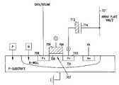
- FIG. 7illustrates a memory cell 700 according to the teachings of the present invention.
- memory cell 700includes a PMOS transistor 701 formed in an n-type well 731 .
- the PMOS transistor 701includes a first source/drain region 708 , and a second source/drain region 710 , where the first and the second source/drain region, 708 and 710 include source/drain regions having a large work function.
- a channelis 707 located between the first and the second source/drain regions, 708 and 710 .
- a gate 709opposes the channel 707 .
- the gateincludes a gate having a large work function.
- a gate insulator 706separates the gate from the channel 707 .
- the gate insulator 706is less than 20 Angstroms thick.
- the memory cell 700further includes a capacitor 703 coupled to the second source/drain region 710 wherein a first and a second plate of the capacitor, 712 and 714 includes first and second plates having a large work function.
- embodiments of the present inventioninclude first and the second p-type polysilicon polycrystalline semiconductor plates selected from the group consisting of p-doped silicon, p-doped germanium, p-doped silicon germanium compounds, p-doped silicon carbide, p-doped silicon oxycarbide compounds, p-doped gallium nitride compounds, and p-doped gallium aluminum nitride compounds.
- the first and the second plates 712 and 714include metal plates selected from the group consisting of cobalt, nickel, ruthenium, rhodium, palladium, iridium, platinum and gold.
- the first and the second plates 712 and 714include metallic nitride plates selected from the group consisting of titanium nitride, tantalum nitride, tungsten nitride, and molybdenum nitride.
- embodiments of the present inventioninclude a gate 709 that includes a metal gate 709 selected from the group consisting of cobalt, nickel, ruthenium, rhodium, palladium, iridium, platinum and gold.
- the gate 709includes a metallic nitride gate 709 selected from the group consisting of titanium nitride, tantalum nitride, tungsten nitride, and molybdenum nitride.
- the gate 709includes a p-type polycrystalline semiconductor gate selected from the group consisting of p-doped silicon, p-doped germanium, p-doped silicon germanium compounds, p-doped silicon carbide, p-doped silicon oxycarbide compounds, p-doped gallium nitride compounds, and p-doped gallium aluminum nitride compounds.
- the n-type well 731is tied to a positive voltage which is less than a power supply voltage. In an alternative embodiment of FIG. 7 , the n-type well 731 is tied to a voltage which is equal to a power supply voltage. In still another embodiment of the present invention, the n-type well 731 is tied to a voltage which is greater than a power supply voltage.
- an array plate voltage of Vcc/2serves to reduce the electric field across the capacitor dielectric to reduce dielectric leakage currents, like tunneling and reduce the probability of dielectric breakdown.
- the array platemight be tied to Vcc and the large work function of the other individual capacitor plate used to reduce the tunneling leakage currents since there would either be no electric field or voltage across the dielectric when a 1 was stored in the capacitor or only a negative potential of magnitude Vcc when a zero is stored in the capacitor. If only a negative potential difference is used then the large work function plate material will reduce the tunneling leakage current.
- both the array plate and capacitor plateare made of the same large work function material then an array plate potential of Vcc/2 can be used since either plate will have a large work function and it will be difficult to cause electron tunneling from either. If the array plate is not of the same material and is not a high work function material then an intermediate value of array plate potential other than Vcc/2 might be an optimum choice.
- the disclosureis not so limited. For purposes of illustration we will assume the plates are of the same material and the array plate is at a potential of Vcc/2. By using capacitor plate materials with large work functions, as shown in FIGS. 6 and 7 , the tunneling leakage currents of the storage capacitors can be eliminated.
- the P+ source/drain regioncan be formed of any of the semiconductor materials described herein having a large work function.
- Tunneling leakage from the gatecan be avoided or eliminated by using gate materials with a large work function. These tunneling currents can also be reduced by biasing the n-well at a more negative potential or less than the power supply voltage Vdd; however, this can result in extra transistor subthreshold leakage since the source to n-well will be forward biased. Biasing the n-well to a potential less than Vdd will however result in less source/drain junction leakage when a zero is stored in the cell since the reverse bias between the source/drain and well will be smaller. Biasing the n-well more positive or above Vdd will result in less junction leakage tending to reduce the cell capacitor plate to voltages below Vdd when a one is stored on the capacitor plate. A variety of well potentials can thus be employed to meet different application requirements and the disclosure is not so limited by any particular n-well potential.
- a first methodincludes a method of forming a memory cell.
- This methodincludes forming a PMOS transistor an n-type well.
- Forming the PMOS transistorincludes forming a first and a second source/drain regions separated by a channel.
- Forming the first and the second source/drain regionsincludes forming source/drain regions having a large work function.
- the methodfurther includes forming a gate opposing the channel.
- forming the gateincludes forming a gate having a work function of greater than 4.1 eV.
- a gate insulatoris formed separating the gate from the channel. In one embodiment, the gate insulator is formed to a thickness of less than 20 Angstroms.
- the methodincludes forming a storage device coupled to the second source/drain region. Forming the storage device includes forming a storage device having a first and a second storage node separated by a dielectric. According to the teachings of the present invention at least one of the first and the second storage nodes has a large work function. In one embodiment, the at least one storage node having a large work function includes a work function greater than 4.1 eV.
- forming the PMOS transistor in an n-type wellincludes coupling the n-type well to a positive voltage which is less than a power supply voltage. In another embodiment of the above method forming the PMOS transistor in an n-type well includes coupling the n-type well to a voltage which is equal to a power supply voltage. In yet another embodiment of the above method forming the PMOS transistor in an n-type well includes coupling the n-type well to a voltage which is greater than a power supply voltage.
- forming the first and the second storage nodesincludes forming the first and the second storage nodes of the same material.
- forming the first and the second source/drain regions having a large work functionincludes forming the first and the second source/drain regions with a work function greater than 4.1 eV.
- forming the first and the second storage nodesincludes forming first and second storage nodes which include a p-type polysilicon polycrystalline semiconductor material selected from the group consisting of p-doped silicon, p-doped germanium, p-doped silicon germanium compounds, p-doped silicon carbide, p-doped silicon oxycarbide compounds, p-doped gallium nitride compounds, and p-doped gallium aluminum nitride compounds.
- a p-type polysilicon polycrystalline semiconductor materialselected from the group consisting of p-doped silicon, p-doped germanium, p-doped silicon germanium compounds, p-doped silicon carbide, p-doped silicon oxycarbide compounds, p-doped gallium nitride compounds, and p-doped gallium aluminum nitride compounds.
- forming the first and the second storage nodesincludes forming the first and the second storage nodes of a metal selected from the group consisting of cobalt, nickel, ruthenium, rhodium, palladium, iridium, platinum and gold.
- forming the first and the second storage nodesincludes forming the first and the second storage nodes of a metallic nitride selected from the group consisting of titanium nitride, tantalum nitride, tungsten nitride, and molybdenum nitride.
- forming the gateincludes forming a metal gate selected from the group consisting of cobalt, nickel, ruthenium, rhodium, palladium, iridium, platinum and gold.
- forming the gateincludes forming a metallic nitride gate selected from the group consisting of titanium nitride, tantalum nitride, tungsten nitride, and molybdenum nitride.
- forming the gateincludes forming a p-type polycrystalline semiconductor gate selected from the group consisting of p-doped silicon, p-doped germanium, p-doped silicon germanium compounds, p-doped silicon carbide, p-doped silicon oxycarbide compounds, p-doped gallium nitride compounds, and p-doped gallium aluminum nitride compounds.
- Another method embodiment of the present inventionincludes a method for operating a memory cell.
- This methodincludes applying a negative voltage to a gate of a PMOS transistor formed in an n-type well.
- the PMOS transistorincludes a first source/drain region and a second source/drain region.
- the first and the second source/drain regioninclude source/drain regions having a large work function.
- a channelis located between the first and the second source/drain regions.
- a gateopposes the channel.
- the gateincludes a gate having a large work function.
- a gate insulatorseparates the gate from the channel. In one embodiment, the gate insulator is less than 20 Angstroms thick.
- the methodfurther includes coupling the n-type well to a positive voltage which is less than a power supply voltage.
- the methodfurther includes reading a charge level of a storage device.
- the storage deviceincludes a first and a second storage node. At least one of the first and the second storage nodes is formed of a material having a large work function.
- coupling the n-type well to a positive voltage which is less than a power supply voltageachieves lower tunneling charge leakage from the gate.
- Another method embodiment for the present inventionincludes a method for operating a memory cell.
- This methodincludes applying a negative voltage to a gate of a PMOS transistor formed in an n-type well.
- the PMOS transistorincludes a first source/drain region and a second source/drain region.
- the first and the second source/drain regioninclude source/drain regions having a large work function.
- a gateopposes the channel.
- the gateincludes a gate having a large work function.
- a gate insulatorseparates the gate from the channel.
- the gate insulatoris less than 20 Angstroms thick.
- the methodfurther includes coupling the n-type well to a voltage which is equal to a power supply voltage.
- the methodincludes reading a charge level of a storage device.
- the storage deviceincludes a first and a second storage node.
- at least one of the first and the second storage nodesincludes a storage node formed of a material having a large work function.
- coupling the n-type well to a voltage which is equal to a power supply voltageachieves lower tunneling charge leakage from the gate and lower junction leakage from the second source/drain region and storage device when the storage device is not charged.
- Another method embodiment of the present inventionincludes a method for operating a memory cell.
- This embodimentincludes applying a negative voltage to a gate of a PMOS transistor formed in an n-type well.
- the PMOS transistorincludes a first source/drain region and a second source/drain region.
- the first and the second source/drain regioninclude source/drain regions formed of a material having a large work function.
- a channelis located between the first and the second source/drain regions and a gate opposes the channel.
- the gateincludes a gate having a large work function.
- a gate insulatorseparates the gate from the channel. In one embodiment, the gate insulator is less than 20 Angstroms thick.
- the methodfurther includes coupling the n-type well to a voltage which is greater than a power supply voltage.
- the methodfurther includes reading a charge level of a storage device.
- the storage deviceincludes a first and a second storage node.
- the first and the second storage nodesincludes at least one storage node formed of a material having a large work function.
Landscapes
- Engineering & Computer Science (AREA)
- Manufacturing & Machinery (AREA)
- Microelectronics & Electronic Packaging (AREA)
- Computer Hardware Design (AREA)
- Semiconductor Memories (AREA)
Abstract
Description
Claims (43)
Priority Applications (2)
| Application Number | Priority Date | Filing Date | Title |
|---|---|---|---|
| US11/267,009US7235837B2 (en) | 2001-08-30 | 2005-11-04 | Technique to control tunneling currents in DRAM capacitors, cells, and devices |
| US11/759,727US20070228438A1 (en) | 2001-08-30 | 2007-06-07 | Technique to control tunneling currents in dram capacitors, cells, and devices |
Applications Claiming Priority (3)
| Application Number | Priority Date | Filing Date | Title |
|---|---|---|---|
| US09/945,310US6664589B2 (en) | 2001-08-30 | 2001-08-30 | Technique to control tunneling currents in DRAM capacitors, cells, and devices |
| US10/721,585US6979607B2 (en) | 2001-08-30 | 2003-11-25 | Technique to control tunneling currents in DRAM capacitors, cells, and devices |
| US11/267,009US7235837B2 (en) | 2001-08-30 | 2005-11-04 | Technique to control tunneling currents in DRAM capacitors, cells, and devices |
Related Parent Applications (1)
| Application Number | Title | Priority Date | Filing Date |
|---|---|---|---|
| US10/721,585ContinuationUS6979607B2 (en) | 2001-08-30 | 2003-11-25 | Technique to control tunneling currents in DRAM capacitors, cells, and devices |
Related Child Applications (1)
| Application Number | Title | Priority Date | Filing Date |
|---|---|---|---|
| US11/759,727ContinuationUS20070228438A1 (en) | 2001-08-30 | 2007-06-07 | Technique to control tunneling currents in dram capacitors, cells, and devices |
Publications (2)
| Publication Number | Publication Date |
|---|---|
| US20060054956A1 US20060054956A1 (en) | 2006-03-16 |
| US7235837B2true US7235837B2 (en) | 2007-06-26 |
Family
ID=25482949
Family Applications (4)
| Application Number | Title | Priority Date | Filing Date |
|---|---|---|---|
| US09/945,310Expired - LifetimeUS6664589B2 (en) | 2001-08-30 | 2001-08-30 | Technique to control tunneling currents in DRAM capacitors, cells, and devices |
| US10/721,585Expired - Fee RelatedUS6979607B2 (en) | 2001-08-30 | 2003-11-25 | Technique to control tunneling currents in DRAM capacitors, cells, and devices |
| US11/267,009Expired - LifetimeUS7235837B2 (en) | 2001-08-30 | 2005-11-04 | Technique to control tunneling currents in DRAM capacitors, cells, and devices |
| US11/759,727AbandonedUS20070228438A1 (en) | 2001-08-30 | 2007-06-07 | Technique to control tunneling currents in dram capacitors, cells, and devices |
Family Applications Before (2)
| Application Number | Title | Priority Date | Filing Date |
|---|---|---|---|
| US09/945,310Expired - LifetimeUS6664589B2 (en) | 2001-08-30 | 2001-08-30 | Technique to control tunneling currents in DRAM capacitors, cells, and devices |
| US10/721,585Expired - Fee RelatedUS6979607B2 (en) | 2001-08-30 | 2003-11-25 | Technique to control tunneling currents in DRAM capacitors, cells, and devices |
Family Applications After (1)
| Application Number | Title | Priority Date | Filing Date |
|---|---|---|---|
| US11/759,727AbandonedUS20070228438A1 (en) | 2001-08-30 | 2007-06-07 | Technique to control tunneling currents in dram capacitors, cells, and devices |
Country Status (1)
| Country | Link |
|---|---|
| US (4) | US6664589B2 (en) |
Families Citing this family (83)
| Publication number | Priority date | Publication date | Assignee | Title |
|---|---|---|---|---|
| US6664589B2 (en)* | 2001-08-30 | 2003-12-16 | Micron Technology, Inc. | Technique to control tunneling currents in DRAM capacitors, cells, and devices |
| US7180123B2 (en)* | 2003-07-21 | 2007-02-20 | Macronix International Co., Ltd. | Method for programming programmable eraseless memory |
| US7132350B2 (en) | 2003-07-21 | 2006-11-07 | Macronix International Co., Ltd. | Method for manufacturing a programmable eraseless memory |
| US20050035429A1 (en)* | 2003-08-15 | 2005-02-17 | Yeh Chih Chieh | Programmable eraseless memory |
| US7064050B2 (en)* | 2003-11-28 | 2006-06-20 | International Business Machines Corporation | Metal carbide gate structure and method of fabrication |
| US7144775B2 (en)* | 2004-05-18 | 2006-12-05 | Atmel Corporation | Low-voltage single-layer polysilicon eeprom memory cell |
| US7091075B2 (en)* | 2004-07-09 | 2006-08-15 | Atmel Corporation | Fabrication of an EEPROM cell with SiGe source/drain regions |
| US7011980B1 (en) | 2005-05-09 | 2006-03-14 | International Business Machines Corporation | Method and structures for measuring gate tunneling leakage parameters of field effect transistors |
| US7279740B2 (en) | 2005-05-12 | 2007-10-09 | Micron Technology, Inc. | Band-engineered multi-gated non-volatile memory device with enhanced attributes |
| US7402850B2 (en)* | 2005-06-21 | 2008-07-22 | Micron Technology, Inc. | Back-side trapped non-volatile memory device |
| US7829938B2 (en)* | 2005-07-14 | 2010-11-09 | Micron Technology, Inc. | High density NAND non-volatile memory device |
| US7629641B2 (en)* | 2005-08-31 | 2009-12-08 | Micron Technology, Inc. | Band engineered nano-crystal non-volatile memory device utilizing enhanced gate injection |
| US7446372B2 (en)* | 2005-09-01 | 2008-11-04 | Micron Technology, Inc. | DRAM tunneling access transistor |
| US7429767B2 (en)* | 2005-09-01 | 2008-09-30 | Micron Technology, Inc. | High performance multi-level non-volatile memory device |
| US7606066B2 (en) | 2005-09-07 | 2009-10-20 | Innovative Silicon Isi Sa | Memory cell and memory cell array having an electrically floating body transistor, and methods of operating same |
| US7492632B2 (en) | 2006-04-07 | 2009-02-17 | Innovative Silicon Isi Sa | Memory array having a programmable word length, and method of operating same |
| US8648403B2 (en)* | 2006-04-21 | 2014-02-11 | International Business Machines Corporation | Dynamic memory cell structures |
| US7933142B2 (en)* | 2006-05-02 | 2011-04-26 | Micron Technology, Inc. | Semiconductor memory cell and array using punch-through to program and read same |
| US8069377B2 (en)* | 2006-06-26 | 2011-11-29 | Micron Technology, Inc. | Integrated circuit having memory array including ECC and column redundancy and method of operating the same |
| US7542340B2 (en)* | 2006-07-11 | 2009-06-02 | Innovative Silicon Isi Sa | Integrated circuit including memory array having a segmented bit line architecture and method of controlling and/or operating same |
| US7466617B2 (en)* | 2007-01-16 | 2008-12-16 | International Business Machines Corporation | Multi-port dynamic memory structures |
| KR101277402B1 (en) | 2007-01-26 | 2013-06-20 | 마이크론 테크놀로지, 인코포레이티드 | Floating-body dram transistor comprising source/drain regions separated from the gated body region |
| US8518774B2 (en)* | 2007-03-29 | 2013-08-27 | Micron Technology, Inc. | Manufacturing process for zero-capacitor random access memory circuits |
| US8064274B2 (en)* | 2007-05-30 | 2011-11-22 | Micron Technology, Inc. | Integrated circuit having voltage generation circuitry for memory cell array, and method of operating and/or controlling same |
| US8085594B2 (en)* | 2007-06-01 | 2011-12-27 | Micron Technology, Inc. | Reading technique for memory cell with electrically floating body transistor |
| WO2009039169A1 (en) | 2007-09-17 | 2009-03-26 | Innovative Silicon S.A. | Refreshing data of memory cells with electrically floating body transistors |
| US8536628B2 (en) | 2007-11-29 | 2013-09-17 | Micron Technology, Inc. | Integrated circuit having memory cell array including barriers, and method of manufacturing same |
| US8349662B2 (en)* | 2007-12-11 | 2013-01-08 | Micron Technology, Inc. | Integrated circuit having memory cell array, and method of manufacturing same |
| US8773933B2 (en) | 2012-03-16 | 2014-07-08 | Micron Technology, Inc. | Techniques for accessing memory cells |
| US8014195B2 (en) | 2008-02-06 | 2011-09-06 | Micron Technology, Inc. | Single transistor memory cell |
| US8189376B2 (en)* | 2008-02-08 | 2012-05-29 | Micron Technology, Inc. | Integrated circuit having memory cells including gate material having high work function, and method of manufacturing same |
| US7957206B2 (en) | 2008-04-04 | 2011-06-07 | Micron Technology, Inc. | Read circuitry for an integrated circuit having memory cells and/or a memory cell array, and method of operating same |
| US7947543B2 (en)* | 2008-09-25 | 2011-05-24 | Micron Technology, Inc. | Recessed gate silicon-on-insulator floating body device with self-aligned lateral isolation |
| US7933140B2 (en) | 2008-10-02 | 2011-04-26 | Micron Technology, Inc. | Techniques for reducing a voltage swing |
| US7924630B2 (en)* | 2008-10-15 | 2011-04-12 | Micron Technology, Inc. | Techniques for simultaneously driving a plurality of source lines |
| US8223574B2 (en)* | 2008-11-05 | 2012-07-17 | Micron Technology, Inc. | Techniques for block refreshing a semiconductor memory device |
| US8213226B2 (en) | 2008-12-05 | 2012-07-03 | Micron Technology, Inc. | Vertical transistor memory cell and array |
| US8319294B2 (en)* | 2009-02-18 | 2012-11-27 | Micron Technology, Inc. | Techniques for providing a source line plane |
| WO2010102106A2 (en)* | 2009-03-04 | 2010-09-10 | Innovative Silicon Isi Sa | Techniques for forming a contact to a buried diffusion layer in a semiconductor memory device |
| US8748959B2 (en)* | 2009-03-31 | 2014-06-10 | Micron Technology, Inc. | Semiconductor memory device |
| US8139418B2 (en)* | 2009-04-27 | 2012-03-20 | Micron Technology, Inc. | Techniques for controlling a direct injection semiconductor memory device |
| US8508994B2 (en) | 2009-04-30 | 2013-08-13 | Micron Technology, Inc. | Semiconductor device with floating gate and electrically floating body |
| US8498157B2 (en)* | 2009-05-22 | 2013-07-30 | Micron Technology, Inc. | Techniques for providing a direct injection semiconductor memory device |
| US8537610B2 (en)* | 2009-07-10 | 2013-09-17 | Micron Technology, Inc. | Techniques for providing a semiconductor memory device |
| US9076543B2 (en) | 2009-07-27 | 2015-07-07 | Micron Technology, Inc. | Techniques for providing a direct injection semiconductor memory device |
| US8199595B2 (en)* | 2009-09-04 | 2012-06-12 | Micron Technology, Inc. | Techniques for sensing a semiconductor memory device |
| US9012766B2 (en) | 2009-11-12 | 2015-04-21 | Silevo, Inc. | Aluminum grid as backside conductor on epitaxial silicon thin film solar cells |
| US8174881B2 (en) | 2009-11-24 | 2012-05-08 | Micron Technology, Inc. | Techniques for reducing disturbance in a semiconductor device |
| US8310893B2 (en)* | 2009-12-16 | 2012-11-13 | Micron Technology, Inc. | Techniques for reducing impact of array disturbs in a semiconductor memory device |
| US8416636B2 (en)* | 2010-02-12 | 2013-04-09 | Micron Technology, Inc. | Techniques for controlling a semiconductor memory device |
| US8576631B2 (en)* | 2010-03-04 | 2013-11-05 | Micron Technology, Inc. | Techniques for sensing a semiconductor memory device |
| US8411513B2 (en)* | 2010-03-04 | 2013-04-02 | Micron Technology, Inc. | Techniques for providing a semiconductor memory device having hierarchical bit lines |
| US8369177B2 (en)* | 2010-03-05 | 2013-02-05 | Micron Technology, Inc. | Techniques for reading from and/or writing to a semiconductor memory device |
| US8547738B2 (en) | 2010-03-15 | 2013-10-01 | Micron Technology, Inc. | Techniques for providing a semiconductor memory device |
| US8686283B2 (en)* | 2010-05-04 | 2014-04-01 | Silevo, Inc. | Solar cell with oxide tunneling junctions |
| US20120318340A1 (en)* | 2010-05-04 | 2012-12-20 | Silevo, Inc. | Back junction solar cell with tunnel oxide |
| US8411524B2 (en) | 2010-05-06 | 2013-04-02 | Micron Technology, Inc. | Techniques for refreshing a semiconductor memory device |
| US9214576B2 (en) | 2010-06-09 | 2015-12-15 | Solarcity Corporation | Transparent conducting oxide for photovoltaic devices |
| US9773928B2 (en) | 2010-09-10 | 2017-09-26 | Tesla, Inc. | Solar cell with electroplated metal grid |
| US9800053B2 (en) | 2010-10-08 | 2017-10-24 | Tesla, Inc. | Solar panels with integrated cell-level MPPT devices |
| US8531878B2 (en) | 2011-05-17 | 2013-09-10 | Micron Technology, Inc. | Techniques for providing a semiconductor memory device |
| US9054256B2 (en) | 2011-06-02 | 2015-06-09 | Solarcity Corporation | Tunneling-junction solar cell with copper grid for concentrated photovoltaic application |
| US9559216B2 (en) | 2011-06-06 | 2017-01-31 | Micron Technology, Inc. | Semiconductor memory device and method for biasing same |
| US8679905B2 (en)* | 2011-06-08 | 2014-03-25 | Cbrite Inc. | Metal oxide TFT with improved source/drain contacts |
| US9412623B2 (en)* | 2011-06-08 | 2016-08-09 | Cbrite Inc. | Metal oxide TFT with improved source/drain contacts and reliability |
| JP6351601B2 (en) | 2012-10-04 | 2018-07-04 | ソーラーシティ コーポレーション | Photovoltaic device using electroplated metal grid |
| US9865754B2 (en) | 2012-10-10 | 2018-01-09 | Tesla, Inc. | Hole collectors for silicon photovoltaic cells |
| US9281436B2 (en) | 2012-12-28 | 2016-03-08 | Solarcity Corporation | Radio-frequency sputtering system with rotary target for fabricating solar cells |
| US10074755B2 (en) | 2013-01-11 | 2018-09-11 | Tesla, Inc. | High efficiency solar panel |
| US9219174B2 (en) | 2013-01-11 | 2015-12-22 | Solarcity Corporation | Module fabrication of solar cells with low resistivity electrodes |
| US9412884B2 (en) | 2013-01-11 | 2016-08-09 | Solarcity Corporation | Module fabrication of solar cells with low resistivity electrodes |
| US9624595B2 (en) | 2013-05-24 | 2017-04-18 | Solarcity Corporation | Electroplating apparatus with improved throughput |
| US10309012B2 (en) | 2014-07-03 | 2019-06-04 | Tesla, Inc. | Wafer carrier for reducing contamination from carbon particles and outgassing |
| KR102235613B1 (en)* | 2014-11-20 | 2021-04-02 | 삼성전자주식회사 | Semiconductor device having metal oxide semiconductor capacitor |
| US9899546B2 (en) | 2014-12-05 | 2018-02-20 | Tesla, Inc. | Photovoltaic cells with electrodes adapted to house conductive paste |
| US9947822B2 (en) | 2015-02-02 | 2018-04-17 | Tesla, Inc. | Bifacial photovoltaic module using heterojunction solar cells |
| US9761744B2 (en) | 2015-10-22 | 2017-09-12 | Tesla, Inc. | System and method for manufacturing photovoltaic structures with a metal seed layer |
| US9842956B2 (en) | 2015-12-21 | 2017-12-12 | Tesla, Inc. | System and method for mass-production of high-efficiency photovoltaic structures |
| US9496429B1 (en) | 2015-12-30 | 2016-11-15 | Solarcity Corporation | System and method for tin plating metal electrodes |
| US10115838B2 (en) | 2016-04-19 | 2018-10-30 | Tesla, Inc. | Photovoltaic structures with interlocking busbars |
| US10672919B2 (en) | 2017-09-19 | 2020-06-02 | Tesla, Inc. | Moisture-resistant solar cells for solar roof tiles |
| US11190128B2 (en) | 2018-02-27 | 2021-11-30 | Tesla, Inc. | Parallel-connected solar roof tile modules |
| CN111555428B (en)* | 2020-06-05 | 2023-03-03 | 电子科技大学 | A charging and discharging and energy management circuit for micro energy harvesting system |
Citations (29)
| Publication number | Priority date | Publication date | Assignee | Title |
|---|---|---|---|---|
| US3387286A (en) | 1967-07-14 | 1968-06-04 | Ibm | Field-effect transistor memory |
| US5408115A (en) | 1994-04-04 | 1995-04-18 | Motorola Inc. | Self-aligned, split-gate EEPROM device |
| US5530581A (en) | 1995-05-31 | 1996-06-25 | Eic Laboratories, Inc. | Protective overlayer material and electro-optical coating using same |
| US5852311A (en) | 1996-06-07 | 1998-12-22 | Samsung Electronics Co., Ltd. | Non-volatile memory devices including capping layer contact holes |
| US5869370A (en) | 1997-12-29 | 1999-02-09 | Taiwan Semiconductor Manufacturing Company Ltd. | Ultra thin tunneling oxide using buffer CVD to improve edge thinning |
| US5886368A (en) | 1997-07-29 | 1999-03-23 | Micron Technology, Inc. | Transistor with silicon oxycarbide gate and methods of fabrication and use |
| US5989958A (en) | 1997-01-29 | 1999-11-23 | Micron Technology, Inc. | Flash memory with microcrystalline silicon carbide film floating gate |
| US6031263A (en) | 1997-07-29 | 2000-02-29 | Micron Technology, Inc. | DEAPROM and transistor with gallium nitride or gallium aluminum nitride gate |
| US6246089B1 (en) | 1997-04-14 | 2001-06-12 | Taiwan Semiconductor Manufacturing Company | P-channel EEPROM devices |
| US6245613B1 (en) | 1998-04-28 | 2001-06-12 | International Business Machines Corporation | Field effect transistor having a floating gate |
| US6249460B1 (en) | 2000-02-28 | 2001-06-19 | Micron Technology, Inc. | Dynamic flash memory cells with ultrathin tunnel oxides |
| US6265266B1 (en) | 1996-09-27 | 2001-07-24 | Xilinx, Inc. | Method of forming a two transistor flash EPROM cell |
| US6278155B1 (en) | 1996-04-26 | 2001-08-21 | Denso Corporation | P-channel MOSFET semiconductor device having a low on resistance |
| US6294420B1 (en)* | 1997-01-31 | 2001-09-25 | Texas Instruments Incorporated | Integrated circuit capacitor |
| US6316316B1 (en) | 1998-03-06 | 2001-11-13 | Texas Instruments-Acer Incorporated | Method of forming high density and low power flash memories with a high capacitive-coupling ratio |
| US20020016081A1 (en) | 1999-02-04 | 2002-02-07 | Tower Semiconductor Ltd. | Methods for fabricating a semiconductor chip having CMOS devices and fieldless array |
| US6351428B2 (en) | 2000-02-29 | 2002-02-26 | Micron Technology, Inc. | Programmable low voltage decode circuits with ultra-thin tunnel oxides |
| US6376302B1 (en)* | 1998-12-24 | 2002-04-23 | Agere Systems Guardian Corp. | Method for forming a DRAM capacitor having a high dielectric constant dielectric and capacitor made thereby |
| US6383939B1 (en) | 1998-07-17 | 2002-05-07 | Advanced Micro Devices, Inc. | Method for etching memory gate stack using thin resist layer |
| US6384448B1 (en) | 2000-02-28 | 2002-05-07 | Micron Technology, Inc. | P-channel dynamic flash memory cells with ultrathin tunnel oxides |
| US6411160B1 (en) | 1998-08-27 | 2002-06-25 | Hitachi, Ltd. | Semiconductor integrated circuit device |
| US6441423B1 (en)* | 2000-05-31 | 2002-08-27 | International Business Machines Corporation | Trench capacitor with an intrinsically balanced field across the dielectric |
| US20030001197A1 (en) | 1999-10-08 | 2003-01-02 | Macronix International Co., Ltd. | Method for forming a flash memory cell having contoured floating gate surface |
| US20030011009A1 (en) | 2001-06-18 | 2003-01-16 | Motorola, Inc. | Grooved channel schottky mosfet |
| US6515328B1 (en) | 1999-02-04 | 2003-02-04 | Advanced Micro Devices, Inc. | Semiconductor devices with reduced control gate dimensions |
| US6583011B1 (en) | 2000-01-11 | 2003-06-24 | Chartered Semiconductor Manufacturing Ltd. | Method for forming damascene dual gate for improved oxide uniformity and control |
| US6639835B2 (en) | 2000-02-29 | 2003-10-28 | Micron Technology, Inc. | Static NVRAM with ultra thin tunnel oxides |
| US20030201491A1 (en) | 1998-12-17 | 2003-10-30 | Samsung Electronics Co., Ltd. | Semiconductor device containing oxide/nitride/oxide dielectric layer and method of forming the same |
| US6664589B2 (en)* | 2001-08-30 | 2003-12-16 | Micron Technology, Inc. | Technique to control tunneling currents in DRAM capacitors, cells, and devices |
- 2001
- 2001-08-30USUS09/945,310patent/US6664589B2/ennot_activeExpired - Lifetime
- 2003
- 2003-11-25USUS10/721,585patent/US6979607B2/ennot_activeExpired - Fee Related
- 2005
- 2005-11-04USUS11/267,009patent/US7235837B2/ennot_activeExpired - Lifetime
- 2007
- 2007-06-07USUS11/759,727patent/US20070228438A1/ennot_activeAbandoned
Patent Citations (31)
| Publication number | Priority date | Publication date | Assignee | Title |
|---|---|---|---|---|
| US3387286A (en) | 1967-07-14 | 1968-06-04 | Ibm | Field-effect transistor memory |
| US5408115A (en) | 1994-04-04 | 1995-04-18 | Motorola Inc. | Self-aligned, split-gate EEPROM device |
| US5530581A (en) | 1995-05-31 | 1996-06-25 | Eic Laboratories, Inc. | Protective overlayer material and electro-optical coating using same |
| US6278155B1 (en) | 1996-04-26 | 2001-08-21 | Denso Corporation | P-channel MOSFET semiconductor device having a low on resistance |
| US5852311A (en) | 1996-06-07 | 1998-12-22 | Samsung Electronics Co., Ltd. | Non-volatile memory devices including capping layer contact holes |
| US6265266B1 (en) | 1996-09-27 | 2001-07-24 | Xilinx, Inc. | Method of forming a two transistor flash EPROM cell |
| US5989958A (en) | 1997-01-29 | 1999-11-23 | Micron Technology, Inc. | Flash memory with microcrystalline silicon carbide film floating gate |
| US6294420B1 (en)* | 1997-01-31 | 2001-09-25 | Texas Instruments Incorporated | Integrated circuit capacitor |
| US6246089B1 (en) | 1997-04-14 | 2001-06-12 | Taiwan Semiconductor Manufacturing Company | P-channel EEPROM devices |
| US5886368A (en) | 1997-07-29 | 1999-03-23 | Micron Technology, Inc. | Transistor with silicon oxycarbide gate and methods of fabrication and use |
| US6031263A (en) | 1997-07-29 | 2000-02-29 | Micron Technology, Inc. | DEAPROM and transistor with gallium nitride or gallium aluminum nitride gate |
| US5869370A (en) | 1997-12-29 | 1999-02-09 | Taiwan Semiconductor Manufacturing Company Ltd. | Ultra thin tunneling oxide using buffer CVD to improve edge thinning |
| US6316316B1 (en) | 1998-03-06 | 2001-11-13 | Texas Instruments-Acer Incorporated | Method of forming high density and low power flash memories with a high capacitive-coupling ratio |
| US6245613B1 (en) | 1998-04-28 | 2001-06-12 | International Business Machines Corporation | Field effect transistor having a floating gate |
| US6383939B1 (en) | 1998-07-17 | 2002-05-07 | Advanced Micro Devices, Inc. | Method for etching memory gate stack using thin resist layer |
| US6411160B1 (en) | 1998-08-27 | 2002-06-25 | Hitachi, Ltd. | Semiconductor integrated circuit device |
| US20030201491A1 (en) | 1998-12-17 | 2003-10-30 | Samsung Electronics Co., Ltd. | Semiconductor device containing oxide/nitride/oxide dielectric layer and method of forming the same |
| US6376302B1 (en)* | 1998-12-24 | 2002-04-23 | Agere Systems Guardian Corp. | Method for forming a DRAM capacitor having a high dielectric constant dielectric and capacitor made thereby |
| US6515328B1 (en) | 1999-02-04 | 2003-02-04 | Advanced Micro Devices, Inc. | Semiconductor devices with reduced control gate dimensions |
| US20020016081A1 (en) | 1999-02-04 | 2002-02-07 | Tower Semiconductor Ltd. | Methods for fabricating a semiconductor chip having CMOS devices and fieldless array |
| US20030001197A1 (en) | 1999-10-08 | 2003-01-02 | Macronix International Co., Ltd. | Method for forming a flash memory cell having contoured floating gate surface |
| US6583011B1 (en) | 2000-01-11 | 2003-06-24 | Chartered Semiconductor Manufacturing Ltd. | Method for forming damascene dual gate for improved oxide uniformity and control |
| US6384448B1 (en) | 2000-02-28 | 2002-05-07 | Micron Technology, Inc. | P-channel dynamic flash memory cells with ultrathin tunnel oxides |
| US6456535B2 (en) | 2000-02-28 | 2002-09-24 | Micron Technology, Inc. | Dynamic flash memory cells with ultra thin tunnel oxides |
| US6249460B1 (en) | 2000-02-28 | 2001-06-19 | Micron Technology, Inc. | Dynamic flash memory cells with ultrathin tunnel oxides |
| US6351428B2 (en) | 2000-02-29 | 2002-02-26 | Micron Technology, Inc. | Programmable low voltage decode circuits with ultra-thin tunnel oxides |
| US6639835B2 (en) | 2000-02-29 | 2003-10-28 | Micron Technology, Inc. | Static NVRAM with ultra thin tunnel oxides |
| US6730960B2 (en) | 2000-02-29 | 2004-05-04 | Micron Technology, Inc. | Static NVRAM with ultra thin tunnel oxides |
| US6441423B1 (en)* | 2000-05-31 | 2002-08-27 | International Business Machines Corporation | Trench capacitor with an intrinsically balanced field across the dielectric |
| US20030011009A1 (en) | 2001-06-18 | 2003-01-16 | Motorola, Inc. | Grooved channel schottky mosfet |
| US6664589B2 (en)* | 2001-08-30 | 2003-12-16 | Micron Technology, Inc. | Technique to control tunneling currents in DRAM capacitors, cells, and devices |
Non-Patent Citations (20)
| Title |
|---|
| "Silicon Monoxide", CERAC, inc.-Silicon Monoxide, SIO, (2000),pp. 1-4. |
| Al-Ani, S.K.J. , et al., "The Effect of Temperature of the Optical Absorption Edge of Amorphous Thin Films of Silicon Monoxide", Phys. Stat. Sol.(b) 123, (1984),653-658. |
| Al-Ani, S.K.J. , et al., "The optical absorption edge of amorphous thin films of silicon monoxide", Journal of Materials Science, 19, (1984), 1737-1748. |
| Chand, N. , et al., "Tunability of intrinsic stress SiO/sub x/dielectric films formed by molecular beam deposition", IEE, (1995),2 pages. |
| Chau, R. , et al., "30nm Physical Gate Length CMOS Tansistors with 1.0 ps n-MOS and 1.7 ps p-MOS Gate Delays", IEEE Int. Electron, Devices Meeting, San Francisco, (Dec. 2000),pp. 45-48. |
| Demichelis, F. , et al., "Doped amorphous and microcrystalline silicon carbide as wide band-gap material", Wide Band Gap Semiconducors Symposium, Mat. Res. Soc., Pittsburgh, PA, (1992), 1 page. |
| Eldridge, J. M., et al., "Oxidation of Plasma-Deposited a-SixC1-x: H films", J. Electrochem. Soc., vol. 137, No. 7, (Jul. 1990),pp. 2266-2271. |
| Furusawa, T. , et al., "Simple, Reliable Cu/low-k Interconnect Integration Using Mechanically-strong Low-k Dielectric Material: Silicon-oxycarbide", Proc. IEEE Int. Interconnect Technology Conf., (Jun. 2000),pp. 222-224. |
| Hirayama, M. , et al., "Low-Temperature Growth of High-Integrity Silicon Oxide Films by Oxygen Radical Generated in High-Density Krypton Plasma", IEEE, (1999),4 pages. |
| Ilyas, M. , et al., "The optical absorption edge of amorphous thin films of silicon monoxide and of silicon monoxide mixed with titanium monoxide", IEEE, (2001),1 page. |
| Kubaschewski, O. , et al., "Oxidation of Metals and Alloys", Butterworths, London, (1962),pp. 53-64. |
| Maiti, B. , et al., "Metal Gates for Advanced CMOS Technology", Proc, Microelectronic Device Technology III, Santa Clara, CA, 22-23 , Soc. of Photo-Optical Instrumentation Engineers, Bellingham WA,(Sep. 1999),pp. 46-57. |
| Renlund, G. M., "Silicon oxycarbide glasses: Part I. Preparation and chemistry", J. Mater, Res., (Dec. 1991),pp. 2716-2722. |
| Renlund, G. M., "Silicon oxycarbide glasses: Part II. Structure and properties", J. Mater. Res., vol. 6, No. 12,(Dec. 1991),pp. 2723-2734. |
| Robinson, G. , "Passivation hardens lasers for low-cost package", 3 pages. |
| Shi, Y. , et al., "Tunneling Leakage Current in Ultrathin (less than 4nm) Nitride/Oxide Stack Dielectrics", IEEE Electron Device Letters, 19(10), (Oct. 1998),pp. 388-390. |
| Skriver, H. L., et al., "Surface energy and work function of elemental metals", Physical Review B (Condensed Matter), vol. 46, No. 11, (Sep. 15, 1992), 1 page. |
| Strass, A. , et al., "Fabrication and Characterisation of thin low-temperature MBE-compatible silicon oxides of different stoichiometry", Thin Solid Films 349, (1999),pp. 135-146. |
| Sze, S. M., "Physics of Semiconductor Devices", New York, Wiley-Interscience, ISBN: 0471842907,(1969),402-407. |
| Sze, S. M., "Physics of Semiconductor Devices,", Wiley, (1981),pp. 251, 396. |
Also Published As
| Publication number | Publication date |
|---|---|
| US6664589B2 (en) | 2003-12-16 |
| US6979607B2 (en) | 2005-12-27 |
| US20030042516A1 (en) | 2003-03-06 |
| US20060054956A1 (en) | 2006-03-16 |
| US20070228438A1 (en) | 2007-10-04 |
| US20040106251A1 (en) | 2004-06-03 |
Similar Documents
| Publication | Publication Date | Title |
|---|---|---|
| US7235837B2 (en) | Technique to control tunneling currents in DRAM capacitors, cells, and devices | |
| US6703673B2 (en) | SOI DRAM having P-doped poly gate for a memory pass transistor | |
| US5466961A (en) | Semiconductor device and method of manufacturing the same | |
| US7099192B2 (en) | Nonvolatile flash memory and method of operating the same | |
| US7362609B2 (en) | Memory cell | |
| US6784048B2 (en) | Method of fabricating a DRAM cell having a thin dielectric access transistor and a thick dielectric storage | |
| EP0535681B1 (en) | Semiconductor body, its manufacturing method, and semiconductor device using the body | |
| US6744676B2 (en) | DRAM cell having a capacitor structure fabricated partially in a cavity and method for operating same | |
| US7009243B2 (en) | Semiconductor memory device | |
| US6628551B2 (en) | Reducing leakage current in memory cells | |
| US20040021166A1 (en) | Pseudo-nonvolatile direct-tunneling floating-gate device | |
| US6756692B2 (en) | Semiconductor storage device having high soft-error immunity | |
| US5959336A (en) | Decoder circuit with short channel depletion transistors | |
| US6964892B2 (en) | N-channel metal oxide semiconductor (NMOS) driver circuit and method of making same | |
| US8076707B1 (en) | Pseudo-nonvolatile direct-tunneling floating-gate device | |
| US6885068B2 (en) | Storage element and SRAM cell structures using vertical FETs controlled by adjacent junction bias through shallow trench isolation | |
| US6674105B2 (en) | Semiconductor memory device and method of forming the same | |
| US7123518B2 (en) | Memory device | |
| US6362056B1 (en) | Method of making alternative to dual gate oxide for MOSFETs | |
| US20030218218A1 (en) | SRAM cell with reduced standby leakage current and method for forming the same | |
| US6534812B1 (en) | Memory cell with stored charge on its gate and a resistance element having non-linear resistance elements | |
| Fazio | A high density high performance 180 nm generation Etox/sup TM/flash memory technology | |
| US6429093B1 (en) | Sidewall process for forming a low resistance source line | |
| KR20050010004A (en) | Schottky barrier cmos device and method | |
| Van Vonno et al. | A 256 K static random-access memory implemented in silicon-on-insulator technology |
Legal Events
| Date | Code | Title | Description |
|---|---|---|---|
| FEPP | Fee payment procedure | Free format text:PAYOR NUMBER ASSIGNED (ORIGINAL EVENT CODE: ASPN); ENTITY STATUS OF PATENT OWNER: LARGE ENTITY | |
| STCF | Information on status: patent grant | Free format text:PATENTED CASE | |
| CC | Certificate of correction | ||
| FPAY | Fee payment | Year of fee payment:4 | |
| FPAY | Fee payment | Year of fee payment:8 | |
| AS | Assignment | Owner name:U.S. BANK NATIONAL ASSOCIATION, AS COLLATERAL AGENT, CALIFORNIA Free format text:SECURITY INTEREST;ASSIGNOR:MICRON TECHNOLOGY, INC.;REEL/FRAME:038669/0001 Effective date:20160426 Owner name:U.S. BANK NATIONAL ASSOCIATION, AS COLLATERAL AGEN Free format text:SECURITY INTEREST;ASSIGNOR:MICRON TECHNOLOGY, INC.;REEL/FRAME:038669/0001 Effective date:20160426 | |
| AS | Assignment | Owner name:MORGAN STANLEY SENIOR FUNDING, INC., AS COLLATERAL AGENT, MARYLAND Free format text:PATENT SECURITY AGREEMENT;ASSIGNOR:MICRON TECHNOLOGY, INC.;REEL/FRAME:038954/0001 Effective date:20160426 Owner name:MORGAN STANLEY SENIOR FUNDING, INC., AS COLLATERAL Free format text:PATENT SECURITY AGREEMENT;ASSIGNOR:MICRON TECHNOLOGY, INC.;REEL/FRAME:038954/0001 Effective date:20160426 | |
| AS | Assignment | Owner name:U.S. BANK NATIONAL ASSOCIATION, AS COLLATERAL AGENT, CALIFORNIA Free format text:CORRECTIVE ASSIGNMENT TO CORRECT THE REPLACE ERRONEOUSLY FILED PATENT #7358718 WITH THE CORRECT PATENT #7358178 PREVIOUSLY RECORDED ON REEL 038669 FRAME 0001. ASSIGNOR(S) HEREBY CONFIRMS THE SECURITY INTEREST;ASSIGNOR:MICRON TECHNOLOGY, INC.;REEL/FRAME:043079/0001 Effective date:20160426 Owner name:U.S. BANK NATIONAL ASSOCIATION, AS COLLATERAL AGEN Free format text:CORRECTIVE ASSIGNMENT TO CORRECT THE REPLACE ERRONEOUSLY FILED PATENT #7358718 WITH THE CORRECT PATENT #7358178 PREVIOUSLY RECORDED ON REEL 038669 FRAME 0001. ASSIGNOR(S) HEREBY CONFIRMS THE SECURITY INTEREST;ASSIGNOR:MICRON TECHNOLOGY, INC.;REEL/FRAME:043079/0001 Effective date:20160426 | |
| AS | Assignment | Owner name:JPMORGAN CHASE BANK, N.A., AS COLLATERAL AGENT, ILLINOIS Free format text:SECURITY INTEREST;ASSIGNORS:MICRON TECHNOLOGY, INC.;MICRON SEMICONDUCTOR PRODUCTS, INC.;REEL/FRAME:047540/0001 Effective date:20180703 Owner name:JPMORGAN CHASE BANK, N.A., AS COLLATERAL AGENT, IL Free format text:SECURITY INTEREST;ASSIGNORS:MICRON TECHNOLOGY, INC.;MICRON SEMICONDUCTOR PRODUCTS, INC.;REEL/FRAME:047540/0001 Effective date:20180703 | |
| AS | Assignment | Owner name:MICRON TECHNOLOGY, INC., IDAHO Free format text:RELEASE BY SECURED PARTY;ASSIGNOR:U.S. BANK NATIONAL ASSOCIATION, AS COLLATERAL AGENT;REEL/FRAME:047243/0001 Effective date:20180629 | |
| MAFP | Maintenance fee payment | Free format text:PAYMENT OF MAINTENANCE FEE, 12TH YEAR, LARGE ENTITY (ORIGINAL EVENT CODE: M1553); ENTITY STATUS OF PATENT OWNER: LARGE ENTITY Year of fee payment:12 | |
| AS | Assignment | Owner name:MICRON TECHNOLOGY, INC., IDAHO Free format text:RELEASE BY SECURED PARTY;ASSIGNOR:MORGAN STANLEY SENIOR FUNDING, INC., AS COLLATERAL AGENT;REEL/FRAME:050937/0001 Effective date:20190731 | |
| AS | Assignment | Owner name:MICRON TECHNOLOGY, INC., IDAHO Free format text:RELEASE BY SECURED PARTY;ASSIGNOR:JPMORGAN CHASE BANK, N.A., AS COLLATERAL AGENT;REEL/FRAME:051028/0001 Effective date:20190731 Owner name:MICRON SEMICONDUCTOR PRODUCTS, INC., IDAHO Free format text:RELEASE BY SECURED PARTY;ASSIGNOR:JPMORGAN CHASE BANK, N.A., AS COLLATERAL AGENT;REEL/FRAME:051028/0001 Effective date:20190731 |