US7235457B2 - High permeability layered films to reduce noise in high speed interconnects - Google Patents
High permeability layered films to reduce noise in high speed interconnectsDownload PDFInfo
- Publication number
- US7235457B2 US7235457B2US10/099,217US9921702AUS7235457B2US 7235457 B2US7235457 B2US 7235457B2US 9921702 AUS9921702 AUS 9921702AUS 7235457 B2US7235457 B2US 7235457B2
- Authority
- US
- United States
- Prior art keywords
- forming
- lines
- layer
- electrically conductive
- insulating material
- Prior art date
- Legal status (The legal status is an assumption and is not a legal conclusion. Google has not performed a legal analysis and makes no representation as to the accuracy of the status listed.)
- Expired - Lifetime, expires
Links
Images


Classifications
- G—PHYSICS
- G11—INFORMATION STORAGE
- G11C—STATIC STORES
- G11C5/00—Details of stores covered by group G11C11/00
- G11C5/06—Arrangements for interconnecting storage elements electrically, e.g. by wiring
- G11C5/063—Voltage and signal distribution in integrated semi-conductor memory access lines, e.g. word-line, bit-line, cross-over resistance, propagation delay
- H—ELECTRICITY
- H01—ELECTRIC ELEMENTS
- H01L—SEMICONDUCTOR DEVICES NOT COVERED BY CLASS H10
- H01L23/00—Details of semiconductor or other solid state devices
- H01L23/52—Arrangements for conducting electric current within the device in operation from one component to another, i.e. interconnections, e.g. wires, lead frames
- H01L23/522—Arrangements for conducting electric current within the device in operation from one component to another, i.e. interconnections, e.g. wires, lead frames including external interconnections consisting of a multilayer structure of conductive and insulating layers inseparably formed on the semiconductor body
- H01L23/5222—Capacitive arrangements or effects of, or between wiring layers
- H01L23/5225—Shielding layers formed together with wiring layers
- H—ELECTRICITY
- H01—ELECTRIC ELEMENTS
- H01L—SEMICONDUCTOR DEVICES NOT COVERED BY CLASS H10
- H01L23/00—Details of semiconductor or other solid state devices
- H01L23/52—Arrangements for conducting electric current within the device in operation from one component to another, i.e. interconnections, e.g. wires, lead frames
- H01L23/522—Arrangements for conducting electric current within the device in operation from one component to another, i.e. interconnections, e.g. wires, lead frames including external interconnections consisting of a multilayer structure of conductive and insulating layers inseparably formed on the semiconductor body
- H01L23/532—Arrangements for conducting electric current within the device in operation from one component to another, i.e. interconnections, e.g. wires, lead frames including external interconnections consisting of a multilayer structure of conductive and insulating layers inseparably formed on the semiconductor body characterised by the materials
- H01L23/53204—Conductive materials
- H01L23/53209—Conductive materials based on metals, e.g. alloys, metal silicides
- H—ELECTRICITY
- H01—ELECTRIC ELEMENTS
- H01L—SEMICONDUCTOR DEVICES NOT COVERED BY CLASS H10
- H01L2223/00—Details relating to semiconductor or other solid state devices covered by the group H01L23/00
- H01L2223/58—Structural electrical arrangements for semiconductor devices not otherwise provided for
- H01L2223/64—Impedance arrangements
- H01L2223/66—High-frequency adaptations
- H01L2223/6605—High-frequency electrical connections
- H01L2223/6627—Waveguides, e.g. microstrip line, strip line, coplanar line
- H—ELECTRICITY
- H01—ELECTRIC ELEMENTS
- H01L—SEMICONDUCTOR DEVICES NOT COVERED BY CLASS H10
- H01L23/00—Details of semiconductor or other solid state devices
- H01L23/58—Structural electrical arrangements for semiconductor devices not otherwise provided for, e.g. in combination with batteries
- H01L23/64—Impedance arrangements
- H01L23/66—High-frequency adaptations
- H—ELECTRICITY
- H01—ELECTRIC ELEMENTS
- H01L—SEMICONDUCTOR DEVICES NOT COVERED BY CLASS H10
- H01L2924/00—Indexing scheme for arrangements or methods for connecting or disconnecting semiconductor or solid-state bodies as covered by H01L24/00
- H01L2924/0001—Technical content checked by a classifier
- H01L2924/0002—Not covered by any one of groups H01L24/00, H01L24/00 and H01L2224/00
- H—ELECTRICITY
- H01—ELECTRIC ELEMENTS
- H01L—SEMICONDUCTOR DEVICES NOT COVERED BY CLASS H10
- H01L2924/00—Indexing scheme for arrangements or methods for connecting or disconnecting semiconductor or solid-state bodies as covered by H01L24/00
- H01L2924/19—Details of hybrid assemblies other than the semiconductor or other solid state devices to be connected
- H01L2924/1901—Structure
- H01L2924/1903—Structure including wave guides
- H—ELECTRICITY
- H01—ELECTRIC ELEMENTS
- H01L—SEMICONDUCTOR DEVICES NOT COVERED BY CLASS H10
- H01L2924/00—Indexing scheme for arrangements or methods for connecting or disconnecting semiconductor or solid-state bodies as covered by H01L24/00
- H01L2924/30—Technical effects
- H01L2924/301—Electrical effects
- H01L2924/3011—Impedance
Definitions
- the present inventionrelates generally to integrated circuits. More particularly, it pertains to structure and methods for improved transmission line interconnections.
- the metal lines over insulators and ground planes, or metal lines buried in close proximity to dielectric insulators and used for integrated circuit interconnectsare in reality transmission lines or strip lines.
- the use of coaxial interconnection lines for interconnections through the substrate in CMOS integrated circuitscan also be termed transmission lines or strip lines.
- Interconnection lines on interposers or printed circuit boardscan also be described as transmission lines.
- Most commonly used coaxial lineshave an impedance of 50 ohms or 75 ohms, it is difficult to achieve larger values. In the past these effects have not received much consideration on the integrated circuits themselves since the propagation speed with oxide insulators is 15 cm/ns and switching speeds on integrated circuits of the size of a centimeter have been slower than 1/15 ns or 70 picoseconds.
- FIG. 1illustrates R-C limited, short high impedance interconnections with capacitive loads.
- the drivermay simply be a CMOS inverter as shown in FIG. 1 and the receiver a simple CMOS amplifier, differential amplifier, or comparator.
- the CMOS receiverpresents a high impedance termination or load to the interconnection line. This is problematic in that:
- the switching time response or signal delayis determined mainly by the ability of the driver to charge up the capacitance of the line and the load capacitance
- noise voltagesmay be induced on the signal transmission line due to capacitive coupling and large voltage swing switching on adjacent lines, the noise voltage can be a large fraction of the signal voltage.
- FIG. 1shows the commonly used signal interconnection in CMOS integrated circuits, where voltage signals are transmitted from one location to another.
- the interconnection linesare normally loaded with the capacitive input of the next CMOS stage and the large stray capacitance of the line itself.
- the response timeis normally slow due to the limited ability of the line drivers to supply the large currents needed to charge these capacitances over large voltage swings. These times are usually much larger than the signal transmission time down the line so a lumped circuit model can be used to find the signal delay, as shown in FIG. 1 .
- the voltage swing on one linecan induce a large voltage swing or noise voltage on the adjacent line as shown in FIG. 1 .
- the noise voltageis just determined by the capacitance ratios, or ratio of interwire capacitance, Cint, to the capacitance of the interconnection wire, C.
- the novel low input impedance CMOS circuitoffers the following advantages: (1) the signal delay depends only on the velocity of light on the line and is easily predictable and reproducible, eliminating or allowing for compensation for signal and/or clock skew, (2) there are no reflections at the receiving end of the line and this minimizes ringing, and (3) noise signals will be smaller due to weaker coupling between lines resulting in better signal to noise ratios, the noise current will only be a small fraction of the signal current.
- One embodiment of the inventionincludes a method for forming transmission lines in an integrated circuit.
- the methodincludes forming a first layer of electrically conductive material on a substrate.
- a first layer of insulating materialis formed on the first layer of the electrically conductive material.
- a pair of layered high permeability shielding linesare formed on the first layer of insulating material.
- the pair of layered high permeability shielding linesinclude layered permalloy and Ni 45 Fe 55 films.
- a transmission lineis formed on the first layer of insulating material and between and parallel with the pair of layered high permeability shielding lines.
- a second layer of insulating materialis formed on the transmission line and the pair of layered high permeability shielding lines.
- the methodincludes forming a second layer of electrically conductive material on the second layer of insulating material.
- FIG. 1shows the commonly used signal interconnection in CMOS integrated circuits, where voltage signals are transmitted from one location to another.
- FIG. 2illustrates one technique to minimize the interwire capacitance, Cint, by using an intermediate line at ground for shielding.
- FIG. 3Aillustrates signal transmission using correctly terminated transmission lines and current sense amplifiers, according to the teachings of the present invention.
- FIG. 3Billustrates two interconnection lines in close proximity and the interwire capacitance between these lines and the mutual inductance coupling between the lines.
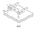
- FIG. 4is a perspective view illustrating a pair of neighboring transmission lines above a conductive substrate, according to the teachings of the present invention.
- FIG. 5is a schematic diagram for an interconnection on an integrated circuit according to the teachings of the present invention.
- FIG. 6illustrates one embodiment for a pair of neighboring transmission lines, according to the teachings of the present invention.
- FIG. 7illustrates another embodiment for a pair of neighboring transmission lines, according to the teachings of the present invention.
- FIG. 8illustrates another embodiment for a pair of neighboring transmission lines, according to the teachings of the present invention.
- FIG. 9illustrates another embodiment for a pair of neighboring transmission lines, according to the teachings of the present invention.
- FIG. 10illustrates another embodiment for a pair of neighboring transmission lines, according to the teachings of the present invention.
- FIG. 11illustrates another embodiment for a pair of neighboring transmission lines, according to the teachings of the present invention.
- FIG. 12illustrates another embodiment for a pair of neighboring transmission lines, according to the teachings of the present invention.
- FIG. 13is a block diagram which illustrates an embodiment of a system using line signaling according to teachings of the present invention.
- FIG. 14is a block diagram which illustrates another embodiment of a system according to teaching of the present invention.
- wafer and substrate used in the following descriptioninclude any structure having an exposed surface with which to form the integrated circuit (IC) structure of the invention.
- substrateis understood to include semiconductor wafers.
- substrateis also used to refer to semiconductor structures during processing, and may include other layers that have been fabricated thereupon. Both wafer and substrate include doped and undoped semiconductors, epitaxial semiconductor layers supported by a base semiconductor or insulator, as well as other semiconductor structures well known to one skilled in the art.
- conductoris understood to include semiconductors
- insulatoris defined to include any material that is less electrically conductive than the materials referred to as conductors.
- FIG. 2illustrates one technique to minimize the interwire capacitance, Cint, by using an intermediate line at ground for shielding.
- This techniqueis disclosed in a co-pending application by a common inventor, Dr. Leonard Forbes, entitled “Novel Transmission Lines for CMOS Integrated Circuits,” Ser. No. 09/364199. The same is incorporated herein by reference.
- the signal delaydepends only on the velocity of light on the line and is easily predictable and reproducible, eliminating or allowing for compensation for signal and/or clock skew
- noise signalswill be smaller due to weaker coupling between lines resulting in better signal to noise ratios, the noise current will only be a small fraction of the signal current.
- the transmission of current signals rather than voltage signalsis more desirable at high speeds, and in high speed or high clock rate circuits over longer interconnection lines.
- a CMOS circuitmight for instance use a combination of techniques, conventional voltage signals over short interconnections with little coupling between lines and current signals over longer interconnections and where lines might be in close proximity.
- FIG. 3Aillustrates capacitive coupling between low impedance terminated interconnection lines.
- FIG. 3Aillustrates signal transmission using correctly terminated transmission lines and current sense amplifiers, such as those disclosed in issued U.S. Pat. No. 6,255,852 by Dr. Leonard Forbes, entitled “Current Mode Interconnects on CMOS Integrated Circuits.”
- the signal interconnection or transmission lineis terminated by the matching impedance of the current sense amplifier. This means the impedance looking into the sending end of the transmission line will just be the characteristic impedance of the line and the signal delay down the line will just be the small propagation delay down the line.
- the response time of the source follower being used as a line driverwill be determined primarily by the longer rise time of the input voltage. This driver will supply a signal current whose rise time is basically just that of the input voltage signal.
- FIG. 3Aalso illustrates the coupling to another signal line in close proximity, in this case the coupling will be both magnetic through the induced magnetic fields and mutual inductance and capacitive coupling.
- the noise current inducedwill be shown to be only a fraction of the signal current or the signal to noise ratio is high. Once received this signal current is converted back to a signal voltage by the current sense amplifier at the receiving end of the line. Since the signal propagation time is small, the signal delay time will in practice be limited by the rise time of the signal to the gate of the source follower. Since the gate capacitance of the source follower is small this can be very fast.
- FIG. 3Ashows an integrated circuit 300 in which a first transmission line, strip line, or coaxial line 301 A interconnects circuit components, e.g. a driver 310 to a receiver 320 .
- FIG. 3Aillustrates a first transmission line 301 A over a conductive substrate 305 .
- a voltage signali.e. a 5 volt signal swing
- FIG. 3Ademonstrate that the transmission line 301 A includes a small resistance, shown generally by resistor symbols 302 A, 302 B, . . . , 302 N.
- the transmission line 301 Aincludes a distributed inductance (L) which is represented generally by inductor symbols 303 A, 303 B, . . . , 303 N.
- the driver 310may be an inverter 310 and the receiver 320 may be an amplifier 320 .
- Capacitor plate symbols 304 (C)are used to schematically represent the capacitive coupling which occurs between the transmission line 301 A and the conducting substrate 305 .
- a second transmission line 301 Bis shown.
- Capacitor plate symbols 306are used to schematically represent the capacitive coupling (Cint) which similarly occurs between the first transmission line 301 A and neighboring transmission lines, e.g. second transmission line 301 B.
- FIG. 3Billustrates two interconnection lines in close proximity and the interwire capacitance between these lines and the mutual inductance coupling between the lines.
- FIG. 3Billustrates two interconnection lines in close proximity and the interwire capacitance between these lines and the mutual inductance coupling between the lines.
- each transmission line, 301 A and 301 Bdisplayed in a perspective view, are separated from a conducting substrate 305 .
- the transmission lines, 301 A and 301 Bare spaced a distance (h) from the conducting substrate 305 and a distance (s) from one another.
- the transmission lines, 301 A and 301 Bare shown in a circular geometry, each with a diameter (a).
- Some general characterizationscan be made about the transmission lines, 301 A and 301 B, in an environment floating or suspended in air.
- each transmission line, 301 A and 301 Bwill have a characteristic impedance in air (Z 0 ) approximately or generally given by Z 0 ⁇ 60 ln(4h/a).
- the interwire capacitive couplingcan similarly be expressed as Cint ⁇ /ln(2s/a).
- Cintinterline capacitance
- Cintinterline capacitance
- each transmission line, 301 A and 301 Bwill further exhibit capacitive coupling C with the conducting substrate 305 .
- the transmission lines, 301 A and 301 Bare spaced a distance (h) from the conducting substrate 305 .
- the two transmission lines, 301 A and 301 Bexhibit a capacitance, or capacitive coupling C with the conductive substrate 305 which is C ⁇ 1.41/[ln(4h/a)] ⁇ pF/inch.
- the signal rise time (trise) in conventional voltage signalingis normally slow due to the limited ability of the transmission line drivers to supply the large currents needed to charge these capacitances over large voltage swings.
- the signal rise timesare usually much larger than the signal transmission time down the line (tprop).
- Cint and Ccan be comparable, dependant upon the insulator thickness (h) under the transmission lines and the spacing between the transmission lines.
- Emphasis in prior artis placed upon minimizing the capacitance of the transmission line, C, by using thick insulators and low dielectric constant materials. Emphasis is also to some extent placed upon minimizing the interwire capacitance, Cint.
- the approach in the prior artresults in a noise voltage which can be a large fraction of the signal voltage if the transmission lines are in close proximity and far removed from the substrate by being over thick insulators.
- FIG. 4is a perspective view illustrating a pair of neighboring transmission lines, 401 A and 401 B, above a conductive substrate 405 according to the teachings of the present invention.
- the present inventionis designed to use current signaling across low impedance transmission lines, 401 A and 401 B, to reduce signal transmission delay and to improve signaling performance over longer transmission lines. Under conventional voltage signaling the current provided in the transmission lines is too weak to provide clean, accurately detectable current signal. In order to obtain better current signals in the transmission lines the signal to noise ratio of the transmission lines must be improved.
- Z 0⁇ square root over (L/C) ⁇ .
- the transmission lines, 401 A and 401 Bare separated a distance (h) from the conducting substrate 405 by an insulating layer 407 .
- the insulating layer 407is an oxide layer 407 .
- the capacitive coupling C between the transmission lines, 401 A and 401 B, and the conducting substrate 405 separated by an oxide layer 407is given as C ⁇ 1.66/[ln(4h/a)] pF/cm.
- the inductance (L) for the transmission lines, 401 A and 401 B, over the oxide layer 407is L ⁇ 2 ⁇ ln(4h/a) nanoHenrys/centimeter (nH/cm).
- the transmission lines, 401 A and 401 Bare shown in a square geometry having a width (a).
- the insulator 407has a thickness (b) separating the transmission lines, 401 A and 401 B from the substrate. 405 .
- the insulator thickness (b)is made thinner than the thickness (t) of the transmission lines, 401 A and 401 B.
- the center of the transmission lines, 401 A and 401 B,are a distance (h) above the conducting substrate 405 .
- the thickness (b) of the insulatoris equal to or less than 1.0 micrometers ( ⁇ m). In one embodiment, the thickness (t) of the of the transmission lines, 401 A and 401 B is approximately equal to 1.0 micrometers ( ⁇ m). In one embodiment, the thickness (t) of the transmission lines, 401 A and 401 B is less than 1.0 ( ⁇ m). In one embodiment, the width (a) of the transmission lines, 401 A and 401 B is approximately 1.0 micrometers ( ⁇ m).
- one embodiment of the present inventionincludes transmission lines 401 A and 401 B formed according to the above described dimensions and separated from the substrate 405 by an insulator having a thickness (b) of less than 1.0 micrometers ( ⁇ m).
- the transmission lines 401 A and 401 Bhave an input impedance (Z 0 ) approximately equal to 50 ohms.
- FIG. 5is a schematic diagram for an interconnection on an integrated circuit 500 according to the teachings of the present invention.
- the interconnection on the integrated circuit 500includes a pair of transmission lines, 501 A and 501 B, in close proximity.
- the first transmission line 501 Ais separated by a distance (s) from the second transmission line 501 B.
- the first transmission line 501 A and the second transmission line 501 Beach have a first end, 505 A and 505 B respectively.
- the first end 505 A for the first transmission line 501 Ais coupled to a driver 503 .
- the first transmission line 501 A and the second transmission line 501 Beach have a second end, 506 A and 506 B respectively.
- the second end 506 Ais coupled to a termination 504 formed using a complementary metal oxide semiconductor (CMOS) process.
- CMOScomplementary metal oxide semiconductor
- transmission lines, 501 A and 501 Bhave a low characteristic impedances Zo.
- the input impedance (Zin) seen by the driver 503 coupling to the first transmission line 501 Ais just the characteristic impedance Zo for the first transmission line 501 A.
- the CMOS termination 504is impedance matched to the characteristic impedance Zo of the transmission line 501 A.
- the first transmission line 501 Ais separated by approximately 3 ⁇ m from the second transmission line 501 B and the transmission lines have a length (l) of at least 500 ⁇ m.
- the transmission lines, 501 A and 501 Bhave a length (l) of at least 0.1 cm, or 1000 ⁇ m.
- the transmission lines, 501 A and 501 Bare separated from a conducting substrate by an insulating layer.
- the insulating layeris an oxide layer.
- the capacitive coupling C between the transmission lines, 501 A and 501 B, and the conducting substrateis given as C ⁇ 1.66/[ln(4h/a)] pF/cm.
- each transmission line, 501 A and 501 Bhas a length (l) of 0.1 cm or 1000 ⁇ m, each has a width (a) of approximately 1.0 ⁇ m, and the insulator layer thickness (b) is approximately 0.2 ⁇ m.
- the ln(4h/a)will be approximately 1.
- C ⁇ 1.66/[ln(4h/a)] pF/cm and for a line 0.1 cm longwill produce a C ⁇ 0.2 pF.
- a 1 milli Ampere (mA) current step, i 1 (t)is applied to the gate 502 of a transistor driver 503 .
- the driveris an n-channel source follower driver 503 .
- the rise time (trise) on the gate 502 of the driver 503is approximately 100 ps.
- a 1 mA current provided to the first transmission line 501 A having a low characteristic impedance Zo of approximately 30 Ohmswill result in a corresponding 30 mV Voltage step (V 1 step) on the first transmission line 501 A. Therefore, if trise is 100 ps a noise current, i 2 (t), of approximately 0.015 mA is produced on the second, neighboring, transmission line 501 B. This noise current, i 2 (t), induced in the second transmission line 501 B is a very small percentage, or about 1%, of the signal current i 1 (t) provided to the first transmission line 501 A. Hence, the signal to noise ratio (SNR) will be large.
- SNRsignal to noise ratio
- a signal to noise ratio (SNR) for the present inventiondue to capacitive coupling is of the order (C/Cint) (trise/tprop); where, trise, is the rise time for the current signal and, tprop, the signal propagation time down the first transmission line 501 A.
- the rise time on the signal current, i 1 (t), in the first transmission line 501 Ais fast and just follows the rise time (trise) on the input signal, or 100 ps.
- the response time of this system utilizing current signalsis thus much faster than those using voltage signals.
- FIG. 5is similarly useful to illustrate the noise voltage signal from magnetic coupling induced in the second transmission line 501 B by the signal current in the first transmission line 501 A.
- a voltagewill be induced in the second transmission line 501 B which has a magnitude that depends on the trise, di 1 (t)/dt, of the current i 1 (t) in the driven transmission line 501 A, and the mutual inductance coupling (M) between neighboring transmission lines, e.g. 501 A and 501 B.
- Each transmission line, 501 A and 501 Bhas an inductance (L). As stated above, L ⁇ 0.2 nH for a 0.1 cm transmission line, 501 A and 501 B.
- the current i 1 (t) in the first transmission line, 501 Arises to 1 mA in 100 ps.
- a current, di 1 (t)/dt, of approximately 1 ⁇ 10 7 A/secis then produced on the first transmission line 501 A.
- sis approximately equal to 3 ⁇ m
- his approximately equal to 0.7 ⁇ m.
- Vindis approximately equal to 0.2 mV.
- This low value currentis only approximately one percent (1%) of the signal current i 1 (t) on the first transmission line, 501 A. Hence, a large signal to noise ratio (SNR) results.
- the second transmission line 501 Bhas an equivalently rapid time constant, (L/R) to that of the first transmission line 501 A.
- the time constantis approximately 7 pico seconds (ps).
- the noise current i 2 (t) in the second transmission line 501 Bwill reach a steady state in that time constant.
- the noise currentstays at this steady state value until the end of trise, in this embodiment 100 ps, at which point i 1 (t) stops changing. After this, the noise current in the second line decays away very quickly.
- the signal to noise ratio (SNR) due to inductive coupling between the first transmission line 501 A and the second, or neighboring, transmission line 501 Bis of the order, (L/M) (trise/tprop).
- L/Mthe order of the input impedance seen by the driver 503
- L/Mpeak to noise ratio
- the actual mutual inductance and self inductancesmay vary from these given values without departing from the scope of the invention.
- Inductive effects which become important at high speedsinclude not only the self inductance of the interconnection lines, L, but also the mutual inductance between lines, M. As shown with respect to FIG. 5 , previously the signal-to-noise ratio due to inductive coupling between lines is of the order, (L/M)(trise/tprop). Any technique which will minimize the mutual inductance between lines will improve the signal-to-noise ratio on long interconnection lines in integrated circuits with high switching speeds.
- the present inventionprovides structures and methods through which inductive coupling on high speed interconnects can be further reduced thus increasing the signal to noise ratio across the same.
- inductive couplingcan be minimized by:
- These magnetic shieldsmay be:
- One embodiment of the inventionis a structure where an interconnection line is located between a ground buss and a power supply buss (which for the AC signal is AC ground) and as such constitutes a low impedance transmission line interconnection. If the ground and power supply busses are thicker than the skin depth at the frequency of interest, the electric and magnetic fields will be shielded and confined to the area between these plates. As shown in the embodiment of FIG. 6 , a layered high permeability shielding line is placed between interconnection lines to distort the magnetic fields and shield the lines.
- FIGS. 7-12Other possible configurations are shown in FIGS. 7-12 . These configurations highlight the fact that a single metal might not have all the suitable properties for a given or desired implementation by systems designed for low noise operation. For example, two materials might be necessary, one which has the desired magnetic properties to confine magnetic fields and one to confine the electric fields. Accordingly, FIGS. 8-12 illustrate various alternative embodiments of the present invention as can be best suited to a particular system designed for low noise operation. These embodiments make use of a sandwich layer of both a high permeability material, well suited for magnetic shielding, as well as a low resistive conductive material that is well suited for electrical shielding. By placing even a thin layer of the high permeability material, a considerable amount of the magnetic field can be contained.
- FIG. 6illustrates one embodiment for a pair of neighboring transmission lines, 601 A and 601 B, according to the teachings of the present invention.
- FIG. 6illustrates one or more transmission lines, shown as 601 A and 601 B.
- the one or more transmission lines, 601 A and 601 Bare spaced between a pair of electrically conductive planes 604 and 605 .
- at least one of the electrically conductive planesis formed on a substrate.
- the substratecan include and insulator, a semiconductor material, silicon on insulator material, or other materials. The invention is not so limited.
- the inventionincludes a number of layered high permeability shielding lines, shown in this embodiment as 602 A and 602 B.
- the number of layered high permeability shielding lines, 602 A and 602 Bconsist of alternating layers of high permeability metal 670 and a low resistive conductive material 671 .
- the layers of high permeability metal 670include permalloy and Ni 45 Fe 55 films.
- the number of layered high permeability shielding lines, 602 A and 602 Bare interspaced between the one or more transmission lines, 601 A and 601 B.
- the one or more transmission lines, 601 A and 601 B, and the number or layered high permeability shielding lines, 602 A and 602 Bare spaced parallel to one another and are oriented lengthwise perpendicular to the plane of the page illustrated in FIG. 6 .
- the one or more transmission lines, 601 A and 601 B, and the number or layered high permeability shielding lines, 602 A and 602 Bare separated from one another and from the pair of electrically conductive planes 604 and 605 by an insulator material 606 .
- the insulator material 606includes an oxide.
- the pair of electrically conductive planes 604 and 605include metal ground planes 604 and 605 .
- the electrically conductive planes, 604 and 605can be independently coupled to a ground source and/or a power supply bus as the same will be known and understood by one of ordinary skill in the art.
- at least one of the pair of electrically conductive planes, 604 and 605is formed to a thickness (t) which is greater than a skin depth (sd) penetrable by electrically induced magnetic field lines.
- an electrical signal transmitted across the one or more transmission lines, 601 A and 601 Bwill induce a magnetic field surrounding the one or more transmission lines, 601 A and 601 B.
- a magnetic fieldis illustrated by magnetic field lines 611 .
- the number of layered high permeability shielding lines, 602 A and 602 B, and the electrically conductive planes, 604 and 605provide magnetic shielding to reduce the amount of magnetically induced noise on neighboring transmission lines, e.g. 601 A and 601 B.
- FIG. 7illustrates another embodiment for a pair of neighboring transmission lines, 701 - 1 and 701 - 2 , according to the teachings of the present invention.
- FIG. 7illustrates one or more transmission lines, shown as 701 - 1 and 701 - 2 .
- the one or more transmission lines, 701 - 1 and 701 - 2are spaced between a pair of electrically conductive planes 704 and 705 .
- any number of transmission lines, 701 - 1 , . . . , 701 -Ncan be spaced between the conductive planes 704 and 705 .
- At least one of the electrically conductive planesis formed on a substrate.
- the substratecan include an insulator, a semiconductor material, silicon on insulator material, or other materials. The invention is not so limited.
- the inventionincludes a number of layered high permeability shielding lines, shown in this embodiment as 702 - 1 and 702 - 2 .
- the number of layered high permeability shielding lines, 702 - 1 and 702 - 2consist of alternating layers of high permeability metal 770 and a low resistive conductive material 771 .
- the layers of high permeability metal 770include permalloy and Ni 45 Fe 55 films. As shown in FIG.
- the number of layered high permeability shielding lines, 702 - 1 and 702 - 2are interspaced between the one or more transmission lines, 701 - 1 and 701 - 2 .
- the one or more transmission Lines, 701 - 1 and 701 - 2 , and the number or layered high permeability shielding lines, 702 - 1 and 702 - 2are spaced parallel to one another and are oriented lengthwise perpendicular to the plane of the page illustrated in FIG. 7 .
- 701 -Ncan be spaced between any number of number layered high permeability shielding lines, 702 - 1 , . . . , 702 -N. That is, one or more layered high permeability shielding lines, 702 - 1 , . . . , 702 -N will separate one or more transmission lines, 701 - 1 , . . . , 701 -N.
- the one or more transmission lines, 701 - 1 and 701 - 2 , and the number or layered high permeability shielding lines, 702 - 1 and 702 - 2are separated from one another and from the pair of electrically conductive planes 704 and 705 by an insulator material 706 .
- the insulator material 706includes an oxide.
- the pair of electrically conductive planes 704 and 705each include two portions, 704 A, 704 B and 705 A and 705 B.
- a first portion, 704 A and 705 A respectivelyinclude metal ground planes.
- the layers of high permeability metal 780include permalloy and Ni 45 Fe 55 films.
- the second portion or surface portion having the layers of high permeability metal 780 , adjacent to the one or more transmission lines, 701 - 1 and 701 - 2 , and the number of layered high permeability shielding lines 702 - 1 and 702 - 2include layered permalloy and Ni 45 Fe 55 films.
- the electrically conductive planes, 704 and 705can be independently coupled to a ground source and/or a power supply bus.
- an electrical signal transmitted across the one or more transmission lines, 701 - 1 and 701 - 2will induce a magnetic field surrounding the one or more transmission lines, 701 - 1 and 701 - 2 .
- a magnetic fieldis illustrated by magnetic field lines 711 .
- the number of layered high permeability shielding lines, 702 - 1 and 702 - 2 , and the electrically conductive planes, 704 and 705provide magnetic shielding to reduce the amount of magnetically induced noise on neighboring transmission lines, e.g. 701 - 1 and 701 - 2 .
- FIG. 7illustrates the magnetic shielding effect provided by the number of layered high permeability shielding lines, 702 - 1 and 702 - 2 , and the second portion or surface portion 704 B and 705 B, from magnetic fields produces by a current transmitted in the one or more transmission lines, 701 - 1 and 701 - 2 .
- the first portion, 704 A and 705 A respectively, of the electrically conductive planes, 704 and 705provide a lower resistance such that there is very little resistance to the path of the return current.
- the alternating layers of high permeability metal 780e.g. magnetic material permalloy and Ni 45 Fe 55 films, and a low resistive conductive material 781 are formed on the inside of the conductive planes 704 and 705 , also referred to as the Vss or ground, adjacent to the one or more transmission lines, 701 - 1 and 701 - 2 .
- the alternating layers of high permeability metal 780e.g. magnetic material permalloy and Ni 45 Fe 55 films, and a low resistive conductive material 781 can also be placed on the outside of the conductive planes 704 and 705 .
- the alternating layers of high permeability metal 780e.g. magnetic material permalloy and Ni 45 Fe 55 films, and a low resistive conductive material 781 confine both the electric and magnetic fields in both the x and y direction.
- FIG. 8illustrates another embodiment for a pair of neighboring transmission lines, 801 - 1 and 801 - 2 , according to the teachings of the present invention.
- FIG. 8illustrates one or more integrated circuit lines, or transmission lines, shown as 801 - 1 and 801 - 2 .
- the one or more transmission lines, 801 - 1 and 801 - 2are spaced between a pair of electrically conductive planes 804 and 805 .
- any number of transmission lines, 801 - 1 , . . . , 801 -Ncan be spaced between the conductive planes 804 and 805 .
- At least one of the electrically conductive planesis formed on a substrate.
- the substratecan include an insulator, a semiconductor material, silicon on insulator material, or other materials. The invention is not so limited.
- the inventionincludes a number of layered high permeability shielding lines, shown in this embodiment as 802 - 1 and 802 - 2 .
- the number of layered high permeability shielding lines, 802 - 1 and 802 - 2are layered vertically rather than horizontally.
- the number of layered high permeability shielding lines, 802 - 1 and 802 - 2include alternating layers of high permeability metal 870 , e.g. permalloy and Ni 45 Fe 55 films, and a low resistive conductive material 871 .
- high permeability metal 870e.g. permalloy and Ni 45 Fe 55 films
- a low resistive conductive material 871As shown in FIG.
- the number of layered high permeability shielding lines, 802 - 1 and 802 - 2are interspaced between the one or more transmission lines, 801 - 1 and 801 - 2 .
- the one or more transmission lines, 801 - 1 and 801 - 2 , and the number of layered high permeability shielding lines, 802 - 1 and 802 - 2are spaced parallel to one another and are oriented lengthwise perpendicular to the plane of the page illustrated in FIG. 8 .
- 801 -Ncan be spaced between any number of layered high permeability shielding lines, 802 - 1 and 802 -N. That is, one or more layered high permeability shielding lines, 802 - 1 and 802 - 2 will separate one or more transmission lines, 801 - 1 , . . . , 801 -N.
- the one or more transmission lines, 801 - 1 and 801 - 2 , and the number of layered high permeability shielding lines, 802 - 1 and 802 - 2are separated from one another and from the pair of electrically conductive planes 804 and 805 by an insulator material 806 .
- the insulator material 806includes an oxide.
- the pair of electrically conductive planes 804 and 805each include two portions, 804 A, 804 B and 805 A and 805 B.
- a first layer, 804 A and 805 A respectivelyinclude metal ground planes.
- a second layer or surface layer, 804 B and 805 B respectively,is formed of alternating layers of high permeability metal 880 , e.g. permalloy and Ni 45 Fe 55 films, and a low resistive conductive material 881 .
- the second layer or surface layer, adjacent to the one or more transmission lines, 801 - 1 and 801 - 2 , and the number of layered high permeability shielding lines, 802 - 1 and 802 - 2are formed of alternating layers of high permeability metal, e.g. permalloy and Ni 45 Fe 55 films, and a low resistive conductive material.
- the electrically conductive planes, 804 and 805can be independently coupled to a ground source and/or a power supply bus.
- an electrical signal transmitted across the one or more transmission lines, 801 - 1 and 801 - 2will induce a magnetic field surrounding the one or more transmission lines, 801 - 1 and 801 - 2 .
- a magnetic fieldis illustrated by magnetic field lines 811 .
- the number of layered high permeability shielding lines, 802 - 1 and 802 - 2 and the electrically conductive planes, 804 and 805provide magnetic shielding to reduce the amount of magnetically induced noise on neighboring transmission lines, e.g. 801 - 1 and 801 - 2 .
- the second layer or surface portion 804 B and 805 Badjacent to the one or more transmission lines, 801 - 1 and 801 - 2 , and the number of layered high permeability shielding lines, 802 - 1 and 802 - 2 , each consisting of alternating layers of high permeability metal, e.g. permalloy and Ni 45 Fe 55 films, and a low resistive conductive material, serve to shield the one or more transmission lines, 801 - 1 and 801 - 2 , from such electrically induced magnetic fields.
- FIG. 8illustrates the magnetic shielding effect provided by the number of layered high permeability shielding lines, 802 - 1 and 802 - 2 and the second layer or surface layer 804 B and 805 B, from magnetic fields produces by a current transmitted in the one or more transmission lines, 801 - 1 and 801 - 2 .
- the first layer, 804 A and 805 B respectively, of the electrically conductive planes, 804 and 805provide a lower resistance such that there is very little resistance to the path of the return current.
- both the electric and magnetic fieldsare confined in both the x and y direction.
- the conductorsare separated by not only a high permeability magnetic material but a sandwich of both a very low resistive ground plane which acts as a low resistive return path for induced currents and high permeability magnetic material.
- FIG. 9illustrates another embodiment for neighboring transmission lines, 901 - 1 and 901 - 2 , according to the teachings of the present invention.
- FIG. 9illustrates one or more integrated circuit lines, or transmission lines, shown as 901 - 1 and 901 - 2 .
- the one or more transmission lines, 901 - 1 and 901 - 2are spaced between a pair of electrically conductive planes 904 and 905 .
- any number of transmission lines, 901 - 1 , . . . , 901 -Ncan be spaced between the conductive planes 904 and 905 .
- At least one of the electrically conductive planesis formed on a substrate.
- the substratecan include an insulator, a semiconductor material, silicon on insulator material, or other materials. The invention is not so limited.
- the inventionincludes a number of electrically conductive lines, 902 - 1 and 902 - 2 .
- the one or more transmission lines, 901 - 1 and 901 - 2include alternating layers of high permeability metal 970 , e.g. permalloy and Ni 45 Fe 55 films, and a low resistive conductive material 971 .
- the alternating layers of high permeability metal 970e.g.
- the one or more transmission lines, 901 - 1 and 901 - 2are formed on the one or more transmission lines, 901 - 1 and 901 - 2 , on at least three sides of the number of transmission lines, 901 - 1 and 901 - 2 .
- the three sidesinclude opposing surfaces adjacent to the number of electrically conductive lines, 902 - 1 and 902 - 2 , and on a side adjacent to the first conductive plane 904 .
- the one or more transmission lines, 901 - 1 and 901 - 2having alternating layers of high permeability metal 970 , e.g.
- the one or more transmission lines, 901 - 1 and 901 - 2 , and the number or electrically conductive metal lines, 902 - 1 and 902 - 2are spaced parallel to one another and are oriented lengthwise perpendicular to the plane of the page illustrated in FIG. 9 .
- 901 -Nhaving alternating layers of high permeability metal 970 , e.g. permalloy and Ni 45 Fe 55 films, and a low resistive conductive material 971 , can be spaced between any number of number electrically conductive metal lines, 902 - 1 , . . . , 902 -N. That is, one or more electrically conductive metal lines, 902 - 1 , . . . , 902 -N will separate one or more transmission lines, 901 - 1 , . . . , 901 -N.
- the one or more transmission lines, 901 - 1 and 901 - 2 , and the number or electrically conductive metal lines, 902 - 1 and 902 - 2are separated from one another and from the pair of electrically conductive planes 904 and 905 by an insulator material 906 .
- the insulator material 906includes an oxide.
- the at least one of the pair of electrically conductive planes 904 and 905includes two portions.
- conductive plane 905includes two portions, 905 A and 905 B.
- conductive plane 904 , and a first layer 905 A for conductive plane 905include metal ground planes.
- a second layer or surface layer 905 Bis formed of alternating layers of high permeability metal 980 , e.g. permalloy and Ni 45 Fe 55 films, and a low resistive conductive material 981 .
- the second layer or surface layer, 905 B adjacent to the one or more transmission lines, 901 - 1 and 901 - 2 , and the number of electrically conductive metal lines 902 - 1 and 902 - 2both include alternating layers of high permeability metal, e.g. permalloy and Ni 45 Fe 55 films, and a low resistive conductive material.
- the electrically conductive planes, 904 and 905can be independently coupled to a ground source and/or a power supply bus.
- an electrical signal transmitted across the one or more transmission lines, 901 - 1 and 901 - 2will induce a magnetic field surrounding the one or more transmission lines, 901 - 1 and 901 - 2 .
- a magnetic fieldis illustrated by magnetic field lines 911 .
- the one or more transmission lines, 901 - 1 and 901 - 2having alternating layers of high permeability metal 970 , e.g.
- permalloy and Ni 45 Fe 55 filmsand a low resistive conductive material 971 , the number of electrically conductive metal lines 902 - 1 and 902 - 2 , and the electrically conductive planes, 904 and 905 , provide magnetic shielding to reduce the amount of magnetically induced noise on neighboring transmission lines, e.g. 901 - 1 and 901 - 2 .
- the second layer or surface layer 905 Badjacent to the one or more transmission lines, 901 - 1 and 901 - 2 , having alternating layers of high permeability metal 970 , e.g. permalloy and Ni 45 Fe 55 films, and a low resistive conductive material 971 , the electrically conductive planes, 904 and 905 , and the number of electrically conductive metal lines 902 - 1 and 902 - 2 , serve to shield the one or more transmission lines, 901 - 1 and 901 - 2 , from such electrically induced magnetic fields.
- FIG. 9illustrates the magnetic shielding effect provided by the one or more transmission lines, 901 - 1 and 901 - 2 , having alternating layers of high permeability metal 970 , e.g. permalloy and Ni 45 Fe 55 films, and a low resistive conductive material 971 , the number of electrically conductive metal lines 902 - 1 and 902 - 2 and the second layer or surface layer 905 B, from magnetic fields produced by a current transmitted in the one or more transmission lines, 901 - 1 and 901 - 2 .
- conductive plane 904 and the first layer 905 A of conductive plane 905provide a lower resistance such that there is very little resistance to the path of the return current.
- the embodiment provided in FIG. 9is easy to manufacture.
- the current carrying low resistive conductors or metal linese.g. 901 - 1 and 901 - 2 are encased on three sides by a high permeability magnetic material and separated from one another by low resistive metal lines 902 - 1 and 902 - 2 that are grounded.
- a sandwich layeris used at the top of the conductors as provided by second layer 905 B. This sandwich layer is composed of both a low resistive component as well as a high permeability component.
- the bottom side, e.g. conductive plane 904 , of the embedded metal lines or conductors 901 - 1 and 901 - 2contain only a ground plane. This provides complete electric and magnetic field confinement.
- FIG. 10illustrates another embodiment for neighboring transmission lines, 1001 - 1 and 1001 - 2 , according to the teachings of the present invention.
- FIG. 10illustrates one or more integrated circuit lines, or transmission lines, shown as 1001 - 1 and 1001 - 2 having alternating layers of high permeability metal 1070 , e.g. permalloy and Ni 45 Fe 55 films, and a low resistive conductive material 1071 .
- the one or more transmission lines, 1001 - 1 and 1001 - 2are spaced between a pair of electrically conductive planes 1004 and 1005 .
- the substratecan include an insulator, a semiconductor material, silicon on insulator material, or other materials. The invention is not so limited.
- the inventionincludes a number of electrically conductive metal lines, 1002 - 1 and 1002 - 2 , alternating layers of high permeability metal 1090 , e.g. permalloy and Ni 45 Fe 55 films, and a low resistive conductive material 1091 .
- the alternating layers of high permeability metal 1090e.g. permalloy and Ni 45 Fe 55 films, and a low resistive conductive material 1091 are formed on the number of electrically conductive metal lines, 1002 - 1 and 1002 - 2 , on at least three sides of the number of electrically conductive metal lines, 1002 - 1 and 1002 - 2 .
- the three sidesinclude opposing surfaces adjacent to the one or more transmission lines, 1001 - 1 and 1001 - 2 , and on a side adjacent to the first conductive plane 1004 .
- the number of electrically conductive metal lines, 1002 - 1 and 1002 - 2having alternating layers of high permeability metal 1090 , e.g. permalloy and Ni 45 Fe 55 films, and a low resistive conductive material 1091 , are interspaced between the one or more transmission lines, 1001 - 1 and 1001 - 2 .
- the one or more transmission lines, 1001 - 1 and 1001 - 2include alternating layers of high permeability metal 1070 , e.g. permalloy and Ni 45 Fe 55 films, and a low resistive conductive material 1071 .
- the alternating layers of high permeability metal 1070 , e.g. permalloy and Ni 45 Fe 55 films, and a low resistive conductive material 1071are formed on the one or more transmission lines, 1001 - 1 and 1001 - 2 , on at least three sides of the number of transmission lines, 1001 - 1 and 1001 - 2 .
- the three sidesinclude opposing surfaces adjacent to the number of electrically conductive lines, 1002 - 1 and 1002 - 2 , and on a side adjacent to the first conductive plane 1004 .
- the one or more transmission lines, 1001 - 1 and 1001 - 2having alternating layers of high permeability metal 1070 , e.g. permalloy and Ni 45 Fe 55 films, and a low resistive conductive material 1071 , are interspaced between the number or electrically conductive metal lines, 1002 - 1 and 1002 - 2 also having alternating layers of high permeability metal 1090 , e.g.
- the one or more transmission lines, 1001 - 1 and 1001 - 2 , and the number or electrically conductive metal lines, 1002 - 1 and 1002 - 2are spaced parallel to one another and are oriented lengthwise perpendicular to the plane of the page illustrated in FIG. 10 .
- any number of transmission lines, 1001 - 1 , . . . , 1001 -N, having alternating layers of high permeability metal 1070e.g.
- permalloy and Ni 45 Fe 55 films, and a low resistive conductive material 1071can be spaced between any number of number electrically conductive metal lines, 1002 - 1 , . . . , 1002 -N also having alternating layers of high permeability metal 1090 , e.g. permalloy and Ni 45 Fe 55 films, and a low resistive conductive material 1091 . That is, one or more electrically conductive metal lines, 1002 - 1 , . . . , 1002 -N will separate one or more transmission lines, 1001 - 1 , . . . , 1001 -N.
- the one or more transmission lines, 1001 - 1 and 1001 - 2 , and the number or electrically conductive metal lines, 1002 - 1 and 1002 - 2are separated from one another and from the pair of electrically conductive planes 1004 and 1005 by an insulator material 1006 .
- the insulator material 1006includes an oxide.
- conductive plane 1005includes two portions.
- conductive plane 1005includes two portions, 1005 A and 1005 B.
- a second layer or surface layer 1005 Bis formed of alternating layers of high permeability metal 1080 , e.g. permalloy and Ni 45 Fe 55 films, and a low resistive conductive material 1081 .
- the electrically conductive planes, 1004 and 1005can be independently coupled to a ground source and/or a power supply bus.
- an electrical signal transmitted across the one or more transmission lines, 1001 - 1 and 1001 - 2will induce a magnetic field surrounding the one or more transmission lines, 1001 - 1 and 1001 - 2 .
- a magnetic fieldis illustrated by magnetic field lines 1011 .
- the one or more transmission lines, 1001 - 1 and 1001 - 2having alternating layers of high permeability metal 1070 , e.g.
- the number of electrically conductive metal lines 1002 - 1 and 1002 - 2also having alternating layers of high permeability metal 1090 , e.g. permalloy and Ni 45 Fe 55 films, and a low resistive conductive material 1091 , and the electrically conductive planes, 1004 and 1005 , provide magnetic shielding to reduce the amount of magnetically induced noise on neighboring transmission lines, e.g. 1001 - 1 and 1001 - 2 .
- the one or more transmission lines, 1001 - 1 and 1001 - 2having alternating layers of high permeability metal 1070 , e.g. permalloy and Ni 45 Fe 55 films, and a low resistive conductive material 1071 , the electrically conductive planes, 1004 and 1005 , and the number of electrically conductive metal lines 1002 - 1 and 1002 - 2 also having alternating layers of high permeability metal 1090 , e.g. permalloy and Ni 45 Fe 55 films, and a low resistive conductive material 1091 , serve to shield the one or more transmission lines, 1001 - 1 and 1001 - 2 , from such electrically induced magnetic fields.
- high permeability metal 1070e.g. permalloy and Ni 45 Fe 55 films
- low resistive conductive material 1071the electrically conductive planes, 1004 and 1005
- the number of electrically conductive metal lines 1002 - 1 and 1002 - 2also having alternating layers of high permeabil
- the magnetic field lines 1011 shown in FIG. 10illustrates the magnetic shielding effect provided by the one or more transmission lines, 1001 - 1 and 1001 - 2 , having alternating layers of high permeability metal 1070 , e.g. permalloy and Ni 45 Fe 55 films, and a low resistive conductive material 1071 , the number of electrically conductive metal lines 1002 - 1 and 1002 - 2 also having alternating layers of high permeability metal 1090 , e.g. permalloy and Ni 45 Fe 55 films, and a low resistive conductive material 1091 , and the second layer or surface layer 1005 B, from magnetic fields produced by a current transmitted in the one or more transmission lines, 1001 - 1 and 1001 - 2 .
- conductive plane 1004 and the first layer 1005 Aprovide a lower resistance such that there is very little resistance to the path of the return current.
- FIG. 10is another embodiment that is very easy to manufacture.
- the main difference in the embodiment of FIG. 10 from the embodiment provided in FIG. 9is that in this case the number of electrically conductive metal lines 1002 - 1 and 1002 - 2 , which where previously used only for electric field confinement can also be used for magnetic field confinement.
- An alternate configuration to that shown in FIG. 10is shown in FIG. 12 .
- conductors 1201 - 1 and 1201 - 2do not have a magnetic material around them.
- FIG. 11illustrates another embodiment for neighboring transmission lines, 1101 - 1 and 1101 - 2 , according to the teachings of the present invention.
- FIG. 11illustrates one or more integrated circuit lines, or transmission lines, shown as 1101 - 1 and 1101 - 2 , having alternating layers of high permeability metal 1170 , e.g. permalloy and Ni 45 Fe 55 films, and a low resistive conductive material 1171 .
- the one or more transmission lines, 1101 - 1 and 1101 - 2are spaced between a pair of electrically conductive planes 1104 and 1105 .
- the substratecan include an insulator, a semiconductor material, silicon on insulator material, or other materials. The invention is not so limited.
- the inventionincludes a number of layered high permeability shielding lines, shown in this embodiment as 1102 - 1 and 1102 - 2 .
- the number of layered high permeability shielding lines, 1102 - 1 and 1102 - 2are formed of alternating layers of high permeability metal 1190 , e.g. permalloy and Ni 45 Fe 55 films, and a low resistive conductive material 1191 .
- the number of layered high permeability shielding lines, 1102 - 1 and 1102 - 2are interspaced between the one or more transmission lines, 1101 - 1 and 1101 - 2 .
- the one or more transmission lines, 1101 - 1 and 1101 - 2 , and the number or layered high permeability shielding lines, 1102 - 1 and 1102 - 2are spaced parallel to one another and are oriented lengthwise perpendicular to the plane of the page illustrated in FIG. 11 .
- the alternating layers of high permeability metal 1170e.g. permalloy and Ni 45 Fe 55 films, and a low resistive conductive material 1171 are formed on the one or more transmission lines, 1101 - 1 and 1101 - 2 , in an orientation parallel to the first and the second conductive planes 1104 and 1105 .
- the one or more transmission lines, 1101 - 1 and 1101 - 2having at least one surface layer 1115 formed of a layered permalloy and Ni 45 Fe 55 film, are interspaced between the number layered high permeability shielding lines, 1102 - 1 and 1102 - 2 .
- the one or more transmission lines, 1101 - 1 and 1101 - 2 , and the number or layered high permeability shielding lines, 1102 - 1 and 1102 - 2are spaced parallel to one another and are oriented lengthwise perpendicular to the plane of the page illustrated in FIG. 11 .
- any number of transmission lines, 1101 - 1 , . . . , 1101 -Nhaving at least one surface layer 1115 formed of a layered permalloy and Ni 45 Fe 55 film, can be spaced between any number of number layered high permeability shielding lines, 1102 - 1 , . . . , 1102 -N. That is, one or more layered high permeability shielding lines, 1102 - 1 , . . . , 1102 -N will separate one or more transmission lines, 1101 - 1 , . . . , 1101 -N.
- the one or more transmission lines, 1101 - 1 and 1101 - 2 , and the number or layered high permeability shielding lines, 1102 - 1 and 1102 - 2are separated from one another and from the pair of electrically conductive planes 1104 and 1105 by an insulator material 1106 .
- the insulator material 1106includes an oxide.
- the one or more transmission lines, 1101 - 1 and 1101 - 2having alternating layers of high permeability metal 1170 , e.g.
- the high permeability planes, 1104 and 1105can be independently coupled to a ground source and/or a power supply bus.
- an electrical signal transmitted across the one or more transmission lines, 1101 - 1 and 1101 - 2will induce a magnetic field surrounding the one or more transmission lines, 1101 - 1 and 1101 - 2 .
- a magnetic fieldis illustrated by magnetic field lines, 1111 .
- the one or more transmission lines, 1101 - 1 and 1101 - 2having alternating layers of high permeability metal 1170 , e.g.
- the number of layered high permeability shielding lines 1102 - 1 and 1102 - 2having alternating layers of high permeability metal 1190 , e.g. permalloy and Ni 45 Fe 55 films, and a low resistive conductive material 1191 , and the electrically conductive planes, 1104 and 1105 , provide magnetic shielding to reduce the amount of magnetically induced noise on neighboring transmission lines, e.g. 1101 - 1 and 1101 - 2 .
- the one or more transmission lines, 1101 - 1 and 1101 - 2having alternating layers of high permeability metal 1170 , e.g. permalloy and Ni 45 Fe 55 films, and a low resistive conductive material 1171 , the electrically conductive planes, 1104 and 1105 , and the number of layered high permeability shielding lines 1102 - 1 and 1102 - 2 having alternating layers of high permeability metal 1190 , e.g. permalloy and Ni 45 Fe 55 films, and a low resistive conductive material 1191 , serve to shield the one or more transmission lines, 1101 - 1 and 1101 - 2 , from such electrically induced magnetic fields.
- high permeability metal 1170e.g. permalloy and Ni 45 Fe 55 films
- low resistive conductive material 1171the electrically conductive planes, 1104 and 1105
- the magnetic field lines 1111 shown in FIG. 11illustrates the magnetic shielding effect provided by the one or more transmission lines, 1101 - 1 and 1101 - 2 , having alternating layers of high permeability metal 1170 , e.g. permalloy and Ni 45 Fe 55 films, and a low resistive conductive material 1171 , the electrically conductive planes, 1104 and 1105 , and the number of layered high permeability shielding lines 1102 - 1 and 1102 - 2 having alternating layers of high permeability metal 1190 , e.g.
- the electrically conductive planes, 1104 and 1105provide a lower resistance such that there is very little resistance to the path of the return current.
- the embodiment provided in FIG. 11is another possibility that provides for magnetic confinement in all directions, but in this case, the magnetic material is only placed at the top and bottom of conductors 1101 - 1 and 1101 - 2 . These conductors are separated by a high permeability magnetic material.
- the one or more transmission lines 1101 - 1 and 1101 - 2are enclosed by low resistive metals, e.g. conductive planes 1104 and 1105 on both sides.
- FIG. 12illustrates another embodiment for neighboring transmission lines, 1201 - 1 and 1201 - 2 , according to the teachings of the present invention.
- FIG. 12illustrates one or more integrated circuit lines, or transmission lines, shown as 1201 - 1 and 1201 - 2 .
- the one or more transmission lines, 1201 - 1 and 1201 - 2are spaced between a pair of electrically conductive planes 1204 and 1205 .
- any number of transmission lines, 1201 - 1 , . . . , 1201 -Ncan be spaced between the conductive planes 1204 and 1205 .
- At least one of the electrically conductive planesis formed on a substrate.
- the substratecan include an insulator, a semiconductor material, silicon on insulator material, or other materials. The invention is not so limited.
- the inventionincludes a number of electrically conductive metal lines, shown in this embodiment as 1202 - 1 and 1202 - 2 .
- the number of electrically conductive metal lines, 1202 - 1 and 1202 - 2include alternating layers of high permeability metal 1290 , e.g. permalloy and Ni 45 Fe 55 films, and a low resistive conductive material 1291 .
- the alternating layers of high permeability metal 1290e.g.
- a low resistive conductive material 1291are formed on the number of electrically conductive metal lines, 1202 - 1 and 1202 - 2 , on at least three sides of the number of electrically conductive metal lines, 1202 - 1 and 1202 - 2 .
- the three sidesinclude opposing surfaces adjacent to the one or more transmission lines, 1201 - 1 and 1201 - 2 , and on a side adjacent to the first conductive plane 1204 .
- the number of electrically conductive metal lines, 1202 - 1 and 1202 - 2having alternating layers of high permeability metal 1290 , e.g.
- permalloy and Ni 45 Fe 55 films, and a low resistive conductive material 1291are interspaced between the one or more transmission lines, 1201 - 1 and 1201 - 2 .
- the one or more transmission lines, 1201 - 1 and 1201 - 2are interspaced between the number or electrically conductive metal lines, 1202 - 1 and 1202 - 2 having alternating layers of high permeability metal 1290 , e.g. permalloy and Ni 45 Fe 55 films, and a low resistive conductive material 1291 .
- the one or more transmission lines, 1201 - 1 and 1201 - 2 , and the number or electrically conductive metal lines, 1202 - 1 and 1202 - 2are spaced parallel to one another and are oriented lengthwise perpendicular to the plane of the page illustrated in FIG. 12 .
- any number of transmission lines, 1201 - 1 , . . . , 1201 -Ncan be spaced between any number of number electrically conductive metal lines, 1202 - 1 , . . . , 1202 -N having alternating layers of high permeability metal 1290 , e.g. permalloy and Ni 45 Fe 55 films, and a low resistive conductive material 1291 . That is, one or more electrically conductive metal lines, 1202 - 1 , . . . , 1202 -N, having alternating layers of high permeability metal 1290 , e.g.
- the permalloy and Ni 45 Fe 55 films, and a low resistive conductive material 1291will separate one or more transmission lines, 1201 - 1 , . . . , 1201 -N.
- the one or more transmission lines, 1201 - 1 and 1201 - 2 , and the number or electrically conductive metal lines, 1202 - 1 and 1202 - 2are separated from one another and from the pair of electrically conductive planes 1204 and 1205 by an insulator material 1206 .
- the insulator material 1206includes an oxide.
- the electrically conductive planes 1204 and 1205includes two portions, e.g. 1204 A, 1204 B, 1205 A and 1205 B.
- a first layer 1204 A for conductive plane 1204and a first layer 1205 A for conductive plane 1205 , include metal ground planes.
- a second layer or surface layer 1204 B and 1205 Bare formed of alternating layers of high permeability metal 1280 , e.g. permalloy and Ni 45 Fe 55 films, and a low resistive conductive material 1281 .
- the electrically conductive planes, 1204 and 1205can be independently coupled to a ground source and/or a power supply bus.
- an electrical signal transmitted across the one or more transmission lines, 1201 - 1 and 1201 - 2will induce a magnetic field surrounding the one or more transmission lines, 1201 - 1 and 1201 - 2 .
- a magnetic fieldis illustrated by magnetic field lines 1211 .
- the number of electrically conductive metal lines 1202 - 1 and 1202 - 2 having alternating layers of high permeability metal 1290e.g.
- permalloy and Ni 45 Fe 55 filmsand a low resistive conductive material 1291 , and the electrically conductive planes, 1204 and 1205 also having alternating layers of high permeability metal 1280 , e.g. permalloy and Ni 45 Fe 55 films, and a low resistive conductive material 1281 , provide magnetic shielding to reduce the amount of magnetically induced noise on neighboring transmission lines, e.g. 1201 - 1 and 1201 - 2 .
- the electrically conductive planes, 1204 and 1205having alternating layers of high permeability metal 1280 , e.g. permalloy and Ni 45 Fe 55 films, and a low resistive conductive material 1281 , and the number of electrically conductive metal lines 1202 - 1 and 1202 - 2 also having alternating layers of high permeability metal 1290 , e.g. permalloy and Ni 45 Fe 55 films, and a low resistive conductive material 1291 , serve to shield the one or more transmission lines, 1201 - 1 and 1201 - 2 , from such electrically induced magnetic fields.
- FIG. 12illustrates the magnetic shielding effect provided by the number of electrically conductive metal lines 1202 - 1 and 1202 - 2 having alternating layers of high permeability metal 1290 , e.g. permalloy and Ni 45 Fe 55 films, and a low resistive conductive material 1291 , and the electrically conductive planes, 1204 and 1205 , having alternating layers of high permeability metal 1280 , e.g. permalloy and Ni 45 Fe 55 films, and a low resistive conductive material 1281 , from magnetic fields produced by a current transmitted in the one or more transmission lines, 1201 - 1 and 1201 - 2 .
- high permeability metal 1290e.g. permalloy and Ni 45 Fe 55 films
- the electrically conductive planes, 1204 and 1205having alternating layers of high permeability metal 1280 , e.g. permalloy and Ni 45 Fe 55 films, and a low resistive conductive material 1281 , from magnetic fields produced
- the first layer 1204 A of conductive plane 1204 and the first layer 1205 A of conductive plane 1205provide a lower resistance such that there is very little resistance to the path of the return current.
- FIG. 12highlights a configuration that is similar to FIG. 10 but allows for more space to be used for conductors 1201 - 1 and 1201 - 2 since they are not encased on magnetic material.
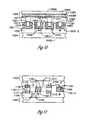
- FIG. 13is a block diagram which illustrates an embodiment of a system 1300 using line signaling according to teachings of the present invention.
- the system 1300includes a low output impedance driver 1310 having a driver impedance, as is well known in the art.
- the low output impedance driver 1310is coupled to a transmission line circuit 1320 .
- Embodiments of the transmission line circuit 1320are described and presented above with reference to FIGS. 6-12 .
- the system 1300includes a termination circuit 1330 having a termination impedance that is matched to the impedance of the transmission line circuit 1320 .
- FIG. 14is a block diagram which illustrates an embodiment of a system 1400 according to teaching of the present invention.
- the system 1400includes an integrated circuit 1410 .
- the integrated circuit 1410includes the transmission line circuit described and presented above with reference to FIGS. 6-12 .
- the system 1400includes a processor 1420 that is operatively coupled to the integrated circuit 1410 .
- the processor 1420is coupled to the integrated circuit 1410 through a system bus 1430 .
- the processor 1420 and the integrated circuit 1410are on the same semiconductor chip.
- test structureswere fabricated having toroidal shapes with widths ranging from 0.5 to 30 ⁇ m.
- Each toroidconsists of two parallel rectangular-shape patterned films connected by “pedestals” at both ends.
- the base designed of the test structure55 ⁇ m long with ten-turn coils.
- the coilsare embedded in alumina and these devices are fully planarized by the chemical-mechanical-polish process to avoid undesirable stress induced by topography.
- the bottom layersare 2.5 ⁇ m thick permalloy and the pedestals are 2.2 ⁇ m tall permalloy.
- One waferhas 2.5 ⁇ m of permalloy and top layers and other Ni 45 Fe 55 .
- the inductance rolloff date of these structuresare measured by using a Hewlett Packard 4291A impedance analyzer.
- the test structuresare excited by applying high frequency current to the pancake coils.
- the permeability frequency rolloff characteristics of the magnetic thin filmswere calculated from the inductance rolloff data by using the segmental transmission line method as described in an article by T. Amoldussen. (See generally, IEEE Trans. Magn ., 24, 2482 (1988)). The simple geometry of these devices minimizes the ambiguity in permeability calculations.
- Permeability of patterned permalloy and Ni 45 Fe 55 films with widths from 30 to 0.5 ⁇ mhas been studied under high field up to 5 Oe and frequency up to 500 MHz. It is observed that the permeability increases as the excitation field increases due to the increasing flux conduction from wall motion. At frequencies where wall motion is damped, there is no discernible difference between high and low field excitation. The data also suggest that the permeability rolloff measured at low excitation current is sufficient to predict high frequency write head performance. As the width of the patterns is reduced, the reduction of effective rotational permeability results from reduction of the active area since the edge closure region does not participate in flux conduction. As the width is reduced to sub-micron range, the rotational permeability is significantly reduced.
- the 0.5 ⁇ m wide devicehas ⁇ rot of 80 for the permalloy case and 50 for the Ni 45 Fe 55 case.
- the magnetic film patternwas designed so as to eliminate demagnetizing field effects, and the permeability was estimated based on analysis of the magnetic circuit. Using this method, NiFe/SiO 2 and (Fe/SiO 2 )/SiO 2 multilayer films were confirmed to show superior frequency characteristics by a factor of 20 over those of NiFe single-layer film. Also, ferromagnetic resonance (FMR) was observed in these multilayer films at 650 and 750 MHz.
- FMRferromagnetic resonance
- a Hewlett Packard HP4191Awas used in impedance measurements. Specialized tubes (16091-60023) were connected to both ends of the sample, and these were mounted inside a cylindrical fixture (16091A) to perform measurements.
- the sample impedanceranged from several Ohms to several ten of Ohms between 10 MHz and 1000 MHz, and above several tens of MHz the instrument measurement error was within several percent.
- CMOS circuitsoffer the following advantages: (1) the signal delay depends only on the velocity of light on the line and is easily predictable and reproducible, eliminating or allowing for compensation for signal and/or clock skew, (2) there are no reflections at the receiving end of the line and this minimizes ringing, and (3) noise signals will be smaller due to weaker coupling between lines resulting in better signal to noise ratios, the noise current will only be a small fraction of the signal current.
Landscapes
- Physics & Mathematics (AREA)
- Condensed Matter Physics & Semiconductors (AREA)
- General Physics & Mathematics (AREA)
- Engineering & Computer Science (AREA)
- Computer Hardware Design (AREA)
- Microelectronics & Electronic Packaging (AREA)
- Power Engineering (AREA)
- Semiconductor Integrated Circuits (AREA)
Abstract
Description
Cint/C=½[ln(4h/a)/ln(2s/a)].
- (i) magnetic shields above and below the lines
- (ii) magnetic shields between lines
- (i) good conductors with a thickness greater than the skin depth, the conventional approach, but one which may not be possible or practical with interconnection lines of sub-micron dimensions
- (ii) shields with high permeability metals to minimize the mutual coupling or inductance between lines
- 1. Through this method, the magnetic circuit composed of an inductance line with a magnetic/conductive/magnetic films structures was analyzed the basis of its impedance characteristics, enabling calculation of the relative permeability of the magnetic material. The inductance line had a stripe shape, and the stray capacitance was reduced to raise the resonance frequency, making possible measurements in the GHz range. By adopting a strip pattern for the magnetic layers, the effect of the demagnetizing field was avoided. In order to perform still more accurate measurements, it will probably be necessary to add improvements to the magnetic circuit analysis and impedance matching.
- 2. It was confirmed that the multilayer structure including none magnetic layers is an effective means of improving the frequency characteristic, reducing losses and expanding the effective magnetic path width. For NiFe/SiO2[50-100 nm] and (Fe/SiO2)SiO2[(7/2.5)/50 nm] multilayer film, an improvement of some twenty times or so over NiFe single-layer film was observed.
- 3. The high-frequency magnetic properties of multilayer film are limited by dielectric breakdown of the insulating layers when the latter are thin, and by eddy current loss due to formation of an electrical capacitance and/or by ferromagnetic resonance when the insulating layer are thick. Ferromagnetic resonance was observed at 650 MHz in the NiFe/SiO2, and at 750 MHz in the (Fe/SiO2)SiO2multilayer films.
Claims (32)
Priority Applications (4)
| Application Number | Priority Date | Filing Date | Title |
|---|---|---|---|
| US10/099,217US7235457B2 (en) | 2002-03-13 | 2002-03-13 | High permeability layered films to reduce noise in high speed interconnects |
| US10/930,657US7375414B2 (en) | 2002-03-13 | 2004-08-31 | High permeability layered films to reduce noise in high speed interconnects |
| US11/492,253US20070029645A1 (en) | 2002-03-13 | 2006-07-25 | High permeability layered films to reduce noise in high speed interconnects |
| US11/492,655US7829979B2 (en) | 2002-03-13 | 2006-07-25 | High permeability layered films to reduce noise in high speed interconnects |
Applications Claiming Priority (1)
| Application Number | Priority Date | Filing Date | Title |
|---|---|---|---|
| US10/099,217US7235457B2 (en) | 2002-03-13 | 2002-03-13 | High permeability layered films to reduce noise in high speed interconnects |
Related Child Applications (1)
| Application Number | Title | Priority Date | Filing Date |
|---|---|---|---|
| US10/930,657DivisionUS7375414B2 (en) | 2002-03-13 | 2004-08-31 | High permeability layered films to reduce noise in high speed interconnects |
Publications (2)
| Publication Number | Publication Date |
|---|---|
| US20030174529A1 US20030174529A1 (en) | 2003-09-18 |
| US7235457B2true US7235457B2 (en) | 2007-06-26 |
Family
ID=28039535
Family Applications (4)
| Application Number | Title | Priority Date | Filing Date |
|---|---|---|---|
| US10/099,217Expired - LifetimeUS7235457B2 (en) | 2002-03-13 | 2002-03-13 | High permeability layered films to reduce noise in high speed interconnects |
| US10/930,657Expired - LifetimeUS7375414B2 (en) | 2002-03-13 | 2004-08-31 | High permeability layered films to reduce noise in high speed interconnects |
| US11/492,655Expired - LifetimeUS7829979B2 (en) | 2002-03-13 | 2006-07-25 | High permeability layered films to reduce noise in high speed interconnects |
| US11/492,253AbandonedUS20070029645A1 (en) | 2002-03-13 | 2006-07-25 | High permeability layered films to reduce noise in high speed interconnects |
Family Applications After (3)
| Application Number | Title | Priority Date | Filing Date |
|---|---|---|---|
| US10/930,657Expired - LifetimeUS7375414B2 (en) | 2002-03-13 | 2004-08-31 | High permeability layered films to reduce noise in high speed interconnects |
| US11/492,655Expired - LifetimeUS7829979B2 (en) | 2002-03-13 | 2006-07-25 | High permeability layered films to reduce noise in high speed interconnects |
| US11/492,253AbandonedUS20070029645A1 (en) | 2002-03-13 | 2006-07-25 | High permeability layered films to reduce noise in high speed interconnects |
Country Status (1)
| Country | Link |
|---|---|
| US (4) | US7235457B2 (en) |
Cited By (11)
| Publication number | Priority date | Publication date | Assignee | Title |
|---|---|---|---|---|
| US20050007817A1 (en)* | 2002-03-13 | 2005-01-13 | Micron Technology, Inc. | High permeability composite films to reduce noise in high speed interconnects |
| US20050030803A1 (en)* | 2002-03-13 | 2005-02-10 | Micron Technology, Inc. | High permeability layered films to reduce noise in high speed interconnects |
| US20050030780A1 (en)* | 2002-02-06 | 2005-02-10 | Infineon Technologies Ag | Memory cell |
| US20060244108A1 (en)* | 2002-01-30 | 2006-11-02 | Micron Technology, Inc. | Capacitive techniques to reduce noise in high speed interconnections |
| US20070111576A1 (en)* | 2005-11-17 | 2007-05-17 | International Business Machines Corporation | Circuit on a printed circuit board |
| US20090107710A1 (en)* | 2007-10-26 | 2009-04-30 | Force10 Networks, Inc. | Differential trace profile for printed circult boards |
| US7554829B2 (en) | 1999-07-30 | 2009-06-30 | Micron Technology, Inc. | Transmission lines for CMOS integrated circuits |
| US20100258338A1 (en)* | 2009-04-13 | 2010-10-14 | Hon Hai Precision Industry Co., Ltd. | Flexible printed circuit board |
| US8168891B1 (en)* | 2007-10-26 | 2012-05-01 | Force10 Networks, Inc. | Differential trace profile for printed circuit boards |
| US20160029477A1 (en)* | 2013-02-27 | 2016-01-28 | Nec Corporation | Wiring substrate, semiconductor device, printed board, and method for producing wiring substrate |
| US20180048094A1 (en)* | 2014-05-08 | 2018-02-15 | Apple Inc. | Connector system impedance matching |
Families Citing this family (18)
| Publication number | Priority date | Publication date | Assignee | Title |
|---|---|---|---|---|
| US6373740B1 (en)* | 1999-07-30 | 2002-04-16 | Micron Technology, Inc. | Transmission lines for CMOS integrated circuits |
| US7160577B2 (en) | 2002-05-02 | 2007-01-09 | Micron Technology, Inc. | Methods for atomic-layer deposition of aluminum oxides in integrated circuits |
| US7589029B2 (en) | 2002-05-02 | 2009-09-15 | Micron Technology, Inc. | Atomic layer deposition and conversion |
| US7135421B2 (en) | 2002-06-05 | 2006-11-14 | Micron Technology, Inc. | Atomic layer-deposited hafnium aluminum oxide |
| US7192892B2 (en) | 2003-03-04 | 2007-03-20 | Micron Technology, Inc. | Atomic layer deposited dielectric layers |
| US6970053B2 (en)* | 2003-05-22 | 2005-11-29 | Micron Technology, Inc. | Atomic layer deposition (ALD) high permeability layered magnetic films to reduce noise in high speed interconnection |
| US20060072257A1 (en)* | 2004-09-30 | 2006-04-06 | International Business Machines Corporation | Device and method for reducing dishing of critical on-chip interconnect lines |
| US8943456B2 (en) | 2004-09-30 | 2015-01-27 | International Business Machines Corporation | Layout determining for wide wire on-chip interconnect lines |
| US7560395B2 (en) | 2005-01-05 | 2009-07-14 | Micron Technology, Inc. | Atomic layer deposited hafnium tantalum oxide dielectrics |
| US7927948B2 (en) | 2005-07-20 | 2011-04-19 | Micron Technology, Inc. | Devices with nanocrystals and methods of formation |
| JP4618599B2 (en)* | 2005-08-29 | 2011-01-26 | エルピーダメモリ株式会社 | Semiconductor module |
| JP5082329B2 (en)* | 2006-08-10 | 2012-11-28 | 富士電機株式会社 | DC-DC converter |
| US7605030B2 (en) | 2006-08-31 | 2009-10-20 | Micron Technology, Inc. | Hafnium tantalum oxynitride high-k dielectric and metal gates |
| EP2040427A1 (en)* | 2007-09-22 | 2009-03-25 | New Day Investment Limited | High speed electrical data transmission system |
| US8198895B2 (en)* | 2009-09-23 | 2012-06-12 | General Electric Company | System and method for magnetic resonance coil actuation |
| US8664743B1 (en)* | 2012-10-31 | 2014-03-04 | Taiwan Semiconductor Manufacturing Company, Ltd. | Air-gap formation in interconnect structures |
| KR101416159B1 (en)* | 2013-09-06 | 2014-07-14 | 주식회사 기가레인 | Printed curcuit board comprising contact pad |
| WO2019074470A1 (en)* | 2017-10-09 | 2019-04-18 | Keysight Technologies, Inc. | Hybrid coaxial cable fabrication |
Citations (63)
| Publication number | Priority date | Publication date | Assignee | Title |
|---|---|---|---|---|
| US3816673A (en) | 1971-01-25 | 1974-06-11 | Kokusai Denshin Denwa Co Ltd | Coaxial cable including at least one repeater |
| US3923567A (en) | 1974-08-09 | 1975-12-02 | Silicon Materials Inc | Method of reclaiming a semiconductor wafer |
| US4308421A (en) | 1978-01-18 | 1981-12-29 | Virginia Plastics Company | EMF Controlled multi-conductor cable |
| US4372032A (en)* | 1979-09-04 | 1983-02-08 | The United States Of America As Represented By The Secretary Of The Navy | Normally off InP field effect transistor making process |
| US4601021A (en) | 1982-04-12 | 1986-07-15 | Tektronix, Inc. | Highlighting and classifying segments on a CRT display |
| US4640871A (en) | 1984-09-12 | 1987-02-03 | Sony Corporation | Magnetic material having high permeability in the high frequency range |
| US4710798A (en) | 1985-09-10 | 1987-12-01 | Northern Telecom Limited | Integrated circuit chip package |
| US4749888A (en) | 1984-01-25 | 1988-06-07 | Agency Of Industrial Science & Technology | Josephson transmission line device |
| US4933743A (en) | 1989-03-11 | 1990-06-12 | Fairchild Semiconductor Corporation | High performance interconnect system for an integrated circuit |
| US4962476A (en)* | 1988-07-26 | 1990-10-09 | Nec Corporation | Semiconductor memory device having bit lines less liable to have influences of the adjacent bit lines |
| US5019728A (en) | 1990-09-10 | 1991-05-28 | Ncr Corporation | High speed CMOS backpanel transceiver |
| US5073771A (en) | 1988-03-02 | 1991-12-17 | Hitachi, Ltd. | Control method of zooming screen |
| US5128962A (en) | 1989-06-16 | 1992-07-07 | Texas Instruments Incorporated | Line interface circuit and a method of testing such a circuit |
| US5135889A (en) | 1991-12-09 | 1992-08-04 | Micron Technology, Inc. | Method for forming a shielding structure for decoupling signal traces in a semiconductor |
| US5157361A (en) | 1991-05-10 | 1992-10-20 | Gruchalla Michael E | Nonlinear transmission line |
| US5165046A (en) | 1989-11-06 | 1992-11-17 | Micron Technology, Inc. | High speed CMOS driver circuit |
| US5168334A (en) | 1987-07-31 | 1992-12-01 | Texas Instruments, Incorporated | Non-volatile semiconductor memory |
| US5223808A (en) | 1992-02-25 | 1993-06-29 | Hughes Aircraft Company | Planar ferrite phase shifter |
| US5258648A (en) | 1991-06-27 | 1993-11-02 | Motorola, Inc. | Composite flip chip semiconductor device with an interposer having test contacts formed along its periphery |
| US5343366A (en) | 1992-06-24 | 1994-08-30 | International Business Machines Corporation | Packages for stacked integrated circuit chip cubes |
| US5357138A (en) | 1991-02-22 | 1994-10-18 | Nec Corporation | Coaxial wiring pattern structure in a multilayered wiring board |
| US5363550A (en) | 1992-12-23 | 1994-11-15 | International Business Machines Corporation | Method of Fabricating a micro-coaxial wiring structure |
| US5391917A (en) | 1993-05-10 | 1995-02-21 | International Business Machines Corporation | Multiprocessor module packaging |
| US5450026A (en) | 1994-07-27 | 1995-09-12 | At&T Corp. | Current mode driver for differential bus |
| US5468681A (en) | 1989-08-28 | 1995-11-21 | Lsi Logic Corporation | Process for interconnecting conductive substrates using an interposer having conductive plastic filled vias |
| US5510758A (en) | 1993-04-07 | 1996-04-23 | Matsushita Electric Industrial Co., Ltd. | Multilayer microstrip wiring board with a semiconductor device mounted thereon via bumps |
| US5521536A (en) | 1993-08-06 | 1996-05-28 | Hitachi, Ltd. | Integrated circuit device having different signal transfer circuits for wirings with different lengths |
| US5567654A (en) | 1994-09-28 | 1996-10-22 | International Business Machines Corporation | Method and workpiece for connecting a thin layer to a monolithic electronic module's surface and associated module packaging |
| US5574923A (en) | 1993-05-10 | 1996-11-12 | Intel Corporation | Method and apparatus for performing bi-endian byte and short accesses in a single-endian microprocessor |
| US5619159A (en) | 1991-01-10 | 1997-04-08 | Fujitsu Limited | Signal processing device and a method for transmitting signal |
| US5622875A (en) | 1994-05-06 | 1997-04-22 | Kobe Precision, Inc. | Method for reclaiming substrate from semiconductor wafers |
| US5637828A (en) | 1993-10-08 | 1997-06-10 | Texas Instruments Inc. | High density semiconductor package |
| US5663596A (en) | 1995-12-21 | 1997-09-02 | Hughes Electronics | Integrated circuit spring contacts |
| US5772153A (en) | 1995-10-17 | 1998-06-30 | Abaunza; John T. | Aircraft icing sensors |
| US5811984A (en) | 1995-10-05 | 1998-09-22 | The Regents Of The University Of California | Current mode I/O for digital circuits |
| US5834799A (en) | 1989-08-28 | 1998-11-10 | Lsi Logic | Optically transmissive preformed planar structures |
| US5855735A (en) | 1995-10-03 | 1999-01-05 | Kobe Precision, Inc. | Process for recovering substrates |
| US5861666A (en) | 1995-08-30 | 1999-01-19 | Tessera, Inc. | Stacked chip assembly |
| US5880601A (en) | 1994-06-13 | 1999-03-09 | Hitachi, Ltd. | Signal receiving circuit and digital signal processing system |
| US5910684A (en) | 1995-11-03 | 1999-06-08 | Micron Technology, Inc. | Integrated circuitry |
| US5991161A (en) | 1997-12-19 | 1999-11-23 | Intel Corporation | Multi-chip land grid array carrier |
| US5990564A (en) | 1997-05-30 | 1999-11-23 | Lucent Technologies Inc. | Flip chip packaging of memory chips |
| US6016256A (en) | 1997-11-14 | 2000-01-18 | The Panda Project | Multi-chip module having interconnect dies |
| US6022787A (en)* | 1996-03-25 | 2000-02-08 | Micron Technology, Inc. | Method of making a structure for providing signal isolation and decoupling in an integrated circuit device |
| US6075383A (en) | 1995-04-28 | 2000-06-13 | Siemens Aktiengesellschaft | GTL output amplifier for coupling an input signal present at the input into a transmission line present at the output |
| US6133621A (en)* | 1998-10-15 | 2000-10-17 | Stmicroelectronics S.R.L. | Integrated shielded electric connection |
| US6143616A (en) | 1997-08-22 | 2000-11-07 | Micron Technology, Inc. | Methods of forming coaxial integrated circuitry interconnect lines |
| US6181004B1 (en) | 1999-01-22 | 2001-01-30 | Jerry D. Koontz | Digital signal processing assembly and test method |
| US20010000428A1 (en) | 1999-02-23 | 2001-04-26 | Abadeer Wagdi W. | Termination resistance independent system for impedance matching in high speed input-output chip interfacing |
| US6226599B1 (en) | 1997-03-05 | 2001-05-01 | Fujitsu Limted | Electromagnetic wave analyzer apparatus |
| US6242796B1 (en) | 1996-12-06 | 2001-06-05 | Hyundai Electronics Industries Co., Ltd. | Wiring structure of semiconductor memory device and formation method thereof |
| US6255852B1 (en) | 1999-02-09 | 2001-07-03 | Micron Technology, Inc. | Current mode signal interconnects and CMOS amplifier |
| US6281042B1 (en) | 1998-08-31 | 2001-08-28 | Micron Technology, Inc. | Structure and method for a high performance electronic packaging assembly |
| US6373740B1 (en) | 1999-07-30 | 2002-04-16 | Micron Technology, Inc. | Transmission lines for CMOS integrated circuits |
| US6388198B1 (en) | 1999-03-09 | 2002-05-14 | International Business Machines Corporation | Coaxial wiring within SOI semiconductor, PCB to system for high speed operation and signal quality |
| US6420778B1 (en) | 2001-06-01 | 2002-07-16 | Aralight, Inc. | Differential electrical transmission line structures employing crosstalk compensation and related methods |
| US6433408B1 (en) | 1999-01-08 | 2002-08-13 | Nec Corporation | Highly integrated circuit including transmission lines which have excellent characteristics |
| US6545338B1 (en)* | 1999-10-28 | 2003-04-08 | Koninklijke Philips Electronics N.V. | Methods for implementing co-axial interconnect lines in a CMOS process for high speed RF and microwave applications |
| US6555858B1 (en) | 2000-11-15 | 2003-04-29 | Motorola, Inc. | Self-aligned magnetic clad write line and its method of formation |
| US6569757B1 (en)* | 1999-10-28 | 2003-05-27 | Philips Electronics North America Corporation | Methods for forming co-axial interconnect lines in a CMOS process for high speed applications |
| US20030176023A1 (en) | 2002-03-13 | 2003-09-18 | Micron Technology, Inc. | High permeability composite films to reduce noise in high speed interconnects |
| US20030176050A1 (en) | 2002-03-13 | 2003-09-18 | Micron Technology Inc. | High permeability thin films and patterned thin films to reduce noise in high speed interconnections |
| US6692898B2 (en) | 2001-01-24 | 2004-02-17 | Infineon Technologies Ag | Self-aligned conductive line for cross-point magnetic memory integrated circuits |
Family Cites Families (94)
| Publication number | Priority date | Publication date | Assignee | Title |
|---|---|---|---|---|
| US673788A (en)* | 1899-03-23 | 1901-05-07 | D M Osborne & Co | Spring-tooth harrow. |
| US3383526A (en) | 1964-12-17 | 1968-05-14 | Ibm | Current driver circuit utilizing transistors |
| US3478230A (en)* | 1967-04-17 | 1969-11-11 | United Aircraft Corp | Thermomagnetic generation of power in a superconductor |
| US3743550A (en)* | 1970-06-25 | 1973-07-03 | Elect & Magn Alloys Res Inst | Alloys for magnetic recording-reproducing heads |
| US3676718A (en)* | 1971-03-26 | 1972-07-11 | Bell Telephone Labor Inc | Supercurrent structures utilizing mobil flux vortices |
| US3716673A (en)* | 1971-11-29 | 1973-02-13 | Electrospace Corp | Answering machine telephone line coupling device |
| US3982268A (en) | 1973-10-30 | 1976-09-21 | General Electric Company | Deep diode lead throughs |
| US3959047A (en) | 1974-09-30 | 1976-05-25 | International Business Machines Corporation | Method for constructing a rom for redundancy and other applications |
| US3925593A (en)* | 1974-11-11 | 1975-12-09 | Honeywell Inc | Monotonically changing skew in a magnetostrictive anisotropic thin film plated wire line sensor |
| US4081701A (en) | 1976-06-01 | 1978-03-28 | Texas Instruments Incorporated | High speed sense amplifier for MOS random access memory |
| US4339305A (en)* | 1981-02-05 | 1982-07-13 | Rockwell International Corporation | Planar circuit fabrication by plating and liftoff |
| US4394712A (en) | 1981-03-18 | 1983-07-19 | General Electric Company | Alignment-enhancing feed-through conductors for stackable silicon-on-sapphire wafers |
| JPS60134461A (en) | 1983-12-23 | 1985-07-17 | Hitachi Ltd | semiconductor storage device |
| US4595428A (en) | 1984-01-03 | 1986-06-17 | General Electric Company | Method for producing high-aspect ratio hollow diffused regions in a semiconductor body |
| US4631636A (en) | 1984-03-26 | 1986-12-23 | Harris Corporation | High density packaging technique for electronic systems |
| US4713841A (en) | 1985-06-03 | 1987-12-15 | Itt Electro Optical Products, A Division Of Itt Corporation | Synchronous, asynchronous, data rate transparent fiber optic communications link |
| US4739446A (en) | 1986-05-05 | 1988-04-19 | Itt Defense Communications, A Division Of Itt Corporation | Header for a wafer scale assembly |
| US4977439A (en) | 1987-04-03 | 1990-12-11 | Esquivel Agerico L | Buried multilevel interconnect system |
| US4870470A (en) | 1987-10-16 | 1989-09-26 | International Business Machines Corporation | Non-volatile memory cell having Si rich silicon nitride charge trapping layer |
| US4994688A (en) | 1988-05-25 | 1991-02-19 | Hitachi Ltd. | Semiconductor device having a reference voltage generating circuit |
| US5061987A (en) | 1990-01-09 | 1991-10-29 | Northrop Corporation | Silicon substrate multichip assembly |
| IL96808A (en) | 1990-04-18 | 1996-03-31 | Rambus Inc | Integrated circuit i/o using a high performance bus interface |
| US5079618A (en) | 1990-06-12 | 1992-01-07 | Micron Technology, Inc. | Semiconductor device structures cooled by Peltier junctions and electrical interconnect assemblies |
| US5229327A (en) | 1990-06-12 | 1993-07-20 | Micron Technology, Inc. | Process for manufacturing semiconductor device structures cooled by Peltier junctions and electrical interconnect assemblies therefor |
| US5781746A (en) | 1990-07-20 | 1998-07-14 | Siemens Aktiengesellschaft | Microprocessor with multiple bus configurations |
| ATE105458T1 (en) | 1990-08-03 | 1994-05-15 | Siemens Nixdorf Inf Syst | INSTALLATION SYSTEM FOR ELECTRICAL FUNCTIONAL UNITS, ESPECIALLY FOR DATA TECHNOLOGY. |
| JP2960560B2 (en) | 1991-02-28 | 1999-10-06 | 株式会社日立製作所 | Microelectronic equipment |
| JP3133490B2 (en) | 1991-08-27 | 2001-02-05 | 古河電気工業株式会社 | Multiplex transmission equipment |
| US5275001A (en) | 1991-10-07 | 1994-01-04 | Matsushita Electric Industrial Co., Ltd. | Thermoelectric cooling device |
| JP2692461B2 (en) | 1991-10-26 | 1997-12-17 | 日本電気株式会社 | Semiconductor device |
| JPH05129666A (en) | 1991-11-02 | 1993-05-25 | Shinko Electric Ind Co Ltd | Semiconductor device |
| DE4345604B3 (en) | 1992-03-06 | 2012-07-12 | Rambus Inc. | Device for communication with a DRAM |
| US5438224A (en) | 1992-04-23 | 1995-08-01 | Motorola, Inc. | Integrated circuit package having a face-to-face IC chip arrangement |
| WO1994005039A1 (en) | 1992-08-20 | 1994-03-03 | Capps David A | Semiconductor wafer for lamination applications |
| JP3451107B2 (en) | 1992-10-05 | 2003-09-29 | 株式会社エコ・トゥエンティーワン | Electronic cooling device |
| JPH06125208A (en) | 1992-10-09 | 1994-05-06 | Mitsubishi Electric Corp | Microwave integrated circuit and its production |
| US5232863A (en) | 1992-10-20 | 1993-08-03 | Micron Semiconductor, Inc. | Method of forming electrical contact between a field effect transistor gate and a remote active area |
| US5392407A (en) | 1992-12-24 | 1995-02-21 | Ncr Corporation | Multi-port processor with peripheral component interconnect port and rambus port |
| US5415699A (en) | 1993-01-12 | 1995-05-16 | Massachusetts Institute Of Technology | Superlattice structures particularly suitable for use as thermoelectric cooling materials |
| US5598039A (en) | 1993-03-15 | 1997-01-28 | Touchstone Patent Trust | Method and apparatus for sensing state of electric power flow through a master circuit and producing remote control of a slave circuit |
| US5313361A (en) | 1993-03-29 | 1994-05-17 | The Charles Stark Draper Laboratory, Inc. | Ceramic substrate |
| DE4314907C1 (en) | 1993-05-05 | 1994-08-25 | Siemens Ag | Method for producing semiconductor components making electrically conducting contact with one another vertically |
| JP2771423B2 (en) | 1993-05-20 | 1998-07-02 | 日本電気株式会社 | Bipolar transistor |
| US5598031A (en) | 1993-06-23 | 1997-01-28 | Vlsi Technology, Inc. | Electrically and thermally enhanced package using a separate silicon substrate |
| US5610366A (en) | 1993-08-03 | 1997-03-11 | California Institute Of Technology | High performance thermoelectric materials and methods of preparation |
| EP0721662A1 (en) | 1993-09-30 | 1996-07-17 | Kopin Corporation | Three-dimensional processor using transferred thin film circuits |
| JP2867859B2 (en) | 1993-12-13 | 1999-03-10 | 日本電気株式会社 | Optical transceiver module for bidirectional transmission |
| US5753529A (en) | 1994-05-05 | 1998-05-19 | Siliconix Incorporated | Surface mount and flip chip technology for total integrated circuit isolation |
| US5902118A (en) | 1994-07-05 | 1999-05-11 | Siemens Aktiengesellschaft | Method for production of a three-dimensional circuit arrangement |
| US5521406A (en) | 1994-08-31 | 1996-05-28 | Texas Instruments Incorporated | Integrated circuit with improved thermal impedance |
| US5587119A (en) | 1994-09-14 | 1996-12-24 | E-Systems, Inc. | Method for manufacturing a coaxial interconnect |
| US5661427A (en) | 1994-10-05 | 1997-08-26 | Micro Linear Corporation | Series terminated clock deskewing apparatus |
| US5646067A (en) | 1995-06-05 | 1997-07-08 | Harris Corporation | Method of bonding wafers having vias including conductive material |
| US5618752A (en) | 1995-06-05 | 1997-04-08 | Harris Corporation | Method of fabrication of surface mountable integrated circuits |
| US5682062A (en) | 1995-06-05 | 1997-10-28 | Harris Corporation | System for interconnecting stacked integrated circuits |
| US5955786A (en) | 1995-06-07 | 1999-09-21 | Advanced Micro Devices, Inc. | Semiconductor device using uniform nonconformal deposition for forming low dielectric constant insulation between certain conductive lines |
| US5872393A (en) | 1995-10-30 | 1999-02-16 | Matsushita Electric Industrial Co., Ltd. | RF semiconductor device and a method for manufacturing the same |
| US5714791A (en) | 1995-12-22 | 1998-02-03 | International Business Machines Corporation | On-chip Peltier cooling devices on a micromachined membrane structure |
| US6224690B1 (en)* | 1995-12-22 | 2001-05-01 | International Business Machines Corporation | Flip-Chip interconnections using lead-free solders |
| JPH09266289A (en) | 1996-03-29 | 1997-10-07 | Mitsubishi Electric Corp | Semiconductor memory device and method of manufacturing the same |
| US5903045A (en) | 1996-04-30 | 1999-05-11 | International Business Machines Corporation | Self-aligned connector for stacked chip module |
| US5692558A (en) | 1996-07-22 | 1997-12-02 | Northrop Grumman Corporation | Microchannel cooling using aviation fuels for airborne electronics |
| JPH1065034A (en) | 1996-08-21 | 1998-03-06 | Ngk Spark Plug Co Ltd | Wiring substrate for electronic parts and package of electronic parts |
| JP2933129B2 (en) | 1996-09-06 | 1999-08-09 | ファナック株式会社 | Robot controller |
| US5807783A (en) | 1996-10-07 | 1998-09-15 | Harris Corporation | Surface mount die by handle replacement |
| JP2914342B2 (en) | 1997-03-28 | 1999-06-28 | 日本電気株式会社 | Cooling structure of integrated circuit device |
| US5915167A (en) | 1997-04-04 | 1999-06-22 | Elm Technology Corporation | Three dimensional structure memory |
| US6221913B1 (en)* | 1998-01-21 | 2001-04-24 | Zymogenetics, Inc. | Dialkyl ureas as calcitonin mimetics |
| US6137164A (en) | 1998-03-16 | 2000-10-24 | Texas Instruments Incorporated | Thin stacked integrated circuit device |
| US6161215A (en) | 1998-08-31 | 2000-12-12 | Hewlett-Packard Company | Package routing of integrated circuit signals |
| US6219237B1 (en) | 1998-08-31 | 2001-04-17 | Micron Technology, Inc. | Structure and method for an electronic assembly |
| JP3180785B2 (en)* | 1998-11-27 | 2001-06-25 | 日本電気株式会社 | Yoke type magnetoresistive head, yoke type magnetoresistive composite thin film head, and magnetic storage device |
| US6373674B1 (en) | 1999-03-24 | 2002-04-16 | Masprodenkoh Kabushikikaisha | Noise eliminating apparatus of high-frequency transmission system |
| US7554829B2 (en) | 1999-07-30 | 2009-06-30 | Micron Technology, Inc. | Transmission lines for CMOS integrated circuits |
| JP2001201521A (en)* | 2000-01-18 | 2001-07-27 | Agilent Technologies Japan Ltd | Current detecting device and impedance measuring apparatus and power measuring device |
| JP3322861B2 (en)* | 2000-02-21 | 2002-09-09 | スタンレー電気株式会社 | Variable phase device |
| US6727105B1 (en)* | 2000-02-28 | 2004-04-27 | Hewlett-Packard Development Company, L.P. | Method of fabricating an MRAM device including spin dependent tunneling junction memory cells |
| US6225935B1 (en) | 2000-03-16 | 2001-05-01 | Mmtc, Inc. | Biphase-encoded signal processing employing passive and/or semi-passive transistor circuits |
| US6674167B1 (en) | 2000-05-31 | 2004-01-06 | Micron Technology, Inc. | Multilevel copper interconnect with double passivation |
| US6515352B1 (en)* | 2000-09-25 | 2003-02-04 | Micron Technology, Inc. | Shielding arrangement to protect a circuit from stray magnetic fields |
| US6350649B1 (en)* | 2000-10-30 | 2002-02-26 | Samsung Electronics Co., Ltd. | Bit line landing pad and borderless contact on bit line stud with etch stop layer and manufacturing method thereof |
| US6787906B1 (en)* | 2000-10-30 | 2004-09-07 | Samsung Electronics Co., Ltd. | Bit line pad and borderless contact on bit line stud with localized etch stop layer formed in an undermined region |
| US6518671B1 (en)* | 2000-10-30 | 2003-02-11 | Samsung Electronics Co. Ltd. | Bit line landing pad and borderless contact on bit line stud with localized etch stop layer and manufacturing method thereof |
| JP4462758B2 (en) | 2000-12-27 | 2010-05-12 | 京セラ株式会社 | High frequency wiring board |
| EP1397588B1 (en)* | 2001-06-21 | 2006-01-04 | ALSTOM Technology Ltd | Method for operating an internal combustion engine |
| CN1174443C (en) | 2001-07-19 | 2004-11-03 | 清华同方股份有限公司 | Method for preparing VHF chip sensor material |
| US6603080B2 (en)* | 2001-09-27 | 2003-08-05 | Andrew Corporation | Circuit board having ferrite powder containing layer |
| US6806630B2 (en) | 2002-01-09 | 2004-10-19 | Hewlett-Packard Development Company, L.P. | Electron emitter device for data storage applications and method of manufacture |
| US7101770B2 (en)* | 2002-01-30 | 2006-09-05 | Micron Technology, Inc. | Capacitive techniques to reduce noise in high speed interconnections |
| US7235457B2 (en)* | 2002-03-13 | 2007-06-26 | Micron Technology, Inc. | High permeability layered films to reduce noise in high speed interconnects |
| US6756237B2 (en)* | 2002-03-25 | 2004-06-29 | Brown University Research Foundation | Reduction of noise, and optimization of magnetic field sensitivity and electrical properties in magnetic tunnel junction devices |
| JP4133472B2 (en) | 2003-03-11 | 2008-08-13 | 三菱農機株式会社 | Paddy field work vehicle |
| US6970053B2 (en)* | 2003-05-22 | 2005-11-29 | Micron Technology, Inc. | Atomic layer deposition (ALD) high permeability layered magnetic films to reduce noise in high speed interconnection |
| US6940462B2 (en)* | 2003-09-19 | 2005-09-06 | Harris Corporation | Broadband dipole antenna to be worn by a user and associated methods |
- 2002
- 2002-03-13USUS10/099,217patent/US7235457B2/ennot_activeExpired - Lifetime
- 2004
- 2004-08-31USUS10/930,657patent/US7375414B2/ennot_activeExpired - Lifetime
- 2006
- 2006-07-25USUS11/492,655patent/US7829979B2/ennot_activeExpired - Lifetime
- 2006-07-25USUS11/492,253patent/US20070029645A1/ennot_activeAbandoned
Patent Citations (67)
| Publication number | Priority date | Publication date | Assignee | Title |
|---|---|---|---|---|
| US3816673A (en) | 1971-01-25 | 1974-06-11 | Kokusai Denshin Denwa Co Ltd | Coaxial cable including at least one repeater |
| US3923567A (en) | 1974-08-09 | 1975-12-02 | Silicon Materials Inc | Method of reclaiming a semiconductor wafer |
| US4308421A (en) | 1978-01-18 | 1981-12-29 | Virginia Plastics Company | EMF Controlled multi-conductor cable |
| US4372032A (en)* | 1979-09-04 | 1983-02-08 | The United States Of America As Represented By The Secretary Of The Navy | Normally off InP field effect transistor making process |
| US4601021A (en) | 1982-04-12 | 1986-07-15 | Tektronix, Inc. | Highlighting and classifying segments on a CRT display |
| US4749888A (en) | 1984-01-25 | 1988-06-07 | Agency Of Industrial Science & Technology | Josephson transmission line device |
| US4640871A (en) | 1984-09-12 | 1987-02-03 | Sony Corporation | Magnetic material having high permeability in the high frequency range |
| US4710798A (en) | 1985-09-10 | 1987-12-01 | Northern Telecom Limited | Integrated circuit chip package |
| US5168334A (en) | 1987-07-31 | 1992-12-01 | Texas Instruments, Incorporated | Non-volatile semiconductor memory |
| US5073771A (en) | 1988-03-02 | 1991-12-17 | Hitachi, Ltd. | Control method of zooming screen |
| US4962476A (en)* | 1988-07-26 | 1990-10-09 | Nec Corporation | Semiconductor memory device having bit lines less liable to have influences of the adjacent bit lines |
| US4933743A (en) | 1989-03-11 | 1990-06-12 | Fairchild Semiconductor Corporation | High performance interconnect system for an integrated circuit |
| US5128962A (en) | 1989-06-16 | 1992-07-07 | Texas Instruments Incorporated | Line interface circuit and a method of testing such a circuit |
| US5834799A (en) | 1989-08-28 | 1998-11-10 | Lsi Logic | Optically transmissive preformed planar structures |
| US5821624A (en) | 1989-08-28 | 1998-10-13 | Lsi Logic Corporation | Semiconductor device assembly techniques using preformed planar structures |
| US5468681A (en) | 1989-08-28 | 1995-11-21 | Lsi Logic Corporation | Process for interconnecting conductive substrates using an interposer having conductive plastic filled vias |
| US5165046A (en) | 1989-11-06 | 1992-11-17 | Micron Technology, Inc. | High speed CMOS driver circuit |
| US5019728A (en) | 1990-09-10 | 1991-05-28 | Ncr Corporation | High speed CMOS backpanel transceiver |
| US5619159A (en) | 1991-01-10 | 1997-04-08 | Fujitsu Limited | Signal processing device and a method for transmitting signal |
| US5357138A (en) | 1991-02-22 | 1994-10-18 | Nec Corporation | Coaxial wiring pattern structure in a multilayered wiring board |
| US5157361A (en) | 1991-05-10 | 1992-10-20 | Gruchalla Michael E | Nonlinear transmission line |
| US5258648A (en) | 1991-06-27 | 1993-11-02 | Motorola, Inc. | Composite flip chip semiconductor device with an interposer having test contacts formed along its periphery |
| US5135889A (en) | 1991-12-09 | 1992-08-04 | Micron Technology, Inc. | Method for forming a shielding structure for decoupling signal traces in a semiconductor |
| US5223808A (en) | 1992-02-25 | 1993-06-29 | Hughes Aircraft Company | Planar ferrite phase shifter |
| US5343366A (en) | 1992-06-24 | 1994-08-30 | International Business Machines Corporation | Packages for stacked integrated circuit chip cubes |
| US5363550A (en) | 1992-12-23 | 1994-11-15 | International Business Machines Corporation | Method of Fabricating a micro-coaxial wiring structure |
| US5510758A (en) | 1993-04-07 | 1996-04-23 | Matsushita Electric Industrial Co., Ltd. | Multilayer microstrip wiring board with a semiconductor device mounted thereon via bumps |
| US5391917A (en) | 1993-05-10 | 1995-02-21 | International Business Machines Corporation | Multiprocessor module packaging |
| US5574923A (en) | 1993-05-10 | 1996-11-12 | Intel Corporation | Method and apparatus for performing bi-endian byte and short accesses in a single-endian microprocessor |
| US5521536A (en) | 1993-08-06 | 1996-05-28 | Hitachi, Ltd. | Integrated circuit device having different signal transfer circuits for wirings with different lengths |
| US5637828A (en) | 1993-10-08 | 1997-06-10 | Texas Instruments Inc. | High density semiconductor package |
| US5622875A (en) | 1994-05-06 | 1997-04-22 | Kobe Precision, Inc. | Method for reclaiming substrate from semiconductor wafers |
| US5880601A (en) | 1994-06-13 | 1999-03-09 | Hitachi, Ltd. | Signal receiving circuit and digital signal processing system |
| US5450026A (en) | 1994-07-27 | 1995-09-12 | At&T Corp. | Current mode driver for differential bus |
| US5786628A (en) | 1994-09-28 | 1998-07-28 | International Business Machines Corporation | Method and workpiece for connecting a thin layer to a monolithic electronic modules surface and associated module packaging |
| US5567654A (en) | 1994-09-28 | 1996-10-22 | International Business Machines Corporation | Method and workpiece for connecting a thin layer to a monolithic electronic module's surface and associated module packaging |
| US6075383A (en) | 1995-04-28 | 2000-06-13 | Siemens Aktiengesellschaft | GTL output amplifier for coupling an input signal present at the input into a transmission line present at the output |
| US5861666A (en) | 1995-08-30 | 1999-01-19 | Tessera, Inc. | Stacked chip assembly |
| US5855735A (en) | 1995-10-03 | 1999-01-05 | Kobe Precision, Inc. | Process for recovering substrates |
| US5811984A (en) | 1995-10-05 | 1998-09-22 | The Regents Of The University Of California | Current mode I/O for digital circuits |
| US5772153A (en) | 1995-10-17 | 1998-06-30 | Abaunza; John T. | Aircraft icing sensors |
| US5910684A (en) | 1995-11-03 | 1999-06-08 | Micron Technology, Inc. | Integrated circuitry |
| US5663596A (en) | 1995-12-21 | 1997-09-02 | Hughes Electronics | Integrated circuit spring contacts |
| US6022787A (en)* | 1996-03-25 | 2000-02-08 | Micron Technology, Inc. | Method of making a structure for providing signal isolation and decoupling in an integrated circuit device |
| US6242796B1 (en) | 1996-12-06 | 2001-06-05 | Hyundai Electronics Industries Co., Ltd. | Wiring structure of semiconductor memory device and formation method thereof |
| US6226599B1 (en) | 1997-03-05 | 2001-05-01 | Fujitsu Limted | Electromagnetic wave analyzer apparatus |
| US5990564A (en) | 1997-05-30 | 1999-11-23 | Lucent Technologies Inc. | Flip chip packaging of memory chips |
| US6143616A (en) | 1997-08-22 | 2000-11-07 | Micron Technology, Inc. | Methods of forming coaxial integrated circuitry interconnect lines |
| US6016256A (en) | 1997-11-14 | 2000-01-18 | The Panda Project | Multi-chip module having interconnect dies |
| US5991161A (en) | 1997-12-19 | 1999-11-23 | Intel Corporation | Multi-chip land grid array carrier |
| US6570248B1 (en) | 1998-08-31 | 2003-05-27 | Micron Technology, Inc. | Structure and method for a high-performance electronic packaging assembly |
| US6281042B1 (en) | 1998-08-31 | 2001-08-28 | Micron Technology, Inc. | Structure and method for a high performance electronic packaging assembly |
| US6133621A (en)* | 1998-10-15 | 2000-10-17 | Stmicroelectronics S.R.L. | Integrated shielded electric connection |
| US6433408B1 (en) | 1999-01-08 | 2002-08-13 | Nec Corporation | Highly integrated circuit including transmission lines which have excellent characteristics |
| US6181004B1 (en) | 1999-01-22 | 2001-01-30 | Jerry D. Koontz | Digital signal processing assembly and test method |
| US6255852B1 (en) | 1999-02-09 | 2001-07-03 | Micron Technology, Inc. | Current mode signal interconnects and CMOS amplifier |
| US6600339B2 (en) | 1999-02-09 | 2003-07-29 | Micron Technology, Inc. | Current mode signal interconnects and CMOS amplifier |
| US20010000428A1 (en) | 1999-02-23 | 2001-04-26 | Abadeer Wagdi W. | Termination resistance independent system for impedance matching in high speed input-output chip interfacing |
| US6388198B1 (en) | 1999-03-09 | 2002-05-14 | International Business Machines Corporation | Coaxial wiring within SOI semiconductor, PCB to system for high speed operation and signal quality |
| US6373740B1 (en) | 1999-07-30 | 2002-04-16 | Micron Technology, Inc. | Transmission lines for CMOS integrated circuits |
| US6545338B1 (en)* | 1999-10-28 | 2003-04-08 | Koninklijke Philips Electronics N.V. | Methods for implementing co-axial interconnect lines in a CMOS process for high speed RF and microwave applications |
| US6569757B1 (en)* | 1999-10-28 | 2003-05-27 | Philips Electronics North America Corporation | Methods for forming co-axial interconnect lines in a CMOS process for high speed applications |
| US6555858B1 (en) | 2000-11-15 | 2003-04-29 | Motorola, Inc. | Self-aligned magnetic clad write line and its method of formation |
| US6692898B2 (en) | 2001-01-24 | 2004-02-17 | Infineon Technologies Ag | Self-aligned conductive line for cross-point magnetic memory integrated circuits |
| US6420778B1 (en) | 2001-06-01 | 2002-07-16 | Aralight, Inc. | Differential electrical transmission line structures employing crosstalk compensation and related methods |
| US20030176023A1 (en) | 2002-03-13 | 2003-09-18 | Micron Technology, Inc. | High permeability composite films to reduce noise in high speed interconnects |
| US20030176050A1 (en) | 2002-03-13 | 2003-09-18 | Micron Technology Inc. | High permeability thin films and patterned thin films to reduce noise in high speed interconnections |
Non-Patent Citations (21)
| Title |
|---|
| Arnoldussen, Thomas C., "A Modular Transmission Line/Reluctance Head Model", IEEE Transactions on Magnetics, vol. 24, (Nov. 1988),pp. 2482-2484. |
| Blalock, T, N., et al., "A High-speed Sensing Scheme for 1T Dynamic RAMs Utilizing the Clamped Bit-line Sense Amplifier", IEEE Journal of Solid-State Circuits, 27(4), (Apr. 1992), pp. 618-625. |
| Blalock, T. N. et al., "A High-Speed Clamped Bit-Line Current-Mode Sense Amplifier", IEEE Journal of Solid-State Circuits, 26(4), (Apr., 1991),pp. 542-548. |
| Emeigh, R., et al., "Fully Integrated LVD Clock Generation/Distribution IC", IEEE Custom Integrated Circuits Conference, Santa Clara, (1997),pp. 53-56. |
| Gabara, T. J., et al., "Digitally Adjustable Resistors in CMOS for High-Performance Applications", IEEE Journal of Solid-State Circuits, 27(8), (1992), pp. 1176-1185. |
| Gunning, B., et al., "A CMOS Low-Voltage-Swing Transceiver-Line Transmission", Digest of Technical Papers-IEEE International Solid State Circuits Conference, San Francisco, CA, (1992),pp. 58-59. |
| Hsu, et al., "Low temperature fired NiCuZn ferrite", IEEE Transactions on Magnetics, 30 (6), (1994), pp. 4875-4877. |
| Hsu, Ymin, et al., "High frequency field permeability of patterned Ni80Fe20 and Ni45Fe55 thin films", Journal of Applied Physics, (Jun. 2001),pp. 6808-6810. |
| Johnson, H. W., et al., "High Speed Digital Design", A Handbook of Black Magic, Prentice Hall PTR, Upper Saddle River, New Jersey,(1993),pp. 422 & 426. |
| Johnson, H., High Speed Digital Designs: A Handbook of Black Magic,Prentice-Hall. Inc., New Jersey, ISBN 0-13-395724-1,(1993),pp. 66-71, 194-197. |
| Lee, K. , et al., "Modeling and Analysis of Multichip Module Power Supply Planes", IEEE Transactions on Components, Packaging, and Manufacturing Technology, vol. 18, No. 4, (1995),pp. 628-639. |
| Lee, K., "On-Chip interconnects-gigahertz and beyond", Solid State Technology, (1998),pp. 85-88. |
| Rabaey, J. M., Digital Integrated Circuits, A Design Perspective, Prentice Hall, Upper Saddle River, New Jersey, ISBN 0-13-178609-1,(1996),pp. 482-493. |
| Seevinck, E. , et al., "Current-Mode Techniques for High-Speed VLSI Circuits with Application to Current Sense Amplifier for CMOS SRAM's", IEEE Journal of Solid State Circuits, 26(4), (Apr. 1991),pp. 525-536. |
| Senda, M , "Permeability Measurement of Soft Magnetic Films at High Frequency and Multilayering Effect", IEEE Translation Journal on Magnetics in Japan, vol. 8, No. 3, (Mar. 1993),pp. 161-168. |
| Thomas, M. , et al., "VLSI Multilevel Micro-Coaxial Interconnects for High Speed Devices", IEEE International Electron Devices Meeting, (1990),55-58. |
| Vardaman, E. J., et al., "CSPs: Hot new packages for cool portable products", Solid State Technology, 40(10), (Oct. 1997), pp. 84-89. |
| Webb, Bucknell C., et al., "High-frequency permeability of laminated and unlaminated, narrow, thin-film magnetic stripes (invited)", Journal of Appllied Physics, (1991),pp. 5611, 5613, 5615. |
| Webb, Bucknell C., et al., "The high field, high frequency permeability of narrow, thin-film magnetic stripes", IEEE Transactions of Magnetics, vol. 27,(1991),pp. 4876-4878. |
| Zhang, H. C., et al., High Technology Letters (China), 10 (115), (2000), pp. 96-97. |
| Zhang, Hongguo , et al., "Investigation on Structure and Properties of Low-Temperature Sintered Composite Ferrites", Materials Research Bulletin, 35, (2000), pp. 2207-2215. |
Cited By (31)
| Publication number | Priority date | Publication date | Assignee | Title |
|---|---|---|---|---|
| US7869242B2 (en) | 1999-07-30 | 2011-01-11 | Micron Technology, Inc. | Transmission lines for CMOS integrated circuits |
| US7554829B2 (en) | 1999-07-30 | 2009-06-30 | Micron Technology, Inc. | Transmission lines for CMOS integrated circuits |
| US20060261438A1 (en)* | 2002-01-30 | 2006-11-23 | Micron Technology, Inc. | Capacitive techniques to reduce noise in high speed interconnections |
| US7737536B2 (en) | 2002-01-30 | 2010-06-15 | Micron Technology, Inc. | Capacitive techniques to reduce noise in high speed interconnections |
| US7602049B2 (en) | 2002-01-30 | 2009-10-13 | Micron Technology, Inc. | Capacitive techniques to reduce noise in high speed interconnections |
| US20060244108A1 (en)* | 2002-01-30 | 2006-11-02 | Micron Technology, Inc. | Capacitive techniques to reduce noise in high speed interconnections |
| US20050030780A1 (en)* | 2002-02-06 | 2005-02-10 | Infineon Technologies Ag | Memory cell |
| US7391637B2 (en) | 2002-03-13 | 2008-06-24 | Micron Technology, Inc. | Semiconductor memory device with high permeability composite films to reduce noise in high speed interconnects |
| US20050030803A1 (en)* | 2002-03-13 | 2005-02-10 | Micron Technology, Inc. | High permeability layered films to reduce noise in high speed interconnects |
| US20070045817A1 (en)* | 2002-03-13 | 2007-03-01 | Micron Technology, Inc. | High permeability layered films to reduce noise in high speed interconnects |
| US20050006727A1 (en)* | 2002-03-13 | 2005-01-13 | Micron Technology, Inc. | High permeability composite films to reduce noise in high speed interconnects |
| US7327016B2 (en) | 2002-03-13 | 2008-02-05 | Micron Technology, Inc. | High permeability composite films to reduce noise in high speed interconnects |
| US7335968B2 (en) | 2002-03-13 | 2008-02-26 | Micron Technology, Inc. | High permeability composite films to reduce noise in high speed interconnects |
| US7375414B2 (en) | 2002-03-13 | 2008-05-20 | Micron Technology, Inc. | High permeability layered films to reduce noise in high speed interconnects |
| US20050007817A1 (en)* | 2002-03-13 | 2005-01-13 | Micron Technology, Inc. | High permeability composite films to reduce noise in high speed interconnects |
| US7483286B2 (en) | 2002-03-13 | 2009-01-27 | Micron Technology, Inc. | Semiconductor memory device with high permeability lines interposed between adjacent transmission lines |
| US7829979B2 (en) | 2002-03-13 | 2010-11-09 | Micron Technology, Inc. | High permeability layered films to reduce noise in high speed interconnects |
| US20060261448A1 (en)* | 2002-03-13 | 2006-11-23 | Micron Technology, Inc. | High permeability composite films to reduce noise in high speed interconnects |
| US20070029645A1 (en)* | 2002-03-13 | 2007-02-08 | Micron Technology, Inc. | High permeability layered films to reduce noise in high speed interconnects |
| US20050017327A1 (en)* | 2002-03-13 | 2005-01-27 | Micron Technology, Inc. | High permeability composite films to reduce noise in high speed interconnects |
| US7742315B2 (en)* | 2005-11-17 | 2010-06-22 | International Business Machines Corporation | Circuit on a printed circuit board |
| US20070111576A1 (en)* | 2005-11-17 | 2007-05-17 | International Business Machines Corporation | Circuit on a printed circuit board |
| US20090107710A1 (en)* | 2007-10-26 | 2009-04-30 | Force10 Networks, Inc. | Differential trace profile for printed circult boards |
| US8168891B1 (en)* | 2007-10-26 | 2012-05-01 | Force10 Networks, Inc. | Differential trace profile for printed circuit boards |
| US8304659B2 (en)* | 2007-10-26 | 2012-11-06 | Force 10 Networks, Inc. | Differential trace profile for printed circuit boards |
| US10462894B2 (en) | 2007-10-26 | 2019-10-29 | Force10 Networks, Inc. | Circuit board |
| US20100258338A1 (en)* | 2009-04-13 | 2010-10-14 | Hon Hai Precision Industry Co., Ltd. | Flexible printed circuit board |
| US8008580B2 (en)* | 2009-04-13 | 2011-08-30 | Hon Hai Precision Industry Co., Ltd. | Flexible printed circuit board |
| US20160029477A1 (en)* | 2013-02-27 | 2016-01-28 | Nec Corporation | Wiring substrate, semiconductor device, printed board, and method for producing wiring substrate |
| US20180048094A1 (en)* | 2014-05-08 | 2018-02-15 | Apple Inc. | Connector system impedance matching |
| US10103494B2 (en)* | 2014-05-08 | 2018-10-16 | Apple Inc. | Connector system impedance matching |
Also Published As
| Publication number | Publication date |
|---|---|
| US20050030803A1 (en) | 2005-02-10 |
| US7829979B2 (en) | 2010-11-09 |
| US20070029645A1 (en) | 2007-02-08 |
| US20030174529A1 (en) | 2003-09-18 |
| US20070045817A1 (en) | 2007-03-01 |
| US7375414B2 (en) | 2008-05-20 |
Similar Documents
| Publication | Publication Date | Title |
|---|---|---|
| US7829979B2 (en) | High permeability layered films to reduce noise in high speed interconnects | |
| US6900116B2 (en) | High permeability thin films and patterned thin films to reduce noise in high speed interconnections | |
| US7737536B2 (en) | Capacitive techniques to reduce noise in high speed interconnections | |
| US7483286B2 (en) | Semiconductor memory device with high permeability lines interposed between adjacent transmission lines | |
| US11719768B2 (en) | Magnetic sensor and magnetic sensor device | |
| Harada et al. | Near-field magnetic measurements and their application to EMC of digital equipment |
Legal Events
| Date | Code | Title | Description |
|---|---|---|---|
| AS | Assignment | Owner name:MICRON TECHNOLOGY, INC., IDAHO Free format text:ASSIGNMENT OF ASSIGNORS INTEREST;ASSIGNORS:FORBES, LEONARD;AHN, KIE Y.;AKRAM, SALMAN;REEL/FRAME:012712/0230;SIGNING DATES FROM 20020125 TO 20020306 | |
| STCF | Information on status: patent grant | Free format text:PATENTED CASE | |
| CC | Certificate of correction | ||
| FPAY | Fee payment | Year of fee payment:4 | |
| FPAY | Fee payment | Year of fee payment:8 | |
| AS | Assignment | Owner name:U.S. BANK NATIONAL ASSOCIATION, AS COLLATERAL AGENT, CALIFORNIA Free format text:SECURITY INTEREST;ASSIGNOR:MICRON TECHNOLOGY, INC.;REEL/FRAME:038669/0001 Effective date:20160426 Owner name:U.S. BANK NATIONAL ASSOCIATION, AS COLLATERAL AGEN Free format text:SECURITY INTEREST;ASSIGNOR:MICRON TECHNOLOGY, INC.;REEL/FRAME:038669/0001 Effective date:20160426 | |
| AS | Assignment | Owner name:MORGAN STANLEY SENIOR FUNDING, INC., AS COLLATERAL AGENT, MARYLAND Free format text:PATENT SECURITY AGREEMENT;ASSIGNOR:MICRON TECHNOLOGY, INC.;REEL/FRAME:038954/0001 Effective date:20160426 Owner name:MORGAN STANLEY SENIOR FUNDING, INC., AS COLLATERAL Free format text:PATENT SECURITY AGREEMENT;ASSIGNOR:MICRON TECHNOLOGY, INC.;REEL/FRAME:038954/0001 Effective date:20160426 | |
| AS | Assignment | Owner name:U.S. BANK NATIONAL ASSOCIATION, AS COLLATERAL AGENT, CALIFORNIA Free format text:CORRECTIVE ASSIGNMENT TO CORRECT THE REPLACE ERRONEOUSLY FILED PATENT #7358718 WITH THE CORRECT PATENT #7358178 PREVIOUSLY RECORDED ON REEL 038669 FRAME 0001. ASSIGNOR(S) HEREBY CONFIRMS THE SECURITY INTEREST;ASSIGNOR:MICRON TECHNOLOGY, INC.;REEL/FRAME:043079/0001 Effective date:20160426 Owner name:U.S. BANK NATIONAL ASSOCIATION, AS COLLATERAL AGEN Free format text:CORRECTIVE ASSIGNMENT TO CORRECT THE REPLACE ERRONEOUSLY FILED PATENT #7358718 WITH THE CORRECT PATENT #7358178 PREVIOUSLY RECORDED ON REEL 038669 FRAME 0001. ASSIGNOR(S) HEREBY CONFIRMS THE SECURITY INTEREST;ASSIGNOR:MICRON TECHNOLOGY, INC.;REEL/FRAME:043079/0001 Effective date:20160426 | |
| AS | Assignment | Owner name:JPMORGAN CHASE BANK, N.A., AS COLLATERAL AGENT, ILLINOIS Free format text:SECURITY INTEREST;ASSIGNORS:MICRON TECHNOLOGY, INC.;MICRON SEMICONDUCTOR PRODUCTS, INC.;REEL/FRAME:047540/0001 Effective date:20180703 Owner name:JPMORGAN CHASE BANK, N.A., AS COLLATERAL AGENT, IL Free format text:SECURITY INTEREST;ASSIGNORS:MICRON TECHNOLOGY, INC.;MICRON SEMICONDUCTOR PRODUCTS, INC.;REEL/FRAME:047540/0001 Effective date:20180703 | |
| AS | Assignment | Owner name:MICRON TECHNOLOGY, INC., IDAHO Free format text:RELEASE BY SECURED PARTY;ASSIGNOR:U.S. BANK NATIONAL ASSOCIATION, AS COLLATERAL AGENT;REEL/FRAME:047243/0001 Effective date:20180629 | |
| MAFP | Maintenance fee payment | Free format text:PAYMENT OF MAINTENANCE FEE, 12TH YEAR, LARGE ENTITY (ORIGINAL EVENT CODE: M1553); ENTITY STATUS OF PATENT OWNER: LARGE ENTITY Year of fee payment:12 | |
| AS | Assignment | Owner name:MICRON TECHNOLOGY, INC., IDAHO Free format text:RELEASE BY SECURED PARTY;ASSIGNOR:MORGAN STANLEY SENIOR FUNDING, INC., AS COLLATERAL AGENT;REEL/FRAME:050937/0001 Effective date:20190731 | |
| AS | Assignment | Owner name:MICRON SEMICONDUCTOR PRODUCTS, INC., IDAHO Free format text:RELEASE BY SECURED PARTY;ASSIGNOR:JPMORGAN CHASE BANK, N.A., AS COLLATERAL AGENT;REEL/FRAME:051028/0001 Effective date:20190731 Owner name:MICRON TECHNOLOGY, INC., IDAHO Free format text:RELEASE BY SECURED PARTY;ASSIGNOR:JPMORGAN CHASE BANK, N.A., AS COLLATERAL AGENT;REEL/FRAME:051028/0001 Effective date:20190731 |