US7235138B2 - Microfeature workpiece processing apparatus and methods for batch deposition of materials on microfeature workpieces - Google Patents
Microfeature workpiece processing apparatus and methods for batch deposition of materials on microfeature workpiecesDownload PDFInfo
- Publication number
- US7235138B2 US7235138B2US10/646,607US64660703AUS7235138B2US 7235138 B2US7235138 B2US 7235138B2US 64660703 AUS64660703 AUS 64660703AUS 7235138 B2US7235138 B2US 7235138B2
- Authority
- US
- United States
- Prior art keywords
- microfeature
- longitudinally extending
- gas
- workpiece
- workpieces
- Prior art date
- Legal status (The legal status is an assumption and is not a legal conclusion. Google has not performed a legal analysis and makes no representation as to the accuracy of the status listed.)
- Expired - Fee Related, expires
Links
Images


Classifications
- C—CHEMISTRY; METALLURGY
- C23—COATING METALLIC MATERIAL; COATING MATERIAL WITH METALLIC MATERIAL; CHEMICAL SURFACE TREATMENT; DIFFUSION TREATMENT OF METALLIC MATERIAL; COATING BY VACUUM EVAPORATION, BY SPUTTERING, BY ION IMPLANTATION OR BY CHEMICAL VAPOUR DEPOSITION, IN GENERAL; INHIBITING CORROSION OF METALLIC MATERIAL OR INCRUSTATION IN GENERAL
- C23C—COATING METALLIC MATERIAL; COATING MATERIAL WITH METALLIC MATERIAL; SURFACE TREATMENT OF METALLIC MATERIAL BY DIFFUSION INTO THE SURFACE, BY CHEMICAL CONVERSION OR SUBSTITUTION; COATING BY VACUUM EVAPORATION, BY SPUTTERING, BY ION IMPLANTATION OR BY CHEMICAL VAPOUR DEPOSITION, IN GENERAL
- C23C16/00—Chemical coating by decomposition of gaseous compounds, without leaving reaction products of surface material in the coating, i.e. chemical vapour deposition [CVD] processes
- C23C16/44—Chemical coating by decomposition of gaseous compounds, without leaving reaction products of surface material in the coating, i.e. chemical vapour deposition [CVD] processes characterised by the method of coating
- C23C16/458—Chemical coating by decomposition of gaseous compounds, without leaving reaction products of surface material in the coating, i.e. chemical vapour deposition [CVD] processes characterised by the method of coating characterised by the method used for supporting substrates in the reaction chamber
- C23C16/4582—Rigid and flat substrates, e.g. plates or discs
- C23C16/4583—Rigid and flat substrates, e.g. plates or discs the substrate being supported substantially horizontally
- C—CHEMISTRY; METALLURGY
- C23—COATING METALLIC MATERIAL; COATING MATERIAL WITH METALLIC MATERIAL; CHEMICAL SURFACE TREATMENT; DIFFUSION TREATMENT OF METALLIC MATERIAL; COATING BY VACUUM EVAPORATION, BY SPUTTERING, BY ION IMPLANTATION OR BY CHEMICAL VAPOUR DEPOSITION, IN GENERAL; INHIBITING CORROSION OF METALLIC MATERIAL OR INCRUSTATION IN GENERAL
- C23C—COATING METALLIC MATERIAL; COATING MATERIAL WITH METALLIC MATERIAL; SURFACE TREATMENT OF METALLIC MATERIAL BY DIFFUSION INTO THE SURFACE, BY CHEMICAL CONVERSION OR SUBSTITUTION; COATING BY VACUUM EVAPORATION, BY SPUTTERING, BY ION IMPLANTATION OR BY CHEMICAL VAPOUR DEPOSITION, IN GENERAL
- C23C16/00—Chemical coating by decomposition of gaseous compounds, without leaving reaction products of surface material in the coating, i.e. chemical vapour deposition [CVD] processes
- C23C16/44—Chemical coating by decomposition of gaseous compounds, without leaving reaction products of surface material in the coating, i.e. chemical vapour deposition [CVD] processes characterised by the method of coating
- C23C16/458—Chemical coating by decomposition of gaseous compounds, without leaving reaction products of surface material in the coating, i.e. chemical vapour deposition [CVD] processes characterised by the method of coating characterised by the method used for supporting substrates in the reaction chamber
- C—CHEMISTRY; METALLURGY
- C23—COATING METALLIC MATERIAL; COATING MATERIAL WITH METALLIC MATERIAL; CHEMICAL SURFACE TREATMENT; DIFFUSION TREATMENT OF METALLIC MATERIAL; COATING BY VACUUM EVAPORATION, BY SPUTTERING, BY ION IMPLANTATION OR BY CHEMICAL VAPOUR DEPOSITION, IN GENERAL; INHIBITING CORROSION OF METALLIC MATERIAL OR INCRUSTATION IN GENERAL
- C23C—COATING METALLIC MATERIAL; COATING MATERIAL WITH METALLIC MATERIAL; SURFACE TREATMENT OF METALLIC MATERIAL BY DIFFUSION INTO THE SURFACE, BY CHEMICAL CONVERSION OR SUBSTITUTION; COATING BY VACUUM EVAPORATION, BY SPUTTERING, BY ION IMPLANTATION OR BY CHEMICAL VAPOUR DEPOSITION, IN GENERAL
- C23C16/00—Chemical coating by decomposition of gaseous compounds, without leaving reaction products of surface material in the coating, i.e. chemical vapour deposition [CVD] processes
- C23C16/44—Chemical coating by decomposition of gaseous compounds, without leaving reaction products of surface material in the coating, i.e. chemical vapour deposition [CVD] processes characterised by the method of coating
- C23C16/455—Chemical coating by decomposition of gaseous compounds, without leaving reaction products of surface material in the coating, i.e. chemical vapour deposition [CVD] processes characterised by the method of coating characterised by the method used for introducing gases into reaction chamber or for modifying gas flows in reaction chamber
- C23C16/45523—Pulsed gas flow or change of composition over time
- C23C16/45525—Atomic layer deposition [ALD]
- C23C16/45544—Atomic layer deposition [ALD] characterized by the apparatus
- C23C16/45546—Atomic layer deposition [ALD] characterized by the apparatus specially adapted for a substrate stack in the ALD reactor
- C—CHEMISTRY; METALLURGY
- C23—COATING METALLIC MATERIAL; COATING MATERIAL WITH METALLIC MATERIAL; CHEMICAL SURFACE TREATMENT; DIFFUSION TREATMENT OF METALLIC MATERIAL; COATING BY VACUUM EVAPORATION, BY SPUTTERING, BY ION IMPLANTATION OR BY CHEMICAL VAPOUR DEPOSITION, IN GENERAL; INHIBITING CORROSION OF METALLIC MATERIAL OR INCRUSTATION IN GENERAL
- C23C—COATING METALLIC MATERIAL; COATING MATERIAL WITH METALLIC MATERIAL; SURFACE TREATMENT OF METALLIC MATERIAL BY DIFFUSION INTO THE SURFACE, BY CHEMICAL CONVERSION OR SUBSTITUTION; COATING BY VACUUM EVAPORATION, BY SPUTTERING, BY ION IMPLANTATION OR BY CHEMICAL VAPOUR DEPOSITION, IN GENERAL
- C23C16/00—Chemical coating by decomposition of gaseous compounds, without leaving reaction products of surface material in the coating, i.e. chemical vapour deposition [CVD] processes
- C23C16/44—Chemical coating by decomposition of gaseous compounds, without leaving reaction products of surface material in the coating, i.e. chemical vapour deposition [CVD] processes characterised by the method of coating
- C23C16/455—Chemical coating by decomposition of gaseous compounds, without leaving reaction products of surface material in the coating, i.e. chemical vapour deposition [CVD] processes characterised by the method of coating characterised by the method used for introducing gases into reaction chamber or for modifying gas flows in reaction chamber
- C23C16/45563—Gas nozzles
- C23C16/45578—Elongated nozzles, tubes with holes
- Y—GENERAL TAGGING OF NEW TECHNOLOGICAL DEVELOPMENTS; GENERAL TAGGING OF CROSS-SECTIONAL TECHNOLOGIES SPANNING OVER SEVERAL SECTIONS OF THE IPC; TECHNICAL SUBJECTS COVERED BY FORMER USPC CROSS-REFERENCE ART COLLECTIONS [XRACs] AND DIGESTS
- Y10—TECHNICAL SUBJECTS COVERED BY FORMER USPC
- Y10S—TECHNICAL SUBJECTS COVERED BY FORMER USPC CROSS-REFERENCE ART COLLECTIONS [XRACs] AND DIGESTS
- Y10S206/00—Special receptacle or package
- Y10S206/832—Semiconductor wafer boat
Definitions
- the present inventionis related to equipment and methods for processing microfeature workpieces, e.g., semiconductor wafers. Aspects of the invention have particular utility in connection with batch deposition of materials on microfeature workpieces, such as by atomic layer deposition or chemical vapor deposition.
- Thin film deposition techniquesare widely used in the manufacturing of microfeatures to form a coating on a workpiece that closely conforms to the surface topography.
- the size of the individual components in the devices on a waferis constantly decreasing, and the number of layers in the devices is increasing.
- the density of components and the aspect ratios of depressionse.g., the ratio of the depth to the size of the opening
- the size of such wafersis also increasing to provide more real estate for forming more dies (i.e., chips) on a single wafer.
- Many fabricatorsare currently transitioning from 200 mm to 300 mm workpieces, and even larger workpieces will likely be used in the future.
- Thin film deposition techniquesaccordingly strive to produce highly uniform conformal layers that cover the sidewalls, bottoms, and corners in deep depressions that have very small openings.
- CVDchemical vapor deposition
- one or more precursors that are capable of reacting to form a solid thin filmare mixed in a gas or vapor state, and then the precursor mixture is presented to the surface of the workpiece.
- the surface of the workpiececatalyzes the reaction between the precursors to form a solid thin film at the workpiece surface.
- a common way to catalyze the reaction at the surface of the workpieceis to heat the workpiece to a temperature that causes the reaction.
- CVD techniquesare useful in many applications, they also have several drawbacks. For example, if the precursors are not highly reactive, then a high workpiece temperature is needed to achieve a reasonable deposition rate. Such high temperatures are not typically desirable because heating the workpiece can be detrimental to the structures and other materials already formed on the workpiece. Implanted or doped materials, for example, can migrate within silicon workpieces at higher temperatures. On the other hand, if more reactive precursors are used so that the workpiece temperature can be lower, then reactions may occur prematurely in the gas phase before reaching the intended surface of the workpiece. This is undesirable because the film quality and uniformity may suffer, and also because it limits the types of precursors that can be used.
- Atomic layer depositionis another thin film deposition technique.
- FIGS. 1A and 1Bschematically illustrate the basic operation of ALD processes.
- a layer of gas molecules Acoats the surface of a workpiece W.
- the layer of A moleculesis formed by exposing the workpiece W to a precursor gas containing A molecules, and then purging the chamber with a purge gas to remove excess A molecules.
- This processcan form a monolayer of A molecules on the surface of the workpiece W because the A molecules at the surface are held in place during the purge cycle by physical adsorption forces at moderate temperatures or chemisorption forces at higher temperatures.
- the layer of A moleculesis then exposed to another precursor gas containing B molecules.
- the A moleculesreact with the B molecules to form an extremely thin layer of solid material C on the workpiece W.
- the chamberis then purged again with a purge gas to remove excess B molecules.
- FIG. 2illustrates the stages of one cycle for forming a thin solid layer using ALD techniques.
- a typical cycleincludes (a) exposing the workpiece to the first precursor A, (b) purging excess A molecules, (c) exposing the workpiece to the second precursor B, and then (d) purging excess B molecules.
- the purge processtypically comprises introducing a purge gas, which is substantially non-reactive with either precursor, and exhausting the purge gas and excess precursor from the reaction chamber in a pumping step.
- several cyclesare repeated to build a thin film on a workpiece having the desired thickness. For example, each cycle may form a layer having a thickness of approximately 0.5–1.0 ⁇ , and thus it takes approximately 60–120 cycles to form a solid layer having a thickness of approximately 60 ⁇ .
- ALD processinghas a relatively low throughput compared to CVD techniques. For example, ALD processing typically takes several seconds to perform each A-purge-B-purge cycle. This results in a total process time of several minutes to form a single thin layer of only 60 ⁇ . In contrast to ALD processing, CVD techniques only require about one minute to form a 60 ⁇ thick layer. In single-wafer processing chambers, ALD processes can be 500%–2000% longer than corresponding single-wafer CVD processes. The low throughput of existing single-wafer ALD techniques limits the utility of the technology in its current state because ALD may be a bottleneck in the overall manufacturing process.
- FIG. 3schematically illustrates a conventional batch ALD reactor 10 having a processing enclosure 20 coupled to a gas supply 30 and a vacuum 40 .
- the processing enclosure 20generally includes an outer wall 22 and an annular liner 24 .
- a platform 60seals against the outer wall or some other part of the enclosure 20 via a seal 62 to define a process chamber 25 .
- Gasis introduced from the gas supply 30 to the process chamber 25 by a gas nozzle 32 that introduces gas into the main chamber 28 of the process chamber 25 .
- a plurality of workpieces We.g., semiconductor wafers, may be held in the processing enclosure in a workpiece holder 70 .
- a heater 50heats the workpieces W to a desired temperature and the gas supply 30 delivers the first precursor A, the purge gas, and the second precursor B as discussed above in connection with FIG. 2 .
- an ALD reactor 10such as that shown in FIG. 3
- Removing excess precursor from the spaces between the workpieces Wcan also be problematic.
- the primary mechanism for removing residual precursor that is not chemisorbed on the surface of one of the workpiecesis diffusion. This is not only a relatively slow process that significantly reduces the throughput of the reactor 10 , but it also may not adequately remove residual precursor.
- conventional batch ALD reactorsmay have a low throughput and form non-uniform films.
- FIGS. 1A and 1Bare schematic cross-sectional views of stages in ALD processing in accordance with the prior art.
- FIG. 2is a graph illustrating a cycle for forming a layer using ALD techniques in accordance with the prior art.
- FIG. 3is a schematic representation of a system including a reactor for depositing a material onto a microfeature workpiece in accordance with the prior art.
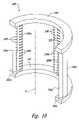
- FIG. 4is an isometric view of a microfeature workpiece holder in accordance with one embodiment of the invention.
- FIG. 5is a side elevation view of the microfeature workpiece holder of FIG. 4 .
- FIG. 6is a schematic cross-sectional view of the microfeature workpiece holder of FIGS. 4 and 5 taken along line 6 — 6 of FIG. 5 .
- FIG. 7is a schematic cross-sectional view of the microfeature workpiece holder of FIGS. 4–6 taken along line 7 — 7 of FIG. 6 .
- FIG. 8is a schematic cross-sectional view of the microfeature workpiece holder of FIGS. 4–7 taken along line 8 — 8 of FIG. 6 .
- FIG. 9is a schematic side elevation view of a microfeature workpiece holder in accordance with another embodiment of the invention.
- FIG. 10is a schematic isometric view of a microfeature workpiece holder in accordance with yet another embodiment of the invention.
- FIG. 11is a schematic side elevation view of the microfeature workpiece holder of FIG. 10 .
- FIG. 12is a schematic cross-sectional view of the microfeature workpiece holder of FIGS. 10 and 11 taken along line 12 — 12 of FIG. 11 .
- FIG. 13is a schematic cross-sectional view of a portion of the microfeature workpiece holder of FIGS. 10–12 taken along line 13 — 13 of FIG. 12 .
- FIG. 14is a schematic cross-sectional view of a portion of microfeature workpiece holder of FIGS. 10–13 taken along line 14 — 14 of FIG. 12 .
- FIG. 15is a schematic illustration of a microfeature workpiece processing system in accordance with a further embodiment of the invention.
- FIG. 16is a schematic illustration of a microfeature workpiece processing system in accordance with another embodiment of the invention.
- FIG. 17is a schematic illustration of a microfeature workpiece processing system in accordance with yet another embodiment of the invention.
- microfeature workpiece holderssystems including processing chambers, and methods for depositing materials onto microfeature workpieces. Many specific details of the invention are described below with reference to reactors for depositing materials onto microfeature workpieces.
- microfeature workpieceis used throughout to include substrates upon which and/or in which microelectronic devices, micromechanical devices, data storage elements, read/write components, and other devices are fabricated.
- microfeature workpiecescan be semiconductor wafers such as silicon or gallium arsenide wafers, glass substrates, insulative substrates, and many other types of materials.
- the microfeature workpiecestypically have submicron features with dimensions of 0.05 microns or greater.
- gasis used throughout to include any form of matter that has no fixed shape and will conform in volume to the space available, which specifically includes vapors (i.e., a gas having a temperature less than the critical temperature so that it may be liquefied or solidified by compression at a constant temperature).
- vaporsi.e., a gas having a temperature less than the critical temperature so that it may be liquefied or solidified by compression at a constant temperature.
- microfeature workpiece holdersthat are adapted to hold a plurality of microfeature workpieces, e.g., for chemical processing such as ALD.
- These workpiece holdersmay include a gas distributor comprising one or more gas delivery conduits.
- the gas delivery conduitmay have an inlet and a plurality of outlets, which may be positioned to direct a flow of process gas into the spaces between the workpieces. This can facilitate more uniform distribution of reaction precursors on a microfeature workpiece surface, for example.
- the distribution of these outletsmay also facilitate rapid and effective purging of the space between the workpieces.
- microfeature workpiece processing systemsmay include an enclosure defining a process chamber, a removable microfeature workpiece holder disposed in the processing chamber, and a process gas supply conduit.
- the workpiece holdermay be similar to the workpiece holders described above and include a gas distributor having outlets adapted to direct a flow of gas from the process gas supply between the microfeature workpieces.
- One method having particular utility in connection with ALDincludes positioning a microfeature workpiece holder in a process chamber, with the microfeature workpiece holder supporting a plurality of workpieces to define process spaces between each pair of adjacent workpieces.
- a first precursor gasmay be delivered to the process chamber to deposit a quantity of the first precursor gas on a surface of each of the microfeature workpieces.
- a purge gasmay be delivered to the microfeature workpiece holder.
- the microfeature workpiece holdermay carry a gas distributor that delivers a first flow of the purge gas transversely into the space between a pair of workpieces and delivers a second flow of the purge gas transversely into a process space between another pair of workpieces.
- the methodmay further include delivering a second precursor gas to the process chamber; the second precursor gas reacts with the quantity of the first precursor gas to form a layer of material on the surfaces of the workpieces.
- the first sectiondiscusses microfeature workpiece holders in accordance with selected embodiments of the invention.
- the second sectiondescribes aspects of microfeature workpiece processing systems in other embodiments of the invention.
- the third sectiondiscusses outlines methods in accordance with other aspects of the invention.
- FIGS. 4–8schematically illustrate a microfeature workpiece holder 100 in accordance with one embodiment of the invention.
- This microfeature workpiece holder 100generally includes a base 110 , a plurality of columns 120 , and a cap 150 .
- the particular embodiment shown in FIGS. 4–8employs 3 columns, namely columns 120 a , 120 b and 120 c .
- the base 110 and the cap 150are each generally semicircular in shape and the columns 120 a–c are spaced approximately 90° from one another so that the two outer columns 120 a and 120 c are generally diametrically opposed to one another. It should be recognized that this is simply one possible embodiment that may be useful in connection with microfeature workpieces that are generally circular in shape.
- more or fewer columns 120may be employed.
- the base 110 and/or the cap 150may take the form of a solid plate or disk or have any other desired shape. In other embodiments, only one of the base 110 or cap 150 is employed. For example, the cap 150 may be omitted and the base 110 may provide the requisite support for the columns 120 .
- Each of the columns 120 in the microfeature workpiece holder 100is generally circular in cross-section.
- the columnsmay have other shapes.
- the columns 120may be generally wedge-shaped, such as those suggested in PCT International Publication No. WO 02/095807 entitled, “Silicon Fixtures Useful for High Temperature Wafer Processing,” the teachings of which are incorporated herein by reference.
- Each of the columns 120includes a plurality of workpiece supports spaced longitudinally along its length.
- these workpiece supportscomprise slots 122 that extend into the body of the column 120 .
- the workpiece holdersmay comprise inwardly-extending fingers, rings, clamps, or other workpiece-supporting structures known in the art, e.g., supports used in semiconductor wafer handling and processing equipment.
- FIGS. 4 and 5show columns with a limited number of slots 122 .
- the columns 120may include fewer or more slots.
- each of the slots 122is adapted to receive an edge portion of one of the microfeature workpieces (as suggested in FIG. 5 ).
- a single slot 122may not be deep enough to receive a sufficient portion of a microfeature workpiece W to support the workpiece W.
- the slots 122 on each of the columns 120 a–care positioned relative to one another to cooperatively support the workpieces W.
- each slot 122may be generally horizontally aligned with a corresponding one of the slots 122 on each of the other two columns 120 . This permits a workpiece W to be supported at three separate peripheral locations to enhance the support of each of the workpieces W.
- the slots 122may support a plurality of microfeature workpieces W in a spaced-apart, generally parallel relationship.
- the spaced-apart relationship of the workpieces Wwill define a process space S between each of the workpieces W.
- the microfeature workpiece holder 100also includes a gas distributor 130 .
- This gas distributor 130includes at least one gas delivery conduit 134 adapted to direct a flow of process gas relative to the workpieces W.
- a single gas delivery conduit 134is employed.
- the gas distributor 130includes a manifold 132 connecting a plurality of gas delivery conduits 134 a–c .
- the manifold 132may comprise an arcuate fluid passageway formed in the arcuate base 110 that provides fluid communication between a gas inlet 140 in the base 110 and each of the gas delivery conduits 134 a–c .
- a separate gas delivery conduit 134is associated with each of the columns 120 .
- a first gas delivery conduit 134 ais carried by the first column 120 a
- a second gas delivery conduit 134 bis carried by a second column 120 b
- a third gas delivery conduit 134 cis carried by the third column 120 c .
- one or more of the columns 120may not include a gas delivery conduit 134 .
- more than one gas delivery conduit 134may be carried by each column 120 .
- the gas delivery conduit 134 bmay comprise an internal lumen formed in the second column 120 b .
- FIGS. 6–8only illustrate the second column 120 b , the structure of the other columns 120 a and 120 c may be substantially the same.
- the following discussiongenerically refers to a column 120 and a gas delivery conduit 134 .
- the gas delivery conduit 134includes a plurality of transverse passages 136 , each of which directs fluid from the gas delivery conduit 134 to one of a plurality of outlets 138 . These outlets 138 are disposed between two adjacent slots 122 .
- the gas delivery conduit 134including each of the transverse passages 136 is generally circular in cross-section and the outlets 138 define generally circular openings.
- the size and shape of the gas delivery conduits 134 and outlets 138 in the microfeature workpiece holder 100can be varied, though.
- the outlets 138may comprise ellipses or slots having a transverse dimension longer than a longitudinal dimension or include a directional nozzle (not shown).
- microfeature workpieces WWhen the microfeature workpieces W are loaded in the microfeature workpiece holder 100 , they will define a series of process spaces S. At least one outlet 138 is desirably associated with each of these process spaces S. In the illustrated embodiment, one outlet 138 is positioned between each pair of adjacent slots 122 on each of the columns 120 a–c . As a consequence, three outlets 138 are associated with each process space, with one outlet being associated with each of the columns 120 a–c supporting the workpieces W. Directing transverse gas flows into the processing spaces S can further enhance the flow of process gas from the gas distributor 130 into and through the processing spaces S.
- each of the outlets 138may be directed inwardly toward a central axis A (in FIG. 4 ) of the microfeature workpiece holder 100 . Consequently, when the workpieces W are positioned in the holder 100 , each of the outlets 138 will be positioned to direct a flow of process gas inwardly toward a center of one of the workpieces W. This is expected to further enhance the uniformity of material deposition and/or decrease the time needed to purge the system.
- the microfeature workpiece holder 100can be formed of any material that is suitable in light of the microfeature workpieces W with which it will be used and the anticipated conditions of use. If the microfeature workpieces W comprise semiconductor wafers, for example, the microfeature workpiece holder 100 may be formed from glass, fused silica (e.g., fused quartz), or polysilicon (i.e., polycrystalline silicon), among other materials. For other types of applications that may be less sensitive to contamination, the microfeature workpiece holder 100 may be formed of a metal, a ceramic, or a suitably stiff and durable polymeric material.
- fused silicae.g., fused quartz
- polysiliconi.e., polycrystalline silicon
- FIG. 9schematically illustrates a microfeature workpiece holder 102 in accordance with another embodiment of the invention.
- This microfeature workpiece holder 102is similar in many respects to the microfeature workpiece holder 100 shown in FIGS. 4–8 and like reference numbers are used in FIGS. 4–9 to illustrate like elements.
- the gas distributor 130 shown in FIG. 5employs a single gas inlet 140 that communicates with each of the gas delivery conduits 134 a–c through a common manifold 132 .
- the microfeature workpiece holder 102 of FIG. 9does not include a manifold 132 . Instead, the gas distributor 131 in FIG. 9 has a separate gas inlet 140 for each of the gas delivery conduits 134 .
- each of the gas delivery conduits 134may be adapted to deliver a process gas flow that is independent of the process gas flow delivered through each of the other conduits 134 . As noted below, this may permit a different process gas to be delivered through each of the conduits 134 a–c .
- ALD processoutlined above in connection with FIGS.
- one of the gas delivery conduitsmay be dedicated to delivering the first precursor gas A
- a second one of the gas delivery conduitse.g., conduit 134 b
- the third gas delivery conduit 134 cmay be used to deliver the purge gas.
- FIGS. 10–14schematically illustrate a microfeature workpiece holder 200 in accordance with another embodiment of the invention.
- This microfeature workpiece holder 200generally includes a base 210 , a cap 250 , and at least one column 220 extending between the base 210 and the cap 250 .
- the illustrated embodimentemploys three columns 220 a – 220 c that are spaced generally equiangularly in a manner similar to that described above in connection with the microfeature workpiece holder 100 of FIG. 4 .
- Each of the columns 220 a–cmay include a series of longitudinally-spaced slots 222 oriented inwardly toward a central axis A of the microfeature workpiece holder 200 .
- Each of these slots 222may be adapted to receive an edge portion of a microfeature workpiece W (omitted in FIGS. 10–14 for ease of understanding).
- Each of the slots 222 in a particular column 220may be positioned relative to a corresponding slot 222 in each of the other columns 220 so the three corresponding slots 222 can cooperatively support a microfeature workpiece W.
- the gas distributor 130includes several gas delivery conduits 134 , each of which comprises an internal lumen of one of the columns 120 .
- the microfeature workpiece holder 200 of FIGS. 10–14in contrast, has substantially solid columns 220 . As suggested in FIGS. 12 and 14 , the columns 220 may have a solid interior with a series of spaced-apart slots 222 formed in an inwardly-oriented surface of the column.
- the microfeature workpiece holder 200also includes a gas distributor, generally designated as reference number 230 , that includes a series of gas delivery conduits 234 .
- a first gas delivery conduit 234 ais carried with respect to the first column 220 a
- a second gas delivery conduit 234 bis carried with respect to a second column 220 b
- a third gas delivery conduit 234 cis carried with respect to a third column 220 c .
- the position of each of the gas delivery conduits 234may be fixed relative to the adjacent column 220 in any desired fashion.
- the gas delivery conduits 234may be supported entirely by the base 210 and/or the cap 250 . In the particular embodiments shown in FIGS.
- each of the conduits 234is received within and passes through an opening in the base 210 , but the opposite end of the gas delivery conduit 234 is spaced from the cap 250 .
- each of the conduits 234is attached to the cap 250 , as well.
- each of the gas delivery conduits 234 in the illustrated embodimentis positioned immediately adjacent to one of the columns 220 .
- each of the conduits 234may be attached to or otherwise physically supported by the adjacent column 220 .
- the conduits 234may be attached only to an adjacent column 220 without being directly attached to the base 210 or the cap 250 .
- the gas delivery conduits 234need not be positioned close to any of the columns 220 .
- one gas delivery conduit 234may be positioned between the first two columns 220 a and 220 b and a second gas delivery conduit 234 may be positioned between the second and third columns 220 b and 220 c.
- the gas delivery conduits 234provide a fluid pathway between a gas inlet 240 and a plurality of gas outlets 238 .
- the gas delivery conduits 234may include a longitudinally extending channel 235 and a series of transverse pathways 236 extending transversely inwardly toward the axis (axis A in FIG. 10 ) of the microfeature workpiece holder 200 .
- the outlets 238 of these pathways 236may be positioned laterally along the length of the respective conduit 234 so each outlet 238 can direct a flow of process gas intermediate a pair of adjacent slots 222 .
- these outlets 238would, therefore, direct a flow of process gas into the process space (S in FIG. 5 ) defined between two adjacent microfeature workpieces W.
- the gas distributor 230 of FIGS. 10–14includes a separate gas inlet 240 for each of the gas delivery conduits 234 .
- two or more of the gas delivery conduits 234may communicate with a common inlet 240 via a manifold (not shown) in the base 210 , similar to the manifold 132 in the microfeature workpiece holder 100 discussed above.
- the microfeature workpiece holders 100 , 102 , and 200may be used for a variety of processes.
- FIGS. 15–17schematically illustrate select microfeature workpiece processing systems that employ microfeature workpiece holders to process a batch of microfeature workpieces simultaneously.
- the microfeature workpiece holders employed in these processing systemsmay, in select embodiments, employ features of the microfeature workpiece holders 100 , 102 , and/or 200 described above.
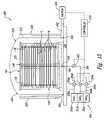
- FIG. 15schematically illustrates a microfeature workpiece processing system 300 in accordance with one embodiment of the invention.
- This system 300includes a reactor 310 adapted to receive a plurality of microfeature workpieces W in a holder.
- the workpieces Ware carried in a workpiece holder 100 substantially as described above in connection with FIGS. 4–8 .
- the reactor 310generally includes an enclosure 320 defined by a wall 322 and a holder-supporting platform 326 .
- the wall 322may sealingly engage the platform 326 , illustrated schematically in FIG. 15 as an O-ring seal 324 . This will define a process chamber 325 within which the microfeature workpiece holder 100 may be received.
- the reactor 310may also include a heater 330 and a vacuum 340 that communicates with the process chamber 325 by a vacuum line 342 .
- the heater 330may be of any conventional design, e.g., an inductance heater or the like.
- a gas supply system 350 of the reactor 310generally includes a plurality of individual gas supplies 352 , with at least one gas supply 352 provided for each of the process gases used in processing workpieces W in the system 300 .
- the illustrated embodimentincludes a first gas supply 352 a to deliver a first gas (GAS 1 ), a second gas supply 352 b adapted to deliver a second gas (GAS 2 ), and a third gas supply 352 c adapted to deliver a third gas (GAS 3 ).
- ALDALD
- the first gas supply 352 amay provide a supply of the first precursor A
- the second gas supply 352 bmay provide a supply of the second precursor B
- the third gas supply 352 cmay provide a supply of the purge gas.
- Each of the individual gas supplies 352 a–cmay be provided with an individual gas supply line 356 a–c , respectively. These individual supply lines 356 a–c are coupled to a primary gas supply line 356 .
- each of the individual gas supply lines 356 a–cis provided with a selectively controllable secondary valve 354 a–c , respectively. These secondary valves may be used to control the flow rate of the gas from each of the individual gas supply 352 into the main gas supply line 356 , hence regulating the composition and flow rate of gas to the gas supply line 356 .
- the gas distributor 130 of the holder 100may be coupled to the gas supply system 350 in a variety of manners.
- a gas fitting 360 in the platform 326may be releasably coupled to the gas inlet 140 of the holder 100 .
- This fitting 360is coupled to the remainder of the gas supply 350 by a supply line 356 .
- the flow of gas through the supply line 356 to the gas distributor 130 of the holder 100may be controlled, at least in part, by a main valve 362 that is under the control of a controller 370 .
- the controller 370may take any of a variety of forms.
- the controller 370comprises a computer having a programmable processor programmed to control operation of the system 300 to deposit material on the workpieces W.
- the controller 370may also be operatively coupled to the secondary valves 354 a–c to control the composition of the gas delivered to the main valve 362 via the supply line 356 .
- the controller 370may also be coupled to the vacuum 340 (as illustrated) or any other component of the processing system 300 , e.g., the heater 330 .
- FIG. 16schematically illustrates a microfeature workpiece processing system 302 in accordance with an alternative embodiment of the invention.
- This processing system 302is similar in many respects to the processing system 300 of FIG. 15 and like reference numbers are used in FIGS. 15 and 16 to indicate like elements.
- the processing system 300uses the microfeature workpiece holder 100 of FIGS. 4–8 .
- the workpieces W in processing system 302 of FIG. 16are instead held in the microfeature workpiece holder 102 of FIG. 9 .
- the gas distributor 131 of this holder 102has a series of independent gas delivery conduits 134 , each of which has a separate gas inlet 140 .
- the gas supply 351 of FIG. 16is similar in many respects to the gas supply 350 of FIG. 15 .
- each of the individual gas supply lines 356 a–cwere joined into a main supply line 356 for delivery to a single gas fitting 360 .
- each of the individual gas supplies 352 a–cis independently coupled to a separate gas fitting 360 a–c , respectively.
- a first gas fitting 360 amay releasably couple the first gas supply line 356 a to the first inlet 140 a
- a second gas fitting 360 bmay releasably couple a second gas supply line 356 b to the second gas inlet 140 b
- a third gas fitting 360 cmay releasably couple a third gas supply line 356 c to the third gas inlet 140 c .
- the flow of gas from each of the gas supplies 352 a–cmay be independently controlled by a separate valve 354 a–c through a common controller 370 .
- each of the process gases through an independent, dedicated gas delivery conduit 134can avoid the need to purge the gas delivery conduit 134 after delivering one precursor and before delivering another precursor. This may be advantageous in CVD applications because it permits the precursor gases to be introduced separately into the process chamber 325 , more effectively restricting the deposition of the reactant to the vicinity of the workpieces W.
- FIG. 17illustrates a microfeature workpiece processing system 400 in accordance with still another embodiment of the invention.
- This processing system 400generally includes a reactor 410 having a processing enclosure 420 within which a workpiece holder (e.g., workpiece holder 100 of FIGS. 4–8 ) carrying one or more workpieces W may be received.
- the processing enclosure 420is generally defined by an outer wall 422 and a platform 426 adapted to carry the workpiece holder 100 .
- This processing enclosure 420also includes a liner 424 that functionally divides the process chamber 425 into a main chamber 427 and a generally annular exhaust 428 coupled to the vacuum 440 by a vacuum line 442 .
- the reactor 410may also include a heater 430 .
- the processing system 400may include a first gas supply system 450 and a second gas supply system 460 .
- the first gas supply system 450includes a plurality of individual gas supplies 452 a–c , each of which may include a separate process gas.
- the first gas supply 452 amay include a precursor gas A (GAS 1 ) and a second gas supply 452 b may provide a supply of a second precursor gas B (GAS 2 ).
- the first gas supply system 450may also include a supply of a purge gas (GAS 3 ) in a third gas supply.
- Each of these individual gas supplies 452 a–cmay be coupled to a common gas supply line 456 .
- a separate valve 454 a , 454 b , or 454 cmay be operated by a controller 470 to control the flow of gas from the individual gas supplies 452 a , 452 b , and 452 c , respectively.
- the gas supply line 456 of the first gas supply system 450may be in fluid communication with one or more gas supply nozzles 458 .
- the gas supply nozzle 458may be adapted to deliver a flow of process gas to the main chamber 427 outside the process spaces S of the process chamber 425 . This gas may flow generally longitudinally through the main chamber 427 then out of the process chamber 425 via the annular exhaust 428 .
- This gas supply system 450is, in some respects, analogous to the gas supply 30 and gas nozzle 32 illustrated in FIG. 3 .
- the microfeature workpiece processing system 400also includes a second gas supply system 460 .
- This gas supply system 460may be adapted to deliver one or more process gases to the process chamber 425 via the gas distributor 130 of the workpiece holder 100 . Gas will exit the outlets 138 of the gas distributor 130 in a direction transverse to the longitudinally directed flow from the nozzle 458 .
- the second gas supply system 460includes a single individual gas supply 462 containing a purge gas (GAS 3 ).
- the individual gas supply 462is coupled to a gas fitting 468 in the platform 426 by a valve 464 operatively linked to the controller 470 .
- the gas fitting 468is adapted to be releasably coupled to the inlet 140 of the gas distributor 130 .
- the second gas supply system 460 shown in FIG. 16only provides a supply of a single purge gas, this gas supply system 460 may include two or more individual gas supplies 462 to provide a variety of different process gas compositions to the gas distributor 130 .
- FIGS. 15–17the particular microfeature workpiece processing systems 300 , 302 , and 400 shown in FIGS. 15–17 . It should be understood, though, that reference to these particular processing systems and the workpiece holders used therein is solely for purposes of illustration and that the methods outlined below are not limited to any particular workpiece holder or processing system shown in the drawings or discussed in detail above. In addition, the following discussion focuses primarily on ALD and also touches on possible CVD applications. It should be recognized that the processes outlined below should not be limited to these specific deposition processes. Indeed, aspects of the methods outlined below may have utility in applications in which a process other than material deposition, e.g., selective etching, may be carried out.
- a process other than material depositione.g., selective etching
- a method of processing microfeature workpiecesmay include positioning a microfeature workpiece holder 100 in a process chamber 325 (using the processing system 300 as an example).
- the workpiece holder 100may support a plurality of workpieces W in a spaced-apart relationship to define a process space S between each pair of adjacent workpieces W.
- the microfeature workpiece holder 100may be positioned in the process chamber by placing the holder 100 on a platform 326 .
- the gas fitting 360may be coupled to the gas inlet 140 of the gas distributor 130 at this time. Once the holder 100 is in place on the platform 326 , the platform 326 may be moved toward the wall 322 until the seals 324 substantially seal the enclosure 320 to define the process chamber 325 .
- This embodimentalso includes delivering at least a first process gas and a second process gas to the process chamber 325 .
- the first process gase.g., a first precursor A
- the first process gasmay be delivered to the process chamber 325 by opening the first regulator valve 354 a and the main valve 362 . This will allow the first gas to flow into the gas distributor 130 and outwardly into the process chamber 325 via the outlets 138 . As noted above, these outlets 138 will deliver a flow of the process gas transversely into the process spaces S between the workpieces W.
- the second process gasmay be delivered to the process chamber 325 either simultaneously with delivery of the first process gas (e.g., for CVD) or at a different time.
- a flow of the first precursor gas A from the first supply 352 amay be terminated by closing the valve 354 a .
- a flow of purge gas from the third gas supply 352 cmay be delivered into the process spaces S by opening the associated regulator valve 154 c .
- the regulator valve 154 cmay be closed and a flow of the second precursor gas B from the second gas supply 352 b may then be introduced via the nozzles 138 .
- the controller 370may be used to deposit a reaction product via an ALD process such as that discussed above in connection with FIGS. 1 and 2 .
- Delivering process gases transversely into the process space S between the workpieces W via the outlets 138can fairly rapidly change the gas present in the process space S.
- one of the primary mechanisms for gas exchange in the spaces between the workpieces Wis diffusion.
- Delivering a transverse flow of gas in accordance with embodiments of the present inventioncan deliver a more uniform application of the precursors to be chemisorbed or reacted on the surface of the workpiece W.
- Delivering the purge gas through the outlets 138will also provide a more active scrubbing of the gas in the process spaces S, helping clear the process spaces S of any excess precursor gas fairly quickly. This can materially speed up the purge phases of the process illustrated in FIG. 2 .
- the processing system 300 of FIG. 15introduces process gases through a single inlet 140 and the gas distributor 130 of the workpiece holder 100 .
- the processing system 302 of FIG. 16allows each of the process gases (gas 1-3 ) to be introduced into the process chamber 325 through a separate gas delivery conduit 134 a , 134 b , or 134 c .
- Thiscan be particularly useful in both ALD and CVD applications.
- By separating the pathways for delivery of the reaction precursors into separate conduits 134less care need be taken to purge the gas delivery system of the first precursor before introducing a second precursor through the same gas delivery system.
- the gascan be introduced separately and allowed to mix in the process space S and react in the immediate vicinity of the workpiece W. This may facilitate use of more highly reactive precursors, which may be problematic if the precursors are introduced together through a common gas delivery path.
- one of the process gasesmay be introduced through the gas distributor 130 of the workpiece holder 100 , but the second process gas may be delivered through a delivery conduit independent of the gas distributor 130 .
- the precursor gasesmay be introduced from separate individual gas supplies 452 a and 452 b through the gas delivery nozzle 458 . This will deliver the precursors to the process spaces S between the workpieces W in a fashion analogous to that in the ALD reactor 10 of FIG. 3 .
- the purge gasgas 3
- Delivering the purge gas through the outlets 138 of the workpiece holder gas distributor 130will help positively scrub the processing spaces S, fairly rapidly sweeping away any excess precursor.
Landscapes
- Chemical & Material Sciences (AREA)
- General Chemical & Material Sciences (AREA)
- Chemical Kinetics & Catalysis (AREA)
- Engineering & Computer Science (AREA)
- Materials Engineering (AREA)
- Mechanical Engineering (AREA)
- Metallurgy (AREA)
- Organic Chemistry (AREA)
- Chemical Vapour Deposition (AREA)
- Container, Conveyance, Adherence, Positioning, Of Wafer (AREA)
- Crystals, And After-Treatments Of Crystals (AREA)
- Inorganic Insulating Materials (AREA)
Abstract
Description
The present invention is related to equipment and methods for processing microfeature workpieces, e.g., semiconductor wafers. Aspects of the invention have particular utility in connection with batch deposition of materials on microfeature workpieces, such as by atomic layer deposition or chemical vapor deposition.
Thin film deposition techniques are widely used in the manufacturing of microfeatures to form a coating on a workpiece that closely conforms to the surface topography. In the context of microelectronic components, for example, the size of the individual components in the devices on a wafer is constantly decreasing, and the number of layers in the devices is increasing. As a result, the density of components and the aspect ratios of depressions (e.g., the ratio of the depth to the size of the opening) are increasing. The size of such wafers is also increasing to provide more real estate for forming more dies (i.e., chips) on a single wafer. Many fabricators are currently transitioning from 200 mm to 300 mm workpieces, and even larger workpieces will likely be used in the future. Thin film deposition techniques accordingly strive to produce highly uniform conformal layers that cover the sidewalls, bottoms, and corners in deep depressions that have very small openings.
One widely used thin film deposition technique is chemical vapor deposition (CVD). In a CVD system, one or more precursors that are capable of reacting to form a solid thin film are mixed in a gas or vapor state, and then the precursor mixture is presented to the surface of the workpiece. The surface of the workpiece catalyzes the reaction between the precursors to form a solid thin film at the workpiece surface. A common way to catalyze the reaction at the surface of the workpiece is to heat the workpiece to a temperature that causes the reaction.
Although CVD techniques are useful in many applications, they also have several drawbacks. For example, if the precursors are not highly reactive, then a high workpiece temperature is needed to achieve a reasonable deposition rate. Such high temperatures are not typically desirable because heating the workpiece can be detrimental to the structures and other materials already formed on the workpiece. Implanted or doped materials, for example, can migrate within silicon workpieces at higher temperatures. On the other hand, if more reactive precursors are used so that the workpiece temperature can be lower, then reactions may occur prematurely in the gas phase before reaching the intended surface of the workpiece. This is undesirable because the film quality and uniformity may suffer, and also because it limits the types of precursors that can be used.
Atomic layer deposition (ALD) is another thin film deposition technique.FIGS. 1A and 1B schematically illustrate the basic operation of ALD processes. Referring toFIG. 1A , a layer of gas molecules A coats the surface of a workpiece W. The layer of A molecules is formed by exposing the workpiece W to a precursor gas containing A molecules, and then purging the chamber with a purge gas to remove excess A molecules. This process can form a monolayer of A molecules on the surface of the workpiece W because the A molecules at the surface are held in place during the purge cycle by physical adsorption forces at moderate temperatures or chemisorption forces at higher temperatures. The layer of A molecules is then exposed to another precursor gas containing B molecules. The A molecules react with the B molecules to form an extremely thin layer of solid material C on the workpiece W. The chamber is then purged again with a purge gas to remove excess B molecules.
One drawback of ALD processing is that it has a relatively low throughput compared to CVD techniques. For example, ALD processing typically takes several seconds to perform each A-purge-B-purge cycle. This results in a total process time of several minutes to form a single thin layer of only 60 Å. In contrast to ALD processing, CVD techniques only require about one minute to form a 60 Å thick layer. In single-wafer processing chambers, ALD processes can be 500%–2000% longer than corresponding single-wafer CVD processes. The low throughput of existing single-wafer ALD techniques limits the utility of the technology in its current state because ALD may be a bottleneck in the overall manufacturing process.
One promising solution to increase the throughput of ALD processing is processing a plurality of wafers (e.g., 20–250) simultaneously in a batch process.FIG. 3 schematically illustrates a conventionalbatch ALD reactor 10 having aprocessing enclosure 20 coupled to agas supply 30 and avacuum 40. Theprocessing enclosure 20 generally includes anouter wall 22 and anannular liner 24. Aplatform 60 seals against the outer wall or some other part of theenclosure 20 via aseal 62 to define aprocess chamber 25. Gas is introduced from thegas supply 30 to theprocess chamber 25 by agas nozzle 32 that introduces gas into themain chamber 28 of theprocess chamber 25. Under influence of thevacuum 40, the gas introduced via thegas nozzle 32 will flow through themain chamber 28 and outwardly into theannular exhaust 26 to be drawn out with avacuum 40. A plurality of workpieces W, e.g., semiconductor wafers, may be held in the processing enclosure in aworkpiece holder 70. In operation, aheater 50 heats the workpieces W to a desired temperature and thegas supply 30 delivers the first precursor A, the purge gas, and the second precursor B as discussed above in connection withFIG. 2 .
However, when depositing material simultaneously on a large number of workpieces in anALD reactor 10 such as that shown inFIG. 3 , it can be difficult to uniformly deposit the precursors A and B across the surface of each of the workpieces W. Removing excess precursor from the spaces between the workpieces W can also be problematic. In an ALD reactor such as that shown inFIG. 3 , the primary mechanism for removing residual precursor that is not chemisorbed on the surface of one of the workpieces is diffusion. This is not only a relatively slow process that significantly reduces the throughput of thereactor 10, but it also may not adequately remove residual precursor. As such, conventional batch ALD reactors may have a low throughput and form non-uniform films.
A. Overview
Various embodiments of the present invention provide microfeature workpiece holders, systems including processing chambers, and methods for depositing materials onto microfeature workpieces. Many specific details of the invention are described below with reference to reactors for depositing materials onto microfeature workpieces. The term “microfeature workpiece” is used throughout to include substrates upon which and/or in which microelectronic devices, micromechanical devices, data storage elements, read/write components, and other devices are fabricated. For example, microfeature workpieces can be semiconductor wafers such as silicon or gallium arsenide wafers, glass substrates, insulative substrates, and many other types of materials. The microfeature workpieces typically have submicron features with dimensions of 0.05 microns or greater. Furthermore, the term “gas” is used throughout to include any form of matter that has no fixed shape and will conform in volume to the space available, which specifically includes vapors (i.e., a gas having a temperature less than the critical temperature so that it may be liquefied or solidified by compression at a constant temperature). Several embodiments in accordance with the invention are set forth inFIGS. 4–17 and the following text to provide a thorough understanding of particular embodiments of the invention. A person skilled in the art will understand, however, that the invention may have additional embodiments, or that the invention may be practiced without several of the details of the embodiments shown inFIGS. 4–17 .
Certain embodiments of the invention provide microfeature workpiece holders that are adapted to hold a plurality of microfeature workpieces, e.g., for chemical processing such as ALD. These workpiece holders may include a gas distributor comprising one or more gas delivery conduits. The gas delivery conduit may have an inlet and a plurality of outlets, which may be positioned to direct a flow of process gas into the spaces between the workpieces. This can facilitate more uniform distribution of reaction precursors on a microfeature workpiece surface, for example. The distribution of these outlets may also facilitate rapid and effective purging of the space between the workpieces.
Other embodiments of the invention provide microfeature workpiece processing systems that may include an enclosure defining a process chamber, a removable microfeature workpiece holder disposed in the processing chamber, and a process gas supply conduit. The workpiece holder may be similar to the workpiece holders described above and include a gas distributor having outlets adapted to direct a flow of gas from the process gas supply between the microfeature workpieces.
Other embodiments of the invention provide methods of depositing materials on microfeature workpieces. Although a number of methods are described below, one method having particular utility in connection with ALD includes positioning a microfeature workpiece holder in a process chamber, with the microfeature workpiece holder supporting a plurality of workpieces to define process spaces between each pair of adjacent workpieces. A first precursor gas may be delivered to the process chamber to deposit a quantity of the first precursor gas on a surface of each of the microfeature workpieces. A purge gas may be delivered to the microfeature workpiece holder. The microfeature workpiece holder may carry a gas distributor that delivers a first flow of the purge gas transversely into the space between a pair of workpieces and delivers a second flow of the purge gas transversely into a process space between another pair of workpieces. The method may further include delivering a second precursor gas to the process chamber; the second precursor gas reacts with the quantity of the first precursor gas to form a layer of material on the surfaces of the workpieces.
For ease of understanding, the following discussion is subdivided into three areas of emphasis. The first section discusses microfeature workpiece holders in accordance with selected embodiments of the invention. The second section describes aspects of microfeature workpiece processing systems in other embodiments of the invention. The third section discusses outlines methods in accordance with other aspects of the invention.
B. Microfeature Workpiece Holders
Each of the columns120 in themicrofeature workpiece holder 100 is generally circular in cross-section. In other embodiments, the columns may have other shapes. For example, the columns120 may be generally wedge-shaped, such as those suggested in PCT International Publication No. WO 02/095807 entitled, “Silicon Fixtures Useful for High Temperature Wafer Processing,” the teachings of which are incorporated herein by reference.
Each of the columns120 includes a plurality of workpiece supports spaced longitudinally along its length. In the illustrated embodiment, these workpiece supports compriseslots 122 that extend into the body of the column120. In other embodiments, the workpiece holders may comprise inwardly-extending fingers, rings, clamps, or other workpiece-supporting structures known in the art, e.g., supports used in semiconductor wafer handling and processing equipment.FIGS. 4 and 5 show columns with a limited number ofslots 122. Depending on the application in which theworkpiece holder 100 is used, the columns120 may include fewer or more slots.
The size and shape of theslots 122 can be modified as desired. In one embodiment, each of theslots 122 is adapted to receive an edge portion of one of the microfeature workpieces (as suggested inFIG. 5 ). Asingle slot 122 may not be deep enough to receive a sufficient portion of a microfeature workpiece W to support the workpiece W. In the illustrated embodiment, theslots 122 on each of thecolumns 120a–care positioned relative to one another to cooperatively support the workpieces W. As illustrated inFIG. 5 , eachslot 122 may be generally horizontally aligned with a corresponding one of theslots 122 on each of the other two columns120. This permits a workpiece W to be supported at three separate peripheral locations to enhance the support of each of the workpieces W. If theseslots 122 are spaced the same distance along the length of each of the columns120, theslots 122 may support a plurality of microfeature workpieces W in a spaced-apart, generally parallel relationship. The spaced-apart relationship of the workpieces W will define a process space S between each of the workpieces W.
As shown schematically inFIG. 5 , themicrofeature workpiece holder 100 also includes agas distributor 130. Thisgas distributor 130 includes at least onegas delivery conduit 134 adapted to direct a flow of process gas relative to the workpieces W. In one embodiment, a singlegas delivery conduit 134 is employed. In the particular embodiment shown schematically inFIG. 5 , thegas distributor 130 includes a manifold132 connecting a plurality ofgas delivery conduits 134a–c. The manifold132 may comprise an arcuate fluid passageway formed in thearcuate base 110 that provides fluid communication between agas inlet 140 in thebase 110 and each of thegas delivery conduits 134a–c. In the illustrated embodiment, a separategas delivery conduit 134 is associated with each of the columns120. Hence, a firstgas delivery conduit 134ais carried by thefirst column 120a, a secondgas delivery conduit 134bis carried by asecond column 120b, and a thirdgas delivery conduit 134cis carried by thethird column 120c. In some embodiments, one or more of the columns120 may not include agas delivery conduit 134. In other embodiments, more than onegas delivery conduit 134 may be carried by each column120.
As best seen inFIGS. 6–8 , thegas delivery conduit 134bmay comprise an internal lumen formed in thesecond column 120b. (AlthoughFIGS. 6–8 only illustrate thesecond column 120b, the structure of theother columns gas delivery conduit 134.) Thegas delivery conduit 134 includes a plurality oftransverse passages 136, each of which directs fluid from thegas delivery conduit 134 to one of a plurality ofoutlets 138. Theseoutlets 138 are disposed between twoadjacent slots 122. Thegas delivery conduit 134, including each of thetransverse passages 136 is generally circular in cross-section and theoutlets 138 define generally circular openings. The size and shape of thegas delivery conduits 134 andoutlets 138 in themicrofeature workpiece holder 100 can be varied, though. In other embodiments, for example, theoutlets 138 may comprise ellipses or slots having a transverse dimension longer than a longitudinal dimension or include a directional nozzle (not shown).
When the microfeature workpieces W are loaded in themicrofeature workpiece holder 100, they will define a series of process spaces S. At least oneoutlet 138 is desirably associated with each of these process spaces S. In the illustrated embodiment, oneoutlet 138 is positioned between each pair ofadjacent slots 122 on each of thecolumns 120a–c. As a consequence, threeoutlets 138 are associated with each process space, with one outlet being associated with each of thecolumns 120a–csupporting the workpieces W. Directing transverse gas flows into the processing spaces S can further enhance the flow of process gas from thegas distributor 130 into and through the processing spaces S.
Referring back toFIG. 4 , each of theoutlets 138 may be directed inwardly toward a central axis A (inFIG. 4 ) of themicrofeature workpiece holder 100. Consequently, when the workpieces W are positioned in theholder 100, each of theoutlets 138 will be positioned to direct a flow of process gas inwardly toward a center of one of the workpieces W. This is expected to further enhance the uniformity of material deposition and/or decrease the time needed to purge the system.
Themicrofeature workpiece holder 100 can be formed of any material that is suitable in light of the microfeature workpieces W with which it will be used and the anticipated conditions of use. If the microfeature workpieces W comprise semiconductor wafers, for example, themicrofeature workpiece holder 100 may be formed from glass, fused silica (e.g., fused quartz), or polysilicon (i.e., polycrystalline silicon), among other materials. For other types of applications that may be less sensitive to contamination, themicrofeature workpiece holder 100 may be formed of a metal, a ceramic, or a suitably stiff and durable polymeric material.
One difference between themicrofeature workpiece holders gas distributor 130 shown inFIG. 5 employs asingle gas inlet 140 that communicates with each of thegas delivery conduits 134a–cthrough acommon manifold 132. Themicrofeature workpiece holder 102 ofFIG. 9 does not include amanifold 132. Instead, thegas distributor 131 inFIG. 9 has aseparate gas inlet 140 for each of thegas delivery conduits 134. Hence, oneinlet 140ais in fluid communication with a first one of thegas delivery conduits 134a, asecond gas inlet 140bis in fluid communication with a secondgas delivery conduit 134b, and athird gas inlet 140cis in fluid communication with a thirdgas delivery conduit 134c. In this design, each of thegas delivery conduits 134 may be adapted to deliver a process gas flow that is independent of the process gas flow delivered through each of theother conduits 134. As noted below, this may permit a different process gas to be delivered through each of theconduits 134a–c. In the context of the ALD process outlined above in connection withFIGS. 1 and 2 , for example, one of the gas delivery conduits (e.g.,conduit 134a) may be dedicated to delivering the first precursor gas A, a second one of the gas delivery conduits (e.g.,conduit 134b) may be used to deliver the second precursor gas B, and the thirdgas delivery conduit 134cmay be used to deliver the purge gas.
One of the differences between themicrofeature workpiece holders FIGS. 4–8 and10–14, respectively, relates to the relationship of the gas distributor to the columns of the workpiece holder. In theworkpiece holder 100 ofFIGS. 4–8 , thegas distributor 130 includes severalgas delivery conduits 134, each of which comprises an internal lumen of one of the columns120. Themicrofeature workpiece holder 200 ofFIGS. 10–14 , in contrast, has substantiallysolid columns 220. As suggested inFIGS. 12 and 14 , thecolumns 220 may have a solid interior with a series of spaced-apartslots 222 formed in an inwardly-oriented surface of the column.
Referring toFIG. 11 , themicrofeature workpiece holder 200 also includes a gas distributor, generally designated asreference number 230, that includes a series of gas delivery conduits234. In particular, a firstgas delivery conduit 234ais carried with respect to thefirst column 220a, a secondgas delivery conduit 234bis carried with respect to asecond column 220b, and a thirdgas delivery conduit 234cis carried with respect to athird column 220c. The position of each of the gas delivery conduits234 may be fixed relative to theadjacent column 220 in any desired fashion. In one embodiment, the gas delivery conduits234 may be supported entirely by thebase 210 and/or thecap 250. In the particular embodiments shown inFIGS. 10 and 11 , abase portion 242 of each of the conduits234 is received within and passes through an opening in thebase 210, but the opposite end of the gas delivery conduit234 is spaced from thecap 250. In another embodiment, each of the conduits234 is attached to thecap 250, as well. As shown inFIGS. 11 and 12 , each of the gas delivery conduits234 in the illustrated embodiment is positioned immediately adjacent to one of thecolumns 220. In such an arrangement, each of the conduits234 may be attached to or otherwise physically supported by theadjacent column 220. In other embodiments (not shown), the conduits234 may be attached only to anadjacent column 220 without being directly attached to the base210 or thecap 250. In still other embodiments, the gas delivery conduits234 need not be positioned close to any of thecolumns 220. For example, one gas delivery conduit234 may be positioned between the first twocolumns third columns
The gas delivery conduits234 provide a fluid pathway between agas inlet 240 and a plurality ofgas outlets 238. As illustrated inFIG. 13 , the gas delivery conduits234 (in this case,gas delivery conduit 234b) may include alongitudinally extending channel 235 and a series oftransverse pathways 236 extending transversely inwardly toward the axis (axis A inFIG. 10 ) of themicrofeature workpiece holder 200. Theoutlets 238 of thesepathways 236 may be positioned laterally along the length of the respective conduit234 so eachoutlet 238 can direct a flow of process gas intermediate a pair ofadjacent slots 222. When the microfeature workpieces W (not shown inFIGS. 10 and 11 ) are positioned in themicrofeature workpiece holder 200, theseoutlets 238 would, therefore, direct a flow of process gas into the process space (S inFIG. 5 ) defined between two adjacent microfeature workpieces W.
Thegas distributor 230 ofFIGS. 10–14 includes aseparate gas inlet 240 for each of the gas delivery conduits234. In an alternative embodiment, two or more of the gas delivery conduits234 may communicate with acommon inlet 240 via a manifold (not shown) in thebase 210, similar to the manifold132 in themicrofeature workpiece holder 100 discussed above.
C. Microfeature Workpiece Processing Systems
Themicrofeature workpiece holders FIGS. 15–17 schematically illustrate select microfeature workpiece processing systems that employ microfeature workpiece holders to process a batch of microfeature workpieces simultaneously. The microfeature workpiece holders employed in these processing systems may, in select embodiments, employ features of themicrofeature workpiece holders
Thereactor 310 generally includes anenclosure 320 defined by awall 322 and a holder-supportingplatform 326. Thewall 322 may sealingly engage theplatform 326, illustrated schematically inFIG. 15 as an O-ring seal 324. This will define aprocess chamber 325 within which themicrofeature workpiece holder 100 may be received. Thereactor 310 may also include aheater 330 and avacuum 340 that communicates with theprocess chamber 325 by avacuum line 342. Theheater 330 may be of any conventional design, e.g., an inductance heater or the like.
Agas supply system 350 of thereactor 310 generally includes a plurality of individual gas supplies352, with at least one gas supply352 provided for each of the process gases used in processing workpieces W in thesystem 300. The illustrated embodiment includes afirst gas supply 352ato deliver a first gas (GAS1), asecond gas supply 352badapted to deliver a second gas (GAS2), and athird gas supply 352cadapted to deliver a third gas (GAS3). In the context of ALD such as that discussed above in connection withFIGS. 1 and 2 , thefirst gas supply 352amay provide a supply of the first precursor A, thesecond gas supply 352bmay provide a supply of the second precursor B, and thethird gas supply 352cmay provide a supply of the purge gas. Each of the individual gas supplies352a–cmay be provided with an individualgas supply line 356a–c, respectively. Theseindividual supply lines 356a–care coupled to a primarygas supply line 356. In the illustrated embodiment, each of the individualgas supply lines 356a–cis provided with a selectively controllablesecondary valve 354a–c, respectively. These secondary valves may be used to control the flow rate of the gas from each of the individual gas supply352 into the maingas supply line 356, hence regulating the composition and flow rate of gas to thegas supply line 356.
Thegas distributor 130 of theholder 100 may be coupled to thegas supply system 350 in a variety of manners. In the schematic illustration ofFIG. 15 , a gas fitting360 in theplatform 326 may be releasably coupled to thegas inlet 140 of theholder 100. This fitting360 is coupled to the remainder of thegas supply 350 by asupply line 356.
The flow of gas through thesupply line 356 to thegas distributor 130 of theholder 100 may be controlled, at least in part, by amain valve 362 that is under the control of acontroller 370. Thecontroller 370 may take any of a variety of forms. In one embodiment, thecontroller 370 comprises a computer having a programmable processor programmed to control operation of thesystem 300 to deposit material on the workpieces W. Thecontroller 370 may also be operatively coupled to thesecondary valves 354a–cto control the composition of the gas delivered to themain valve 362 via thesupply line 356. Thecontroller 370 may also be coupled to the vacuum340 (as illustrated) or any other component of theprocessing system 300, e.g., theheater 330.
Thegas supply 351 ofFIG. 16 is similar in many respects to thegas supply 350 ofFIG. 15 . InFIG. 15 , each of the individualgas supply lines 356a–cwere joined into amain supply line 356 for delivery to asingle gas fitting 360. In thegas supply 351 ofFIG. 16 , however, each of the individual gas supplies352a–cis independently coupled to a separate gas fitting360a–c, respectively. In particular, a first gas fitting360amay releasably couple the firstgas supply line 356ato thefirst inlet 140a, a second gas fitting360bmay releasably couple a secondgas supply line 356bto thesecond gas inlet 140b, and a third gas fitting360cmay releasably couple a thirdgas supply line 356cto thethird gas inlet 140c. The flow of gas from each of the gas supplies352a–cmay be independently controlled by aseparate valve 354a–cthrough acommon controller 370. Introducing each of the process gases through an independent, dedicatedgas delivery conduit 134 can avoid the need to purge thegas delivery conduit 134 after delivering one precursor and before delivering another precursor. This may be advantageous in CVD applications because it permits the precursor gases to be introduced separately into theprocess chamber 325, more effectively restricting the deposition of the reactant to the vicinity of the workpieces W.
Theprocessing system 400 may include a firstgas supply system 450 and a secondgas supply system 460. The firstgas supply system 450 includes a plurality of individual gas supplies452a–c, each of which may include a separate process gas. Hence, thefirst gas supply 452amay include a precursor gas A (GAS1) and asecond gas supply 452bmay provide a supply of a second precursor gas B (GAS2). Optionally, the firstgas supply system 450 may also include a supply of a purge gas (GAS3) in a third gas supply. Each of these individual gas supplies452a–cmay be coupled to a commongas supply line 456. Aseparate valve controller 470 to control the flow of gas from the individual gas supplies452a,452b, and452c, respectively.
Thegas supply line 456 of the firstgas supply system 450 may be in fluid communication with one or moregas supply nozzles 458. Thegas supply nozzle 458 may be adapted to deliver a flow of process gas to themain chamber 427 outside the process spaces S of theprocess chamber 425. This gas may flow generally longitudinally through themain chamber 427 then out of theprocess chamber 425 via theannular exhaust 428. Thisgas supply system 450 is, in some respects, analogous to thegas supply 30 andgas nozzle 32 illustrated inFIG. 3 .
The microfeatureworkpiece processing system 400 also includes a secondgas supply system 460. Thisgas supply system 460 may be adapted to deliver one or more process gases to theprocess chamber 425 via thegas distributor 130 of theworkpiece holder 100. Gas will exit theoutlets 138 of thegas distributor 130 in a direction transverse to the longitudinally directed flow from thenozzle 458. In the specific embodiment shown inFIG. 17 , the secondgas supply system 460 includes a singleindividual gas supply 462 containing a purge gas (GAS3). Theindividual gas supply 462 is coupled to a gas fitting468 in theplatform 426 by avalve 464 operatively linked to thecontroller 470. Thegas fitting 468 is adapted to be releasably coupled to theinlet 140 of thegas distributor 130. Although the secondgas supply system 460 shown inFIG. 16 only provides a supply of a single purge gas, thisgas supply system 460 may include two or more individual gas supplies462 to provide a variety of different process gas compositions to thegas distributor 130.
D. Methods of Depositing Materials On Microfeature Workpieces
As noted above, other embodiments of the invention provide methods of processing microfeature workpieces. In the following discussion, reference is made to the particular microfeatureworkpiece processing systems FIGS. 15–17 . It should be understood, though, that reference to these particular processing systems and the workpiece holders used therein is solely for purposes of illustration and that the methods outlined below are not limited to any particular workpiece holder or processing system shown in the drawings or discussed in detail above. In addition, the following discussion focuses primarily on ALD and also touches on possible CVD applications. It should be recognized that the processes outlined below should not be limited to these specific deposition processes. Indeed, aspects of the methods outlined below may have utility in applications in which a process other than material deposition, e.g., selective etching, may be carried out.
In accordance with one embodiment, a method of processing microfeature workpieces may include positioning amicrofeature workpiece holder 100 in a process chamber325 (using theprocessing system 300 as an example). Theworkpiece holder 100 may support a plurality of workpieces W in a spaced-apart relationship to define a process space S between each pair of adjacent workpieces W. Themicrofeature workpiece holder 100 may be positioned in the process chamber by placing theholder 100 on aplatform 326. In one embodiment, the gas fitting360 may be coupled to thegas inlet 140 of thegas distributor 130 at this time. Once theholder 100 is in place on theplatform 326, theplatform 326 may be moved toward thewall 322 until theseals 324 substantially seal theenclosure 320 to define theprocess chamber 325.
This embodiment also includes delivering at least a first process gas and a second process gas to theprocess chamber 325. In one embodiment, the first process gas, e.g., a first precursor A, may be delivered to theprocess chamber 325 by opening thefirst regulator valve 354aand themain valve 362. This will allow the first gas to flow into thegas distributor 130 and outwardly into theprocess chamber 325 via theoutlets 138. As noted above, theseoutlets 138 will deliver a flow of the process gas transversely into the process spaces S between the workpieces W.
The second process gas may be delivered to theprocess chamber 325 either simultaneously with delivery of the first process gas (e.g., for CVD) or at a different time. If theprocessing system 300 ofFIG. 15 is used to deposit a material via ALD, for example, a flow of the first precursor gas A from thefirst supply 352amay be terminated by closing thevalve 354a. A flow of purge gas from thethird gas supply 352cmay be delivered into the process spaces S by opening the associated regulator valve154c. The regulator valve154cmay be closed and a flow of the second precursor gas B from thesecond gas supply 352bmay then be introduced via thenozzles 138. By appropriate control of thevalves 354 and362 and thevacuum 340, thecontroller 370 may be used to deposit a reaction product via an ALD process such as that discussed above in connection withFIGS. 1 and 2 .
Delivering process gases transversely into the process space S between the workpieces W via theoutlets 138 can fairly rapidly change the gas present in the process space S. In the conventional system ofFIG. 3 , one of the primary mechanisms for gas exchange in the spaces between the workpieces W is diffusion. Delivering a transverse flow of gas in accordance with embodiments of the present invention can deliver a more uniform application of the precursors to be chemisorbed or reacted on the surface of the workpiece W. Delivering the purge gas through theoutlets 138 will also provide a more active scrubbing of the gas in the process spaces S, helping clear the process spaces S of any excess precursor gas fairly quickly. This can materially speed up the purge phases of the process illustrated inFIG. 2 .
Theprocessing system 300 ofFIG. 15 introduces process gases through asingle inlet 140 and thegas distributor 130 of theworkpiece holder 100. Theprocessing system 302 ofFIG. 16 allows each of the process gases (gas1-3) to be introduced into theprocess chamber 325 through a separategas delivery conduit separate conduits 134, less care need be taken to purge the gas delivery system of the first precursor before introducing a second precursor through the same gas delivery system. In the context of CVD, the gas can be introduced separately and allowed to mix in the process space S and react in the immediate vicinity of the workpiece W. This may facilitate use of more highly reactive precursors, which may be problematic if the precursors are introduced together through a common gas delivery path.
In another specific embodiment, one of the process gases may be introduced through thegas distributor 130 of theworkpiece holder 100, but the second process gas may be delivered through a delivery conduit independent of thegas distributor 130. In the context of the microfeatureworkpiece processing system 400 ofFIG. 17 , for example, the precursor gases may be introduced from separate individual gas supplies452aand452bthrough thegas delivery nozzle 458. This will deliver the precursors to the process spaces S between the workpieces W in a fashion analogous to that in theALD reactor 10 ofFIG. 3 . In the purge stages illustrated inFIG. 2 , though, the purge gas (gas3) may be introduced through thegas distributor 130 either in addition to or instead of introducing the purge gas through thenozzle 458. Delivering the purge gas through theoutlets 138 of the workpieceholder gas distributor 130 will help positively scrub the processing spaces S, fairly rapidly sweeping away any excess precursor.
Unless the context clearly requires otherwise, throughout the description and the claims, the words “comprise,” “comprising,” and the like are to be construed in an inclusive sense as opposed to an exclusive or exhaustive sense, that is to say, in a sense of “including, but not limited to.” Words using the singular or plural number also include the plural or singular number, respectively. When the claims use the word “or” in reference to a list of two or more items, that word covers all of the following interpretations of the word: any of the items in the list, all of the items in the list, and any combination of the items in the list.
The above-detailed descriptions of embodiments of the invention are not intended to be exhaustive or to limit the invention to the precise form disclosed above. While specific embodiments of, and examples for, the invention are described above for illustrative purposes, various equivalent modifications are possible within the scope of the invention, as those skilled in the relevant art will recognize. For example, whereas steps are presented in a given order, alternative embodiments may perform steps in a different order. The various embodiments described herein can be combined to provide further embodiments.
In general, the terms used in the following claims should not be construed to limit the invention to the specific embodiments disclosed in the specification, unless the above-detailed description explicitly defines such terms. While certain aspects of the invention are presented below in certain claim forms, the inventors contemplate the various aspects of the invention in any number of claim forms. Accordingly, the inventors reserve the right to add additional claims after filing the application to pursue such additional claim forms for other aspects of the invention.
Claims (20)
1. A microfeature workpiece holder adapted to hold a plurality of micro feature workpieces for chemical processing, comprising:
a longitudinally extending member having a plurality of slots as workpiece supports spaced longitudinally along a length of the longitudinally extending member, the workpiece supports being adapted to support the plurality of microfeature workpieces such that the workpieces are with their planar surfaces in a spaced-apart and generally parallel relationship for processing; and
a longitudinally extending gas delivery conduit formed inside and carried by the longitudinally extending member and having an inlet, a first outlet, and a second outlet spaced longitudinally from the first outlet, the first outlet being positioned to transversely flow a process gas intermediate a first pair of the workpiece supports, the second outlet being positioned to flow a process gas transversely intermediate a second pair of the workpiece supports.
2. The microfeature workpiece holder ofclaim 1 wherein each of the workpiece supports comprises a slot in the longitudinally extending member adapted to receive an edge portion of one of the microfeature workpieces.
3. The microfeature workpiece holder ofclaim 1 wherein the longitudinally extending member is a first longitudinally extending member, further comprising a second longitudinally extending member that includes a plurality of workpiece supports, each of the workpiece supports of the second longitudinally extending member being positioned relative to a workpiece support of the first longitudinally extending member to cooperatively support one of the microfeature workpieces.
4. The microfeature workpiece holder ofclaim 1 wherein the longitudinally extending member is a first longitudinally extending member and the gas delivery conduit is a first gas delivery conduit, further comprising a second longitudinally extending member and a second gas delivery conduit formed inside and carried by the second longitudinally extending member.
5. The microfeature workpiece holder ofclaim 1 wherein the longitudinally extending member is a first longitudinally extending member and the gas delivery conduit is a first gas delivery conduit that comprises an internal lumen of the first longitudinal member, further comprising a second longitudinally extending member having an internal lumen that defines a second gas delivery conduit.
6. The microfeature workpiece holder ofclaim 1 wherein the longitudinally extending member is a first longitudinally extending member and the gas delivery conduit is a first gas delivery conduit adapted to deliver a first process gas flow, further comprising a second longitudinally extending member and a second gas delivery conduit formed inside and carried by the second longitudinally extending member, the second gas delivery conduit being adapted to deliver a second process gas flow that is independent of the first process gas flow.
7. The microfeature workpiece holder ofclaim 1 wherein the gas delivery conduit comprises an internal lumen of the longitudinal member.
8. The microfeature workpiece holder ofclaim 1 wherein the longitudinally extending member is a first longitudinally extending member and the gas delivery conduit is a first gas delivery conduit that comprises an internal lumen of the first longitudinal member, further comprising a second longitudinally extending member having an internal lumen that defines a second gas delivery conduit.
9. The microfeature workpiece holder ofclaim 1 further comprising a process gas supply releasably coupled to the inlet of the gas delivery conduit.
10. The microfeature workpiece holder ofclaim 1 wherein the each of first and second outlets of the gas delivery conduit is positioned to direct a process gas flow inwardly toward a center of one of the plurality of microfeature workpieces when the microfeature workpieces are loaded in the microfeature workpiece holder.
11. A microfeature workpiece holder adapted to hold a plurality of microfeature workpieces, comprising:
a first member having a plurality of slots as first workpiece supports spaced along a length of the first member, a plurality of outlets spaced along the length of the first member, and a lumen formed inside and carried by the first member and coupling an inlet to each of the outlets, wherein each of the outlets is disposed between two adjacent workpiece supports, the slots being adapted to support the plurality of the microfeature workpieces in a spaced-apart and generally parallel relationship;
a second member having a plurality of slots as second workpiece supports that are generally horizontally aligned with corresponding slots on the first member spaced along a length of the second member, each of the second workpiece supports being positioned relative to one of the first workpiece supports to cooperatively support a workpiece;
and at least one cross-member joined to the first and second members.
12. The microfeature workpiece holder ofclaim 11 wherein each of the first and second workpiece supports comprises a slot adapted to receive an edge portion of one of the microfeature workpieces.
13. The microfeature workpiece holder ofclaim 11 wherein the second member includes a plurality of second member outlets spaced along a length of the second member, and an internal lumen coupling a second member inlet to each of the a second member outlets.
14. The microfeature workpiece holder ofclaim 11 further comprising a process gas supply releasably coupled to the inlet.
15. The microfeature workpiece holder ofclaim 11 wherein the each of the outlets is positioned to direct a process gas flow inwardly toward a center of one of the plurality of microfeature workpieces when the microfeature workpieces are loaded in the microfeature workpiece holder.
16. A microfeature workpiece processing system, comprising:
an enclosure defining a process chamber;
a removable microfeature workpiece holder disposed in the processing chamber, the microfeature workpiece holder including:
a longitudinally extending member having a plurality of slots as workpiece supports spaced longitudinally along a length of the longitudinally extending member, the workpiece supports being adapted to support the plurality of microfeature workpieces such that the workpieces are spaced-apart with their planar surfaces in a generally parallel relationship for processing; and
a longitudinally extending gas delivery conduit formed inside and carried by the longitudinally extending member and having an inlet, a first outlet, and a second outlet spaced longitudinally from the first outlet, the first outlet being positioned to direct a process gas flow intermediate a first pair of the workpiece supports, the second outlet being positioned to direct a process gas flow intermediate a second pair of the workpiece supports; and
a process gas supply coupled to an inlet of a gas distributor of the microfeature workpiece holder.
17. The microfeature workpiece processing system ofclaim 16 wherein each of the workpiece supports comprises a slot in the longitudinally extending member adapted to receive an edge portion of one of the micro feature workpieces.
18. The microfeature workpiece processing system ofclaim 16 wherein the longitudinally extending member is a first longitudinally extending member and the gas delivery conduit is a first gas delivery conduit, and wherein the microfeature workpiece holder further comprises a second longitudinally extending member and a second gas delivery conduit formed inside and carried by the second longitudinally extending member.
19. The microfeature workpiece processing system ofclaim 16 wherein the gas delivery conduit comprises an internal lumen of the longitudinal member.
20. The microfeature workpiece processing system ofclaim 16 wherein the each of first and second outlets of the gas delivery conduit is positioned to direct a process gas flow inwardly toward a center of one of the plurality of microfeature workpieces when the microfeature workpieces are loaded in the microfeature workpiece holder.
Priority Applications (10)
| Application Number | Priority Date | Filing Date | Title |
|---|---|---|---|
| US10/646,607US7235138B2 (en) | 2003-08-21 | 2003-08-21 | Microfeature workpiece processing apparatus and methods for batch deposition of materials on microfeature workpieces |
| DE602004014284TDE602004014284D1 (en) | 2003-08-21 | 2004-08-18 | PROCESSING DEVICE FOR MICROSTRUCTURAL CHARACTERISTICS WORKPIECES AND METHOD FOR THE CHARACTERISTIC DEPOSITION OF MATERIALS ON MICROSTRUCTURAL FEATURES OF WORKPIECES |
| CNB2004800289815ACN100537843C (en) | 2003-08-21 | 2004-08-18 | Microfeature workpiece processing apparatus and method for batch deposition of material on microfeature workpieces |
| JP2006524064AJP2007503126A (en) | 2003-08-21 | 2004-08-18 | Fine shape workpiece processing apparatus and method for batch deposition of materials on fine shape workpieces |
| EP04781653AEP1660698B1 (en) | 2003-08-21 | 2004-08-18 | Microfeature workpiece processing apparatus and methods for batch deposition of materials on microfeature workpieces |
| AT04781653TATE397679T1 (en) | 2003-08-21 | 2004-08-18 | PROCESSING DEVICE FOR WORKPIECES HAVING MICROSTRUCTURAL FEATURES AND METHOD FOR BATCH-WISE DEPOSITION OF MATERIALS ON WORKPIECES HAVING MICROSTRUCTURAL FEATURES |
| KR1020067003532AKR100943163B1 (en) | 2003-08-21 | 2004-08-18 | Microfeature Workpiece Holders and Microfeature Workpiece Handling Devices |
| PCT/US2004/027012WO2005021831A1 (en) | 2003-08-21 | 2004-08-18 | Microfeature workpiece processing apparatus and methods for batch deposition of materials on microfeature workpieces |
| TW093125207ATWI404821B (en) | 2003-08-21 | 2004-08-20 | Microfeature workpiece processing apparatus and methods for batch deposition of materials on microfeature workpieces |
| US11/416,866US20060198955A1 (en) | 2003-08-21 | 2006-05-03 | Microfeature workpiece processing apparatus and methods for batch deposition of materials on microfeature workpieces |
Applications Claiming Priority (1)
| Application Number | Priority Date | Filing Date | Title |
|---|---|---|---|
| US10/646,607US7235138B2 (en) | 2003-08-21 | 2003-08-21 | Microfeature workpiece processing apparatus and methods for batch deposition of materials on microfeature workpieces |
Related Child Applications (1)
| Application Number | Title | Priority Date | Filing Date |
|---|---|---|---|
| US11/416,866DivisionUS20060198955A1 (en) | 2003-08-21 | 2006-05-03 | Microfeature workpiece processing apparatus and methods for batch deposition of materials on microfeature workpieces |
Publications (2)
| Publication Number | Publication Date |
|---|---|
| US20050039686A1 US20050039686A1 (en) | 2005-02-24 |
| US7235138B2true US7235138B2 (en) | 2007-06-26 |
Family
ID=34194571
Family Applications (2)
| Application Number | Title | Priority Date | Filing Date |
|---|---|---|---|
| US10/646,607Expired - Fee RelatedUS7235138B2 (en) | 2003-08-21 | 2003-08-21 | Microfeature workpiece processing apparatus and methods for batch deposition of materials on microfeature workpieces |
| US11/416,866AbandonedUS20060198955A1 (en) | 2003-08-21 | 2006-05-03 | Microfeature workpiece processing apparatus and methods for batch deposition of materials on microfeature workpieces |
Family Applications After (1)
| Application Number | Title | Priority Date | Filing Date |
|---|---|---|---|
| US11/416,866AbandonedUS20060198955A1 (en) | 2003-08-21 | 2006-05-03 | Microfeature workpiece processing apparatus and methods for batch deposition of materials on microfeature workpieces |
Country Status (9)
| Country | Link |
|---|---|
| US (2) | US7235138B2 (en) |
| EP (1) | EP1660698B1 (en) |
| JP (1) | JP2007503126A (en) |
| KR (1) | KR100943163B1 (en) |
| CN (1) | CN100537843C (en) |
| AT (1) | ATE397679T1 (en) |
| DE (1) | DE602004014284D1 (en) |
| TW (1) | TWI404821B (en) |
| WO (1) | WO2005021831A1 (en) |
Cited By (9)
| Publication number | Priority date | Publication date | Assignee | Title |
|---|---|---|---|---|
| US20110220023A1 (en)* | 2009-08-10 | 2011-09-15 | Seung Yong Lee | Nitrogen gas injection apparatus |
| US20110278164A1 (en)* | 2010-05-12 | 2011-11-17 | Hon Hai Precision Industry Co., Ltd. | Sputtering device |
| US20120000425A1 (en)* | 2010-06-30 | 2012-01-05 | Samsung Mobile Display Co., Ltd. | Apparatus for Processing Substrate |
| US20120100722A1 (en)* | 2010-10-26 | 2012-04-26 | Hitachi Kokusai Electric Inc. | Substrate processing apparatus and semiconductor device manufacturing method |
| US20140134332A1 (en)* | 2012-11-15 | 2014-05-15 | Spansion Llc | Distribution of Gas Over A Semiconductor Water in Batch Processing |
| US20150107770A1 (en)* | 2013-10-18 | 2015-04-23 | Samsung Electronics Co., Ltd. | Side storage unit for removing fumes and manufacturing apparatus for semionductor devices having the same |
| US20180374731A1 (en)* | 2015-12-24 | 2018-12-27 | Pico & Tera Co., Ltd. | Wafer storage container |
| US10224185B2 (en) | 2014-09-01 | 2019-03-05 | Samsung Electronics Co., Ltd. | Substrate processing apparatus |
| US12347711B2 (en) | 2021-08-17 | 2025-07-01 | Gudeng Precision Industrial Co., Ltd. | Gas diffusion device, and wafer container including the same |
Families Citing this family (42)
| Publication number | Priority date | Publication date | Assignee | Title |
|---|---|---|---|---|
| US6670071B2 (en)* | 2002-01-15 | 2003-12-30 | Quallion Llc | Electric storage battery construction and method of manufacture |
| US6838114B2 (en) | 2002-05-24 | 2005-01-04 | Micron Technology, Inc. | Methods for controlling gas pulsing in processes for depositing materials onto micro-device workpieces |
| US6821347B2 (en) | 2002-07-08 | 2004-11-23 | Micron Technology, Inc. | Apparatus and method for depositing materials onto microelectronic workpieces |
| US6955725B2 (en)* | 2002-08-15 | 2005-10-18 | Micron Technology, Inc. | Reactors with isolated gas connectors and methods for depositing materials onto micro-device workpieces |
| US6926775B2 (en) | 2003-02-11 | 2005-08-09 | Micron Technology, Inc. | Reactors with isolated gas connectors and methods for depositing materials onto micro-device workpieces |
| US7335396B2 (en)* | 2003-04-24 | 2008-02-26 | Micron Technology, Inc. | Methods for controlling mass flow rates and pressures in passageways coupled to reaction chambers and systems for depositing material onto microfeature workpieces in reaction chambers |
| US7235138B2 (en) | 2003-08-21 | 2007-06-26 | Micron Technology, Inc. | Microfeature workpiece processing apparatus and methods for batch deposition of materials on microfeature workpieces |
| US7344755B2 (en)* | 2003-08-21 | 2008-03-18 | Micron Technology, Inc. | Methods and apparatus for processing microfeature workpieces; methods for conditioning ALD reaction chambers |
| US7422635B2 (en)* | 2003-08-28 | 2008-09-09 | Micron Technology, Inc. | Methods and apparatus for processing microfeature workpieces, e.g., for depositing materials on microfeature workpieces |
| US7056806B2 (en) | 2003-09-17 | 2006-06-06 | Micron Technology, Inc. | Microfeature workpiece processing apparatus and methods for controlling deposition of materials on microfeature workpieces |
| US7282239B2 (en) | 2003-09-18 | 2007-10-16 | Micron Technology, Inc. | Systems and methods for depositing material onto microfeature workpieces in reaction chambers |
| US7323231B2 (en)* | 2003-10-09 | 2008-01-29 | Micron Technology, Inc. | Apparatus and methods for plasma vapor deposition processes |
| US7581511B2 (en)* | 2003-10-10 | 2009-09-01 | Micron Technology, Inc. | Apparatus and methods for manufacturing microfeatures on workpieces using plasma vapor processes |
| US7647886B2 (en)* | 2003-10-15 | 2010-01-19 | Micron Technology, Inc. | Systems for depositing material onto workpieces in reaction chambers and methods for removing byproducts from reaction chambers |
| US7258892B2 (en)* | 2003-12-10 | 2007-08-21 | Micron Technology, Inc. | Methods and systems for controlling temperature during microfeature workpiece processing, e.g., CVD deposition |
| US20050133158A1 (en)* | 2003-12-19 | 2005-06-23 | Applied Materials, Inc. | Mask handler apparatus |
| KR101025323B1 (en)* | 2004-01-13 | 2011-03-29 | 가부시키가이샤 아루박 | Etching Apparatus and Etching Method |
| US7906393B2 (en) | 2004-01-28 | 2011-03-15 | Micron Technology, Inc. | Methods for forming small-scale capacitor structures |
| US7584942B2 (en) | 2004-03-31 | 2009-09-08 | Micron Technology, Inc. | Ampoules for producing a reaction gas and systems for depositing materials onto microfeature workpieces in reaction chambers |
| US20050249873A1 (en)* | 2004-05-05 | 2005-11-10 | Demetrius Sarigiannis | Apparatuses and methods for producing chemically reactive vapors used in manufacturing microelectronic devices |
| US8133554B2 (en) | 2004-05-06 | 2012-03-13 | Micron Technology, Inc. | Methods for depositing material onto microfeature workpieces in reaction chambers and systems for depositing materials onto microfeature workpieces |
| US7699932B2 (en)* | 2004-06-02 | 2010-04-20 | Micron Technology, Inc. | Reactors, systems and methods for depositing thin films onto microfeature workpieces |
| US20060165873A1 (en)* | 2005-01-25 | 2006-07-27 | Micron Technology, Inc. | Plasma detection and associated systems and methods for controlling microfeature workpiece deposition processes |
| US8211235B2 (en)* | 2005-03-04 | 2012-07-03 | Picosun Oy | Apparatuses and methods for deposition of material on surfaces |
| US20060237138A1 (en)* | 2005-04-26 | 2006-10-26 | Micron Technology, Inc. | Apparatuses and methods for supporting microelectronic devices during plasma-based fabrication processes |
| US7407892B2 (en)* | 2005-05-11 | 2008-08-05 | Micron Technology, Inc. | Deposition methods |
| FR2922681A1 (en) | 2007-10-23 | 2009-04-24 | Soitec Silicon On Insulator | METHOD FOR DETACHING A SUBSTRATE |
| US10041169B2 (en) | 2008-05-27 | 2018-08-07 | Picosun Oy | System and method for loading a substrate holder carrying a batch of vertically placed substrates into an atomic layer deposition reactor |
| US8282334B2 (en) | 2008-08-01 | 2012-10-09 | Picosun Oy | Atomic layer deposition apparatus and loading methods |
| CN102242344A (en)* | 2010-05-13 | 2011-11-16 | 鸿富锦精密工业(深圳)有限公司 | Sputtering apparatus |
| KR101971613B1 (en)* | 2011-09-27 | 2019-04-24 | 엘지이노텍 주식회사 | Deposition apparatus |
| CN103668125A (en)* | 2013-12-31 | 2014-03-26 | 武汉工程大学 | Substrate table suitable for being used in tubular plasma film deposition device |
| CN104046960B (en)* | 2014-06-24 | 2016-08-17 | 北京七星华创电子股份有限公司 | A kind of gas distributor being applied to film deposition techniques |
| JP6475135B2 (en)* | 2015-09-29 | 2019-02-27 | 株式会社Kokusai Electric | Semiconductor device manufacturing method, gas supply method, substrate processing apparatus, and substrate holder |
| US20180033659A1 (en)* | 2016-07-28 | 2018-02-01 | Applied Materials, Inc. | Gas purge system and method for outgassing control |
| US10256126B2 (en)* | 2016-09-22 | 2019-04-09 | Globalfoundries Inc. | Gas flow process control system and method using crystal microbalance(s) |
| WO2018154823A1 (en)* | 2017-02-23 | 2018-08-30 | 株式会社Kokusai Electric | Substrate processing device, method of manufacturing semiconductor device, and program |
| DE102018120580A1 (en)* | 2018-08-23 | 2020-02-27 | Infineon Technologies Ag | DEVICE AND METHOD FOR DEPOSITING A LAYER AT ATMOSPHERIC PRESSURE |
| CN217280688U (en) | 2018-09-12 | 2022-08-23 | 株式会社国际电气 | Substrate processing apparatus and substrate holding part |
| CN110970344B (en)* | 2018-10-01 | 2024-10-25 | Asmip控股有限公司 | Substrate holding apparatus, system comprising the same and method of using the same |
| KR102680412B1 (en)* | 2018-11-27 | 2024-07-02 | 삼성전자주식회사 | Apparatus for semiconductor treatment and system for semiconductor treatment |
| TW202307260A (en)* | 2021-06-30 | 2023-02-16 | 荷蘭商Asm Ip私人控股有限公司 | Chemical vapor deposition furnace and method for depositing films |
Citations (310)
| Publication number | Priority date | Publication date | Assignee | Title |
|---|---|---|---|---|
| US579269A (en) | 1897-03-23 | Roller-bearing | ||
| US3618919A (en) | 1969-11-03 | 1971-11-09 | Btu Eng Corp | Adjustable heat and gas barrier |
| US3620934A (en) | 1966-08-08 | 1971-11-16 | Fer Blanc Sarl Centre Rech Du | Method of electrolytic tinning sheet steel |
| US3630769A (en) | 1968-04-24 | 1971-12-28 | Plessey Co Ltd | PRODUCTION OF VAPOR-DEPOSITED Nb{11 B{11 Sn CONDUCTOR MATERIAL |
| US3630881A (en) | 1970-01-22 | 1971-12-28 | Ibm | Cathode-target assembly for rf sputtering apparatus |
| US3634212A (en) | 1970-05-06 | 1972-01-11 | M & T Chemicals Inc | Electrodeposition of bright acid tin and electrolytes therefor |
| US4018949A (en) | 1976-01-12 | 1977-04-19 | Ford Motor Company | Selective tin deposition onto aluminum piston skirt areas |
| US4242182A (en) | 1978-07-21 | 1980-12-30 | Francine Popescu | Bright tin electroplating bath |
| US4269625A (en) | 1978-12-04 | 1981-05-26 | U.S. Philips Corporation | Bath for electroless depositing tin on substrates |
| US4289061A (en) | 1977-10-03 | 1981-09-15 | Hooker Chemicals & Plastics Corp. | Device and assembly for mounting parts |
| US4313783A (en) | 1980-05-19 | 1982-02-02 | Branson International Plasma Corporation | Computer controlled system for processing semiconductor wafers |
| US4397753A (en) | 1982-09-20 | 1983-08-09 | Circuit Chemistry Corporation | Solder stripping solution |
| US4438724A (en) | 1982-08-13 | 1984-03-27 | Energy Conversion Devices, Inc. | Grooved gas gate |
| US4469801A (en) | 1980-09-04 | 1984-09-04 | Toshio Hirai | Titanium-containing silicon nitride film bodies and a method of producing the same |
| US4545136A (en) | 1981-03-16 | 1985-10-08 | Sovonics Solar Systems | Isolation valve |
| US4590042A (en) | 1984-12-24 | 1986-05-20 | Tegal Corporation | Plasma reactor having slotted manifold |
| US4593644A (en) | 1983-10-26 | 1986-06-10 | Rca Corporation | Continuous in-line deposition system |
| US4681777A (en) | 1986-05-05 | 1987-07-21 | Engelken Robert D | Method for electroless and vapor deposition of thin films of three tin sulfide phases on conductive and nonconductive substrates |
| JPS6320490A (en) | 1986-07-14 | 1988-01-28 | Toshiba Corp | Cleaning method for film forming equipment |
| JPS63256460A (en) | 1987-04-14 | 1988-10-24 | Oki Electric Ind Co Ltd | Substrate for thermal head and production thereof |
| US4826579A (en) | 1982-06-25 | 1989-05-02 | Cel Systems Corporation | Electrolytic preparation of tin and other metals |
| JPH01273991A (en) | 1988-04-26 | 1989-11-01 | Ishikawajima Harima Heavy Ind Co Ltd | Furnace sealing device |
| US4911638A (en)* | 1989-05-18 | 1990-03-27 | Direction Incorporated | Controlled diffusion environment capsule and system |
| US4948979A (en) | 1987-12-21 | 1990-08-14 | Kabushiki Kaisha Toshiba | Vacuum device for handling workpieces |
| US4949669A (en) | 1988-12-20 | 1990-08-21 | Texas Instruments Incorporated | Gas flow systems in CCVD reactors |
| US4966646A (en) | 1986-09-24 | 1990-10-30 | Board Of Trustees Of Leland Stanford University | Method of making an integrated, microminiature electric-to-fluidic valve |
| US4977106A (en) | 1990-05-01 | 1990-12-11 | Texas Instruments Incorporated | Tin chemical vapor deposition using TiCl4 and SiH4 |
| US5017404A (en) | 1988-09-06 | 1991-05-21 | Schott Glaswerke | Plasma CVD process using a plurality of overlapping plasma columns |
| US5020476A (en)* | 1990-04-17 | 1991-06-04 | Ds Research, Inc. | Distributed source assembly |
| US5076205A (en) | 1989-01-06 | 1991-12-31 | General Signal Corporation | Modular vapor processor system |
| US5091207A (en) | 1989-07-20 | 1992-02-25 | Fujitsu Limited | Process and apparatus for chemical vapor deposition |
| JPH04100533A (en) | 1990-08-18 | 1992-04-02 | Mitsubishi Electric Corp | vacuum container |
| US5131752A (en) | 1990-06-28 | 1992-07-21 | Tamarack Scientific Co., Inc. | Method for film thickness endpoint control |
| JPH04213818A (en) | 1990-12-07 | 1992-08-04 | Sony Corp | Cvd device |
| US5136975A (en) | 1990-06-21 | 1992-08-11 | Watkins-Johnson Company | Injector and method for delivering gaseous chemicals to a surface |
| US5172849A (en) | 1991-09-25 | 1992-12-22 | General Motors Corporation | Method and apparatus for convection brazing of aluminum heat exchangers |
| US5200023A (en) | 1991-08-30 | 1993-04-06 | International Business Machines Corp. | Infrared thermographic method and apparatus for etch process monitoring and control |
| US5223113A (en) | 1990-07-20 | 1993-06-29 | Tokyo Electron Limited | Apparatus for forming reduced pressure and for processing object |
| US5232749A (en) | 1991-04-30 | 1993-08-03 | Micron Technology, Inc. | Formation of self-limiting films by photoemission induced vapor deposition |
| US5248527A (en) | 1991-03-01 | 1993-09-28 | C. Uyemura And Company, Limited | Process for electroless plating tin, lead or tin-lead alloy |
| JPH06151558A (en) | 1992-11-09 | 1994-05-31 | Tokyo Electron Ltd | Transfer processing device |
| US5325020A (en) | 1990-09-28 | 1994-06-28 | Abtox, Inc. | Circular waveguide plasma microwave sterilizer apparatus |
| US5364219A (en) | 1991-06-24 | 1994-11-15 | Tdk Corporation | Apparatus for clean transfer of objects |
| JPH06342785A (en) | 1993-06-01 | 1994-12-13 | Fujitsu Ltd | Exhauster of vapor growth device and cleaning method thereof |
| US5377429A (en) | 1993-04-19 | 1995-01-03 | Micron Semiconductor, Inc. | Method and appartus for subliming precursors |
| US5380396A (en) | 1991-05-30 | 1995-01-10 | Hitachi, Ltd. | Valve and semiconductor fabricating equipment using the same |
| US5409129A (en) | 1990-12-28 | 1995-04-25 | Hokkai Can Co., Ltd. | Welded cans |
| US5418180A (en) | 1994-06-14 | 1995-05-23 | Micron Semiconductor, Inc. | Process for fabricating storage capacitor structures using CVD tin on hemispherical grain silicon |
| US5427666A (en) | 1993-09-09 | 1995-06-27 | Applied Materials, Inc. | Method for in-situ cleaning a Ti target in a Ti + TiN coating process |
| US5433835A (en) | 1993-11-24 | 1995-07-18 | Applied Materials, Inc. | Sputtering device and target with cover to hold cooling fluid |
| US5433787A (en) | 1991-12-12 | 1995-07-18 | Canon Kabushiki Kaisha | Apparatus for forming deposited film including light transmissive diffusion plate |
| US5445491A (en) | 1991-08-27 | 1995-08-29 | Toshiba Kikai Kabushiki Kaisha | Method for multichamber sheet-after-sheet type treatment |
| US5480818A (en) | 1992-02-10 | 1996-01-02 | Fujitsu Limited | Method for forming a film and method for manufacturing a thin film transistor |
| JPH0834678A (en) | 1994-07-27 | 1996-02-06 | Matsushita Electric Works Ltd | Aerogel panel |
| US5498292A (en) | 1994-06-16 | 1996-03-12 | Kishimoto Sangyo Co., Ltd. | Heating device used for a gas phase growing mechanism or heat treatment mechanism |
| US5500256A (en) | 1994-08-16 | 1996-03-19 | Fujitsu Limited | Dry process apparatus using plural kinds of gas |
| US5522934A (en) | 1994-04-26 | 1996-06-04 | Tokyo Electron Limited | Plasma processing apparatus using vertical gas inlets one on top of another |
| US5536317A (en) | 1995-10-27 | 1996-07-16 | Specialty Coating Systems, Inc. | Parylene deposition apparatus including a quartz crystal thickness/rate controller |
| US5562800A (en) | 1993-09-20 | 1996-10-08 | Hitachi, Ltd. | Wafer transport method |
| US5589002A (en) | 1994-03-24 | 1996-12-31 | Applied Materials, Inc. | Gas distribution plate for semiconductor wafer processing apparatus with means for inhibiting arcing |
| US5592581A (en) | 1993-07-19 | 1997-01-07 | Tokyo Electron Kabushiki Kaisha | Heat treatment apparatus |
| US5595606A (en) | 1995-04-20 | 1997-01-21 | Tokyo Electron Limited | Shower head and film forming apparatus using the same |
| US5599513A (en) | 1989-11-13 | 1997-02-04 | Showa Denko K.K. | Gas distribution plate for use with fluidized-bed gas-phase polymerizer |
| JPH0982650A (en) | 1995-09-14 | 1997-03-28 | Kokusai Electric Co Ltd | Semiconductor manufacturing equipment |
| US5624498A (en) | 1993-12-22 | 1997-04-29 | Samsung Electronics Co., Ltd. | Showerhead for a gas supplying apparatus |
| US5626936A (en) | 1993-09-09 | 1997-05-06 | Energy Pillow, Inc. | Phase change insulation system |
| US5640751A (en) | 1995-07-17 | 1997-06-24 | Thermionics Laboratories, Inc. | Vacuum flange |
| US5643394A (en) | 1994-09-16 | 1997-07-01 | Applied Materials, Inc. | Gas injection slit nozzle for a plasma process reactor |
| US5654589A (en) | 1995-06-06 | 1997-08-05 | Advanced Micro Devices, Incorporated | Landing pad technology doubled up as local interconnect and borderless contact for deep sub-half micrometer IC application |
| US5693288A (en) | 1994-06-24 | 1997-12-02 | Nisshin Steel Co., Ltd. | Seal assembly for thermal treatment furnaces using an atmospheric gas containing hydrogen gas |
| US5729896A (en) | 1996-10-31 | 1998-03-24 | International Business Machines Corporation | Method for attaching a flip chip on flexible circuit carrier using chip with metallic cap on solder |
| US5746434A (en) | 1996-07-09 | 1998-05-05 | Lam Research Corporation | Chamber interfacing O-rings and method for implementing same |
| US5766364A (en) | 1996-07-17 | 1998-06-16 | Matsushita Electric Industrial Co., Ltd. | Plasma processing apparatus |
| US5769950A (en) | 1985-07-23 | 1998-06-23 | Canon Kabushiki Kaisha | Device for forming deposited film |
| US5769952A (en) | 1994-06-07 | 1998-06-23 | Tokyo Electron, Ltd. | Reduced pressure and normal pressure treatment apparatus |
| US5788778A (en) | 1996-09-16 | 1998-08-04 | Applied Komatsu Technology, Inc. | Deposition chamber cleaning technique using a high power remote excitation source |
| US5792269A (en) | 1995-10-31 | 1998-08-11 | Applied Materials, Inc. | Gas distribution for CVD systems |
| US5792700A (en) | 1996-05-31 | 1998-08-11 | Micron Technology, Inc. | Semiconductor processing method for providing large grain polysilicon films |
| JPH10223719A (en) | 1996-12-06 | 1998-08-21 | Dainippon Screen Mfg Co Ltd | Substrate carrier system, substrate processor and substrate carrier method |
| WO1998037258A1 (en) | 1997-02-25 | 1998-08-27 | Moore Epitaxial Inc. | A rapid thermal processing barrel reactor for processing substrates |
| US5819683A (en) | 1995-05-02 | 1998-10-13 | Tokyo Electron Limited | Trap apparatus |
| US5820641A (en) | 1996-02-09 | 1998-10-13 | Mks Instruments, Inc. | Fluid cooled trap |
| US5827370A (en) | 1997-01-13 | 1998-10-27 | Mks Instruments, Inc. | Method and apparatus for reducing build-up of material on inner surface of tube downstream from a reaction furnace |
| US5833888A (en) | 1996-12-31 | 1998-11-10 | Atmi Ecosys Corporation | Weeping weir gas/liquid interface structure |
| US5846275A (en) | 1996-12-31 | 1998-12-08 | Atmi Ecosys Corporation | Clog-resistant entry structure for introducing a particulate solids-containing and/or solids-forming gas stream to a gas processing system |
| US5846330A (en) | 1997-06-26 | 1998-12-08 | Celestech, Inc. | Gas injection disc assembly for CVD applications |
| US5851849A (en) | 1997-05-22 | 1998-12-22 | Lucent Technologies Inc. | Process for passivating semiconductor laser structures with severe steps in surface topography |
| US5865417A (en) | 1996-09-27 | 1999-02-02 | Redwood Microsystems, Inc. | Integrated electrically operable normally closed valve |
| US5866986A (en) | 1996-08-05 | 1999-02-02 | Integrated Electronic Innovations, Inc. | Microwave gas phase plasma source |
| WO1999006610A1 (en) | 1997-08-01 | 1999-02-11 | Applied Komatsu Technology, Inc. | Method and apparatus for detecting the endpoint of a chamber cleaning |
| US5879459A (en) | 1997-08-29 | 1999-03-09 | Genus, Inc. | Vertically-stacked process reactor and cluster tool system for atomic layer deposition |
| US5895530A (en) | 1996-02-26 | 1999-04-20 | Applied Materials, Inc. | Method and apparatus for directing fluid through a semiconductor processing chamber |
| US5902403A (en) | 1995-11-28 | 1999-05-11 | Applied Materials, Inc. | Method and apparatus for cleaning a chamber |
| US5908947A (en) | 1996-02-09 | 1999-06-01 | Micron Technology, Inc. | Difunctional amino precursors for the deposition of films comprising metals |
| JPH11172438A (en) | 1997-09-29 | 1999-06-29 | Samsung Electron Co Ltd | Method for forming metal nitride film by chemical vapor deposition and method for forming metal contact of semiconductor device using the same |
| US5932286A (en) | 1993-03-16 | 1999-08-03 | Applied Materials, Inc. | Deposition of silicon nitride thin films |
| US5953634A (en) | 1995-02-13 | 1999-09-14 | Kabushiki Kaisha Toshiba | Method of manufacturing semiconductor device |
| US5956613A (en) | 1995-12-27 | 1999-09-21 | Lsi Logic Corporation | Method for improvement of TiN CVD film quality |
| US5968587A (en) | 1996-11-13 | 1999-10-19 | Applied Materials, Inc. | Systems and methods for controlling the temperature of a vapor deposition apparatus |
| US5972430A (en) | 1997-11-26 | 1999-10-26 | Advanced Technology Materials, Inc. | Digital chemical vapor deposition (CVD) method for forming a multi-component oxide layer |
| US5994181A (en) | 1997-05-19 | 1999-11-30 | United Microelectronics Corp. | Method for forming a DRAM cell electrode |
| US5997588A (en) | 1995-10-13 | 1999-12-07 | Advanced Semiconductor Materials America, Inc. | Semiconductor processing system with gas curtain |
| US6006694A (en) | 1997-12-05 | 1999-12-28 | Tegal Corporation | Plasma reactor with a deposition shield |
| US6008086A (en) | 1995-10-24 | 1999-12-28 | Micron Technology, Inc. | Method of deposting uniform dielectric film deposition on textured surfaces |
| US6022483A (en) | 1998-03-10 | 2000-02-08 | Intergrated Systems, Inc. | System and method for controlling pressure |
| US6032923A (en) | 1998-01-08 | 2000-03-07 | Xerox Corporation | Fluid valves having cantilevered blocking films |
| US6042652A (en) | 1999-05-01 | 2000-03-28 | P.K. Ltd | Atomic layer deposition apparatus for depositing atomic layer on multiple substrates |
| US6045620A (en) | 1997-07-11 | 2000-04-04 | Applied Materials, Inc. | Two-piece slit valve insert for vacuum processing system |
| US6059885A (en) | 1996-12-19 | 2000-05-09 | Toshiba Ceramics Co., Ltd. | Vapor deposition apparatus and method for forming thin film |
| DE19851824A1 (en) | 1998-11-10 | 2000-05-11 | Siemens Ag | Process for reducing deposits in a CVD reactor comprises rinsing the chamber walls with rinsing gas |
| US6062256A (en) | 1997-02-11 | 2000-05-16 | Engineering Measurements Company | Micro mass flow control apparatus and method |
| US6070551A (en) | 1996-05-13 | 2000-06-06 | Applied Materials, Inc. | Deposition chamber and method for depositing low dielectric constant films |
| US6079426A (en) | 1997-07-02 | 2000-06-27 | Applied Materials, Inc. | Method and apparatus for determining the endpoint in a plasma cleaning process |
| US6080446A (en) | 1997-08-21 | 2000-06-27 | Anelva Corporation | Method of depositing titanium nitride thin film and CVD deposition apparatus |
| US6086677A (en) | 1998-06-16 | 2000-07-11 | Applied Materials, Inc. | Dual gas faceplate for a showerhead in a semiconductor wafer processing system |
| WO2000040772A1 (en) | 1999-01-04 | 2000-07-13 | Genus, Inc. | Processing chamber for atomic layer deposition processes |
| US6089543A (en) | 1997-07-11 | 2000-07-18 | Applied Materials, Inc. | Two-piece slit valve door with molded-in-place seal for a vacuum processing system |
| US6109206A (en) | 1997-05-29 | 2000-08-29 | Applied Materials, Inc. | Remote plasma source for chamber cleaning |
| US6113698A (en) | 1997-07-10 | 2000-09-05 | Applied Materials, Inc. | Degassing method and apparatus |
| US6123107A (en) | 1999-07-09 | 2000-09-26 | Redwood Microsystems, Inc. | Apparatus and method for mounting micromechanical fluid control components |
| US6129331A (en) | 1997-05-21 | 2000-10-10 | Redwood Microsystems | Low-power thermopneumatic microvalve |
| WO2000063952A1 (en) | 1999-04-15 | 2000-10-26 | Integrated Materials, Inc. | Silicon fixtures for wafer processing and method of fabrication |
| US6139700A (en) | 1997-10-01 | 2000-10-31 | Samsung Electronics Co., Ltd. | Method of and apparatus for forming a metal interconnection in the contact hole of a semiconductor device |
| WO2000065649A1 (en) | 1999-04-27 | 2000-11-02 | Tokyo Electron Limited | CVD TiN PLUG FORMATION FROM TITANIUM HALIDE PRECURSORS |
| US6144060A (en) | 1997-07-31 | 2000-11-07 | Samsung Electronics Co., Ltd. | Integrated circuit devices having buffer layers therein which contain metal oxide stabilized by heat treatment under low temperature |
| US6143659A (en) | 1997-11-18 | 2000-11-07 | Samsung Electronics, Co., Ltd. | Method for manufacturing aluminum metal interconnection layer by atomic layer deposition method |
| US6143077A (en) | 1996-08-13 | 2000-11-07 | Anelva Corporation | Chemical vapor deposition apparatus |
| US6143078A (en) | 1998-11-13 | 2000-11-07 | Applied Materials, Inc. | Gas distribution system for a CVD processing chamber |
| US6160243A (en) | 1998-09-25 | 2000-12-12 | Redwood Microsystems, Inc. | Apparatus and method for controlling fluid in a micromachined boiler |
| US6159298A (en) | 1997-12-27 | 2000-12-12 | Tokyo Electron Limited | Thermal processing system |
| US6161500A (en) | 1997-09-30 | 2000-12-19 | Tokyo Electron Limited | Apparatus and method for preventing the premature mixture of reactant gases in CVD and PECVD reactions |
| WO2000079019A1 (en) | 1999-06-24 | 2000-12-28 | Prasad Narhar Gadgil | Apparatus for atomic layer chemical vapor deposition |
| US6174809B1 (en) | 1997-12-31 | 2001-01-16 | Samsung Electronics, Co., Ltd. | Method for forming metal layer using atomic layer deposition |
| US6174366B1 (en) | 1993-12-23 | 2001-01-16 | Heikki Ihantola | Apparatus and method for processing of semiconductors, such as silicon chips |
| US6173673B1 (en) | 1999-03-31 | 2001-01-16 | Tokyo Electron Limited | Method and apparatus for insulating a high power RF electrode through which plasma discharge gases are injected into a processing chamber |
| US6178660B1 (en) | 1999-08-03 | 2001-01-30 | International Business Machines Corporation | Pass-through semiconductor wafer processing tool and process for gas treating a moving semiconductor wafer |
| US6182603B1 (en) | 1998-07-13 | 2001-02-06 | Applied Komatsu Technology, Inc. | Surface-treated shower head for use in a substrate processing chamber |
| US6193802B1 (en) | 1995-09-25 | 2001-02-27 | Applied Materials, Inc. | Parallel plate apparatus for in-situ vacuum line cleaning for substrate processing equipment |
| US6194628B1 (en) | 1995-09-25 | 2001-02-27 | Applied Materials, Inc. | Method and apparatus for cleaning a vacuum line in a CVD system |
| US6192827B1 (en) | 1998-07-03 | 2001-02-27 | Applied Materials, Inc. | Double slit-valve doors for plasma processing |
| US6197119B1 (en) | 1999-02-18 | 2001-03-06 | Mks Instruments, Inc. | Method and apparatus for controlling polymerized teos build-up in vacuum pump lines |
| US6200415B1 (en) | 1999-06-30 | 2001-03-13 | Lam Research Corporation | Load controlled rapid assembly clamp ring |
| US6203613B1 (en) | 1999-10-19 | 2001-03-20 | International Business Machines Corporation | Atomic layer deposition with nitrate containing precursors |
| US6206972B1 (en) | 1999-07-08 | 2001-03-27 | Genus, Inc. | Method and apparatus for providing uniform gas delivery to substrates in CVD and PECVD processes |
| US6207937B1 (en) | 1998-05-11 | 2001-03-27 | Semitool, Inc. | Temperature control system for a thermal reactor |
| JP2001082682A (en) | 1999-09-10 | 2001-03-30 | Matsushita Refrig Co Ltd | Heat insulating material and heat insulating structure |
| US6211078B1 (en) | 1997-08-18 | 2001-04-03 | Micron Technology, Inc. | Method of improving resist adhesion for use in patterning conductive layers |
| US6210754B1 (en) | 1998-12-31 | 2001-04-03 | United Microelectronics Corp. | Method of adjusting for parallel alignment between a shower head and a heater platform in a chamber used in integrated circuit fabrication |
| US6211033B1 (en) | 1996-01-23 | 2001-04-03 | Micron Technology, Inc. | Integrated capacitor bottom electrode for use with conformal dielectric |
| US6214714B1 (en) | 1999-06-25 | 2001-04-10 | Applied Materials, Inc. | Method of titanium/titanium nitride integration |
| WO2001032966A1 (en) | 1999-11-02 | 2001-05-10 | Zakrytoe Aktsionernoe Obschestvo 'pandzhsher-Kholding' | Method for producing an initial polycrystalline silicon in the form of plates having a large surface and chamber for the precipitation of silicon |
| US6237394B1 (en) | 1999-02-25 | 2001-05-29 | Redwood Microsystems, Inc. | Apparatus and method for correcting drift in a sensor |
| US6237529B1 (en) | 2000-03-03 | 2001-05-29 | Eastman Kodak Company | Source for thermal physical vapor deposition of organic electroluminescent layers |
| US6245192B1 (en) | 1999-06-30 | 2001-06-12 | Lam Research Corporation | Gas distribution apparatus for semiconductor processing |
| WO2001046490A1 (en) | 1999-12-22 | 2001-06-28 | Lam Research Corporation | Method of cleaning and conditioning plasma reaction chamber |
| US6255222B1 (en) | 1999-08-24 | 2001-07-03 | Applied Materials, Inc. | Method for removing residue from substrate processing chamber exhaust line for silicon-oxygen-carbon deposition process |
| US6263829B1 (en) | 1999-01-22 | 2001-07-24 | Applied Materials, Inc. | Process chamber having improved gas distributor and method of manufacture |
| US20010010309A1 (en) | 2000-02-01 | 2001-08-02 | Van Bilsen Frank B. M. | System of controlling the temperature of a processing chamber |
| US6270572B1 (en) | 1998-08-07 | 2001-08-07 | Samsung Electronics Co., Ltd. | Method for manufacturing thin film using atomic layer deposition |
| US20010012697A1 (en) | 1996-04-03 | 2001-08-09 | Kabushiki Kaisha Toshiba | Apparatus for manufacturing a semiconductor device in a CVD reactive chamber |
| US6273954B2 (en) | 1998-09-03 | 2001-08-14 | Mitsubishi Denki Kabushiki Kaisha | System for manufacturing a semiconductor device |
| US6277763B1 (en) | 1999-12-16 | 2001-08-21 | Applied Materials, Inc. | Plasma processing of tungsten using a gas mixture comprising a fluorinated gas and oxygen |
| US6280584B1 (en) | 1998-07-29 | 2001-08-28 | Applied Materials, Inc. | Compliant bond structure for joining ceramic to metal |
| US6287980B1 (en) | 1999-04-22 | 2001-09-11 | Mitsubishi Denki Kabushiki Kaisha | Plasma processing method and plasma processing apparatus |
| US6287965B1 (en) | 1997-07-28 | 2001-09-11 | Samsung Electronics Co, Ltd. | Method of forming metal layer using atomic layer deposition and semiconductor device having the metal layer as barrier metal layer or upper or lower electrode of capacitor |
| US6291337B1 (en) | 1998-02-20 | 2001-09-18 | Stmicroelectronics, Inc. | Elimination of cracks generated after a rapid thermal process step of a semiconductor wafer |
| JP2001254181A (en) | 2000-01-06 | 2001-09-18 | Tokyo Electron Ltd | Film depositing apparatus and film depositing method |
| US6290491B1 (en) | 2000-06-29 | 2001-09-18 | Motorola, Inc. | Method for heating a semiconductor wafer in a process chamber by a shower head, and process chamber |
| US6294394B1 (en) | 1999-07-01 | 2001-09-25 | Voyan Technology | Ramp rate limiter to control stress during ramping |
| JP2001261375A (en) | 2000-03-14 | 2001-09-26 | Toshiba Ceramics Co Ltd | Ceramic coated quartz glass body |
| US20010024387A1 (en) | 1999-12-03 | 2001-09-27 | Ivo Raaijmakers | Conformal thin films over textured capacitor electrodes |
| US6297539B1 (en) | 1999-07-19 | 2001-10-02 | Sharp Laboratories Of America, Inc. | Doped zirconia, or zirconia-like, dielectric film transistor structure and deposition method for same |
| US6302964B1 (en) | 1998-06-16 | 2001-10-16 | Applied Materials, Inc. | One-piece dual gas faceplate for a showerhead in a semiconductor wafer processing system |
| US6302965B1 (en) | 2000-08-15 | 2001-10-16 | Applied Materials, Inc. | Dispersion plate for flowing vaporizes compounds used in chemical vapor deposition of films onto semiconductor surfaces |
| US6303953B1 (en) | 1997-08-21 | 2001-10-16 | Micron Technology, Inc. | Integrated capacitor bottom electrode with etch stop layer |
| US20010029892A1 (en) | 1997-08-11 | 2001-10-18 | Robert C. Cook | Vertical plasma enhanced process apparatus & method |
| US6305314B1 (en) | 1999-03-11 | 2001-10-23 | Genvs, Inc. | Apparatus and concept for minimizing parasitic chemical vapor deposition during atomic layer deposition |
| US6309161B1 (en) | 1999-11-04 | 2001-10-30 | Brooks Automation, Inc. | Load lock with vertically movable support |
| US6315859B1 (en) | 1996-02-16 | 2001-11-13 | Micron Technology, Inc. | Apparatus and method for improving uniformity in batch processing of semiconductor wafers |
| US20010045187A1 (en) | 1999-12-20 | 2001-11-29 | Micron Technology, Inc. | Chemical vapor deposition methods and apparatus |
| US6329297B1 (en) | 2000-04-21 | 2001-12-11 | Applied Materials, Inc. | Dilute remote plasma clean |
| US6328803B2 (en) | 1997-02-21 | 2001-12-11 | Micron Technology, Inc. | Method and apparatus for controlling rate of pressure change in a vacuum process chamber |
| US20010050267A1 (en) | 1997-08-26 | 2001-12-13 | Hwang Jeng H. | Method for allowing a stable power transmission into a plasma processing chamber |
| US20010054484A1 (en) | 1999-11-22 | 2001-12-27 | Mitsuaki Komino | Plasma processor, cluster tool, and method of controlling plasma |
| US6334928B1 (en) | 1998-01-30 | 2002-01-01 | Kabushiki Kaisha Toshiba | Semiconductor processing system and method of using the same |
| EP1167569A1 (en) | 2000-06-24 | 2002-01-02 | IPS Limited | Apparatus and method for depositing thin film on wafer using atomic layer deposition |
| US20020007790A1 (en) | 2000-07-22 | 2002-01-24 | Park Young-Hoon | Atomic layer deposition (ALD) thin film deposition equipment having cleaning apparatus and cleaning method |
| US6342277B1 (en) | 1996-08-16 | 2002-01-29 | Licensee For Microelectronics: Asm America, Inc. | Sequential chemical vapor deposition |
| US6346477B1 (en) | 2001-01-09 | 2002-02-12 | Research Foundation Of Suny - New York | Method of interlayer mediated epitaxy of cobalt silicide from low temperature chemical vapor deposition of cobalt |
| US6347602B2 (en) | 1998-06-04 | 2002-02-19 | Tokyo Electron Limited | Plasma processing apparatus |
| US6347918B1 (en) | 1999-01-27 | 2002-02-19 | Applied Materials, Inc. | Inflatable slit/gate valve |
| US20020020353A1 (en) | 1996-10-30 | 2002-02-21 | Redemann Eric J. | Gas panel |
| US6355561B1 (en) | 2000-11-21 | 2002-03-12 | Micron Technology, Inc. | ALD method to improve surface coverage |
| US6358323B1 (en) | 1998-07-21 | 2002-03-19 | Applied Materials, Inc. | Method and apparatus for improved control of process and purge material in a substrate processing system |
| US6364219B1 (en) | 1999-06-11 | 2002-04-02 | Larami Limited | Bladder water gun with shaped stream discharge orifices |
| US20020043216A1 (en) | 2000-08-09 | 2002-04-18 | Chul-Ju Hwang | Atomic layer deposition method and semiconductor device fabricating apparatus having rotatable gas injectors |
| US6374831B1 (en) | 1999-02-04 | 2002-04-23 | Applied Materials, Inc. | Accelerated plasma clean |
| US6383300B1 (en) | 1998-11-27 | 2002-05-07 | Tokyo Electron Ltd. | Heat treatment apparatus and cleaning method of the same |
| US6387207B1 (en) | 2000-04-28 | 2002-05-14 | Applied Materials, Inc. | Integration of remote plasma generator with semiconductor processing chamber |
| JP2002164336A (en) | 2000-11-27 | 2002-06-07 | Sony Corp | Gas injector and film-forming apparatus |
| US6402806B1 (en) | 1997-12-23 | 2002-06-11 | Applied Materials, Inc. | Method for unreacted precursor conversion and effluent removal |
| US6402849B2 (en)* | 2000-03-17 | 2002-06-11 | Samsung Electronics Co., Ltd. | Process tube having slit type process gas injection portion and hole type waste gas exhaust portion, and apparatus for fabricating semiconductor device |
| WO2002045871A1 (en) | 2000-12-06 | 2002-06-13 | Angstron Systems, Inc. | System and method for modulated ion-induced atomic layer deposition (mii-ald) |
| US20020076507A1 (en) | 2000-12-15 | 2002-06-20 | Chiang Tony P. | Process sequence for atomic layer deposition |
| US20020076508A1 (en) | 2000-12-15 | 2002-06-20 | Chiang Tony P. | Varying conductance out of a process region to control gas flux in an ALD reactor |
| WO2002048427A1 (en) | 2000-12-12 | 2002-06-20 | Tokyo Electron Limited | Thin film forming method and thin film forming device |
| US20020076490A1 (en) | 2000-12-15 | 2002-06-20 | Chiang Tony P. | Variable gas conductance control for a process chamber |
| US20020073924A1 (en) | 2000-12-15 | 2002-06-20 | Chiang Tony P. | Gas introduction system for a reactor |
| US6415736B1 (en) | 1999-06-30 | 2002-07-09 | Lam Research Corporation | Gas distribution apparatus for semiconductor processing |
| US6420230B1 (en) | 2000-08-31 | 2002-07-16 | Micron Technology, Inc. | Capacitor fabrication methods and capacitor constructions |
| US6419462B1 (en) | 1997-02-24 | 2002-07-16 | Ebara Corporation | Positive displacement type liquid-delivery apparatus |
| US6420742B1 (en) | 2000-06-16 | 2002-07-16 | Micron Technology, Inc. | Ferroelectric memory transistor with high-k gate insulator and method of fabrication |
| US6425168B1 (en)* | 1994-09-30 | 2002-07-30 | Shin-Etsu Handotai Co., Ltd. | Quartz glass jig for heat-treating semiconductor wafers and method for producing same |
| US20020100418A1 (en) | 2000-05-12 | 2002-08-01 | Gurtej Sandhu | Versatile atomic layer deposition apparatus |
| US6428859B1 (en) | 2000-12-06 | 2002-08-06 | Angstron Systems, Inc. | Sequential method for depositing a film by modulated ion-induced atomic layer deposition (MII-ALD) |
| US20020104481A1 (en) | 2000-12-06 | 2002-08-08 | Chiang Tony P. | System and method for modulated ion-induced atomic layer deposition (MII-ALD) |
| US6432259B1 (en) | 1999-12-14 | 2002-08-13 | Applied Materials, Inc. | Plasma reactor cooled ceiling with an array of thermally isolated plasma heated mini-gas distribution plates |
| US6432256B1 (en) | 1999-02-25 | 2002-08-13 | Applied Materials, Inc. | Implanatation process for improving ceramic resistance to corrosion |
| US20020110991A1 (en) | 2001-02-13 | 2002-08-15 | Micron Technology, Inc. | Sequential pulse deposition |
| US6435865B1 (en) | 2001-07-30 | 2002-08-20 | Taiwan Semiconductor Manufacturing Co., Ltd. | Apparatus and method for positioning gas injectors in a vertical furnace |
| US6444039B1 (en) | 2000-03-07 | 2002-09-03 | Simplus Systems Corporation | Three-dimensional showerhead apparatus |
| US20020127745A1 (en) | 2001-03-07 | 2002-09-12 | Siqing Lu | Valve control system for atomic layer deposition chamber |
| US6450117B1 (en) | 2000-08-07 | 2002-09-17 | Applied Materials, Inc. | Directing a flow of gas in a substrate processing chamber |
| US20020129768A1 (en) | 2001-03-15 | 2002-09-19 | Carpenter Craig M. | Chemical vapor deposition apparatuses and deposition methods |
| WO2002073660A2 (en) | 2001-03-08 | 2002-09-19 | Asml Us, Inc. | System and method to control radial delta temperature |
| US6458416B1 (en) | 2000-07-19 | 2002-10-01 | Micron Technology, Inc. | Deposition methods |
| US6461931B1 (en) | 2000-08-29 | 2002-10-08 | Micron Technology, Inc. | Thin dielectric films for DRAM storage capacitors |
| US6461436B1 (en) | 2001-10-15 | 2002-10-08 | Micron Technology, Inc. | Apparatus and process of improving atomic layer deposition chamber performance |
| US20020144655A1 (en) | 2001-04-05 | 2002-10-10 | Chiang Tony P. | Gas valve system for a reactor |
| US20020146512A1 (en) | 2001-02-08 | 2002-10-10 | Applied Materials, Inc. | Si seasoning to reduce particles, extend clean frequency, block mobile ions and increase chamber throughput |
| WO2002081771A2 (en) | 2001-04-05 | 2002-10-17 | Angstron Systems, Inc. | Atomic layer deposition system and method |
| US20020162506A1 (en) | 2000-11-29 | 2002-11-07 | Ofer Sneh | Apparatus and concept for minimizing parasitic chemical vapor deposition during atomic layer deposition |
| US20020164420A1 (en) | 2002-02-25 | 2002-11-07 | Derderian Garo J. | Deposition methods and apparatus for improved delivery of metastable species |
| WO2002095807A2 (en) | 2001-05-18 | 2002-11-28 | Integrated Materials, Inc. | Silicon fixtures useful for high temperature wafer processing |
| US20020185067A1 (en) | 2001-06-07 | 2002-12-12 | International Business Machines Corporation | Apparatus and method for in-situ cleaning of a throttle valve in a CVD system |
| US20020195201A1 (en) | 2001-06-25 | 2002-12-26 | Emanuel Beer | Apparatus and method for thermally isolating a heat chamber |
| US20020197402A1 (en) | 2000-12-06 | 2002-12-26 | Chiang Tony P. | System for depositing a film by modulated ion-induced atomic layer deposition (MII-ALD) |
| US20030000473A1 (en) | 1999-01-18 | 2003-01-02 | Chae Yun-Sook | Method of delivering gas into reaction chamber and shower head used to deliver gas |
| US20030003697A1 (en) | 2000-06-08 | 2003-01-02 | Micron Techology, Inc. | Methods for forming and integrated circuit structures containing ruthenium and tungsten containing layers |
| US6503330B1 (en) | 1999-12-22 | 2003-01-07 | Genus, Inc. | Apparatus and method to achieve continuous interface and ultrathin film during atomic layer deposition |
| US6506254B1 (en) | 2000-06-30 | 2003-01-14 | Lam Research Corporation | Semiconductor processing equipment having improved particle performance |
| US20030013320A1 (en) | 2001-05-31 | 2003-01-16 | Samsung Electronics Co., Ltd. | Method of forming a thin film using atomic layer deposition |
| US6509280B2 (en) | 2001-02-22 | 2003-01-21 | Samsung Electronics Co., Ltd. | Method for forming a dielectric layer of a semiconductor device |
| US20030023338A1 (en) | 2001-07-27 | 2003-01-30 | Applied Materials, Inc. | Atomic layer deposition apparatus |
| WO2003008662A2 (en) | 2001-07-18 | 2003-01-30 | Applied Materials, Inc. | Bypass set up for integration of remote optical endpoint for cvd chambers |
| US20030024477A1 (en) | 2001-08-02 | 2003-02-06 | Hitachi Kokusai Electric Inc. | Substrate processing apparatus |
| WO2003016587A1 (en) | 2001-08-15 | 2003-02-27 | Asm International N.V. | Atomic layer deposition reactor |
| US20030037729A1 (en) | 2001-07-13 | 2003-02-27 | Dedontney Jay Brian | Modular injector and exhaust assembly |
| US20030037730A1 (en) | 1999-03-11 | 2003-02-27 | Tokyo Electron Limited | Processing system, evacuating system for processing system, low-pressure CVD system, and evacuating system and trapping device for low-pressure CVD system |
| US6534395B2 (en) | 2000-03-07 | 2003-03-18 | Asm Microchemistry Oy | Method of forming graded thin films using alternating pulses of vapor phase reactants |
| US20030060030A1 (en) | 2001-09-25 | 2003-03-27 | Kwang-Myung Lee | Method for processing a wafer and apparatus for performing the same |
| US6541353B1 (en) | 2000-08-31 | 2003-04-01 | Micron Technology, Inc. | Atomic layer doping apparatus and method |
| WO2003028069A2 (en) | 2001-09-25 | 2003-04-03 | Applied Materials, Inc. | Method for cyclic cvd |
| US20030066483A1 (en) | 2001-10-05 | 2003-04-10 | Samsung Electronics Co., Inc. | Atomic layer deposition apparatus and method for operating the same |
| US20030070617A1 (en) | 2001-10-11 | 2003-04-17 | Yong-Il Kim | Atomic layer deposition apparatus and process using remote plasma |
| US6551929B1 (en) | 2000-06-28 | 2003-04-22 | Applied Materials, Inc. | Bifurcated deposition process for depositing refractory metal layers employing atomic layer deposition and chemical vapor deposition techniques |
| WO2003033762A1 (en) | 2001-10-15 | 2003-04-24 | Micron Technology, Inc. | Atomic layer deposition apparatus and process |
| US20030079686A1 (en) | 2001-10-26 | 2003-05-01 | Ling Chen | Gas delivery apparatus and method for atomic layer deposition |
| WO2003035927A2 (en) | 2001-10-26 | 2003-05-01 | Applied Materials, Inc. | Gas delivery apparatus for atomic layer deposition |
| US6562140B1 (en) | 1999-05-10 | 2003-05-13 | Asm Microchemistry Oy | Apparatus for fabrication of thin films |
| US6562141B2 (en) | 2000-07-03 | 2003-05-13 | Andrew Peter Clarke | Dual degas/cool loadlock cluster tool |
| US20030098372A1 (en) | 2001-11-23 | 2003-05-29 | Jusung Engineering Co. | Multi-sectored flat board type showerhead used in CVD apparatus |
| US20030098419A1 (en) | 2001-10-29 | 2003-05-29 | Bing Ji | On-line UV-Visible light halogen gas analyzer for semiconductor processing effluent monitoring |
| US20030106490A1 (en) | 2001-12-06 | 2003-06-12 | Applied Materials, Inc. | Apparatus and method for fast-cycle atomic layer deposition |
| WO2003052807A1 (en) | 2001-12-14 | 2003-06-26 | Tokyo Electron Limited | Plasma processor |
| US20030121608A1 (en) | 2001-10-26 | 2003-07-03 | Applied Materials, Inc. | Gas delivery apparatus for atomic layer deposition |
| US6596085B1 (en) | 2000-02-01 | 2003-07-22 | Applied Materials, Inc. | Methods and apparatus for improved vaporization of deposition material in a substrate processing system |
| US6602346B1 (en) | 2000-08-22 | 2003-08-05 | Novellus Systems, Inc. | Gas-purged vacuum valve |
| US20030159780A1 (en) | 2002-02-22 | 2003-08-28 | Carpenter Craig M. | Interfacial structure for semiconductor substrate processing chambers and substrate transfer chambers and for semiconductor substrate processing chambers and accessory attachments, and semiconductor substrate processor |
| US6622104B2 (en) | 2000-07-24 | 2003-09-16 | Tokyo Electron Limited | Heat treatment apparatus, calibration method for temperature measuring system of the apparatus, and heat treatment system |
| US20030194862A1 (en) | 2002-04-11 | 2003-10-16 | Mardian Allen P. | Chemical vapor deposition methods, and atomic layer deposition method |
| US20030192645A1 (en) | 2002-04-16 | 2003-10-16 | Applied Materials, Inc. | Method and apparatus for creating circumferential process gas flow in a semiconductor wafer plasma reactor chamber |
| US6635965B1 (en) | 2001-05-22 | 2003-10-21 | Novellus Systems, Inc. | Method for producing ultra-thin tungsten layers with improved step coverage |
| US6638672B2 (en) | 2000-06-01 | 2003-10-28 | Canon Kabushiki Kaisha | Exposure apparatus, coating/developing apparatus, method of transferring a substrate, method of producing a device, semiconductor production factory, and method of maintaining an exposure apparatus |
| US6638879B2 (en) | 2001-12-06 | 2003-10-28 | Macronix International Co., Ltd. | Method for forming nitride spacer by using atomic layer deposition |
| US20030203109A1 (en) | 2002-04-24 | 2003-10-30 | Dando Ross S. | Chemical vapor deposition methods |
| US20030200926A1 (en) | 2002-04-24 | 2003-10-30 | Dando Ross S. | Chemical vapor deposition apparatus |
| US6641673B2 (en) | 2000-12-20 | 2003-11-04 | General Electric Company | Fluid injector for and method of prolonged delivery and distribution of reagents into plasma |
| US6663713B1 (en) | 1996-01-08 | 2003-12-16 | Applied Materials Inc. | Method and apparatus for forming a thin polymer layer on an integrated circuit structure |
| US6666982B2 (en) | 2001-10-22 | 2003-12-23 | Tokyo Electron Limited | Protection of dielectric window in inductively coupled plasma generation |
| US6673196B1 (en) | 1999-09-02 | 2004-01-06 | Tokyo Electron Limited | Plasma processing apparatus |
| US20040003777A1 (en) | 2002-07-08 | 2004-01-08 | Carpenter Craig M. | Apparatus and method for depositing materials onto microelectronic workpieces |
| US20040035358A1 (en) | 2002-08-23 | 2004-02-26 | Cem Basceri | Reactors having gas distributors and methods for depositing materials onto micro-device workpieces |
| US20040040502A1 (en) | 2002-08-29 | 2004-03-04 | Micron Technology, Inc. | Micromachines for delivering precursors and gases for film deposition |
| US20040040503A1 (en) | 2002-08-29 | 2004-03-04 | Micron Technology, Inc. | Micromachines for delivering precursors and gases for film deposition |
| US6704913B2 (en) | 2001-01-26 | 2004-03-09 | Applied Materials Inc. | In situ wafer heat for reduced backside contamination |
| US6705345B1 (en) | 1999-11-08 | 2004-03-16 | The Trustees Of Boston University | Micro valve arrays for fluid flow control |
| US6706334B1 (en) | 1997-06-04 | 2004-03-16 | Tokyo Electron Limited | Processing method and apparatus for removing oxide film |
| US20040083960A1 (en) | 2002-08-15 | 2004-05-06 | Dando Ross S. | Reactors with isolated gas connectors and methods for depositing materials onto micro-device workpieces |
| US20040083961A1 (en) | 2002-08-15 | 2004-05-06 | Cem Basceri | Gas delivery system for pulsed-type deposition processes used in the manufacturing of micro-devices |
| US20040083959A1 (en) | 2001-03-13 | 2004-05-06 | Carpenter Craig M. | Chemical vapor deposition apparatuses and deposition methods |
| US20040099377A1 (en) | 2002-11-27 | 2004-05-27 | International Business Machines Corporation | Non-plasma reaction apparatus and method |
| US20040124131A1 (en) | 2002-09-11 | 2004-07-01 | Aitchison Bradley J. | Precursor material delivery system for atomic layer deposition |
| US6770145B2 (en) | 2000-12-11 | 2004-08-03 | Tanaka Kikinzoku Kogyo K.K. | Low-pressure CVD apparatus and method of manufacturing a thin film |
| US20040154538A1 (en) | 2003-02-11 | 2004-08-12 | Carpenter Craig M. | Reactors with isolated gas connectors and methods for depositing materials onto micro-device workpieces |
| US6818249B2 (en) | 2003-03-03 | 2004-11-16 | Micron Technology, Inc. | Reactors, systems with reaction chambers, and methods for depositing materials onto micro-device workpieces |
| US20040226507A1 (en) | 2003-04-24 | 2004-11-18 | Carpenter Craig M. | Methods for controlling mass flow rates and pressures in passageways coupled to reaction chambers and systems for depositing material onto microfeature workpieces in reaction chambers |
| US20040238123A1 (en) | 2003-05-22 | 2004-12-02 | Axcelis Technologies, Inc. | Plasma apparatus, gas distribution assembly for a plasma apparatus and processes therewith |
| US6838114B2 (en) | 2002-05-24 | 2005-01-04 | Micron Technology, Inc. | Methods for controlling gas pulsing in processes for depositing materials onto micro-device workpieces |
| US20050016956A1 (en) | 2003-03-14 | 2005-01-27 | Xinye Liu | Methods and apparatus for cycle time improvements for atomic layer deposition |
| US6849131B2 (en)* | 2002-10-05 | 2005-02-01 | Taiwan Semiconductor Manufacturing Co., Ltd | Truncated dummy plate for process furnace |
| US20050039680A1 (en) | 2003-08-21 | 2005-02-24 | Beaman Kevin L. | Methods and apparatus for processing microfeature workpieces; methods for conditioning ALD reaction chambers |
| US20050039686A1 (en) | 2003-08-21 | 2005-02-24 | Zheng Lingyi A. | Microfeature workpiece processing apparatus and methods for batch deposition of materials on microfeature workpieces |
| US6861094B2 (en) | 2002-04-25 | 2005-03-01 | Micron Technology, Inc. | Methods for forming thin layers of materials on micro-device workpieces |
| US20050059261A1 (en) | 2003-09-17 | 2005-03-17 | Cem Basceri | Microfeature workpiece processing apparatus and methods for controlling deposition of materials on microfeature workpieces |
| US6881295B2 (en)* | 2000-03-28 | 2005-04-19 | Nec Electronics Corporation | Air-tight vessel equipped with gas feeder uniformly supplying gaseous component around plural wafers |
| US20050081786A1 (en) | 2003-10-15 | 2005-04-21 | Kubista David J. | Systems for depositing material onto workpieces in reaction chambers and methods for removing byproducts from reaction chambers |
| US20050087130A1 (en) | 2003-10-09 | 2005-04-28 | Derderian Garo J. | Apparatus and methods for plasma vapor deposition processes |
| US20050087302A1 (en) | 2003-10-10 | 2005-04-28 | Mardian Allen P. | Apparatus and methods for manufacturing microfeatures on workpieces using plasma vapor processes |
| US20050217582A1 (en) | 2001-03-19 | 2005-10-06 | Apex Co., Ltd. | Chemical vapor deposition method |
Family Cites Families (27)
| Publication number | Priority date | Publication date | Assignee | Title |
|---|---|---|---|---|
| DD206687A3 (en)* | 1981-07-28 | 1984-02-01 | Mikroelektronik Zt Forsch Tech | METHOD AND DEVICE FOR FUELING LP CVD PROCESSES IN A PIPE REACTOR |
| JPH01108378A (en)* | 1987-10-21 | 1989-04-25 | Mitsubishi Electric Corp | Sputtering device |
| US5090985A (en)* | 1989-10-17 | 1992-02-25 | Libbey-Owens-Ford Co. | Method for preparing vaporized reactants for chemical vapor deposition |
| US5286296A (en)* | 1991-01-10 | 1994-02-15 | Sony Corporation | Multi-chamber wafer process equipment having plural, physically communicating transfer means |
| JPH07176490A (en)* | 1993-12-21 | 1995-07-14 | Seiko Epson Corp | CVD equipment |
| US5885425A (en)* | 1995-06-06 | 1999-03-23 | International Business Machines Corporation | Method for selective material deposition on one side of raised or recessed features |
| US5868159A (en)* | 1996-07-12 | 1999-02-09 | Mks Instruments, Inc. | Pressure-based mass flow controller |
| US20030049372A1 (en)* | 1997-08-11 | 2003-03-13 | Cook Robert C. | High rate deposition at low pressures in a small batch reactor |
| US6099904A (en)* | 1997-12-02 | 2000-08-08 | Applied Materials, Inc. | Low resistivity W using B2 H6 nucleation step |
| US6841203B2 (en)* | 1997-12-24 | 2005-01-11 | Tokyo Electron Limited | Method of forming titanium film by CVD |
| KR100524204B1 (en)* | 1998-01-07 | 2006-01-27 | 동경 엘렉트론 주식회사 | Gas processor |
| JP3619032B2 (en)* | 1998-11-13 | 2005-02-09 | シーケーディ株式会社 | Vacuum pressure control valve |
| US6406545B2 (en)* | 1999-07-27 | 2002-06-18 | Kabushiki Kaisha Toshiba | Semiconductor workpiece processing apparatus and method |
| US6277937B1 (en)* | 2000-02-17 | 2001-08-21 | Dupont Dow Elastomers, L.L.C. | Process for producing fluorelastomers |
| JP4371543B2 (en)* | 2000-06-29 | 2009-11-25 | 日本電気株式会社 | Remote plasma CVD apparatus and film forming method |
| CN1278386C (en)* | 2000-09-29 | 2006-10-04 | 东京毅力科创株式会社 | Heat treating apparatus and heat-treating method |
| US6689220B1 (en)* | 2000-11-22 | 2004-02-10 | Simplus Systems Corporation | Plasma enhanced pulsed layer deposition |
| JP2002353208A (en)* | 2001-05-28 | 2002-12-06 | Fujitsu Ltd | Semiconductor device manufacturing method and manufacturing apparatus |
| US20050039880A1 (en)* | 2001-12-26 | 2005-02-24 | Scott Alexander Robin Walter | Computer cooling apparatus |
| KR100829327B1 (en)* | 2002-04-05 | 2008-05-13 | 가부시키가이샤 히다치 고쿠사이 덴키 | Substrate Processing Unit and Reaction Vessel |
| US6845734B2 (en)* | 2002-04-11 | 2005-01-25 | Micron Technology, Inc. | Deposition apparatuses configured for utilizing phased microwave radiation |
| US7118783B2 (en)* | 2002-06-26 | 2006-10-10 | Micron Technology, Inc. | Methods and apparatus for vapor processing of micro-device workpieces |
| US20050020476A1 (en)* | 2003-06-12 | 2005-01-27 | The Procter & Gamble Company | Softening-through-the-wash composition and process of manufacture |
| US20050017404A1 (en)* | 2003-07-21 | 2005-01-27 | Youngs John D. | Method of molding a vehicle trim component |
| US20050048742A1 (en)* | 2003-08-26 | 2005-03-03 | Tokyo Electron Limited | Multiple grow-etch cyclic surface treatment for substrate preparation |
| US7422635B2 (en)* | 2003-08-28 | 2008-09-09 | Micron Technology, Inc. | Methods and apparatus for processing microfeature workpieces, e.g., for depositing materials on microfeature workpieces |
| US7282239B2 (en)* | 2003-09-18 | 2007-10-16 | Micron Technology, Inc. | Systems and methods for depositing material onto microfeature workpieces in reaction chambers |
- 2003
- 2003-08-21USUS10/646,607patent/US7235138B2/ennot_activeExpired - Fee Related
- 2004
- 2004-08-18WOPCT/US2004/027012patent/WO2005021831A1/enactiveSearch and Examination
- 2004-08-18JPJP2006524064Apatent/JP2007503126A/enactivePending
- 2004-08-18ATAT04781653Tpatent/ATE397679T1/ennot_activeIP Right Cessation
- 2004-08-18CNCNB2004800289815Apatent/CN100537843C/ennot_activeExpired - Fee Related
- 2004-08-18DEDE602004014284Tpatent/DE602004014284D1/ennot_activeExpired - Lifetime
- 2004-08-18EPEP04781653Apatent/EP1660698B1/ennot_activeExpired - Lifetime
- 2004-08-18KRKR1020067003532Apatent/KR100943163B1/ennot_activeExpired - Fee Related
- 2004-08-20TWTW093125207Apatent/TWI404821B/ennot_activeIP Right Cessation
- 2006
- 2006-05-03USUS11/416,866patent/US20060198955A1/ennot_activeAbandoned
Patent Citations (343)
| Publication number | Priority date | Publication date | Assignee | Title |
|---|---|---|---|---|
| US579269A (en) | 1897-03-23 | Roller-bearing | ||
| US3620934A (en) | 1966-08-08 | 1971-11-16 | Fer Blanc Sarl Centre Rech Du | Method of electrolytic tinning sheet steel |
| US3630769A (en) | 1968-04-24 | 1971-12-28 | Plessey Co Ltd | PRODUCTION OF VAPOR-DEPOSITED Nb{11 B{11 Sn CONDUCTOR MATERIAL |
| US3618919A (en) | 1969-11-03 | 1971-11-09 | Btu Eng Corp | Adjustable heat and gas barrier |
| US3630881A (en) | 1970-01-22 | 1971-12-28 | Ibm | Cathode-target assembly for rf sputtering apparatus |
| US3634212A (en) | 1970-05-06 | 1972-01-11 | M & T Chemicals Inc | Electrodeposition of bright acid tin and electrolytes therefor |
| US4018949A (en) | 1976-01-12 | 1977-04-19 | Ford Motor Company | Selective tin deposition onto aluminum piston skirt areas |
| US4289061A (en) | 1977-10-03 | 1981-09-15 | Hooker Chemicals & Plastics Corp. | Device and assembly for mounting parts |
| US4242182A (en) | 1978-07-21 | 1980-12-30 | Francine Popescu | Bright tin electroplating bath |
| US4269625A (en) | 1978-12-04 | 1981-05-26 | U.S. Philips Corporation | Bath for electroless depositing tin on substrates |
| US4313783A (en) | 1980-05-19 | 1982-02-02 | Branson International Plasma Corporation | Computer controlled system for processing semiconductor wafers |
| US4469801A (en) | 1980-09-04 | 1984-09-04 | Toshio Hirai | Titanium-containing silicon nitride film bodies and a method of producing the same |
| US4545136A (en) | 1981-03-16 | 1985-10-08 | Sovonics Solar Systems | Isolation valve |
| US4826579A (en) | 1982-06-25 | 1989-05-02 | Cel Systems Corporation | Electrolytic preparation of tin and other metals |
| US4438724A (en) | 1982-08-13 | 1984-03-27 | Energy Conversion Devices, Inc. | Grooved gas gate |
| US4397753A (en) | 1982-09-20 | 1983-08-09 | Circuit Chemistry Corporation | Solder stripping solution |
| US4593644A (en) | 1983-10-26 | 1986-06-10 | Rca Corporation | Continuous in-line deposition system |
| US4590042A (en) | 1984-12-24 | 1986-05-20 | Tegal Corporation | Plasma reactor having slotted manifold |
| US5769950A (en) | 1985-07-23 | 1998-06-23 | Canon Kabushiki Kaisha | Device for forming deposited film |
| US4681777A (en) | 1986-05-05 | 1987-07-21 | Engelken Robert D | Method for electroless and vapor deposition of thin films of three tin sulfide phases on conductive and nonconductive substrates |
| JPS6320490A (en) | 1986-07-14 | 1988-01-28 | Toshiba Corp | Cleaning method for film forming equipment |
| US4966646A (en) | 1986-09-24 | 1990-10-30 | Board Of Trustees Of Leland Stanford University | Method of making an integrated, microminiature electric-to-fluidic valve |
| JPS63256460A (en) | 1987-04-14 | 1988-10-24 | Oki Electric Ind Co Ltd | Substrate for thermal head and production thereof |
| US4948979A (en) | 1987-12-21 | 1990-08-14 | Kabushiki Kaisha Toshiba | Vacuum device for handling workpieces |
| JPH01273991A (en) | 1988-04-26 | 1989-11-01 | Ishikawajima Harima Heavy Ind Co Ltd | Furnace sealing device |
| US5017404A (en) | 1988-09-06 | 1991-05-21 | Schott Glaswerke | Plasma CVD process using a plurality of overlapping plasma columns |
| US4949669A (en) | 1988-12-20 | 1990-08-21 | Texas Instruments Incorporated | Gas flow systems in CCVD reactors |
| US5076205A (en) | 1989-01-06 | 1991-12-31 | General Signal Corporation | Modular vapor processor system |
| US4911638A (en)* | 1989-05-18 | 1990-03-27 | Direction Incorporated | Controlled diffusion environment capsule and system |
| US5091207A (en) | 1989-07-20 | 1992-02-25 | Fujitsu Limited | Process and apparatus for chemical vapor deposition |
| US5599513A (en) | 1989-11-13 | 1997-02-04 | Showa Denko K.K. | Gas distribution plate for use with fluidized-bed gas-phase polymerizer |
| US5020476A (en)* | 1990-04-17 | 1991-06-04 | Ds Research, Inc. | Distributed source assembly |
| US4977106A (en) | 1990-05-01 | 1990-12-11 | Texas Instruments Incorporated | Tin chemical vapor deposition using TiCl4 and SiH4 |
| US5136975A (en) | 1990-06-21 | 1992-08-11 | Watkins-Johnson Company | Injector and method for delivering gaseous chemicals to a surface |
| US5131752A (en) | 1990-06-28 | 1992-07-21 | Tamarack Scientific Co., Inc. | Method for film thickness endpoint control |
| US5223113A (en) | 1990-07-20 | 1993-06-29 | Tokyo Electron Limited | Apparatus for forming reduced pressure and for processing object |
| JPH04100533A (en) | 1990-08-18 | 1992-04-02 | Mitsubishi Electric Corp | vacuum container |
| US5325020A (en) | 1990-09-28 | 1994-06-28 | Abtox, Inc. | Circular waveguide plasma microwave sterilizer apparatus |
| JPH04213818A (en) | 1990-12-07 | 1992-08-04 | Sony Corp | Cvd device |
| US5409129A (en) | 1990-12-28 | 1995-04-25 | Hokkai Can Co., Ltd. | Welded cans |
| US5248527A (en) | 1991-03-01 | 1993-09-28 | C. Uyemura And Company, Limited | Process for electroless plating tin, lead or tin-lead alloy |
| US5232749A (en) | 1991-04-30 | 1993-08-03 | Micron Technology, Inc. | Formation of self-limiting films by photoemission induced vapor deposition |
| US5380396A (en) | 1991-05-30 | 1995-01-10 | Hitachi, Ltd. | Valve and semiconductor fabricating equipment using the same |
| US5364219A (en) | 1991-06-24 | 1994-11-15 | Tdk Corporation | Apparatus for clean transfer of objects |
| US5445491A (en) | 1991-08-27 | 1995-08-29 | Toshiba Kikai Kabushiki Kaisha | Method for multichamber sheet-after-sheet type treatment |
| US5200023A (en) | 1991-08-30 | 1993-04-06 | International Business Machines Corp. | Infrared thermographic method and apparatus for etch process monitoring and control |
| US5172849A (en) | 1991-09-25 | 1992-12-22 | General Motors Corporation | Method and apparatus for convection brazing of aluminum heat exchangers |
| US5433787A (en) | 1991-12-12 | 1995-07-18 | Canon Kabushiki Kaisha | Apparatus for forming deposited film including light transmissive diffusion plate |
| US5480818A (en) | 1992-02-10 | 1996-01-02 | Fujitsu Limited | Method for forming a film and method for manufacturing a thin film transistor |
| JPH06151558A (en) | 1992-11-09 | 1994-05-31 | Tokyo Electron Ltd | Transfer processing device |
| US5932286A (en) | 1993-03-16 | 1999-08-03 | Applied Materials, Inc. | Deposition of silicon nitride thin films |
| US5377429A (en) | 1993-04-19 | 1995-01-03 | Micron Semiconductor, Inc. | Method and appartus for subliming precursors |
| JPH06342785A (en) | 1993-06-01 | 1994-12-13 | Fujitsu Ltd | Exhauster of vapor growth device and cleaning method thereof |
| US5592581A (en) | 1993-07-19 | 1997-01-07 | Tokyo Electron Kabushiki Kaisha | Heat treatment apparatus |
| US5427666A (en) | 1993-09-09 | 1995-06-27 | Applied Materials, Inc. | Method for in-situ cleaning a Ti target in a Ti + TiN coating process |
| US5626936A (en) | 1993-09-09 | 1997-05-06 | Energy Pillow, Inc. | Phase change insulation system |
| US5562800A (en) | 1993-09-20 | 1996-10-08 | Hitachi, Ltd. | Wafer transport method |
| US5433835B1 (en) | 1993-11-24 | 1997-05-20 | Applied Materials Inc | Sputtering device and target with cover to hold cooling fluid |
| US5433835A (en) | 1993-11-24 | 1995-07-18 | Applied Materials, Inc. | Sputtering device and target with cover to hold cooling fluid |
| US5624498A (en) | 1993-12-22 | 1997-04-29 | Samsung Electronics Co., Ltd. | Showerhead for a gas supplying apparatus |
| US6174366B1 (en) | 1993-12-23 | 2001-01-16 | Heikki Ihantola | Apparatus and method for processing of semiconductors, such as silicon chips |
| US5589002A (en) | 1994-03-24 | 1996-12-31 | Applied Materials, Inc. | Gas distribution plate for semiconductor wafer processing apparatus with means for inhibiting arcing |
| US5522934A (en) | 1994-04-26 | 1996-06-04 | Tokyo Electron Limited | Plasma processing apparatus using vertical gas inlets one on top of another |
| US5769952A (en) | 1994-06-07 | 1998-06-23 | Tokyo Electron, Ltd. | Reduced pressure and normal pressure treatment apparatus |
| US5418180A (en) | 1994-06-14 | 1995-05-23 | Micron Semiconductor, Inc. | Process for fabricating storage capacitor structures using CVD tin on hemispherical grain silicon |
| US5498292A (en) | 1994-06-16 | 1996-03-12 | Kishimoto Sangyo Co., Ltd. | Heating device used for a gas phase growing mechanism or heat treatment mechanism |
| US5693288A (en) | 1994-06-24 | 1997-12-02 | Nisshin Steel Co., Ltd. | Seal assembly for thermal treatment furnaces using an atmospheric gas containing hydrogen gas |
| JPH0834678A (en) | 1994-07-27 | 1996-02-06 | Matsushita Electric Works Ltd | Aerogel panel |
| US5500256A (en) | 1994-08-16 | 1996-03-19 | Fujitsu Limited | Dry process apparatus using plural kinds of gas |
| US5643394A (en) | 1994-09-16 | 1997-07-01 | Applied Materials, Inc. | Gas injection slit nozzle for a plasma process reactor |
| US6425168B1 (en)* | 1994-09-30 | 2002-07-30 | Shin-Etsu Handotai Co., Ltd. | Quartz glass jig for heat-treating semiconductor wafers and method for producing same |
| US5953634A (en) | 1995-02-13 | 1999-09-14 | Kabushiki Kaisha Toshiba | Method of manufacturing semiconductor device |
| US5595606A (en) | 1995-04-20 | 1997-01-21 | Tokyo Electron Limited | Shower head and film forming apparatus using the same |
| US5819683A (en) | 1995-05-02 | 1998-10-13 | Tokyo Electron Limited | Trap apparatus |
| US5654589A (en) | 1995-06-06 | 1997-08-05 | Advanced Micro Devices, Incorporated | Landing pad technology doubled up as local interconnect and borderless contact for deep sub-half micrometer IC application |
| US5640751A (en) | 1995-07-17 | 1997-06-24 | Thermionics Laboratories, Inc. | Vacuum flange |
| JPH0982650A (en) | 1995-09-14 | 1997-03-28 | Kokusai Electric Co Ltd | Semiconductor manufacturing equipment |
| US6194628B1 (en) | 1995-09-25 | 2001-02-27 | Applied Materials, Inc. | Method and apparatus for cleaning a vacuum line in a CVD system |
| US6193802B1 (en) | 1995-09-25 | 2001-02-27 | Applied Materials, Inc. | Parallel plate apparatus for in-situ vacuum line cleaning for substrate processing equipment |
| US5997588A (en) | 1995-10-13 | 1999-12-07 | Advanced Semiconductor Materials America, Inc. | Semiconductor processing system with gas curtain |
| US6008086A (en) | 1995-10-24 | 1999-12-28 | Micron Technology, Inc. | Method of deposting uniform dielectric film deposition on textured surfaces |
| US5536317A (en) | 1995-10-27 | 1996-07-16 | Specialty Coating Systems, Inc. | Parylene deposition apparatus including a quartz crystal thickness/rate controller |
| US5792269A (en) | 1995-10-31 | 1998-08-11 | Applied Materials, Inc. | Gas distribution for CVD systems |
| US5902403A (en) | 1995-11-28 | 1999-05-11 | Applied Materials, Inc. | Method and apparatus for cleaning a chamber |
| US5956613A (en) | 1995-12-27 | 1999-09-21 | Lsi Logic Corporation | Method for improvement of TiN CVD film quality |
| US6663713B1 (en) | 1996-01-08 | 2003-12-16 | Applied Materials Inc. | Method and apparatus for forming a thin polymer layer on an integrated circuit structure |
| US6211033B1 (en) | 1996-01-23 | 2001-04-03 | Micron Technology, Inc. | Integrated capacitor bottom electrode for use with conformal dielectric |
| US5820641A (en) | 1996-02-09 | 1998-10-13 | Mks Instruments, Inc. | Fluid cooled trap |
| US5908947A (en) | 1996-02-09 | 1999-06-01 | Micron Technology, Inc. | Difunctional amino precursors for the deposition of films comprising metals |
| US6315859B1 (en) | 1996-02-16 | 2001-11-13 | Micron Technology, Inc. | Apparatus and method for improving uniformity in batch processing of semiconductor wafers |
| US5895530A (en) | 1996-02-26 | 1999-04-20 | Applied Materials, Inc. | Method and apparatus for directing fluid through a semiconductor processing chamber |
| US20010012697A1 (en) | 1996-04-03 | 2001-08-09 | Kabushiki Kaisha Toshiba | Apparatus for manufacturing a semiconductor device in a CVD reactive chamber |
| US6070551A (en) | 1996-05-13 | 2000-06-06 | Applied Materials, Inc. | Deposition chamber and method for depositing low dielectric constant films |
| US5792700A (en) | 1996-05-31 | 1998-08-11 | Micron Technology, Inc. | Semiconductor processing method for providing large grain polysilicon films |
| US5746434A (en) | 1996-07-09 | 1998-05-05 | Lam Research Corporation | Chamber interfacing O-rings and method for implementing same |
| US5766364A (en) | 1996-07-17 | 1998-06-16 | Matsushita Electric Industrial Co., Ltd. | Plasma processing apparatus |
| US5866986A (en) | 1996-08-05 | 1999-02-02 | Integrated Electronic Innovations, Inc. | Microwave gas phase plasma source |
| US6143077A (en) | 1996-08-13 | 2000-11-07 | Anelva Corporation | Chemical vapor deposition apparatus |
| US6342277B1 (en) | 1996-08-16 | 2002-01-29 | Licensee For Microelectronics: Asm America, Inc. | Sequential chemical vapor deposition |
| US5788778A (en) | 1996-09-16 | 1998-08-04 | Applied Komatsu Technology, Inc. | Deposition chamber cleaning technique using a high power remote excitation source |
| US5865417A (en) | 1996-09-27 | 1999-02-02 | Redwood Microsystems, Inc. | Integrated electrically operable normally closed valve |
| US6149123A (en) | 1996-09-27 | 2000-11-21 | Redwood Microsystems, Inc. | Integrated electrically operable micro-valve |
| US20020020353A1 (en) | 1996-10-30 | 2002-02-21 | Redemann Eric J. | Gas panel |
| US5729896A (en) | 1996-10-31 | 1998-03-24 | International Business Machines Corporation | Method for attaching a flip chip on flexible circuit carrier using chip with metallic cap on solder |
| US5968587A (en) | 1996-11-13 | 1999-10-19 | Applied Materials, Inc. | Systems and methods for controlling the temperature of a vapor deposition apparatus |
| JPH10223719A (en) | 1996-12-06 | 1998-08-21 | Dainippon Screen Mfg Co Ltd | Substrate carrier system, substrate processor and substrate carrier method |
| US6059885A (en) | 1996-12-19 | 2000-05-09 | Toshiba Ceramics Co., Ltd. | Vapor deposition apparatus and method for forming thin film |
| US5846275A (en) | 1996-12-31 | 1998-12-08 | Atmi Ecosys Corporation | Clog-resistant entry structure for introducing a particulate solids-containing and/or solids-forming gas stream to a gas processing system |
| US5833888A (en) | 1996-12-31 | 1998-11-10 | Atmi Ecosys Corporation | Weeping weir gas/liquid interface structure |
| US5827370A (en) | 1997-01-13 | 1998-10-27 | Mks Instruments, Inc. | Method and apparatus for reducing build-up of material on inner surface of tube downstream from a reaction furnace |
| US6062256A (en) | 1997-02-11 | 2000-05-16 | Engineering Measurements Company | Micro mass flow control apparatus and method |
| US6328803B2 (en) | 1997-02-21 | 2001-12-11 | Micron Technology, Inc. | Method and apparatus for controlling rate of pressure change in a vacuum process chamber |
| US6419462B1 (en) | 1997-02-24 | 2002-07-16 | Ebara Corporation | Positive displacement type liquid-delivery apparatus |
| WO1998037258A1 (en) | 1997-02-25 | 1998-08-27 | Moore Epitaxial Inc. | A rapid thermal processing barrel reactor for processing substrates |
| US20010011526A1 (en) | 1997-03-03 | 2001-08-09 | Kenneth Doering | Processing chamber for atomic layer deposition processes |
| US20020108714A1 (en) | 1997-03-03 | 2002-08-15 | Kenneth Doering | Processing chamber for atomic layer deposition processes |
| US6387185B2 (en) | 1997-03-03 | 2002-05-14 | Genus, Inc. | Processing chamber for atomic layer deposition processes |
| US6174377B1 (en) | 1997-03-03 | 2001-01-16 | Genus, Inc. | Processing chamber for atomic layer deposition processes |
| US5994181A (en) | 1997-05-19 | 1999-11-30 | United Microelectronics Corp. | Method for forming a DRAM cell electrode |
| US6129331A (en) | 1997-05-21 | 2000-10-10 | Redwood Microsystems | Low-power thermopneumatic microvalve |
| US5851849A (en) | 1997-05-22 | 1998-12-22 | Lucent Technologies Inc. | Process for passivating semiconductor laser structures with severe steps in surface topography |
| US6109206A (en) | 1997-05-29 | 2000-08-29 | Applied Materials, Inc. | Remote plasma source for chamber cleaning |
| US6706334B1 (en) | 1997-06-04 | 2004-03-16 | Tokyo Electron Limited | Processing method and apparatus for removing oxide film |
| US5846330A (en) | 1997-06-26 | 1998-12-08 | Celestech, Inc. | Gas injection disc assembly for CVD applications |
| US6079426A (en) | 1997-07-02 | 2000-06-27 | Applied Materials, Inc. | Method and apparatus for determining the endpoint in a plasma cleaning process |
| US6113698A (en) | 1997-07-10 | 2000-09-05 | Applied Materials, Inc. | Degassing method and apparatus |
| US6045620A (en) | 1997-07-11 | 2000-04-04 | Applied Materials, Inc. | Two-piece slit valve insert for vacuum processing system |
| US6089543A (en) | 1997-07-11 | 2000-07-18 | Applied Materials, Inc. | Two-piece slit valve door with molded-in-place seal for a vacuum processing system |
| US6287965B1 (en) | 1997-07-28 | 2001-09-11 | Samsung Electronics Co, Ltd. | Method of forming metal layer using atomic layer deposition and semiconductor device having the metal layer as barrier metal layer or upper or lower electrode of capacitor |
| US6144060A (en) | 1997-07-31 | 2000-11-07 | Samsung Electronics Co., Ltd. | Integrated circuit devices having buffer layers therein which contain metal oxide stabilized by heat treatment under low temperature |
| US6534007B1 (en) | 1997-08-01 | 2003-03-18 | Applied Komatsu Technology, Inc. | Method and apparatus for detecting the endpoint of a chamber cleaning |
| WO1999006610A1 (en) | 1997-08-01 | 1999-02-11 | Applied Komatsu Technology, Inc. | Method and apparatus for detecting the endpoint of a chamber cleaning |
| US20010029892A1 (en) | 1997-08-11 | 2001-10-18 | Robert C. Cook | Vertical plasma enhanced process apparatus & method |
| US6211078B1 (en) | 1997-08-18 | 2001-04-03 | Micron Technology, Inc. | Method of improving resist adhesion for use in patterning conductive layers |
| US6080446A (en) | 1997-08-21 | 2000-06-27 | Anelva Corporation | Method of depositing titanium nitride thin film and CVD deposition apparatus |
| US6303953B1 (en) | 1997-08-21 | 2001-10-16 | Micron Technology, Inc. | Integrated capacitor bottom electrode with etch stop layer |
| US20010050267A1 (en) | 1997-08-26 | 2001-12-13 | Hwang Jeng H. | Method for allowing a stable power transmission into a plasma processing chamber |
| US5879459A (en) | 1997-08-29 | 1999-03-09 | Genus, Inc. | Vertically-stacked process reactor and cluster tool system for atomic layer deposition |
| JPH11172438A (en) | 1997-09-29 | 1999-06-29 | Samsung Electron Co Ltd | Method for forming metal nitride film by chemical vapor deposition and method for forming metal contact of semiconductor device using the same |
| US6161500A (en) | 1997-09-30 | 2000-12-19 | Tokyo Electron Limited | Apparatus and method for preventing the premature mixture of reactant gases in CVD and PECVD reactions |
| US6139700A (en) | 1997-10-01 | 2000-10-31 | Samsung Electronics Co., Ltd. | Method of and apparatus for forming a metal interconnection in the contact hole of a semiconductor device |
| US6143659A (en) | 1997-11-18 | 2000-11-07 | Samsung Electronics, Co., Ltd. | Method for manufacturing aluminum metal interconnection layer by atomic layer deposition method |
| US5972430A (en) | 1997-11-26 | 1999-10-26 | Advanced Technology Materials, Inc. | Digital chemical vapor deposition (CVD) method for forming a multi-component oxide layer |
| US6006694A (en) | 1997-12-05 | 1999-12-28 | Tegal Corporation | Plasma reactor with a deposition shield |
| US6402806B1 (en) | 1997-12-23 | 2002-06-11 | Applied Materials, Inc. | Method for unreacted precursor conversion and effluent removal |
| US6159298A (en) | 1997-12-27 | 2000-12-12 | Tokyo Electron Limited | Thermal processing system |
| US6174809B1 (en) | 1997-12-31 | 2001-01-16 | Samsung Electronics, Co., Ltd. | Method for forming metal layer using atomic layer deposition |
| US6032923A (en) | 1998-01-08 | 2000-03-07 | Xerox Corporation | Fluid valves having cantilevered blocking films |
| US6334928B1 (en) | 1998-01-30 | 2002-01-01 | Kabushiki Kaisha Toshiba | Semiconductor processing system and method of using the same |
| US6291337B1 (en) | 1998-02-20 | 2001-09-18 | Stmicroelectronics, Inc. | Elimination of cracks generated after a rapid thermal process step of a semiconductor wafer |
| US6022483A (en) | 1998-03-10 | 2000-02-08 | Intergrated Systems, Inc. | System and method for controlling pressure |
| US6207937B1 (en) | 1998-05-11 | 2001-03-27 | Semitool, Inc. | Temperature control system for a thermal reactor |
| US6347602B2 (en) | 1998-06-04 | 2002-02-19 | Tokyo Electron Limited | Plasma processing apparatus |
| US6302964B1 (en) | 1998-06-16 | 2001-10-16 | Applied Materials, Inc. | One-piece dual gas faceplate for a showerhead in a semiconductor wafer processing system |
| US6086677A (en) | 1998-06-16 | 2000-07-11 | Applied Materials, Inc. | Dual gas faceplate for a showerhead in a semiconductor wafer processing system |
| US6192827B1 (en) | 1998-07-03 | 2001-02-27 | Applied Materials, Inc. | Double slit-valve doors for plasma processing |
| US6182603B1 (en) | 1998-07-13 | 2001-02-06 | Applied Komatsu Technology, Inc. | Surface-treated shower head for use in a substrate processing chamber |
| US6358323B1 (en) | 1998-07-21 | 2002-03-19 | Applied Materials, Inc. | Method and apparatus for improved control of process and purge material in a substrate processing system |
| US6280584B1 (en) | 1998-07-29 | 2001-08-28 | Applied Materials, Inc. | Compliant bond structure for joining ceramic to metal |
| US6270572B1 (en) | 1998-08-07 | 2001-08-07 | Samsung Electronics Co., Ltd. | Method for manufacturing thin film using atomic layer deposition |
| US6273954B2 (en) | 1998-09-03 | 2001-08-14 | Mitsubishi Denki Kabushiki Kaisha | System for manufacturing a semiconductor device |
| US6160243A (en) | 1998-09-25 | 2000-12-12 | Redwood Microsystems, Inc. | Apparatus and method for controlling fluid in a micromachined boiler |
| DE19851824A1 (en) | 1998-11-10 | 2000-05-11 | Siemens Ag | Process for reducing deposits in a CVD reactor comprises rinsing the chamber walls with rinsing gas |
| US6143078A (en) | 1998-11-13 | 2000-11-07 | Applied Materials, Inc. | Gas distribution system for a CVD processing chamber |
| US6383300B1 (en) | 1998-11-27 | 2002-05-07 | Tokyo Electron Ltd. | Heat treatment apparatus and cleaning method of the same |
| US6807971B2 (en) | 1998-11-27 | 2004-10-26 | Tokyo Electron Ltd. | Heat treatment apparatus and cleaning method of the same |
| US6210754B1 (en) | 1998-12-31 | 2001-04-03 | United Microelectronics Corp. | Method of adjusting for parallel alignment between a shower head and a heater platform in a chamber used in integrated circuit fabrication |
| WO2000040772A1 (en) | 1999-01-04 | 2000-07-13 | Genus, Inc. | Processing chamber for atomic layer deposition processes |
| US20030000473A1 (en) | 1999-01-18 | 2003-01-02 | Chae Yun-Sook | Method of delivering gas into reaction chamber and shower head used to deliver gas |
| US6263829B1 (en) | 1999-01-22 | 2001-07-24 | Applied Materials, Inc. | Process chamber having improved gas distributor and method of manufacture |
| US6347918B1 (en) | 1999-01-27 | 2002-02-19 | Applied Materials, Inc. | Inflatable slit/gate valve |
| US6374831B1 (en) | 1999-02-04 | 2002-04-23 | Applied Materials, Inc. | Accelerated plasma clean |
| US6197119B1 (en) | 1999-02-18 | 2001-03-06 | Mks Instruments, Inc. | Method and apparatus for controlling polymerized teos build-up in vacuum pump lines |
| US6237394B1 (en) | 1999-02-25 | 2001-05-29 | Redwood Microsystems, Inc. | Apparatus and method for correcting drift in a sensor |
| US6432256B1 (en) | 1999-02-25 | 2002-08-13 | Applied Materials, Inc. | Implanatation process for improving ceramic resistance to corrosion |
| US6451119B2 (en) | 1999-03-11 | 2002-09-17 | Genus, Inc. | Apparatus and concept for minimizing parasitic chemical vapor deposition during atomic layer deposition |
| US20030037730A1 (en) | 1999-03-11 | 2003-02-27 | Tokyo Electron Limited | Processing system, evacuating system for processing system, low-pressure CVD system, and evacuating system and trapping device for low-pressure CVD system |
| US6305314B1 (en) | 1999-03-11 | 2001-10-23 | Genvs, Inc. | Apparatus and concept for minimizing parasitic chemical vapor deposition during atomic layer deposition |
| US6173673B1 (en) | 1999-03-31 | 2001-01-16 | Tokyo Electron Limited | Method and apparatus for insulating a high power RF electrode through which plasma discharge gases are injected into a processing chamber |
| WO2000063952A1 (en) | 1999-04-15 | 2000-10-26 | Integrated Materials, Inc. | Silicon fixtures for wafer processing and method of fabrication |
| US6287980B1 (en) | 1999-04-22 | 2001-09-11 | Mitsubishi Denki Kabushiki Kaisha | Plasma processing method and plasma processing apparatus |
| WO2000065649A1 (en) | 1999-04-27 | 2000-11-02 | Tokyo Electron Limited | CVD TiN PLUG FORMATION FROM TITANIUM HALIDE PRECURSORS |
| US6042652A (en) | 1999-05-01 | 2000-03-28 | P.K. Ltd | Atomic layer deposition apparatus for depositing atomic layer on multiple substrates |
| US6579374B2 (en) | 1999-05-10 | 2003-06-17 | Asm Microchemistry Oy | Apparatus for fabrication of thin films |
| US6562140B1 (en) | 1999-05-10 | 2003-05-13 | Asm Microchemistry Oy | Apparatus for fabrication of thin films |
| US6364219B1 (en) | 1999-06-11 | 2002-04-02 | Larami Limited | Bladder water gun with shaped stream discharge orifices |
| WO2000079019A1 (en) | 1999-06-24 | 2000-12-28 | Prasad Narhar Gadgil | Apparatus for atomic layer chemical vapor deposition |
| US6214714B1 (en) | 1999-06-25 | 2001-04-10 | Applied Materials, Inc. | Method of titanium/titanium nitride integration |
| US6415736B1 (en) | 1999-06-30 | 2002-07-09 | Lam Research Corporation | Gas distribution apparatus for semiconductor processing |
| US6432831B2 (en) | 1999-06-30 | 2002-08-13 | Lam Research Corporation | Gas distribution apparatus for semiconductor processing |
| US6200415B1 (en) | 1999-06-30 | 2001-03-13 | Lam Research Corporation | Load controlled rapid assembly clamp ring |
| US6245192B1 (en) | 1999-06-30 | 2001-06-12 | Lam Research Corporation | Gas distribution apparatus for semiconductor processing |
| US6294394B1 (en) | 1999-07-01 | 2001-09-25 | Voyan Technology | Ramp rate limiter to control stress during ramping |
| US6206972B1 (en) | 1999-07-08 | 2001-03-27 | Genus, Inc. | Method and apparatus for providing uniform gas delivery to substrates in CVD and PECVD processes |
| US6123107A (en) | 1999-07-09 | 2000-09-26 | Redwood Microsystems, Inc. | Apparatus and method for mounting micromechanical fluid control components |
| US6297539B1 (en) | 1999-07-19 | 2001-10-02 | Sharp Laboratories Of America, Inc. | Doped zirconia, or zirconia-like, dielectric film transistor structure and deposition method for same |
| US6178660B1 (en) | 1999-08-03 | 2001-01-30 | International Business Machines Corporation | Pass-through semiconductor wafer processing tool and process for gas treating a moving semiconductor wafer |
| US6255222B1 (en) | 1999-08-24 | 2001-07-03 | Applied Materials, Inc. | Method for removing residue from substrate processing chamber exhaust line for silicon-oxygen-carbon deposition process |
| US6673196B1 (en) | 1999-09-02 | 2004-01-06 | Tokyo Electron Limited | Plasma processing apparatus |
| JP2001082682A (en) | 1999-09-10 | 2001-03-30 | Matsushita Refrig Co Ltd | Heat insulating material and heat insulating structure |
| US6203613B1 (en) | 1999-10-19 | 2001-03-20 | International Business Machines Corporation | Atomic layer deposition with nitrate containing precursors |
| WO2001032966A1 (en) | 1999-11-02 | 2001-05-10 | Zakrytoe Aktsionernoe Obschestvo 'pandzhsher-Kholding' | Method for producing an initial polycrystalline silicon in the form of plates having a large surface and chamber for the precipitation of silicon |
| US6309161B1 (en) | 1999-11-04 | 2001-10-30 | Brooks Automation, Inc. | Load lock with vertically movable support |
| US6705345B1 (en) | 1999-11-08 | 2004-03-16 | The Trustees Of Boston University | Micro valve arrays for fluid flow control |
| US20010054484A1 (en) | 1999-11-22 | 2001-12-27 | Mitsuaki Komino | Plasma processor, cluster tool, and method of controlling plasma |
| US20010024387A1 (en) | 1999-12-03 | 2001-09-27 | Ivo Raaijmakers | Conformal thin films over textured capacitor electrodes |
| US6432259B1 (en) | 1999-12-14 | 2002-08-13 | Applied Materials, Inc. | Plasma reactor cooled ceiling with an array of thermally isolated plasma heated mini-gas distribution plates |
| US6277763B1 (en) | 1999-12-16 | 2001-08-21 | Applied Materials, Inc. | Plasma processing of tungsten using a gas mixture comprising a fluorinated gas and oxygen |
| US20010045187A1 (en) | 1999-12-20 | 2001-11-29 | Micron Technology, Inc. | Chemical vapor deposition methods and apparatus |
| US6503330B1 (en) | 1999-12-22 | 2003-01-07 | Genus, Inc. | Apparatus and method to achieve continuous interface and ultrathin film during atomic layer deposition |
| WO2001046490A1 (en) | 1999-12-22 | 2001-06-28 | Lam Research Corporation | Method of cleaning and conditioning plasma reaction chamber |
| US20030027431A1 (en) | 1999-12-22 | 2003-02-06 | Ofer Sneh | Apparatus and method to achieve continuous interface and ultrathin film during atomic layer deposition |
| JP2001254181A (en) | 2000-01-06 | 2001-09-18 | Tokyo Electron Ltd | Film depositing apparatus and film depositing method |
| US6596085B1 (en) | 2000-02-01 | 2003-07-22 | Applied Materials, Inc. | Methods and apparatus for improved vaporization of deposition material in a substrate processing system |
| US20010010309A1 (en) | 2000-02-01 | 2001-08-02 | Van Bilsen Frank B. M. | System of controlling the temperature of a processing chamber |
| US6237529B1 (en) | 2000-03-03 | 2001-05-29 | Eastman Kodak Company | Source for thermal physical vapor deposition of organic electroluminescent layers |
| US6444039B1 (en) | 2000-03-07 | 2002-09-03 | Simplus Systems Corporation | Three-dimensional showerhead apparatus |
| US6534395B2 (en) | 2000-03-07 | 2003-03-18 | Asm Microchemistry Oy | Method of forming graded thin films using alternating pulses of vapor phase reactants |
| JP2001261375A (en) | 2000-03-14 | 2001-09-26 | Toshiba Ceramics Co Ltd | Ceramic coated quartz glass body |
| US6402849B2 (en)* | 2000-03-17 | 2002-06-11 | Samsung Electronics Co., Ltd. | Process tube having slit type process gas injection portion and hole type waste gas exhaust portion, and apparatus for fabricating semiconductor device |
| US6881295B2 (en)* | 2000-03-28 | 2005-04-19 | Nec Electronics Corporation | Air-tight vessel equipped with gas feeder uniformly supplying gaseous component around plural wafers |
| US6329297B1 (en) | 2000-04-21 | 2001-12-11 | Applied Materials, Inc. | Dilute remote plasma clean |
| US6387207B1 (en) | 2000-04-28 | 2002-05-14 | Applied Materials, Inc. | Integration of remote plasma generator with semiconductor processing chamber |
| US20020100418A1 (en) | 2000-05-12 | 2002-08-01 | Gurtej Sandhu | Versatile atomic layer deposition apparatus |
| US20020195056A1 (en) | 2000-05-12 | 2002-12-26 | Gurtej Sandhu | Versatile atomic layer deposition apparatus |
| US6638672B2 (en) | 2000-06-01 | 2003-10-28 | Canon Kabushiki Kaisha | Exposure apparatus, coating/developing apparatus, method of transferring a substrate, method of producing a device, semiconductor production factory, and method of maintaining an exposure apparatus |
| US20030003697A1 (en) | 2000-06-08 | 2003-01-02 | Micron Techology, Inc. | Methods for forming and integrated circuit structures containing ruthenium and tungsten containing layers |
| US6420742B1 (en) | 2000-06-16 | 2002-07-16 | Micron Technology, Inc. | Ferroelectric memory transistor with high-k gate insulator and method of fabrication |
| US6579372B2 (en) | 2000-06-24 | 2003-06-17 | Ips, Ltd. | Apparatus and method for depositing thin film on wafer using atomic layer deposition |
| US20020094689A1 (en) | 2000-06-24 | 2002-07-18 | Park Young-Hoon | Apparatus and method for depositing thin film on wafer using atomic layer deposition |
| EP1167569A1 (en) | 2000-06-24 | 2002-01-02 | IPS Limited | Apparatus and method for depositing thin film on wafer using atomic layer deposition |
| US6573184B2 (en) | 2000-06-24 | 2003-06-03 | Ips, Ltd. | Apparatus and method for depositing thin film on wafer using atomic layer deposition |
| US20020052097A1 (en) | 2000-06-24 | 2002-05-02 | Park Young-Hoon | Apparatus and method for depositing thin film on wafer using atomic layer deposition |
| US6551929B1 (en) | 2000-06-28 | 2003-04-22 | Applied Materials, Inc. | Bifurcated deposition process for depositing refractory metal layers employing atomic layer deposition and chemical vapor deposition techniques |
| US6290491B1 (en) | 2000-06-29 | 2001-09-18 | Motorola, Inc. | Method for heating a semiconductor wafer in a process chamber by a shower head, and process chamber |
| US6506254B1 (en) | 2000-06-30 | 2003-01-14 | Lam Research Corporation | Semiconductor processing equipment having improved particle performance |
| US6562141B2 (en) | 2000-07-03 | 2003-05-13 | Andrew Peter Clarke | Dual degas/cool loadlock cluster tool |
| US6458416B1 (en) | 2000-07-19 | 2002-10-01 | Micron Technology, Inc. | Deposition methods |
| US20020007790A1 (en) | 2000-07-22 | 2002-01-24 | Park Young-Hoon | Atomic layer deposition (ALD) thin film deposition equipment having cleaning apparatus and cleaning method |
| US6622104B2 (en) | 2000-07-24 | 2003-09-16 | Tokyo Electron Limited | Heat treatment apparatus, calibration method for temperature measuring system of the apparatus, and heat treatment system |
| US6450117B1 (en) | 2000-08-07 | 2002-09-17 | Applied Materials, Inc. | Directing a flow of gas in a substrate processing chamber |
| US20020043216A1 (en) | 2000-08-09 | 2002-04-18 | Chul-Ju Hwang | Atomic layer deposition method and semiconductor device fabricating apparatus having rotatable gas injectors |
| US6302965B1 (en) | 2000-08-15 | 2001-10-16 | Applied Materials, Inc. | Dispersion plate for flowing vaporizes compounds used in chemical vapor deposition of films onto semiconductor surfaces |
| US6602346B1 (en) | 2000-08-22 | 2003-08-05 | Novellus Systems, Inc. | Gas-purged vacuum valve |
| US20040007188A1 (en) | 2000-08-22 | 2004-01-15 | Novellus Systems, Inc. | Gas-purged vacuum valve |
| US6461931B1 (en) | 2000-08-29 | 2002-10-08 | Micron Technology, Inc. | Thin dielectric films for DRAM storage capacitors |
| US6420230B1 (en) | 2000-08-31 | 2002-07-16 | Micron Technology, Inc. | Capacitor fabrication methods and capacitor constructions |
| US6541353B1 (en) | 2000-08-31 | 2003-04-01 | Micron Technology, Inc. | Atomic layer doping apparatus and method |
| US6355561B1 (en) | 2000-11-21 | 2002-03-12 | Micron Technology, Inc. | ALD method to improve surface coverage |
| JP2002164336A (en) | 2000-11-27 | 2002-06-07 | Sony Corp | Gas injector and film-forming apparatus |
| US20020162506A1 (en) | 2000-11-29 | 2002-11-07 | Ofer Sneh | Apparatus and concept for minimizing parasitic chemical vapor deposition during atomic layer deposition |
| US6540838B2 (en) | 2000-11-29 | 2003-04-01 | Genus, Inc. | Apparatus and concept for minimizing parasitic chemical vapor deposition during atomic layer deposition |
| US20020104481A1 (en) | 2000-12-06 | 2002-08-08 | Chiang Tony P. | System and method for modulated ion-induced atomic layer deposition (MII-ALD) |
| WO2002045871A1 (en) | 2000-12-06 | 2002-06-13 | Angstron Systems, Inc. | System and method for modulated ion-induced atomic layer deposition (mii-ald) |
| US20020197402A1 (en) | 2000-12-06 | 2002-12-26 | Chiang Tony P. | System for depositing a film by modulated ion-induced atomic layer deposition (MII-ALD) |
| US6428859B1 (en) | 2000-12-06 | 2002-08-06 | Angstron Systems, Inc. | Sequential method for depositing a film by modulated ion-induced atomic layer deposition (MII-ALD) |
| US6770145B2 (en) | 2000-12-11 | 2004-08-03 | Tanaka Kikinzoku Kogyo K.K. | Low-pressure CVD apparatus and method of manufacturing a thin film |
| WO2002048427A1 (en) | 2000-12-12 | 2002-06-20 | Tokyo Electron Limited | Thin film forming method and thin film forming device |
| US20020076507A1 (en) | 2000-12-15 | 2002-06-20 | Chiang Tony P. | Process sequence for atomic layer deposition |
| US20020076490A1 (en) | 2000-12-15 | 2002-06-20 | Chiang Tony P. | Variable gas conductance control for a process chamber |
| US20020073924A1 (en) | 2000-12-15 | 2002-06-20 | Chiang Tony P. | Gas introduction system for a reactor |
| US20020076508A1 (en) | 2000-12-15 | 2002-06-20 | Chiang Tony P. | Varying conductance out of a process region to control gas flux in an ALD reactor |
| US6641673B2 (en) | 2000-12-20 | 2003-11-04 | General Electric Company | Fluid injector for and method of prolonged delivery and distribution of reagents into plasma |
| US6346477B1 (en) | 2001-01-09 | 2002-02-12 | Research Foundation Of Suny - New York | Method of interlayer mediated epitaxy of cobalt silicide from low temperature chemical vapor deposition of cobalt |
| US6704913B2 (en) | 2001-01-26 | 2004-03-09 | Applied Materials Inc. | In situ wafer heat for reduced backside contamination |
| US20020146512A1 (en) | 2001-02-08 | 2002-10-10 | Applied Materials, Inc. | Si seasoning to reduce particles, extend clean frequency, block mobile ions and increase chamber throughput |
| US20020110991A1 (en) | 2001-02-13 | 2002-08-15 | Micron Technology, Inc. | Sequential pulse deposition |
| US20030003730A1 (en) | 2001-02-13 | 2003-01-02 | Micron Technology, Inc. | Sequential pulse deposition |
| US6509280B2 (en) | 2001-02-22 | 2003-01-21 | Samsung Electronics Co., Ltd. | Method for forming a dielectric layer of a semiconductor device |
| WO2002073329A2 (en) | 2001-03-07 | 2002-09-19 | Applied Materials, Inc. | Valve control system for atomic layer deposition chamber |
| US20020127745A1 (en) | 2001-03-07 | 2002-09-12 | Siqing Lu | Valve control system for atomic layer deposition chamber |
| WO2002073660A2 (en) | 2001-03-08 | 2002-09-19 | Asml Us, Inc. | System and method to control radial delta temperature |
| US20040083959A1 (en) | 2001-03-13 | 2004-05-06 | Carpenter Craig M. | Chemical vapor deposition apparatuses and deposition methods |
| US20020129768A1 (en) | 2001-03-15 | 2002-09-19 | Carpenter Craig M. | Chemical vapor deposition apparatuses and deposition methods |
| US20050217582A1 (en) | 2001-03-19 | 2005-10-06 | Apex Co., Ltd. | Chemical vapor deposition method |
| WO2002081771A2 (en) | 2001-04-05 | 2002-10-17 | Angstron Systems, Inc. | Atomic layer deposition system and method |
| US20020144655A1 (en) | 2001-04-05 | 2002-10-10 | Chiang Tony P. | Gas valve system for a reactor |
| US6630201B2 (en) | 2001-04-05 | 2003-10-07 | Angstron Systems, Inc. | Adsorption process for atomic layer deposition |
| WO2002095807A2 (en) | 2001-05-18 | 2002-11-28 | Integrated Materials, Inc. | Silicon fixtures useful for high temperature wafer processing |
| US6635965B1 (en) | 2001-05-22 | 2003-10-21 | Novellus Systems, Inc. | Method for producing ultra-thin tungsten layers with improved step coverage |
| US20030013320A1 (en) | 2001-05-31 | 2003-01-16 | Samsung Electronics Co., Ltd. | Method of forming a thin film using atomic layer deposition |
| US20020185067A1 (en) | 2001-06-07 | 2002-12-12 | International Business Machines Corporation | Apparatus and method for in-situ cleaning of a throttle valve in a CVD system |
| US20020195201A1 (en) | 2001-06-25 | 2002-12-26 | Emanuel Beer | Apparatus and method for thermally isolating a heat chamber |
| US20030037729A1 (en) | 2001-07-13 | 2003-02-27 | Dedontney Jay Brian | Modular injector and exhaust assembly |
| WO2003008662A2 (en) | 2001-07-18 | 2003-01-30 | Applied Materials, Inc. | Bypass set up for integration of remote optical endpoint for cvd chambers |
| US20030027428A1 (en) | 2001-07-18 | 2003-02-06 | Applied Materials, Inc. | Bypass set up for integration of remote optical endpoint for CVD chamber |
| US20030023338A1 (en) | 2001-07-27 | 2003-01-30 | Applied Materials, Inc. | Atomic layer deposition apparatus |
| US6435865B1 (en) | 2001-07-30 | 2002-08-20 | Taiwan Semiconductor Manufacturing Co., Ltd. | Apparatus and method for positioning gas injectors in a vertical furnace |
| US20030024477A1 (en) | 2001-08-02 | 2003-02-06 | Hitachi Kokusai Electric Inc. | Substrate processing apparatus |
| WO2003016587A1 (en) | 2001-08-15 | 2003-02-27 | Asm International N.V. | Atomic layer deposition reactor |
| US20030075273A1 (en) | 2001-08-15 | 2003-04-24 | Olli Kilpela | Atomic layer deposition reactor |
| US20030060030A1 (en) | 2001-09-25 | 2003-03-27 | Kwang-Myung Lee | Method for processing a wafer and apparatus for performing the same |
| WO2003028069A2 (en) | 2001-09-25 | 2003-04-03 | Applied Materials, Inc. | Method for cyclic cvd |
| US20030066483A1 (en) | 2001-10-05 | 2003-04-10 | Samsung Electronics Co., Inc. | Atomic layer deposition apparatus and method for operating the same |
| US20030070617A1 (en) | 2001-10-11 | 2003-04-17 | Yong-Il Kim | Atomic layer deposition apparatus and process using remote plasma |
| US20030070618A1 (en) | 2001-10-15 | 2003-04-17 | Campbell Philip H. | Apparatus and process of improving atomic layer deposition chamber performance |
| WO2003033762A1 (en) | 2001-10-15 | 2003-04-24 | Micron Technology, Inc. | Atomic layer deposition apparatus and process |
| US20030070609A1 (en) | 2001-10-15 | 2003-04-17 | Campbell Philip H. | Apparatus and process of improving atomic layer deposition chamber performance |
| US6461436B1 (en) | 2001-10-15 | 2002-10-08 | Micron Technology, Inc. | Apparatus and process of improving atomic layer deposition chamber performance |
| US6666982B2 (en) | 2001-10-22 | 2003-12-23 | Tokyo Electron Limited | Protection of dielectric window in inductively coupled plasma generation |
| US20030079686A1 (en) | 2001-10-26 | 2003-05-01 | Ling Chen | Gas delivery apparatus and method for atomic layer deposition |
| US20030121608A1 (en) | 2001-10-26 | 2003-07-03 | Applied Materials, Inc. | Gas delivery apparatus for atomic layer deposition |
| WO2003035927A2 (en) | 2001-10-26 | 2003-05-01 | Applied Materials, Inc. | Gas delivery apparatus for atomic layer deposition |
| US20030098419A1 (en) | 2001-10-29 | 2003-05-29 | Bing Ji | On-line UV-Visible light halogen gas analyzer for semiconductor processing effluent monitoring |
| US20030098372A1 (en) | 2001-11-23 | 2003-05-29 | Jusung Engineering Co. | Multi-sectored flat board type showerhead used in CVD apparatus |
| US6638879B2 (en) | 2001-12-06 | 2003-10-28 | Macronix International Co., Ltd. | Method for forming nitride spacer by using atomic layer deposition |
| US20030106490A1 (en) | 2001-12-06 | 2003-06-12 | Applied Materials, Inc. | Apparatus and method for fast-cycle atomic layer deposition |
| WO2003052807A1 (en) | 2001-12-14 | 2003-06-26 | Tokyo Electron Limited | Plasma processor |
| US20030159780A1 (en) | 2002-02-22 | 2003-08-28 | Carpenter Craig M. | Interfacial structure for semiconductor substrate processing chambers and substrate transfer chambers and for semiconductor substrate processing chambers and accessory attachments, and semiconductor substrate processor |
| US20020164420A1 (en) | 2002-02-25 | 2002-11-07 | Derderian Garo J. | Deposition methods and apparatus for improved delivery of metastable species |
| US20030194862A1 (en) | 2002-04-11 | 2003-10-16 | Mardian Allen P. | Chemical vapor deposition methods, and atomic layer deposition method |
| US20030192645A1 (en) | 2002-04-16 | 2003-10-16 | Applied Materials, Inc. | Method and apparatus for creating circumferential process gas flow in a semiconductor wafer plasma reactor chamber |
| US6814813B2 (en) | 2002-04-24 | 2004-11-09 | Micron Technology, Inc. | Chemical vapor deposition apparatus |
| US20030200926A1 (en) | 2002-04-24 | 2003-10-30 | Dando Ross S. | Chemical vapor deposition apparatus |
| US20030203109A1 (en) | 2002-04-24 | 2003-10-30 | Dando Ross S. | Chemical vapor deposition methods |
| US20040089240A1 (en) | 2002-04-24 | 2004-05-13 | Dando Ross S. | Chemical vapor deposition apparatus |
| US6861094B2 (en) | 2002-04-25 | 2005-03-01 | Micron Technology, Inc. | Methods for forming thin layers of materials on micro-device workpieces |
| US6838114B2 (en) | 2002-05-24 | 2005-01-04 | Micron Technology, Inc. | Methods for controlling gas pulsing in processes for depositing materials onto micro-device workpieces |
| US6821347B2 (en) | 2002-07-08 | 2004-11-23 | Micron Technology, Inc. | Apparatus and method for depositing materials onto microelectronic workpieces |
| US20040003777A1 (en) | 2002-07-08 | 2004-01-08 | Carpenter Craig M. | Apparatus and method for depositing materials onto microelectronic workpieces |
| US20050022739A1 (en) | 2002-07-08 | 2005-02-03 | Carpenter Craig M. | Apparatus and method for depositing materials onto microelectronic workpieces |
| US20040083960A1 (en) | 2002-08-15 | 2004-05-06 | Dando Ross S. | Reactors with isolated gas connectors and methods for depositing materials onto micro-device workpieces |
| US20040083961A1 (en) | 2002-08-15 | 2004-05-06 | Cem Basceri | Gas delivery system for pulsed-type deposition processes used in the manufacturing of micro-devices |
| US20050016984A1 (en) | 2002-08-15 | 2005-01-27 | Dando Ross S. | Reactors with isolated gas connectors and methods for depositing materials onto micro-device workpieces |
| US20040035358A1 (en) | 2002-08-23 | 2004-02-26 | Cem Basceri | Reactors having gas distributors and methods for depositing materials onto micro-device workpieces |
| US20040040502A1 (en) | 2002-08-29 | 2004-03-04 | Micron Technology, Inc. | Micromachines for delivering precursors and gases for film deposition |
| US20040040503A1 (en) | 2002-08-29 | 2004-03-04 | Micron Technology, Inc. | Micromachines for delivering precursors and gases for film deposition |
| US20040124131A1 (en) | 2002-09-11 | 2004-07-01 | Aitchison Bradley J. | Precursor material delivery system for atomic layer deposition |
| US6849131B2 (en)* | 2002-10-05 | 2005-02-01 | Taiwan Semiconductor Manufacturing Co., Ltd | Truncated dummy plate for process furnace |
| US20040099377A1 (en) | 2002-11-27 | 2004-05-27 | International Business Machines Corporation | Non-plasma reaction apparatus and method |
| US20040154538A1 (en) | 2003-02-11 | 2004-08-12 | Carpenter Craig M. | Reactors with isolated gas connectors and methods for depositing materials onto micro-device workpieces |
| US20050028734A1 (en) | 2003-02-11 | 2005-02-10 | Carpenter Craig M. | Reactors with isolated gas connectors and methods for depositing materials onto micro-device workpieces |
| US20050045100A1 (en) | 2003-03-03 | 2005-03-03 | Derderian Garo J. | Reactors, systems with reaction chambers, and methods for depositing materials onto micro-device workpieces |
| US6818249B2 (en) | 2003-03-03 | 2004-11-16 | Micron Technology, Inc. | Reactors, systems with reaction chambers, and methods for depositing materials onto micro-device workpieces |
| US20050016956A1 (en) | 2003-03-14 | 2005-01-27 | Xinye Liu | Methods and apparatus for cycle time improvements for atomic layer deposition |
| US20040226507A1 (en) | 2003-04-24 | 2004-11-18 | Carpenter Craig M. | Methods for controlling mass flow rates and pressures in passageways coupled to reaction chambers and systems for depositing material onto microfeature workpieces in reaction chambers |
| US20040238123A1 (en) | 2003-05-22 | 2004-12-02 | Axcelis Technologies, Inc. | Plasma apparatus, gas distribution assembly for a plasma apparatus and processes therewith |
| US20050039680A1 (en) | 2003-08-21 | 2005-02-24 | Beaman Kevin L. | Methods and apparatus for processing microfeature workpieces; methods for conditioning ALD reaction chambers |
| US20050039686A1 (en) | 2003-08-21 | 2005-02-24 | Zheng Lingyi A. | Microfeature workpiece processing apparatus and methods for batch deposition of materials on microfeature workpieces |
| US20050059261A1 (en) | 2003-09-17 | 2005-03-17 | Cem Basceri | Microfeature workpiece processing apparatus and methods for controlling deposition of materials on microfeature workpieces |
| US20050087130A1 (en) | 2003-10-09 | 2005-04-28 | Derderian Garo J. | Apparatus and methods for plasma vapor deposition processes |
| US20050087302A1 (en) | 2003-10-10 | 2005-04-28 | Mardian Allen P. | Apparatus and methods for manufacturing microfeatures on workpieces using plasma vapor processes |
| US20050081786A1 (en) | 2003-10-15 | 2005-04-21 | Kubista David J. | Systems for depositing material onto workpieces in reaction chambers and methods for removing byproducts from reaction chambers |
Non-Patent Citations (43)
| Title |
|---|
| Bardell, R.L., et al., "Designing High-Performance Micro-Pumps Based on No-Moving-Parts Valves", DSC-Vol. 62/HTD-Vol. 354, Microelectromechanical Systems (MEMS) ASME 1997, pp. 47-53. |
| Cameron, I., "Atomic Layer Deposition Chamber Works at Low Temperatures", 2 pages, Electronic Times, Jul. 19, 2001, <http://www.electronictimes.com/story/OEG20010719S0042>. |
| Cowin, J.P., et al., "Measurement of Fast Desorption Kinetics of D2 From Tungsten By Laser Induced Thermal Desorption ," Surface Science, vol. 78, pp. 545-564, 1978, North-Holland Publishing Company. |
| Cutting Edge Optronics, 600W QCW Laser Diode Array, Part Number: ARR48P600, 2 pages, Oct. 2001, <www.ceolaser.com>. |
| Deublin Company, "Precision Rotating Connections for Water, Steam, Air, Hydraulic, Vacuum, Coolant and Hot Oil Service," 1 page, retrieved from the Internet on Feb. 4, 2002, <http://www.deublin.com>. |
| Deublin Company, "Rotating Unions", 1 page, retrieved from the Internet on Feb. 4, 2002, <http://www.com/products/rotatingunions.htm>. |
| Deublin Company, "Sealing," 2 pages, retrieved from the Internet on Feb. 4, 2004 <http://www.deublin.com/products/sealing.htm>. |
| Engelke, F., et al., "Determination of Phenylthiohydantoin-Amino Acids by Two-Step Laser Sesorption/Multiphoton Ionization," Analytical Chemistry, vol. 59, No. 6, pp. 909-912, Mar. 15, 1987, The American Chemical Society. |
| Fitch, J.S., et al., "Pressure-Based Mass-Flow Control Using Thermopneumatically-Actuated Microvalves," Proceedings, Sensors and Actuators Workshop, pp. 162-165 (Transducers Research Foundation, Cleveland, OH, 1998). |
| Henning, A.K. et al., "Contamination Reduction Using MEMS-Based, High-Precision Mass Flow Controllers," Proceedings, SEMICON West Symposium on Contamination Free Manufacturing for Semiconductor Processing (SEMI, Mountain View, CA 1998), pp. 1-11. |
| Henning, A.K., "Liquid and gas-liquid phase behavior in thermopneumatically actuated microvalves," Proceedings, Micro Fluidic Devices and Systems (SPIE, Bellingham, WA, 1998; A.B. Frazier and C.H. Ahn, eds.), vol. 3515, pp. 53-63. |
| Henning, A.K., "Microfluidic MEMS," Proceedings, IEEE Aerospace Conference, Paper 4.906 (IEEE Press, Piscataway, NJ, 1998), 16 pages. |
| Henning, A.K., et al., "A thermopneumatically actuated microvalve for liquid expansion and proportional control", Proceedings, TRANSDUCERS'97: 1997 International Solid State Sensors and Actuators Conference, pp. 825-828. |
| Henning, A.K., et al., "Microfluidic MEMS for Semiconductor Processing," IEEE Trans. Components, Packaging, and Manufacturing Technology B21, pp. 329-337, 1998. |
| Henning, A.K., et al., "Performance of MEMS-Based Gas Distribution and Control Systems for Semiconductor Processing", 8 pages, Proceedings, SEMICON West Workshop on Gas Distribution (SEMI, Mountain View, CA, 1998). |
| Henning, A.K., et al., "Performance of MEMS-Based Gas Distribution and Control Systems for Semiconductor Processing," Proceedings, Micromachined Devices and Components (SPIE, Bellingham, WA, 1998; P.J. French and K. Chau, eds.), vol. 3514, pp. 159-170. |
| Integrated Process Systems Ltd., "ALD & CVD", 2 pages, retrieved from the Internet on Dec. 11, 2001, <http://www.ips-tech.com/eng/pro-p2-2.htm>. |
| Integrated Process Systems Ltd., "Nano-ALD", 2 pages, retrieved from the Internet on Dec. 11, 2001, <http://www.ips-tech.com/eng/pro-p2.htm>. |
| Integrated Process Systems Ltd., "Welcome to IPS Ltd.", 1 page, retrieved from the Internet on Dec. 11, 2001, <http://www.ips-tech.com/eng/main.htm>. |
| International Search Report and Written Opinion for PCT/US2004/027012, 10 pages, Nov. 11, 2004. |
| Maillefer, D., et al., "A High-Performance Silicon Micropump for Disposable Drug Delivery Systems," pp. 413-417, IEEE, 2001. |
| Olsson, A., "Valve-less Diffuser Micropumps", ISSN 0281-2878, 66 pages, 1998. |
| Peters, L., "Thermal Processing's Tool of Choice: Single-Wafer RTP or Fast Ramp Batch?" Semiconductor International, Apr. 1, 1998, 8 pages, <http://www.e-incite.net/semiconductor/index.asp?alyout+article&articleid=CA163937>. |
| Ready, J.F., "Effects Due to Absorption of Laser Radiation," Journal of Applied Physics, vol. 36, No. 2, pp. 462-468, Feb. 1965, Journal of Applied Physics, American Institute of Physics. |
| Takahashi, K et al., "Process Integration of 3D Chip Stack with Vertical Interconnection," pp. 601-609, 2004 Electronic Components and Technology Conference, IEEE, Jun. 2004. |
| The University of Adelaide, Australia, Department of Chemistry, "Spectroscopy", 2 pages, retrieved from the Internet on Feb. 9, 2002, <http://www.chemistry.adelaide.edu.au/external/Soc-Rel/Content/spectros.htm>. |
| Tokyo Electron Limited, Plasma Process System, Trias SPA, 1 page, retrieved from the internet on Oct. 16, 2004, <http://www.tel.com/products/spe/sdtriasspa.htm>. |
| U.S. Appl. No. 09/651,037, filed Aug. 30, 2000 Mardian. |
| U.S. Appl. No. 10/365,085, filed Feb. 11, 2003 Carpenter et al. |
| U.S. Appl. No. 10/665,908, filed Sep. 18, 2003 Sarigiannis et al. |
| U.S. Appl. No. 10/733,523, filed Oct. 10, 2003 Beaman et al. |
| U.S. Appl. No. 10/767,298, filed Jan. 28, 2004 Zheng et al. |
| U.S. Appl. No. 10/814,573, filed Mar. 31, 2004 Gealy et al. |
| U.S. Appl. No. 10/839,316, filed May 5, 2004 Saragiannis et al. |
| U.S. Appl. No. 10/840,571, filed May 6, 2004 Dando et al. |
| U.S. Appl. No. 10/859,883, filed Jun. 2, 2004 Miller et al. |
| U.S. Appl. No. 10/933,604, filed Sep. 2, 2004 Carpenter et al. |
| U.S. Appl. No. 11/018,142, filed Dec. 20, 2004 Rueger et al. |
| U.S. Appl. No. 11/027,809, filed Dec. 29, 2004 Carpenter et al. |
| U.S. Appl. No. 11/027,825, filed Dec. 29, 2004 Derderian et al. |
| U.S. Appl. No. 11/043,629, filed Jan. 25, 2005 Rueger et al. |
| University of California, Berkeley, University Extension, "Atomic Layer Deposition," 5 pages, Sep. 24-25, 2001, <http://www.unex.berkeley.edu/eng/br225/1-1.html>. |
| Zare, R.N., et al. "Mass Spectrometry of Molecular Adsorbates Using Laser Desorption/Laser Multiphoton Ionization," Bulletin of the Chemical Society of Japan, vol. 61, No. 1, pp. 87-92, Jan. 1988. |
Cited By (14)
| Publication number | Priority date | Publication date | Assignee | Title |
|---|---|---|---|---|
| US20110220023A1 (en)* | 2009-08-10 | 2011-09-15 | Seung Yong Lee | Nitrogen gas injection apparatus |
| US20110278164A1 (en)* | 2010-05-12 | 2011-11-17 | Hon Hai Precision Industry Co., Ltd. | Sputtering device |
| US20120000425A1 (en)* | 2010-06-30 | 2012-01-05 | Samsung Mobile Display Co., Ltd. | Apparatus for Processing Substrate |
| US9175395B2 (en)* | 2010-10-26 | 2015-11-03 | Hitachi Kokusai Electric Inc. | Substrate processing apparatus and semiconductor device manufacturing method |
| US20120100722A1 (en)* | 2010-10-26 | 2012-04-26 | Hitachi Kokusai Electric Inc. | Substrate processing apparatus and semiconductor device manufacturing method |
| US9593422B2 (en) | 2010-10-26 | 2017-03-14 | Hitachi Kokusai Electric Inc. | Substrate processing apparatus and semiconductor device manufacturing method |
| US9963785B2 (en) | 2010-10-26 | 2018-05-08 | Hitachi Kokusai Electric Inc. | Substrate processing apparatus and semiconductor device manufacturing method |
| US20140134332A1 (en)* | 2012-11-15 | 2014-05-15 | Spansion Llc | Distribution of Gas Over A Semiconductor Water in Batch Processing |
| US9493874B2 (en)* | 2012-11-15 | 2016-11-15 | Cypress Semiconductor Corporation | Distribution of gas over a semiconductor wafer in batch processing |
| US20150107770A1 (en)* | 2013-10-18 | 2015-04-23 | Samsung Electronics Co., Ltd. | Side storage unit for removing fumes and manufacturing apparatus for semionductor devices having the same |
| US10224185B2 (en) | 2014-09-01 | 2019-03-05 | Samsung Electronics Co., Ltd. | Substrate processing apparatus |
| US20180374731A1 (en)* | 2015-12-24 | 2018-12-27 | Pico & Tera Co., Ltd. | Wafer storage container |
| US10847395B2 (en)* | 2015-12-24 | 2020-11-24 | Pico & Tera Co., Ltd. | Wafer storage container |
| US12347711B2 (en) | 2021-08-17 | 2025-07-01 | Gudeng Precision Industrial Co., Ltd. | Gas diffusion device, and wafer container including the same |
Also Published As
| Publication number | Publication date |
|---|---|
| TW200523393A (en) | 2005-07-16 |
| EP1660698B1 (en) | 2008-06-04 |
| CN1863939A (en) | 2006-11-15 |
| KR20060121814A (en) | 2006-11-29 |
| US20050039686A1 (en) | 2005-02-24 |
| TWI404821B (en) | 2013-08-11 |
| CN100537843C (en) | 2009-09-09 |
| US20060198955A1 (en) | 2006-09-07 |
| WO2005021831A1 (en) | 2005-03-10 |
| KR100943163B1 (en) | 2010-02-22 |
| EP1660698A1 (en) | 2006-05-31 |
| ATE397679T1 (en) | 2008-06-15 |
| DE602004014284D1 (en) | 2008-07-17 |
| JP2007503126A (en) | 2007-02-15 |
Similar Documents
| Publication | Publication Date | Title |
|---|---|---|
| US7235138B2 (en) | Microfeature workpiece processing apparatus and methods for batch deposition of materials on microfeature workpieces | |
| US7422635B2 (en) | Methods and apparatus for processing microfeature workpieces, e.g., for depositing materials on microfeature workpieces | |
| US6821347B2 (en) | Apparatus and method for depositing materials onto microelectronic workpieces | |
| US6926775B2 (en) | Reactors with isolated gas connectors and methods for depositing materials onto micro-device workpieces | |
| US6861094B2 (en) | Methods for forming thin layers of materials on micro-device workpieces | |
| US6818249B2 (en) | Reactors, systems with reaction chambers, and methods for depositing materials onto micro-device workpieces | |
| US6884296B2 (en) | Reactors having gas distributors and methods for depositing materials onto micro-device workpieces | |
| US7056806B2 (en) | Microfeature workpiece processing apparatus and methods for controlling deposition of materials on microfeature workpieces | |
| US20080029028A1 (en) | Systems and methods for depositing material onto microfeature workpieces in reaction chambers | |
| US8906456B2 (en) | Apparatus and method for high-throughput chemical vapor deposition | |
| US7923069B2 (en) | Multi-station deposition apparatus and method | |
| US7699932B2 (en) | Reactors, systems and methods for depositing thin films onto microfeature workpieces | |
| US7584942B2 (en) | Ampoules for producing a reaction gas and systems for depositing materials onto microfeature workpieces in reaction chambers | |
| FI131044B1 (en) | THIN FILM COATING EQUIPMENT FOR BATCH RUN |
Legal Events
| Date | Code | Title | Description |
|---|---|---|---|
| AS | Assignment | Owner name:MICRON TECHNOLOGY, INC., IDAHO Free format text:ASSIGNMENT OF ASSIGNORS INTEREST;ASSIGNOR:DOAN, TRUNG T.;REEL/FRAME:014429/0123 Effective date:20030725 Owner name:MICRON TECHNOLOGY, INC., IDAHO Free format text:ASSIGNMENT OF ASSIGNORS INTEREST;ASSIGNORS:ZHENG, LINGYI A.;BREINER, LYLE D.;PING, ER-XUAN;AND OTHERS;REEL/FRAME:014429/0008;SIGNING DATES FROM 20030609 TO 20030624 | |
| FEPP | Fee payment procedure | Free format text:PAYOR NUMBER ASSIGNED (ORIGINAL EVENT CODE: ASPN); ENTITY STATUS OF PATENT OWNER: LARGE ENTITY | |
| FPAY | Fee payment | Year of fee payment:4 | |
| REMI | Maintenance fee reminder mailed | ||
| LAPS | Lapse for failure to pay maintenance fees | ||
| STCH | Information on status: patent discontinuation | Free format text:PATENT EXPIRED DUE TO NONPAYMENT OF MAINTENANCE FEES UNDER 37 CFR 1.362 | |
| FP | Lapsed due to failure to pay maintenance fee | Effective date:20150626 |