US7233498B2 - Medium having data storage and communication capabilities and method for forming same - Google Patents
Medium having data storage and communication capabilities and method for forming sameDownload PDFInfo
- Publication number
- US7233498B2 US7233498B2US10/256,769US25676902AUS7233498B2US 7233498 B2US7233498 B2US 7233498B2US 25676902 AUS25676902 AUS 25676902AUS 7233498 B2US7233498 B2US 7233498B2
- Authority
- US
- United States
- Prior art keywords
- layer
- medium
- antenna
- transponder
- void
- Prior art date
- Legal status (The legal status is an assumption and is not a legal conclusion. Google has not performed a legal analysis and makes no representation as to the accuracy of the status listed.)
- Expired - Fee Related, expires
Links
Images


Classifications
- G—PHYSICS
- G06—COMPUTING OR CALCULATING; COUNTING
- G06K—GRAPHICAL DATA READING; PRESENTATION OF DATA; RECORD CARRIERS; HANDLING RECORD CARRIERS
- G06K19/00—Record carriers for use with machines and with at least a part designed to carry digital markings
- G06K19/06—Record carriers for use with machines and with at least a part designed to carry digital markings characterised by the kind of the digital marking, e.g. shape, nature, code
- G06K19/067—Record carriers with conductive marks, printed circuits or semiconductor circuit elements, e.g. credit or identity cards also with resonating or responding marks without active components
- G06K19/07—Record carriers with conductive marks, printed circuits or semiconductor circuit elements, e.g. credit or identity cards also with resonating or responding marks without active components with integrated circuit chips
- G06K19/077—Constructional details, e.g. mounting of circuits in the carrier
- G06K19/07745—Mounting details of integrated circuit chips
- G—PHYSICS
- G06—COMPUTING OR CALCULATING; COUNTING
- G06K—GRAPHICAL DATA READING; PRESENTATION OF DATA; RECORD CARRIERS; HANDLING RECORD CARRIERS
- G06K19/00—Record carriers for use with machines and with at least a part designed to carry digital markings
- G06K19/06—Record carriers for use with machines and with at least a part designed to carry digital markings characterised by the kind of the digital marking, e.g. shape, nature, code
- G06K19/067—Record carriers with conductive marks, printed circuits or semiconductor circuit elements, e.g. credit or identity cards also with resonating or responding marks without active components
- G06K19/07—Record carriers with conductive marks, printed circuits or semiconductor circuit elements, e.g. credit or identity cards also with resonating or responding marks without active components with integrated circuit chips
- G06K19/077—Constructional details, e.g. mounting of circuits in the carrier
- G06K19/07718—Constructional details, e.g. mounting of circuits in the carrier the record carrier being manufactured in a continuous process, e.g. using endless rolls
- G—PHYSICS
- G06—COMPUTING OR CALCULATING; COUNTING
- G06K—GRAPHICAL DATA READING; PRESENTATION OF DATA; RECORD CARRIERS; HANDLING RECORD CARRIERS
- G06K19/00—Record carriers for use with machines and with at least a part designed to carry digital markings
- G06K19/06—Record carriers for use with machines and with at least a part designed to carry digital markings characterised by the kind of the digital marking, e.g. shape, nature, code
- G06K19/067—Record carriers with conductive marks, printed circuits or semiconductor circuit elements, e.g. credit or identity cards also with resonating or responding marks without active components
- G06K19/07—Record carriers with conductive marks, printed circuits or semiconductor circuit elements, e.g. credit or identity cards also with resonating or responding marks without active components with integrated circuit chips
- G06K19/077—Constructional details, e.g. mounting of circuits in the carrier
- G06K19/0772—Physical layout of the record carrier
- G06K19/07722—Physical layout of the record carrier the record carrier being multilayered, e.g. laminated sheets
- G—PHYSICS
- G06—COMPUTING OR CALCULATING; COUNTING
- G06K—GRAPHICAL DATA READING; PRESENTATION OF DATA; RECORD CARRIERS; HANDLING RECORD CARRIERS
- G06K19/00—Record carriers for use with machines and with at least a part designed to carry digital markings
- G06K19/06—Record carriers for use with machines and with at least a part designed to carry digital markings characterised by the kind of the digital marking, e.g. shape, nature, code
- G06K19/067—Record carriers with conductive marks, printed circuits or semiconductor circuit elements, e.g. credit or identity cards also with resonating or responding marks without active components
- G06K19/07—Record carriers with conductive marks, printed circuits or semiconductor circuit elements, e.g. credit or identity cards also with resonating or responding marks without active components with integrated circuit chips
- G06K19/077—Constructional details, e.g. mounting of circuits in the carrier
- G06K19/07737—Constructional details, e.g. mounting of circuits in the carrier the record carrier consisting of two or more mechanically separable parts
- G06K19/07739—Constructional details, e.g. mounting of circuits in the carrier the record carrier consisting of two or more mechanically separable parts comprising a first part capable of functioning as a record carrier on its own and a second part being only functional as a form factor changing part, e.g. SIM cards type ID 0001, removably attached to a regular smart card form factor
- G—PHYSICS
- G06—COMPUTING OR CALCULATING; COUNTING
- G06K—GRAPHICAL DATA READING; PRESENTATION OF DATA; RECORD CARRIERS; HANDLING RECORD CARRIERS
- G06K19/00—Record carriers for use with machines and with at least a part designed to carry digital markings
- G06K19/06—Record carriers for use with machines and with at least a part designed to carry digital markings characterised by the kind of the digital marking, e.g. shape, nature, code
- G06K19/067—Record carriers with conductive marks, printed circuits or semiconductor circuit elements, e.g. credit or identity cards also with resonating or responding marks without active components
- G06K19/07—Record carriers with conductive marks, printed circuits or semiconductor circuit elements, e.g. credit or identity cards also with resonating or responding marks without active components with integrated circuit chips
- G06K19/077—Constructional details, e.g. mounting of circuits in the carrier
- G06K19/07743—External electrical contacts
- G—PHYSICS
- G06—COMPUTING OR CALCULATING; COUNTING
- G06K—GRAPHICAL DATA READING; PRESENTATION OF DATA; RECORD CARRIERS; HANDLING RECORD CARRIERS
- G06K19/00—Record carriers for use with machines and with at least a part designed to carry digital markings
- G06K19/06—Record carriers for use with machines and with at least a part designed to carry digital markings characterised by the kind of the digital marking, e.g. shape, nature, code
- G06K19/067—Record carriers with conductive marks, printed circuits or semiconductor circuit elements, e.g. credit or identity cards also with resonating or responding marks without active components
- G06K19/07—Record carriers with conductive marks, printed circuits or semiconductor circuit elements, e.g. credit or identity cards also with resonating or responding marks without active components with integrated circuit chips
- G06K19/077—Constructional details, e.g. mounting of circuits in the carrier
- G06K19/07749—Constructional details, e.g. mounting of circuits in the carrier the record carrier being capable of non-contact communication, e.g. constructional details of the antenna of a non-contact smart card
- G06K19/0775—Constructional details, e.g. mounting of circuits in the carrier the record carrier being capable of non-contact communication, e.g. constructional details of the antenna of a non-contact smart card arrangements for connecting the integrated circuit to the antenna
- H—ELECTRICITY
- H01—ELECTRIC ELEMENTS
- H01L—SEMICONDUCTOR DEVICES NOT COVERED BY CLASS H10
- H01L2924/00—Indexing scheme for arrangements or methods for connecting or disconnecting semiconductor or solid-state bodies as covered by H01L24/00
- H01L2924/0001—Technical content checked by a classifier
- H01L2924/0002—Not covered by any one of groups H01L24/00, H01L24/00 and H01L2224/00
- Y—GENERAL TAGGING OF NEW TECHNOLOGICAL DEVELOPMENTS; GENERAL TAGGING OF CROSS-SECTIONAL TECHNOLOGIES SPANNING OVER SEVERAL SECTIONS OF THE IPC; TECHNICAL SUBJECTS COVERED BY FORMER USPC CROSS-REFERENCE ART COLLECTIONS [XRACs] AND DIGESTS
- Y10—TECHNICAL SUBJECTS COVERED BY FORMER USPC
- Y10T—TECHNICAL SUBJECTS COVERED BY FORMER US CLASSIFICATION
- Y10T29/00—Metal working
- Y10T29/49—Method of mechanical manufacture
- Y10T29/49002—Electrical device making
- Y10T29/49117—Conductor or circuit manufacturing
- Y10T29/49124—On flat or curved insulated base, e.g., printed circuit, etc.
- Y10T29/49128—Assembling formed circuit to base
Definitions
- the present inventionrelates in general to the field of mediums and more particularly to mediums having electronic memory associated therewith.
- Thin mediums of material such as paper, film and fabrichave many useful applications. Often images and information are recorded on such mediums. Where information regarding characteristics of the medium is known in advance of the recording process, the recording process can be adjusted to improve the quality of the recording.
- RFIDRadio Frequency Identification
- Such electronic informationcan include information that describes the chain of custody of the medium, the use of the medium, and who has accessed the medium.
- Radio Frequency Identification (RFID) tagstypically comprise three principal elements, an antenna and transponder that cooperate to send and receive electromagnetic fields containing information and a memory that stores information.
- RFIDRadio Frequency Identification
- Other useful informationcan also be associated with the medium such as electronic information that depicts information recorded on the medium. See for example, commonly assigned U.S. patent application Ser. No. 10/161,514, entitled Virtual Annotation of a Recording on an Archival Media, filed by Kerr et al. on Jun. 3, 2002.
- Radio Frequency IdentificationRFID
- the RFID tagis adapted to exchange information with a co-designed reading/writing device. Information that is stored in an RFID tag that is joined to an item can later be used to track, identify and process the item.
- the RFID tagcan also store other information that is to be associated with the item.
- a commercially available “TAG-IT INLAY”TM RFID tag available from Texas Instruments, Incorporated, Dallas, Tex., U.S.A.,can be used to provide identifying information about an item to which it is attached.
- This relatively thin, flexible type of RFID tagcan be used in applications that previously required a label or bar code.
- the RFID tags of the prior artare typically used for identification purposes, such as for employee badges, inventory control, and credit card account identification. The advantage of such RFID tags is that they are small in size, easy to communicate with and unlike a bar coded item, do not require the item to be aligned to the reader or scanner.
- RFID tagshave been proposed for use in applications with passports and credit cards, such as is disclosed in U.S. Pat. No. 5,528,222 filed by Moskowitz et al. These devices are useful for tracking the location, characteristics and usage of documents, books and packages. For example, such tags can be used to track the location of documents and track the chain of custody of such documents within a document management system.
- RFID tagsare typically formed into a package such as an inlay, a plastic glass or ceramic housing.
- the RFID packageis then joined to an item such as a document or book after the item has been fully assembled.
- the RFID taghas an adhesive surface that is used to form a bond between the RFID tag and the item to which it is being joined. It is also known to use other ways of mechanically joining an RFID tag to an item. For example, an RFID tag can be joined to an item using a staple or other mechanical fastener.
- RFID tagstypically take the form of a patterned antenna located on a base having a transponder unit applied to the top of the antenna. Accordingly, such RFID tags have a non-uniform cross-sectional area. The non-uniform cross-section of the tag can make the tag vulnerable to incidental damage to contact during manufacturing, printing, use, storage and distribution. Further, such RFID tags can interfere with the appearance and the use of the item.
- One approach for solving these problemsis to incorporate RFID tags inside an item such as an identification badge.
- thisis done by providing a clam shell type outer casing into which the RFID and antenna electronics are deposited.
- An example of such an identification badgeis the ProxCard II proximity access card sold by HID Corporation, Irvine, Calif., U.S.A.
- Thinner cardsare made by sandwiching the RFID and antenna electronics between sheets of laminate material.
- An example of such a badgeis the ISO ThinCard sold by HID Corporation, Irvine, Calif., U.S.A. While this method of forming a card produces a card that is thinner than the clam shell type card, the card has an uneven cross-section with increased thickness in the area of the RFID electronics.
- this uneven cross sectioncan interfere with imaging equipment and medium when the laminated medium having an RFID unit is passed through equipment such as a printer that uses a medium after formation. This interference can damage the RFID tag, the medium and the equipment that uses the medium.
- the uneven cross sectionalso creates a less than desirable appearance for the medium and images that are subsequently recorded thereon.
- the present inventioncomprises a method for forming a medium.
- a base layeris provided.
- a material layer having a voidis provided on the base layer.
- a transponder having a memoryis positioned in the void.
- an antenna layer having an antennais formed on a base layer.
- a material layeris formed on the antenna layer.
- the material layerhas a void.
- a transponder having a memoryis positioned in the void. The transponder is adapted to cooperate with the antenna when the transponder is positioned in the void.
- An antenna layer having an antennais formed on a base layer.
- a transponder having a memory and adapted to cooperate with the antennais provided.
- a material layeris formed on the antenna layer, with the material layer having a thickness that is at least equal to a thickness of the transponder and having at least one void sized to receive the transponder.
- the transponderis positioned in the void so that the transponder can cooperate with the antenna.
- a mediumin still another aspect, has a base layer and a material layer with the material layer having a void.
- a transponder having a memoryis positioned in the void.
- a mediumin still another aspect, has an antenna layer forming an antenna on a base layer.
- a transponderhas a memory and/or interface patterned to cooperate with the antenna.
- the transponderhas a thickness.
- a material layer on the antenna layerhas a void sized to receive the transponder. The transponder is positioned in the void to cooperate with the antenna.
- FIG. 1shows a cross section view of one embodiment of the medium of the present invention
- FIG. 2shows an exploded cross-section view of the embodiment of FIG. 1 ;
- FIG. 3shows a top perspective view of a base layer having an antenna layer formed thereon
- FIG. 4shows a top perspective view of a base layer having an antenna layer and a material layer formed thereon;
- FIG. 5shows a cross section of view of a method for forming a void in a material layer using gap coating
- FIG. 6shows a perspective view of a method for forming a material layer having a void using gap coating
- FIG. 7shows an example of forming a material layer having a void using a curtain coating
- FIG. 8shows a cross-section view of an of a method for forming a material layer having a void using slot die coating
- FIG. 9shows a perspective view of a method for forming a material layer having a void using slot die coating
- FIG. 10is a cross-section view of an embodiment of the medium of the present invention having an overcoat layer
- FIG. 11is a cross-section and exploded view of the embodiment of FIG. 10 ;
- FIG. 12is a cross-section view of an embodiment of the medium of the present invention having additional antenna, material and overcoat layers;
- FIG. 13is a cross-section view of an embodiment of the medium of the present invention having an adhesive layer
- FIGS. 14 and 15show cross sectional views of a void having walls that are shaped with features to help receive and to hold a transponder in the void.
- the present inventionwill be directed in particular to elements forming part of, or in cooperation more directly with the apparatus in accordance with the present invention. It is to be understood that elements not specifically shown or described may take various forms well known to those skilled in the art.
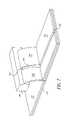
- FIGS. 1 and 2respectively show a cross-section view of one embodiment of the medium of the present invention and an exploded cross-section view of the embodiment of FIG. 1 .
- FIG. 3shows a top right perspective view of a base layer having an antenna layer formed thereon.
- base layer 20has a top surface 22 and a bottom surface 24 .
- Base layer 20can be formed from a material such as a paper, plastic, metal or other convenient substrate.
- the material used in base layer 20is selected to receive image forming materials such as inks, dyes, toners, and colorants. This permits images to be formed for example on bottom surface 24 using ink jet printing, thermal printing, contact press printing and other techniques.
- base layer 20can also be formed from a material that forms images when exposed to energy such thermal, electrical, optical, electromagnetic or other forms.
- top surface 22 or bottom surface 24 of base layer 20can be adapted by chemical or other treatments or coatings to receive images.
- base layer 20has a thickness of approximately 100 microns however, the thickness of base layer 20 is not critical.
- an optional antenna layer 30is formed on top surface 22 of base layer 20 .
- Antenna layer 30typically comprises a material that is capable of being used to form an antenna. Examples of such materials include metals such as copper, aluminum and other materials having electrically conductive properties.
- Antenna layer 30has patterned antennas 40 formed therein.
- FIG. 3shows a top view of a base layer 20 having patterned antennas 40 applied thereon.
- patterned antennas 40are arranged in a first row of antennas 32 and a second row of antennas 34 .
- Each one of patterned antennas 40has an antenna section 42 and mating surfaces 44 .
- rows of antennas 32 and 34extend longitudinally along top surface 22 of base layer 20 .
- such antennascan be arranged on antenna layer 30 in any useful pattern.
- each of patterned antennas 40is formed from patterns of antenna layer 30 and spaces 36 in antenna layer 30 .
- the arrangement of spaces 36 that form the pattern of material comprising patterned antennas 40can be formed by applying antenna layer 30 to top surface 22 in a patterned fashion. This can be done for example by using printing, lamination, thermal transfer, or laser thermal transfer techniques to selectively transfer antenna layer 30 to top surface 22 .
- antenna layer 30can be applied to top surface 22 to form a uniform layer, and portions of antenna layer 30 can be selectively removed to form spaces 36 . This selective removal can be done by etching or oblation processes that chemically, optically, thermally remove material from antenna layer 30 to form spaces 36 that define patterned antennas 40 .
- a material layer 50is applied to top surface 22 of base layer 20 and/or to antenna layer 30 .
- Material layer 50can comprise a material including paper, film, polymer or other materials.
- material layer 50is formed from BUTVAR polyvinyl butgral (PVB) resin sold commercially by Solutial, St. Louis, Mo., U.S.A.
- PVBBUTVAR polyvinyl butgral
- material layer 50is adapted to receive image forming substances such as inks, dyes, pigments, colorants, used in the formation of images.
- material layer 50can be formed from a material that forms images when exposed to energy such as thermal, electrical optical, electromagnetic or other form.
- Material layer 50can also be chemically treated to adapt material layer 50 to receive images or to facilitate modification of the material layer to permit formation of images thereon.
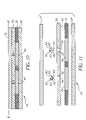
- voids 52are formed from material layer 50 .
- FIG. 4shows a top perspective view of medium 10 having an antenna layer 30 coated with a material layer 50 having voids 52 formed therein.
- voids 52expose antenna layer 40 so that transponder 60 can engage antenna mating surfaces 44 on antenna layer 40 to cooperate electrically therewith.
- Antenna engagement surfaces 62are provided on each of the transponders 60 to engage mating surfaces 44 .
- antenna engagement surfaces 62engage mating surfaces 44 to provide an electrical connection between transponders 60 and an antenna such as antenna 32 .
- transponder 60can receive electromagnetic signals and convert such signals into power to operates the transponders 60 .
- radio frequency communication circuit 63uses the electrical connection between mating surfaces 44 and antenna engagement surfaces 62 to transmit radio frequency signals that contain data from a memory 65 .
- Radio frequency communication circuit 63can also be adapted to use the electrical connection between engagement surfaces 62 and antenna mating surfaces 44 to receive radio frequency signals having data and to store the data from such signals in memory 63 .
- transponder 60will incorporate an antenna.
- voids 52are sized to receive transponders 60 having width dimensions 56 and 57 that are at least equal to a width dimension 64 of transponders 60 .
- the width dimensions 56 and 57 of voids 52respectively can be undersized with respect to the width dimension 64 of transponders 60 .
- voids 52are undersized, insertion of transponders 60 into voids 52 causes deformation of material layer 50 to allow transponders 60 to be inserted into voids 52 . Material layer 50 resists this deformation and applies a force against transponders 60 .
- This forcetends to hold transponders 60 within voids 52 and can be used to hold transponders 60 so that engagement surfaces 62 remain in contact with mating surfaces 44 of antennas 40 and do not slide along voids 52 in a manner that would cause separation of engagement surfaces 60 from mating surfaces 44 .
- material layer 50has a thickness 58 that is at least as thick as the thickness 67 of transponders 60 .
- an outer surface 55 of material layer 50 and outer surfaces 69 of transponders 60form a common plane A—A to provide a level surface that can be processed without risk of interference with later material handling.
- Thispermits the use of useful medium fabrication processes such as rolling or extrusion after transponders 60 have been joined to medium 10 and lowers the risk damage to previous and/or subsequently applied layers of medium 10 where medium 10 is wound onto rolls during further processing.
- the portions of voids 52 that are not occupied by transponders 60can be filled with material to provide a common plane in other portions of medium 10 and to help secure the position of transponders 60 in voids 52 .
- These unoccupied portions of voids 52can be filled with additional material of the type used to form material layer 50 .
- These portionscan also be filled with other convenient materials such as adhesives.
- material layer 50can have a thickness 58 that is at least greater than the thickness 67 of transponder 60 .
- a material layer 50 having void 52can be formed on a base layer 20 and/or on antenna layer 30 using various methods.
- FIGS. 5–9show examples of these methods.
- FIGS. 5 and 6show an example of a gap coating method.
- a supply 80 of material that forms material layer 50is applied to base layer 20 using a convenient means adapted for such material.
- Base layer 20 and the supply of material applied to base layer 20are passed between a roller 81 and limiting structure 84 such as a knife. As the material that forms material layer 50 and base layer 20 passes between roller 81 and limiting structure 84 , excess material is scraped off. This provides a uniform material layer 50 on base layer 20 .
- a stop 86is provided in limiting structure 84 .
- stop 86blocks material forming material layer 50 from passing and creates a void 52 in the material layer 50 .
- void 52 in material layer 50will have a slot shaped void extending longitudinally along material layer 50 . Stop 86 can also be selectively moved into and out of material layer 50 so as to create an intermittent void 52 .
- FIG. 7shows another embodiment of a method for forming a void 52 in a material layer 50 on a base layer 20 using a technique known as curtain coating.
- curtain coatinga material to be used to form material layer 50 flows from a supply 88 in a continuous curtain 90 onto base layer 20 as base layer 20 is passed through the flow.
- a stop 92interrupts the flow from supply 86 in create a space 94 in continuous curtain 90 which results in a void 52 in material layer 50 .
- FIGS. 8 and 9show still another embodiment of a method for forming a void in a material layer 50 .
- a technique known as slot die coatingis used.
- a supply 95has a slot 96 that ejects material onto base layer 20 to form a material layer 50 thereon as the base 20 is moved relative to slot by a roller 98 .
- a strip 99interrupts the flow of the material onto base layer 20 creating a void 52 in material layer 50 .
- other techniquescan also be used to form material layer 50 including but not limited to spraying and printing.
- an overcoat layer 70can be applied to material layer 50 .
- Overcoat layer 70secures transponders 60 in voids 52 . Further, overcoat layer 70 seals and fills material layer 50 so that no portion of antenna layer 40 remains exposed after overcoat layer 70 has been applied.
- Overcoat layer 70can be applied to fill portions of voids 52 that are not occupied by transponders 60 . This helps to secure transponder 60 and prevent movement of transponder 60 along voids 52 .
- Overcoat layer 70can be adapted to receive image-forming materials. In the embodiment that is shown in FIGS.
- overcoat layer 70is applied to form an outer surface 72 along plane B—B that does not have protrusions or other non-uniform areas caused by spaces 36 , antennas 40 , voids 52 and/or transponders 60 .
- Overcoat layer 70can also be adapted to cushion and protect transponders 60 , antennas 40 and medium 20 from chemical, thermal, radiation or mechanical damage during handling or manipulation of medium 20 .
- overcoat layer 70it is not essential that material layer 50 has a thickness that is at least as great as the thickness of transponders 60 . This is because a common plane e.g. B—B can be formed by an outer surface 72 of overcoat layer 70 wherein overcoat layer 70 is applied to a thickness that, in combination with material layer 50 has a thickness that is at least as thick as the thickness of transponders 60 .
- overcoat layer 70can comprise a transparent material that blocks the flow of ultraviolet or other forms of radiation, that provides protection against mechanical, thermal, chemical or other factors that may damage the appearance of the images formed on material layer 50 .
- an additional antenna layer 110can be formed on bottom surface 24 of base layer 20 . Additional antenna layer 110 can be formed in the manner described above with respect to forming antenna layer 40 . Similarly, an additional material layer 120 can be applied to additional antenna layer 110 with voids 112 formed therein. Voids 112 are adapted to receive transponders 60 and otherwise are similar to voids 52 as described above. As is also shown in FIG. 12 an additional overcoat layer 130 can optionally be applied to additional material layer 90 .
- Medium 10is free of protrusions, thus medium 10 can be further processed as necessary using conventional web forming techniques such as winding, rolling, extruding and printing can be applied to medium 10 after transponder 60 has been positioned in the material layer of medium 10 .
- a medium 10 having a transponders 60 attached theretocan be slit and wound onto rolls with each roll having at least one transponder 60 .
- Medium 10can also be slit and chopped into sheet form with each sheet having a transponder 60 associated therewith.
- an adhesive layer 140can be applied to base layer 20 of medium 10 to permit medium 10 to be easily applied to a tangible thing such as a bottle.
- An advantage of such a mediumis that a label can be provided that does not have a protrusion that might interfere with or be easily damaged by use and handling of the tangible thing to which the medium is attached.
- a removable layer 150can be applied to adhesive layer 140 .
- transponder 60can be formed in whole or in part by depositing circuit forming material on medium 20 .
- transponder 30can be formed on base layer 20 , antenna layer 30 , or in antenna layer 30 using lithographic, ink jet and other technologies that permit electronic circuits to be formed on a substrate.
- voids 52can incorporate void walls 54 that are shaped to align or otherwise position transponder 60 so that the antenna engagement surfaces 62 can engage mating surfaces 44 to provide an electrical connection between transponders 60 and an antenna such as antenna 32 .
- the shape of void walls 54can be matched to a particular footprint of a particular transponder 60 .
- FIGS. 14 and 15show cross sectional views of a void 52 having void walls 54 that are shaped with features to help receive and to hold transponder 60 in void 52 .
- void walls 54are narrower near outer surface 55 and wider near inner surface 53 .
- material layer 50is made from a material that permits some degree of elastic deformation. Accordingly, as shown in FIG. 11 when a transponder 60 is pressed into the portion of void walls 54 that is near outer surface 55 , material layer 50 deforms to accept transponder 60 into the portion of void walls 54 that is near inner surface 55 .
- the portion of void walls 54 near to the top surface of material layer 52then elastically expands as shown in FIG. 15 to capture transponder 30 in material layer 52 in an area proximate to antenna layer 30 .
Landscapes
- Engineering & Computer Science (AREA)
- Microelectronics & Electronic Packaging (AREA)
- Computer Hardware Design (AREA)
- Physics & Mathematics (AREA)
- General Physics & Mathematics (AREA)
- Theoretical Computer Science (AREA)
- Details Of Aerials (AREA)
- Credit Cards Or The Like (AREA)
Abstract
Description
- 10 medium
- 20 base layer
- 22 top surface of base layer
- 24 bottom surface of base layer
- 30 antenna layer
- 32 first row of antennas
- 34 second row of antennas
- 36 spaces in antenna layer
- 40 patterned antennas
- 42 antenna section
- 44 mating surfaces
- 50 material layer
- 52 voids
- 53 inner surface
- 55 outer surface
- 56 width dimension of void
- 57 width dimension of void
- 58 thickness of material layer
- 59 outer surface
- 60 transponder
- 61 power supply circuit
- 62 engagement surface
- 63 radio frequency communication circuit
- 64 width dimension of transponder
- 65 memory
- 66 Top surface of transponder
- 67 thickness of transponder
- 69 outer surface of material layer
- 70 overcoat layer
- 72 outer surface of overcoat layer
- 80 supply
- 81 roller
- 84 limiting structure
- 86 stop
- 88 supply
- 90 curtain
- 92 stop
- 94 space
- 95 supply
- 96 slot
- 98 roller
- 99 strip
- 110 additional antenna layer
- 112 voids
- 120 additional material layer
- 130 additional overcoat layer
- 140 adhesive layer
- 150 removable layer
Claims (12)
Priority Applications (3)
| Application Number | Priority Date | Filing Date | Title |
|---|---|---|---|
| US10/256,769US7233498B2 (en) | 2002-09-27 | 2002-09-27 | Medium having data storage and communication capabilities and method for forming same |
| EP03077890AEP1406209A3 (en) | 2002-09-27 | 2003-09-15 | Non-contact card with transponder placed in cavity of the card |
| JP2003332062AJP2004139583A (en) | 2002-09-27 | 2003-09-24 | Medium with data storing and communication capability, and production method |
Applications Claiming Priority (1)
| Application Number | Priority Date | Filing Date | Title |
|---|---|---|---|
| US10/256,769US7233498B2 (en) | 2002-09-27 | 2002-09-27 | Medium having data storage and communication capabilities and method for forming same |
Publications (2)
| Publication Number | Publication Date |
|---|---|
| US20040061994A1 US20040061994A1 (en) | 2004-04-01 |
| US7233498B2true US7233498B2 (en) | 2007-06-19 |
Family
ID=31993513
Family Applications (1)
| Application Number | Title | Priority Date | Filing Date |
|---|---|---|---|
| US10/256,769Expired - Fee RelatedUS7233498B2 (en) | 2002-09-27 | 2002-09-27 | Medium having data storage and communication capabilities and method for forming same |
Country Status (3)
| Country | Link |
|---|---|
| US (1) | US7233498B2 (en) |
| EP (1) | EP1406209A3 (en) |
| JP (1) | JP2004139583A (en) |
Cited By (2)
| Publication number | Priority date | Publication date | Assignee | Title |
|---|---|---|---|---|
| US20090115616A1 (en)* | 2007-11-06 | 2009-05-07 | Merrick Systems Inc. | RFID Transponder Enclosure for Harsh Environments |
| US20110017833A1 (en)* | 2004-02-12 | 2011-01-27 | Cullen James M | RFID tag and method of manufacturing the same |
Families Citing this family (19)
| Publication number | Priority date | Publication date | Assignee | Title |
|---|---|---|---|---|
| US6951596B2 (en)* | 2002-01-18 | 2005-10-04 | Avery Dennison Corporation | RFID label technique |
| US7002190B1 (en) | 2004-09-21 | 2006-02-21 | International Business Machines Corporation | Method of collector formation in BiCMOS technology |
| US7500307B2 (en)* | 2004-09-22 | 2009-03-10 | Avery Dennison Corporation | High-speed RFID circuit placement method |
| FR2882174B1 (en)* | 2005-02-11 | 2007-09-07 | Smart Packaging Solutions Sps | METHOD FOR MANUFACTURING A MICROELECTRONIC DEVICE WITH NON-CONTACT FUNCTIONING, IN PARTICULAR FOR ELECTRONIC PASSPORT |
| US7623034B2 (en)* | 2005-04-25 | 2009-11-24 | Avery Dennison Corporation | High-speed RFID circuit placement method and device |
| US7522056B2 (en) | 2005-05-24 | 2009-04-21 | V.H. Blackinton & Co., Inc. | Badge verification device |
| US20060292946A1 (en)* | 2005-06-22 | 2006-12-28 | Perfect Plastic Printing Corporation | Financial Transaction Card With Embedded Fabric |
| US7224278B2 (en) | 2005-10-18 | 2007-05-29 | Avery Dennison Corporation | Label with electronic components and method of making same |
| US7740179B2 (en)* | 2005-12-15 | 2010-06-22 | Mediamark Research, Inc. | System and method for RFID-based printed media reading activity data acquisition and analysis |
| US7959086B2 (en)* | 2005-12-15 | 2011-06-14 | Gfk Mediamark Research & Intelligence, Llc | System and method for RFID-based printed media reading activity data acquisition and analysis |
| US7555826B2 (en) | 2005-12-22 | 2009-07-07 | Avery Dennison Corporation | Method of manufacturing RFID devices |
| US8608080B2 (en)* | 2006-09-26 | 2013-12-17 | Feinics Amatech Teoranta | Inlays for security documents |
| WO2008037592A1 (en)* | 2006-09-26 | 2008-04-03 | Advanced Micromechanic And Automation Technology Ltd | Method of connecting an antenna to a transponder chip and corresponding transponder inlay |
| US7701352B2 (en)* | 2006-11-22 | 2010-04-20 | Avery Dennison Corporation | RFID label with release liner window, and method of making |
| US8094028B2 (en)* | 2007-12-28 | 2012-01-10 | Mckesson Automation, Inc. | Radio frequency alignment object, carriage and associated method of storing a product associated therewith |
| US8400277B2 (en)* | 2009-03-30 | 2013-03-19 | Mckesson Automation Inc. | Methods, apparatuses, and computer program products for monitoring a transfer of fluid between a syringe and a fluid reservoir |
| WO2011053182A1 (en)* | 2009-11-02 | 2011-05-05 | Leontiev Vladimir Vasilievich | Information storage and processing device (ispd) |
| US9171246B2 (en) | 2012-06-29 | 2015-10-27 | Aesynt Incorporated | System, methods, apparatuses, and computer program products for detecting that an object has been accessed |
| EP3432224B1 (en)* | 2016-03-18 | 2022-06-29 | Sato Holdings Kabushiki Kaisha | Method for manufacturing an rfid inlet |
Citations (109)
| Publication number | Priority date | Publication date | Assignee | Title |
|---|---|---|---|---|
| US3580565A (en) | 1968-12-11 | 1971-05-25 | Xerox Corp | Sheet feeding apparatus |
| US3713148A (en) | 1970-05-21 | 1973-01-23 | Communications Services Corp I | Transponder apparatus and system |
| US3835301A (en) | 1973-02-21 | 1974-09-10 | Helert P | Card coding and read-out system |
| US4075018A (en) | 1973-07-02 | 1978-02-21 | Peter Anderson Custer | Motion picture film, soundtrack and method for production thereof |
| US4129855A (en) | 1977-07-15 | 1978-12-12 | Rodrian J | Animal identification system |
| US4178183A (en) | 1978-07-27 | 1979-12-11 | Eastman Kodak Company | Thiazolyl coupler compositions and photographic elements suited to forming integral sound tracks |
| US4208210A (en) | 1974-12-19 | 1980-06-17 | Fuji Photo Film Co., Ltd. | Process for forming an optical soundtrack |
| US4247758A (en) | 1979-11-15 | 1981-01-27 | Rodrian James A | Animal identification and estrus detection system |
| US4270853A (en) | 1979-03-21 | 1981-06-02 | West Electric Company, Ltd. | Sound-recording instant-printing film and camera therefor |
| US4270854A (en) | 1978-09-14 | 1981-06-02 | Agfa-Gevaert, A.G. | Photographic instant camera with magnetic recording capability |
| US4600280A (en) | 1984-07-16 | 1986-07-15 | Clark Lloyd D | Digital audio recording/playback system for motion picture film |
| US4663625A (en) | 1983-11-30 | 1987-05-05 | Motion Magnetics Inc. | Passive tag identification system and method |
| US4742470A (en) | 1985-12-30 | 1988-05-03 | Gte Valeron Corporation | Tool identification system |
| US4806958A (en) | 1988-01-11 | 1989-02-21 | Eastman Kodak Company | Cassette/machine optically coupled interface |
| US4855769A (en) | 1988-08-29 | 1989-08-08 | Polaroid Corporation | Photographic apparatus for motorized processing of instant film |
| US4880325A (en) | 1980-03-17 | 1989-11-14 | Canon Kabushiki Kaisha | Ink ribbon cassette including means for identifying the type of ink ribbon contained therein and containing an ink ribbon having end indication means |
| US4905029A (en) | 1988-09-28 | 1990-02-27 | Kelley Scott A | Audio still camera system |
| US4983996A (en) | 1988-09-02 | 1991-01-08 | Casio Computer Co., Ltd. | Data recording apparatus for still camera |
| US4990092A (en) | 1989-08-14 | 1991-02-05 | Tonka Corporation | Talking book |
| US5008661A (en) | 1985-09-27 | 1991-04-16 | Raj Phani K | Electronic remote chemical identification system |
| US5019815A (en) | 1979-10-12 | 1991-05-28 | Lemelson Jerome H | Radio frequency controlled interrogator-responder system with passive code generator |
| US5030544A (en) | 1984-09-28 | 1991-07-09 | Agfa-Gevaert, N.V. | Photographic elements comprising thiazolyl couplers capable of forming infrared-absorbing dyes for integral sound track |
| US5049898A (en) | 1989-03-20 | 1991-09-17 | Hewlett-Packard Company | Printhead having memory element |
| US5049904A (en) | 1989-01-27 | 1991-09-17 | Shimadzu Corporation | Printer having identifiable interchangeable heads |
| US5059126A (en) | 1990-05-09 | 1991-10-22 | Kimball Dan V | Sound association and learning system |
| US5078523A (en) | 1988-03-04 | 1992-01-07 | Varitronic Systems, Inc. | Tape cassette with identifying circuit element for printing machine |
| US5105190A (en) | 1986-04-22 | 1992-04-14 | N.V. Nederlandsche Apparatenfabriek Nedap | Electromagnetic identification system |
| US5104247A (en) | 1989-07-18 | 1992-04-14 | Canon Kabushiki Kaisha | Recording control method, recording method, and recording apparatus for multicolor ink ribbon |
| US5184152A (en) | 1990-12-04 | 1993-02-02 | Sumimoto Electric Interconnect Products, Inc. | Printing apparatus and method for printing on an elongated member such as a tube |
| US5185315A (en) | 1991-02-21 | 1993-02-09 | Eastman Kodak Company | Making encoded dye-donor films for thermal printers |
| US5196862A (en) | 1992-02-21 | 1993-03-23 | Eastman Kodak Company | Apparatus and method for donor sensing at the print line in a thermal printer |
| US5196846A (en) | 1980-02-13 | 1993-03-23 | Brockelsby William K | Moving vehicle identification system |
| US5208450A (en)* | 1988-04-20 | 1993-05-04 | Matsushita Electric Industrial Co., Ltd. | IC card and a method for the manufacture of the same |
| US5224784A (en) | 1988-06-10 | 1993-07-06 | Ta Triumph-Adler | Electronically controlled typewriter, printer, or the like and ribbon cassette or type-wheel cassette therefor |
| US5266968A (en) | 1992-03-27 | 1993-11-30 | Eastman Kodak Company | Non-volatile memory thermal printer cartridge |
| US5266975A (en) | 1990-10-12 | 1993-11-30 | Seiko Epson Corporation | Ink jet printing apparatus having means for preventing excessive ink purging |
| US5268708A (en) | 1991-08-23 | 1993-12-07 | Eastman Kodak Company | Laser thermal printer with an automatic material supply |
| US5290190A (en) | 1992-09-30 | 1994-03-01 | Mcclanahan Susan D | Talking book |
| US5297881A (en) | 1991-05-16 | 1994-03-29 | Mitsubishi Steel Mfg. Co., Ltd. | Printing machine carriage having a magnetic encoder |
| US5305020A (en) | 1992-12-21 | 1994-04-19 | Tektronix, Inc. | Thermal transfer printer having media pre-coat selection apparatus and methods |
| US5310999A (en) | 1992-07-02 | 1994-05-10 | At&T Bell Laboratories | Secure toll collection system for moving vehicles |
| US5313235A (en) | 1989-05-12 | 1994-05-17 | Minolta Camera Kabushiki Kaisha | Sound playback apparatus capable of playing back sounds relevant to photographs |
| US5318370A (en) | 1992-11-17 | 1994-06-07 | Varitronic Systems, Inc. | Cartridge with data memory system and method regarding same |
| US5323704A (en) | 1992-07-30 | 1994-06-28 | Heidelberg-Harris Gmbh | Device for the identification of a flexible roller shell |
| US5331338A (en) | 1992-01-30 | 1994-07-19 | Printware, Inc. | Web steering for an image recorder |
| US5342671A (en) | 1992-06-05 | 1994-08-30 | Eastman Kodak Company | Encoded dye receiver |
| US5347274A (en) | 1990-05-17 | 1994-09-13 | At/Comm Incorporated | Hazardous waste transport management system |
| JPH0644265Y2 (en) | 1984-04-28 | 1994-11-14 | 昭和電線電纜株式会社 | Cable detention end |
| US5365312A (en) | 1988-07-25 | 1994-11-15 | Mannesmann Ag | Arrangement for printer equipment for monitoring reservoirs that contain printing medium |
| US5385416A (en) | 1991-12-13 | 1995-01-31 | Sony Corporation | Device for identifying an ink ribbon cartridge used in a printer |
| US5398257A (en) | 1993-01-11 | 1995-03-14 | Groenteman; Frank S. | Copier and monitoring network |
| US5412192A (en)* | 1993-07-20 | 1995-05-02 | American Express Company | Radio frequency activated charge card |
| US5430441A (en) | 1993-10-12 | 1995-07-04 | Motorola, Inc. | Transponding tag and method |
| US5455617A (en) | 1992-03-27 | 1995-10-03 | Eastman Kodak Company | Thermal printer supply having non-volatile memory |
| US5491327A (en) | 1994-08-10 | 1996-02-13 | American Magnetics Corporation | Universal magnetic medium encoder with tilt-compensating apparatus |
| US5491468A (en) | 1993-06-24 | 1996-02-13 | Westinghouse Electric Corporation | Identification system and method with passive tag |
| US5493385A (en) | 1994-12-09 | 1996-02-20 | Eastman Kodak Company | Electrophotographic color printer apparatus and method with improved registration of colors |
| US5504507A (en) | 1992-10-08 | 1996-04-02 | Xerox Corporation | Electronically readable performance data on a thermal ink jet printhead chip |
| US5513920A (en) | 1992-10-29 | 1996-05-07 | Eastman Kodak Company | Dye donor web loading apparatus for a thermal printer |
| US5516590A (en) | 1993-07-15 | 1996-05-14 | Ncr Corporation | Fluorescent security thermal transfer printing ribbons |
| US5521663A (en) | 1992-10-28 | 1996-05-28 | Norris, Iii; Wyamn J. | Sound system for still film photography |
| US5528377A (en) | 1994-03-29 | 1996-06-18 | E. I. Du Pont De Nemours And Company | Extended density color printing |
| US5528222A (en) | 1994-09-09 | 1996-06-18 | International Business Machines Corporation | Radio frequency circuit and memory in thin flexible package |
| US5530702A (en) | 1994-05-31 | 1996-06-25 | Ludwig Kipp | System for storage and communication of information |
| US5532727A (en) | 1993-01-28 | 1996-07-02 | Fuji Photo Film Co., Ltd. | Apparatus and method of thermally recording information with shading correction |
| US5537920A (en) | 1993-03-01 | 1996-07-23 | Riso Kagaku Corporation | Rotary stencil printing drum equipped with a wireless data communication device |
| US5547501A (en) | 1994-05-06 | 1996-08-20 | Kansai Paint Co., Ltd. | Method for formation of invisible marking and method for reading of invisible marking |
| US5559578A (en) | 1988-03-22 | 1996-09-24 | Hitachi, Ltd. | Electrostatic recording apparatus with electrified cap and managing system thereof |
| US5565906A (en) | 1994-01-13 | 1996-10-15 | Schoonscan, Inc. | Clocking means for bandwise imaging device |
| US5574519A (en) | 1994-05-03 | 1996-11-12 | Eastman Kodak Company | Talking photoalbum |
| US5584070A (en) | 1994-12-29 | 1996-12-10 | Motorola, Inc. | Wireless pager with separable receiver unit and transmitter unit |
| US5598201A (en) | 1994-01-31 | 1997-01-28 | Hewlett-Packard Company | Dual-resolution encoding system for high cyclic accuracy of print-medium advance in an inkjet printer |
| US5600350A (en) | 1993-04-30 | 1997-02-04 | Hewlett-Packard Company | Multiple inkjet print cartridge alignment by scanning a reference pattern and sampling same with reference to a position encoder |
| US5600352A (en) | 1994-06-27 | 1997-02-04 | Tektronix, Inc. | Apparatus and method for controlling coalescence of ink drops on a print medium |
| US5606347A (en) | 1992-12-16 | 1997-02-25 | Texas Instruments Incorporated | Devices systems and methods for flexible format data storage |
| US5610635A (en) | 1994-08-09 | 1997-03-11 | Encad, Inc. | Printer ink cartridge with memory storage capacity |
| US5620265A (en) | 1993-12-28 | 1997-04-15 | Sony Corporation | Ink ribbon cartridge |
| US5625391A (en) | 1991-12-13 | 1997-04-29 | Canon Kabushiki Kaisha | Ink jet recording method and apparatus |
| US5644557A (en) | 1993-12-22 | 1997-07-01 | Olympus Optical Co., Ltd. | Audio data recording system for recording voice data as an optically readable code on a recording medium for recording still image data photographed by a camera |
| US5647679A (en) | 1996-04-01 | 1997-07-15 | Itw Limited | Printer for printing on a continuous print medium |
| US5661515A (en) | 1993-01-22 | 1997-08-26 | Gerber Scientific Products, Inc. | Printer with feed fault detection |
| US5713288A (en) | 1995-08-03 | 1998-02-03 | Frazzitta; Joseph R. | Method and apparatus for use in offset printing |
| US5721992A (en) | 1995-03-28 | 1998-02-24 | Chovanes; Joseph E. | Method and apparatus for taking still pictures |
| WO1998009252A1 (en) | 1996-08-26 | 1998-03-05 | Tomas Meinen | Process for manufacturing chip cards |
| US5757021A (en) | 1995-02-17 | 1998-05-26 | Agfa-Gevaert N.V. | Identification system and method for use in the field of digital radiography |
| US5755519A (en) | 1996-12-04 | 1998-05-26 | Fargo Electronics, Inc. | Printer ribbon identification sensor |
| US5757394A (en) | 1995-09-27 | 1998-05-26 | Lexmark International, Inc. | Ink jet print head identification circuit with programmed transistor array |
| US5768633A (en) | 1996-09-03 | 1998-06-16 | Eastman Kodak Company | Tradeshow photographic and data transmission system |
| US5774752A (en) | 1996-12-26 | 1998-06-30 | Eastman Kodak Company | Processing of sound media with still image films in photofinishing labs |
| US5774639A (en) | 1995-02-17 | 1998-06-30 | Eastman Kodak Company | Printer media including compressed sensitometry curve information |
| US5812156A (en) | 1997-01-21 | 1998-09-22 | Hewlett-Packard Company | Apparatus controlled by data from consumable parts with incorporated memory devices |
| US5842118A (en) | 1996-12-18 | 1998-11-24 | Micron Communications, Inc. | Communication system including diversity antenna queuing |
| WO1998052762A3 (en) | 1997-05-20 | 1999-03-11 | Encad Inc | Intelligent printer components and printing system |
| US5913088A (en) | 1996-09-06 | 1999-06-15 | Eastman Kodak Company | Photographic system capable of creating and utilizing applets on photographic film |
| US5914671A (en) | 1997-02-27 | 1999-06-22 | Micron Communications, Inc. | System and method for locating individuals and equipment, airline reservation system, communication system |
| US6036099A (en)* | 1995-10-17 | 2000-03-14 | Leighton; Keith | Hot lamination process for the manufacture of a combination contact/contactless smart card and product resulting therefrom |
| US6075950A (en) | 1998-09-22 | 2000-06-13 | Eastman Kodak Company | Associating a sound record with a film image |
| US6100804A (en)* | 1998-10-29 | 2000-08-08 | Intecmec Ip Corp. | Radio frequency identification system |
| US6099178A (en) | 1998-08-12 | 2000-08-08 | Eastman Kodak Company | Printer with media supply spool adapted to sense type of media, and method of assembling same |
| US6106166A (en) | 1999-04-16 | 2000-08-22 | Eastman Kodak Company | Photoprocessing apparatus for sensing type of photoprocessing consumable and method of assembling the apparatus |
| DE20014076U1 (en) | 2000-08-11 | 2000-10-19 | Reiner Kartengeräte GmbH & Co. KG, 78120 Furtwangen | Chip card with adapter |
| US6173119B1 (en) | 1999-08-11 | 2001-01-09 | Eastman Kodak Company | Camera having radio-frequency identification transponder |
| US6263310B1 (en) | 1991-06-06 | 2001-07-17 | Lj Laboratories, L.L.C. | Method for producing remotely a commemorative device having an audio message circuit |
| US20010014377A1 (en) | 1999-01-13 | 2001-08-16 | Babb Susan M. | Label having a protective cavity and method of manufacture |
| US6282819B1 (en) | 1996-06-10 | 2001-09-04 | Jing Lu Gu | Design and manufacture of communicating card |
| US6404643B1 (en)* | 1998-10-15 | 2002-06-11 | Amerasia International Technology, Inc. | Article having an embedded electronic device, and method of making same |
| US20020101619A1 (en) | 2001-01-31 | 2002-08-01 | Hisayoshi Tsubaki | Image recording method and system, image transmitting method, and image recording apparatus |
| FR2775533B1 (en) | 1998-02-27 | 2003-02-14 | Gemplus Sca | ELECTRONIC DEVICE WITH NON-CONTACT ELECTRONIC MEMORY, AND METHOD FOR MANUFACTURING SUCH A DEVICE |
| US6595426B1 (en)* | 1997-10-03 | 2003-07-22 | Gemplus | Method of manufacturing an electronic device having a chip and/or an antenna, and a device obtained by implementing the method |
- 2002
- 2002-09-27USUS10/256,769patent/US7233498B2/ennot_activeExpired - Fee Related
- 2003
- 2003-09-15EPEP03077890Apatent/EP1406209A3/ennot_activeWithdrawn
- 2003-09-24JPJP2003332062Apatent/JP2004139583A/enactivePending
Patent Citations (113)
| Publication number | Priority date | Publication date | Assignee | Title |
|---|---|---|---|---|
| US3580565A (en) | 1968-12-11 | 1971-05-25 | Xerox Corp | Sheet feeding apparatus |
| US3713148A (en) | 1970-05-21 | 1973-01-23 | Communications Services Corp I | Transponder apparatus and system |
| US3835301A (en) | 1973-02-21 | 1974-09-10 | Helert P | Card coding and read-out system |
| US4075018A (en) | 1973-07-02 | 1978-02-21 | Peter Anderson Custer | Motion picture film, soundtrack and method for production thereof |
| US4208210A (en) | 1974-12-19 | 1980-06-17 | Fuji Photo Film Co., Ltd. | Process for forming an optical soundtrack |
| US4129855A (en) | 1977-07-15 | 1978-12-12 | Rodrian J | Animal identification system |
| US4178183A (en) | 1978-07-27 | 1979-12-11 | Eastman Kodak Company | Thiazolyl coupler compositions and photographic elements suited to forming integral sound tracks |
| US4270854A (en) | 1978-09-14 | 1981-06-02 | Agfa-Gevaert, A.G. | Photographic instant camera with magnetic recording capability |
| US4270853A (en) | 1979-03-21 | 1981-06-02 | West Electric Company, Ltd. | Sound-recording instant-printing film and camera therefor |
| US5019815A (en) | 1979-10-12 | 1991-05-28 | Lemelson Jerome H | Radio frequency controlled interrogator-responder system with passive code generator |
| US4247758A (en) | 1979-11-15 | 1981-01-27 | Rodrian James A | Animal identification and estrus detection system |
| US5196846A (en) | 1980-02-13 | 1993-03-23 | Brockelsby William K | Moving vehicle identification system |
| US4880325A (en) | 1980-03-17 | 1989-11-14 | Canon Kabushiki Kaisha | Ink ribbon cassette including means for identifying the type of ink ribbon contained therein and containing an ink ribbon having end indication means |
| US4663625A (en) | 1983-11-30 | 1987-05-05 | Motion Magnetics Inc. | Passive tag identification system and method |
| JPH0644265Y2 (en) | 1984-04-28 | 1994-11-14 | 昭和電線電纜株式会社 | Cable detention end |
| US4600280A (en) | 1984-07-16 | 1986-07-15 | Clark Lloyd D | Digital audio recording/playback system for motion picture film |
| US5030544A (en) | 1984-09-28 | 1991-07-09 | Agfa-Gevaert, N.V. | Photographic elements comprising thiazolyl couplers capable of forming infrared-absorbing dyes for integral sound track |
| US5008661A (en) | 1985-09-27 | 1991-04-16 | Raj Phani K | Electronic remote chemical identification system |
| US4742470A (en) | 1985-12-30 | 1988-05-03 | Gte Valeron Corporation | Tool identification system |
| US5105190A (en) | 1986-04-22 | 1992-04-14 | N.V. Nederlandsche Apparatenfabriek Nedap | Electromagnetic identification system |
| US4806958A (en) | 1988-01-11 | 1989-02-21 | Eastman Kodak Company | Cassette/machine optically coupled interface |
| US5078523A (en) | 1988-03-04 | 1992-01-07 | Varitronic Systems, Inc. | Tape cassette with identifying circuit element for printing machine |
| US5559578A (en) | 1988-03-22 | 1996-09-24 | Hitachi, Ltd. | Electrostatic recording apparatus with electrified cap and managing system thereof |
| US5208450A (en)* | 1988-04-20 | 1993-05-04 | Matsushita Electric Industrial Co., Ltd. | IC card and a method for the manufacture of the same |
| US5224784A (en) | 1988-06-10 | 1993-07-06 | Ta Triumph-Adler | Electronically controlled typewriter, printer, or the like and ribbon cassette or type-wheel cassette therefor |
| US5365312A (en) | 1988-07-25 | 1994-11-15 | Mannesmann Ag | Arrangement for printer equipment for monitoring reservoirs that contain printing medium |
| US4855769A (en) | 1988-08-29 | 1989-08-08 | Polaroid Corporation | Photographic apparatus for motorized processing of instant film |
| US4983996A (en) | 1988-09-02 | 1991-01-08 | Casio Computer Co., Ltd. | Data recording apparatus for still camera |
| US4905029A (en) | 1988-09-28 | 1990-02-27 | Kelley Scott A | Audio still camera system |
| US5049904A (en) | 1989-01-27 | 1991-09-17 | Shimadzu Corporation | Printer having identifiable interchangeable heads |
| US5049898A (en) | 1989-03-20 | 1991-09-17 | Hewlett-Packard Company | Printhead having memory element |
| US5313235A (en) | 1989-05-12 | 1994-05-17 | Minolta Camera Kabushiki Kaisha | Sound playback apparatus capable of playing back sounds relevant to photographs |
| US5104247A (en) | 1989-07-18 | 1992-04-14 | Canon Kabushiki Kaisha | Recording control method, recording method, and recording apparatus for multicolor ink ribbon |
| US4990092A (en) | 1989-08-14 | 1991-02-05 | Tonka Corporation | Talking book |
| US4990092B1 (en) | 1989-08-14 | 1998-08-04 | Tonka Corp | Talking book |
| US5059126A (en) | 1990-05-09 | 1991-10-22 | Kimball Dan V | Sound association and learning system |
| US5347274A (en) | 1990-05-17 | 1994-09-13 | At/Comm Incorporated | Hazardous waste transport management system |
| US5266975A (en) | 1990-10-12 | 1993-11-30 | Seiko Epson Corporation | Ink jet printing apparatus having means for preventing excessive ink purging |
| US5184152A (en) | 1990-12-04 | 1993-02-02 | Sumimoto Electric Interconnect Products, Inc. | Printing apparatus and method for printing on an elongated member such as a tube |
| US5185315A (en) | 1991-02-21 | 1993-02-09 | Eastman Kodak Company | Making encoded dye-donor films for thermal printers |
| US5297881A (en) | 1991-05-16 | 1994-03-29 | Mitsubishi Steel Mfg. Co., Ltd. | Printing machine carriage having a magnetic encoder |
| US6263310B1 (en) | 1991-06-06 | 2001-07-17 | Lj Laboratories, L.L.C. | Method for producing remotely a commemorative device having an audio message circuit |
| US5268708A (en) | 1991-08-23 | 1993-12-07 | Eastman Kodak Company | Laser thermal printer with an automatic material supply |
| US5625391A (en) | 1991-12-13 | 1997-04-29 | Canon Kabushiki Kaisha | Ink jet recording method and apparatus |
| US5385416A (en) | 1991-12-13 | 1995-01-31 | Sony Corporation | Device for identifying an ink ribbon cartridge used in a printer |
| US5331338A (en) | 1992-01-30 | 1994-07-19 | Printware, Inc. | Web steering for an image recorder |
| US5196862A (en) | 1992-02-21 | 1993-03-23 | Eastman Kodak Company | Apparatus and method for donor sensing at the print line in a thermal printer |
| US5266968A (en) | 1992-03-27 | 1993-11-30 | Eastman Kodak Company | Non-volatile memory thermal printer cartridge |
| US5455617A (en) | 1992-03-27 | 1995-10-03 | Eastman Kodak Company | Thermal printer supply having non-volatile memory |
| US5342671A (en) | 1992-06-05 | 1994-08-30 | Eastman Kodak Company | Encoded dye receiver |
| US5426011A (en) | 1992-06-05 | 1995-06-20 | Eastman Kodak Company | Thermal printing process with an encoded dye receiver having a transparent magnetic layer |
| US5310999A (en) | 1992-07-02 | 1994-05-10 | At&T Bell Laboratories | Secure toll collection system for moving vehicles |
| US5323704A (en) | 1992-07-30 | 1994-06-28 | Heidelberg-Harris Gmbh | Device for the identification of a flexible roller shell |
| US5290190A (en) | 1992-09-30 | 1994-03-01 | Mcclanahan Susan D | Talking book |
| US5504507A (en) | 1992-10-08 | 1996-04-02 | Xerox Corporation | Electronically readable performance data on a thermal ink jet printhead chip |
| US5521663A (en) | 1992-10-28 | 1996-05-28 | Norris, Iii; Wyamn J. | Sound system for still film photography |
| US5513920A (en) | 1992-10-29 | 1996-05-07 | Eastman Kodak Company | Dye donor web loading apparatus for a thermal printer |
| US5562352A (en) | 1992-10-29 | 1996-10-08 | Eastman Kodak Company | Dye donor web loading apparatus for a thermal printer |
| US5318370A (en) | 1992-11-17 | 1994-06-07 | Varitronic Systems, Inc. | Cartridge with data memory system and method regarding same |
| US5606347A (en) | 1992-12-16 | 1997-02-25 | Texas Instruments Incorporated | Devices systems and methods for flexible format data storage |
| US5305020A (en) | 1992-12-21 | 1994-04-19 | Tektronix, Inc. | Thermal transfer printer having media pre-coat selection apparatus and methods |
| US5398257A (en) | 1993-01-11 | 1995-03-14 | Groenteman; Frank S. | Copier and monitoring network |
| US5661515A (en) | 1993-01-22 | 1997-08-26 | Gerber Scientific Products, Inc. | Printer with feed fault detection |
| US5532727A (en) | 1993-01-28 | 1996-07-02 | Fuji Photo Film Co., Ltd. | Apparatus and method of thermally recording information with shading correction |
| US5537920A (en) | 1993-03-01 | 1996-07-23 | Riso Kagaku Corporation | Rotary stencil printing drum equipped with a wireless data communication device |
| US5600350A (en) | 1993-04-30 | 1997-02-04 | Hewlett-Packard Company | Multiple inkjet print cartridge alignment by scanning a reference pattern and sampling same with reference to a position encoder |
| US5491468A (en) | 1993-06-24 | 1996-02-13 | Westinghouse Electric Corporation | Identification system and method with passive tag |
| US5516590A (en) | 1993-07-15 | 1996-05-14 | Ncr Corporation | Fluorescent security thermal transfer printing ribbons |
| US5412192A (en)* | 1993-07-20 | 1995-05-02 | American Express Company | Radio frequency activated charge card |
| US5430441A (en) | 1993-10-12 | 1995-07-04 | Motorola, Inc. | Transponding tag and method |
| US5644557A (en) | 1993-12-22 | 1997-07-01 | Olympus Optical Co., Ltd. | Audio data recording system for recording voice data as an optically readable code on a recording medium for recording still image data photographed by a camera |
| US5620265A (en) | 1993-12-28 | 1997-04-15 | Sony Corporation | Ink ribbon cartridge |
| US5565906A (en) | 1994-01-13 | 1996-10-15 | Schoonscan, Inc. | Clocking means for bandwise imaging device |
| US5598201A (en) | 1994-01-31 | 1997-01-28 | Hewlett-Packard Company | Dual-resolution encoding system for high cyclic accuracy of print-medium advance in an inkjet printer |
| US5528377A (en) | 1994-03-29 | 1996-06-18 | E. I. Du Pont De Nemours And Company | Extended density color printing |
| US5574519A (en) | 1994-05-03 | 1996-11-12 | Eastman Kodak Company | Talking photoalbum |
| US5547501A (en) | 1994-05-06 | 1996-08-20 | Kansai Paint Co., Ltd. | Method for formation of invisible marking and method for reading of invisible marking |
| US5530702A (en) | 1994-05-31 | 1996-06-25 | Ludwig Kipp | System for storage and communication of information |
| US5600352A (en) | 1994-06-27 | 1997-02-04 | Tektronix, Inc. | Apparatus and method for controlling coalescence of ink drops on a print medium |
| US5610635A (en) | 1994-08-09 | 1997-03-11 | Encad, Inc. | Printer ink cartridge with memory storage capacity |
| US5491327A (en) | 1994-08-10 | 1996-02-13 | American Magnetics Corporation | Universal magnetic medium encoder with tilt-compensating apparatus |
| US5528222A (en) | 1994-09-09 | 1996-06-18 | International Business Machines Corporation | Radio frequency circuit and memory in thin flexible package |
| US5493385A (en) | 1994-12-09 | 1996-02-20 | Eastman Kodak Company | Electrophotographic color printer apparatus and method with improved registration of colors |
| US5584070A (en) | 1994-12-29 | 1996-12-10 | Motorola, Inc. | Wireless pager with separable receiver unit and transmitter unit |
| US5757021A (en) | 1995-02-17 | 1998-05-26 | Agfa-Gevaert N.V. | Identification system and method for use in the field of digital radiography |
| US5774639A (en) | 1995-02-17 | 1998-06-30 | Eastman Kodak Company | Printer media including compressed sensitometry curve information |
| US5721992A (en) | 1995-03-28 | 1998-02-24 | Chovanes; Joseph E. | Method and apparatus for taking still pictures |
| US5713288A (en) | 1995-08-03 | 1998-02-03 | Frazzitta; Joseph R. | Method and apparatus for use in offset printing |
| US5757394A (en) | 1995-09-27 | 1998-05-26 | Lexmark International, Inc. | Ink jet print head identification circuit with programmed transistor array |
| US6036099A (en)* | 1995-10-17 | 2000-03-14 | Leighton; Keith | Hot lamination process for the manufacture of a combination contact/contactless smart card and product resulting therefrom |
| US5647679A (en) | 1996-04-01 | 1997-07-15 | Itw Limited | Printer for printing on a continuous print medium |
| US6282819B1 (en) | 1996-06-10 | 2001-09-04 | Jing Lu Gu | Design and manufacture of communicating card |
| WO1998009252A1 (en) | 1996-08-26 | 1998-03-05 | Tomas Meinen | Process for manufacturing chip cards |
| US5768633A (en) | 1996-09-03 | 1998-06-16 | Eastman Kodak Company | Tradeshow photographic and data transmission system |
| US5913088A (en) | 1996-09-06 | 1999-06-15 | Eastman Kodak Company | Photographic system capable of creating and utilizing applets on photographic film |
| US5755519A (en) | 1996-12-04 | 1998-05-26 | Fargo Electronics, Inc. | Printer ribbon identification sensor |
| US5842118A (en) | 1996-12-18 | 1998-11-24 | Micron Communications, Inc. | Communication system including diversity antenna queuing |
| US5774752A (en) | 1996-12-26 | 1998-06-30 | Eastman Kodak Company | Processing of sound media with still image films in photofinishing labs |
| US5812156A (en) | 1997-01-21 | 1998-09-22 | Hewlett-Packard Company | Apparatus controlled by data from consumable parts with incorporated memory devices |
| US5914671A (en) | 1997-02-27 | 1999-06-22 | Micron Communications, Inc. | System and method for locating individuals and equipment, airline reservation system, communication system |
| WO1998052762A3 (en) | 1997-05-20 | 1999-03-11 | Encad Inc | Intelligent printer components and printing system |
| US6227643B1 (en) | 1997-05-20 | 2001-05-08 | Encad, Inc. | Intelligent printer components and printing system |
| US6595426B1 (en)* | 1997-10-03 | 2003-07-22 | Gemplus | Method of manufacturing an electronic device having a chip and/or an antenna, and a device obtained by implementing the method |
| FR2775533B1 (en) | 1998-02-27 | 2003-02-14 | Gemplus Sca | ELECTRONIC DEVICE WITH NON-CONTACT ELECTRONIC MEMORY, AND METHOD FOR MANUFACTURING SUCH A DEVICE |
| US6099178A (en) | 1998-08-12 | 2000-08-08 | Eastman Kodak Company | Printer with media supply spool adapted to sense type of media, and method of assembling same |
| US6075950A (en) | 1998-09-22 | 2000-06-13 | Eastman Kodak Company | Associating a sound record with a film image |
| US6404643B1 (en)* | 1998-10-15 | 2002-06-11 | Amerasia International Technology, Inc. | Article having an embedded electronic device, and method of making same |
| US6100804A (en)* | 1998-10-29 | 2000-08-08 | Intecmec Ip Corp. | Radio frequency identification system |
| US20010014377A1 (en) | 1999-01-13 | 2001-08-16 | Babb Susan M. | Label having a protective cavity and method of manufacture |
| US6106166A (en) | 1999-04-16 | 2000-08-22 | Eastman Kodak Company | Photoprocessing apparatus for sensing type of photoprocessing consumable and method of assembling the apparatus |
| US6173119B1 (en) | 1999-08-11 | 2001-01-09 | Eastman Kodak Company | Camera having radio-frequency identification transponder |
| DE20014076U1 (en) | 2000-08-11 | 2000-10-19 | Reiner Kartengeräte GmbH & Co. KG, 78120 Furtwangen | Chip card with adapter |
| US20020101619A1 (en) | 2001-01-31 | 2002-08-01 | Hisayoshi Tsubaki | Image recording method and system, image transmitting method, and image recording apparatus |
Non-Patent Citations (11)
| Title |
|---|
| Atmel Smart Card ICs, Atmel Corp., San Jose, CA. |
| Latest Generation Technology for Immobilizer Systems, by Knebelkamp et al. Published by Texas Instruments, Dallas, Texas www.ti.com.tiris.docs.manuals/whtPapers/immobilizer.pdf. |
| Making RFID work for you: An Industry Roundtable hosted by Texas Instruments at NACS-Tech 1998, Published by Texas Instruments, Dallas, Texas, 2000 www.ti.com/tiris/docs/manuals/whtPapers/manuf-dist.pdf. |
| Multi-Technology Card Guide, HID Corporation, An ASSA ABLOY Group Company. |
| Protective Security Management, HID Prox Cards, www.prosecman.com. |
| ProxCard(R) II, Proximity Acces Card, HID Corp. An ASSA ABLOY Group Company, (C) 2001. |
| ProxCard® II, Proximity Acces Card, HID Corp. An ASSA ABLOY Group Company, © 2001. |
| Tag-it-Moving Concepts to Rality, Published by Texas Instruments, Dallas, Texas, 2000. |
| TEMIC Semiconductors e5550, Standard Read/Write Identification IC, TELEFUNKEN Semiconductors, Rev. A3, Mar. 17, 1998. |
| TEMIC Semiconductors TK5550, Read/Write Transponder, Transponder, TELEFUNKEN Semiconductors, Rev. A1, Apr. 30, 1997. |
| TheCutting Edge of RFID Technology and Applications for Manufacturing and Distribution, by d'Hont, Published by Texas Instruments, Dallas, Texas, 2000 www.ti.com/tiris/docs/manuals/whtPapers/manuf-dist.pdf. |
Cited By (4)
| Publication number | Priority date | Publication date | Assignee | Title |
|---|---|---|---|---|
| US20110017833A1 (en)* | 2004-02-12 | 2011-01-27 | Cullen James M | RFID tag and method of manufacturing the same |
| US8212676B2 (en)* | 2004-02-12 | 2012-07-03 | Avery Dennison Corporation | RFID tag and method of manufacturing the same |
| US20090115616A1 (en)* | 2007-11-06 | 2009-05-07 | Merrick Systems Inc. | RFID Transponder Enclosure for Harsh Environments |
| US8120497B2 (en)* | 2007-11-06 | 2012-02-21 | Merrick Systems, Inc. | RFID transponder enclosure for harsh environments |
Also Published As
| Publication number | Publication date |
|---|---|
| JP2004139583A (en) | 2004-05-13 |
| US20040061994A1 (en) | 2004-04-01 |
| EP1406209A2 (en) | 2004-04-07 |
| EP1406209A3 (en) | 2006-05-31 |
Similar Documents
| Publication | Publication Date | Title |
|---|---|---|
| US7233498B2 (en) | Medium having data storage and communication capabilities and method for forming same | |
| US6851617B2 (en) | Laser imageable RFID label/tag | |
| US7845569B1 (en) | Permanent RFID luggage tag with security features | |
| EP1467315A2 (en) | Medium having data storage and communication capabilities and method for forming same | |
| US20040062016A1 (en) | Medium having data storage and communication capabilites and method for forming same | |
| JP4590908B2 (en) | Non-contact IC medium and method of manufacturing non-contact IC medium | |
| JP3953775B2 (en) | Multi-contact substrate for non-contact data carrier and multi-contact non-contact data carrier | |
| JP2005222277A (en) | Information recording medium | |
| JP3716087B2 (en) | IC card issuing system and IC card issuing method | |
| JP4048788B2 (en) | card | |
| JPH08123926A (en) | Information storage carrier and manufacturing method thereof | |
| JP4736583B2 (en) | Non-contact IC media | |
| JP4882187B2 (en) | Contactless IC card and contactless IC card sending medium | |
| JP4529486B2 (en) | Non-contact IC media | |
| JP4028223B2 (en) | card case | |
| JP2008052541A (en) | Method for manufacturing IC card having magnetic recording layer | |
| JP2003067716A (en) | Non-contact IC card, non-contact IC card sending medium, and manufacturing method thereof | |
| JP2003067706A (en) | Non-contact IC card recording medium and method of manufacturing the same | |
| JP2005284813A (en) | Manufacturing method of RF-ID media | |
| JP4580944B2 (en) | Non-contact data carrier and manufacturing method thereof | |
| JP2011150409A (en) | Security document | |
| JP2007011441A (en) | Ic card | |
| JP2003044819A (en) | Recording medium and method of manufacturing the same | |
| JP2007007901A (en) | Identification card | |
| WO2006054468A1 (en) | Id card manufacturing method and test card used therein |
Legal Events
| Date | Code | Title | Description |
|---|---|---|---|
| AS | Assignment | Owner name:EASTMAN KODAK COMPANY, NEW YORK Free format text:ASSIGNMENT OF ASSIGNORS INTEREST;ASSIGNORS:KERR, ROGER S.;TREDWELL, TIMOTHY J.;REEL/FRAME:013350/0940 Effective date:20020926 | |
| FEPP | Fee payment procedure | Free format text:PAYOR NUMBER ASSIGNED (ORIGINAL EVENT CODE: ASPN); ENTITY STATUS OF PATENT OWNER: LARGE ENTITY | |
| STCF | Information on status: patent grant | Free format text:PATENTED CASE | |
| FPAY | Fee payment | Year of fee payment:4 | |
| AS | Assignment | Owner name:CITICORP NORTH AMERICA, INC., AS AGENT, NEW YORK Free format text:SECURITY INTEREST;ASSIGNORS:EASTMAN KODAK COMPANY;PAKON, INC.;REEL/FRAME:028201/0420 Effective date:20120215 | |
| AS | Assignment | Owner name:WILMINGTON TRUST, NATIONAL ASSOCIATION, AS AGENT, MINNESOTA Free format text:PATENT SECURITY AGREEMENT;ASSIGNORS:EASTMAN KODAK COMPANY;PAKON, INC.;REEL/FRAME:030122/0235 Effective date:20130322 Owner name:WILMINGTON TRUST, NATIONAL ASSOCIATION, AS AGENT, Free format text:PATENT SECURITY AGREEMENT;ASSIGNORS:EASTMAN KODAK COMPANY;PAKON, INC.;REEL/FRAME:030122/0235 Effective date:20130322 | |
| AS | Assignment | Owner name:BANK OF AMERICA N.A., AS AGENT, MASSACHUSETTS Free format text:INTELLECTUAL PROPERTY SECURITY AGREEMENT (ABL);ASSIGNORS:EASTMAN KODAK COMPANY;FAR EAST DEVELOPMENT LTD.;FPC INC.;AND OTHERS;REEL/FRAME:031162/0117 Effective date:20130903 Owner name:JPMORGAN CHASE BANK, N.A., AS ADMINISTRATIVE, DELAWARE Free format text:INTELLECTUAL PROPERTY SECURITY AGREEMENT (FIRST LIEN);ASSIGNORS:EASTMAN KODAK COMPANY;FAR EAST DEVELOPMENT LTD.;FPC INC.;AND OTHERS;REEL/FRAME:031158/0001 Effective date:20130903 Owner name:BARCLAYS BANK PLC, AS ADMINISTRATIVE AGENT, NEW YORK Free format text:INTELLECTUAL PROPERTY SECURITY AGREEMENT (SECOND LIEN);ASSIGNORS:EASTMAN KODAK COMPANY;FAR EAST DEVELOPMENT LTD.;FPC INC.;AND OTHERS;REEL/FRAME:031159/0001 Effective date:20130903 Owner name:EASTMAN KODAK COMPANY, NEW YORK Free format text:RELEASE OF SECURITY INTEREST IN PATENTS;ASSIGNORS:CITICORP NORTH AMERICA, INC., AS SENIOR DIP AGENT;WILMINGTON TRUST, NATIONAL ASSOCIATION, AS JUNIOR DIP AGENT;REEL/FRAME:031157/0451 Effective date:20130903 Owner name:PAKON, INC., NEW YORK Free format text:RELEASE OF SECURITY INTEREST IN PATENTS;ASSIGNORS:CITICORP NORTH AMERICA, INC., AS SENIOR DIP AGENT;WILMINGTON TRUST, NATIONAL ASSOCIATION, AS JUNIOR DIP AGENT;REEL/FRAME:031157/0451 Effective date:20130903 Owner name:BARCLAYS BANK PLC, AS ADMINISTRATIVE AGENT, NEW YO Free format text:INTELLECTUAL PROPERTY SECURITY AGREEMENT (SECOND LIEN);ASSIGNORS:EASTMAN KODAK COMPANY;FAR EAST DEVELOPMENT LTD.;FPC INC.;AND OTHERS;REEL/FRAME:031159/0001 Effective date:20130903 Owner name:JPMORGAN CHASE BANK, N.A., AS ADMINISTRATIVE, DELA Free format text:INTELLECTUAL PROPERTY SECURITY AGREEMENT (FIRST LIEN);ASSIGNORS:EASTMAN KODAK COMPANY;FAR EAST DEVELOPMENT LTD.;FPC INC.;AND OTHERS;REEL/FRAME:031158/0001 Effective date:20130903 | |
| FPAY | Fee payment | Year of fee payment:8 | |
| FEPP | Fee payment procedure | Free format text:MAINTENANCE FEE REMINDER MAILED (ORIGINAL EVENT CODE: REM.); ENTITY STATUS OF PATENT OWNER: LARGE ENTITY | |
| AS | Assignment | Owner name:FPC, INC., NEW YORK Free format text:RELEASE BY SECURED PARTY;ASSIGNOR:JP MORGAN CHASE BANK, N.A., AS ADMINISTRATIVE AGENT;REEL/FRAME:049814/0001 Effective date:20190617 Owner name:NPEC, INC., NEW YORK Free format text:RELEASE BY SECURED PARTY;ASSIGNOR:JP MORGAN CHASE BANK, N.A., AS ADMINISTRATIVE AGENT;REEL/FRAME:049814/0001 Effective date:20190617 Owner name:QUALEX, INC., NEW YORK Free format text:RELEASE BY SECURED PARTY;ASSIGNOR:JP MORGAN CHASE BANK, N.A., AS ADMINISTRATIVE AGENT;REEL/FRAME:049814/0001 Effective date:20190617 Owner name:KODAK AVIATION LEASING LLC, NEW YORK Free format text:RELEASE BY SECURED PARTY;ASSIGNOR:JP MORGAN CHASE BANK, N.A., AS ADMINISTRATIVE AGENT;REEL/FRAME:049814/0001 Effective date:20190617 Owner name:KODAK PORTUGUESA LIMITED, NEW YORK Free format text:RELEASE BY SECURED PARTY;ASSIGNOR:JP MORGAN CHASE BANK, N.A., AS ADMINISTRATIVE AGENT;REEL/FRAME:049814/0001 Effective date:20190617 Owner name:FAR EAST DEVELOPMENT LTD., NEW YORK Free format text:RELEASE BY SECURED PARTY;ASSIGNOR:JP MORGAN CHASE BANK, N.A., AS ADMINISTRATIVE AGENT;REEL/FRAME:049814/0001 Effective date:20190617 Owner name:LASER PACIFIC MEDIA CORPORATION, NEW YORK Free format text:RELEASE BY SECURED PARTY;ASSIGNOR:JP MORGAN CHASE BANK, N.A., AS ADMINISTRATIVE AGENT;REEL/FRAME:049814/0001 Effective date:20190617 Owner name:CREO MANUFACTURING AMERICA LLC, NEW YORK Free format text:RELEASE BY SECURED PARTY;ASSIGNOR:JP MORGAN CHASE BANK, N.A., AS ADMINISTRATIVE AGENT;REEL/FRAME:049814/0001 Effective date:20190617 Owner name:KODAK REALTY, INC., NEW YORK Free format text:RELEASE BY SECURED PARTY;ASSIGNOR:JP MORGAN CHASE BANK, N.A., AS ADMINISTRATIVE AGENT;REEL/FRAME:049814/0001 Effective date:20190617 Owner name:KODAK IMAGING NETWORK, INC., NEW YORK Free format text:RELEASE BY SECURED PARTY;ASSIGNOR:JP MORGAN CHASE BANK, N.A., AS ADMINISTRATIVE AGENT;REEL/FRAME:049814/0001 Effective date:20190617 Owner name:EASTMAN KODAK COMPANY, NEW YORK Free format text:RELEASE BY SECURED PARTY;ASSIGNOR:JP MORGAN CHASE BANK, N.A., AS ADMINISTRATIVE AGENT;REEL/FRAME:049814/0001 Effective date:20190617 Owner name:PAKON, INC., NEW YORK Free format text:RELEASE BY SECURED PARTY;ASSIGNOR:JP MORGAN CHASE BANK, N.A., AS ADMINISTRATIVE AGENT;REEL/FRAME:049814/0001 Effective date:20190617 Owner name:KODAK AMERICAS, LTD., NEW YORK Free format text:RELEASE BY SECURED PARTY;ASSIGNOR:JP MORGAN CHASE BANK, N.A., AS ADMINISTRATIVE AGENT;REEL/FRAME:049814/0001 Effective date:20190617 Owner name:KODAK (NEAR EAST), INC., NEW YORK Free format text:RELEASE BY SECURED PARTY;ASSIGNOR:JP MORGAN CHASE BANK, N.A., AS ADMINISTRATIVE AGENT;REEL/FRAME:049814/0001 Effective date:20190617 Owner name:KODAK PHILIPPINES, LTD., NEW YORK Free format text:RELEASE BY SECURED PARTY;ASSIGNOR:JP MORGAN CHASE BANK, N.A., AS ADMINISTRATIVE AGENT;REEL/FRAME:049814/0001 Effective date:20190617 | |
| LAPS | Lapse for failure to pay maintenance fees | Free format text:PATENT EXPIRED FOR FAILURE TO PAY MAINTENANCE FEES (ORIGINAL EVENT CODE: EXP.); ENTITY STATUS OF PATENT OWNER: LARGE ENTITY | |
| STCH | Information on status: patent discontinuation | Free format text:PATENT EXPIRED DUE TO NONPAYMENT OF MAINTENANCE FEES UNDER 37 CFR 1.362 | |
| FP | Lapsed due to failure to pay maintenance fee | Effective date:20190619 | |
| AS | Assignment | Owner name:KODAK REALTY INC., NEW YORK Free format text:RELEASE BY SECURED PARTY;ASSIGNOR:BARCLAYS BANK PLC;REEL/FRAME:052773/0001 Effective date:20170202 Owner name:KODAK PHILIPPINES LTD., NEW YORK Free format text:RELEASE BY SECURED PARTY;ASSIGNOR:BARCLAYS BANK PLC;REEL/FRAME:052773/0001 Effective date:20170202 Owner name:LASER PACIFIC MEDIA CORPORATION, NEW YORK Free format text:RELEASE BY SECURED PARTY;ASSIGNOR:BARCLAYS BANK PLC;REEL/FRAME:052773/0001 Effective date:20170202 Owner name:FAR EAST DEVELOPMENT LTD., NEW YORK Free format text:RELEASE BY SECURED PARTY;ASSIGNOR:BARCLAYS BANK PLC;REEL/FRAME:052773/0001 Effective date:20170202 Owner name:NPEC INC., NEW YORK Free format text:RELEASE BY SECURED PARTY;ASSIGNOR:BARCLAYS BANK PLC;REEL/FRAME:052773/0001 Effective date:20170202 Owner name:FPC INC., NEW YORK Free format text:RELEASE BY SECURED PARTY;ASSIGNOR:BARCLAYS BANK PLC;REEL/FRAME:052773/0001 Effective date:20170202 Owner name:KODAK (NEAR EAST) INC., NEW YORK Free format text:RELEASE BY SECURED PARTY;ASSIGNOR:BARCLAYS BANK PLC;REEL/FRAME:052773/0001 Effective date:20170202 Owner name:KODAK AMERICAS LTD., NEW YORK Free format text:RELEASE BY SECURED PARTY;ASSIGNOR:BARCLAYS BANK PLC;REEL/FRAME:052773/0001 Effective date:20170202 Owner name:EASTMAN KODAK COMPANY, NEW YORK Free format text:RELEASE BY SECURED PARTY;ASSIGNOR:BARCLAYS BANK PLC;REEL/FRAME:052773/0001 Effective date:20170202 Owner name:QUALEX INC., NEW YORK Free format text:RELEASE BY SECURED PARTY;ASSIGNOR:BARCLAYS BANK PLC;REEL/FRAME:052773/0001 Effective date:20170202 |