US7233024B2 - Three-dimensional memory device incorporating segmented bit line memory array - Google Patents
Three-dimensional memory device incorporating segmented bit line memory arrayDownload PDFInfo
- Publication number
- US7233024B2 US7233024B2US10/403,752US40375203AUS7233024B2US 7233024 B2US7233024 B2US 7233024B2US 40375203 AUS40375203 AUS 40375203AUS 7233024 B2US7233024 B2US 7233024B2
- Authority
- US
- United States
- Prior art keywords
- bit line
- memory
- layer
- global
- integrated circuit
- Prior art date
- Legal status (The legal status is an assumption and is not a legal conclusion. Google has not performed a legal analysis and makes no representation as to the accuracy of the status listed.)
- Expired - Lifetime, expires
Links
- 230000015654memoryEffects0.000titleclaimsabstractdescription413
- 239000003990capacitorSubstances0.000claimsdescription7
- 239000002305electric materialSubstances0.000claimsdescription5
- 230000008878couplingEffects0.000claimsdescription4
- 238000010168coupling processMethods0.000claimsdescription4
- 238000005859coupling reactionMethods0.000claimsdescription4
- 238000003491arrayMethods0.000abstractdescription41
- 230000000694effectsEffects0.000abstractdescription5
- 210000004027cellAnatomy0.000description162
- 239000010410layerSubstances0.000description148
- 238000010586diagramMethods0.000description24
- 238000000034methodMethods0.000description21
- 238000005516engineering processMethods0.000description12
- 238000004519manufacturing processMethods0.000description10
- 239000004065semiconductorSubstances0.000description8
- 230000008569processEffects0.000description7
- 238000013461designMethods0.000description6
- 239000000463materialSubstances0.000description6
- 230000008520organizationEffects0.000description5
- 230000008901benefitEffects0.000description4
- 238000011161developmentMethods0.000description4
- 230000018109developmental processEffects0.000description4
- 230000002829reductive effectEffects0.000description4
- 230000003213activating effectEffects0.000description3
- 238000007667floatingMethods0.000description3
- 238000002955isolationMethods0.000description3
- 239000011159matrix materialSubstances0.000description3
- 229910052710siliconInorganic materials0.000description3
- 239000010703siliconSubstances0.000description3
- XUIMIQQOPSSXEZ-UHFFFAOYSA-NSiliconChemical compound[Si]XUIMIQQOPSSXEZ-UHFFFAOYSA-N0.000description2
- 230000001186cumulative effectEffects0.000description2
- 230000001066destructive effectEffects0.000description2
- 230000001627detrimental effectEffects0.000description2
- 239000003989dielectric materialSubstances0.000description2
- 230000003993interactionEffects0.000description2
- 150000004767nitridesChemical class0.000description2
- 239000011368organic materialSubstances0.000description2
- 239000000047productSubstances0.000description2
- 230000002441reversible effectEffects0.000description2
- 238000012360testing methodMethods0.000description2
- 230000003466anti-cipated effectEffects0.000description1
- 230000003542behavioural effectEffects0.000description1
- 230000008859changeEffects0.000description1
- 238000004891communicationMethods0.000description1
- 230000002860competitive effectEffects0.000description1
- 230000009977dual effectEffects0.000description1
- 230000005684electric fieldEffects0.000description1
- 230000005669field effectEffects0.000description1
- 230000014509gene expressionEffects0.000description1
- 239000002784hot electronSubstances0.000description1
- 230000001788irregularEffects0.000description1
- 238000002372labellingMethods0.000description1
- 230000000670limiting effectEffects0.000description1
- 238000012986modificationMethods0.000description1
- 230000004048modificationEffects0.000description1
- 210000004457myocytus nodalisAnatomy0.000description1
- 230000003287optical effectEffects0.000description1
- BPUBBGLMJRNUCC-UHFFFAOYSA-Noxygen(2-);tantalum(5+)Chemical class[O-2].[O-2].[O-2].[O-2].[O-2].[Ta+5].[Ta+5]BPUBBGLMJRNUCC-UHFFFAOYSA-N0.000description1
- 230000036961partial effectEffects0.000description1
- 239000012782phase change materialSubstances0.000description1
- 230000010287polarizationEffects0.000description1
- 238000012545processingMethods0.000description1
- LIVNPJMFVYWSIS-UHFFFAOYSA-Nsilicon monoxideChemical class[Si-]#[O+]LIVNPJMFVYWSIS-UHFFFAOYSA-N0.000description1
- 229910052814silicon oxideInorganic materials0.000description1
- 238000004088simulationMethods0.000description1
- 239000002356single layerSubstances0.000description1
- 239000007787solidSubstances0.000description1
- 238000000638solvent extractionMethods0.000description1
- 239000000758substrateSubstances0.000description1
- 239000013589supplementSubstances0.000description1
- 229910001936tantalum oxideInorganic materials0.000description1
- 230000000007visual effectEffects0.000description1
Images


Classifications
- G—PHYSICS
- G11—INFORMATION STORAGE
- G11C—STATIC STORES
- G11C7/00—Arrangements for writing information into, or reading information out from, a digital store
- G11C7/18—Bit line organisation; Bit line lay-out
- G—PHYSICS
- G11—INFORMATION STORAGE
- G11C—STATIC STORES
- G11C16/00—Erasable programmable read-only memories
- G11C16/02—Erasable programmable read-only memories electrically programmable
- G11C16/04—Erasable programmable read-only memories electrically programmable using variable threshold transistors, e.g. FAMOS
- G11C16/0408—Erasable programmable read-only memories electrically programmable using variable threshold transistors, e.g. FAMOS comprising cells containing floating gate transistors
- G11C16/0416—Erasable programmable read-only memories electrically programmable using variable threshold transistors, e.g. FAMOS comprising cells containing floating gate transistors comprising cells containing a single floating gate transistor and no select transistor, e.g. UV EPROM
- G—PHYSICS
- G11—INFORMATION STORAGE
- G11C—STATIC STORES
- G11C16/00—Erasable programmable read-only memories
- G11C16/02—Erasable programmable read-only memories electrically programmable
- G11C16/04—Erasable programmable read-only memories electrically programmable using variable threshold transistors, e.g. FAMOS
- G11C16/0466—Erasable programmable read-only memories electrically programmable using variable threshold transistors, e.g. FAMOS comprising cells with charge storage in an insulating layer, e.g. metal-nitride-oxide-silicon [MNOS], silicon-oxide-nitride-oxide-silicon [SONOS]
- G—PHYSICS
- G11—INFORMATION STORAGE
- G11C—STATIC STORES
- G11C17/00—Read-only memories programmable only once; Semi-permanent stores, e.g. manually-replaceable information cards
- G11C17/08—Read-only memories programmable only once; Semi-permanent stores, e.g. manually-replaceable information cards using semiconductor devices, e.g. bipolar elements
- G11C17/10—Read-only memories programmable only once; Semi-permanent stores, e.g. manually-replaceable information cards using semiconductor devices, e.g. bipolar elements in which contents are determined during manufacturing by a predetermined arrangement of coupling elements, e.g. mask-programmable ROM
- G11C17/12—Read-only memories programmable only once; Semi-permanent stores, e.g. manually-replaceable information cards using semiconductor devices, e.g. bipolar elements in which contents are determined during manufacturing by a predetermined arrangement of coupling elements, e.g. mask-programmable ROM using field-effect devices
- G—PHYSICS
- G11—INFORMATION STORAGE
- G11C—STATIC STORES
- G11C17/00—Read-only memories programmable only once; Semi-permanent stores, e.g. manually-replaceable information cards
- G11C17/14—Read-only memories programmable only once; Semi-permanent stores, e.g. manually-replaceable information cards in which contents are determined by selectively establishing, breaking or modifying connecting links by permanently altering the state of coupling elements, e.g. PROM
- G11C17/18—Auxiliary circuits, e.g. for writing into memory
- G—PHYSICS
- G11—INFORMATION STORAGE
- G11C—STATIC STORES
- G11C2213/00—Indexing scheme relating to G11C13/00 for features not covered by this group
- G11C2213/70—Resistive array aspects
- G11C2213/71—Three dimensional array
- G—PHYSICS
- G11—INFORMATION STORAGE
- G11C—STATIC STORES
- G11C2213/00—Indexing scheme relating to G11C13/00 for features not covered by this group
- G11C2213/70—Resistive array aspects
- G11C2213/77—Array wherein the memory element being directly connected to the bit lines and word lines without any access device being used
- Y—GENERAL TAGGING OF NEW TECHNOLOGICAL DEVELOPMENTS; GENERAL TAGGING OF CROSS-SECTIONAL TECHNOLOGIES SPANNING OVER SEVERAL SECTIONS OF THE IPC; TECHNICAL SUBJECTS COVERED BY FORMER USPC CROSS-REFERENCE ART COLLECTIONS [XRACs] AND DIGESTS
- Y10—TECHNICAL SUBJECTS COVERED BY FORMER USPC
- Y10S—TECHNICAL SUBJECTS COVERED BY FORMER USPC CROSS-REFERENCE ART COLLECTIONS [XRACs] AND DIGESTS
- Y10S257/00—Active solid-state devices, e.g. transistors, solid-state diodes
- Y10S257/91—Diode arrays, e.g. diode read-only memory array
Definitions
- the present inventionrelates to semiconductor integrated circuits containing memory arrays, and in preferred embodiments the invention particularly relates to monolithic three-dimensional memory arrays.
- NAND flash and NROM flash EEPROM memory arraysare known to achieve relatively small memory cells.
- Other small flash EEPROM cellsare known which use hot electron programming, such as NROM and floating gate NOR flash memory arrays.
- Such memory cellsmay also be desirable for a 3D memory array, although they frequently use many masks to produce a memory layer, and some use relatively high programming currents.
- Yet other memory cell technologiesinclude Dynamic Random Access Memory (DRAM) type of memory cells, and Ferro-electric (FeRAM) memory cells.
- DRAMDynamic Random Access Memory
- FeRAMFerro-electric
- a three-dimensional (3D) memory arrayis most efficient when the number of cell on each bit line and word line is large. This number of cells is frequently called the fan-out (N) of the bit line and the word line.
- NThis number of cells is frequently called the fan-out (N) of the bit line and the word line.
- a large fan-outreduces the number of vertical connections between the array lines on each memory layer and the circuitry below. These vertical connections cannot lie beneath the individual memory cells on each layer, and thus may add significantly to the chip area. But a large fan-out frequently has certain electrical disadvantages depending on the memory cell technology being used. For example, the capacitance of array lines and the resistance of array lines may increase by the fan-out (N) factor, and leakage per cell may cause power dissipation to increase by a factor of N 2 .
- a large fan-out EEPROM arraycauses interaction between all the cells within a range defined by the fan-out of the bit line and the fan-out of the word line. This interaction is detrimental for EEPROM arrays because it causes a partial, but cumulative, disturb of some bits while reading or writing other bits. It also defines the so-called erase block size, since all the cells in an interacting group are erased at the same time.
- the memory cells which are disturbed during writingare those that are “half-selected” cells, which are memory cells that are connected to either the currently selected word line or the currently selected bit line, but not both.
- 2D memory arraysi.e., having only a single memory plane
- 2D memory arrayssegment the memory array lines and connect the segments to longer lines.
- Examplesinclude Flash EEPROM devices, which segment the bit lines, DRAMs which segment the word line and sometimes the bit line, and SRAMs which segment the word line.
- Flash EEPROM deviceswhich segment the bit lines
- DRAMswhich segment the word line and sometimes the bit line
- SRAMswhich segment the word line.
- Such deviceshave the segment switches on one layer (e.g., within the silicon substrate), and have a different layer for memory cells with segmented lines, and one layer of long lines (e.g., global lines).
- memory arrays having even greater densityare desirable.
- a memory array configuration more easily fashioned into a three-dimensional memory arrayis highly desired.
- the present inventionprovides a three-dimensional (3D) high density memory array with array lines that can be short in at least one direction, by having multiple layers of segmented bit lines (e.g., sense lines) with segment switch devices within the memory array that connect the segments to global bit lines.
- the segment switch devicesreside on one or more layers of the integrated circuit, preferably residing on each bit line layer.
- the global bit linesreside preferably on one layer below the memory array, but in some embodiments may reside on more than one layer.
- the bit line segmentsshare vertical connections to an associated global bit line.
- the capacitance per unit length of the global bit lineis lower than that of the bit line segments because the global bit line does not bear the capacitance of unselected bit line segments, and thus the overall capacitance of the bit line during sensing is reduced because only one of the many segmented bit lines associated with a given column is coupled to the global bit line.
- the overall resistance of the combined bit linemay also be reduced because the global bit line may be implemented having a larger pitch than the bit line segments, and also may be implemented using a lower resistance material than the usually much shorter segmented bit lines that may be implemented using a material having a relatively high resistance per unit length.
- This inventionalso provides for a 3D memory array which reduces power consumption by segmenting the memory array lines in at lease one direction into small pieces, thereby partitioning the array into many small array blocks, only one of which needs to be fully active.
- the present inventionprovides a three-dimensional electrically erasable read-only memory (EEROM) array by means of an arrangement of multiple layers of segmented bit lines with segment connection switches on multiple layers and shared vertical connections to a global bit line layer.
- EEROMelectrically erasable read-only memory
- Such memory arraysmay be realized with much less write-disturb effects for half selected memory cells (i.e., those coupled to either the selected word line or selected bit line segment, but not both), and may be realized with a much smaller block of cells to be erased.
- PEMApassive element memory cell arrays
- Such PEMA arraysmay incorporate write-once memory cells or write-many memory cells, and may be fuse-type cells or anti-fuse type cells.
- the inventionis particularly advantageous for memory technologies that form a switch device as part of the memory cell, such as a 3D EEPROM array.
- the segment selection switchmay be conveniently formed of the same type of switch device as the memory cell, or alternatively may be a similar type of device.
- a memory array using a cell switch device for a segment switch devicemay frequently be manufactured with less added process complexity than a with cell type that does not have a switch device. Examples include DRAM-type memory cells, FeRAM memory cells, and SONOS type EEPROM memory cells. Consequently, the invention is suitable for both volatile and non-volatile memory arrays.
- DRAM arraysit is desirable to limit the bit line capacitance.
- FeRAM arraysit is desirable to limit the capacitance of bit lines and the capacitance of the capacitor plate line.
- diode-isolated matrix arrayssuch as diode-antifuse (AF) memory arrays, it is desirable to reduce the number of reverse biased diode leakage paths.
- AFdiode-antifuse
- the inventionprovides an integrated circuit including a three-dimensional memory array having a respective plurality of segmented array lines of a first type on each of at least one layer of the memory array, a plurality of global array lines on at least one layer of the memory array, and a respective plurality of segment switch devices on each of at least one layer of the memory array, each for coupling one or more segmented array lines of the first type to an associated global array line.
- the integrated circuitmay include a plurality of shared vertical connections in the memory array, each providing a connection path for at least two segmented array lines of the first type, to an associated global array line.
- the shared vertical connections in the memory arraymay provide a connection path for at least one segmented array line of the first type on each of at least two layers, to an associated global array line.
- the inventionprovides a memory array having multiple layers of switches, multiple layers of segmented memory sense lines, and one or more layers of long array sense lines.
- vertical connections from the segmented lines to the global linesare shared by bit line segments on two or more layers, and/or may be shared by two or more bit line segments on each layer.
- the inventionin several aspects is suitable for integrated circuits having a memory array, for memory cell and memory array structures, for methods for operating such integrated circuits and memory arrays, for methods for forming or fabricating such integrated circuits and memory arrays, and for computer readable media encodings of such integrated circuits or memory arrays, all as described herein in greater detail and as set forth in the appended claims.
- FIG. 1is a block diagram of a three-dimensional memory array having at least two memory planes, each defining multiple memory blocks having segmented sense lines, in accordance with the present invention.
- FIG. 2is a schematic diagram representing a memory plane within an exemplary three-dimensional passive element memory array in accordance with some embodiments of the present invention, illustrating 2:1 interleaved bit line segments, with a bit line segment from each of two adjacent blocks sharing a vertical connection to an associated global bit line residing on a different layer, to achieve a global bit line pitch that is twice the pitch of the bit line segments.
- FIG. 3Ais a schematic diagram representing a memory plane within an exemplary three-dimensional NOR EEPROM memory array, illustrating 2:1 interleaved bit line segments and bias line segments, with two laterally adjacent bit line segments sharing a vertical connection to an associated global bit line residing on a different layer, in accordance with an embodiment of the present invention.
- FIG. 3Bis a schematic diagram representing a memory plane within an exemplary three-dimensional NOR EEPROM memory array, illustrating 2:1 interleaved bit line segments and bias line segments, with laterally adjacent bias line segments sharing a vertical connection to an associated one of a pair of global bias lines, in accordance with an embodiment of the present invention.
- FIG. 4is a schematic diagram representing a memory plane within an exemplary three-dimensional DRAM memory array, illustrating 2:1 interleaved bit line segments and a common bias line, with two laterally adjacent bit line segments sharing a vertical connection to an associated global bit line residing on a different layer, in accordance with an embodiment of the present invention.
- FIG. 5is a schematic diagram representing a memory plane within an exemplary three-dimensional FeRAM memory array, illustrating 2:1 interleaved bit line segments and a pair of bias lines, with two laterally adjacent bit line segments sharing a vertical connection to an associated global bit line residing on a different layer, in accordance with an embodiment of the present invention.
- FIG. 6is a perspective view of a multi-level array structure in accordance with an embodiment of the present invention, showing a half-mirrored memory array having bit line segments on a bit line layer shared with word lines on a layer below the bit line layer and also by word lines on a layer above the bit line layer.
- FIG. 7is a schematic diagram representing a bit line layer within an exemplary three-dimensional memory array, illustrating non-interleaved bit line segments which do not share vertical connections with any other bit line segments on the same bit line layer.
- FIG. 8is a schematic diagram representing a bit line layer within an exemplary three-dimensional memory array, illustrating 2:1 interleaved bit line segments, with a bit line segment from each of two adjacent blocks sharing a vertical connection to an associated global bit line residing on a different layer, to achieve a global bit line pitch that is twice the pitch of the bit line segments.
- FIG. 9is a schematic diagram representing a bit line layer within an exemplary three-dimensional memory array, illustrating 2:1 interleaved bit line segments, with two laterally adjacent bit line segments within the same block sharing a vertical connection to a global bit line with two laterally adjacent bit line segments within an adjacent block.
- FIG. 10is a schematic diagram representing a bit line layer within an exemplary three-dimensional memory array, illustrating 2:1 interleaved bit line segments, with two laterally adjacent bit line segments within the same block sharing a vertical connection to a global bit line.
- FIG. 11is a schematic diagram representing a bit line layer within an exemplary three-dimensional memory array, illustrating 4:1 interleaved bit line segments, with two bit line segments within the same block sharing a vertical connection to a global bit line with two bit line segments within an adjacent block, to achieve a global bit line pitch that is one-fourth the pitch of the bit line segments.
- FIG. 12is a schematic diagram representing a bit line layer within an exemplary three-dimensional ROM memory array, illustrating two memory segments associated with each bit line segment, and two laterally adjacent bias line segments sharing a vertical connection to one of two global bias lines residing on a different layer, in accordance with an embodiment of the present invention.
- FIG. 1a block diagram is depicted of an exemplary memory array organization 100 including a memory array 102 having a plurality of array blocks 104 , 105 , . . . 106 .
- Half of the word lines for each array blockare driven by a row decoder 111 to the left of the array 102
- the other half of the word lines for each array blockare driven by a row decoder 112 to the right of the array 102 .
- array block 105as an example, a group of word lines 113 is provided by the row decoder 111 (which may represent the even-numbered word lines), while a second group of word lines 115 is provided by the row decoder 112 (which may represent the odd-numbered word lines).
- the row decoder 111also provides one or more block select signals 114 to the array block 105
- the row decoder 112also provides one or more block select signals 116 to the array block 105 .
- the memory array 102includes a plurality of global bit lines, described further below.
- Half of the global bit linese.g., the odd-numbered global bit lines labeled 108
- the other half of the global bit linese.g., the even-numbered global bit lines labeled 110
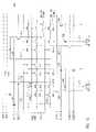
- FIG. 2a schematic diagram is depicted which represents a memory plane within an exemplary three-dimensional passive element memory array.
- the memory plane 150includes a plurality of blocks, such as blocks 151 , 152 , and 153 .
- Each blockincludes a plurality of word lines, such as word lines 156 associated with block 152 .
- Each blockalso includes a plurality of bit line segments, such as bit line segments 157 , 158 , 159 , and 160 associated with block 152 .
- a memory celle.g., memory cell 173
- Each bit line segmentmay be coupled to an associated global bit line by a segment switch device which is controlled by a block select signal.
- bit line segment 157is coupled by a segment switch device 161 to global bit line 154 , which preferably resides on a different layer of the memory array.
- the connection path to the global bit lineis formed by way of a vertical connection 167 , which is shared by other memory planes, to provide a path for a bit line segment from any of at least two memory planes to be coupled to the global bit line.
- bit line segments of memory plane 150are arranged in a 2:1 interleaved configuration, which allows the required pitch of the global bit lines to be twice that of the bit line segments.
- half of the bit line segments within a blockexit to the top of the block and are coupled under control of a SELECT-A control signal to the respective global bit lines, while the other half of the bit line segments exit to the bottom of the block and are coupled under control of a SELECT-B control signal to the same respective global bit lines.
- bit line segment 158is coupled by segment switch device 163 to a shared vertical connection 169 to global bit line 154
- bit line segment 159is coupled by segment switch device 162 to a shared vertical connection 168 to global bit line 155
- bit line segment 160is coupled by segment switch device 164 to a shared vertical connection 170 to global bit line 155 .
- each of the shared vertical connections(which are shared vertically with other memory planes) is also shared by a bit line segment in an adjacent memory block within the same memory plane.
- a bit line segment in block 151(unlabeled) is coupled by segment switch device 171 (under control of a block select signal SELECT-E) to the same shared vertical connection 167 , and consequently to global bit line 154 .
- SELECT-Eblock select signal
- bit line segment in block 151is coupled by segment switch device 172 (controlled by SELECT-E) to the shared vertical connection 168 , and consequently to global bit line 155 .
- segment switch device 172controlled by SELECT-E
- bit line segments from memory block 153are respectively coupled by segment switch devices 165 , 166 to shared vertical connections 169 , 170 and consequently to global bit lines 154 , 155 .
- each global bit lineis operably coupled to a respective bit line segment in a selected block of a selected memory plane by driving one of the two block select control signals associated with the selected block to an active state, while leaving the other block select control signal of the selected block, and all other blocks (both on the same memory plane and on other memory planes sharing the same global bit lines), at an inactive level.
- the signal from a memory cellis coupled from the bit line segment to a global bit line, and subsequently to sensing circuitry.
- the programming voltages and currentsare conveyed from write driver circuitry, through the global bit line, through the segment switch device to the bit line segment, and coupled thereby to the selected memory cell.
- FIG. 3Aa schematic diagram is depicted which represents a memory plane within an exemplary three-dimensional NOR EEPROM memory array. Again, only one such memory plane 200 is shown, although preferably other memory planes are similarly arranged and share the vertical connections to global bit lines.
- the memory plane 200includes a plurality of blocks, although only one such block is fully depicted (with select devices for another block drawn in dashed lines).
- Each blockincludes a plurality of word lines, such as word lines 216 , and also includes a plurality of bit line segments, such as bit line segments 201 , 202 , 203 , and 204 .
- Each blockalso includes a plurality of bias line segments, such as bias line segments 221 , 222 , 223 , and 224 .
- a memory celle.g., memory cell 215
- Such three-terminal memory cellsmay be viewed as including a switch device, and may advantageously include a device having a charge storage dielectric, such as a SONOS (silicon-oxide-nitride-oxide-silicon) device.
- SONOSsilicon-oxide-nitride-oxide-silicon
- such SONOS devicesmay include those having an oxynitride layer rather than, or in addition to, a nitride layer.
- Each bit line segmentmay be coupled to an associated global bit line by a segment switch device which is controlled by an associated block select signal.
- bit line segment 201is coupled by a segment switch device 205 (controlled by a SELECT-A block select signal) to global bit line 211 , which preferably resides on a different layer of the memory array.
- the connection path to the global bit lineis formed by way of a vertical connection 209 , which is shared by other memory planes, to provide a path for a bit line segment from any of at least two memory planes to be coupled to the associated global bit line.
- bit line segments of memory plane 200are arranged in a 2:1 interleaved configuration, which again allows the required pitch of the global bit lines to be twice that of the bit line segments.
- adjacent bit line segments within a blockshare the same vertical connection to a global bit line but are controlled by different block select signals.
- bit line segment 202is coupled by segment switch device 206 (controlled by a SELECT-B block select signal) to global bit line 211
- bit line segment 203is coupled by segment switch device 207 (controlled by SELECT-A) to global bit line 212
- bit line segment 204is coupled by segment switch device 208 (controlled by SELECT-B) similarly to global bit line 212 .
- the vertical connectionsmay also be shared by an adjacent block.
- segment switch device 213which is controlled by a block select signal SELECT-A′ (which is different from SELECT-A), couples a bit line segment from the adjacent memory block to the same vertical connection 209 to connect to the global bit line 211 .
- segment switch device 214(controlled by a block select signal SELECT-B′) couples another bit line segment from the adjacent memory block to the same vertical connection 209 to connect to the global bit line 211 .
- each vertical connection to an associated global bit lineis shared by two laterally adjacent bit line segments within each of two adjacent memory blocks within a bit line layer.
- Such vertical connectionsare also preferably shared by similar structures on one or more additional bit line layers of the array.
- each of the bias line segments within the blockis coupled by one of two bias line select signals associated with the block to a bias node for the block.
- bias line segment 221is coupled by segment switch device 217 (controlled by SELECT-C) to a common bias line 220
- bias line segment 222is coupled by segment switch device 218 (controlled by SELECT-D) to the same bias line 220 , both by way of a shared vertical connection 219 .
- the vertical connection 219(and consequently the bias line 220 ) may be shared by an adjacent block (not shown).
- the bias line 220is preferably routed on an interconnect layer above the memory cells, and traverses parallel to the word lines.
- the SELECT-C signalis connected to both device 217 and 218 but two different bias lines are provided.
- the arrangement of vertical connections to global bias lines and global bit linesis such that memory segments such as 221 and 222 that share a global bit line 211 do not share the same global bias line but rather are connected to bias line 241 and 242 , respectively.
- Shared vertical connections, such as 240for the connection to global bias lines may still be used to save area.
- each blockmay contain 128 word lines, and consequently there are 128 memory cells coupled to each bit line segment which together form a NOR group of memory cells.
- the bit line segmentsmay also be viewed as a segmented sense line or common source line of the memory cells of the block.
- there are many groups of 128 SONOS devices(alternatively, floating gate devices) that all share the 128 word lines (e.g., word lines 216 ) that form the gates of the SONOS devices, although in FIG. 3A only four such groups are shown.
- FIG. 3AIn the bit line direction, while two memory blocks are suggested by FIG. 3A , in practice it is anticipated that many such memory blocks would be present on each memory plane and share the same global bit lines.
- a number of memory planesare also contemplated, each sharing the same vertical connections to the global bit lines.
- eight memory planesi.e., memory layers
- other numbersboth greater and less than eight are also contemplated.
- numbers of memory planes which are integral powers of twomay be convenient for decoder efficiency, such is not necessarily required.
- the segment switch devicesmay be implemented as any of a variety of switch devices, such as MOS transistors, which may be N-channel, P-channel, enhancement mode or depletion mode, but are preferably implemented as a single device with the same structure as the SONOS memory cell devices.
- the width and length of the segment switch devicesare not necessarily the same as the cell device. In some embodiments the device may be about twice as wide as the cell device so the resistance of the device is smaller than the cell and has a minimal effect on the sensing operations.
- the threshold voltage (V T ) of the segment switch devicecan change during memory operation, particularly during program operations. Consequently, the segment switch device is preferably periodically biased in a suitable manner to periodically reset the V T to the low (i.e., erased) state. In some embodiments it may be desirable to modify the switch device to prevent such unintentional programming from occurring. For example, the semiconductor process may be altered to selectively remove the nitride region from the gate dielectric of the segment switch devices (but not the memory cell devices) before the transistor gate regions are formed. In an alternative embodiment, the segment switch is set to the high threshold value (i.e., programmed state) and the voltages applied to the various SELECT signals are high enough to pass the desired voltage and current.
- the high threshold valuei.e., programmed state
- the vertical connections to the global bit linesare shared by all eight memory planes.
- the vertical connectionsmay also be shared by two adjacent NOR groups (i.e., shared by two adjacent bit line segments).
- the individual bit line segmentsmay be individually coupled to the global bit lines to either sense the segmented lines one at a time or write the segmented lines one at a time.
- the vertical connectionsmay also be shared by an adjacent memory block, such as that selected by the SELECT-A′ and SELECT-B′ signals shown. This sharing reduces the number of vertical connections which take up valuable chip area, especially as the number of cells on the segment is frequently limited by program disturb characteristics and by the desired erase block size to be in the range of 128 cells or less.
- a number of memory blockssuch as 64 such memory blocks, may be provided, which all share the same global bit lines.
- the vertical connections from the bit line segments (through the segment switch devices) to a global sense linemay be shared between adjacent memory blocks, giving rise to, for example, 32 such vertical connections per global bit line.
- Each global bit lineis also connected to sense circuitry and a write drive (i.e., programming) circuitry, and in some embodiments also to a set of cells used as a reference for sensing.
- the global bit linestraverse parallel to the segmented sense lines (i.e., bit line segments) on a wiring layer preferably below the memory cells for easy attachment to support circuits.
- each global bit lineis coupled to a respective bit line segment in a selected block of a selected memory plane by driving one of the two block select control signals associated with the selected block to an active state, while leaving the other block select control signal of the selected block, and all the block select control signals of other blocks (both on the same memory plane and on other memory planes sharing the same global bit lines), at an inactive level.
- the signal from a memory cellis coupled from the bit line segment to a global bit line, and subsequently to sensing circuitry.
- the programming voltages and currentsare conveyed from write driver circuitry, through the global bit line, through the segment switch device to the bit line segment, and coupled thereby to the selected memory cell.
- control signals SELECT-A and SELECT-B and the control signals SELECT-C and SELECT-Dare coordinated so either a bit line segment select device (i.e., a bit line switch) or a bias line segment select device (i.e., a bias line switch) is on for each of the selected groups, but not both.
- the bias line 220is preferably utilized to provide a write inhibit voltage to unselected cell groups, as is further described in U.S. patent application Ser. No. 10/325,737, filed Dec. 23, 2002, entitled “Array Containing Charge Storage and Dummy Transistors and Method of Operating the Array,” which application is hereby incorporated by reference in its entirety.
- Some of the global bit linespreferably are biased to also provide a write inhibit voltage to other memory cell groups that are not being programmed.
- the SELECT-A, SELECT-B, SELECT-C, and SELECT-D control signalsare coordinated so that a suitable bias is supplied to the bias line side of a selected memory cell, and the bit line segment (sense line) switch device is turned on for sensing.
- FIG. 4is a schematic diagram representing a memory plane within an exemplary three-dimensional DRAM memory array. Only one such memory plane 250 is shown, although preferably other memory planes are similarly arranged and share the vertical connections to global bit lines.
- the memory plane 250includes a plurality of blocks, although only one such block is fully depicted (with select devices for another block drawn in dashed lines).
- Each blockincludes a plurality of word lines, such as word lines 266 and also includes a plurality of bit line segments, such as bit line segments 251 , 252 , 253 , and 254 .
- Each blockalso includes a plurality of bias line segments, such as bias line segments 271 , 272 , 273 , and 274 , which are connected to a common bias line 267 .
- a memory celle.g., memory cell 265
- Such three-terminal memory cellsmay be viewed as including a switch device, and may be formed in a variety of suitable configurations, but preferably include an enhancement mode NMOS select device in series with a dielectric capacitor.
- dielectricsmay include silicon oxides, silicon oxy-nitrides, tantalum oxides, and other desirable high permittivity dielectrics.
- each bit line segmentis coupled to an associated global bit line by a segment switch device which is controlled by an associated block select signal.
- bit line segment 251is coupled by a segment switch device 255 (controlled by a SELECT-A block select signal) to global bit line 261 , which resides on a different layer of the memory array.
- the connection path to the global bit lineis formed by way of a vertical connection 259 , which is shared by other memory planes, to provide a path for a bit line segment from any of at least two memory planes to be coupled to the associated global bit line.
- bit line segments of memory plane 250are arranged in a 2:1 interleaved configuration, which provides for the global bit line pitch to be twice that of the bit line pitch.
- bit line segment 252is coupled by segment switch device 256 (controlled by a SELECT-B block select signal) to global bit line 261 .
- bit line segment 253is coupled by segment switch device 257 (controlled by SELECT-A) to global bit line 262
- bit line segment 254is coupled by segment switch device 258 (controlled by SELECT-B) similarly to global bit line 262 , both by way of a shared vertical connection 260 .
- the shared vertical connectionsmay also be shared by an adjacent block within the same memory plane.
- segment switch device 263controlled by a block select signal SELECT-C, couples a bit line segment from the adjacent memory block to the same vertical connection 259 to connect to the global bit line 261 .
- segment switch device 264controlled by a block select signal SELECT-D, couples another bit line segment from the adjacent memory block to the same vertical connection 259 to connect to the global bit line 261 .
- each vertical connection to an associated global bit lineis shared by two laterally adjacent bit line segments within each of two adjacent memory blocks within a bit line layer.
- Such vertical connectionsare also preferably shared by similar structures on one or more additional bit line layers of the array.
- Each of the bias line segments within the blockis connected to a common bias line 267 , which is preferably routed parallel to the word lines on an interconnect layer above the memory cells, and may be shared with an adjacent memory block on the same memory plane, as well as shared by other memory planes through one or more vertical connections (not shown).
- the number of memory cells per bit line segmentmay be determined by the capacitance of the bit line segment compared to the global bit line. In some embodiments, 128 such memory cells may be associated with each bit line segment.
- the bit line segment switch devices(e.g., device 255 ) may be implemented as any of a variety of switch devices, such as MOS transistors, which may be N-channel, P-channel, enhancement mode or depletion mode, but are preferably implemented as a single device with the same or similar structure as the memory cell select devices. However, the width and length of the segment switch devices are not necessarily the same as the memory cell select device.
- DRAM memory cellsare destructively read, as is well known, and must be refreshed after being read.
- one of the word lines 266is driven to an active level, which transfers charge from the associated memory cells to both bit line segments 251 and 252 .
- the SELECT-A or SELECT-B control signalsBy first activating only one of the SELECT-A or SELECT-B control signals, one of the two bit line segments is coupled to the global bit line and may be sensed, then the global bit line is biased again at a suitable read level, and the other SELECT-A or SELECT-B control signal is then activated to couple the other bit line segment to the global bit line for sensing.
- the SELECT-C and SELECT-D control signalsremain inactive during such a read operation for the memory block shown, as do the associated control signals for all other blocks (both on the same memory plane and on other memory planes sharing the same global bit lines).
- the global bit lineis driven to a first data level for the first bit line segment sharing the global bit line, and the appropriate SELECT control signal is pulsed to write the data onto the first bit line segment (and into the selected memory cell), then the global bit line is driven to a second data level for the second bit line segment sharing the global bit line, and the other SELECT control signal is pulsed to write the data onto the second bit line segment.
- the selected word linemay then be inactivated to complete the write into the memory cells associated with the selected word line.
- FIG. 5a schematic diagram is depicted which represents a memory plane 300 within an exemplary three-dimensional FeRAM memory array, although preferably other memory planes are similarly arranged and share the vertical connections to global bit lines.
- the memory plane 300includes a plurality of blocks, although only one such block is fully depicted (with select devices for another block drawn in dashed lines).
- Each blockincludes a plurality of word lines, such as word lines 316 and also includes a plurality of bit line segments, such as bit line segments 301 , 302 , 303 , and 304 .
- Each blockalso includes a plurality of bias line segments, such as bias line segments 321 , 322 , 323 , and 324 .
- a memory cell(e.g., memory cell 315 ) is formed between a bit line segment and a bias line segment within a block, and is controlled by a world line within the block.
- Such three-terminal memory cellsmay be viewed as including a switch device, and may advantageously include an N-channel enhancement-mode field effect transistor.
- Each bit line segmentmay be coupled to an associated global bit line by a segment switch device which is controlled by an associated block select signal.
- the bit line segments of memory plane 300are arranged in a 2:1 interleaved configuration, which again allows the required pitch of the global bit lines to be twice that of the bit line segments. In this particular interleave arrangement adjacent bit line segments within a block share the same vertical connection to a global bit line but are controlled by different block select signals.
- bit line segments 301 , 302are respectively coupled by segment switch devices 305 (controlled by a SELECT-A) and 306 (controlled by SELECT-B), to the global bit line 311 by way of a shared vertical connection 309 , which is shared by other memory planes and optionally shared with an adjacent memory block (e.g., segment switch devices 313 , 314 ).
- Bit line segments 303 , 304are respectively coupled by segment switch devices 307 (controlled by SELECT-A) and 308 (controlled by SELECT-B) to a global bit line 312 by way of a shared vertical connection 310 , which is shared by other memory planes.
- each of the bias line segments within the blockis coupled by one of two bias line select signals associated with the block to a corresponding one of two bias nodes for the block.
- bias line segments 321 , 322are respectively coupled by segment switch devices 317 (controlled by SELECT-C), 318 (controlled by SELECT-D) to a bias line 319 , which is preferably routed on an interconnect layer above the memory cells and traverse parallel to the word lines.
- the bias line 319may be shared by an adjacent block (not shown).
- Memory blocksmay be configured with a number of word lines, such as 128 word lines, and many such memory blocks would preferably be present on each memory plane and share the same global bit lines.
- a number of memory planesare also contemplated, each sharing the same vertical connections to the global bit lines.
- a number of memory planesmay be provided, such as eight memory planes.
- the segment switch devicesmay be implemented as any of a variety of switch devices, such as MOS transistors, which may be N-channel, P-channel, enhancement mode or depletion mode, but are preferably implemented as a single device with the same structure as the memory cell switch devices.
- the width and length of the segment switch devicesare not necessarily the same as the cell device. In some embodiments the device may be about twice as wide as the cell device so the resistance of the device is smaller than the cell and has a minimal effect on the sensing operations.
- the vertical connectionsmay be shared by two adjacent NOR groups (i.e., shared by two adjacent bit line segments which share the same word lines).
- the individual bit line segmentsmay be individually coupled to the global bit lines to either sense the segmented lines one at a time or write the segmented lines one at a time.
- the vertical connectionsmay also be shared by an adjacent memory block, such as that selected by the SELECT-A′ and SELECT-B′ signals shown.
- SELECT-A, SELECT-B, SELECT-C, and SELECT-D control signalsare coordinated so that a suitable bias is supplied to the bias line side of a selected memory cell, and the bit line segment (sense line) switch device is turned on for sensing.
- the cell device in cell 315is turned on and SELECT-A and SELECT-C are at an active level to apply a voltage across the ferro-electric capacitor in the cell that is sufficient to polarize the ferro-electric material.
- SELECT-A and SELECT-Care at an active level to apply a voltage across the ferro-electric capacitor in the cell that is sufficient to polarize the ferro-electric material.
- a destructive read mode of operationthe cell 315 is read by sensing the current produced by a reversing of the polarization in the ferro-electric material in cell 315 .
- the cell deviceis turned on and SELECT-C and SELECT-A are at the active level, and a voltage pulse is applied from the global bias line BIAS 1 through device 317 to the segmented bias line 321 while sensing global bit line 311 .
- the SELECT-B and SELECT-D control signalsare at an inactive level, devices 306 and 318 are off, and no memory cell on bit line segment 302 receives a bias pulse either from the bias line or due to voltage transients on the bit line.
- known non-destructive read modes of operation of the FeRAM cellmay be used.
- FIG. 6is a perspective view of a multi-level array structure in accordance with an embodiment of the present invention, showing a half-mirrored memory array having bit line segments on a bit line layer shared with word lines on a first word line layer below the bit line layer and also by word lines on a second word line layer above the bit line layer.
- the labeling of this figuregenerally corresponds to that shown in FIG. 2 , assuming that the word lines 156 lie on a word line layer above the bit line layer containing bit line segments 157 , 158 , 159 , and 160 .
- the structure shown in FIG. 6includes a second word line layer which shares the same bit line layer.
- Word lines 352 on word line layer 1 and the bit lines 157 , 158 of bit line layer 2form another memory plane having a plurality of memory cells, such as memory cell 353 , each formed between an associated one of the word lines 352 and an associated on of the bit line segments on bit line layer 2 .
- the vertical connections 167 , 169provide for a connection path from the segment switch devices 161 , 163 (i.e., block select devices) within bit line layer 2 to an associated global bit line 154 .
- these vertical connections 167 , 169may provide a connection to additional bit line layers, as well.
- Such vertical connectionsmay be formed using one or more vias through the various layers of the integrated circuit, and may use vias having some degree of offset for successive vias, preferably the vertical connections are formed using substantially aligned or coincident via structures to reduce the total area consumed by such connections.
- This configurationrepresents bit line segments which are 2:1 interleaved, and thus allows a more relaxed global bit line pitch relative to the pitch of the bit line segments.
- FIG. 7a schematic diagram is depicted representing a bit line layer within an exemplary three-dimensional memory array 400 , illustrating non-interleaved bit line segments which do not share vertical connections with any other bit line segments on the same bit line layer.
- a bit line segment 404is coupled by segment switch device 403 to a vertical connection 405 , which is connected to global bit line 406 .
- a bit line segment 407is coupled by segment switch device 408 to a vertical connection 409 , which is also connected to global bit line 406 .
- the pitch of the global bit linesis identical to that of the bit line segments, and the pitch of the vertical connections is also identical to that of the bit line segments.
- a single block select signal(e.g., SELECT-A, SELECT-B) is provided for each array block.
- FIG. 8is a schematic diagram representing a bit line layer within an exemplary three-dimensional memory array 430 , illustrating 2:1 interleaved bit line segments, with a bit line segment from each of two adjacent blocks (i.e., opposing bit line segments) sharing a vertical connection to an associated global bit line, to achieve a global bit line pitch that is twice the pitch of the bit line segments.
- a bit line segment 434is coupled by segment switch device 439 to a vertical connection 440 , which is connected to global bit line 441 .
- the adjacent bit line segment 435is coupled by segment switch device 436 to a vertical connection 437 , which is also connected to the same global bit Line 441 .
- the vertical connection 440is also shared by a bit line segment within the adjacent array black 431 , white the vertical connection 437 is also shared by a bit line segment within adjacent array block 433 by way of segment switch device 438 .
- the pitch of global bit lines 441 , 442is twice that of the bit line segments 434 , 435 .
- the pitch of the vertical connections(e.g., vertical connections 440 , 443 ) is also twice that required by the structure of FIG. 7 .
- a pair of block select signalsis provided for each array block (e.g., SELECT-B, SELECT-C for block 432 ).
- FIG. 9is a schematic diagram representing a bit line layer within an exemplary three-dimensional memory array, illustrating 2:1 interleaved bit line segments, with two laterally adjacent bit line segments within the same block sharing a vertical connection to a global bit line with two laterally adjacent bit line segments within an adjacent block.
- a bit line segment 465is coupled by segment switch device 469 to a vertical connection 471 , which is connected to global bit line 474 .
- the adjacent bit line segment 466is coupled by segment switch device 470 to the same vertical connection 471 .
- bit line segment 467is coupled by segment switch device 472 to the same vertical connection 471
- bit line segment 468is coupled by segment switch device 473 to the same vertical connection 471 .
- Each vertical connectionis shared by a respective pair of adjacent bit line segments in each of two adjacent array blocks.
- the global bit line pitchis again twice the pitch of the bit line segments, as is the pitch of the vertical connections.
- Half as many vertical connectionsare needed relative to the structure of FIG. 8 , as no vertical connections are provided between array blocks 461 and 462 , and between array blocks 463 and 464 .
- a pair of block select signalsis provided for each array block (e.g., SELECT-A, SELECT-B for block 462 ), both disposed to one side of the array block.
- FIG. 10is a schematic diagram representing a bit line layer within an exemplary three-dimensional memory array, illustrating 2:1 interleaved bit line segments, with two laterally adjacent bit line segments within the same block sharing a vertical connection to a global bit line.
- a bit line segment 503is coupled by segment switch device 505 to a vertical connection 506 , which is connected to global bit line 508 .
- An adjacent bit line segment 504is coupled by segment switch device 507 to the same vertical connection 506 .
- a pair of bit line segmentsshares a vertical connection 509 , which connects to the same global bit line 508 .
- Each vertical connectionis shared by a pair of adjacent bit line segments within an array block.
- the global bit line pitch(and the vertical connection pitch) is again twice the pitch of the bit line segments.
- a pair of block select signalsis provided for each array block (e.g., SELECT-A, SELECT-B for block 501 ), both disposed to one side of the array block.
- FIG. 11is a schematic diagram representing a bit line layer within an exemplary three-dimensional memory array, illustrating 4:1 interleaved bit line segments, with two bit line segments within the same block sharing a vertical connection to a global bit line with two bit line segments within an adjacent block, to achieve a global bit line pitch that is one-fourth the pitch of the bit line segments.
- a bit line segment 536is coupled by segment switch device 538 to a vertical connection 540 , which is connected to global bit line 544 .
- An adjacent bit line segment 535is coupled by segment switch device 539 to the same vertical connection 540 .
- a pair of bit line segmentsare coupled through respective segment switch devices to the same vertical connection 540 .
- bit line segment 534is coupled by segment switch device 543 to a vertical connection 541 , which is similarly connected to global bit line 544 .
- Another bit line segment 537is coupled by segment switch device 542 to the same vertical connection 541 .
- another pair of bit line segmentsare coupled through respective segment switch devices to the same vertical connection 541 .
- Each vertical connectionis shared by a respective pair of adjacent bit line segments in each of two adjacent array blocks. But in this structure, the vertical connections are provided between each array block, allowing four bit line segments on the same bit line layer within a given array block to be associated with the same global bit line.
- the global bit line pitchis thus four times the pitch of the bit line segments, as is the pitch of the vertical connections. Since each vertical connection supports four bit line segments, no additional vertical connections are needed relative to the structure of FIG. 9 , but the required global bit line has nonetheless been relaxed by another factor of two.
- a quad of block select signalsis provided for each array block (e.g., SELECT-C, SELECT-D, SELECT-E, SELECT-F for block 532 ), disposed in pairs to each side of the array block.
- bit line segment 601are associated with bit line segment 601 .
- Memory cell devicesexist at every intersection of a word line and a gap between bit line segments 601 , 602 , 603 , and 604 and bias line segments 621 , 622 , 623 , and 624 .
- This arrangementforms a very dense matrix of memory cells in each memory layer and creates what could be called a cross-point device matrix of 4F 2 cells.
- a conductive path through a memory cell 615 from BIAS 1 line 620 to the global bit line 611is established by raising SELECT-C and SELECT-A to their active level and raising the word line 616 .
- the path through memory cell 625requires SELECT-D and SELECT-A to be active. While sensing memory cell 615 , a potential sneak path through collective devices 618 , 627 , 626 , and 625 to bit line segment 601 may exist. But this potential sneak path does not interfere with sensing if the BIAS 2 line 619 is held at a voltage close to the voltage of the global bit line 611 . Current mode sensing on global bit lines is preferred for this embodiment.
- the BIAS 1 and BIAS 2 linesare respectively coupled to alternating pairs of bias line segments.
- BIAS 1is coupled to bias line segment 621 (by SELECT-C) and bias line segment 622 (by SELECT-D), whereas BIAS 2 is coupled to bias line segment 623 (by SELECT-C) and bias line segment 624 (by SELECT-D).
- This embodimentis also envisioned with write-once memory cells.
- the global bit linesmay reside on a layer that is below all the memory layers (i.e., memory planes), above all the memory layers, or in the midst of the memory layers.
- the global bit linesmay reside on more than one layer.
- a first layer of global bit linesmay be associated with some of the memory planes, and second layer of global bit lines may be associated with the remaining memory planes.
- a memory cellis connected between an associated bit line segment and an associated word line.
- each memory cellis also connected to an associated bias line segment.
- Such a bias line segmentmay include a bias segment switch device providing a connection to an associated bias line.
- Such bias linespreferably run perpendicular to the sensing lines (i.e., the global bit lines).
- segment switch devicesfor one or both of the bit line segment and bias line segments
- such segment switch devicesmay be formed by the same process steps as the array device. This both simplifies the process flow and may also result in a smaller layout, as the space between an array device and a segment switch device need not accommodate a mask tolerance to selectively process one differently than the other.
- the segment switch devicemay be formed differently than the switch device (if present) within the memory cell, and so would have different characteristics than the memory cell switch device.
- a memory arraymay include passive element memory cells, DRAM-like memory cells, or FeRAM (Ferro-electric RAM) memory cells.
- Such memory cellsmay be formed on a segmented bit line (i.e., each memory cell coupled to an associated bit line segment) on one or more layers of a memory array.
- the vertical connectionsmay connect to a single bit line segment on a layer, or may be shared by more than one bit line segment on a layer.
- a respective bit line segment in each of two adjacent array blocksi.e., they are associated with different word lines
- two (or more) bit line segments in the same array blocki.e., they are associated with the same word lines
- Such sharingallows the global bit line pitch and vertical connection pitch to be at least twice the bit line segment pitch, which is particularly advantageous for small memory cells such as Flash EEPROM cells (e.g., floating gate or SONOS type) and passive element memory cells.
- a single layer of global bit linesis provided.
- This global bit line layermay be above, within, or below the memory planes, although providing the global bit line layer below the memory array allows more advantageous routing to bit line circuitry such as drivers and sense amplifiers.
- two layers of global bit linesmay be provided, such as one layer below the memory planes and the other layer above the memory planes.
- one bit line segment of an adjacent pair of bit line segmentsi.e., sharing the same word lines
- the second bit line segment of the adjacent pairis associated with the second global bit line layer, which allows an even larger global bit line pitch on each global bit line layer.
- the bit line circuitrycan be located below some of the array blocks.
- the array blockscan be grouped into multiple sub-arrays.
- the bit line circuitryis located under only some of the sub-arrays in the manner of a checkerboard array, as described in U.S. patent application Ser. No. 09/896,814, filed Jun. 29, 2001, entitled “Memory Device With Row and Column Decoder Circuits Arranged in a Checkerboard Pattern Under a Plurality of Memory Arrays,” which application is hereby incorporated by reference in its entirety.
- a checkerboard arrangementis also envisioned for any of the embodiments described herein.
- the global bit linesmay be extended to the edge of some of the sub-arrays to reach and share bit line circuitry placed under an adjacent sub-array. Circuitry that controls the word lines lies below the global bit lines in others of the sub-arrays.
- memory layersmay be formed as a mirrored structure so that bit lines (i.e., bit line segments) and/or word lines are shared by more than one memory plane.
- a half-mirrored memory arraymay include word lines within a word line layer which are shared by a first bit line layer disposed above the word line layer and by a second bit line layer disposed below the word line layer, with the first and second bit line layers not shared with other word line layers.
- another exemplary half-mirrored memory arraymay include bit line segments within a bit line layer which are shared by a first word line layer disposed above the bit line layer and by a second word line layer disposed below the bit line layer, with the first and second word line layers not shared with other bit line layers.
- two global bit line layersmay be provided so that one memory layer is associated with the first global bit line layer, and another memory layer is associated with the second global bit line layer.
- the upper bit line layermay be associated with the first global bit line layer while the lower bit line layer may be associated with the second global bit line layer.
- a first set of bit line layersmay be associated with the first global bit line layer, with a second set of bit line layers associated with the second global bit line layer.
- a half-mirrored memory arraymay include two sets of memory layers corresponding respectively to two global bit line layers.
- the segment switch devicesmay be implemented as diodes functioning as isolation devices. If the bias voltage of a global bit line is maintained within a forward diode drop of a bit line segment, no substantial current will flow and the bit line segment remains substantially isolated from the global bit line. A selected bit line segment may be biased at a voltage different enough from the global bit line voltage to turn on the isolation diode and provide a conduction path to the global bit line for sensing.
- Table 1various contemplated embodiments are indicated, in which table “P” indicates a preferred embodiment, “A” indicates applicability, “L” indicates lower likelihood of application, and “X” indicates no probable advantage and likely, but not necessarily, even lower applicability.
- the connections between memory layersare advantageously formed as a vertical connection to reduce the overall area consumed by such connections.
- vertical connectionshould be interpreted to include any manner of making a connection between vertically adjacent memory layers, whether using a separate via to connect each layer to it neighboring layer, whether such vias are stacked one atop another, whether each via is laterally displaced relative to the vias above and below it, or whether any other structure is used to fashion a connection between nodes on more than one memory layer.
- the inventionis not limited to any particular form of “vertical connection,” as different processes may result in more or less desirable choices for each process.
- ziaSuch a vertical connection may also be conveniently termed a “zia” to imply a via-type structure connecting more than one layer in the z-direction.
- Preferred zia structuresare described in U.S. Pat. No. 6,534,403 to Cleeves, issued Mar. 18, 2003, the disclosure of which is hereby incorporated by reference in its entirety.
- a number of memory cells per bit line segmenthas been assumed for convenience of description. It should be understood that, as with any memory array design, a number of factors may influence design decisions as to the number of memory cells per bit line segment. For example, the number of memory cells per bit line segment may be heavily influenced by the total leakage current which may affect a selected or unselected bit line segment, by resistance of the bit line segment and/or global bit line, or by capacitance of the bit line segment and/or global bit line. Similarly, the number of array blocks, the number of memory planes, and the number of global bit line layers are also a matter of engineering decision, and the exemplary configurations described herein are only examples of selected cases and not required configurations.
- the capacitance per unit length of the global bit lineis preferably lower than that of the bit line segments because the global bit line does not bear the capacitance of unselected bit line segments, and thus the overall capacitance of the bit line during sensing is reduced because only one of the many segmented bit lines associated with a given column is coupled to the global bit line.
- the capacitance per unit length of the global bit lineis at least 5 times lower than that of a bit line segment.
- the overall resistance of the combined bit linemay also be reduced because the global bit line may be implemented having a larger pitch than the bit line segments, and also may be implemented using a lower resistance material than the usually much shorter segmented bit lines that may be implemented using a material having a relatively high resistance per unit length.
- the resistance per unit length of the global bit lineis at least 5 times lower than that of a bit line segment.
- different types of memory cellsmay be combined within the same three-dimensional memory array within a single monolithic integrated circuit device.
- One memory planemay include memory cells of a different type than another memory plane.
- a memory arraymay include Flash EEPROM memory cells on one or more levels, and single device ROM cells on one or more different levels.
- Passive element memory cell layersare envisioned in combination with at least one layer of diode-type ROM cells. Consequently, in certain embodiments of the invention, the various memory planes need not all have the same type of memory cell.
- an integrated circuit memory arrayis a monolithic integrated circuit structure, rather than more than one integrated circuit device packaged together or in close proximity.
- bit line segments on different layersmay include different numbers of memory cells
- the memory arraymay include three memory planes
- bit line segments within the first and last array blockmay be different in number of memory cells or global bit line configuration, and any of many other irregular variations to the usual consistency of memory array design.
- the segment switch devicesmay be formed using the same process flow as the memory cells to reduce the number of process steps and device structures fabricated at each memory level.
- the segment switch devicesare formed having the same structure as the memory cells, although they may be sized differently (e.g., larger in width).
- such segment switch devicesmay be considered to be structurally substantially identical to the memory cell devices, even though their respective threshold voltages may be programmed or erased to different values.
- the word lines for a blockmay be implemented as two inter-digitated groups of word lines oriented horizontally, and the global bit lines for a block may be implemented as two inter-digitated groups of global bit line oriented vertically.
- Each respective group of word lines or global bit linesmay be served by a respective decoder/driver circuit and a respective sense circuit on one of the four sides of the array.
- Suitable row and column circuitsare set forth in “Multi-Headed Decoder Structure Utilizing Memory Array Line Driver with Dual Purpose Driver Device,” U.S. patent application Ser. No. 10/306,887, filed Nov.
- Word linesmay also be referred to as row lines or X-lines, and bit lines may also be referred to as column lines or Y-lines.
- word linesmay carry at least two different connotations to those skilled in the art.
- X-linesor word lines
- Y-linesor bit lines
- X-linesare usually contemplated as being connected to the gate terminal of memory cell transistors, or the switch terminal of the memory cell switch device, if present.
- the Y-lines (or bit lines)are usually contemplated as being connected to a switched terminal of the memory cell (e.g., source/drain terminal).
- the memory organizatione.g., data bus width, number of bits simultaneously read during an operation, etc.
- the memory organizationmay have some association with viewing one set of the two array lines more aligned with data “bits” rather than data “words.” Consequently, the designations herein of X-lines, word lines, and row lines, and of Y-lines, bit lines, and column lines are illustrative of the various embodiments but should not be viewed in a restrictive sense, but rather a more general sense.
- a “global bit line”is an array line that connects to bit line segments in more than one memory block, but no particular inference should be drawn suggesting such a global bit line must traverse across an entire memory array or substantially across an entire integrated circuit.
- a passive element memory arrayincludes a plurality of 2-terminal memory cells, each connected between an associated X-line and an associated Y-line.
- Such a memory arraymay be a two-dimensional (planar) array or may be a three-dimensional array having more than one plane of memory cells.
- Each such memory cellhas a non-linear conductivity in which the current in a reverse direction (i.e., from cathode to anode) is lower than the current in a forward direction.
- Application of a voltage from anode to cathode greater than a programming levelchanges the conductivity of the memory cell.
- the conductivitymay decrease when the memory cell incorporates a fuse technology, or may increase when the memory cell incorporates an antifuse technology.
- a passive element memory arrayis not necessarily a one-time programmable (i.e., write once) memory array.
- Such passive element memory cellsmay generally be viewed as having a current steering element directing current in a direction and another component which is capable of changing its state (e.g., a fuse, an antifuse, a capacitor, a resistive element, etc.).
- the programming state of the memory elementcan be read by sensing current flow or voltage drop when the memory element is selected.
- the memory cellsmay be comprised of semiconductor materials, as described in U.S. Pat. No. 6,034,882 to Johnson et al., U.S. Pat. No. 5,295,396 to Zhang, U.S. patent application Ser. No. 09/560,116 by Knall, and U.S. patent application Ser. No. 09/638,428 by Johnson, each of which are hereby incorporated by reference. Specifically an antifuse memory cell is preferred.
- Other types of memory arrayssuch as MRAM and organic passive element arrays, may also be used.
- MRAMmagnetoresistive random access memory
- MRAMmagnetic tunnel junction
- MRAM technologyis described in “A 256 kb 3.0 V 1T1MTJ Nonvolatile Magnetoresistive RAM” by Peter K Naji et al., published in the Digest of Technical Papers of the 2001 IEEE International Solid-State Circuits Conference, ISSCC 2001/Session 7/Technology Directions: Advanced Technologies/7.6, Feb. 6, 2001 and pages 94–95, 404–405 of ISSCC 2001 Visual Supplement, both of which are hereby incorporated by reference.
- Certain passive element memory cellsincorporate layers of organic materials including at least one layer that has a diode-like characteristic conduction and at least one organic material that changes conductivity with the application of an electric field.
- Suitable memory cell structures and configurations useful for cross-point antifuse arraysinclude, without limitation, those described in: U.S. Pat. No. 6,034,882 to Johnson, et al, entitled “Vertically Stacked Field Programmable Nonvolatile Memory and Method of Fabrication”; U.S. patent application Ser. No. 09/814,727 by Knall, et al, filed Mar. 21, 2001, entitled “Three-Dimensional Memory Array and Method of Fabrication”; U.S. patent application Ser. No. 09/928,536 by Johnson, filed Aug.
- Suitable memory cell structures and configurations useful for other array embodimentsinclude, without limitation, those described in: U.S. patent application Ser. No. 09/927,648 by Lee, et al, filed Aug. 13, 2001, entitled “Dense Arrays and Charge Storage Devices, and Methods for Making Same”; U.S. patent application Ser. No. 10/180046 by Patel, et al, filed Jun. 27, 2002, entitled “High Density 3D Rail Stack Arrays and Method of Making”; U.S. patent application Ser. No. 10/325,951 by Ilkbahar, et al, filed Dec.
- nodemay actually represent a pair of nodes for conveying a differential signal, or may represent multiple separate wires (e.g., a bus) for carrying several related signals or for carrying a plurality of signals forming a digital word or other multi-bit signal.
- circuits and physical structuresare generally presumed, it is well recognized that in modern semiconductor design and fabrication, physical structures and circuits may be embodied in computer readable descriptive form suitable for use in subsequent design, test or fabrication stages as well as in resultant fabricated semiconductor integrated circuits. Accordingly, claims directed to traditional circuits or structures may, consistent with particular language thereof, read upon computer readable encodings and representations of same, whether embodied in media or combined with suitable reader facilities to allow fabrication, test, or design refinement of the corresponding circuits and/or structures.
- the inventionis contemplated to include circuits, related methods or operation, related methods for making such circuits, and computer-readable medium encodings of such circuits and methods, all as described herein, and as defined in the appended claims.
- a computer-readable mediumincludes at least disk, tape, or other magnetic, optical, semiconductor (e.g., flash memory cards, ROM), or electronic medium and a network, wireline, wireless or other communications medium.
- An encoding of a circuitmay include circuit schematic information, physical layout information, behavioral simulation information, and/or may include any other encoding from which the circuit may be represented or communicated.
Landscapes
- Semiconductor Memories (AREA)
- Dram (AREA)
Abstract
Description
| TABLE 1 | |||||
| Configuration: | |||||
| (may be used alone or | Flash | Passive | |||
| combined with others) | EEPROM | ROM | Element | DRAM | FeRAM |
| Segmented bit lines on N | P | P | P | P | P |
| layers, N segment | |||||
| switches, and a shared | |||||
| GBL | |||||
| Switch for Bias side of | P | L | X | A | P |
| cell through vertical | |||||
| connection to Line | |||||
| perpendicular to GBL | |||||
| Switch for Bias side of | A | P | X | A | A |
| cell through vertical | |||||
| connection to line | |||||
| parallel to GBL | |||||
| A vs. B segment switch | A | A | P | A | A |
| control for fewer GBLs | |||||
| A vs. B segment switch | P | P | X | A | P |
| control plus C vs. D bias | |||||
| switch control | |||||
| Segments not sharing a | P | P | P | P | P |
| word line share the | |||||
| vertical connection (zia) | |||||
| A vs. B on opposite ends | A | P | P | L | L |
| of interleaved segments | |||||
| for fewer GBLs | |||||
| Half the GBLs above and | A | A | P | A | A |
| half below | |||||
| Full mirrored memory | A | A | P | L | L |
| layers | |||||
| Half mirrored memory | A | P | A | A | A |
| layers | |||||
| Two sets of layers and | A | A | A | A | A |
| two vertical connections | |||||
| to two GBLs | |||||
| Mirrored and two sets | A | A | P | L | L |
| Virtual ground array | A | A | X | L | L |
Claims (37)
Priority Applications (4)
| Application Number | Priority Date | Filing Date | Title |
|---|---|---|---|
| US10/403,752US7233024B2 (en) | 2003-03-31 | 2003-03-31 | Three-dimensional memory device incorporating segmented bit line memory array |
| PCT/US2004/009756WO2004090905A2 (en) | 2003-03-31 | 2004-03-31 | Three-dimensional memory device incorporating segmented bit line memory array |
| US11/764,789US8659028B2 (en) | 2003-03-31 | 2007-06-18 | Three-dimensional memory device incorporating segmented array line memory array |
| US13/348,336US8637870B2 (en) | 2003-03-31 | 2012-01-11 | Three-dimensional memory device incorporating segmented array line memory array |
Applications Claiming Priority (1)
| Application Number | Priority Date | Filing Date | Title |
|---|---|---|---|
| US10/403,752US7233024B2 (en) | 2003-03-31 | 2003-03-31 | Three-dimensional memory device incorporating segmented bit line memory array |
Related Child Applications (1)
| Application Number | Title | Priority Date | Filing Date |
|---|---|---|---|
| US11/764,789ContinuationUS8659028B2 (en) | 2003-03-31 | 2007-06-18 | Three-dimensional memory device incorporating segmented array line memory array |
Publications (2)
| Publication Number | Publication Date |
|---|---|
| US20040188714A1 US20040188714A1 (en) | 2004-09-30 |
| US7233024B2true US7233024B2 (en) | 2007-06-19 |
Family
ID=32990020
Family Applications (3)
| Application Number | Title | Priority Date | Filing Date |
|---|---|---|---|
| US10/403,752Expired - LifetimeUS7233024B2 (en) | 2003-03-31 | 2003-03-31 | Three-dimensional memory device incorporating segmented bit line memory array |
| US11/764,789Active2026-04-14US8659028B2 (en) | 2003-03-31 | 2007-06-18 | Three-dimensional memory device incorporating segmented array line memory array |
| US13/348,336Expired - LifetimeUS8637870B2 (en) | 2003-03-31 | 2012-01-11 | Three-dimensional memory device incorporating segmented array line memory array |
Family Applications After (2)
| Application Number | Title | Priority Date | Filing Date |
|---|---|---|---|
| US11/764,789Active2026-04-14US8659028B2 (en) | 2003-03-31 | 2007-06-18 | Three-dimensional memory device incorporating segmented array line memory array |
| US13/348,336Expired - LifetimeUS8637870B2 (en) | 2003-03-31 | 2012-01-11 | Three-dimensional memory device incorporating segmented array line memory array |
Country Status (2)
| Country | Link |
|---|---|
| US (3) | US7233024B2 (en) |
| WO (1) | WO2004090905A2 (en) |
Cited By (100)
| Publication number | Priority date | Publication date | Assignee | Title |
|---|---|---|---|---|
| US20070008773A1 (en)* | 2005-07-11 | 2007-01-11 | Matrix Semiconductor, Inc. | Nonvolatile memory cell comprising switchable resistor and transistor |
| US20070263423A1 (en)* | 2003-03-31 | 2007-11-15 | Scheuerlein Roy E | Three-dimensional memory device incorporating segmented array line memory array |
| US20080025085A1 (en)* | 2006-07-31 | 2008-01-31 | Scheuerlein Roy E | Memory array incorporating two data busses for memory array block selection |
| US20080025134A1 (en)* | 2006-07-31 | 2008-01-31 | Scheuerlein Roy E | Method for using two data busses for memory array block selection |
| US20080025088A1 (en)* | 2006-07-31 | 2008-01-31 | Scheuerlein Roy E | Apparatus for reading a multi-level passive element memory cell array |
| US20080025089A1 (en)* | 2006-07-31 | 2008-01-31 | Scheuerlein Roy E | Method for reading a multi-level passive element memory cell array |
| US20080311722A1 (en)* | 2007-06-15 | 2008-12-18 | Sandisk 3D Llc | Method for forming polycrystalline thin film bipolar transistors |
| US20080308903A1 (en)* | 2007-06-15 | 2008-12-18 | Sandisk 3D Llc | Polycrystalline thin film bipolar transistors |
| US20090003109A1 (en)* | 2007-06-29 | 2009-01-01 | Tyler Thorp | Methods and apparatus for extending the effective thermal operating range of a memory |
| US20090080244A1 (en)* | 2007-09-17 | 2009-03-26 | Eric Carman | Refreshing Data of Memory Cells with Electrically Floating Body Transistors |
| US7542340B2 (en)* | 2006-07-11 | 2009-06-02 | Innovative Silicon Isi Sa | Integrated circuit including memory array having a segmented bit line architecture and method of controlling and/or operating same |
| US20090142921A1 (en)* | 2005-03-25 | 2009-06-04 | Sandisk 3D Llc | Method for reducing dielectric overetch when making contact to conductive features |
| US20090272960A1 (en)* | 2008-05-02 | 2009-11-05 | Bhaskar Srinivasan | Non-Volatile Resistive Oxide Memory Cells, and Methods Of Forming Non-Volatile Resistive Oxide Memory Cells |
| US20090316467A1 (en)* | 2008-06-18 | 2009-12-24 | Jun Liu | Memory Device Constructions, Memory Cell Forming Methods, and Semiconductor Construction Forming Methods |
| US20100046273A1 (en)* | 2007-06-22 | 2010-02-25 | Panasonic Corporation | Resistance change nonvolatile memory device |
| US20100085806A1 (en)* | 2008-10-02 | 2010-04-08 | Ping Wang | Techniques for reducing a voltage swing |
| US20100224924A1 (en)* | 2009-03-04 | 2010-09-09 | Innovative Silicon Isi Sa | Techniques for forming a contact to a buried diffusion layer in a semiconductor memory device |
| US20100271863A1 (en)* | 2008-01-15 | 2010-10-28 | Jun Liu | Memory Cells, Memory Cell Programming Methods, Memory Cell Reading Methods, Memory Cell Operating Methods, and Memory Devices |
| US20100297834A1 (en)* | 2005-03-25 | 2010-11-25 | Dunton Samuel V | Method for reducing dielectric overetch using a dielectric etch stop at a planar surface |
| US7924630B2 (en) | 2008-10-15 | 2011-04-12 | Micron Technology, Inc. | Techniques for simultaneously driving a plurality of source lines |
| US7933142B2 (en) | 2006-05-02 | 2011-04-26 | Micron Technology, Inc. | Semiconductor memory cell and array using punch-through to program and read same |
| US20110096588A1 (en)* | 2009-10-26 | 2011-04-28 | Fasoli Luca G | Non-volatile memory array architecture incorporating 1t-1r near 4f2 memory cell |
| US7940559B2 (en) | 2006-04-07 | 2011-05-10 | Micron Technology, Inc. | Memory array having a programmable word length, and method of operating same |
| US7947543B2 (en) | 2008-09-25 | 2011-05-24 | Micron Technology, Inc. | Recessed gate silicon-on-insulator floating body device with self-aligned lateral isolation |
| US7957206B2 (en) | 2008-04-04 | 2011-06-07 | Micron Technology, Inc. | Read circuitry for an integrated circuit having memory cells and/or a memory cell array, and method of operating same |
| US8014195B2 (en) | 2008-02-06 | 2011-09-06 | Micron Technology, Inc. | Single transistor memory cell |
| US8023307B1 (en) | 2010-04-30 | 2011-09-20 | Hewlett-Packard Development Company, L.P. | Peripheral signal handling in extensible three dimensional circuits |
| US8034655B2 (en) | 2008-04-08 | 2011-10-11 | Micron Technology, Inc. | Non-volatile resistive oxide memory cells, non-volatile resistive oxide memory arrays, and methods of forming non-volatile resistive oxide memory cells and memory arrays |
| US8064274B2 (en) | 2007-05-30 | 2011-11-22 | Micron Technology, Inc. | Integrated circuit having voltage generation circuitry for memory cell array, and method of operating and/or controlling same |
| US8069377B2 (en) | 2006-06-26 | 2011-11-29 | Micron Technology, Inc. | Integrated circuit having memory array including ECC and column redundancy and method of operating the same |
| US8085594B2 (en) | 2007-06-01 | 2011-12-27 | Micron Technology, Inc. | Reading technique for memory cell with electrically floating body transistor |
| US8139418B2 (en) | 2009-04-27 | 2012-03-20 | Micron Technology, Inc. | Techniques for controlling a direct injection semiconductor memory device |
| US20120075912A1 (en)* | 2010-09-24 | 2012-03-29 | Kabushiki Kaisha Toshiba | Nonvolatile semiconductor memory device |
| US8174881B2 (en) | 2009-11-24 | 2012-05-08 | Micron Technology, Inc. | Techniques for reducing disturbance in a semiconductor device |
| US8189376B2 (en) | 2008-02-08 | 2012-05-29 | Micron Technology, Inc. | Integrated circuit having memory cells including gate material having high work function, and method of manufacturing same |
| US20120140542A1 (en)* | 2010-12-02 | 2012-06-07 | Jun Liu | Arrays of Nonvolatile Memory Cells |
| US8199595B2 (en) | 2009-09-04 | 2012-06-12 | Micron Technology, Inc. | Techniques for sensing a semiconductor memory device |
| US8213226B2 (en) | 2008-12-05 | 2012-07-03 | Micron Technology, Inc. | Vertical transistor memory cell and array |
| US8223574B2 (en) | 2008-11-05 | 2012-07-17 | Micron Technology, Inc. | Techniques for block refreshing a semiconductor memory device |
| US8264041B2 (en) | 2007-01-26 | 2012-09-11 | Micron Technology, Inc. | Semiconductor device with electrically floating body |
| US8279704B2 (en) | 2006-07-31 | 2012-10-02 | Sandisk 3D Llc | Decoder circuitry providing forward and reverse modes of memory array operation and method for biasing same |
| US8310893B2 (en) | 2009-12-16 | 2012-11-13 | Micron Technology, Inc. | Techniques for reducing impact of array disturbs in a semiconductor memory device |
| US8315099B2 (en) | 2009-07-27 | 2012-11-20 | Micron Technology, Inc. | Techniques for providing a direct injection semiconductor memory device |
| US8319294B2 (en) | 2009-02-18 | 2012-11-27 | Micron Technology, Inc. | Techniques for providing a source line plane |
| US8349662B2 (en) | 2007-12-11 | 2013-01-08 | Micron Technology, Inc. | Integrated circuit having memory cell array, and method of manufacturing same |
| US8369177B2 (en) | 2010-03-05 | 2013-02-05 | Micron Technology, Inc. | Techniques for reading from and/or writing to a semiconductor memory device |
| US8411524B2 (en) | 2010-05-06 | 2013-04-02 | Micron Technology, Inc. | Techniques for refreshing a semiconductor memory device |
| US8411513B2 (en) | 2010-03-04 | 2013-04-02 | Micron Technology, Inc. | Techniques for providing a semiconductor memory device having hierarchical bit lines |
| US8411477B2 (en) | 2010-04-22 | 2013-04-02 | Micron Technology, Inc. | Arrays of vertically stacked tiers of non-volatile cross point memory cells, methods of forming arrays of vertically stacked tiers of non-volatile cross point memory cells, and methods of reading a data value stored by an array of vertically stacked tiers of non-volatile cross point memory cells |
| US8416636B2 (en) | 2010-02-12 | 2013-04-09 | Micron Technology, Inc. | Techniques for controlling a semiconductor memory device |
| US8427859B2 (en) | 2010-04-22 | 2013-04-23 | Micron Technology, Inc. | Arrays of vertically stacked tiers of non-volatile cross point memory cells, methods of forming arrays of vertically stacked tiers of non-volatile cross point memory cells, and methods of reading a data value stored by an array of vertically stacked tiers of non-volatile cross point memory cells |
| US8431458B2 (en) | 2010-12-27 | 2013-04-30 | Micron Technology, Inc. | Methods of forming a nonvolatile memory cell and methods of forming an array of nonvolatile memory cells |
| US8498157B2 (en) | 2009-05-22 | 2013-07-30 | Micron Technology, Inc. | Techniques for providing a direct injection semiconductor memory device |
| US8509025B2 (en) | 2006-07-31 | 2013-08-13 | Sandisk 3D Llc | Memory array circuit incorporating multiple array block selection and related method |
| US8508994B2 (en) | 2009-04-30 | 2013-08-13 | Micron Technology, Inc. | Semiconductor device with floating gate and electrically floating body |
| US8518774B2 (en) | 2007-03-29 | 2013-08-27 | Micron Technology, Inc. | Manufacturing process for zero-capacitor random access memory circuits |
| US8531878B2 (en) | 2011-05-17 | 2013-09-10 | Micron Technology, Inc. | Techniques for providing a semiconductor memory device |
| US8537610B2 (en) | 2009-07-10 | 2013-09-17 | Micron Technology, Inc. | Techniques for providing a semiconductor memory device |
| US8537592B2 (en) | 2011-04-15 | 2013-09-17 | Micron Technology, Inc. | Arrays of nonvolatile memory cells and methods of forming arrays of nonvolatile memory cells |
| US8536628B2 (en) | 2007-11-29 | 2013-09-17 | Micron Technology, Inc. | Integrated circuit having memory cell array including barriers, and method of manufacturing same |
| US8547738B2 (en) | 2010-03-15 | 2013-10-01 | Micron Technology, Inc. | Techniques for providing a semiconductor memory device |
| US8576631B2 (en) | 2010-03-04 | 2013-11-05 | Micron Technology, Inc. | Techniques for sensing a semiconductor memory device |
| US8614918B2 (en) | 2011-05-02 | 2013-12-24 | Micron Technology, Inc. | Memory apparatus and methods |
| US8619453B2 (en) | 2010-12-14 | 2013-12-31 | Sandisk 3D Llc | Three dimensional non-volatile storage with dual gate selection of vertical bit lines |
| US8681531B2 (en) | 2011-02-24 | 2014-03-25 | Micron Technology, Inc. | Memory cells, methods of forming memory cells, and methods of programming memory cells |
| US20140133231A1 (en)* | 2012-11-15 | 2014-05-15 | SanDisk Technologies, Inc. | Bit line resistance compensation |
| US8748959B2 (en) | 2009-03-31 | 2014-06-10 | Micron Technology, Inc. | Semiconductor memory device |
| US8753949B2 (en) | 2010-11-01 | 2014-06-17 | Micron Technology, Inc. | Nonvolatile memory cells and methods of forming nonvolatile memory cells |
| US8759809B2 (en) | 2010-10-21 | 2014-06-24 | Micron Technology, Inc. | Integrated circuitry comprising nonvolatile memory cells having platelike electrode and ion conductive material layer |
| US8766332B2 (en) | 2003-12-05 | 2014-07-01 | Sandisk 3D Llc | Optimization of critical dimensions and pitch of patterned features in and above a substrate |
| US8773933B2 (en) | 2012-03-16 | 2014-07-08 | Micron Technology, Inc. | Techniques for accessing memory cells |
| US8791447B2 (en) | 2011-01-20 | 2014-07-29 | Micron Technology, Inc. | Arrays of nonvolatile memory cells and methods of forming arrays of nonvolatile memory cells |
| US8811063B2 (en) | 2010-11-01 | 2014-08-19 | Micron Technology, Inc. | Memory cells, methods of programming memory cells, and methods of forming memory cells |
| US8873283B2 (en) | 2005-09-07 | 2014-10-28 | Micron Technology, Inc. | Memory cell and memory cell array having an electrically floating body transistor, and methods of operating same |
| US8976566B2 (en) | 2010-09-29 | 2015-03-10 | Micron Technology, Inc. | Electronic devices, memory devices and memory arrays |
| US9165933B2 (en) | 2013-03-07 | 2015-10-20 | Sandisk 3D Llc | Vertical bit line TFT decoder for high voltage operation |
| US9171584B2 (en) | 2012-05-15 | 2015-10-27 | Sandisk 3D Llc | Three dimensional non-volatile storage with interleaved vertical select devices above and below vertical bit lines |
| US9202694B2 (en) | 2013-03-04 | 2015-12-01 | Sandisk 3D Llc | Vertical bit line non-volatile memory systems and methods of fabrication |
| US9257136B1 (en) | 2015-05-05 | 2016-02-09 | Micron Technology, Inc. | Magnetic tunnel junctions |
| US9281044B2 (en) | 2013-05-17 | 2016-03-08 | Micron Technology, Inc. | Apparatuses having a ferroelectric field-effect transistor memory array and related method |
| US9299439B2 (en) | 2012-08-31 | 2016-03-29 | Micron Technology, Inc. | Erasable block segmentation for memory |
| US9343665B2 (en) | 2008-07-02 | 2016-05-17 | Micron Technology, Inc. | Methods of forming a non-volatile resistive oxide memory cell and methods of forming a non-volatile resistive oxide memory array |
| US9362338B2 (en) | 2014-03-03 | 2016-06-07 | Sandisk Technologies Inc. | Vertical thin film transistors in non-volatile storage systems |
| US9379246B2 (en) | 2014-03-05 | 2016-06-28 | Sandisk Technologies Inc. | Vertical thin film transistor selection devices and methods of fabrication |
| US9412421B2 (en) | 2010-06-07 | 2016-08-09 | Micron Technology, Inc. | Memory arrays |
| US9450023B1 (en) | 2015-04-08 | 2016-09-20 | Sandisk Technologies Llc | Vertical bit line non-volatile memory with recessed word lines |
| US9502642B2 (en) | 2015-04-10 | 2016-11-22 | Micron Technology, Inc. | Magnetic tunnel junctions, methods used while forming magnetic tunnel junctions, and methods of forming magnetic tunnel junctions |
| US9520553B2 (en) | 2015-04-15 | 2016-12-13 | Micron Technology, Inc. | Methods of forming a magnetic electrode of a magnetic tunnel junction and methods of forming a magnetic tunnel junction |
| US9530959B2 (en) | 2015-04-15 | 2016-12-27 | Micron Technology, Inc. | Magnetic tunnel junctions |
| US20170018298A1 (en)* | 2013-10-31 | 2017-01-19 | Intel Corporation | Low resistance bitline and sourceline apparatus for improving read and write operations of a nonvolatile memory |
| US9559216B2 (en) | 2011-06-06 | 2017-01-31 | Micron Technology, Inc. | Semiconductor memory device and method for biasing same |
| US9620204B2 (en) | 2013-01-18 | 2017-04-11 | Hewlett Packard Enterprise Development Lp | Interconnection architecture for multilayer circuits |
| US9627009B2 (en) | 2014-07-25 | 2017-04-18 | Sandisk Technologies Llc | Interleaved grouped word lines for three dimensional non-volatile storage |
| US20170323682A1 (en)* | 2013-12-02 | 2017-11-09 | Silicon Storage Technology, Inc. | Three-Dimensional Flash NOR Memory System With Configurable Pins |
| USRE46623E1 (en)* | 2009-06-19 | 2017-12-05 | Samsung Electronics Co., Ltd. | Programming methods for three-dimensional memory devices having multi-bit programming, and three-dimensional memory devices programmed thereby |
| US9960346B2 (en) | 2015-05-07 | 2018-05-01 | Micron Technology, Inc. | Magnetic tunnel junctions |
| USRE46994E1 (en)* | 2007-06-12 | 2018-08-14 | Samsung Electronics Co., Ltd. | Flash memory devices having three dimensional stack structures and methods of driving same |
| US10062835B2 (en) | 2016-05-13 | 2018-08-28 | Micron Technology, Inc. | Magnetic tunnel junctions |
| TWI646550B (en)* | 2017-12-08 | 2019-01-01 | 旺宏電子股份有限公司 | Non-volatile memory and program method thereof |
| US10262748B1 (en) | 2017-12-11 | 2019-04-16 | Macronix International Co., Ltd. | Non-volatile memory and program method thereof |
Families Citing this family (64)
| Publication number | Priority date | Publication date | Assignee | Title |
|---|---|---|---|---|
| US6879505B2 (en)* | 2003-03-31 | 2005-04-12 | Matrix Semiconductor, Inc. | Word line arrangement having multi-layer word line segments for three-dimensional memory array |
| US7221588B2 (en)* | 2003-12-05 | 2007-05-22 | Sandisk 3D Llc | Memory array incorporating memory cells arranged in NAND strings |
| CN100505268C (en)* | 2005-03-21 | 2009-06-24 | 旺宏电子股份有限公司 | Memory device and method for accessing memory unit |
| US7272052B2 (en)* | 2005-03-31 | 2007-09-18 | Sandisk 3D Llc | Decoding circuit for non-binary groups of memory line drivers |
| US7054219B1 (en) | 2005-03-31 | 2006-05-30 | Matrix Semiconductor, Inc. | Transistor layout configuration for tight-pitched memory array lines |
| US7142471B2 (en)* | 2005-03-31 | 2006-11-28 | Sandisk 3D Llc | Method and apparatus for incorporating block redundancy in a memory array |
| US7359279B2 (en)* | 2005-03-31 | 2008-04-15 | Sandisk 3D Llc | Integrated circuit memory array configuration including decoding compatibility with partial implementation of multiple memory layers |
| US7317641B2 (en)* | 2005-06-20 | 2008-01-08 | Sandisk Corporation | Volatile memory cell two-pass writing method |
| US7764549B2 (en)* | 2005-06-20 | 2010-07-27 | Sandisk 3D Llc | Floating body memory cell system and method of manufacture |
| US7345907B2 (en)* | 2005-07-11 | 2008-03-18 | Sandisk 3D Llc | Apparatus and method for reading an array of nonvolatile memory cells including switchable resistor memory elements |
| US7362604B2 (en)* | 2005-07-11 | 2008-04-22 | Sandisk 3D Llc | Apparatus and method for programming an array of nonvolatile memory cells including switchable resistor memory elements |
| US8143653B2 (en)* | 2005-08-10 | 2012-03-27 | Samsung Electronics Co., Ltd. | Variable resistance memory device and system thereof |
| KR100690914B1 (en)* | 2005-08-10 | 2007-03-09 | 삼성전자주식회사 | Phase change memory device |
| TW200802369A (en)* | 2005-12-30 | 2008-01-01 | Hynix Semiconductor Inc | Nonvolatile semiconductor memory device |
| US7512032B2 (en)* | 2006-03-28 | 2009-03-31 | Andrea Martinelli | Electronic device comprising non volatile memory cells with optimized programming and corresponding programming method |
| WO2008016950A2 (en)* | 2006-07-31 | 2008-02-07 | Sandisk 3D Llc | Method and apparatus for memory array incorporating two data busses for memory array block selection |
| US7596050B2 (en)* | 2006-07-31 | 2009-09-29 | Sandisk 3D Llc | Method for using a hierarchical bit line bias bus for block selectable memory array |
| US7633828B2 (en)* | 2006-07-31 | 2009-12-15 | Sandisk 3D Llc | Hierarchical bit line bias bus for block selectable memory array |
| US20080266925A1 (en)* | 2007-04-30 | 2008-10-30 | International Business Machines Corporation | Array Split Across Three-Dimensional Interconnected Chips |
| US7978518B2 (en)* | 2007-12-21 | 2011-07-12 | Mosaid Technologies Incorporated | Hierarchical common source line structure in NAND flash memory |
| US7742324B2 (en)* | 2008-02-19 | 2010-06-22 | Micron Technology, Inc. | Systems and devices including local data lines and methods of using, making, and operating the same |
| US8130528B2 (en)* | 2008-08-25 | 2012-03-06 | Sandisk 3D Llc | Memory system with sectional data lines |
| EP2346047A1 (en)* | 2008-10-06 | 2011-07-20 | Hitachi, Ltd. | Semiconductor device |
| US8130556B2 (en)* | 2008-10-30 | 2012-03-06 | Sandisk Technologies Inc. | Pair bit line programming to improve boost voltage clamping |
| US8351236B2 (en) | 2009-04-08 | 2013-01-08 | Sandisk 3D Llc | Three-dimensional array of re-programmable non-volatile memory elements having vertical bit lines and a single-sided word line architecture |
| US9509313B2 (en)* | 2009-04-14 | 2016-11-29 | Monolithic 3D Inc. | 3D semiconductor device |
| US8595411B2 (en)* | 2009-12-30 | 2013-11-26 | Sandisk Technologies Inc. | Method and controller for performing a sequence of commands |
| US8199575B2 (en)* | 2010-01-08 | 2012-06-12 | Macronix International Co., Ltd. | Memory cell array of memory |
| US8526237B2 (en) | 2010-06-08 | 2013-09-03 | Sandisk 3D Llc | Non-volatile memory having 3D array of read/write elements and read/write circuits and method thereof |
| US8547720B2 (en) | 2010-06-08 | 2013-10-01 | Sandisk 3D Llc | Non-volatile memory having 3D array of read/write elements with efficient decoding of vertical bit lines and word lines |
| US9275721B2 (en)* | 2010-07-30 | 2016-03-01 | Taiwan Semiconductor Manufacturing Company, Ltd. | Split bit line architecture circuits and methods for memory devices |
| JP2012256821A (en)* | 2010-09-13 | 2012-12-27 | Semiconductor Energy Lab Co Ltd | Memory device |
| US8699293B2 (en) | 2011-04-27 | 2014-04-15 | Sandisk 3D Llc | Non-volatile storage system with dual block programming |
| US9076505B2 (en) | 2011-12-09 | 2015-07-07 | Semiconductor Energy Laboratory Co., Ltd. | Memory device |
| JP6105266B2 (en) | 2011-12-15 | 2017-03-29 | 株式会社半導体エネルギー研究所 | Storage device |
| US9269425B2 (en) | 2011-12-30 | 2016-02-23 | Sandisk 3D Llc | Low forming voltage non-volatile storage device |
| KR101868377B1 (en) | 2012-03-06 | 2018-06-19 | 삼성전자주식회사 | Non-volatile memory device and program method thereof |
| JP5814867B2 (en) | 2012-06-27 | 2015-11-17 | 株式会社東芝 | Semiconductor memory device |
| US9214351B2 (en) | 2013-03-12 | 2015-12-15 | Macronix International Co., Ltd. | Memory architecture of thin film 3D array |
| US8947972B2 (en) | 2013-03-15 | 2015-02-03 | Sandisk 3D Llc | Dynamic address grouping for parallel programming in non-volatile memory |
| US8947944B2 (en) | 2013-03-15 | 2015-02-03 | Sandisk 3D Llc | Program cycle skip evaluation before write operations in non-volatile memory |
| US9001546B2 (en)* | 2013-08-22 | 2015-04-07 | Taiwan Semiconductor Manufacturing Company Limited | 3D structure for advanced SRAM design to avoid half-selected issue |
| JP6419194B2 (en)* | 2013-09-23 | 2018-11-07 | ウルトラテック インク | Method for forming a device quality gallium nitride layer on a silicon substrate |
| EP3050059A4 (en) | 2013-09-27 | 2017-04-26 | Intel Corporation | Apparatus and method to optimize stt-mram size and write error rate |
| US9711225B2 (en) | 2013-10-16 | 2017-07-18 | Sandisk Technologies Llc | Regrouping and skipping cycles in non-volatile memory |
| US9236394B2 (en)* | 2013-11-08 | 2016-01-12 | Conversant Intellectual Property Management Inc. | Three dimensional nonvolatile memory cell structure with upper body connection |
| JP6635670B2 (en) | 2014-04-11 | 2020-01-29 | 株式会社半導体エネルギー研究所 | Semiconductor device |
| CN104978990B (en)* | 2014-04-14 | 2017-11-10 | 成都海存艾匹科技有限公司 | Compact three-dimensional storage |
| US9559113B2 (en) | 2014-05-01 | 2017-01-31 | Macronix International Co., Ltd. | SSL/GSL gate oxide in 3D vertical channel NAND |
| CN105206610B (en)* | 2014-06-10 | 2017-11-24 | 旺宏电子股份有限公司 | Integrated circuit and methods of operation and manufacture thereof |
| CN105336374A (en)* | 2014-07-30 | 2016-02-17 | 中芯国际集成电路制造(上海)有限公司 | Memory array, memory and programming, non-redundancy and redundancy reading and operating methods |
| CN105336376A (en)* | 2014-07-30 | 2016-02-17 | 中芯国际集成电路制造(上海)有限公司 | Memory array, memory as well as programming method and non-redundancy/redundancy reading operation method |
| US9455015B2 (en)* | 2014-10-10 | 2016-09-27 | Everspin Technologies, Inc. | High temperature data retention in magnetoresistive random access memory |
| JP6281024B2 (en) | 2014-10-30 | 2018-02-14 | ヒューレット パッカード エンタープライズ デベロップメント エル ピーHewlett Packard Enterprise Development LP | Double bias memristive dot product engine for vector processing |
| US9564215B2 (en) | 2015-02-11 | 2017-02-07 | Sandisk Technologies Llc | Independent sense amplifier addressing and quota sharing in non-volatile memory |
| WO2016154144A1 (en)* | 2015-03-21 | 2016-09-29 | NEO Semiconductor, Inc. | Sonos byte-erasable eeprom |
| US9685239B1 (en)* | 2016-10-12 | 2017-06-20 | Pegasus Semiconductor (Beijing) Co., Ltd | Field sub-bitline nor flash array |
| WO2018125135A1 (en)* | 2016-12-29 | 2018-07-05 | Intel Corporation | Sram with hierarchical bit lines in monolithic 3d integrated chips |
| KR102668014B1 (en)* | 2018-10-25 | 2024-05-22 | 삼성전자주식회사 | Nonvolatile memory device, vertical NAND flash memory device and SSD device including the same |
| CN110473587A (en)* | 2019-08-05 | 2019-11-19 | 山东华芯半导体有限公司 | A kind of NANDFlash characteristic test method can customize verification method |
| US11521663B2 (en) | 2020-07-27 | 2022-12-06 | Taiwan Semiconductor Manufacturing Company, Ltd. | Memory circuit and method of operating same |
| WO2022082750A1 (en)* | 2020-10-23 | 2022-04-28 | Yangtze Advanced Memory Industrial Innovation Center Co., Ltd | ARCITECTURE, STRUCTURE, METHOD AND MEMORY ARRAY FOR 3D FeRAM |
| EP4197178A1 (en)* | 2021-03-05 | 2023-06-21 | Huawei Technologies Co., Ltd. | System and method for transmitting a data packet |
| JP2024000929A (en)* | 2022-06-21 | 2024-01-09 | キオクシア株式会社 | semiconductor storage device |
Citations (77)
| Publication number | Priority date | Publication date | Assignee | Title |
|---|---|---|---|---|
| EP0073486A2 (en) | 1981-08-31 | 1983-03-09 | Kabushiki Kaisha Toshiba | Stacked semiconductor memory |
| US4602354A (en) | 1983-01-10 | 1986-07-22 | Ncr Corporation | X-and-OR memory array |
| US4612083A (en)* | 1984-07-20 | 1986-09-16 | Nec Corporation | Process of fabricating three-dimensional semiconductor device |
| US4646266A (en) | 1984-09-28 | 1987-02-24 | Energy Conversion Devices, Inc. | Programmable semiconductor structures and methods for using the same |
| US4868616A (en) | 1986-12-11 | 1989-09-19 | Energy Conversion Devices, Inc. | Amorphous electronic matrix array for liquid crystal display |
| EP0395886A2 (en) | 1989-04-03 | 1990-11-07 | Olympus Optical Co., Ltd. | Memory cell and multidimensinal memory device constituted by arranging the memory cells |
| US5301144A (en) | 1990-07-16 | 1994-04-05 | Nec Corporation | Semiconductor memory device having a decoding circuit for reducing electric field stress applied to memory cells |
| US5315541A (en)* | 1992-07-24 | 1994-05-24 | Sundisk Corporation | Segmented column memory array |
| US5429968A (en) | 1991-07-12 | 1995-07-04 | Nec Corporation | Method of forming a mask programmable read only memory device with multi-level memory cell array |
| US5568421A (en)* | 1994-03-14 | 1996-10-22 | Kabushiki Kaisha Toshiba | Semiconductor memory device on which selective transistors are connected to a plurality of respective memory cell units |
| US5621683A (en) | 1994-12-06 | 1997-04-15 | U.S. Philips Corporation | Semiconductor memory with non-volatile memory transistor |
| US5715189A (en)* | 1993-04-13 | 1998-02-03 | Mitsubishi Denki Kabushiki Kaisha | Semiconductor memory device having hierarchical bit line arrangement |
| US5734609A (en) | 1995-11-29 | 1998-03-31 | Samsung Electronics Co., Ltd. | Integrated circuit memory devices having reduced susceptibility to inadvertent programming and erasure and methods of operating same |
| US5751012A (en) | 1995-06-07 | 1998-05-12 | Micron Technology, Inc. | Polysilicon pillar diode for use in a non-volatile memory cell |
| US5835396A (en) | 1996-10-17 | 1998-11-10 | Zhang; Guobiao | Three-dimensional read-only memory |
| US5909393A (en) | 1996-04-09 | 1999-06-01 | Information Storage Devices, Inc. | Method and apparatus for reading analog values stored in floating gate NAND structures |
| EP0924709A2 (en) | 1997-12-18 | 1999-06-23 | Siemens Aktiengesellschaft | Semiconductor memory |
| US5926415A (en) | 1996-06-07 | 1999-07-20 | Lg Semicon Co., Ltd. | Semiconductor memory having NAND cell array and method of making thereof |
| US5969990A (en) | 1997-01-31 | 1999-10-19 | Sony Corporation | Nonvolatile memory array with NAND string memory cell groups selectively connected to sub bit lines |
| US5991193A (en) | 1997-12-02 | 1999-11-23 | International Business Machines Corporation | Voltage biasing for magnetic ram with magnetic tunnel memory cells |
| US6004825A (en) | 1996-06-07 | 1999-12-21 | Micron Technology, Inc. | Method for making three dimensional ferroelectric memory |
| US6005270A (en) | 1997-11-10 | 1999-12-21 | Sony Corporation | Semiconductor nonvolatile memory device and method of production of same |
| US6034882A (en) | 1998-11-16 | 2000-03-07 | Matrix Semiconductor, Inc. | Vertically stacked field programmable nonvolatile memory and method of fabrication |
| US6055180A (en) | 1997-06-17 | 2000-04-25 | Thin Film Electronics Asa | Electrically addressable passive device, method for electrical addressing of the same and uses of the device and the method |
| US6115287A (en) | 1997-11-27 | 2000-09-05 | Kabushiki Kaisha Toshiba | Nonvolatile semiconductor memory device using SOI |
| US6128214A (en) | 1999-03-29 | 2000-10-03 | Hewlett-Packard | Molecular wire crossbar memory |
| US6130835A (en) | 1997-12-02 | 2000-10-10 | International Business Machines Corporation | Voltage biasing for magnetic RAM with magnetic tunnel memory cells |
| US6163048A (en) | 1995-10-25 | 2000-12-19 | Cypress Semiconductor Corporation | Semiconductor non-volatile memory device having a NAND cell structure |
| JP2001028427A (en)* | 1999-07-14 | 2001-01-30 | Mitsubishi Electric Corp | Nonvolatile semiconductor memory device |
| US6185121B1 (en) | 1998-02-26 | 2001-02-06 | Lucent Technologies Inc. | Access structure for high density read only memory |
| US6266275B1 (en) | 1996-06-18 | 2001-07-24 | Advanced Micro Devices, Inc. | Dual source side polysilicon select gate structure and programming method utilizing single tunnel oxide for nand array flash memory |
| US6324093B1 (en) | 2000-09-15 | 2001-11-27 | Hewlett-Packard Company | Write-once thin-film memory |
| US6335890B1 (en) | 2000-11-01 | 2002-01-01 | International Business Machines Corporation | Segmented write line architecture for writing magnetic random access memories |
| US20020028541A1 (en) | 2000-08-14 | 2002-03-07 | Lee Thomas H. | Dense arrays and charge storage devices, and methods for making same |
| US6356477B1 (en) | 2001-01-29 | 2002-03-12 | Hewlett Packard Company | Cross point memory array including shared devices for blocking sneak path currents |
| US6363000B2 (en) | 2000-05-03 | 2002-03-26 | Hewlett-Packard Company | Write circuit for large MRAM arrays |
| WO2002043067A2 (en)* | 2000-11-23 | 2002-05-30 | Infineon Technologies Ag | Integrated memory with an arrangement of non-volatile memory cells and method for the production and operation of an integrated memory |
| US6411548B1 (en) | 1999-07-13 | 2002-06-25 | Kabushiki Kaisha Toshiba | Semiconductor memory having transistors connected in series |
| US6420215B1 (en) | 2000-04-28 | 2002-07-16 | Matrix Semiconductor, Inc. | Three-dimensional memory array and method of fabrication |
| US6421271B1 (en) | 2000-08-23 | 2002-07-16 | Infineon Technologies Ag | MRAM configuration |
| US6445613B1 (en) | 2000-06-16 | 2002-09-03 | Mitsubishi Denki Kabushiki Kaisha | Magnetic random access memory |
| US6452860B2 (en) | 2000-06-06 | 2002-09-17 | Kabushiki Kaisha Toshiba | Semiconductor memory device having segment type word line structure |
| US6462979B2 (en) | 2000-03-03 | 2002-10-08 | Infineon Technologies Ag | Integrated memory having memory cells with magnetoresistive storage effect |
| US6473328B1 (en) | 2001-08-30 | 2002-10-29 | Micron Technology, Inc. | Three-dimensional magnetic memory array with a minimal number of access conductors therein |
| US6477077B2 (en) | 2000-07-28 | 2002-11-05 | Nec Corporation | Non-volatile memory device |
| US6490194B2 (en) | 2001-01-24 | 2002-12-03 | Infineon Technologies Ag | Serial MRAM device |
| US6498747B1 (en) | 2002-02-08 | 2002-12-24 | Infineon Technologies Ag | Magnetoresistive random access memory (MRAM) cross-point array with reduced parasitic effects |
| US6504246B2 (en)* | 1999-10-12 | 2003-01-07 | Motorola, Inc. | Integrated circuit having a balanced twist for differential signal lines |
| US6515888B2 (en) | 2000-08-14 | 2003-02-04 | Matrix Semiconductor, Inc. | Low cost three-dimensional memory array |
| US6522594B1 (en) | 2001-03-21 | 2003-02-18 | Matrix Semiconductor, Inc. | Memory array incorporating noise detection line |
| US6525953B1 (en) | 2001-08-13 | 2003-02-25 | Matrix Semiconductor, Inc. | Vertically-stacked, field-programmable, nonvolatile memory and method of fabrication |
| US6542407B1 (en) | 2002-01-18 | 2003-04-01 | Sandisk Corporation | Techniques of recovering data from memory cells affected by field coupling with adjacent memory cells |
| US6545898B1 (en) | 2001-03-21 | 2003-04-08 | Silicon Valley Bank | Method and apparatus for writing memory arrays using external source of high programming voltage |
| US6567287B2 (en) | 2001-03-21 | 2003-05-20 | Matrix Semiconductor, Inc. | Memory device with row and column decoder circuits arranged in a checkerboard pattern under a plurality of memory arrays |
| US20030095448A1 (en) | 2001-09-29 | 2003-05-22 | Masayuki Ichige | Semiconductor integrated circuit device |
| US20030109093A1 (en) | 2001-10-31 | 2003-06-12 | Eliyahou Harari | Multi-state non-volatile integrated circuit memory systems that employ dielectric storage elements |
| US6584006B2 (en) | 2001-01-24 | 2003-06-24 | Infineon Technologies North America Corp. | MRAM bit line word line architecture |
| US20030128581A1 (en) | 2000-04-28 | 2003-07-10 | Scheuerlein Roy E. | Multi-headed decoder structure utilizing memory array line driver with dual purpose driver device |
| US6611453B2 (en) | 2001-01-24 | 2003-08-26 | Infineon Technologies Ag | Self-aligned cross-point MRAM device with aluminum metallization layers |
| US6618295B2 (en) | 2001-03-21 | 2003-09-09 | Matrix Semiconductor, Inc. | Method and apparatus for biasing selected and unselected array lines when writing a memory array |
| US6628564B1 (en) | 1998-06-29 | 2003-09-30 | Fujitsu Limited | Semiconductor memory device capable of driving non-selected word lines to first and second potentials |
| US6631085B2 (en) | 2000-04-28 | 2003-10-07 | Matrix Semiconductor, Inc. | Three-dimensional memory array incorporating serial chain diode stack |
| US20030214835A1 (en) | 2002-05-16 | 2003-11-20 | Hasan Nejad | Stacked 1t-nmtj mram structure |
| US20030227795A1 (en) | 2002-06-11 | 2003-12-11 | Mirmajid Seyyedy | Hybrid MRAM array structure and operation |
| US20030235063A1 (en) | 2002-06-21 | 2003-12-25 | Van Brocklin Andrew L. | Memory storage device |
| US20040002184A1 (en) | 2002-06-27 | 2004-01-01 | Cleeves James M. | Three-dimensional memory |
| US6687147B2 (en) | 2002-04-02 | 2004-02-03 | Hewlett-Packard Development Company, L.P. | Cubic memory array with diagonal select lines |
| US20040057276A1 (en) | 2002-08-08 | 2004-03-25 | Hasan Nejad | Stacked columnar 1T-nMTJ MRAM structure and its method of formation and operation |
| US20040100852A1 (en) | 2002-11-27 | 2004-05-27 | Scheuerlein Roy E. | Tree decoder structure particularly well-suited to interfacing array lines having extremely small layout pitch |
| US20040119122A1 (en) | 2002-12-23 | 2004-06-24 | Alper Ilkbahar | Semiconductor device with localized charge storage dielectric and method of making same |
| US20040124415A1 (en) | 2002-12-31 | 2004-07-01 | Walker Andrew J. | Formation of thin channels for TFT devices to ensure low variability of threshold voltages |
| US20040125653A1 (en) | 1999-01-14 | 2004-07-01 | Tran Hieu Van | Seek window verify program system and method for a multilevel non-volatile memory integrated circuit system |
| US6785157B2 (en) | 2001-05-21 | 2004-08-31 | Renesas Technology Corp. | Semiconductor memory device having a memory cell structure of reduced occupying area |
| US6845042B2 (en) | 2003-02-05 | 2005-01-18 | Kabushiki Kaisha Toshiba | Nonvolatile semiconductor memory, fabrication method for the same, semiconductor integrated circuits and systems |
| US20050018485A1 (en) | 2001-03-29 | 2005-01-27 | Kabushiki Kaisha Toshiba | Semiconductor memory |
| US6882557B2 (en) | 2002-09-05 | 2005-04-19 | Elpida Memory, Inc. | Semiconductor memory device |
| US6912152B2 (en) | 2002-02-22 | 2005-06-28 | Kabushiki Kaisha Toshiba | Magnetic random access memory |
Family Cites Families (18)
| Publication number | Priority date | Publication date | Assignee | Title |
|---|---|---|---|---|
| US4500905A (en)* | 1981-09-30 | 1985-02-19 | Tokyo Shibaura Denki Kabushiki Kaisha | Stacked semiconductor device with sloping sides |
| US5612683A (en)* | 1994-08-26 | 1997-03-18 | Trempala; Dohn J. | Security key holder |
| US6037882A (en)* | 1997-09-30 | 2000-03-14 | Levy; David H. | Method and apparatus for inputting data to an electronic system |
| US7157314B2 (en) | 1998-11-16 | 2007-01-02 | Sandisk Corporation | Vertically stacked field programmable nonvolatile memory and method of fabrication |
| WO2000079597A1 (en)* | 1999-06-17 | 2000-12-28 | Hitachi, Ltd. | Semiconductor memory device and method of manufacturing the same |
| US6888750B2 (en) | 2000-04-28 | 2005-05-03 | Matrix Semiconductor, Inc. | Nonvolatile memory on SOI and compound semiconductor substrates and method of fabrication |
| US6777773B2 (en) | 2000-08-14 | 2004-08-17 | Matrix Semiconductor, Inc. | Memory cell with antifuse layer formed at diode junction |
| US6664639B2 (en) | 2000-12-22 | 2003-12-16 | Matrix Semiconductor, Inc. | Contact and via structure and method of fabrication |
| DE10132849A1 (en)* | 2001-07-06 | 2003-01-23 | Infineon Technologies Ag | Semiconductor memory device e.g. magnetoresistive random access memory has memory areas which are selectively controlled using each selection device during operating mode |
| US6737675B2 (en) | 2002-06-27 | 2004-05-18 | Matrix Semiconductor, Inc. | High density 3D rail stack arrays |
| JP4111762B2 (en) | 2002-07-03 | 2008-07-02 | 株式会社ルネサステクノロジ | Semiconductor memory device |
| WO2004061851A2 (en) | 2002-12-19 | 2004-07-22 | Matrix Semiconductor, Inc | An improved method for making high-density nonvolatile memory |
| US6807119B2 (en) | 2002-12-23 | 2004-10-19 | Matrix Semiconductor, Inc. | Array containing charge storage and dummy transistors and method of operating the array |
| US7005350B2 (en) | 2002-12-31 | 2006-02-28 | Matrix Semiconductor, Inc. | Method for fabricating programmable memory array structures incorporating series-connected transistor strings |
| US7505321B2 (en) | 2002-12-31 | 2009-03-17 | Sandisk 3D Llc | Programmable memory array structure incorporating series-connected transistor strings and methods for fabrication and operation of same |
| US7233024B2 (en) | 2003-03-31 | 2007-06-19 | Sandisk 3D Llc | Three-dimensional memory device incorporating segmented bit line memory array |
| US6822903B2 (en) | 2003-03-31 | 2004-11-23 | Matrix Semiconductor, Inc. | Apparatus and method for disturb-free programming of passive element memory cells |
| US6879505B2 (en) | 2003-03-31 | 2005-04-12 | Matrix Semiconductor, Inc. | Word line arrangement having multi-layer word line segments for three-dimensional memory array |
- 2003
- 2003-03-31USUS10/403,752patent/US7233024B2/ennot_activeExpired - Lifetime
- 2004
- 2004-03-31WOPCT/US2004/009756patent/WO2004090905A2/enactiveApplication Filing
- 2007
- 2007-06-18USUS11/764,789patent/US8659028B2/enactiveActive
- 2012
- 2012-01-11USUS13/348,336patent/US8637870B2/ennot_activeExpired - Lifetime
Patent Citations (78)
| Publication number | Priority date | Publication date | Assignee | Title |
|---|---|---|---|---|
| EP0073486A2 (en) | 1981-08-31 | 1983-03-09 | Kabushiki Kaisha Toshiba | Stacked semiconductor memory |
| US4602354A (en) | 1983-01-10 | 1986-07-22 | Ncr Corporation | X-and-OR memory array |
| US4612083A (en)* | 1984-07-20 | 1986-09-16 | Nec Corporation | Process of fabricating three-dimensional semiconductor device |
| US4646266A (en) | 1984-09-28 | 1987-02-24 | Energy Conversion Devices, Inc. | Programmable semiconductor structures and methods for using the same |
| US4868616A (en) | 1986-12-11 | 1989-09-19 | Energy Conversion Devices, Inc. | Amorphous electronic matrix array for liquid crystal display |
| EP0395886A2 (en) | 1989-04-03 | 1990-11-07 | Olympus Optical Co., Ltd. | Memory cell and multidimensinal memory device constituted by arranging the memory cells |
| US5301144A (en) | 1990-07-16 | 1994-04-05 | Nec Corporation | Semiconductor memory device having a decoding circuit for reducing electric field stress applied to memory cells |
| US5429968A (en) | 1991-07-12 | 1995-07-04 | Nec Corporation | Method of forming a mask programmable read only memory device with multi-level memory cell array |
| US5315541A (en)* | 1992-07-24 | 1994-05-24 | Sundisk Corporation | Segmented column memory array |
| US5715189A (en)* | 1993-04-13 | 1998-02-03 | Mitsubishi Denki Kabushiki Kaisha | Semiconductor memory device having hierarchical bit line arrangement |
| US5568421A (en)* | 1994-03-14 | 1996-10-22 | Kabushiki Kaisha Toshiba | Semiconductor memory device on which selective transistors are connected to a plurality of respective memory cell units |
| US5621683A (en) | 1994-12-06 | 1997-04-15 | U.S. Philips Corporation | Semiconductor memory with non-volatile memory transistor |
| US5751012A (en) | 1995-06-07 | 1998-05-12 | Micron Technology, Inc. | Polysilicon pillar diode for use in a non-volatile memory cell |
| US6163048A (en) | 1995-10-25 | 2000-12-19 | Cypress Semiconductor Corporation | Semiconductor non-volatile memory device having a NAND cell structure |
| US5734609A (en) | 1995-11-29 | 1998-03-31 | Samsung Electronics Co., Ltd. | Integrated circuit memory devices having reduced susceptibility to inadvertent programming and erasure and methods of operating same |
| US5909393A (en) | 1996-04-09 | 1999-06-01 | Information Storage Devices, Inc. | Method and apparatus for reading analog values stored in floating gate NAND structures |
| US5926415A (en) | 1996-06-07 | 1999-07-20 | Lg Semicon Co., Ltd. | Semiconductor memory having NAND cell array and method of making thereof |
| US6004825A (en) | 1996-06-07 | 1999-12-21 | Micron Technology, Inc. | Method for making three dimensional ferroelectric memory |
| US6266275B1 (en) | 1996-06-18 | 2001-07-24 | Advanced Micro Devices, Inc. | Dual source side polysilicon select gate structure and programming method utilizing single tunnel oxide for nand array flash memory |
| US5835396A (en) | 1996-10-17 | 1998-11-10 | Zhang; Guobiao | Three-dimensional read-only memory |
| US5969990A (en) | 1997-01-31 | 1999-10-19 | Sony Corporation | Nonvolatile memory array with NAND string memory cell groups selectively connected to sub bit lines |
| US6055180A (en) | 1997-06-17 | 2000-04-25 | Thin Film Electronics Asa | Electrically addressable passive device, method for electrical addressing of the same and uses of the device and the method |
| US6005270A (en) | 1997-11-10 | 1999-12-21 | Sony Corporation | Semiconductor nonvolatile memory device and method of production of same |
| US6115287A (en) | 1997-11-27 | 2000-09-05 | Kabushiki Kaisha Toshiba | Nonvolatile semiconductor memory device using SOI |
| US5991193A (en) | 1997-12-02 | 1999-11-23 | International Business Machines Corporation | Voltage biasing for magnetic ram with magnetic tunnel memory cells |
| US6130835A (en) | 1997-12-02 | 2000-10-10 | International Business Machines Corporation | Voltage biasing for magnetic RAM with magnetic tunnel memory cells |
| EP0924709A2 (en) | 1997-12-18 | 1999-06-23 | Siemens Aktiengesellschaft | Semiconductor memory |
| US6185121B1 (en) | 1998-02-26 | 2001-02-06 | Lucent Technologies Inc. | Access structure for high density read only memory |
| US6628564B1 (en) | 1998-06-29 | 2003-09-30 | Fujitsu Limited | Semiconductor memory device capable of driving non-selected word lines to first and second potentials |
| US6185122B1 (en) | 1998-11-16 | 2001-02-06 | Matrix Semiconductor, Inc. | Vertically stacked field programmable nonvolatile memory and method of fabrication |
| US6034882A (en) | 1998-11-16 | 2000-03-07 | Matrix Semiconductor, Inc. | Vertically stacked field programmable nonvolatile memory and method of fabrication |
| US20040125653A1 (en) | 1999-01-14 | 2004-07-01 | Tran Hieu Van | Seek window verify program system and method for a multilevel non-volatile memory integrated circuit system |
| US6128214A (en) | 1999-03-29 | 2000-10-03 | Hewlett-Packard | Molecular wire crossbar memory |
| US6411548B1 (en) | 1999-07-13 | 2002-06-25 | Kabushiki Kaisha Toshiba | Semiconductor memory having transistors connected in series |
| JP2001028427A (en)* | 1999-07-14 | 2001-01-30 | Mitsubishi Electric Corp | Nonvolatile semiconductor memory device |
| US6504246B2 (en)* | 1999-10-12 | 2003-01-07 | Motorola, Inc. | Integrated circuit having a balanced twist for differential signal lines |
| US6462979B2 (en) | 2000-03-03 | 2002-10-08 | Infineon Technologies Ag | Integrated memory having memory cells with magnetoresistive storage effect |
| US6420215B1 (en) | 2000-04-28 | 2002-07-16 | Matrix Semiconductor, Inc. | Three-dimensional memory array and method of fabrication |
| US6631085B2 (en) | 2000-04-28 | 2003-10-07 | Matrix Semiconductor, Inc. | Three-dimensional memory array incorporating serial chain diode stack |
| US20030128581A1 (en) | 2000-04-28 | 2003-07-10 | Scheuerlein Roy E. | Multi-headed decoder structure utilizing memory array line driver with dual purpose driver device |
| US6363000B2 (en) | 2000-05-03 | 2002-03-26 | Hewlett-Packard Company | Write circuit for large MRAM arrays |
| US6452860B2 (en) | 2000-06-06 | 2002-09-17 | Kabushiki Kaisha Toshiba | Semiconductor memory device having segment type word line structure |
| US6445613B1 (en) | 2000-06-16 | 2002-09-03 | Mitsubishi Denki Kabushiki Kaisha | Magnetic random access memory |
| US6477077B2 (en) | 2000-07-28 | 2002-11-05 | Nec Corporation | Non-volatile memory device |
| US20020028541A1 (en) | 2000-08-14 | 2002-03-07 | Lee Thomas H. | Dense arrays and charge storage devices, and methods for making same |
| US6515888B2 (en) | 2000-08-14 | 2003-02-04 | Matrix Semiconductor, Inc. | Low cost three-dimensional memory array |
| US6421271B1 (en) | 2000-08-23 | 2002-07-16 | Infineon Technologies Ag | MRAM configuration |
| US6324093B1 (en) | 2000-09-15 | 2001-11-27 | Hewlett-Packard Company | Write-once thin-film memory |
| US6335890B1 (en) | 2000-11-01 | 2002-01-01 | International Business Machines Corporation | Segmented write line architecture for writing magnetic random access memories |
| WO2002043067A2 (en)* | 2000-11-23 | 2002-05-30 | Infineon Technologies Ag | Integrated memory with an arrangement of non-volatile memory cells and method for the production and operation of an integrated memory |
| US6584006B2 (en) | 2001-01-24 | 2003-06-24 | Infineon Technologies North America Corp. | MRAM bit line word line architecture |
| US6490194B2 (en) | 2001-01-24 | 2002-12-03 | Infineon Technologies Ag | Serial MRAM device |
| US6611453B2 (en) | 2001-01-24 | 2003-08-26 | Infineon Technologies Ag | Self-aligned cross-point MRAM device with aluminum metallization layers |
| US6356477B1 (en) | 2001-01-29 | 2002-03-12 | Hewlett Packard Company | Cross point memory array including shared devices for blocking sneak path currents |
| US6545898B1 (en) | 2001-03-21 | 2003-04-08 | Silicon Valley Bank | Method and apparatus for writing memory arrays using external source of high programming voltage |
| US6567287B2 (en) | 2001-03-21 | 2003-05-20 | Matrix Semiconductor, Inc. | Memory device with row and column decoder circuits arranged in a checkerboard pattern under a plurality of memory arrays |
| US6522594B1 (en) | 2001-03-21 | 2003-02-18 | Matrix Semiconductor, Inc. | Memory array incorporating noise detection line |
| US6618295B2 (en) | 2001-03-21 | 2003-09-09 | Matrix Semiconductor, Inc. | Method and apparatus for biasing selected and unselected array lines when writing a memory array |
| US20050018485A1 (en) | 2001-03-29 | 2005-01-27 | Kabushiki Kaisha Toshiba | Semiconductor memory |
| US6785157B2 (en) | 2001-05-21 | 2004-08-31 | Renesas Technology Corp. | Semiconductor memory device having a memory cell structure of reduced occupying area |
| US6525953B1 (en) | 2001-08-13 | 2003-02-25 | Matrix Semiconductor, Inc. | Vertically-stacked, field-programmable, nonvolatile memory and method of fabrication |
| US6473328B1 (en) | 2001-08-30 | 2002-10-29 | Micron Technology, Inc. | Three-dimensional magnetic memory array with a minimal number of access conductors therein |
| US20030095448A1 (en) | 2001-09-29 | 2003-05-22 | Masayuki Ichige | Semiconductor integrated circuit device |
| US20030109093A1 (en) | 2001-10-31 | 2003-06-12 | Eliyahou Harari | Multi-state non-volatile integrated circuit memory systems that employ dielectric storage elements |
| US6542407B1 (en) | 2002-01-18 | 2003-04-01 | Sandisk Corporation | Techniques of recovering data from memory cells affected by field coupling with adjacent memory cells |
| US6498747B1 (en) | 2002-02-08 | 2002-12-24 | Infineon Technologies Ag | Magnetoresistive random access memory (MRAM) cross-point array with reduced parasitic effects |
| US6912152B2 (en) | 2002-02-22 | 2005-06-28 | Kabushiki Kaisha Toshiba | Magnetic random access memory |
| US6687147B2 (en) | 2002-04-02 | 2004-02-03 | Hewlett-Packard Development Company, L.P. | Cubic memory array with diagonal select lines |
| US20030214835A1 (en) | 2002-05-16 | 2003-11-20 | Hasan Nejad | Stacked 1t-nmtj mram structure |
| US20030227795A1 (en) | 2002-06-11 | 2003-12-11 | Mirmajid Seyyedy | Hybrid MRAM array structure and operation |
| US20030235063A1 (en) | 2002-06-21 | 2003-12-25 | Van Brocklin Andrew L. | Memory storage device |
| US20040002184A1 (en) | 2002-06-27 | 2004-01-01 | Cleeves James M. | Three-dimensional memory |
| US20040057276A1 (en) | 2002-08-08 | 2004-03-25 | Hasan Nejad | Stacked columnar 1T-nMTJ MRAM structure and its method of formation and operation |
| US6882557B2 (en) | 2002-09-05 | 2005-04-19 | Elpida Memory, Inc. | Semiconductor memory device |
| US20040100852A1 (en) | 2002-11-27 | 2004-05-27 | Scheuerlein Roy E. | Tree decoder structure particularly well-suited to interfacing array lines having extremely small layout pitch |
| US20040119122A1 (en) | 2002-12-23 | 2004-06-24 | Alper Ilkbahar | Semiconductor device with localized charge storage dielectric and method of making same |
| US20040124415A1 (en) | 2002-12-31 | 2004-07-01 | Walker Andrew J. | Formation of thin channels for TFT devices to ensure low variability of threshold voltages |
| US6845042B2 (en) | 2003-02-05 | 2005-01-18 | Kabushiki Kaisha Toshiba | Nonvolatile semiconductor memory, fabrication method for the same, semiconductor integrated circuits and systems |
Non-Patent Citations (11)
| Title |
|---|
| Crowley et al., "512Mb PROM with 8 Layers of Antifuse/Diode Cells", 2003 IEEE ISSCC Conference, Session 16, Non-Volatile Memory, Paper 16.4, pp. 1-3, and corresponding presentation slides (26 pages). |
| Durlam, M., et al., "Nonvolatile RAM Based on Magnetic Tunnel Junction Elements," 2000 IEEE ISSCC, Feb. 8, 2000, pp. 130-131. |
| Evans, Robert J., et al., "Energy Consumption Modeling and Optimization for SRAM's," IEEE Journal of Solid-State Circuits, vol. 30, No. 5, May 1995, pp. 571-579. |
| Greene, Jonathan, et al., "Antifuse Field Programmable Gate Arrays," Proceedings of the IEEE, vol. 81, No. 7, New York, Jul. 1993, pp. 1042-1056. |
| Naji, Peter K., et al., "A 256kb 3.0V ITIMTJ Nonvolatile Magnetoresistive RAM," 2001 IEEE ISSCC, Feb. 6, 2001, Paper 7.6, and associated slide handouts, 35 pages. |
| Nishihara, Toshiyuki, et al., "A Quasi-Matrix Ferroelectric Memory for Future Silicon Storage," IEEE Journal of Solid-State Circuits, vol. 37, No. 11, Nov. 2002, pp. 1479-1484. |
| Sugibayashi, Tadahiko, et al., "A 30-ns 256-Mb DRAM with a Multidivided Array Structure," IEEE Journal of Solid-State Circuits, vol. 28, No. 11, Nov. 1993, pp. 1092-1098. |
| Takeuchi, Ken, et al., "A Negative V<SUB>th </SUB>Cell Architecture for Highly Scalable, Excellently Noise-Immune, and Highly Reliable NAND Flash Memories," IEEE Journal of Solid-State Circuits, vol. 34, No. 5, May 1999, pp. 675-684. |
| U.S. Appl. No. 10/326,470, filed Dec. 19, 2002, entitled "An Improved Method for Making High-Density Nonvolatile Memory," naming inventors S. Brad Herner, Maitreyee Mahajani and Michael A. Vyvoda. |
| U.S. Appl. No. 10/403,488, filed Mar. 31, 2003, entitled "Apparatus and Method for Disturb-Free Programming of Passive Element Memory Cells," naming inventors Roy E. Scheuerlein and N. Johan Knall. |
| U.S. Appl. No. 10/403,844, filed Mar. 31 2003, entitled "Word Line Arrangement Having Multi-Layer Word Line Segments for Three-Dimensional Memory Array," naming inventor Roy E. Scheuerlein. |
Cited By (238)
| Publication number | Priority date | Publication date | Assignee | Title |
|---|---|---|---|---|
| US8637870B2 (en) | 2003-03-31 | 2014-01-28 | Sandisk 3D Llc | Three-dimensional memory device incorporating segmented array line memory array |
| US20070263423A1 (en)* | 2003-03-31 | 2007-11-15 | Scheuerlein Roy E | Three-dimensional memory device incorporating segmented array line memory array |
| US8659028B2 (en) | 2003-03-31 | 2014-02-25 | Sandisk 3D Llc | Three-dimensional memory device incorporating segmented array line memory array |
| US8766332B2 (en) | 2003-12-05 | 2014-07-01 | Sandisk 3D Llc | Optimization of critical dimensions and pitch of patterned features in and above a substrate |
| US8497204B2 (en) | 2005-03-25 | 2013-07-30 | Sandisk 3D Llc | Method for reducing dielectric overetch when making contact to conductive features |
| US7928007B2 (en) | 2005-03-25 | 2011-04-19 | Sandisk 3D Llc | Method for reducing dielectric overetch when making contact to conductive features |
| US20100297834A1 (en)* | 2005-03-25 | 2010-11-25 | Dunton Samuel V | Method for reducing dielectric overetch using a dielectric etch stop at a planar surface |
| US8741768B2 (en) | 2005-03-25 | 2014-06-03 | Sandisk 3D Llc | Method for reducing dielectric overetch when making contact to conductive features |
| US20090142921A1 (en)* | 2005-03-25 | 2009-06-04 | Sandisk 3D Llc | Method for reducing dielectric overetch when making contact to conductive features |
| US20110189840A1 (en)* | 2005-03-25 | 2011-08-04 | Petti Christopher J | Method for reducing dielectric overetch when making contact to conductive features |
| US8008187B2 (en) | 2005-03-25 | 2011-08-30 | Sandisk 3D Llc | Method for reducing dielectric overetch using a dielectric etch stop at a planar surface |
| US20070008773A1 (en)* | 2005-07-11 | 2007-01-11 | Matrix Semiconductor, Inc. | Nonvolatile memory cell comprising switchable resistor and transistor |
| US7426128B2 (en)* | 2005-07-11 | 2008-09-16 | Sandisk 3D Llc | Switchable resistive memory with opposite polarity write pulses |
| US11031069B2 (en) | 2005-09-07 | 2021-06-08 | Ovonyx Memory Technology, Llc | Memory cell and memory cell array having an electrically floating body transistor, and methods of operating same |
| US10418091B2 (en) | 2005-09-07 | 2019-09-17 | Ovonyx Memory Technology, Llc | Memory cell and memory cell array having an electrically floating body transistor, and methods of operating same |
| US8873283B2 (en) | 2005-09-07 | 2014-10-28 | Micron Technology, Inc. | Memory cell and memory cell array having an electrically floating body transistor, and methods of operating same |
| US7940559B2 (en) | 2006-04-07 | 2011-05-10 | Micron Technology, Inc. | Memory array having a programmable word length, and method of operating same |
| US8134867B2 (en) | 2006-04-07 | 2012-03-13 | Micron Technology, Inc. | Memory array having a programmable word length, and method of operating same |
| US7933142B2 (en) | 2006-05-02 | 2011-04-26 | Micron Technology, Inc. | Semiconductor memory cell and array using punch-through to program and read same |
| US8295078B2 (en) | 2006-05-02 | 2012-10-23 | Micron Technology, Inc. | Semiconductor memory cell and array using punch-through to program and read same |
| US8402326B2 (en) | 2006-06-26 | 2013-03-19 | Micron Technology, Inc. | Integrated circuit having memory array including ECC and column redundancy and method of operating same |
| US8069377B2 (en) | 2006-06-26 | 2011-11-29 | Micron Technology, Inc. | Integrated circuit having memory array including ECC and column redundancy and method of operating the same |
| US8395937B2 (en) | 2006-07-11 | 2013-03-12 | Micron Technology, Inc. | Integrated circuit including memory array having a segmented bit line architecture and method of controlling and/or operating same |
| US7969779B2 (en)* | 2006-07-11 | 2011-06-28 | Micron Technology, Inc. | Integrated circuit including memory array having a segmented bit line architecture and method of controlling and/or operating same |
| US7542340B2 (en)* | 2006-07-11 | 2009-06-02 | Innovative Silicon Isi Sa | Integrated circuit including memory array having a segmented bit line architecture and method of controlling and/or operating same |
| US7463536B2 (en) | 2006-07-31 | 2008-12-09 | Sandisk 3D Llc | Memory array incorporating two data busses for memory array block selection |
| US20080025134A1 (en)* | 2006-07-31 | 2008-01-31 | Scheuerlein Roy E | Method for using two data busses for memory array block selection |
| US20080025088A1 (en)* | 2006-07-31 | 2008-01-31 | Scheuerlein Roy E | Apparatus for reading a multi-level passive element memory cell array |
| US7570523B2 (en) | 2006-07-31 | 2009-08-04 | Sandisk 3D Llc | Method for using two data busses for memory array block selection |
| US7542338B2 (en) | 2006-07-31 | 2009-06-02 | Sandisk 3D Llc | Method for reading a multi-level passive element memory cell array |
| US20080025089A1 (en)* | 2006-07-31 | 2008-01-31 | Scheuerlein Roy E | Method for reading a multi-level passive element memory cell array |
| US7542337B2 (en) | 2006-07-31 | 2009-06-02 | Sandisk 3D Llc | Apparatus for reading a multi-level passive element memory cell array |
| US20080025085A1 (en)* | 2006-07-31 | 2008-01-31 | Scheuerlein Roy E | Memory array incorporating two data busses for memory array block selection |
| US8509025B2 (en) | 2006-07-31 | 2013-08-13 | Sandisk 3D Llc | Memory array circuit incorporating multiple array block selection and related method |
| US8279704B2 (en) | 2006-07-31 | 2012-10-02 | Sandisk 3D Llc | Decoder circuitry providing forward and reverse modes of memory array operation and method for biasing same |
| US8796770B2 (en) | 2007-01-26 | 2014-08-05 | Micron Technology, Inc. | Semiconductor device with electrically floating body |
| US8492209B2 (en) | 2007-01-26 | 2013-07-23 | Micron Technology, Inc. | Semiconductor device with electrically floating body |
| US8264041B2 (en) | 2007-01-26 | 2012-09-11 | Micron Technology, Inc. | Semiconductor device with electrically floating body |
| US8518774B2 (en) | 2007-03-29 | 2013-08-27 | Micron Technology, Inc. | Manufacturing process for zero-capacitor random access memory circuits |
| US9276000B2 (en) | 2007-03-29 | 2016-03-01 | Micron Technology, Inc. | Manufacturing process for zero-capacitor random access memory circuits |
| US9257155B2 (en) | 2007-05-30 | 2016-02-09 | Micron Technology, Inc. | Integrated circuit having voltage generation circuitry for memory cell array, and method of operating and/or controlling same |
| US8064274B2 (en) | 2007-05-30 | 2011-11-22 | Micron Technology, Inc. | Integrated circuit having voltage generation circuitry for memory cell array, and method of operating and/or controlling same |
| US8659956B2 (en) | 2007-05-30 | 2014-02-25 | Micron Technology, Inc. | Integrated circuit having voltage generation circuitry for memory cell array, and method of operating and/or controlling same |
| US8085594B2 (en) | 2007-06-01 | 2011-12-27 | Micron Technology, Inc. | Reading technique for memory cell with electrically floating body transistor |
| US8659948B2 (en) | 2007-06-01 | 2014-02-25 | Micron Technology, Inc. | Techniques for reading a memory cell with electrically floating body transistor |
| USRE46994E1 (en)* | 2007-06-12 | 2018-08-14 | Samsung Electronics Co., Ltd. | Flash memory devices having three dimensional stack structures and methods of driving same |
| US20080308903A1 (en)* | 2007-06-15 | 2008-12-18 | Sandisk 3D Llc | Polycrystalline thin film bipolar transistors |
| US8004013B2 (en) | 2007-06-15 | 2011-08-23 | Sandisk 3D Llc | Polycrystalline thin film bipolar transistors |
| US20080311722A1 (en)* | 2007-06-15 | 2008-12-18 | Sandisk 3D Llc | Method for forming polycrystalline thin film bipolar transistors |
| US7855119B2 (en) | 2007-06-15 | 2010-12-21 | Sandisk 3D Llc | Method for forming polycrystalline thin film bipolar transistors |
| US20100046273A1 (en)* | 2007-06-22 | 2010-02-25 | Panasonic Corporation | Resistance change nonvolatile memory device |
| US7920408B2 (en)* | 2007-06-22 | 2011-04-05 | Panasonic Corporation | Resistance change nonvolatile memory device |
| CN101548336B (en)* | 2007-06-22 | 2012-07-11 | 松下电器产业株式会社 | Resistance variable nonvolatile memory device |
| US7773446B2 (en) | 2007-06-29 | 2010-08-10 | Sandisk 3D Llc | Methods and apparatus for extending the effective thermal operating range of a memory |
| US8531904B2 (en) | 2007-06-29 | 2013-09-10 | Sandisk 3D Llc | Methods and apparatus for extending the effective thermal operating range of a memory |
| US20100271894A1 (en)* | 2007-06-29 | 2010-10-28 | Tyler Thorp | Methods and apparatus for extending the effective thermal operating range of a memory |
| US8004919B2 (en) | 2007-06-29 | 2011-08-23 | Sandisk 3D Llc | Methods and apparatus for extending the effective thermal operating range of a memory |
| US20090003109A1 (en)* | 2007-06-29 | 2009-01-01 | Tyler Thorp | Methods and apparatus for extending the effective thermal operating range of a memory |
| US20090080244A1 (en)* | 2007-09-17 | 2009-03-26 | Eric Carman | Refreshing Data of Memory Cells with Electrically Floating Body Transistors |
| US8194487B2 (en) | 2007-09-17 | 2012-06-05 | Micron Technology, Inc. | Refreshing data of memory cells with electrically floating body transistors |
| US8797819B2 (en) | 2007-09-17 | 2014-08-05 | Micron Technology, Inc. | Refreshing data of memory cells with electrically floating body transistors |
| US8446794B2 (en) | 2007-09-17 | 2013-05-21 | Micron Technology, Inc. | Refreshing data of memory cells with electrically floating body transistors |
| US10304837B2 (en) | 2007-11-29 | 2019-05-28 | Ovonyx Memory Technology, Llc | Integrated circuit having memory cell array including barriers, and method of manufacturing same |
| US11081486B2 (en) | 2007-11-29 | 2021-08-03 | Ovonyx Memory Technology, Llc | Integrated circuit having memory cell array including barriers, and method of manufacturing same |
| US8536628B2 (en) | 2007-11-29 | 2013-09-17 | Micron Technology, Inc. | Integrated circuit having memory cell array including barriers, and method of manufacturing same |
| US8349662B2 (en) | 2007-12-11 | 2013-01-08 | Micron Technology, Inc. | Integrated circuit having memory cell array, and method of manufacturing same |
| US10790020B2 (en) | 2008-01-15 | 2020-09-29 | Micron Technology, Inc. | Memory cells, memory cell programming methods, memory cell reading methods, memory cell operating methods, and memory devices |
| US11393530B2 (en) | 2008-01-15 | 2022-07-19 | Micron Technology, Inc. | Memory cells, memory cell programming methods, memory cell reading methods, memory cell operating methods, and memory devices |
| US20100271863A1 (en)* | 2008-01-15 | 2010-10-28 | Jun Liu | Memory Cells, Memory Cell Programming Methods, Memory Cell Reading Methods, Memory Cell Operating Methods, and Memory Devices |
| US8154906B2 (en) | 2008-01-15 | 2012-04-10 | Micron Technology, Inc. | Memory cells, memory cell programming methods, memory cell reading methods, memory cell operating methods, and memory devices |
| US9343145B2 (en) | 2008-01-15 | 2016-05-17 | Micron Technology, Inc. | Memory cells, memory cell programming methods, memory cell reading methods, memory cell operating methods, and memory devices |
| US10262734B2 (en) | 2008-01-15 | 2019-04-16 | Micron Technology, Inc. | Memory cells, memory cell programming methods, memory cell reading methods, memory cell operating methods, and memory devices |
| US9805792B2 (en) | 2008-01-15 | 2017-10-31 | Micron Technology, Inc. | Memory cells, memory cell programming methods, memory cell reading methods, memory cell operating methods, and memory devices |
| US9019788B2 (en) | 2008-01-24 | 2015-04-28 | Micron Technology, Inc. | Techniques for accessing memory cells |
| US8325515B2 (en) | 2008-02-06 | 2012-12-04 | Micron Technology, Inc. | Integrated circuit device |
| US8014195B2 (en) | 2008-02-06 | 2011-09-06 | Micron Technology, Inc. | Single transistor memory cell |
| US8189376B2 (en) | 2008-02-08 | 2012-05-29 | Micron Technology, Inc. | Integrated circuit having memory cells including gate material having high work function, and method of manufacturing same |
| US8274849B2 (en) | 2008-04-04 | 2012-09-25 | Micron Technology, Inc. | Read circuitry for an integrated circuit having memory cells and/or a memory cell array, and method of operating same |
| US7957206B2 (en) | 2008-04-04 | 2011-06-07 | Micron Technology, Inc. | Read circuitry for an integrated circuit having memory cells and/or a memory cell array, and method of operating same |
| US8034655B2 (en) | 2008-04-08 | 2011-10-11 | Micron Technology, Inc. | Non-volatile resistive oxide memory cells, non-volatile resistive oxide memory arrays, and methods of forming non-volatile resistive oxide memory cells and memory arrays |
| US8674336B2 (en) | 2008-04-08 | 2014-03-18 | Micron Technology, Inc. | Non-volatile resistive oxide memory cells, non-volatile resistive oxide memory arrays, and methods of forming non-volatile resistive oxide memory cells and memory arrays |
| US9577186B2 (en) | 2008-05-02 | 2017-02-21 | Micron Technology, Inc. | Non-volatile resistive oxide memory cells and methods of forming non-volatile resistive oxide memory cells |
| US8211743B2 (en) | 2008-05-02 | 2012-07-03 | Micron Technology, Inc. | Methods of forming non-volatile memory cells having multi-resistive state material between conductive electrodes |
| US20090272960A1 (en)* | 2008-05-02 | 2009-11-05 | Bhaskar Srinivasan | Non-Volatile Resistive Oxide Memory Cells, and Methods Of Forming Non-Volatile Resistive Oxide Memory Cells |
| US20090316467A1 (en)* | 2008-06-18 | 2009-12-24 | Jun Liu | Memory Device Constructions, Memory Cell Forming Methods, and Semiconductor Construction Forming Methods |
| US8134137B2 (en) | 2008-06-18 | 2012-03-13 | Micron Technology, Inc. | Memory device constructions, memory cell forming methods, and semiconductor construction forming methods |
| US9257430B2 (en) | 2008-06-18 | 2016-02-09 | Micron Technology, Inc. | Semiconductor construction forming methods |
| US9559301B2 (en) | 2008-06-18 | 2017-01-31 | Micron Technology, Inc. | Methods of forming memory device constructions, methods of forming memory cells, and methods of forming semiconductor constructions |
| US9111788B2 (en) | 2008-06-18 | 2015-08-18 | Micron Technology, Inc. | Memory device constructions, memory cell forming methods, and semiconductor construction forming methods |
| US9666801B2 (en) | 2008-07-02 | 2017-05-30 | Micron Technology, Inc. | Methods of forming a non-volatile resistive oxide memory cell and methods of forming a non-volatile resistive oxide memory array |
| US9343665B2 (en) | 2008-07-02 | 2016-05-17 | Micron Technology, Inc. | Methods of forming a non-volatile resistive oxide memory cell and methods of forming a non-volatile resistive oxide memory array |
| US8790968B2 (en) | 2008-09-25 | 2014-07-29 | Micron Technology, Inc. | Recessed gate silicon-on-insulator floating body device with self-aligned lateral isolation |
| US7947543B2 (en) | 2008-09-25 | 2011-05-24 | Micron Technology, Inc. | Recessed gate silicon-on-insulator floating body device with self-aligned lateral isolation |
| US9553186B2 (en) | 2008-09-25 | 2017-01-24 | Micron Technology, Inc. | Recessed gate silicon-on-insulator floating body device with self-aligned lateral isolation |
| US7933140B2 (en) | 2008-10-02 | 2011-04-26 | Micron Technology, Inc. | Techniques for reducing a voltage swing |
| US20100085806A1 (en)* | 2008-10-02 | 2010-04-08 | Ping Wang | Techniques for reducing a voltage swing |
| US8315083B2 (en) | 2008-10-02 | 2012-11-20 | Micron Technology Inc. | Techniques for reducing a voltage swing |
| US7924630B2 (en) | 2008-10-15 | 2011-04-12 | Micron Technology, Inc. | Techniques for simultaneously driving a plurality of source lines |
| US8223574B2 (en) | 2008-11-05 | 2012-07-17 | Micron Technology, Inc. | Techniques for block refreshing a semiconductor memory device |
| US8213226B2 (en) | 2008-12-05 | 2012-07-03 | Micron Technology, Inc. | Vertical transistor memory cell and array |
| US8319294B2 (en) | 2009-02-18 | 2012-11-27 | Micron Technology, Inc. | Techniques for providing a source line plane |
| US20100224924A1 (en)* | 2009-03-04 | 2010-09-09 | Innovative Silicon Isi Sa | Techniques for forming a contact to a buried diffusion layer in a semiconductor memory device |
| US9064730B2 (en) | 2009-03-04 | 2015-06-23 | Micron Technology, Inc. | Techniques for forming a contact to a buried diffusion layer in a semiconductor memory device |
| US8710566B2 (en) | 2009-03-04 | 2014-04-29 | Micron Technology, Inc. | Techniques for forming a contact to a buried diffusion layer in a semiconductor memory device |
| US9093311B2 (en) | 2009-03-31 | 2015-07-28 | Micron Technology, Inc. | Techniques for providing a semiconductor memory device |
| US8748959B2 (en) | 2009-03-31 | 2014-06-10 | Micron Technology, Inc. | Semiconductor memory device |
| US8351266B2 (en) | 2009-04-27 | 2013-01-08 | Micron Technology, Inc. | Techniques for controlling a direct injection semiconductor memory device |
| US8139418B2 (en) | 2009-04-27 | 2012-03-20 | Micron Technology, Inc. | Techniques for controlling a direct injection semiconductor memory device |
| US9425190B2 (en) | 2009-04-27 | 2016-08-23 | Micron Technology, Inc. | Techniques for providing a direct injection semiconductor memory device |
| US8508970B2 (en) | 2009-04-27 | 2013-08-13 | Micron Technology, Inc. | Techniques for providing a direct injection semiconductor memory device |
| US8400811B2 (en) | 2009-04-27 | 2013-03-19 | Micron Technology, Inc. | Techniques for providing a direct injection semiconductor memory device having ganged carrier injection lines |
| US8861247B2 (en) | 2009-04-27 | 2014-10-14 | Micron Technology, Inc. | Techniques for providing a direct injection semiconductor memory device |
| US9240496B2 (en) | 2009-04-30 | 2016-01-19 | Micron Technology, Inc. | Semiconductor device with floating gate and electrically floating body |
| US8792276B2 (en) | 2009-04-30 | 2014-07-29 | Micron Technology, Inc. | Semiconductor device with floating gate and electrically floating body |
| US8508994B2 (en) | 2009-04-30 | 2013-08-13 | Micron Technology, Inc. | Semiconductor device with floating gate and electrically floating body |
| US8498157B2 (en) | 2009-05-22 | 2013-07-30 | Micron Technology, Inc. | Techniques for providing a direct injection semiconductor memory device |
| US8982633B2 (en) | 2009-05-22 | 2015-03-17 | Micron Technology, Inc. | Techniques for providing a direct injection semiconductor memory device |
| USRE46623E1 (en)* | 2009-06-19 | 2017-12-05 | Samsung Electronics Co., Ltd. | Programming methods for three-dimensional memory devices having multi-bit programming, and three-dimensional memory devices programmed thereby |
| US8817534B2 (en) | 2009-07-10 | 2014-08-26 | Micron Technology, Inc. | Techniques for providing a semiconductor memory device |
| US8537610B2 (en) | 2009-07-10 | 2013-09-17 | Micron Technology, Inc. | Techniques for providing a semiconductor memory device |
| US9331083B2 (en) | 2009-07-10 | 2016-05-03 | Micron Technology, Inc. | Techniques for providing a semiconductor memory device |
| US9076543B2 (en) | 2009-07-27 | 2015-07-07 | Micron Technology, Inc. | Techniques for providing a direct injection semiconductor memory device |
| US8964461B2 (en) | 2009-07-27 | 2015-02-24 | Micron Technology, Inc. | Techniques for providing a direct injection semiconductor memory device |
| US8587996B2 (en) | 2009-07-27 | 2013-11-19 | Micron Technology, Inc. | Techniques for providing a direct injection semiconductor memory device |
| US8947965B2 (en) | 2009-07-27 | 2015-02-03 | Micron Technology Inc. | Techniques for providing a direct injection semiconductor memory device |
| US9679612B2 (en) | 2009-07-27 | 2017-06-13 | Micron Technology, Inc. | Techniques for providing a direct injection semiconductor memory device |
| US8315099B2 (en) | 2009-07-27 | 2012-11-20 | Micron Technology, Inc. | Techniques for providing a direct injection semiconductor memory device |
| US8199595B2 (en) | 2009-09-04 | 2012-06-12 | Micron Technology, Inc. | Techniques for sensing a semiconductor memory device |
| US8233309B2 (en) | 2009-10-26 | 2012-07-31 | Sandisk 3D Llc | Non-volatile memory array architecture incorporating 1T-1R near 4F2 memory cell |
| US20110096588A1 (en)* | 2009-10-26 | 2011-04-28 | Fasoli Luca G | Non-volatile memory array architecture incorporating 1t-1r near 4f2 memory cell |
| US8699289B2 (en) | 2009-11-24 | 2014-04-15 | Micron Technology, Inc. | Techniques for reducing disturbance in a semiconductor memory device |
| US8760906B2 (en) | 2009-11-24 | 2014-06-24 | Micron Technology, Inc. | Techniques for reducing disturbance in a semiconductor memory device |
| US8174881B2 (en) | 2009-11-24 | 2012-05-08 | Micron Technology, Inc. | Techniques for reducing disturbance in a semiconductor device |
| US9812179B2 (en) | 2009-11-24 | 2017-11-07 | Ovonyx Memory Technology, Llc | Techniques for reducing disturbance in a semiconductor memory device |
| US8310893B2 (en) | 2009-12-16 | 2012-11-13 | Micron Technology, Inc. | Techniques for reducing impact of array disturbs in a semiconductor memory device |
| US8416636B2 (en) | 2010-02-12 | 2013-04-09 | Micron Technology, Inc. | Techniques for controlling a semiconductor memory device |
| US8411513B2 (en) | 2010-03-04 | 2013-04-02 | Micron Technology, Inc. | Techniques for providing a semiconductor memory device having hierarchical bit lines |
| US8576631B2 (en) | 2010-03-04 | 2013-11-05 | Micron Technology, Inc. | Techniques for sensing a semiconductor memory device |
| US8964479B2 (en) | 2010-03-04 | 2015-02-24 | Micron Technology, Inc. | Techniques for sensing a semiconductor memory device |
| US8369177B2 (en) | 2010-03-05 | 2013-02-05 | Micron Technology, Inc. | Techniques for reading from and/or writing to a semiconductor memory device |
| US9524971B2 (en) | 2010-03-15 | 2016-12-20 | Micron Technology, Inc. | Techniques for providing a semiconductor memory device |
| US9019759B2 (en) | 2010-03-15 | 2015-04-28 | Micron Technology, Inc. | Techniques for providing a semiconductor memory device |
| US8547738B2 (en) | 2010-03-15 | 2013-10-01 | Micron Technology, Inc. | Techniques for providing a semiconductor memory device |
| US8427859B2 (en) | 2010-04-22 | 2013-04-23 | Micron Technology, Inc. | Arrays of vertically stacked tiers of non-volatile cross point memory cells, methods of forming arrays of vertically stacked tiers of non-volatile cross point memory cells, and methods of reading a data value stored by an array of vertically stacked tiers of non-volatile cross point memory cells |
| US8542513B2 (en) | 2010-04-22 | 2013-09-24 | Micron Technology, Inc. | Arrays of vertically stacked tiers of non-volatile cross point memory cells, methods of forming arrays of vertically stacked tiers of non-volatile cross point memory cells, and methods of reading a data value stored by an array of vertically stacked tiers of non-volatile cross point memory cells |
| US8743589B2 (en) | 2010-04-22 | 2014-06-03 | Micron Technology, Inc. | Arrays of vertically stacked tiers of non-volatile cross point memory cells and methods of reading a data value stored by an array of vertically stacked tiers of non-volatile cross point memory cells |
| US8411477B2 (en) | 2010-04-22 | 2013-04-02 | Micron Technology, Inc. | Arrays of vertically stacked tiers of non-volatile cross point memory cells, methods of forming arrays of vertically stacked tiers of non-volatile cross point memory cells, and methods of reading a data value stored by an array of vertically stacked tiers of non-volatile cross point memory cells |
| US8760910B2 (en) | 2010-04-22 | 2014-06-24 | Micron Technology, Inc. | Arrays of vertically stacked tiers of non-volatile cross point memory cells, methods of forming arrays of vertically stacked tiers of non-volatile cross point memory cells, and methods of reading a data value stored by an array of vertically stacked tiers of non-volatile cross point memory cells |
| US9036402B2 (en) | 2010-04-22 | 2015-05-19 | Micron Technology, Inc. | Arrays of vertically stacked tiers of non-volatile cross point memory cells |
| US8023307B1 (en) | 2010-04-30 | 2011-09-20 | Hewlett-Packard Development Company, L.P. | Peripheral signal handling in extensible three dimensional circuits |
| US8411524B2 (en) | 2010-05-06 | 2013-04-02 | Micron Technology, Inc. | Techniques for refreshing a semiconductor memory device |
| US8630126B2 (en) | 2010-05-06 | 2014-01-14 | Micron Technology, Inc. | Techniques for refreshing a semiconductor memory device |
| US9142264B2 (en) | 2010-05-06 | 2015-09-22 | Micron Technology, Inc. | Techniques for refreshing a semiconductor memory device |
| US9887239B2 (en) | 2010-06-07 | 2018-02-06 | Micron Technology, Inc. | Memory arrays |
| US9412421B2 (en) | 2010-06-07 | 2016-08-09 | Micron Technology, Inc. | Memory arrays |
| US9697873B2 (en) | 2010-06-07 | 2017-07-04 | Micron Technology, Inc. | Memory arrays |
| US9989616B2 (en) | 2010-06-07 | 2018-06-05 | Micron Technology, Inc. | Memory arrays |
| US10656231B1 (en) | 2010-06-07 | 2020-05-19 | Micron Technology, Inc. | Memory Arrays |
| US10859661B2 (en) | 2010-06-07 | 2020-12-08 | Micron Technology, Inc. | Memory arrays |
| US10613184B2 (en) | 2010-06-07 | 2020-04-07 | Micron Technology, Inc. | Memory arrays |
| US10241185B2 (en) | 2010-06-07 | 2019-03-26 | Micron Technology, Inc. | Memory arrays |
| US10746835B1 (en) | 2010-06-07 | 2020-08-18 | Micron Technology, Inc. | Memory arrays |
| US8582345B2 (en)* | 2010-09-24 | 2013-11-12 | Kabushiki Kaisha Toshiba | Nonvolatile semiconductor memory device |
| US20120075912A1 (en)* | 2010-09-24 | 2012-03-29 | Kabushiki Kaisha Toshiba | Nonvolatile semiconductor memory device |
| US8976566B2 (en) | 2010-09-29 | 2015-03-10 | Micron Technology, Inc. | Electronic devices, memory devices and memory arrays |
| US8883604B2 (en) | 2010-10-21 | 2014-11-11 | Micron Technology, Inc. | Integrated circuitry comprising nonvolatile memory cells and methods of forming a nonvolatile memory cell |
| US8759809B2 (en) | 2010-10-21 | 2014-06-24 | Micron Technology, Inc. | Integrated circuitry comprising nonvolatile memory cells having platelike electrode and ion conductive material layer |
| US9117998B2 (en) | 2010-11-01 | 2015-08-25 | Micron Technology, Inc. | Nonvolatile memory cells and methods of forming nonvolatile memory cells |
| US8811063B2 (en) | 2010-11-01 | 2014-08-19 | Micron Technology, Inc. | Memory cells, methods of programming memory cells, and methods of forming memory cells |
| US9406878B2 (en) | 2010-11-01 | 2016-08-02 | Micron Technology, Inc. | Resistive memory cells with two discrete layers of programmable material, methods of programming memory cells, and methods of forming memory cells |
| US8796661B2 (en) | 2010-11-01 | 2014-08-05 | Micron Technology, Inc. | Nonvolatile memory cells and methods of forming nonvolatile memory cell |
| US8753949B2 (en) | 2010-11-01 | 2014-06-17 | Micron Technology, Inc. | Nonvolatile memory cells and methods of forming nonvolatile memory cells |
| US9454997B2 (en)* | 2010-12-02 | 2016-09-27 | Micron Technology, Inc. | Array of nonvolatile memory cells having at least five memory cells per unit cell, having a plurality of the unit cells which individually comprise three elevational regions of programmable material, and/or having a continuous volume having a combination of a plurality of vertically oriented memory cells and a plurality of horizontally oriented memory cells; array of vertically stacked tiers of nonvolatile memory cells |
| US9620174B2 (en) | 2010-12-02 | 2017-04-11 | Micron Technology, Inc. | Arrays of nonvolatile memory cells comprising a repetition of a unit cell, arrays of nonvolatile memory cells comprising a combination of vertically oriented and horizontally oriented memory cells, and arrays of vertically stacked tiers of nonvolatile memory cells |
| US20120140542A1 (en)* | 2010-12-02 | 2012-06-07 | Jun Liu | Arrays of Nonvolatile Memory Cells |
| US9030859B2 (en) | 2010-12-14 | 2015-05-12 | Sandisk 3D Llc | Three dimensional non-volatile storage with dual layers of select devices |
| US9059401B2 (en) | 2010-12-14 | 2015-06-16 | Sandisk 3D Llc | Three dimensional non-volatile storage with three device driver for row select |
| US8885389B2 (en) | 2010-12-14 | 2014-11-11 | Sandisk 3D Llc | Continuous mesh three dimensional non-volatile storage with vertical select devices |
| US8619453B2 (en) | 2010-12-14 | 2013-12-31 | Sandisk 3D Llc | Three dimensional non-volatile storage with dual gate selection of vertical bit lines |
| US9646688B2 (en) | 2010-12-14 | 2017-05-09 | SanDiskTechnologies LLC | Three dimensional non-volatile storage with connected word lines |
| US8755223B2 (en) | 2010-12-14 | 2014-06-17 | Sandisk 3D Llc | Three dimensional non-volatile storage with asymmetrical vertical select devices |
| US9065044B2 (en) | 2010-12-14 | 2015-06-23 | Sandisk 3D Llc | Three dimensional non-volatile storage with connected word lines |
| US8885381B2 (en) | 2010-12-14 | 2014-11-11 | Sandisk 3D Llc | Three dimensional non-volatile storage with dual gated vertical select devices |
| US9048422B2 (en) | 2010-12-14 | 2015-06-02 | Sandisk 3D Llc | Three dimensional non-volatile storage with asymmetrical vertical select devices |
| US8848415B2 (en) | 2010-12-14 | 2014-09-30 | Sandisk 3D Llc | Three dimensional non-volatile storage with multi block row selection |
| US8883569B2 (en) | 2010-12-14 | 2014-11-11 | Sandisk 3D Llc | Continuous mesh three dimensional non-volatile storage with vertical select devices |
| US8618614B2 (en) | 2010-12-14 | 2013-12-31 | Sandisk 3D Llc | Continuous mesh three dimensional non-volatile storage with vertical select devices |
| US9034710B2 (en) | 2010-12-27 | 2015-05-19 | Micron Technology, Inc. | Methods of forming a nonvolatile memory cell and methods of forming an array of nonvolatile memory cells |
| US8652909B2 (en) | 2010-12-27 | 2014-02-18 | Micron Technology, Inc. | Methods of forming a nonvolatile memory cell and methods of forming an array of nonvolatile memory cells array of nonvolatile memory cells |
| US8431458B2 (en) | 2010-12-27 | 2013-04-30 | Micron Technology, Inc. | Methods of forming a nonvolatile memory cell and methods of forming an array of nonvolatile memory cells |
| US9093368B2 (en) | 2011-01-20 | 2015-07-28 | Micron Technology, Inc. | Nonvolatile memory cells and arrays of nonvolatile memory cells |
| US8791447B2 (en) | 2011-01-20 | 2014-07-29 | Micron Technology, Inc. | Arrays of nonvolatile memory cells and methods of forming arrays of nonvolatile memory cells |
| US9424920B2 (en) | 2011-02-24 | 2016-08-23 | Micron Technology, Inc. | Memory cells, methods of forming memory cells, and methods of programming memory cells |
| US9257648B2 (en) | 2011-02-24 | 2016-02-09 | Micron Technology, Inc. | Memory cells, methods of forming memory cells, and methods of programming memory cells |
| US8681531B2 (en) | 2011-02-24 | 2014-03-25 | Micron Technology, Inc. | Memory cells, methods of forming memory cells, and methods of programming memory cells |
| US8854863B2 (en) | 2011-04-15 | 2014-10-07 | Micron Technology, Inc. | Arrays of nonvolatile memory cells and methods of forming arrays of nonvolatile memory cells |
| US8537592B2 (en) | 2011-04-15 | 2013-09-17 | Micron Technology, Inc. | Arrays of nonvolatile memory cells and methods of forming arrays of nonvolatile memory cells |
| US9184385B2 (en) | 2011-04-15 | 2015-11-10 | Micron Technology, Inc. | Arrays of nonvolatile memory cells and methods of forming arrays of nonvolatile memory cells |
| US8942045B2 (en) | 2011-05-02 | 2015-01-27 | Micron Technology, Inc. | Memory apparatus and methods |
| US8614918B2 (en) | 2011-05-02 | 2013-12-24 | Micron Technology, Inc. | Memory apparatus and methods |
| US8531878B2 (en) | 2011-05-17 | 2013-09-10 | Micron Technology, Inc. | Techniques for providing a semiconductor memory device |
| US9263133B2 (en) | 2011-05-17 | 2016-02-16 | Micron Technology, Inc. | Techniques for providing a semiconductor memory device |
| US9559216B2 (en) | 2011-06-06 | 2017-01-31 | Micron Technology, Inc. | Semiconductor memory device and method for biasing same |
| US8773933B2 (en) | 2012-03-16 | 2014-07-08 | Micron Technology, Inc. | Techniques for accessing memory cells |
| US9171584B2 (en) | 2012-05-15 | 2015-10-27 | Sandisk 3D Llc | Three dimensional non-volatile storage with interleaved vertical select devices above and below vertical bit lines |
| US9627067B2 (en) | 2012-08-31 | 2017-04-18 | Micron Technology, Inc. | Erasable block segmentation for memory |
| US9299439B2 (en) | 2012-08-31 | 2016-03-29 | Micron Technology, Inc. | Erasable block segmentation for memory |
| US10096365B2 (en) | 2012-08-31 | 2018-10-09 | Micron Technology, Inc. | Erasable block segmentation for memory |
| US10490279B2 (en) | 2012-08-31 | 2019-11-26 | Micron Technology, Inc. | Erasable block segmentation for memory |
| US8988917B2 (en)* | 2012-11-15 | 2015-03-24 | Sandisk Technologies Inc. | Bit line resistance compensation |
| US20140133231A1 (en)* | 2012-11-15 | 2014-05-15 | SanDisk Technologies, Inc. | Bit line resistance compensation |
| US9620204B2 (en) | 2013-01-18 | 2017-04-11 | Hewlett Packard Enterprise Development Lp | Interconnection architecture for multilayer circuits |
| US9558949B2 (en) | 2013-03-04 | 2017-01-31 | Sandisk Technologies Llc | Vertical bit line non-volatile memory systems and methods of fabrication |
| US9853090B2 (en) | 2013-03-04 | 2017-12-26 | Sandisk Technologies Llc | Vertical bit line non-volatile memory systems and methods of fabrication |
| US9202694B2 (en) | 2013-03-04 | 2015-12-01 | Sandisk 3D Llc | Vertical bit line non-volatile memory systems and methods of fabrication |
| US9165933B2 (en) | 2013-03-07 | 2015-10-20 | Sandisk 3D Llc | Vertical bit line TFT decoder for high voltage operation |
| US10510773B2 (en) | 2013-05-17 | 2019-12-17 | Micron Technology, Inc. | Apparatuses having a ferroelectric field-effect transistor memory array and related method |
| US9786684B2 (en) | 2013-05-17 | 2017-10-10 | Micron Technology, Inc. | Apparatuses having a ferroelectric field-effect transistor memory array and related method |
| US9530794B2 (en) | 2013-05-17 | 2016-12-27 | Micron Technology, Inc. | Apparatuses having a ferroelectric field-effect transistor memory array and related method |
| US9281044B2 (en) | 2013-05-17 | 2016-03-08 | Micron Technology, Inc. | Apparatuses having a ferroelectric field-effect transistor memory array and related method |
| US9865322B2 (en)* | 2013-10-31 | 2018-01-09 | Intel Corporation | Low resistance bitline and sourceline apparatus for improving read and write operations of a nonvolatile memory |
| US20170018298A1 (en)* | 2013-10-31 | 2017-01-19 | Intel Corporation | Low resistance bitline and sourceline apparatus for improving read and write operations of a nonvolatile memory |
| US10373686B2 (en)* | 2013-12-02 | 2019-08-06 | Silicon Storage Technology, Inc. | Three-dimensional flash NOR memory system with configurable pins |
| US20170323682A1 (en)* | 2013-12-02 | 2017-11-09 | Silicon Storage Technology, Inc. | Three-Dimensional Flash NOR Memory System With Configurable Pins |
| US9362338B2 (en) | 2014-03-03 | 2016-06-07 | Sandisk Technologies Inc. | Vertical thin film transistors in non-volatile storage systems |
| US9818798B2 (en) | 2014-03-03 | 2017-11-14 | Sandisk Technologies Llc | Vertical thin film transistors in non-volatile storage systems |
| US9379246B2 (en) | 2014-03-05 | 2016-06-28 | Sandisk Technologies Inc. | Vertical thin film transistor selection devices and methods of fabrication |
| US9711650B2 (en) | 2014-03-05 | 2017-07-18 | Sandisk Technologies Llc | Vertical thin film transistor selection devices and methods of fabrication |
| US9627009B2 (en) | 2014-07-25 | 2017-04-18 | Sandisk Technologies Llc | Interleaved grouped word lines for three dimensional non-volatile storage |
| US9450023B1 (en) | 2015-04-08 | 2016-09-20 | Sandisk Technologies Llc | Vertical bit line non-volatile memory with recessed word lines |
| US9502642B2 (en) | 2015-04-10 | 2016-11-22 | Micron Technology, Inc. | Magnetic tunnel junctions, methods used while forming magnetic tunnel junctions, and methods of forming magnetic tunnel junctions |
| US9530959B2 (en) | 2015-04-15 | 2016-12-27 | Micron Technology, Inc. | Magnetic tunnel junctions |
| US9520553B2 (en) | 2015-04-15 | 2016-12-13 | Micron Technology, Inc. | Methods of forming a magnetic electrode of a magnetic tunnel junction and methods of forming a magnetic tunnel junction |
| US9257136B1 (en) | 2015-05-05 | 2016-02-09 | Micron Technology, Inc. | Magnetic tunnel junctions |
| US9960346B2 (en) | 2015-05-07 | 2018-05-01 | Micron Technology, Inc. | Magnetic tunnel junctions |
| US10062835B2 (en) | 2016-05-13 | 2018-08-28 | Micron Technology, Inc. | Magnetic tunnel junctions |
| TWI646550B (en)* | 2017-12-08 | 2019-01-01 | 旺宏電子股份有限公司 | Non-volatile memory and program method thereof |
| US10262748B1 (en) | 2017-12-11 | 2019-04-16 | Macronix International Co., Ltd. | Non-volatile memory and program method thereof |
Also Published As
| Publication number | Publication date |
|---|---|
| US8637870B2 (en) | 2014-01-28 |
| US20070263423A1 (en) | 2007-11-15 |
| US20040188714A1 (en) | 2004-09-30 |
| WO2004090905A2 (en) | 2004-10-21 |
| US8659028B2 (en) | 2014-02-25 |
| US20120106253A1 (en) | 2012-05-03 |
| WO2004090905A3 (en) | 2005-06-02 |
Similar Documents
| Publication | Publication Date | Title |
|---|---|---|
| US7233024B2 (en) | Three-dimensional memory device incorporating segmented bit line memory array | |
| US7177169B2 (en) | Word line arrangement having multi-layer word line segments for three-dimensional memory array | |
| US7286439B2 (en) | Apparatus and method for hierarchical decoding of dense memory arrays using multiple levels of multiple-headed decoders | |
| US6856572B2 (en) | Multi-headed decoder structure utilizing memory array line driver with dual purpose driver device | |
| US7221588B2 (en) | Memory array incorporating memory cells arranged in NAND strings | |
| US7233522B2 (en) | NAND memory array incorporating capacitance boosting of channel regions in unselected memory cells and method for operation of same | |
| US7023739B2 (en) | NAND memory array incorporating multiple write pulse programming of individual memory cells and method for operation of same | |
| US7177227B2 (en) | Transistor layout configuration for tight-pitched memory array lines | |
| KR101204021B1 (en) | Decoding Circuit for Non-Binary Groups of Memory Line Drivers | |
| US20040100852A1 (en) | Tree decoder structure particularly well-suited to interfacing array lines having extremely small layout pitch | |
| US20050128807A1 (en) | Nand memory array incorporating multiple series selection devices and method for operation of same | |
| KR20230146394A (en) | Active resistor array of semiconductor memory device |
Legal Events
| Date | Code | Title | Description |
|---|---|---|---|
| AS | Assignment | Owner name:MATRIX SEMICONDUCTOR, INC., CALIFORNIA Free format text:ASSIGNMENT OF ASSIGNORS INTEREST;ASSIGNORS:SCHEUERLEIN, ROY E.;ILKBAHAR, ALPER;FASOLI, LUCA;REEL/FRAME:014163/0358 Effective date:20030418 | |
| AS | Assignment | Owner name:SANDISK 3D LLC,CALIFORNIA Free format text:MERGER;ASSIGNOR:MATRIX SEMICONDUCTOR, INC.;REEL/FRAME:017544/0769 Effective date:20051020 Owner name:SANDISK 3D LLC, CALIFORNIA Free format text:MERGER;ASSIGNOR:MATRIX SEMICONDUCTOR, INC.;REEL/FRAME:017544/0769 Effective date:20051020 | |
| AS | Assignment | Owner name:SANDISK 3D LLC, CALIFORNIA Free format text:CORRECTIVE ASSIGNMENT TO CORRECT THE CORRECTIVE MERGER TO ADD PAGES TO THE MERGER DOCUMENT PREVIOUSLY RECORDED PREVIOUSLY RECORDED ON REEL 017544 FRAME 0769;ASSIGNOR:MATRIX SEMICONDUCTOR, INC.;REEL/FRAME:018950/0686 Effective date:20051020 Owner name:SANDISK 3D LLC,CALIFORNIA Free format text:CORRECTIVE ASSIGNMENT TO CORRECT THE CORRECTIVE MERGER TO ADD PAGES TO THE MERGER DOCUMENT PREVIOUSLY RECORDED PREVIOUSLY RECORDED ON REEL 017544 FRAME 0769. ASSIGNOR(S) HEREBY CONFIRMS THE MERGER;ASSIGNOR:MATRIX SEMICONDUCTOR, INC.;REEL/FRAME:018950/0686 Effective date:20051020 Owner name:SANDISK 3D LLC, CALIFORNIA Free format text:CORRECTIVE ASSIGNMENT TO CORRECT THE CORRECTIVE MERGER TO ADD PAGES TO THE MERGER DOCUMENT PREVIOUSLY RECORDED PREVIOUSLY RECORDED ON REEL 017544 FRAME 0769. ASSIGNOR(S) HEREBY CONFIRMS THE MERGER;ASSIGNOR:MATRIX SEMICONDUCTOR, INC.;REEL/FRAME:018950/0686 Effective date:20051020 | |
| STCF | Information on status: patent grant | Free format text:PATENTED CASE | |
| FPAY | Fee payment | Year of fee payment:4 | |
| FPAY | Fee payment | Year of fee payment:8 | |
| AS | Assignment | Owner name:SANDISK TECHNOLOGIES INC., TEXAS Free format text:ASSIGNMENT OF ASSIGNORS INTEREST;ASSIGNOR:SANDISK 3D LLC.;REEL/FRAME:038300/0665 Effective date:20160324 | |
| AS | Assignment | Owner name:SANDISK TECHNOLOGIES INC., TEXAS Free format text:CORRECTIVE ASSIGNMENT TO CORRECT THE INCORRECT LISTED PATENT NUMBER 8853569 TO THE CORRECT PATENT NUMBER 8883569 PREVIOUSLY RECORDED ON REEL 038300 FRAME 0665. ASSIGNOR(S) HEREBY CONFIRMS THE ASSIGNMENT;ASSIGNOR:SANDISK 3D LLC;REEL/FRAME:038520/0552 Effective date:20160324 | |
| AS | Assignment | Owner name:SANDISK TECHNOLOGIES LLC, TEXAS Free format text:CHANGE OF NAME;ASSIGNOR:SANDISK TECHNOLOGIES INC;REEL/FRAME:038813/0004 Effective date:20160516 | |
| MAFP | Maintenance fee payment | Free format text:PAYMENT OF MAINTENANCE FEE, 12TH YEAR, LARGE ENTITY (ORIGINAL EVENT CODE: M1553); ENTITY STATUS OF PATENT OWNER: LARGE ENTITY Year of fee payment:12 | |
| AS | Assignment | Owner name:WODEN TECHNOLOGIES INC., DELAWARE Free format text:ASSIGNMENT OF ASSIGNORS INTEREST;ASSIGNOR:SANDISK TECHNOLOGIES LLC;REEL/FRAME:058871/0928 Effective date:20210729 |