US7230302B2 - Laterally diffused metal oxide semiconductor device and method of forming the same - Google Patents
Laterally diffused metal oxide semiconductor device and method of forming the sameDownload PDFInfo
- Publication number
- US7230302B2 US7230302B2US10/767,684US76768404AUS7230302B2US 7230302 B2US7230302 B2US 7230302B2US 76768404 AUS76768404 AUS 76768404AUS 7230302 B2US7230302 B2US 7230302B2
- Authority
- US
- United States
- Prior art keywords
- doped region
- semiconductor device
- drain
- source
- metal oxide
- Prior art date
- Legal status (The legal status is an assumption and is not a legal conclusion. Google has not performed a legal analysis and makes no representation as to the accuracy of the status listed.)
- Expired - Fee Related, expires
Links
- 239000004065semiconductorSubstances0.000titleclaimsabstractdescription146
- 229910044991metal oxideInorganic materials0.000titleclaimsabstractdescription46
- 150000004706metal oxidesChemical class0.000titleclaimsabstractdescription46
- 238000000034methodMethods0.000titleabstractdescription63
- 239000000758substrateSubstances0.000claimsabstractdescription74
- 238000002955isolationMethods0.000claimsdescription24
- 229910052751metalInorganic materials0.000claimsdescription19
- 239000002184metalSubstances0.000claimsdescription19
- 230000000295complement effectEffects0.000claimsdescription14
- 125000006850spacer groupChemical group0.000claimsdescription7
- 230000008569processEffects0.000description42
- 238000012545processingMethods0.000description27
- 238000000137annealingMethods0.000description21
- 238000005468ion implantationMethods0.000description15
- 241000894007speciesSpecies0.000description15
- 229920002120photoresistant polymerPolymers0.000description12
- 230000000873masking effectEffects0.000description11
- 230000015556catabolic processEffects0.000description10
- 230000008901benefitEffects0.000description9
- 238000000151depositionMethods0.000description9
- 238000013461designMethods0.000description8
- 238000004519manufacturing processMethods0.000description8
- 238000005530etchingMethods0.000description7
- 239000002019doping agentSubstances0.000description6
- 238000000059patterningMethods0.000description6
- 238000010276constructionMethods0.000description5
- 239000003989dielectric materialSubstances0.000description5
- 238000005516engineering processMethods0.000description5
- 230000003071parasitic effectEffects0.000description5
- 230000009467reductionEffects0.000description5
- ZOXJGFHDIHLPTG-UHFFFAOYSA-NBoronChemical compound[B]ZOXJGFHDIHLPTG-UHFFFAOYSA-N0.000description4
- VYPSYNLAJGMNEJ-UHFFFAOYSA-NSilicium dioxideChemical compoundO=[Si]=OVYPSYNLAJGMNEJ-UHFFFAOYSA-N0.000description4
- XUIMIQQOPSSXEZ-UHFFFAOYSA-NSiliconChemical compound[Si]XUIMIQQOPSSXEZ-UHFFFAOYSA-N0.000description4
- 229910052796boronInorganic materials0.000description4
- 230000008021depositionEffects0.000description4
- 239000000463materialSubstances0.000description4
- 229910021420polycrystalline siliconInorganic materials0.000description4
- 229920005591polysiliconPolymers0.000description4
- 229910052710siliconInorganic materials0.000description4
- 239000010703siliconSubstances0.000description4
- OAICVXFJPJFONN-UHFFFAOYSA-NPhosphorusChemical compound[P]OAICVXFJPJFONN-UHFFFAOYSA-N0.000description3
- 229910052785arsenicInorganic materials0.000description3
- RQNWIZPPADIBDY-UHFFFAOYSA-Narsenic atomChemical compound[As]RQNWIZPPADIBDY-UHFFFAOYSA-N0.000description3
- 230000001276controlling effectEffects0.000description3
- 230000000694effectsEffects0.000description3
- 230000005684electric fieldEffects0.000description3
- 239000000203mixtureSubstances0.000description3
- 229910052698phosphorusInorganic materials0.000description3
- 239000011574phosphorusSubstances0.000description3
- 239000010409thin filmSubstances0.000description3
- 230000015572biosynthetic processEffects0.000description2
- 238000010586diagramMethods0.000description2
- 230000005669field effectEffects0.000description2
- 229910000078germaneInorganic materials0.000description2
- 238000004377microelectronicMethods0.000description2
- 238000000926separation methodMethods0.000description2
- 235000012239silicon dioxideNutrition0.000description2
- 239000000377silicon dioxideSubstances0.000description2
- 238000004544sputter depositionMethods0.000description2
- 229910052581Si3N4Inorganic materials0.000description1
- RTAQQCXQSZGOHL-UHFFFAOYSA-NTitaniumChemical compound[Ti]RTAQQCXQSZGOHL-UHFFFAOYSA-N0.000description1
- 230000004075alterationEffects0.000description1
- 229910052782aluminiumInorganic materials0.000description1
- XAGFODPZIPBFFR-UHFFFAOYSA-NaluminiumChemical compound[Al]XAGFODPZIPBFFR-UHFFFAOYSA-N0.000description1
- 230000033228biological regulationEffects0.000description1
- 239000003990capacitorSubstances0.000description1
- 238000005229chemical vapour depositionMethods0.000description1
- 239000004020conductorSubstances0.000description1
- 230000001186cumulative effectEffects0.000description1
- 230000007423decreaseEffects0.000description1
- 230000003247decreasing effectEffects0.000description1
- 230000007812deficiencyEffects0.000description1
- 230000001934delayEffects0.000description1
- 230000003111delayed effectEffects0.000description1
- 238000005137deposition processMethods0.000description1
- 230000001066destructive effectEffects0.000description1
- 238000011161developmentMethods0.000description1
- 238000009826distributionMethods0.000description1
- 238000010348incorporationMethods0.000description1
- 230000010354integrationEffects0.000description1
- 150000002739metalsChemical class0.000description1
- 150000004767nitridesChemical class0.000description1
- 230000003647oxidationEffects0.000description1
- 238000007254oxidation reactionMethods0.000description1
- 238000005240physical vapour depositionMethods0.000description1
- 230000001105regulatory effectEffects0.000description1
- HQVNEWCFYHHQES-UHFFFAOYSA-Nsilicon nitrideChemical compoundN12[Si]34N5[Si]62N3[Si]51N64HQVNEWCFYHHQES-UHFFFAOYSA-N0.000description1
- 238000006467substitution reactionMethods0.000description1
- 230000001360synchronised effectEffects0.000description1
- 239000010936titaniumSubstances0.000description1
- 229910052719titaniumInorganic materials0.000description1
Images


Classifications
- H—ELECTRICITY
- H01—ELECTRIC ELEMENTS
- H01L—SEMICONDUCTOR DEVICES NOT COVERED BY CLASS H10
- H01L21/00—Processes or apparatus adapted for the manufacture or treatment of semiconductor or solid state devices or of parts thereof
- H01L21/70—Manufacture or treatment of devices consisting of a plurality of solid state components formed in or on a common substrate or of parts thereof; Manufacture of integrated circuit devices or of parts thereof
- H01L21/71—Manufacture of specific parts of devices defined in group H01L21/70
- H01L21/76—Making of isolation regions between components
- H01L21/761—PN junctions
- H—ELECTRICITY
- H10—SEMICONDUCTOR DEVICES; ELECTRIC SOLID-STATE DEVICES NOT OTHERWISE PROVIDED FOR
- H10D—INORGANIC ELECTRIC SEMICONDUCTOR DEVICES
- H10D30/00—Field-effect transistors [FET]
- H10D30/60—Insulated-gate field-effect transistors [IGFET]
- H10D30/64—Double-diffused metal-oxide semiconductor [DMOS] FETs
- H10D30/65—Lateral DMOS [LDMOS] FETs
- H—ELECTRICITY
- H10—SEMICONDUCTOR DEVICES; ELECTRIC SOLID-STATE DEVICES NOT OTHERWISE PROVIDED FOR
- H10D—INORGANIC ELECTRIC SEMICONDUCTOR DEVICES
- H10D30/00—Field-effect transistors [FET]
- H10D30/01—Manufacture or treatment
- H10D30/021—Manufacture or treatment of FETs having insulated gates [IGFET]
- H10D30/0212—Manufacture or treatment of FETs having insulated gates [IGFET] using self-aligned silicidation
- H—ELECTRICITY
- H10—SEMICONDUCTOR DEVICES; ELECTRIC SOLID-STATE DEVICES NOT OTHERWISE PROVIDED FOR
- H10D—INORGANIC ELECTRIC SEMICONDUCTOR DEVICES
- H10D30/00—Field-effect transistors [FET]
- H10D30/01—Manufacture or treatment
- H10D30/021—Manufacture or treatment of FETs having insulated gates [IGFET]
- H10D30/0221—Manufacture or treatment of FETs having insulated gates [IGFET] having asymmetry in the channel direction, e.g. lateral high-voltage MISFETs having drain offset region or extended-drain MOSFETs [EDMOS]
- H—ELECTRICITY
- H10—SEMICONDUCTOR DEVICES; ELECTRIC SOLID-STATE DEVICES NOT OTHERWISE PROVIDED FOR
- H10D—INORGANIC ELECTRIC SEMICONDUCTOR DEVICES
- H10D30/00—Field-effect transistors [FET]
- H10D30/01—Manufacture or treatment
- H10D30/021—Manufacture or treatment of FETs having insulated gates [IGFET]
- H10D30/028—Manufacture or treatment of FETs having insulated gates [IGFET] of double-diffused metal oxide semiconductor [DMOS] FETs
- H10D30/0281—Manufacture or treatment of FETs having insulated gates [IGFET] of double-diffused metal oxide semiconductor [DMOS] FETs of lateral DMOS [LDMOS] FETs
- H10D30/0285—Manufacture or treatment of FETs having insulated gates [IGFET] of double-diffused metal oxide semiconductor [DMOS] FETs of lateral DMOS [LDMOS] FETs using formation of insulating sidewall spacers
- H—ELECTRICITY
- H10—SEMICONDUCTOR DEVICES; ELECTRIC SOLID-STATE DEVICES NOT OTHERWISE PROVIDED FOR
- H10D—INORGANIC ELECTRIC SEMICONDUCTOR DEVICES
- H10D30/00—Field-effect transistors [FET]
- H10D30/60—Insulated-gate field-effect transistors [IGFET]
- H10D30/601—Insulated-gate field-effect transistors [IGFET] having lightly-doped drain or source extensions, e.g. LDD IGFETs or DDD IGFETs
- H—ELECTRICITY
- H10—SEMICONDUCTOR DEVICES; ELECTRIC SOLID-STATE DEVICES NOT OTHERWISE PROVIDED FOR
- H10D—INORGANIC ELECTRIC SEMICONDUCTOR DEVICES
- H10D62/00—Semiconductor bodies, or regions thereof, of devices having potential barriers
- H10D62/10—Shapes, relative sizes or dispositions of the regions of the semiconductor bodies; Shapes of the semiconductor bodies
- H10D62/17—Semiconductor regions connected to electrodes not carrying current to be rectified, amplified or switched, e.g. channel regions
- H10D62/393—Body regions of DMOS transistors or IGBTs
- H—ELECTRICITY
- H10—SEMICONDUCTOR DEVICES; ELECTRIC SOLID-STATE DEVICES NOT OTHERWISE PROVIDED FOR
- H10D—INORGANIC ELECTRIC SEMICONDUCTOR DEVICES
- H10D84/00—Integrated devices formed in or on semiconductor substrates that comprise only semiconducting layers, e.g. on Si wafers or on GaAs-on-Si wafers
- H10D84/01—Manufacture or treatment
- H10D84/0123—Integrating together multiple components covered by H10D12/00 or H10D30/00, e.g. integrating multiple IGBTs
- H10D84/0126—Integrating together multiple components covered by H10D12/00 or H10D30/00, e.g. integrating multiple IGBTs the components including insulated gates, e.g. IGFETs
- H10D84/0165—Integrating together multiple components covered by H10D12/00 or H10D30/00, e.g. integrating multiple IGBTs the components including insulated gates, e.g. IGFETs the components including complementary IGFETs, e.g. CMOS devices
- H10D84/017—Manufacturing their source or drain regions, e.g. silicided source or drain regions
- H—ELECTRICITY
- H10—SEMICONDUCTOR DEVICES; ELECTRIC SOLID-STATE DEVICES NOT OTHERWISE PROVIDED FOR
- H10D—INORGANIC ELECTRIC SEMICONDUCTOR DEVICES
- H10D84/00—Integrated devices formed in or on semiconductor substrates that comprise only semiconducting layers, e.g. on Si wafers or on GaAs-on-Si wafers
- H10D84/01—Manufacture or treatment
- H10D84/0123—Integrating together multiple components covered by H10D12/00 or H10D30/00, e.g. integrating multiple IGBTs
- H10D84/0126—Integrating together multiple components covered by H10D12/00 or H10D30/00, e.g. integrating multiple IGBTs the components including insulated gates, e.g. IGFETs
- H10D84/0165—Integrating together multiple components covered by H10D12/00 or H10D30/00, e.g. integrating multiple IGBTs the components including insulated gates, e.g. IGFETs the components including complementary IGFETs, e.g. CMOS devices
- H10D84/0188—Manufacturing their isolation regions
- H—ELECTRICITY
- H10—SEMICONDUCTOR DEVICES; ELECTRIC SOLID-STATE DEVICES NOT OTHERWISE PROVIDED FOR
- H10D—INORGANIC ELECTRIC SEMICONDUCTOR DEVICES
- H10D84/00—Integrated devices formed in or on semiconductor substrates that comprise only semiconducting layers, e.g. on Si wafers or on GaAs-on-Si wafers
- H10D84/01—Manufacture or treatment
- H10D84/0123—Integrating together multiple components covered by H10D12/00 or H10D30/00, e.g. integrating multiple IGBTs
- H10D84/0126—Integrating together multiple components covered by H10D12/00 or H10D30/00, e.g. integrating multiple IGBTs the components including insulated gates, e.g. IGFETs
- H10D84/0165—Integrating together multiple components covered by H10D12/00 or H10D30/00, e.g. integrating multiple IGBTs the components including insulated gates, e.g. IGFETs the components including complementary IGFETs, e.g. CMOS devices
- H10D84/0191—Manufacturing their doped wells
- H—ELECTRICITY
- H10—SEMICONDUCTOR DEVICES; ELECTRIC SOLID-STATE DEVICES NOT OTHERWISE PROVIDED FOR
- H10D—INORGANIC ELECTRIC SEMICONDUCTOR DEVICES
- H10D84/00—Integrated devices formed in or on semiconductor substrates that comprise only semiconducting layers, e.g. on Si wafers or on GaAs-on-Si wafers
- H10D84/01—Manufacture or treatment
- H10D84/02—Manufacture or treatment characterised by using material-based technologies
- H10D84/03—Manufacture or treatment characterised by using material-based technologies using Group IV technology, e.g. silicon technology or silicon-carbide [SiC] technology
- H10D84/038—Manufacture or treatment characterised by using material-based technologies using Group IV technology, e.g. silicon technology or silicon-carbide [SiC] technology using silicon technology, e.g. SiGe
- H—ELECTRICITY
- H10—SEMICONDUCTOR DEVICES; ELECTRIC SOLID-STATE DEVICES NOT OTHERWISE PROVIDED FOR
- H10D—INORGANIC ELECTRIC SEMICONDUCTOR DEVICES
- H10D84/00—Integrated devices formed in or on semiconductor substrates that comprise only semiconducting layers, e.g. on Si wafers or on GaAs-on-Si wafers
- H10D84/80—Integrated devices formed in or on semiconductor substrates that comprise only semiconducting layers, e.g. on Si wafers or on GaAs-on-Si wafers characterised by the integration of at least one component covered by groups H10D12/00 or H10D30/00, e.g. integration of IGFETs
- H10D84/811—Combinations of field-effect devices and one or more diodes, capacitors or resistors
- H—ELECTRICITY
- H10—SEMICONDUCTOR DEVICES; ELECTRIC SOLID-STATE DEVICES NOT OTHERWISE PROVIDED FOR
- H10D—INORGANIC ELECTRIC SEMICONDUCTOR DEVICES
- H10D30/00—Field-effect transistors [FET]
- H10D30/60—Insulated-gate field-effect transistors [IGFET]
- H—ELECTRICITY
- H10—SEMICONDUCTOR DEVICES; ELECTRIC SOLID-STATE DEVICES NOT OTHERWISE PROVIDED FOR
- H10D—INORGANIC ELECTRIC SEMICONDUCTOR DEVICES
- H10D62/00—Semiconductor bodies, or regions thereof, of devices having potential barriers
- H10D62/10—Shapes, relative sizes or dispositions of the regions of the semiconductor bodies; Shapes of the semiconductor bodies
- H10D62/13—Semiconductor regions connected to electrodes carrying current to be rectified, amplified or switched, e.g. source or drain regions
- H10D62/149—Source or drain regions of field-effect devices
- H10D62/151—Source or drain regions of field-effect devices of IGFETs
- H10D62/156—Drain regions of DMOS transistors
- H10D62/157—Impurity concentrations or distributions
- H—ELECTRICITY
- H10—SEMICONDUCTOR DEVICES; ELECTRIC SOLID-STATE DEVICES NOT OTHERWISE PROVIDED FOR
- H10D—INORGANIC ELECTRIC SEMICONDUCTOR DEVICES
- H10D62/00—Semiconductor bodies, or regions thereof, of devices having potential barriers
- H10D62/10—Shapes, relative sizes or dispositions of the regions of the semiconductor bodies; Shapes of the semiconductor bodies
- H10D62/17—Semiconductor regions connected to electrodes not carrying current to be rectified, amplified or switched, e.g. channel regions
- H10D62/351—Substrate regions of field-effect devices
- H10D62/357—Substrate regions of field-effect devices of FETs
- H10D62/364—Substrate regions of field-effect devices of FETs of IGFETs
- H10D62/371—Inactive supplementary semiconductor regions, e.g. for preventing punch-through, improving capacity effect or leakage current
- H—ELECTRICITY
- H10—SEMICONDUCTOR DEVICES; ELECTRIC SOLID-STATE DEVICES NOT OTHERWISE PROVIDED FOR
- H10D—INORGANIC ELECTRIC SEMICONDUCTOR DEVICES
- H10D62/00—Semiconductor bodies, or regions thereof, of devices having potential barriers
- H10D62/80—Semiconductor bodies, or regions thereof, of devices having potential barriers characterised by the materials
- H10D62/83—Semiconductor bodies, or regions thereof, of devices having potential barriers characterised by the materials being Group IV materials, e.g. B-doped Si or undoped Ge
- H—ELECTRICITY
- H10—SEMICONDUCTOR DEVICES; ELECTRIC SOLID-STATE DEVICES NOT OTHERWISE PROVIDED FOR
- H10D—INORGANIC ELECTRIC SEMICONDUCTOR DEVICES
- H10D64/00—Electrodes of devices having potential barriers
- H10D64/60—Electrodes characterised by their materials
- H10D64/62—Electrodes ohmically coupled to a semiconductor
- H—ELECTRICITY
- H10—SEMICONDUCTOR DEVICES; ELECTRIC SOLID-STATE DEVICES NOT OTHERWISE PROVIDED FOR
- H10D—INORGANIC ELECTRIC SEMICONDUCTOR DEVICES
- H10D64/00—Electrodes of devices having potential barriers
- H10D64/60—Electrodes characterised by their materials
- H10D64/66—Electrodes having a conductor capacitively coupled to a semiconductor by an insulator, e.g. MIS electrodes
- H10D64/661—Electrodes having a conductor capacitively coupled to a semiconductor by an insulator, e.g. MIS electrodes the conductor comprising a layer of silicon contacting the insulator, e.g. polysilicon having vertical doping variation
- H10D64/662—Electrodes having a conductor capacitively coupled to a semiconductor by an insulator, e.g. MIS electrodes the conductor comprising a layer of silicon contacting the insulator, e.g. polysilicon having vertical doping variation the conductor further comprising additional layers, e.g. multiple silicon layers having different crystal structures
- H10D64/663—Electrodes having a conductor capacitively coupled to a semiconductor by an insulator, e.g. MIS electrodes the conductor comprising a layer of silicon contacting the insulator, e.g. polysilicon having vertical doping variation the conductor further comprising additional layers, e.g. multiple silicon layers having different crystal structures the additional layers comprising a silicide layer contacting the layer of silicon, e.g. polycide gates
Definitions
- the design and construction of integrated circuitshas continued to evolve in a number of different areas.
- One area of innovationis a continuing reduction of feature sizes of semiconductor devices such as control and signal processing devices formed on a semiconductor substrate.
- Another area of innovationis the advent of construction techniques to incorporate higher voltage semiconductor devices (also referred to as “higher voltage devices”) having higher voltage handling capability such as switches of a power train of a power converter into the integrated circuits.
- control and signal processing deviceson a semiconductor substrate with the higher voltage devices often encounters conflicting design requirements. More specifically, lower voltages (e.g., 2.5 volts) are employed with the control and signal processing devices (hence, also referred to as “low voltage devices”) to prevent flashover between the fine line structures thereof. A potential difference of only a few volts separated by a fraction of a micrometer can produce electric fields of sufficient magnitude to induce locally destructive ionization in the control and signal processing devices.
- the higher voltage devicesgenerally relate to devices that operate at voltages above a standard operating voltage for the selected CMOS devices (e.g., the low voltage devices).
- CMOS devicesemploying fine line structures having 0.25 micrometer line widths operate at or below about 2.5 volts.
- higher voltage devicesgenerally include any devices operating above approximately 2.5 volts.
- the CMOS devicesmay be employed as the control and signal processing devices integral to the controller of a power converter.
- the control and signal processing devicesare employed as low voltage switches and comparators that form portions of the controller of the power converter.
- the LDMOS devicesmay be employed as the higher voltage devices integral to the power train of the power converter.
- the higher voltage devicesperform the power switching functions to control the flow of power to, for instance, a microprocessor.
- the power switchesinclude the main power switches, synchronous rectifiers, and other power switches germane to the power train of the power converter.
- the power switchescan also be used for circuit protection functions such as a rapidly acting electronic version of an ordinary fuse or circuit breaker. Variations of power switches include metal oxide semiconductor field effect transistors (“MOSFETs”) that exhibit low level gate-to-source voltage limits (e.g. 2.5 volts) and otherwise are capable of handing the higher voltages germane to the power train of the power converter.
- MOSFETsmetal oxide semiconductor field effect transistors
- the integrated circuits as described hereinshould include control and signal processing devices with fine line structures having sub micron line widths (e.g., 0.25 micrometers) on a semiconductor substrate that operate with lower voltages to prevent flashover within the integrated circuit.
- the integrated circuitmay incorporate higher voltage devices that can conduct amperes of current and withstand voltages of, for instance, ten volts.
- a benefit of incorporating the low voltage devices and the higher voltage devices on the semiconductor substrateis that it is possible to accommodate higher switching frequencies in the design of the power processing circuit due to a reduction of parasitic capacitances and inductances in the integrated circuit.
- the source/drainincludes P-type lightly and heavily doped regions and the oppositely doped well is a N-type well.
- the doped regionis a P-type doped region having a doping concentration profile less than a doping concentration profile of the P-type heavily doped region.
- the present inventionprovides a semiconductor device on a semiconductor substrate and a method of forming the same.
- the semiconductor deviceincludes a complementary metal oxide semiconductor (“CMOS”) device and a LDMOS device formed on the semiconductor substrate.
- the LDMOS deviceincludes a gate located over a channel region recessed into the semiconductor substrate, and a source/drain including a lightly doped region located adjacent the channel region and a heavily doped region located adjacent the lightly doped region.
- the LDMOS devicealso includes an oppositely doped well located under and within the channel region, and a doped region, located between the heavily doped region and the oppositely doped well, having a doping concentration profile less than a doping concentration profile of the heavily doped region.
- the CMOS deviceincludes a source/drain having a heavily doped region with a doping concentration profile different from the doping concentration profile of the heavily doped region of the source/drain of the LDMOS device.
- FIG. 1illustrates a block diagram of an embodiment of a power converter including a semiconductor decive constructed according to the principles of the present invention
- higher voltage devicesrefer to devices that can accommodate higher operating voltages than the standard operating voltages for a referenced low voltage device.
- the higher voltage devicesgenerally relate to devices that operate at voltages above a standard operating voltage for the selected CMOS devices (e.g., the low voltage devices).
- CMOS devices employing fine line structures having 0.25 micrometer line widthsoperate at or below about 2.5 volts.
- higher voltage devicesgenerally include any devices operating above approximately 2.5 volts.
- the higher voltage devicesalso generally include devices that may exhibit a low level gate-to-source voltage limit (e.g., 2.5 volts) and, at the same time, can handle drain-to-source voltages above the gate-to-source voltage limit thereof (e.g., ten volts).
- a low level gate-to-source voltage limite.g., 2.5 volts
- drain-to-source voltages above the gate-to-source voltage limit thereofe.g., ten volts
- FIG. 1illustrated is a block diagram of an embodiment of a power converter including a semiconductor device constructed according to the principles of the present invention.
- the power converterincludes a power train 110 , a controller 120 and a driver 130 , and provides power to a system such as a microprocessor. While in the illustrated embodiment, the power train 110 employs a buck converter topology, those skilled in the art should understand that other converter topologies such as a forward converter topology are well within the broad scope of the present invention.
- the power train 110 of the power converterreceives an input voltage V in from a source of electrical power (represented by a battery) at an input thereof and provides a regulated output voltage V out to power, for instance, a microprocessor at an output of the power converter.
- a source of electrical powerrepresented by a battery
- V outa regulated output voltage
- the output voltage V outis generally less than the input voltage V in such that a switching operation of the power converter can regulate the output voltage V out .
- auxiliary switch Q auxe.g., a N-channel MOSFET embodied in a N-type laterally diffused metal oxide semiconductor (“N-LDMOS”) device
- the auxiliary switch Q auxprovides a path to maintain a continuity of the inductor current I Lout flowing through the output filter inductor L out .
- the inductor current I Lout through the output filter inductor L outdecreases.
- the controller 120 of the power converterreceives a desired characteristic such as a desired system voltage V system from an internal or external source associated with the microprocessor, and the output voltage V out of the power converter.
- a desired characteristicsuch as a desired system voltage V system from an internal or external source associated with the microprocessor
- the controller 120provides a signal (e.g., a pulse width modulated signal S PWM ) to control a duty cycle and a frequency of the main and auxiliary switches Q mn , Q aux of the power train 110 to regulate the output voltage V out thereof.
- a controller adapted to control at least one switch of the power converteris well within the broad scope of the present invention.
- a controller employing digital circuitryis disclosed in U.S. Patent Application Publication No.
- the power converteralso includes the driver 130 configured to provide drive signals S DRV1 , S DRV2 to the main and auxiliary switches Q mn , Q aux , respectively, based on the signal S PWM provided by the controller 120 .
- the driver 130typically includes switching circuitry incorporating a plurality of driver switches that cooperate to provide the drive signals S DRV1 , S DRV2 to the main and auxiliary switches Q mn , Q aux .
- any driver 130 capable of providing the drive signals S DRV1 , S DRV2 to control a switchis well within the broad scope of the present invention.
- the main and auxiliary switches Q mn , Q auxare power switches that can be incorporated into a semiconductor device proximate control or signal processing devices that perform the control functions of the controller 120 of the power converter.
- the control and signal processing devicesare typically CMOS devices such as P-type metal oxide semiconductor (“PMOS”) devices and N-type metal oxide semiconductor (“NMOS”) devices (also generally referred to as a “CMOS device and another CMOS device,” and vice-versa).
- the PMOS and NMOS devicesmay also be referred to as P-channel and N-channel MOSFETs, respectively.
- Lower voltagese.g., 2.5 volts
- the main and auxiliary switches Q mn , Q aux of the power train 110 and ones of the plurality of driver switches of the driver 130are typically formed by LDMOS devices that handle higher voltages (e.g., ten volts) and hence are referred to as higher voltage devices. Integrating the control and signal processing devices, power switches and driver switches on a semiconductor substrate provides opportunities for substantial reductions in cost and size of the power converter or other apparatus employing like devices.
- the semiconductor deviceincludes a semiconductor substrate (also referred to as a “substrate”) 215 and grown on a surface thereof is an epitaxial layer (e.g., a P-type epitaxial layer) 216 , preferably doped between 1 ⁇ 10 14 and 1 ⁇ 10 16 atoms/cm 3 .
- the epitaxial layer 216may not be needed, particularly if the substrate 215 is a lightly doped P-type.
- the substrate 215is a P-type substrate, one skilled in the art understands that the substrate 215 could be an N-type substrate, without departing from the scope of the present invention.
- the substrate 215is divided into four dielectrically separated areas to accommodate, in the illustrated embodiment, four transistors (e.g., MOSFETs) located thereon. More specifically, the substrate 215 can accommodate a PMOS device and a NMOS device that operate as low voltage devices within, for instance, a controller of a power converter (i.e., the control and signal processing devices). Additionally, the substrate 215 can accommodate a P-LDMOS device and a N-LDMOS device (also generally referred to as a “LDMOS device and another LDMOS device,” and vice-versa) that operate as higher voltage devices within, for instance, a power train and driver of a power converter (i.e., the power switches and driver switches).
- MOSFETsmetal-doped MOSFETs
- the shallow trench isolation regions 210are formed within the epitaxial layer 216 of the substrate 215 to provide dielectric separation between the devices implemented on the substrate 215 .
- the shallow trench isolation regions 210are formed by masking the substrate 215 and using a photoresist to define the respective regions therein.
- the shallow trench isolation regions 210are then etched and backfilled with a dielectric such as silicon dioxide, silicon nitride, a combination thereof, or any other suitable dielectric material.
- the epitaxial layer of the substrate 215 and the shallow trench isolation regions 210are planarized by a lapping process.
- the steps of masking, etching, backfilling with the dielectric and lappingare well known in the art and will not hereinafter be described in further detail.
- FIG. 3illustrated is a cross sectional view of an embodiment of a partially completed semiconductor device including a buried layer (e.g., a N-type buried layer) 220 constructed in accordance with one or more aspects of the present invention.
- a buried layere.g., a N-type buried layer
- the N-type buried layer 220is recessed within the epitaxial layer 216 of the substrate 215 in the area that accommodates the P-LDMOS device and the N-LDMOS device.
- a lateral location of the N-type buried layer 220is controlled by a photoresist mask using techniques well known in the art. The steps of masking, ion implanting and annealing are well known in the art and will not hereinafter be described in further detail.
- FIG. 4illustrated is a cross sectional view of an embodiment of a partially completed semiconductor device including wells (e.g. N-type wells) 225 constructed in accordance with one or more aspects of the present invention.
- the N-type wells 225are constructed with similar doping concentration profiles employing an ion implantation process.
- the N-type wells 225are formed in the epitaxial layer 216 of the substrate 215 in the areas that accommodate the PMOS device and the P-LDMOS device, and under the shallow trench isolation regions 210 above the N-type buried layer 220 (for the P-LDMOS).
- the N-type wells 225are formed to provide electrical isolation for the PMOS device and the P-LDMOS device and operate cooperatively with the N-type buried layer 220 (in the case of the P-LDMOS device) and the shallow trench isolation regions 210 to provide the isolation.
- a photoresist maskdefines the lateral areas for ion implantation process.
- the implanted specieis diffused by annealing the substrate 215 at elevated temperature.
- An appropriate dopant speciesuch as arsenic or phosphorus can be used to form the N-type wells 225 , preferably, but without limitation, in a retrograde doping concentration profile with approximately 1 ⁇ 10 17 atoms/cm 3 in the middle, and a higher doping concentration profile at the surface as well as at the bottom.
- the steps of masking, ion implanting and annealingare well known in the art and will not hereinafter be described in further detail.
- a width of the N-type wells 225may vary depending on the particular devices and application and, as one skilled in the art knows, may be laterally defined by the photoresist mask.
- the N-type well 225 above the N-type buried layer 220does not cover the entire area that accommodates the P-LDMOS device in the epitaxial layer 216 of the substrate 215 between the shallow trench isolation regions 210 thereof.
- the advantages of forming the N-type well 225 in the epitaxial layer 216 of the substrate 215 within a portion of the area that accommodates the P-LDMOS devicewill become more apparent for the reasons as set forth below.
- FIG. 5illustrated is a cross sectional view of an embodiment of a partially completed semiconductor device including wells (e.g., P-type wells) 230 constructed in accordance with one or more aspects of the present invention.
- the P-type wells 230are formed with similar doping concentration profiles by ion implantation process of an appropriate specie such as boron.
- the P-type wells 230are formed in the epitaxial layer 216 of the substrate 215 between the shallow trench isolation regions 210 substantially in the areas that accommodate the NMOS device and N-LDMOS device.
- a photoresist maskdefines the lateral areas for the ion implantation process.
- the implanted specieis diffused by an annealing the substrate 215 at an elevated temperature.
- an appropriate dopant speciesuch as boron can be used to form the P-type wells 230 , preferably resulting in a retrograde doping concentration profile with approximately 1 ⁇ 10 17 atoms/cm 3 in the middle, and a higher doping concentration profile at the top surface as well as at the bottom.
- the steps of masking, ion implanting and annealingare well known in the art and will not hereinafter be described in further detail.
- a width of the P-type wells 230may vary depending on the particular devices and application and, as one skilled in the art knows, may be laterally defined by the photoresist mask.
- the P-type well 230 above the N-type buried layer 220covers the entire area that accommodates the N-LDMOS device in the epitaxial layer 216 of the substrate 215 between the shallow trench isolation regions 210 thereof, it is well within the broad scope of the present invention to define the P-type well 230 to cover a portion of the area that accommodates the N-LDMOS device in the epitaxial layer 216 of the substrate 215 .
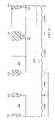
- FIG. 6illustrated is a cross sectional view of an embodiment of a partially completed semiconductor device including gates 240 for the PMOS, NMOS, P-LDMOS and N-LDMOS devices constructed in accordance with one or more aspects of the present invention.
- the process of forming the gates 240is preceded by forming gate dielectric layer 235 over the epitaxial layer 216 of the substrate 215 of a thickness consistent with the intended operating voltage of the gates 240 .
- the dielectric materialis typically silicon dioxide with a thickness of about five nanometers for devices employing about 0.25 micrometer feature sizes and operating at low gate voltages (e.g., 2.5 volts).
- a polysilicon layeris deposited over a surface of the gate dielectric layer 235 and doped N-type or P-type, using an appropriate doping specie.
- the polysilicon layeris annealed at an elevated temperature to properly diffuse the dopant.
- a photoresist maskis employed with an etch to define the lateral dimensions to define the gates 240 .
- the steps of depositing the dielectric and polysilicon layers, doping, annealing, and patterningare well known in the art and will not hereinafter be described in further detail.
- the gates 240may include a wide range of materials including various metals, doped semiconductors, or other conductive materials. Additionally, the gates 240 may have a wide range of thicknesses. The thickness of the gates 240 may range from about 100 to about 500 nanometers, but may be even smaller or larger depending on the application.
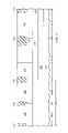
- FIG. 7illustrated is a cross sectional view of an embodiment of a partially completed semiconductor device including a lightly doped region (e.g., a N-type lightly doped region) 245 of a drain (also referred to as a “N-type lightly doped drain region”) for the N-LDMOS device constructed in accordance with one or more aspects of the present invention.
- the N-type lightly doped drain region 245allows the N-LDMOS device to accommodate higher voltage operation from the drain to the source thereof.
- the N-type lightly doped drain region 245may be formed employing an ion implantation process in connection with a photoresist mask to define the lateral dimensions thereof. Additionally, an annealing process at elevated temperatures distributes the implanted ion specie.
- FIG. 8illustrated is a cross sectional view of an embodiment of a partially completed semiconductor device including a lightly doped region (e.g., a P-type lightly doped region) 250 of a drain (also referred to as a “P-type lightly doped drain region”) for the P-LDMOS device constructed in accordance with one or more aspects of the present invention.
- the P-type lightly doped drain region 250allows the P-LDMOS device to accommodate higher voltage operation from the drain to the source thereof.
- the P-type lightly doped drain region 250may be formed employing an ion implantation process in connection with a photoresist mask to define the lateral dimensions thereof. Additionally, an annealing process at elevated temperatures distributes the implanted ion specie.
- the P-type lightly doped drain region 250is preferably doped, without limitation, to about 1 ⁇ 10 16 to 1 ⁇ 10 17 atoms/cm 3 .
- the steps of patterning, ion implanting and annealingare well known in the art and will not hereinafter be described in further detail.
- the N-type and P-type lightly doped drain regions 245 , 250provide higher voltage drains for the N-LDMOS and P-LDMOS devices, respectively.
- the N-type and P-type lightly doped drain regions 245 , 250form parasitic diodes with adjoining oppositely doped regions, namely, the P-type well 230 and N-type well 225 , respectively.
- the breakdown voltage of the parasitic diodesis determined by the doping concentration profiles, with lighter doping concentration profiles providing a higher breakdown voltage because the resulting internal electric fields are distributed over longer distances when the diodes are back biased. It is recognized that the width of the N-type and P-type lightly doped drain regions 245 , 250 may be individually varied to alter the breakdown voltage characteristics of the respective N-LDMOS and P-LDMOS devices without departing from the scope of the present invention.
- the N-type heavily doped regions 260 for the NMOS deviceare formed within the P-type well 230 thereof and, as alluded to above, form the source and the drain for the NMOS device. Additionally, the N-type heavily doped regions 262 for the N-LDMOS device are formed within the P-type well 230 thereof and, as alluded to above, form the source and a portion of the drain for the N-LDMOS device. Also, the N-type heavily doped region 262 of the drain for the N-LDMOS device is adjacent the N-type lightly doped drain region 245 thereof.
- the N-type heavily doped regions 260 , 262may be advantageously formed with an ion implantation process using dopant specie such as arsenic or phosphorus.
- the doping processincludes a photoresist mask to define lateral dimensions of the N-type heavily doped regions 260 , 262 and an annealing process at elevated temperature to properly distribute the implanted species.
- the N-type heavily doped region 260 for the source and drain of the NMOS deviceis doped, without limitation, to be greater than about 1 ⁇ 10 19 atoms/cm 3 .
- the N-type heavily doped region 262 for the source and drain of the N-LDMOS deviceis doped, without limitation, to be greater than about 5 ⁇ 10 19 atoms/cm 3 .
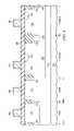
- FIG. 11illustrated is a cross sectional view of an embodiment of a partially completed semiconductor device including heavily doped regions for the source and drain for the PMOS and P-LDMOS devices constructed in accordance with one or more aspects of the present invention.
- the heavily doped regions (e.g., P-type heavily doped regions) 265 for the source and drain of the PMOS devicepreferably have a different doping concentration profile than the heavily doped regions (e.g., P-type heavily doped regions) 267 for the source and drain of the P-LDMOS device.
- the P-type heavily doped regions 265 for the PMOS deviceare formed within the N-type well 225 thereof and, as alluded to above, form the source and the drain for the PMOS device.
- the P-type heavily doped regions 267 for the P-LDMOS deviceare formed within the N-type well 225 or in a region adjacent the N-type well 225 thereof and, as alluded to above, form the source and a portion of the drain for the P-LDMOS device. Also, the P-type heavily doped region 267 of the drain for the P-LDMOS device is adjacent the P-type lightly doped drain region 250 thereof.
- the P-type heavily doped regions 265 , 267may be advantageously formed with an ion implantation process using dopant specie such as boron.
- the doping processincludes a photoresist mask to define lateral dimensions of the P-type heavily doped regions 265 , 267 and an annealing process at elevated temperature to properly distribute the implanted species.
- the P-type heavily doped region 265 for the source and drain of the PMOS deviceis doped, without limitation, to be greater than about 1 ⁇ 10 19 atoms/cm 3 .
- the P-type heavily doped region 267 for the source and drain of the P-LDMOS deviceis doped, without limitation, to be greater than about 5 ⁇ 10 19 atoms/cm 3 .
- the N-type well 225 above the N-type buried layer 220does not cover the entire area that accommodates the P-LDMOS device in the epitaxial layer 216 of the substrate 215 between the shallow trench isolation regions 210 thereof.
- the N-type well 225covers about half of the area that accommodates the P-LDMOS device through a channel region 270 that is adjacent to and extends between the P-type heavily doped region 267 of source and the P-type lightly doped drain region 250 of the drain, and under the gate 240 thereof recessed into the substrate 215 (or the overlying epitaxial layer 216 ).
- the N-type well 225is located under and within the channel region 270 , and the N-type well 225 and N-type buried layer 220 are oppositely doped in comparison to the P-type lightly and heavily doped regions 250 , 267 .
- the channel region 270is generally defined and well understood to be a conductive region between the source and drain (or the lightly or heavily doped regions thereof) of a transistor that is induced under the gate by a charge thereon.
- a doped region(e.g., a P-type doped region) 272 extends between the P-type heavily doped region 267 and the N-type well 225 of the P-LDMOS device and has a doping concentration profile less than a doping concentration profile of the P-type heavily doped region 267 .
- the P-type doped region 272happens to be embodied in the epitaxial layer 216 which has a doping concentration profile between 1 ⁇ 10 14 and 1 ⁇ 10 16 atoms/cm 3 .
- Employing the epitaxial layer 216 as the P-type doped region 272provides an opportunity to omit a masking and a processing step in the manufacture of the semiconductor device.
- the epitaxial layer 216may be omitted and the P-type doped region 272 may be formed in the substrate 215 (in this case, a P-type doped substrate).
- the P-type doped region 272may be formed by an ion implantation process prior to implanting the P-type heavily doped region 267 for the drain of the P-LDMOS device.
- the P-type doping materialsuch as boron would be implanted to provide a doping concentration profile less than a doping concentration profile of the P-type heavily doped region 267 .
- the P-type doped region 272may be formed with any doping concentration profile less than the P-type heavily doped region 267 including a doping concentration profile less than the P-type lightly doped drain region 250 and still be within the broad scope of the present invention.
- Incorporating the P-type doped region 272 into the P-LDMOS deviceincreases a breakdown voltage between the P-type heavily doped region 267 and the N-type well 225 of the P-LDMOS device. More specifically, in effect the P-type doped region 272 forms a parasitic diode with the adjoining oppositely doped N-type well 225 .
- the breakdown voltage of the parasitic diodeis determined by the doping concentration profiles, with lighter doping concentration profiles providing a higher breakdown voltage because the resulting internal electric fields are distributed over longer distances when the diodes are back biased.
- the P-LDMOS deviceexhibits a higher drain-to-source voltage handing capability due to the higher breakdown voltage thereof.
- the P-LDMOS devicecan handle voltages, without limitation, of ten volts while constructed on the same substrate 215 as the CMOS devices, namely, the PMOS and NMOS devices that operate at lower voltages (e.g., 2.5 volts). It should be understood that while the doped region has been described with respect to the P-LDMOS device, the principles are equally applicable to the N-LDMOS device and, for that matter, other transistors of analogous construction.
- FIG. 12illustrated is a cross sectional view of an embodiment of a partially completed semiconductor device including a salicide layer (one of which is designated 275 ) on the gate, source and drain of the NMOS, PMOS, N-LDMOS and P-LDMOS devices constructed in accordance with one or more aspects of the present invention.
- a salicide layerone of which is designated 275
- the formation of the salicide layer 275refers to deposition of a metal over silicon by a sputtering or other deposition process followed by an annealing process to improve a conductivity of polysilicon or other material and to facilitate the formation of ohmic contacts.
- a region for salicidationis exposed using a photoresist mask to selectively etch the gate dielectric 235 from the source and drain of the NMOS, PMOS. N-LDMOS and P-LDMOS devices.
- a metalgenerally titanium, is deposited and the substrate 215 is annealed at an elevated temperature. During the annealing process, metal in contact with silicon reacts with silicon to form the salicide layer 275 . The metal not in contact with silicon remains as metal, which can be etched away, leaving behind the salicide layer 275 .
- the steps of masking, depositing metal, annealing and etchingare well known in the art and will not hereinafter be described in further detail.
- FIG. 13illustrated is a cross sectional view of an embodiment of a partially completed semiconductor device including dielectric regions 280 for defining metal contacts constructed in accordance with one or more aspects of the present invention.
- the semiconductor deviceis illustrated following a masking, deposition and etching of a dielectric layer to define the dielectric regions 280 .
- the dielectric regions 280may be formed from an oxide or other suitable dielectric material.
- the dielectric regions 280are generally formed by blanket depositing the dielectric layer over the surface of the partially completed semiconductor device and anisotropically etching the dielectric layer, resulting in the dielectric regions 280 .
- the steps of depositing the dielectric layer, masking and etchingare well known in the art and will not hereinafter be described in further detail.
- FIG. 14illustrated is a cross sectional view of the semiconductor device including metal (ohmic) contacts 285 formed over the salicide layer 275 on the gate, source and drain of the NMOS, PMOS, N-LDMOS and P-LDMOS devices constructed in accordance with one or more aspects of the present invention.
- the embodimentillustrates the semiconductor device following deposition and patterning of a metal (e.g., aluminum) for the metal contacts 285 .
- the masking, etching, and further deposition of the dielectric and metal layersmay be repeated several times to provide multiple, highly conductive layers and interconnections in accordance with the parameters of the application.
- a four level metal interconnection arrangementmay be provided by incorporating several steps to form the multi-level metal contacts 285 .
- the metal contacts 285are formed about and defined by the dielectric layers 280 .
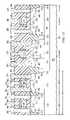
- the semiconductor deviceincludes shallow trench isolation regions 310 within a substrate 315 (e.g., P-type substrate) to provide dielectric separation between PMOS, NMOS, P-LDMOS and N-LDMOS devices.
- a buried layer (e.g., a N-type buried layer) 320is recessed within the substrate 315 in the area that accommodates the P-LDMOS device and the N-LDMOS device.
- the semiconductor devicealso includes wells (e.g., N-type wells) 325 formed in the substrate 315 in the areas that accommodate the PMOS device and the P-LDMOS device, and under the shallow trench isolation regions 310 above the N-type buried layer 320 (for the P-LDMOS).
- the N-type wells 325are formed to provide electrical isolation for the PMOS device and the P-LDMOS device and operate cooperatively with the N-type buried layer 320 (in the case of the P-LDMOS device) and the shallow trench isolation regions 310 to provide the isolation.
- the N-type well 325 above the N-type buried layer 320does not cover the entire area that accommodates the P-LDMOS device in the substrate 315 between the shallow trench isolation regions 310 thereof.
- the N-type well 325 for the P-LDMOSis constructed as such for the reasons as set forth herein.
- the semiconductor deviceincludes additional wells (e.g., P-type wells) 330 formed in the substrate 315 between the shallow trench isolation regions 310 substantially in the areas that accommodate the NMOS device and N-LDMOS device. While the P-type well 330 above the N-type buried layer 320 covers the entire area that accommodates the N-LDMOS device in the substrate 315 between the shallow trench isolation regions 310 thereof, it is well within the broad scope of the present invention to define the P-type well 330 to cover a portion of the area that accommodates the N-LDMOS device in the substrate 315 .
- the semiconductor devicealso includes gates 340 for the PMOS, NMOS, P-LDMOS and N-LDMOS devices located over a gate dielectric layer 335 and including gate sidewall spacers 355 about the gates 340 thereof.
- the N-LDMOS deviceincludes lightly doped regions (e.g., N-type lightly doped regions) 345 for the source and the drain thereof.
- the P-LDMOS devicealso includes lightly doped regions (e.g., P-type lightly doped regions) 350 for the source and the drain thereof.
- the N-type and P-type lightly doped regions 345 , 350provide higher voltage sources and drains for the N-LDMOS and P-LDMOS devices, respectively.
- the N-LDMOS and P-LDMOS deviceshandle higher voltages from the drain-to-source thereof, but the devices can handle a higher voltage from a source-to-gate thereof when the source is more positive than the gate 340 .
- the width of the N-type and P-type lightly doped regions 345 , 350may be individually varied to alter the breakdown voltage characteristics of the respective N-LDMOS and P-LDMOS devices without departing from the scope of the present invention. Additionally, the N-type and P-type lightly doped regions may be formed in a manner similar to the respective N-LDMOS and P-LDMOS devices illustrated and described with respect to FIGS. 2 through 14 .
- the semiconductor devicealso includes heavily doped regions (e.g., N-type heavily doped regions) 360 for the source and drain of the NMOS device that preferably have a different doping concentration profile than heavily doped regions (e.g., N-type heavily doped regions) 362 for the source and drain of the N-LDMOS device.
- the N-type heavily doped regions 360 for the NMOS deviceare formed within the P-type well 330 thereof and, as alluded to above, form the source and the drain for the NMOS device.
- the N-type heavily doped regions 362 for the N-LDMOS deviceare formed within the P-type well 330 thereof and, as alluded to above, form a portion of the source and the drain for the N-LDMOS device.
- the N-type heavily doped regions 362 of the source and drain for the N-LDMOS deviceare adjacent the N-type lightly doped drain regions 345 thereof.
- the semiconductor devicealso includes heavily doped regions (e.g., P-type heavily doped regions) 365 for the source and drain of the PMOS device that preferably have a different doping concentration profile than heavily doped regions (e.g., P-type heavily doped regions) 367 for the source and drain of the P-LDMOS device.
- the P-type heavily doped regions 365 for the PMOS deviceare formed within the N-type well 325 thereof and, as alluded to above, form the source and the drain for the PMOS device.
- the P-type heavily doped regions 367 for the P-LDMOS deviceare formed within the N-type well 325 or in regions adjacent the N-type well 325 thereof and, as alluded to above, form a portion of the source and the drain for the P-LDMOS device. Also, the P-type heavily doped regions 367 of the source and drain for the P-LDMOS device are adjacent the P-type lightly doped drain regions 350 thereof.
- the N-type well 325 above the N-type buried layer 320does not cover the entire area that accommodates the P-LDMOS device in the substrate 315 between the shallow trench isolation regions 310 thereof.
- the N-type well 325is located under and within a channel region 370 , and the N-type well 325 and N-type buried layer 320 are oppositely doped in comparison to the P-type lightly and heavily doped regions 350 , 367 .
- doped regionse.g., a P-type doped regions; also generally referred to as a “doped region and another doped region” 372 , 374 extend between the P-type heavily doped regions 367 and the N-type well 325 of the P-LDMOS device and have a doping concentration profile less than a doping concentration profile of the P-type heavily doped regions 367 .
- the P-type heavily doped regions 367preferably have the same doping concentration profiles, it is well within the broad scope of the present invention that the P-type heavily doped region 367 for the source has a different doping concentration profile than the counterpart of the drain. The same principle applies to other like regions of the devices of the semiconductor device.
- the P-type doped regions 372 , 374happen to be embodied in the substrate 315 which has a doping concentration profile between 1 ⁇ 10 14 and 1 ⁇ 10 16 atoms/cm 3 .
- Employing the substrate 315 as the P-type doped regions 372 , 374provides an opportunity to omit a masking and a processing step in the manufacture of the semiconductor device.
- the P-type doped regions 372 , 374may be formed by an ion implantation process prior to implanting the P-type heavily doped regions 367 for the source and the drain of the P-LDMOS device.
- the P-type doped regions 372 , 374may be formed with any doping concentration profile less than the P-type heavily doped regions 367 .
- incorporación of the P-type doped regions 372 , 374 into the P-LDMOS devicefurther increases a breakdown voltage between the P-type heavily doped regions 367 and the N-type well 325 of the P-LDMOS device.
- the P-LDMOS devicetherefore, exhibits a higher drain-to-source voltage handing capability due to the higher breakdown voltage thereof and provides a higher source-to-gate voltage handling capability when the source is more positive than the gate 340 . It should be understood that while the doped regions have been described with respect to the P-LDMOS device, the principles are equally applicable to the N-LDMOS device and, for that matter, other transistors of analogous construction.
- the P-LDMOS and N-LDMOS devices illustrated and described with respect to FIGS. 2 through 14are referred to as asymmetrical devices
- the P-LDMOS and N-LDMOS devices illustrated and described with respect to FIG. 15are referred to as symmetrical devices.
- the symmetrical nature of the source and drain of the semiconductor device of FIG. 15provide for a symmetrical device.
- the semiconductor devicealso includes metal contacts 385 defined by dielectric regions 380 formed over salicide layers (one of which is designated 375 ) for the gate, source and drain of the PMOS, NMOS, P-LDMOS and N-LDMOS devices.
- the development of a semiconductor device as described hereinretains the fine line structures and accommodates an operation at higher voltages and with higher switching frequencies (e.g., five megahertz).
- the LDMOS deviceBy introducing a doped region(s) between the heavily doped region and oppositely doped well, the LDMOS device exhibits a high voltage handling capability from the drain to the source thereof.
- the higher voltage deviceis constructed employing a limited number of additional processing steps.
- the LDMOS devicemay exhibit a low level gate-to-source voltage limit (e.g., 2.5 volts) and at the same time handle drain-to-source voltages above the gate-to-source voltage limit thereof.
- the LDMOS devicemay exhibit a higher level source-to-gate voltage handling capability (e.g, five volts) when the source is more positive than the gate and at the same time handle drain-to-source voltages above the low level gate-to-source voltage limit thereof.
- the LDMOS devicecan switch the larger currents normally associated with a power train of a power converter by appropriately designing selected regions thereof as set forth above.
- a transistore.g., a LDMOS device
- a transistore.g., a LDMOS device
- related method of constructing the samewith readily attainable and quantifiable advantages has been introduced.
- a transistore.g., a LDMOS device
- semiconductor device and related methods of constructing the sameare submitted for illustrative purposes only.
- other embodiments capable of producing a higher voltage devicesuch as a LDMOS device that can accommodate higher voltages and is capable of being integrated with low voltage devices on a semiconductor substrate in an integrate circuit that may form a power converter or portions thereof are well within the broad scope of the present invention.
- the LDMOS device and semiconductor devicemay be incorporated into an integrated circuit that forms a power converter or the like.
- the semiconductor devicemay be incorporated into an integrated circuit that forms another system such as a power amplifier, motor controller, and a system to control an actuator in accordance with a stepper motor or other electromechanical device.
Landscapes
- Engineering & Computer Science (AREA)
- Physics & Mathematics (AREA)
- Condensed Matter Physics & Semiconductors (AREA)
- General Physics & Mathematics (AREA)
- Manufacturing & Machinery (AREA)
- Computer Hardware Design (AREA)
- Microelectronics & Electronic Packaging (AREA)
- Power Engineering (AREA)
- Metal-Oxide And Bipolar Metal-Oxide Semiconductor Integrated Circuits (AREA)
- Insulated Gate Type Field-Effect Transistor (AREA)
Abstract
Description
Claims (18)
Priority Applications (13)
| Application Number | Priority Date | Filing Date | Title |
|---|---|---|---|
| US10/767,684US7230302B2 (en) | 2004-01-29 | 2004-01-29 | Laterally diffused metal oxide semiconductor device and method of forming the same |
| US11/286,929US7244994B2 (en) | 2004-01-29 | 2005-11-23 | Laterally diffused metal oxide semiconductor device and method of forming the same |
| US11/805,233US7759184B2 (en) | 2004-01-29 | 2007-05-22 | Laterally diffused metal oxide semiconductor device and method of forming the same |
| US11/841,375US8716790B2 (en) | 2004-01-29 | 2007-08-20 | Laterally diffused metal oxide semiconductor device and method of forming the same |
| US12/550,027US8253196B2 (en) | 2004-01-29 | 2009-08-28 | Integrated circuit with a laterally diffused metal oxide semiconductor device and method of forming the same |
| US12/549,836US8253197B2 (en) | 2004-01-29 | 2009-08-28 | Integrated circuit with a laterally diffused metal oxide semiconductor device and method of forming the same |
| US12/549,892US8212315B2 (en) | 2004-01-29 | 2009-08-28 | Integrated circuit with a laterally diffused metal oxide semiconductor device and method of forming the same |
| US12/549,944US8212317B2 (en) | 2004-01-29 | 2009-08-28 | Integrated circuit with a laterally diffused metal oxide semiconductor device and method of forming the same |
| US12/549,923US8212316B2 (en) | 2004-01-29 | 2009-08-28 | Integrated circuit with a laterally diffused metal oxide semiconductor device and method of forming the same |
| US12/550,002US8253195B2 (en) | 2004-01-29 | 2009-08-28 | Integrated circuit with a laterally diffused metal oxide semiconductor device and method of forming the same |
| US13/586,722US8633540B2 (en) | 2004-01-29 | 2012-08-15 | Integrated circuit with a laterally diffused metal oxide semiconductor device and method of forming the same |
| US14/156,676US8987815B2 (en) | 2004-01-29 | 2014-01-16 | Integrated circuit with a laterally diffused metal oxide semiconductor device and method of forming the same |
| US14/252,889US9680008B2 (en) | 2004-01-29 | 2014-04-15 | Laterally diffused metal oxide semiconductor device and method of forming the same |
Applications Claiming Priority (1)
| Application Number | Priority Date | Filing Date | Title |
|---|---|---|---|
| US10/767,684US7230302B2 (en) | 2004-01-29 | 2004-01-29 | Laterally diffused metal oxide semiconductor device and method of forming the same |
Related Child Applications (2)
| Application Number | Title | Priority Date | Filing Date |
|---|---|---|---|
| US11/286,929ContinuationUS7244994B2 (en) | 2004-01-29 | 2005-11-23 | Laterally diffused metal oxide semiconductor device and method of forming the same |
| US11/805,233DivisionUS7759184B2 (en) | 2004-01-29 | 2007-05-22 | Laterally diffused metal oxide semiconductor device and method of forming the same |
Publications (2)
| Publication Number | Publication Date |
|---|---|
| US20050167756A1 US20050167756A1 (en) | 2005-08-04 |
| US7230302B2true US7230302B2 (en) | 2007-06-12 |
Family
ID=34807716
Family Applications (5)
| Application Number | Title | Priority Date | Filing Date |
|---|---|---|---|
| US10/767,684Expired - Fee RelatedUS7230302B2 (en) | 2004-01-29 | 2004-01-29 | Laterally diffused metal oxide semiconductor device and method of forming the same |
| US11/286,929Expired - Fee RelatedUS7244994B2 (en) | 2004-01-29 | 2005-11-23 | Laterally diffused metal oxide semiconductor device and method of forming the same |
| US11/805,233Expired - LifetimeUS7759184B2 (en) | 2004-01-29 | 2007-05-22 | Laterally diffused metal oxide semiconductor device and method of forming the same |
| US11/841,375Active2026-06-30US8716790B2 (en) | 2004-01-29 | 2007-08-20 | Laterally diffused metal oxide semiconductor device and method of forming the same |
| US14/252,889Expired - Fee RelatedUS9680008B2 (en) | 2004-01-29 | 2014-04-15 | Laterally diffused metal oxide semiconductor device and method of forming the same |
Family Applications After (4)
| Application Number | Title | Priority Date | Filing Date |
|---|---|---|---|
| US11/286,929Expired - Fee RelatedUS7244994B2 (en) | 2004-01-29 | 2005-11-23 | Laterally diffused metal oxide semiconductor device and method of forming the same |
| US11/805,233Expired - LifetimeUS7759184B2 (en) | 2004-01-29 | 2007-05-22 | Laterally diffused metal oxide semiconductor device and method of forming the same |
| US11/841,375Active2026-06-30US8716790B2 (en) | 2004-01-29 | 2007-08-20 | Laterally diffused metal oxide semiconductor device and method of forming the same |
| US14/252,889Expired - Fee RelatedUS9680008B2 (en) | 2004-01-29 | 2014-04-15 | Laterally diffused metal oxide semiconductor device and method of forming the same |
Country Status (1)
| Country | Link |
|---|---|
| US (5) | US7230302B2 (en) |
Cited By (64)
| Publication number | Priority date | Publication date | Assignee | Title |
|---|---|---|---|---|
| US20060038237A1 (en)* | 2004-08-23 | 2006-02-23 | Lotfi Ashraf W | Integrated circuit incorporating higher voltage devices and low voltage devices therein |
| US20060096087A1 (en)* | 2004-11-10 | 2006-05-11 | Lotfi Ashraf W | Method of manufacturing a power module |
| US20060096088A1 (en)* | 2004-11-10 | 2006-05-11 | Lotfi Ashraf W | Method of manufacturing an encapsulated package for a magnetic device |
| US20070074386A1 (en)* | 2005-10-05 | 2007-04-05 | Lotfi Ashraf W | Method of forming a power module with a magnetic device having a conductive clip |
| US20070075816A1 (en)* | 2005-10-05 | 2007-04-05 | Lotfi Ashraf W | Power module with a magnetic device having a conductive clip |
| US20070075817A1 (en)* | 2005-10-05 | 2007-04-05 | Lotfi Ashraf W | Magnetic device having a conductive clip |
| US20070075815A1 (en)* | 2005-10-05 | 2007-04-05 | Lotfi Ashraf W | Method of forming a magnetic device having a conductive clip |
| US20070210777A1 (en)* | 2006-03-06 | 2007-09-13 | Cervera Pedro A | Controller for a power converter and method of operating the same |
| US20070224752A1 (en)* | 2004-01-29 | 2007-09-27 | Lotfi Ashraf W | Laterally diffused metal oxide semiconductor device and method of forming the same |
| US20080018366A1 (en)* | 2006-07-20 | 2008-01-24 | Enpirion, Inc. | Driver for switch and a method of driving the same |
| US20080094114A1 (en)* | 2006-10-20 | 2008-04-24 | Mirmira Ramarao Dwarakanath | Controller including a sawtooth generator and method of operating the same |
| US20090068400A1 (en)* | 2007-09-10 | 2009-03-12 | Lotfi Ashraf W | Micromagnetic Device and Method of Forming the Same |
| US20090065361A1 (en)* | 2007-09-10 | 2009-03-12 | Liakopoulos Trifon M | Electrolyte and Method of Producing the Same |
| US20090065363A1 (en)* | 2007-09-10 | 2009-03-12 | Liakopoulos Trifon M | Electroplating Cell and Tool |
| US20090068762A1 (en)* | 2007-09-10 | 2009-03-12 | Ken Takahashi | Methods of Processing a Substrate and Forming a Micromagnetic Device |
| US20090066300A1 (en)* | 2007-09-10 | 2009-03-12 | Lotfi Ashraf W | Power Converter Employing a Micromagnetic Device |
| US20090068347A1 (en)* | 2007-09-10 | 2009-03-12 | Lotfi Ashraf W | Method of Forming a Micromagnetic Device |
| US20090068761A1 (en)* | 2007-09-10 | 2009-03-12 | Lotfi Ashraf W | Method of Forming a Micromagnetic Device |
| US20090066467A1 (en)* | 2007-09-10 | 2009-03-12 | Lotfi Ashraf W | Micromagnetic Device and Method of Forming the Same |
| US20090167267A1 (en)* | 2007-12-27 | 2009-07-02 | Mirmira Ramarao Dwarakanath | Power Converter with Monotonic Turn-On for Pre-Charged Output Capacitor |
| US20090221105A1 (en)* | 2008-02-28 | 2009-09-03 | Renesas Technology Corp. | Manufacturing method for semiconductor integrated circuit device |
| US20090261791A1 (en)* | 2008-04-16 | 2009-10-22 | Lopata Douglas D | Power Converter with Power Switch Operable in Controlled Current Mode |
| US20100044789A1 (en)* | 2004-01-29 | 2010-02-25 | Enpirion, Incorporated | Integrated Circuit with a Laterally Diffused Metal Oxide Semiconductor Device and Method of Forming the Same |
| US20100052050A1 (en)* | 2004-01-29 | 2010-03-04 | Enpirion, Incorporated | Integrated Circuit with a Laterally Diffused Metal Oxide Semiconductor Device and Method of Forming the Same |
| US20100052049A1 (en)* | 2004-01-29 | 2010-03-04 | Enpirion, Incorporated, A Delaware Corporation | Integrated Circuit with a Laterally Diffused Metal Oxide Semiconductor Device and Method of Forming the Same |
| US20100052051A1 (en)* | 2004-01-29 | 2010-03-04 | Enpirion, Incorporated, A Delaware Corporation | Integrated Circuit with a Laterally Diffused Metal Oxide Semiconductor Device and Method of Forming the Same |
| US20100052052A1 (en)* | 2004-01-29 | 2010-03-04 | Enpirion, Incorporated | Integrated Circuit with a Laterally Diffused Metal Oxide Semiconductor Device and Method of Forming the Same |
| US20100087036A1 (en)* | 2008-10-02 | 2010-04-08 | Lotfi Ashraf W | Module having a stacked passive element and method of forming the same |
| US20100084750A1 (en)* | 2008-10-02 | 2010-04-08 | Lotfi Ashraf W | Module having a stacked passive element and method of forming the same |
| US7710093B2 (en) | 2004-01-29 | 2010-05-04 | Enpirion, Inc. | Driver for a power converter and a method of driving a switch thereof |
| US20100212150A1 (en)* | 2008-10-02 | 2010-08-26 | Lotfi Ashraf W | Module Having a Stacked Magnetic Device and Semiconductor Device and Method of Forming the Same |
| US20100214746A1 (en)* | 2008-10-02 | 2010-08-26 | Lotfi Ashraf W | Module Having a Stacked Magnetic Device and Semiconductor Device and Method of Forming the Same |
| US20110049621A1 (en)* | 2004-01-29 | 2011-03-03 | Enpirion Incorporated, A Delaware Corporation | Integrated Circuit with a Laterally Diffused Metal Oxide Semiconductor Device and Method of Forming the Same |
| US20110095742A1 (en)* | 2008-04-16 | 2011-04-28 | Douglas Dean Lopata | Power Converter with Controller Operable in Selected Modes of Operation |
| US20110101933A1 (en)* | 2008-04-16 | 2011-05-05 | Douglas Dean Lopata | Power Converter with Controller Operable in Selected Modes of Operation |
| US20110101934A1 (en)* | 2008-04-16 | 2011-05-05 | Douglas Dean Lopata | Power Converter with Controller Operable in Selected Modes of Operation |
| US8018315B2 (en) | 2007-09-10 | 2011-09-13 | Enpirion, Inc. | Power converter employing a micromagnetic device |
| TWI387107B (en)* | 2009-01-12 | 2013-02-21 | Vanguard Int Semiconduct Corp | Semiconductor device and method for fabricating the same and lateral diffused metal-oxide-semiconductor transistor and method for fabricating the same |
| US8686698B2 (en) | 2008-04-16 | 2014-04-01 | Enpirion, Inc. | Power converter with controller operable in selected modes of operation |
| US8698463B2 (en) | 2008-12-29 | 2014-04-15 | Enpirion, Inc. | Power converter with a dynamically configurable controller based on a power conversion mode |
| EP2738807A2 (en) | 2012-11-30 | 2014-06-04 | Enpirion, Inc. | An apparatus including a semiconductor device coupled to a decoupling device |
| US8867295B2 (en) | 2010-12-17 | 2014-10-21 | Enpirion, Inc. | Power converter for a memory module |
| US9246390B2 (en) | 2008-04-16 | 2016-01-26 | Enpirion, Inc. | Power converter with controller operable in selected modes of operation |
| US9509217B2 (en) | 2015-04-20 | 2016-11-29 | Altera Corporation | Asymmetric power flow controller for a power converter and method of operating the same |
| US9536938B1 (en) | 2013-11-27 | 2017-01-03 | Altera Corporation | Semiconductor device including a resistor metallic layer and method of forming the same |
| US9548714B2 (en) | 2008-12-29 | 2017-01-17 | Altera Corporation | Power converter with a dynamically configurable controller and output filter |
| US9673192B1 (en) | 2013-11-27 | 2017-06-06 | Altera Corporation | Semiconductor device including a resistor metallic layer and method of forming the same |
| US9673135B2 (en) | 2014-01-13 | 2017-06-06 | Altera Corporation | Semiconductor device having mirror-symmetric terminals and methods of forming the same |
| US9979294B1 (en)* | 2017-03-30 | 2018-05-22 | Semiconductor Components Industries, Llc | DC-DC converter with gate charge re-use |
| US10020739B2 (en) | 2014-03-27 | 2018-07-10 | Altera Corporation | Integrated current replicator and method of operating the same |
| US10103627B2 (en) | 2015-02-26 | 2018-10-16 | Altera Corporation | Packaged integrated circuit including a switch-mode regulator and method of forming the same |
| US10319854B1 (en) | 2017-12-05 | 2019-06-11 | Psemi Corporation | High voltage switching device |
| US10601300B2 (en) | 2017-05-19 | 2020-03-24 | Efficient Power Conversion Corporation | Integrated gallium nitride based DC-DC converter |
| US10903340B2 (en) | 2018-05-25 | 2021-01-26 | Silergy Semiconductor Technology (Hangzhou) Ltd | Laterally diffused metal oxide semiconductor structure and method for manufacturing the same |
| US10998305B2 (en) | 2018-08-20 | 2021-05-04 | Silergy Semiconductor Technology (Hangzhou) Ltd | Semiconductor die |
| US10998416B2 (en) | 2018-05-25 | 2021-05-04 | Silergy Semiconductor Technology (Hangzhou) Ltd | Laterally diffused metal oxide semiconductor device and method for manufacturing the same |
| US11031497B2 (en) | 2018-05-30 | 2021-06-08 | Silergy Semiconductor Technology (Hangzhou) Ltd | Semiconductor device and method for manufacturing the same |
| US11031388B2 (en) | 2018-08-17 | 2021-06-08 | Silergy Semiconductor Technology (Hangzhou) Ltd | Semiconductor structure and driving chip |
| US11121251B2 (en)* | 2018-05-25 | 2021-09-14 | Silergy Semiconductor Technology (Hangzhou) Ltd | Laterally diffused metal oxide semiconductor device and method for manufacturing the same |
| US11251276B2 (en) | 2018-05-29 | 2022-02-15 | Silergy Semiconductor Technology (Hangzhou) Ltd | LDMOS transistor and method for manufacturing the same |
| US11417647B2 (en) | 2018-08-17 | 2022-08-16 | Silergy Semiconductor Technology (Hangzhou) Ltd | Semiconductor structure having a semiconducture substrate and an isolation component |
| US11887889B2 (en) | 2020-06-08 | 2024-01-30 | Silergy Semiconductor Technology (Hangzhou) Ltd | Semiconductor device and method for manufacturing the same |
| US11949010B2 (en) | 2020-09-29 | 2024-04-02 | Silergy Semiconductor Technology (Hangzhou) Ltd | Metal oxide semiconductor device and method for manufacturing the same |
| WO2024257833A1 (en) | 2023-06-15 | 2024-12-19 | Murata Manufacturing Co., Ltd. | High-performance lateral mos transistor structures |
Families Citing this family (25)
| Publication number | Priority date | Publication date | Assignee | Title |
|---|---|---|---|---|
| JP2005142321A (en)* | 2003-11-06 | 2005-06-02 | Nec Electronics Corp | Semiconductor integrated circuit device and manufacturing method thereof |
| US7195981B2 (en)* | 2004-08-23 | 2007-03-27 | Enpirion, Inc. | Method of forming an integrated circuit employable with a power converter |
| US7190026B2 (en)* | 2004-08-23 | 2007-03-13 | Enpirion, Inc. | Integrated circuit employable with a power converter |
| US7232733B2 (en) | 2004-08-23 | 2007-06-19 | Enpirion, Inc. | Method of forming an integrated circuit incorporating higher voltage devices and low voltage devices therein |
| US7186606B2 (en)* | 2004-08-23 | 2007-03-06 | Enpirion, Inc. | Method of forming an integrated circuit employable with a power converter |
| US7015544B2 (en)* | 2004-08-23 | 2006-03-21 | Enpirion, Inc. | Intergrated circuit employable with a power converter |
| US7229886B2 (en)* | 2004-08-23 | 2007-06-12 | Enpirion, Inc. | Method of forming an integrated circuit incorporating higher voltage devices and low voltage devices therein |
| JP4513497B2 (en)* | 2004-10-19 | 2010-07-28 | ソニー株式会社 | Solid-state imaging device |
| US7864546B2 (en)* | 2007-02-13 | 2011-01-04 | Akros Silicon Inc. | DC-DC converter with communication across an isolation pathway |
| US7923710B2 (en) | 2007-03-08 | 2011-04-12 | Akros Silicon Inc. | Digital isolator with communication across an isolation barrier |
| US7701731B2 (en) | 2007-02-13 | 2010-04-20 | Akros Silicon Inc. | Signal communication across an isolation barrier |
| US20080136384A1 (en)* | 2006-12-06 | 2008-06-12 | Texas Instruments, Incorporated | Capacitor-free linear voltage regulator for integrated controller area network transceivers |
| US20080181316A1 (en)* | 2007-01-25 | 2008-07-31 | Philip John Crawley | Partitioned Signal and Power Transfer Across an Isolation Barrier |
| KR101398634B1 (en)* | 2008-07-11 | 2014-05-22 | 삼성전자주식회사 | Interconnection structure and electronic device employing the same |
| US20100054001A1 (en)* | 2008-08-26 | 2010-03-04 | Kenneth Dyer | AC/DC Converter with Power Factor Correction |
| JP5705610B2 (en)* | 2010-08-05 | 2015-04-22 | ルネサスエレクトロニクス株式会社 | Semiconductor device |
| US20150048875A1 (en)* | 2013-08-19 | 2015-02-19 | Ememory Technology Inc. | High voltage power control system |
| CN104916575B (en)* | 2014-03-11 | 2018-03-16 | 中芯国际集成电路制造(上海)有限公司 | A kind of manufacture method of semiconductor devices |
| US9660074B2 (en)* | 2014-08-07 | 2017-05-23 | Texas Instruments Incorporated | Methods and apparatus for LDMOS devices with cascaded RESURF implants and double buffers |
| US9105712B1 (en)* | 2014-09-02 | 2015-08-11 | Tower Semiconductors Ltd. | Double RESURF LDMOS with separately patterned P+ and N+ buried layers formed by shared mask |
| US10134641B2 (en)* | 2015-05-21 | 2018-11-20 | CoolStar Technology, Inc. | Enhanced integration of DMOS and CMOS semiconductor devices |
| US9673103B2 (en)* | 2015-06-30 | 2017-06-06 | Stmicroelectronics, Inc. | MOSFET devices with asymmetric structural configurations introducing different electrical characteristics |
| CN112530805B (en)* | 2019-09-19 | 2022-04-05 | 无锡华润上华科技有限公司 | Lateral double-diffused metal oxide semiconductor device and fabrication method thereof, and electronic device |
| US20230207630A1 (en)* | 2020-05-29 | 2023-06-29 | Sony Semiconductor Solutions Corporation | Semiconductor device |
| US12439663B2 (en) | 2021-07-09 | 2025-10-07 | Taiwan Semiconductor Manufacturing Company, Ltd. | Integration of low and high voltage devices on substrate |
Citations (52)
| Publication number | Priority date | Publication date | Assignee | Title |
|---|---|---|---|---|
| US4918026A (en) | 1989-03-17 | 1990-04-17 | Delco Electronics Corporation | Process for forming vertical bipolar transistors and high voltage CMOS in a single integrated circuit chip |
| US4947192A (en) | 1988-03-07 | 1990-08-07 | Xerox Corporation | Monolithic silicon integrated circuit chip for a thermal ink jet printer |
| US5014098A (en) | 1990-02-26 | 1991-05-07 | Delco Electronic Corporation | CMOS integrated circuit with EEPROM and method of manufacture |
| US5029283A (en) | 1990-03-28 | 1991-07-02 | Ncr Corporation | Low current driver for gate array |
| US5047358A (en) | 1989-03-17 | 1991-09-10 | Delco Electronics Corporation | Process for forming high and low voltage CMOS transistors on a single integrated circuit chip |
| US5156989A (en) | 1988-11-08 | 1992-10-20 | Siliconix, Incorporated | Complementary, isolated DMOS IC technology |
| US5169794A (en) | 1991-03-22 | 1992-12-08 | National Semiconductor Corporation | Method of fabrication of pnp structure in a common substrate containing npn or MOS structures |
| US5264782A (en) | 1992-08-10 | 1993-11-23 | International Business Machines Corporation | Dropout recovery circuit |
| US5285369A (en) | 1992-09-01 | 1994-02-08 | Power Integrations, Inc. | Switched mode power supply integrated circuit with start-up self-biasing |
| US5321319A (en) | 1992-06-08 | 1994-06-14 | Advanced Micro Devices, Inc. | High speed CMOS bus driver circuit that provides minimum output signal oscillation |
| US5366916A (en) | 1993-02-04 | 1994-11-22 | Delco Electronics Corporation | Method of making a high voltage implanted channel device for VLSI and ULSI processes |
| US5469334A (en) | 1991-09-09 | 1995-11-21 | Power Integrations, Inc. | Plastic quad-packaged switched-mode integrated circuit with integrated transformer windings and mouldings for transformer core pieces |
| US5504450A (en) | 1993-12-08 | 1996-04-02 | At&T Corp. | High voltage components for EEPROM system |
| US5610421A (en) | 1993-12-15 | 1997-03-11 | Sgs-Thomson Microelectronics S.R.L. | Integrated circuit with EPROM cells |
| US5644266A (en) | 1995-11-13 | 1997-07-01 | Chen; Ming-Jer | Dynamic threshold voltage scheme for low voltage CMOS inverter |
| US5710054A (en)* | 1996-08-26 | 1998-01-20 | Advanced Micro Devices, Inc. | Method of forming a shallow junction by diffusion from a silicon-based spacer |
| US5859606A (en) | 1997-07-25 | 1999-01-12 | Linear Technology Corporation | Interpolation circuit for digital-to-analog converter |
| US5888861A (en) | 1997-06-06 | 1999-03-30 | Integrated Device Technology, Inc. | Method of manufacturing a BiCMOS integrated circuit fully integrated within a CMOS process flow |
| US5889315A (en) | 1994-08-18 | 1999-03-30 | National Semiconductor Corporation | Semiconductor structure having two levels of buried regions |
| US5982645A (en) | 1992-08-25 | 1999-11-09 | Square D Company | Power conversion and distribution system |
| US6005377A (en) | 1997-09-17 | 1999-12-21 | Lucent Technologies Inc. | Programmable digital controller for switch mode power conversion and power supply employing the same |
| US6118351A (en) | 1997-06-10 | 2000-09-12 | Lucent Technologies Inc. | Micromagnetic device for power processing applications and method of manufacture therefor |
| US6204542B1 (en) | 1997-09-29 | 2001-03-20 | Kawasaki Steel Corporation | Field effect transistor with improved driving capability |
| US6255714B1 (en) | 1999-06-22 | 2001-07-03 | Agere Systems Guardian Corporation | Integrated circuit having a micromagnetic device including a ferromagnetic core and method of manufacture therefor |
| US6271063B1 (en) | 1997-06-24 | 2001-08-07 | Stmicroelectronics, Inc. | Method of making an SRAM cell and structure |
| US6288424B1 (en)* | 1998-09-23 | 2001-09-11 | U.S. Philips Corporation | Semiconductor device having LDMOS transistors and a screening layer |
| US6297108B1 (en) | 2000-03-10 | 2001-10-02 | United Microelectronics Corp. | Method of forming a high voltage MOS transistor on a semiconductor wafer |
| US6380004B2 (en) | 2000-02-02 | 2002-04-30 | International Rectifier Corp. | Process for manufacturing radhard power integrated circuit |
| US6384643B1 (en) | 1999-12-16 | 2002-05-07 | Texas Instruments Incorporated | Temperature and process compensated LDMOS drain-source voltage |
| US6384447B2 (en)* | 1999-12-17 | 2002-05-07 | Micron Technology, Inc. | Flash memory cell for high efficiency programming |
| US6392275B1 (en) | 1998-11-20 | 2002-05-21 | Fairchild Korea Semiconductor, Ltd. | Semiconductor device with DMOS, BJT and CMOS structures |
| US6413806B1 (en)* | 2000-02-23 | 2002-07-02 | Motorola, Inc. | Semiconductor device and method for protecting such device from a reversed drain voltage |
| US6420771B2 (en) | 1999-04-19 | 2002-07-16 | National Semiconductor Corporation | Trench isolated bipolar transistor structure integrated with CMOS technology |
| US6495019B1 (en) | 2000-04-19 | 2002-12-17 | Agere Systems Inc. | Device comprising micromagnetic components for power applications and process for forming device |
| US6521960B2 (en) | 1999-12-30 | 2003-02-18 | Hyundai Electronics Industries Co., Ltd. | Column transistor for semiconductor devices |
| US6541819B2 (en) | 2001-05-24 | 2003-04-01 | Agere Systems Inc. | Semiconductor device having non-power enhanced and power enhanced metal oxide semiconductor devices and a method of manufacture therefor |
| US6545360B1 (en) | 1999-09-07 | 2003-04-08 | Nec Corporation | Semiconductor device and manufacturing method thereof |
| US6551871B2 (en) | 2000-05-19 | 2003-04-22 | Sharp Kabushiki Kaisha | Process of manufacturing a dual gate CMOS transistor |
| US6653174B1 (en) | 1998-06-05 | 2003-11-25 | T-Ram, Inc. | Thyristor-based device over substrate surface |
| US20040094806A1 (en) | 2002-10-09 | 2004-05-20 | Antonino Schillaci | High performance, integrated, MOS-type semiconductor device and related manufacturing process |
| US6744676B2 (en) | 1998-08-14 | 2004-06-01 | Monolithic System Technology, Inc. | DRAM cell having a capacitor structure fabricated partially in a cavity and method for operating same |
| US6765272B2 (en) | 2001-04-27 | 2004-07-20 | Nec Electronics Corporation | Semiconductor device |
| US20040227190A1 (en)* | 2003-05-14 | 2004-11-18 | Jun Cai | ESD protection for semiconductor products |
| US6833585B2 (en) | 2001-04-16 | 2004-12-21 | Fairchild Korea Semiconductor | High voltage lateral DMOS transistor having low on-resistance and high breakdown voltage |
| US6855985B2 (en) | 2002-09-29 | 2005-02-15 | Advanced Analogic Technologies, Inc. | Modular bipolar-CMOS-DMOS analog integrated circuit & power transistor technology |
| US6900101B2 (en) | 2003-06-13 | 2005-05-31 | Texas Instruments Incorporated | LDMOS transistors and methods for making the same |
| US6911694B2 (en) | 2001-06-27 | 2005-06-28 | Ricoh Company, Ltd. | Semiconductor device and method for fabricating such device |
| US20050178084A1 (en) | 2003-03-27 | 2005-08-18 | Arno Haloila | Method and device for applying a plastic film around a product to be packaged |
| US20060040441A1 (en) | 2004-08-23 | 2006-02-23 | Lotfi Ashraf W | Method of forming an integrated circuit employable with a power converter |
| US20060040449A1 (en) | 2004-08-23 | 2006-02-23 | Lotfi Ashraf W | Method of forming an integrated circuit incorporating higher voltage devices and low voltage devices therein |
| US7012792B2 (en) | 2001-12-26 | 2006-03-14 | Nec Electronics Corporation | Semiconductor integrated circuit |
| US7015544B2 (en)* | 2004-08-23 | 2006-03-21 | Enpirion, Inc. | Intergrated circuit employable with a power converter |
Family Cites Families (137)
| Publication number | Priority date | Publication date | Assignee | Title |
|---|---|---|---|---|
| US4761725A (en) | 1986-08-01 | 1988-08-02 | Unisys Corporation | Digitally controlled A.C. to D.C. power conditioner |
| US5575743A (en)* | 1994-02-08 | 1996-11-19 | Medx Corporation | Method and apparatus for exercising adductor muscles |
| US4922327A (en) | 1987-12-24 | 1990-05-01 | University Of Toronto Innovations Foundation | Semiconductor LDMOS device with upper and lower passages |
| IT1235843B (en)* | 1989-06-14 | 1992-11-03 | Sgs Thomson Microelectronics | INTEGRATED DEVICE CONTAINING POWER STRUCTURES FORMED WITH COMPLEMENTARY LDMOS TRANSISTORS, CMOS AND PNP VERTICAL STRUCTURES WITH INCREASED CAPACITY TO SUPPORT A HIGH SUPPLY VOLTAGE. |
| US4982353A (en) | 1989-09-28 | 1991-01-01 | General Electric Company | Subsampling time-domain digital filter using sparsely clocked output latch |
| BE1003094A3 (en)* | 1990-11-19 | 1991-11-19 | Staar Sa | IMPROVEMENTS IN ORDERING AUDIO / VIDEO DEVICES FOR VEHICLES. |
| EP0487022B1 (en)* | 1990-11-23 | 1997-04-23 | Texas Instruments Incorporated | A method of simultaneously fabricating an insulated gate-field-effect transistor and a bipolar transistor |
| US5492847A (en)* | 1994-08-01 | 1996-02-20 | National Semiconductor Corporation | Counter-implantation method of manufacturing a semiconductor device with self-aligned anti-punchthrough pockets |
| US5405791A (en)* | 1994-10-04 | 1995-04-11 | Micron Semiconductor, Inc. | Process for fabricating ULSI CMOS circuits using a single polysilicon gate layer and disposable spacers |
| US6208535B1 (en) | 1994-10-31 | 2001-03-27 | Texas Instruments Incorporated | Resonant gate driver |
| US5469337A (en)* | 1994-11-14 | 1995-11-21 | General Electric Company | Multiple port high brightness centralized lighting system |
| DE69528961T2 (en)* | 1995-03-09 | 2003-09-04 | Stmicroelectronics S.R.L., Agrate Brianza | Method for manufacturing integrated circuits with high-voltage and low-voltage lateral DMOS power devices and non-volatile memory cells |
| US5594324A (en) | 1995-03-31 | 1997-01-14 | Space Systems/Loral, Inc. | Stabilized power converter having quantized duty cycle |
| JPH08335684A (en)* | 1995-06-08 | 1996-12-17 | Toshiba Corp | Semiconductor device |
| US5689213A (en) | 1995-08-23 | 1997-11-18 | Micron Technology, Inc. | Post-fabrication programmable integrated circuit ring oscillator |
| US5668024A (en)* | 1996-07-17 | 1997-09-16 | Taiwan Semiconductor Manufacturing Company | CMOS device structure with reduced risk of salicide bridging and reduced resistance via use of a ultra shallow, junction extension, ion implantation process |
| US5877611A (en) | 1996-10-09 | 1999-03-02 | Lucent Technologies Inc. | Simple and efficient switching regulator for fast transient loads such as microprocessors |
| US5899732A (en)* | 1997-04-11 | 1999-05-04 | Advanced Micro Devices, Inc. | Method of implanting silicon through a polysilicon gate for punchthrough control of a semiconductor device |
| KR100323554B1 (en) | 1997-05-14 | 2002-03-08 | 니시무로 타이죠 | Non-volatile semiconductor memory |
| US5930642A (en)* | 1997-06-09 | 1999-07-27 | Advanced Micro Devices, Inc. | Transistor with buried insulative layer beneath the channel region |
| US6236084B1 (en)* | 1998-06-01 | 2001-05-22 | Seiko Instruments Inc. | Semiconductor integrated circuit device having double diffusion insulated gate field effect transistor |
| JP2000048570A (en)* | 1998-07-28 | 2000-02-18 | Mitsubishi Electric Corp | Semiconductor storage device |
| US6333217B1 (en) | 1999-05-14 | 2001-12-25 | Matsushita Electric Industrial Co., Ltd. | Method of forming MOSFET with channel, extension and pocket implants |
| JP2001027909A (en) | 1999-07-13 | 2001-01-30 | Mitsubishi Electric Corp | Switch drive |
| JP3348782B2 (en)* | 1999-07-22 | 2002-11-20 | 日本電気株式会社 | Method for manufacturing semiconductor device |
| EP1094606B1 (en) | 1999-10-22 | 2004-03-03 | STMicroelectronics S.r.l. | Driver circuit for P-channel MOS switches |
| US6407579B1 (en) | 2000-01-20 | 2002-06-18 | Koninklijke Philips Electronics N.V. | Fast high voltage level shifter with gate oxide protection |
| US6365475B1 (en)* | 2000-03-27 | 2002-04-02 | United Microelectronics Corp. | Method of forming a MOS transistor |
| US6592019B2 (en) | 2000-04-27 | 2003-07-15 | Advanpack Solutions Pte. Ltd | Pillar connections for semiconductor chips and method of manufacture |
| US6578754B1 (en) | 2000-04-27 | 2003-06-17 | Advanpack Solutions Pte. Ltd. | Pillar connections for semiconductor chips and method of manufacture |
| US6388468B1 (en) | 2000-08-30 | 2002-05-14 | Yazaki North America | Circuit and method for operating a MOSFET control circuit with a system operating voltage greater than a maximum supply voltage limit |
| US6262564B1 (en) | 2000-11-10 | 2001-07-17 | Lucent Technologies Inc. | Driver for a controllable switch in a power converter |
| US6688985B2 (en) | 2001-02-07 | 2004-02-10 | Mattel, Inc. | Electrically controlled racing game with information and control center |
| US6489203B2 (en)* | 2001-05-07 | 2002-12-03 | Institute Of Microelectronics | Stacked LDD high frequency LDMOSFET |
| US6510976B2 (en) | 2001-05-18 | 2003-01-28 | Advanpack Solutions Pte. Ltd. | Method for forming a flip chip semiconductor package |
| JP4353393B2 (en) | 2001-06-05 | 2009-10-28 | 株式会社ルネサステクノロジ | Semiconductor integrated circuit device |
| US7109558B2 (en) | 2001-06-06 | 2006-09-19 | Denso Corporation | Power MOS transistor having capability for setting substrate potential independently of source potential |
| US6573694B2 (en) | 2001-06-27 | 2003-06-03 | Texas Instruments Incorporated | Stable low dropout, low impedance driver for linear regulators |
| US6550666B2 (en) | 2001-08-21 | 2003-04-22 | Advanpack Solutions Pte Ltd | Method for forming a flip chip on leadframe semiconductor package |
| TW548835B (en)* | 2001-08-30 | 2003-08-21 | Sony Corp | Semiconductor device and production method thereof |
| US6650169B2 (en) | 2001-10-01 | 2003-11-18 | Koninklijke Philips Electronics N.V. | Gate driver apparatus having an energy recovering circuit |
| US6730962B2 (en)* | 2001-12-07 | 2004-05-04 | Texas Instruments Incorporated | Method of manufacturing and structure of semiconductor device with field oxide structure |
| KR100418435B1 (en)* | 2001-12-26 | 2004-02-14 | 한국전자통신연구원 | Method for fabricating a power integrated circuit device |
| JP4098533B2 (en) | 2002-02-28 | 2008-06-11 | Tdk株式会社 | Control circuit for switching power supply device and switching power supply device using the same |
| US6777298B2 (en)* | 2002-06-14 | 2004-08-17 | International Business Machines Corporation | Elevated source drain disposable spacer CMOS |
| EP1376295B1 (en) | 2002-06-17 | 2008-08-13 | Hitachi, Ltd. | Power-supply device |
| US7719054B2 (en) | 2006-05-31 | 2010-05-18 | Advanced Analogic Technologies, Inc. | High-voltage lateral DMOS device |
| KR100489802B1 (en)* | 2002-12-18 | 2005-05-16 | 한국전자통신연구원 | Structure of high voltage device and low voltage device, and method of manufacturing the same |
| US7230316B2 (en) | 2002-12-27 | 2007-06-12 | Semiconductor Energy Laboratory Co., Ltd. | Semiconductor device having transferred integrated circuit |
| US6960512B2 (en)* | 2003-06-24 | 2005-11-01 | Taiwain Semiconductor Manufacturing Company, Ltd. | Method for manufacturing a semiconductor device having an improved disposable spacer |
| US6825531B1 (en)* | 2003-07-11 | 2004-11-30 | Micrel, Incorporated | Lateral DMOS transistor with a self-aligned drain region |
| US6822882B1 (en) | 2003-08-01 | 2004-11-23 | Tyco Electronics Power Systems, Inc. | Gate driver with a DC offset bias circuit and a power converter employing the same |
| US6924531B2 (en)* | 2003-10-01 | 2005-08-02 | Taiwan Semiconductor Manufacturing Company, Ltd. | LDMOS device with isolation guard rings |
| US6949961B2 (en)* | 2003-10-06 | 2005-09-27 | Semiconductor Components Industries, L.L.C. | Power switch structure with low RDSon and low current limit |
| KR100602110B1 (en)* | 2003-10-23 | 2006-07-19 | 동부일렉트로닉스 주식회사 | Semiconductor device having a double spacer and manufacturing method thereof |
| CA2448830C (en)* | 2003-11-06 | 2008-11-04 | D'anielo Rene Scotto | Multi-level litter tray for cats or other domestic animals |
| US7038274B2 (en)* | 2003-11-13 | 2006-05-02 | Volterra Semiconductor Corporation | Switching regulator with high-side p-type device |
| SE0303106D0 (en) | 2003-11-21 | 2003-11-21 | Infineon Technologies Ag | Ldmos transistor device, integrated circuit, and fabrication method thereof |
| SE0303099D0 (en) | 2003-11-21 | 2003-11-21 | Infineon Technologies Ag | Method in the fabrication of a monolithically integrated high frequency circuit |
| US7138698B2 (en) | 2003-12-18 | 2006-11-21 | Kabushiki Kaisha Toshiba | Semiconductor device including power MOS field-effect transistor and driver circuit driving thereof |
| US8212317B2 (en)* | 2004-01-29 | 2012-07-03 | Enpirion, Inc. | Integrated circuit with a laterally diffused metal oxide semiconductor device and method of forming the same |
| US7230302B2 (en)* | 2004-01-29 | 2007-06-12 | Enpirion, Inc. | Laterally diffused metal oxide semiconductor device and method of forming the same |
| US8253196B2 (en)* | 2004-01-29 | 2012-08-28 | Enpirion, Inc. | Integrated circuit with a laterally diffused metal oxide semiconductor device and method of forming the same |
| US7019505B2 (en) | 2004-01-29 | 2006-03-28 | Enpirion, Inc. | Digital controller for a power converter employing selectable phases of a clock signal |
| US8253195B2 (en)* | 2004-01-29 | 2012-08-28 | Enpirion, Inc. | Integrated circuit with a laterally diffused metal oxide semiconductor device and method of forming the same |
| US7330017B2 (en) | 2004-01-29 | 2008-02-12 | Enpirion, Inc. | Driver for a power converter and a method of driving a switch thereof |
| US8212315B2 (en)* | 2004-01-29 | 2012-07-03 | Enpirion, Inc. | Integrated circuit with a laterally diffused metal oxide semiconductor device and method of forming the same |
| US8212316B2 (en)* | 2004-01-29 | 2012-07-03 | Enpirion, Inc. | Integrated circuit with a laterally diffused metal oxide semiconductor device and method of forming the same |
| US7038438B2 (en) | 2004-01-29 | 2006-05-02 | Enpirion, Inc. | Controller for a power converter and a method of controlling a switch thereof |
| US8253197B2 (en) | 2004-01-29 | 2012-08-28 | Enpirion, Inc. | Integrated circuit with a laterally diffused metal oxide semiconductor device and method of forming the same |
| US7071044B1 (en) | 2004-05-05 | 2006-07-04 | Advanced Micro Devices, Inc. | Method of making a test structure for gate-body current and direct extraction of physical gate length using conventional CMOS |
| US7232762B2 (en)* | 2004-06-16 | 2007-06-19 | Taiwan Semiconductor Manufacturing Co., Ltd. | Method for forming an improved low power SRAM contact |
| US7422968B2 (en)* | 2004-07-29 | 2008-09-09 | Texas Instruments Incorporated | Method for manufacturing a semiconductor device having silicided regions |
| US7335948B2 (en) | 2004-08-23 | 2008-02-26 | Enpirion, Inc. | Integrated circuit incorporating higher voltage devices and low voltage devices therein |
| US7190026B2 (en) | 2004-08-23 | 2007-03-13 | Enpirion, Inc. | Integrated circuit employable with a power converter |
| US7195981B2 (en) | 2004-08-23 | 2007-03-27 | Enpirion, Inc. | Method of forming an integrated circuit employable with a power converter |
| US7214985B2 (en) | 2004-08-23 | 2007-05-08 | Enpirion, Inc. | Integrated circuit incorporating higher voltage devices and low voltage devices therein |
| US7229886B2 (en) | 2004-08-23 | 2007-06-12 | Enpirion, Inc. | Method of forming an integrated circuit incorporating higher voltage devices and low voltage devices therein |
| US7256674B2 (en)* | 2004-11-10 | 2007-08-14 | Enpirion, Inc. | Power module |
| US7426780B2 (en)* | 2004-11-10 | 2008-09-23 | Enpirion, Inc. | Method of manufacturing a power module |
| US7462317B2 (en)* | 2004-11-10 | 2008-12-09 | Enpirion, Inc. | Method of manufacturing an encapsulated package for a magnetic device |
| US7276998B2 (en)* | 2004-11-10 | 2007-10-02 | Enpirion, Inc. | Encapsulated package for a magnetic device |
| US7262476B2 (en) | 2004-11-30 | 2007-08-28 | Agere Systems Inc. | Semiconductor device having improved power density |
| US7365402B2 (en)* | 2005-01-06 | 2008-04-29 | Infineon Technologies Ag | LDMOS transistor |
| US7598606B2 (en) | 2005-02-22 | 2009-10-06 | Stats Chippac Ltd. | Integrated circuit package system with die and package combination |
| US7211516B2 (en)* | 2005-04-01 | 2007-05-01 | Texas Instruments Incorporated | Nickel silicide including indium and a method of manufacture therefor |
| US7344985B2 (en)* | 2005-04-01 | 2008-03-18 | Texas Instruments Incorporated | Nickel alloy silicide including indium and a method of manufacture therefor |
| US7422967B2 (en)* | 2005-05-12 | 2008-09-09 | Texas Instruments Incorporated | Method for manufacturing a semiconductor device containing metal silicide regions |
| KR100772097B1 (en) | 2005-06-11 | 2007-11-01 | 주식회사 하이닉스반도체 | Electrostatic Protection Devices for Semiconductor Circuits |
| US7420247B2 (en) | 2005-08-12 | 2008-09-02 | Cicion Semiconductor Device Corp. | Power LDMOS transistor |
| SG130099A1 (en) | 2005-08-12 | 2007-03-20 | Ciclon Semiconductor Device Co | Power ldmos transistor |
| US8278719B2 (en) | 2005-10-14 | 2012-10-02 | Silicon Space Technology Corp. | Radiation hardened isolation structures and fabrication methods |
| US8520402B1 (en) | 2005-10-25 | 2013-08-27 | Xilinx, Inc. | Decoupling capacitor circuit assembly |
| US7355217B1 (en) | 2005-11-22 | 2008-04-08 | National Semiconductor Corporation | MOS transistor structure with easy access to all nodes |
| US7521907B2 (en)* | 2006-03-06 | 2009-04-21 | Enpirion, Inc. | Controller for a power converter and method of operating the same |
| US7544558B2 (en)* | 2006-03-13 | 2009-06-09 | Bcd Semiconductor Manufacturing Limited | Method for integrating DMOS into sub-micron CMOS process |
| US20080001233A1 (en) | 2006-05-11 | 2008-01-03 | Ashok Kumar Kapoor | Semiconductor device with circuits formed with essentially uniform pattern density |
| US7364957B2 (en)* | 2006-07-20 | 2008-04-29 | Taiwan Semiconductor Manufacturing Company, Ltd. | Method and apparatus for semiconductor device with improved source/drain junctions |
| US20080142899A1 (en) | 2006-08-04 | 2008-06-19 | Silicon Space Technology Corporation | Radiation immunity of integrated circuits using backside die contact and electrically conductive layers |
| TWI370515B (en) | 2006-09-29 | 2012-08-11 | Megica Corp | Circuit component |
| US7408211B2 (en) | 2006-11-10 | 2008-08-05 | United Microelectronics Corp. | Transfer transistor of CMOS image sensor |
| US7892931B2 (en) | 2006-12-20 | 2011-02-22 | Texas Instruments Incorporated | Use of a single mask during the formation of a transistor's drain extension and recessed strained epi regions |
| FR2911005B1 (en) | 2006-12-27 | 2009-06-12 | St Microelectronics Sa | TRANSISTOR MOS ADAPTED TO KEEP STRONG FORTS |
| US8835263B2 (en) | 2007-02-21 | 2014-09-16 | Texas Instruments Incorporated | Formation of a selective carbon-doped epitaxial cap layer on selective epitaxial SiGe |
| GB2447509A (en) | 2007-03-16 | 2008-09-17 | Seiko Epson Corp | Pattern for Inkjet TFT circuit development |
| US8030731B2 (en) | 2007-03-28 | 2011-10-04 | Advanced Analogic Technologies, Inc. | Isolated rectifier diode |
| US7737526B2 (en) | 2007-03-28 | 2010-06-15 | Advanced Analogic Technologies, Inc. | Isolated trench MOSFET in epi-less semiconductor sustrate |
| US20080242032A1 (en) | 2007-03-29 | 2008-10-02 | Texas Instruments Incorporated | Carbon-Doped Epitaxial SiGe |
| US7626233B2 (en) | 2007-04-23 | 2009-12-01 | Infineon Technologies Ag | LDMOS device |
| US7544995B2 (en)* | 2007-09-10 | 2009-06-09 | Enpirion, Inc. | Power converter employing a micromagnetic device |
| US7952459B2 (en) | 2007-09-10 | 2011-05-31 | Enpirion, Inc. | Micromagnetic device and method of forming the same |
| US7808222B2 (en) | 2007-10-12 | 2010-10-05 | Monolithic Power Systems, Inc. | Method and apparatus for high performance switch mode voltage regulators |
| US7882482B2 (en) | 2007-10-12 | 2011-02-01 | Monolithic Power Systems, Inc. | Layout schemes and apparatus for high performance DC-DC output stage |
| US7876080B2 (en)* | 2007-12-27 | 2011-01-25 | Enpirion, Inc. | Power converter with monotonic turn-on for pre-charged output capacitor |
| US8410769B2 (en) | 2008-04-16 | 2013-04-02 | Enpirion, Inc. | Power converter with controller operable in selected modes of operation |
| US8541991B2 (en) | 2008-04-16 | 2013-09-24 | Enpirion, Inc. | Power converter with controller operable in selected modes of operation |
| US8686698B2 (en) | 2008-04-16 | 2014-04-01 | Enpirion, Inc. | Power converter with controller operable in selected modes of operation |
| US8692532B2 (en) | 2008-04-16 | 2014-04-08 | Enpirion, Inc. | Power converter with controller operable in selected modes of operation |
| US7679342B2 (en) | 2008-04-16 | 2010-03-16 | Enpirion, Inc. | Power converter with power switch operable in controlled current mode |
| US9246390B2 (en) | 2008-04-16 | 2016-01-26 | Enpirion, Inc. | Power converter with controller operable in selected modes of operation |
| US20090296310A1 (en) | 2008-06-03 | 2009-12-03 | Azuma Chikara | Chip capacitor precursors, packaged semiconductors, and assembly method for converting the precursors to capacitors |
| US8102679B2 (en) | 2008-08-15 | 2012-01-24 | Infineon Technologies Ag | Utilization of a multifunctional pin to control a switched-mode power converter |
| US7710094B1 (en) | 2008-12-12 | 2010-05-04 | Hong Kong Applied Science And Technology Research Institute Co., Ltd. | Current-mode-controlled current sensor circuit for power switching converter |
| US9548714B2 (en) | 2008-12-29 | 2017-01-17 | Altera Corporation | Power converter with a dynamically configurable controller and output filter |
| US8698463B2 (en) | 2008-12-29 | 2014-04-15 | Enpirion, Inc. | Power converter with a dynamically configurable controller based on a power conversion mode |
| US20100244152A1 (en) | 2009-03-27 | 2010-09-30 | Bahl Sandeep R | Configuration and fabrication of semiconductor structure having extended-drain field-effect transistor |
| US8101479B2 (en)* | 2009-03-27 | 2012-01-24 | National Semiconductor Corporation | Fabrication of asymmetric field-effect transistors using L-shaped spacers |
| US8358014B2 (en) | 2009-05-28 | 2013-01-22 | Texas Instruments Incorporated | Structure and method for power field effect transistor |
| US20110006763A1 (en) | 2009-07-07 | 2011-01-13 | Anthonius Bakker | Hall effect current sensor system and associated flip-chip packaging |
| US8400784B2 (en) | 2009-08-10 | 2013-03-19 | Silergy Technology | Flip chip package for monolithic switching regulator |
| JP5423269B2 (en) | 2009-09-15 | 2014-02-19 | 富士通セミコンダクター株式会社 | Semiconductor device and manufacturing method thereof |
| US8273617B2 (en) | 2009-09-30 | 2012-09-25 | Suvolta, Inc. | Electronic devices and systems, and methods for making and using the same |
| EP2400552A1 (en) | 2010-06-24 | 2011-12-28 | Dialog Semiconductor GmbH | Mos transistor structure with easy access to all nodes |
| JP2012073131A (en) | 2010-09-29 | 2012-04-12 | Sanken Electric Co Ltd | Current detection circuit |
| US8868893B2 (en) | 2011-12-13 | 2014-10-21 | Active-Semi, Inc. | Multi-mode power manager for power management integrated circuit |
| US20140159130A1 (en) | 2012-11-30 | 2014-06-12 | Enpirion, Inc. | Apparatus including a semiconductor device coupled to a decoupling device |
| US10020739B2 (en) | 2014-03-27 | 2018-07-10 | Altera Corporation | Integrated current replicator and method of operating the same |
- 2004
- 2004-01-29USUS10/767,684patent/US7230302B2/ennot_activeExpired - Fee Related
- 2005
- 2005-11-23USUS11/286,929patent/US7244994B2/ennot_activeExpired - Fee Related
- 2007
- 2007-05-22USUS11/805,233patent/US7759184B2/ennot_activeExpired - Lifetime
- 2007-08-20USUS11/841,375patent/US8716790B2/enactiveActive
- 2014
- 2014-04-15USUS14/252,889patent/US9680008B2/ennot_activeExpired - Fee Related
Patent Citations (55)
| Publication number | Priority date | Publication date | Assignee | Title |
|---|---|---|---|---|
| US4947192A (en) | 1988-03-07 | 1990-08-07 | Xerox Corporation | Monolithic silicon integrated circuit chip for a thermal ink jet printer |
| US5156989A (en) | 1988-11-08 | 1992-10-20 | Siliconix, Incorporated | Complementary, isolated DMOS IC technology |
| US5485027A (en) | 1988-11-08 | 1996-01-16 | Siliconix Incorporated | Isolated DMOS IC technology |
| US5047358A (en) | 1989-03-17 | 1991-09-10 | Delco Electronics Corporation | Process for forming high and low voltage CMOS transistors on a single integrated circuit chip |
| US4918026A (en) | 1989-03-17 | 1990-04-17 | Delco Electronics Corporation | Process for forming vertical bipolar transistors and high voltage CMOS in a single integrated circuit chip |
| US5014098A (en) | 1990-02-26 | 1991-05-07 | Delco Electronic Corporation | CMOS integrated circuit with EEPROM and method of manufacture |
| US5029283A (en) | 1990-03-28 | 1991-07-02 | Ncr Corporation | Low current driver for gate array |
| US5029283B1 (en) | 1990-03-28 | 1993-04-06 | Ncr Co | |
| US5169794A (en) | 1991-03-22 | 1992-12-08 | National Semiconductor Corporation | Method of fabrication of pnp structure in a common substrate containing npn or MOS structures |
| US5469334A (en) | 1991-09-09 | 1995-11-21 | Power Integrations, Inc. | Plastic quad-packaged switched-mode integrated circuit with integrated transformer windings and mouldings for transformer core pieces |
| US5321319A (en) | 1992-06-08 | 1994-06-14 | Advanced Micro Devices, Inc. | High speed CMOS bus driver circuit that provides minimum output signal oscillation |
| US5264782A (en) | 1992-08-10 | 1993-11-23 | International Business Machines Corporation | Dropout recovery circuit |
| US5982645A (en) | 1992-08-25 | 1999-11-09 | Square D Company | Power conversion and distribution system |
| US5285369A (en) | 1992-09-01 | 1994-02-08 | Power Integrations, Inc. | Switched mode power supply integrated circuit with start-up self-biasing |
| US5366916A (en) | 1993-02-04 | 1994-11-22 | Delco Electronics Corporation | Method of making a high voltage implanted channel device for VLSI and ULSI processes |
| US5504450A (en) | 1993-12-08 | 1996-04-02 | At&T Corp. | High voltage components for EEPROM system |
| US5610421A (en) | 1993-12-15 | 1997-03-11 | Sgs-Thomson Microelectronics S.R.L. | Integrated circuit with EPROM cells |
| US5889315A (en) | 1994-08-18 | 1999-03-30 | National Semiconductor Corporation | Semiconductor structure having two levels of buried regions |
| US5644266A (en) | 1995-11-13 | 1997-07-01 | Chen; Ming-Jer | Dynamic threshold voltage scheme for low voltage CMOS inverter |
| US5710054A (en)* | 1996-08-26 | 1998-01-20 | Advanced Micro Devices, Inc. | Method of forming a shallow junction by diffusion from a silicon-based spacer |
| US5888861A (en) | 1997-06-06 | 1999-03-30 | Integrated Device Technology, Inc. | Method of manufacturing a BiCMOS integrated circuit fully integrated within a CMOS process flow |
| US6118351A (en) | 1997-06-10 | 2000-09-12 | Lucent Technologies Inc. | Micromagnetic device for power processing applications and method of manufacture therefor |
| US6271063B1 (en) | 1997-06-24 | 2001-08-07 | Stmicroelectronics, Inc. | Method of making an SRAM cell and structure |
| US5859606A (en) | 1997-07-25 | 1999-01-12 | Linear Technology Corporation | Interpolation circuit for digital-to-analog converter |
| US6005377A (en) | 1997-09-17 | 1999-12-21 | Lucent Technologies Inc. | Programmable digital controller for switch mode power conversion and power supply employing the same |
| US6204542B1 (en) | 1997-09-29 | 2001-03-20 | Kawasaki Steel Corporation | Field effect transistor with improved driving capability |
| US6653174B1 (en) | 1998-06-05 | 2003-11-25 | T-Ram, Inc. | Thyristor-based device over substrate surface |
| US6744676B2 (en) | 1998-08-14 | 2004-06-01 | Monolithic System Technology, Inc. | DRAM cell having a capacitor structure fabricated partially in a cavity and method for operating same |
| US6288424B1 (en)* | 1998-09-23 | 2001-09-11 | U.S. Philips Corporation | Semiconductor device having LDMOS transistors and a screening layer |
| US6392275B1 (en) | 1998-11-20 | 2002-05-21 | Fairchild Korea Semiconductor, Ltd. | Semiconductor device with DMOS, BJT and CMOS structures |
| US6420771B2 (en) | 1999-04-19 | 2002-07-16 | National Semiconductor Corporation | Trench isolated bipolar transistor structure integrated with CMOS technology |
| US6255714B1 (en) | 1999-06-22 | 2001-07-03 | Agere Systems Guardian Corporation | Integrated circuit having a micromagnetic device including a ferromagnetic core and method of manufacture therefor |
| US6545360B1 (en) | 1999-09-07 | 2003-04-08 | Nec Corporation | Semiconductor device and manufacturing method thereof |
| US6384643B1 (en) | 1999-12-16 | 2002-05-07 | Texas Instruments Incorporated | Temperature and process compensated LDMOS drain-source voltage |
| US6384447B2 (en)* | 1999-12-17 | 2002-05-07 | Micron Technology, Inc. | Flash memory cell for high efficiency programming |
| US6521960B2 (en) | 1999-12-30 | 2003-02-18 | Hyundai Electronics Industries Co., Ltd. | Column transistor for semiconductor devices |
| US6380004B2 (en) | 2000-02-02 | 2002-04-30 | International Rectifier Corp. | Process for manufacturing radhard power integrated circuit |
| US6413806B1 (en)* | 2000-02-23 | 2002-07-02 | Motorola, Inc. | Semiconductor device and method for protecting such device from a reversed drain voltage |
| US6297108B1 (en) | 2000-03-10 | 2001-10-02 | United Microelectronics Corp. | Method of forming a high voltage MOS transistor on a semiconductor wafer |
| US6495019B1 (en) | 2000-04-19 | 2002-12-17 | Agere Systems Inc. | Device comprising micromagnetic components for power applications and process for forming device |
| US6551871B2 (en) | 2000-05-19 | 2003-04-22 | Sharp Kabushiki Kaisha | Process of manufacturing a dual gate CMOS transistor |
| US6833585B2 (en) | 2001-04-16 | 2004-12-21 | Fairchild Korea Semiconductor | High voltage lateral DMOS transistor having low on-resistance and high breakdown voltage |
| US6765272B2 (en) | 2001-04-27 | 2004-07-20 | Nec Electronics Corporation | Semiconductor device |
| US6541819B2 (en) | 2001-05-24 | 2003-04-01 | Agere Systems Inc. | Semiconductor device having non-power enhanced and power enhanced metal oxide semiconductor devices and a method of manufacture therefor |
| US6911694B2 (en) | 2001-06-27 | 2005-06-28 | Ricoh Company, Ltd. | Semiconductor device and method for fabricating such device |
| US20060027864A1 (en) | 2001-06-27 | 2006-02-09 | Takaaki Negoro | Semiconductor device and method for fabricating such device |
| US7012792B2 (en) | 2001-12-26 | 2006-03-14 | Nec Electronics Corporation | Semiconductor integrated circuit |
| US6855985B2 (en) | 2002-09-29 | 2005-02-15 | Advanced Analogic Technologies, Inc. | Modular bipolar-CMOS-DMOS analog integrated circuit & power transistor technology |
| US20040094806A1 (en) | 2002-10-09 | 2004-05-20 | Antonino Schillaci | High performance, integrated, MOS-type semiconductor device and related manufacturing process |
| US20050178084A1 (en) | 2003-03-27 | 2005-08-18 | Arno Haloila | Method and device for applying a plastic film around a product to be packaged |
| US20040227190A1 (en)* | 2003-05-14 | 2004-11-18 | Jun Cai | ESD protection for semiconductor products |
| US6900101B2 (en) | 2003-06-13 | 2005-05-31 | Texas Instruments Incorporated | LDMOS transistors and methods for making the same |
| US20060040441A1 (en) | 2004-08-23 | 2006-02-23 | Lotfi Ashraf W | Method of forming an integrated circuit employable with a power converter |
| US20060040449A1 (en) | 2004-08-23 | 2006-02-23 | Lotfi Ashraf W | Method of forming an integrated circuit incorporating higher voltage devices and low voltage devices therein |
| US7015544B2 (en)* | 2004-08-23 | 2006-03-21 | Enpirion, Inc. | Intergrated circuit employable with a power converter |
Non-Patent Citations (4)
| Title |
|---|
| Betancourt-Zamora, R.J. et al., "A 1.5 mW, 200 MHz CMOS VCO for Wireless Biotelemetry," First International Workshop on Design of Mixed-Mode Integrated Circuits and Applications, Cancun, Mexico, pp. 72-74, Jul. 1997. |
| Goodman, J. et al., "An Energy/Security Encryption Processor Using an Embedded Variable Voltage DC/DC Converter," IEEE Journal of Solid-State Circuits, vol. 33, No. 11 (Nov. 1998). |
| Horowitz, P., et al., "The Art of Electronics," Second Edition, 1989, pp. 288-291, Cambridge University Press, Cambridge, MA. |
| Lotfi, A.W., et al., "Issues and Advances in High-Frequency Magnetics for Switching Power Supplies," Proceedings of the IEEE, Jun. 2001, vol. 89, No. 6, pp. 833-845. |
Cited By (141)
| Publication number | Priority date | Publication date | Assignee | Title |
|---|---|---|---|---|
| US8633540B2 (en) | 2004-01-29 | 2014-01-21 | Enpirion, Inc. | Integrated circuit with a laterally diffused metal oxide semiconductor device and method of forming the same |
| US8212316B2 (en)* | 2004-01-29 | 2012-07-03 | Enpirion, Inc. | Integrated circuit with a laterally diffused metal oxide semiconductor device and method of forming the same |
| US8987815B2 (en) | 2004-01-29 | 2015-03-24 | Enpirion, Inc. | Integrated circuit with a laterally diffused metal oxide semiconductor device and method of forming the same |
| US7759184B2 (en)* | 2004-01-29 | 2010-07-20 | Enpirion, Inc. | Laterally diffused metal oxide semiconductor device and method of forming the same |
| US7710093B2 (en) | 2004-01-29 | 2010-05-04 | Enpirion, Inc. | Driver for a power converter and a method of driving a switch thereof |
| US9680008B2 (en) | 2004-01-29 | 2017-06-13 | Empirion, Inc. | Laterally diffused metal oxide semiconductor device and method of forming the same |
| US8212317B2 (en)* | 2004-01-29 | 2012-07-03 | Enpirion, Inc. | Integrated circuit with a laterally diffused metal oxide semiconductor device and method of forming the same |
| US20100052052A1 (en)* | 2004-01-29 | 2010-03-04 | Enpirion, Incorporated | Integrated Circuit with a Laterally Diffused Metal Oxide Semiconductor Device and Method of Forming the Same |
| US20070224752A1 (en)* | 2004-01-29 | 2007-09-27 | Lotfi Ashraf W | Laterally diffused metal oxide semiconductor device and method of forming the same |
| US20100052051A1 (en)* | 2004-01-29 | 2010-03-04 | Enpirion, Incorporated, A Delaware Corporation | Integrated Circuit with a Laterally Diffused Metal Oxide Semiconductor Device and Method of Forming the Same |
| US20110049621A1 (en)* | 2004-01-29 | 2011-03-03 | Enpirion Incorporated, A Delaware Corporation | Integrated Circuit with a Laterally Diffused Metal Oxide Semiconductor Device and Method of Forming the Same |
| US20100052049A1 (en)* | 2004-01-29 | 2010-03-04 | Enpirion, Incorporated, A Delaware Corporation | Integrated Circuit with a Laterally Diffused Metal Oxide Semiconductor Device and Method of Forming the Same |
| US8253197B2 (en)* | 2004-01-29 | 2012-08-28 | Enpirion, Inc. | Integrated circuit with a laterally diffused metal oxide semiconductor device and method of forming the same |
| US20100052050A1 (en)* | 2004-01-29 | 2010-03-04 | Enpirion, Incorporated | Integrated Circuit with a Laterally Diffused Metal Oxide Semiconductor Device and Method of Forming the Same |
| US20100044789A1 (en)* | 2004-01-29 | 2010-02-25 | Enpirion, Incorporated | Integrated Circuit with a Laterally Diffused Metal Oxide Semiconductor Device and Method of Forming the Same |
| US8212315B2 (en)* | 2004-01-29 | 2012-07-03 | Enpirion, Inc. | Integrated circuit with a laterally diffused metal oxide semiconductor device and method of forming the same |
| US8716790B2 (en) | 2004-01-29 | 2014-05-06 | Enpirion, Inc. | Laterally diffused metal oxide semiconductor device and method of forming the same |
| US8253195B2 (en)* | 2004-01-29 | 2012-08-28 | Enpirion, Inc. | Integrated circuit with a laterally diffused metal oxide semiconductor device and method of forming the same |
| US8253196B2 (en)* | 2004-01-29 | 2012-08-28 | Enpirion, Inc. | Integrated circuit with a laterally diffused metal oxide semiconductor device and method of forming the same |
| US7335948B2 (en) | 2004-08-23 | 2008-02-26 | Enpirion, Inc. | Integrated circuit incorporating higher voltage devices and low voltage devices therein |
| US20060038237A1 (en)* | 2004-08-23 | 2006-02-23 | Lotfi Ashraf W | Integrated circuit incorporating higher voltage devices and low voltage devices therein |
| US7426780B2 (en) | 2004-11-10 | 2008-09-23 | Enpirion, Inc. | Method of manufacturing a power module |
| US7462317B2 (en) | 2004-11-10 | 2008-12-09 | Enpirion, Inc. | Method of manufacturing an encapsulated package for a magnetic device |
| US20060096087A1 (en)* | 2004-11-10 | 2006-05-11 | Lotfi Ashraf W | Method of manufacturing a power module |
| US20090065964A1 (en)* | 2004-11-10 | 2009-03-12 | Lotfi Ashraf W | Method of Manufacturing an Encapsulated Package for a Magnetic Device |
| US20060096088A1 (en)* | 2004-11-10 | 2006-05-11 | Lotfi Ashraf W | Method of manufacturing an encapsulated package for a magnetic device |
| US8528190B2 (en) | 2004-11-10 | 2013-09-10 | Enpirion, Inc. | Method of manufacturing a power module |
| US8043544B2 (en) | 2004-11-10 | 2011-10-25 | Enpirion, Inc. | Method of manufacturing an encapsulated package for a magnetic device |
| US20070075815A1 (en)* | 2005-10-05 | 2007-04-05 | Lotfi Ashraf W | Method of forming a magnetic device having a conductive clip |
| US8384506B2 (en) | 2005-10-05 | 2013-02-26 | Enpirion, Inc. | Magnetic device having a conductive clip |
| US10304615B2 (en) | 2005-10-05 | 2019-05-28 | Enpirion, Inc. | Method of forming a power module with a magnetic device having a conductive clip |
| US8701272B2 (en) | 2005-10-05 | 2014-04-22 | Enpirion, Inc. | Method of forming a power module with a magnetic device having a conductive clip |
| US8631560B2 (en) | 2005-10-05 | 2014-01-21 | Enpirion, Inc. | Method of forming a magnetic device having a conductive clip |
| US8139362B2 (en) | 2005-10-05 | 2012-03-20 | Enpirion, Inc. | Power module with a magnetic device having a conductive clip |
| US20070074386A1 (en)* | 2005-10-05 | 2007-04-05 | Lotfi Ashraf W | Method of forming a power module with a magnetic device having a conductive clip |
| US7688172B2 (en) | 2005-10-05 | 2010-03-30 | Enpirion, Inc. | Magnetic device having a conductive clip |
| US20100176905A1 (en)* | 2005-10-05 | 2010-07-15 | Lotfi Ashraf W | Magnetic Device Having a Conductive Clip |
| US20070075817A1 (en)* | 2005-10-05 | 2007-04-05 | Lotfi Ashraf W | Magnetic device having a conductive clip |
| US20070075816A1 (en)* | 2005-10-05 | 2007-04-05 | Lotfi Ashraf W | Power module with a magnetic device having a conductive clip |
| US8013580B2 (en) | 2006-03-06 | 2011-09-06 | Enpirion, Inc. | Controller for a power converter and method of operating the same |
| US9748840B2 (en) | 2006-03-06 | 2017-08-29 | Altera Corporation | Controller for a power converter and method of operating the same |
| US20090212751A1 (en)* | 2006-03-06 | 2009-08-27 | Pedro Alou Cervera | Controller for a Power Converter and Method of Operating The Same |
| US20070210777A1 (en)* | 2006-03-06 | 2007-09-13 | Cervera Pedro A | Controller for a power converter and method of operating the same |
| US8736241B2 (en) | 2006-03-06 | 2014-05-27 | Enpirion, Inc. | Controller for a power converter and method of operating the same |
| US7521907B2 (en) | 2006-03-06 | 2009-04-21 | Enpirion, Inc. | Controller for a power converter and method of operating the same |
| US20080018366A1 (en)* | 2006-07-20 | 2008-01-24 | Enpirion, Inc. | Driver for switch and a method of driving the same |
| US7893676B2 (en) | 2006-07-20 | 2011-02-22 | Enpirion, Inc. | Driver for switch and a method of driving the same |
| US7948280B2 (en) | 2006-10-20 | 2011-05-24 | Enpirion, Inc. | Controller including a sawtooth generator and method of operating the same |
| US20080094114A1 (en)* | 2006-10-20 | 2008-04-24 | Mirmira Ramarao Dwarakanath | Controller including a sawtooth generator and method of operating the same |
| US20090068762A1 (en)* | 2007-09-10 | 2009-03-12 | Ken Takahashi | Methods of Processing a Substrate and Forming a Micromagnetic Device |
| US8133529B2 (en) | 2007-09-10 | 2012-03-13 | Enpirion, Inc. | Method of forming a micromagnetic device |
| US8288277B2 (en) | 2007-09-10 | 2012-10-16 | Enpirion, Inc. | Methods of processing a substrate and forming a micromagnetic device |
| US20090068400A1 (en)* | 2007-09-10 | 2009-03-12 | Lotfi Ashraf W | Micromagnetic Device and Method of Forming the Same |
| US7943510B2 (en) | 2007-09-10 | 2011-05-17 | Enpirion, Inc. | Methods of processing a substrate and forming a micromagnetic device |
| US9299489B2 (en) | 2007-09-10 | 2016-03-29 | Enpirion, Inc. | Micromagnetic device and method of forming the same |
| US7952459B2 (en)* | 2007-09-10 | 2011-05-31 | Enpirion, Inc. | Micromagnetic device and method of forming the same |
| US7955868B2 (en) | 2007-09-10 | 2011-06-07 | Enpirion, Inc. | Method of forming a micromagnetic device |
| US8002961B2 (en) | 2007-09-10 | 2011-08-23 | Enpirion, Inc. | Electrolyte and method of producing the same |
| US9611561B2 (en) | 2007-09-10 | 2017-04-04 | Enpirion, Inc. | Electroplating cell and tool |
| US20110217793A1 (en)* | 2007-09-10 | 2011-09-08 | Ken Takahashi | Methods of Processing a Substrate and Forming a Micromagnetic Device |
| US8018315B2 (en) | 2007-09-10 | 2011-09-13 | Enpirion, Inc. | Power converter employing a micromagnetic device |
| US20090065361A1 (en)* | 2007-09-10 | 2009-03-12 | Liakopoulos Trifon M | Electrolyte and Method of Producing the Same |
| US7920042B2 (en) | 2007-09-10 | 2011-04-05 | Enpirion, Inc. | Micromagnetic device and method of forming the same |
| US20090065363A1 (en)* | 2007-09-10 | 2009-03-12 | Liakopoulos Trifon M | Electroplating Cell and Tool |
| US7544995B2 (en) | 2007-09-10 | 2009-06-09 | Enpirion, Inc. | Power converter employing a micromagnetic device |
| US8618900B2 (en) | 2007-09-10 | 2013-12-31 | Enpirion, Inc. | Micromagnetic device and method of forming the same |
| US20090066467A1 (en)* | 2007-09-10 | 2009-03-12 | Lotfi Ashraf W | Micromagnetic Device and Method of Forming the Same |
| US20090068761A1 (en)* | 2007-09-10 | 2009-03-12 | Lotfi Ashraf W | Method of Forming a Micromagnetic Device |
| US20090068347A1 (en)* | 2007-09-10 | 2009-03-12 | Lotfi Ashraf W | Method of Forming a Micromagnetic Device |
| US20090066300A1 (en)* | 2007-09-10 | 2009-03-12 | Lotfi Ashraf W | Power Converter Employing a Micromagnetic Device |
| US8339232B2 (en) | 2007-09-10 | 2012-12-25 | Enpirion, Inc. | Micromagnetic device and method of forming the same |
| US20090167267A1 (en)* | 2007-12-27 | 2009-07-02 | Mirmira Ramarao Dwarakanath | Power Converter with Monotonic Turn-On for Pre-Charged Output Capacitor |
| US7876080B2 (en) | 2007-12-27 | 2011-01-25 | Enpirion, Inc. | Power converter with monotonic turn-on for pre-charged output capacitor |
| US20090221105A1 (en)* | 2008-02-28 | 2009-09-03 | Renesas Technology Corp. | Manufacturing method for semiconductor integrated circuit device |
| US7871871B2 (en)* | 2008-02-28 | 2011-01-18 | Renesas Electronics Corporation | Manufacturing method for semiconductor integrated circuit device |
| US7679342B2 (en) | 2008-04-16 | 2010-03-16 | Enpirion, Inc. | Power converter with power switch operable in controlled current mode |
| US20110101933A1 (en)* | 2008-04-16 | 2011-05-05 | Douglas Dean Lopata | Power Converter with Controller Operable in Selected Modes of Operation |
| US20090261791A1 (en)* | 2008-04-16 | 2009-10-22 | Lopata Douglas D | Power Converter with Power Switch Operable in Controlled Current Mode |
| US8283901B2 (en) | 2008-04-16 | 2012-10-09 | Enpirion, Inc. | Power converter with power switch operable in controlled current mode |
| US8410769B2 (en) | 2008-04-16 | 2013-04-02 | Enpirion, Inc. | Power converter with controller operable in selected modes of operation |
| US20100141228A1 (en)* | 2008-04-16 | 2010-06-10 | Lopata Douglas D | Power Converter with Power Switch Operable in Controlled Current Mode |
| US8541991B2 (en) | 2008-04-16 | 2013-09-24 | Enpirion, Inc. | Power converter with controller operable in selected modes of operation |
| US8154261B2 (en) | 2008-04-16 | 2012-04-10 | Enpirion, Inc. | Power converter with power switch operable in controlled current mode |
| US20100156374A1 (en)* | 2008-04-16 | 2010-06-24 | Lopata Douglas D | Power Converter with Power Switch Operable in Controlled Current Mode |
| US20110101934A1 (en)* | 2008-04-16 | 2011-05-05 | Douglas Dean Lopata | Power Converter with Controller Operable in Selected Modes of Operation |
| US8686698B2 (en) | 2008-04-16 | 2014-04-01 | Enpirion, Inc. | Power converter with controller operable in selected modes of operation |
| US8692532B2 (en) | 2008-04-16 | 2014-04-08 | Enpirion, Inc. | Power converter with controller operable in selected modes of operation |
| US9246390B2 (en) | 2008-04-16 | 2016-01-26 | Enpirion, Inc. | Power converter with controller operable in selected modes of operation |
| US20110095742A1 (en)* | 2008-04-16 | 2011-04-28 | Douglas Dean Lopata | Power Converter with Controller Operable in Selected Modes of Operation |
| US20100212150A1 (en)* | 2008-10-02 | 2010-08-26 | Lotfi Ashraf W | Module Having a Stacked Magnetic Device and Semiconductor Device and Method of Forming the Same |
| US20100214746A1 (en)* | 2008-10-02 | 2010-08-26 | Lotfi Ashraf W | Module Having a Stacked Magnetic Device and Semiconductor Device and Method of Forming the Same |
| US8339802B2 (en) | 2008-10-02 | 2012-12-25 | Enpirion, Inc. | Module having a stacked magnetic device and semiconductor device and method of forming the same |
| US20100084750A1 (en)* | 2008-10-02 | 2010-04-08 | Lotfi Ashraf W | Module having a stacked passive element and method of forming the same |
| US20100087036A1 (en)* | 2008-10-02 | 2010-04-08 | Lotfi Ashraf W | Module having a stacked passive element and method of forming the same |
| US9054086B2 (en) | 2008-10-02 | 2015-06-09 | Enpirion, Inc. | Module having a stacked passive element and method of forming the same |
| US8153473B2 (en) | 2008-10-02 | 2012-04-10 | Empirion, Inc. | Module having a stacked passive element and method of forming the same |
| US8266793B2 (en)* | 2008-10-02 | 2012-09-18 | Enpirion, Inc. | Module having a stacked magnetic device and semiconductor device and method of forming the same |
| US8698463B2 (en) | 2008-12-29 | 2014-04-15 | Enpirion, Inc. | Power converter with a dynamically configurable controller based on a power conversion mode |
| US9548714B2 (en) | 2008-12-29 | 2017-01-17 | Altera Corporation | Power converter with a dynamically configurable controller and output filter |
| TWI387107B (en)* | 2009-01-12 | 2013-02-21 | Vanguard Int Semiconduct Corp | Semiconductor device and method for fabricating the same and lateral diffused metal-oxide-semiconductor transistor and method for fabricating the same |
| US9627028B2 (en) | 2010-12-17 | 2017-04-18 | Enpirion, Inc. | Power converter for a memory module |
| US8867295B2 (en) | 2010-12-17 | 2014-10-21 | Enpirion, Inc. | Power converter for a memory module |
| EP2738809A2 (en) | 2012-11-30 | 2014-06-04 | Enpirion, Inc. | Semiconductor device including gate drivers around a periphery thereof |
| US9443839B2 (en) | 2012-11-30 | 2016-09-13 | Enpirion, Inc. | Semiconductor device including gate drivers around a periphery thereof |
| US9553081B2 (en) | 2012-11-30 | 2017-01-24 | Enpirion, Inc. | Semiconductor device including a redistribution layer and metallic pillars coupled thereto |
| US9299691B2 (en) | 2012-11-30 | 2016-03-29 | Enpirion, Inc. | Semiconductor device including alternating source and drain regions, and respective source and drain metallic strips |
| EP2738806A2 (en) | 2012-11-30 | 2014-06-04 | Enpirion, Inc. | Semiconductor device including a redistribution layer and metallic pillars coupled thereto |
| EP2738807A2 (en) | 2012-11-30 | 2014-06-04 | Enpirion, Inc. | An apparatus including a semiconductor device coupled to a decoupling device |
| US9673192B1 (en) | 2013-11-27 | 2017-06-06 | Altera Corporation | Semiconductor device including a resistor metallic layer and method of forming the same |
| US9536938B1 (en) | 2013-11-27 | 2017-01-03 | Altera Corporation | Semiconductor device including a resistor metallic layer and method of forming the same |
| US9673135B2 (en) | 2014-01-13 | 2017-06-06 | Altera Corporation | Semiconductor device having mirror-symmetric terminals and methods of forming the same |
| US10020739B2 (en) | 2014-03-27 | 2018-07-10 | Altera Corporation | Integrated current replicator and method of operating the same |
| US10103627B2 (en) | 2015-02-26 | 2018-10-16 | Altera Corporation | Packaged integrated circuit including a switch-mode regulator and method of forming the same |
| US10084380B2 (en) | 2015-04-20 | 2018-09-25 | Altera Corporation | Asymmetric power flow controller for a power converter and method of operating the same |
| US9509217B2 (en) | 2015-04-20 | 2016-11-29 | Altera Corporation | Asymmetric power flow controller for a power converter and method of operating the same |
| US9979294B1 (en)* | 2017-03-30 | 2018-05-22 | Semiconductor Components Industries, Llc | DC-DC converter with gate charge re-use |
| US11050339B2 (en) | 2017-05-19 | 2021-06-29 | Efficient Power Conversion Corporation | Integrated circuit with multiple gallium nitride transistor sets |
| US10601300B2 (en) | 2017-05-19 | 2020-03-24 | Efficient Power Conversion Corporation | Integrated gallium nitride based DC-DC converter |
| US10319854B1 (en) | 2017-12-05 | 2019-06-11 | Psemi Corporation | High voltage switching device |
| US12027623B2 (en) | 2017-12-05 | 2024-07-02 | Murata Manufacturing Co., Ltd | High voltage switching device |
| US10923592B2 (en) | 2017-12-05 | 2021-02-16 | Psemi Corporation | High voltage switching device |
| US11121251B2 (en)* | 2018-05-25 | 2021-09-14 | Silergy Semiconductor Technology (Hangzhou) Ltd | Laterally diffused metal oxide semiconductor device and method for manufacturing the same |
| US11710787B2 (en) | 2018-05-25 | 2023-07-25 | Silergy Semiconductor Technology (Hangzhou) Ltd | Laterally diffused metal oxide semiconductor device and method for manufacturing the same |
| US10903340B2 (en) | 2018-05-25 | 2021-01-26 | Silergy Semiconductor Technology (Hangzhou) Ltd | Laterally diffused metal oxide semiconductor structure and method for manufacturing the same |
| US10998416B2 (en) | 2018-05-25 | 2021-05-04 | Silergy Semiconductor Technology (Hangzhou) Ltd | Laterally diffused metal oxide semiconductor device and method for manufacturing the same |
| US11830932B2 (en) | 2018-05-25 | 2023-11-28 | Silergy Semiconductor Technology (Hangzhou) Ltd | Laterally diffused metal oxide semiconductor structure and method for manufacturing the same |
| US11742206B2 (en) | 2018-05-25 | 2023-08-29 | Silergy Semiconductor Technology (Hangzhou) Ltd | Laterally diffused metal oxide semiconductor device and method for manufacturing the same |
| US11251276B2 (en) | 2018-05-29 | 2022-02-15 | Silergy Semiconductor Technology (Hangzhou) Ltd | LDMOS transistor and method for manufacturing the same |
| US12166091B2 (en) | 2018-05-29 | 2024-12-10 | Silergy Semiconductor Technology (Hangzhou) Ltd | LDMOS transistor and method for manufacturing the same |
| US11031497B2 (en) | 2018-05-30 | 2021-06-08 | Silergy Semiconductor Technology (Hangzhou) Ltd | Semiconductor device and method for manufacturing the same |
| US11581433B2 (en) | 2018-05-30 | 2023-02-14 | Silergy Semiconductor Technology (Hangzhou) Ltd | Method for manufacturing a lateral double-diffused metal-oxide-semiconductor (ldmos) transistor |
| US11942540B2 (en) | 2018-05-30 | 2024-03-26 | Silergy Semiconductor Technology (Hangzhou) Ltd | Semiconductor device and method for manufacturing the same |
| US11967644B2 (en) | 2018-05-30 | 2024-04-23 | Silergy Semiconductor Technology (Hangzhou) Ltd | Semiconductor device comprising separate different well regions with doping types |
| US12119343B2 (en) | 2018-08-17 | 2024-10-15 | Silergy Semiconductor Technology (Hangzhou) Ltd | Semiconductor structure having a semiconductor substrate and an isolation component |
| US11417647B2 (en) | 2018-08-17 | 2022-08-16 | Silergy Semiconductor Technology (Hangzhou) Ltd | Semiconductor structure having a semiconducture substrate and an isolation component |
| US12310098B2 (en) | 2018-08-17 | 2025-05-20 | Silergy Semiconductor Technology (Hangzhou) Ltd | Semiconductor structure having a semiconductor substrate and an isolation component |
| US11031388B2 (en) | 2018-08-17 | 2021-06-08 | Silergy Semiconductor Technology (Hangzhou) Ltd | Semiconductor structure and driving chip |
| US10998305B2 (en) | 2018-08-20 | 2021-05-04 | Silergy Semiconductor Technology (Hangzhou) Ltd | Semiconductor die |
| US11887889B2 (en) | 2020-06-08 | 2024-01-30 | Silergy Semiconductor Technology (Hangzhou) Ltd | Semiconductor device and method for manufacturing the same |
| US11949010B2 (en) | 2020-09-29 | 2024-04-02 | Silergy Semiconductor Technology (Hangzhou) Ltd | Metal oxide semiconductor device and method for manufacturing the same |
| WO2024257833A1 (en) | 2023-06-15 | 2024-12-19 | Murata Manufacturing Co., Ltd. | High-performance lateral mos transistor structures |
Also Published As
| Publication number | Publication date |
|---|---|
| US20060081937A1 (en) | 2006-04-20 |
| US20070224752A1 (en) | 2007-09-27 |
| US7759184B2 (en) | 2010-07-20 |
| US20140225191A1 (en) | 2014-08-14 |
| US8716790B2 (en) | 2014-05-06 |
| US9680008B2 (en) | 2017-06-13 |
| US20050167756A1 (en) | 2005-08-04 |
| US20070284658A1 (en) | 2007-12-13 |
| US7244994B2 (en) | 2007-07-17 |
Similar Documents
| Publication | Publication Date | Title |
|---|---|---|
| US7230302B2 (en) | Laterally diffused metal oxide semiconductor device and method of forming the same | |
| US8987815B2 (en) | Integrated circuit with a laterally diffused metal oxide semiconductor device and method of forming the same | |
| US8253197B2 (en) | Integrated circuit with a laterally diffused metal oxide semiconductor device and method of forming the same | |
| US8212317B2 (en) | Integrated circuit with a laterally diffused metal oxide semiconductor device and method of forming the same | |
| US8212315B2 (en) | Integrated circuit with a laterally diffused metal oxide semiconductor device and method of forming the same | |
| US7190026B2 (en) | Integrated circuit employable with a power converter | |
| US8212316B2 (en) | Integrated circuit with a laterally diffused metal oxide semiconductor device and method of forming the same | |
| US7015544B2 (en) | Intergrated circuit employable with a power converter | |
| US7229886B2 (en) | Method of forming an integrated circuit incorporating higher voltage devices and low voltage devices therein | |
| US7232733B2 (en) | Method of forming an integrated circuit incorporating higher voltage devices and low voltage devices therein | |
| US7214985B2 (en) | Integrated circuit incorporating higher voltage devices and low voltage devices therein | |
| US8253195B2 (en) | Integrated circuit with a laterally diffused metal oxide semiconductor device and method of forming the same | |
| US6900101B2 (en) | LDMOS transistors and methods for making the same | |
| US7335948B2 (en) | Integrated circuit incorporating higher voltage devices and low voltage devices therein | |
| US7186606B2 (en) | Method of forming an integrated circuit employable with a power converter | |
| US7195981B2 (en) | Method of forming an integrated circuit employable with a power converter | |
| US7560324B2 (en) | Drain extended MOS transistors and methods for making the same | |
| CN103633090A (en) | High speed, low power consumption, isolated analog cmos unit | |
| US20230061900A1 (en) | Semiconductor device and method for forming the same | |
| JP5369018B2 (en) | MISFET manufacturing method |
Legal Events
| Date | Code | Title | Description |
|---|---|---|---|
| AS | Assignment | Owner name:ENPIRION, INC., NEW JERSEY Free format text:ASSIGNMENT OF ASSIGNORS INTEREST;ASSIGNORS:LOTFI, ASHRAF W.;TAN, JIAN;REEL/FRAME:014862/0577 Effective date:20040707 | |
| STCF | Information on status: patent grant | Free format text:PATENTED CASE | |
| CC | Certificate of correction | ||
| AS | Assignment | Owner name:HERCULES TECHNOLOGY II, L.P., CALIFORNIA Free format text:SECURITY AGREEMENT;ASSIGNOR:ENPIRION, INC.;REEL/FRAME:021029/0674 Effective date:20080523 Owner name:HERCULES TECHNOLOGY II, L.P.,CALIFORNIA Free format text:SECURITY AGREEMENT;ASSIGNOR:ENPIRION, INC.;REEL/FRAME:021029/0674 Effective date:20080523 | |
| AS | Assignment | Owner name:ENPIRION, INC., NEW JERSEY Free format text:RELEASE BY SECURED PARTY;ASSIGNOR:HERCULES TECHNOLOGY II, L.P.;REEL/FRAME:022277/0935 Effective date:20090210 Owner name:ENPIRION, INC.,NEW JERSEY Free format text:RELEASE BY SECURED PARTY;ASSIGNOR:HERCULES TECHNOLOGY II, L.P.;REEL/FRAME:022277/0935 Effective date:20090210 | |
| FPAY | Fee payment | Year of fee payment:4 | |
| FEPP | Fee payment procedure | Free format text:PAT HOLDER NO LONGER CLAIMS SMALL ENTITY STATUS, ENTITY STATUS SET TO UNDISCOUNTED (ORIGINAL EVENT CODE: STOL); ENTITY STATUS OF PATENT OWNER: LARGE ENTITY | |
| REFU | Refund | Free format text:REFUND - PAYMENT OF MAINTENANCE FEE, 8TH YR, SMALL ENTITY (ORIGINAL EVENT CODE: R2552); ENTITY STATUS OF PATENT OWNER: LARGE ENTITY | |
| FPAY | Fee payment | Year of fee payment:8 | |
| FPAY | Fee payment | Year of fee payment:8 | |
| SULP | Surcharge for late payment | Year of fee payment:7 | |
| FEPP | Fee payment procedure | Free format text:MAINTENANCE FEE REMINDER MAILED (ORIGINAL EVENT CODE: REM.); ENTITY STATUS OF PATENT OWNER: LARGE ENTITY | |
| LAPS | Lapse for failure to pay maintenance fees | Free format text:PATENT EXPIRED FOR FAILURE TO PAY MAINTENANCE FEES (ORIGINAL EVENT CODE: EXP.); ENTITY STATUS OF PATENT OWNER: LARGE ENTITY | |
| STCH | Information on status: patent discontinuation | Free format text:PATENT EXPIRED DUE TO NONPAYMENT OF MAINTENANCE FEES UNDER 37 CFR 1.362 | |
| FP | Lapsed due to failure to pay maintenance fee | Effective date:20190612 | |
| AS | Assignment | Owner name:ALTERA CORPORATION, CALIFORNIA Free format text:ASSIGNMENT OF ASSIGNORS INTEREST;ASSIGNOR:ENPIRION, INC.;REEL/FRAME:060390/0187 Effective date:20220616 | |
| AS | Assignment | Owner name:INTEL CORPORATION, CALIFORNIA Free format text:ASSIGNMENT OF ASSIGNORS INTEREST;ASSIGNOR:ALTERA CORPORATION;REEL/FRAME:061159/0694 Effective date:20220616 | |
| AS | Assignment | Owner name:TAHOE RESEARCH, LTD., IRELAND Free format text:ASSIGNMENT OF ASSIGNORS INTEREST;ASSIGNOR:INTEL CORPORATION;REEL/FRAME:061827/0686 Effective date:20220718 |