US7227366B2 - Device and a method for biasing a transistor that is connected to a power converter - Google Patents
Device and a method for biasing a transistor that is connected to a power converterDownload PDFInfo
- Publication number
- US7227366B2 US7227366B2US10/955,219US95521904AUS7227366B2US 7227366 B2US7227366 B2US 7227366B2US 95521904 AUS95521904 AUS 95521904AUS 7227366 B2US7227366 B2US 7227366B2
- Authority
- US
- United States
- Prior art keywords
- transistor
- voltage converter
- characteristic
- voltage
- leakage current
- Prior art date
- Legal status (The legal status is an assumption and is not a legal conclusion. Google has not performed a legal analysis and makes no representation as to the accuracy of the status listed.)
- Expired - Lifetime, expires
Links
Images


Classifications
- G—PHYSICS
- G01—MEASURING; TESTING
- G01R—MEASURING ELECTRIC VARIABLES; MEASURING MAGNETIC VARIABLES
- G01R31/00—Arrangements for testing electric properties; Arrangements for locating electric faults; Arrangements for electrical testing characterised by what is being tested not provided for elsewhere
- G01R31/26—Testing of individual semiconductor devices
- G01R31/2607—Circuits therefor
- G01R31/2621—Circuits therefor for testing field effect transistors, i.e. FET's
Definitions
- the present inventionrelates to a device and to a method for biasing a transistor connected to a voltage converter and especially for biasing the transistor such as to reduce leakage current.
- Mobile devicessuch as but not limited to personal data appliances, cellular phones, radios, pagers, lap top computers, and the like are required to operate for relatively long periods before being recharged. These mobile devices usually include one or more processors as well as multiple memory modules and other peripheral devices.
- a first techniqueincludes reducing the clock frequency of the mobile device.
- a second techniqueis known as dynamic voltage scaling (DVS) or alternatively is known as dynamic voltage and frequency scaling (DVFS) and includes altering the voltage that is supplied to a processor as well as altering the frequency of a clock signal that is provided to the processor in response to the computational load demands (also referred to as throughput) of the processor.
- VFSdynamic voltage scaling
- DVFSdynamic voltage and frequency scaling
- Higher voltage levelsare associated with higher operating frequencies and higher computational load but are also associated with higher energy consumption.
- the power consumption of a transistor-based deviceis highly influenced by leakage currents that flow through the transistor.
- the leakage currentis responsive to various parameters including the threshold voltage (Vt) of the transistor, the temperature of the transistor, and the like. Transistors that have higher Vt are relatively slower but have lower leakage currents while transistors that have lower Vt are relatively faster but have higher leakage current.
- U.S. patent application 20020005750 of Kao et al.titled “Adaptive body biasing circuit and method” describes a method for adapting the speed of a certain transistor to a required operational frequency, by biasing the body (or well) of a transistor and as a result altering the threshold voltage Vt of the transistor.
- the delay of a matched circuitis compared to a required delay and as a result compensating bias voltages are provided to transistors within a compensating circuit.
- the patent applicationdescribes a test circuit that operates at the operational frequency of the transistor.
- a method for reducing the power consumption of a transistor based deviceby providing an optimal bias voltage to the well of one or more transistors that are connected to a voltage converter.
- the optimal bias voltageis determined by repetitively measuring one or more parameters of a test circuitry that is provided with a different bias voltage during each measurement sequence.
- the optimal bias voltagecan be supplied when the transistor, or usually a circuitry such as a processor that includes the transistor, is operating at a certain operational mode, such as but not limited to an idle mode.
- a method for biasing a transistor connected to a voltage converterincludes: (i) providing at least one bias voltage to at least one well of at least one transistor of a test circuitry; (ii) measuring at least one parameter of the test circuitry, whereas the at least one measured parameter represents at least one characteristic of the transistor and of at least one characteristic of the voltage converter; (iii) altering at least one bias voltage and repeating the stages of providing and measuring until a predefined control criteria is fulfilled; and (iv) providing a voltage bias to a well of the transistor in response to the measurements.
- a deviceincluding: (i) at least one transistor; (ii) at least one voltage converter, connected to at least one well of at least one transistor, the at least one voltage converter is adapted to provide at least one bias voltage; and (iii) a test circuitry, connected to the at least one voltage converter, the test circuitry is adapted to: (a) measure at least one parameter of the test circuitry, the at least one measured parameter is representative of at least one characteristic of the transistor and of at least one characteristic of the voltage converter; (b) alter at least one bias voltage provided to the test circuitry and measure at least one parameter, until a control criterion is fulfilled; and (c) determine, in response to the at least one measured parameter, at least bias voltage to be provided to at least one well of the at least one transistor.
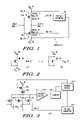
- FIG. 1is a schematic illustration of a pair of transistors that are connected to a voltage converter
- FIG. 2is a schematic diagram of a test circuit of a first type and a test circuit of a second type according to an embodiment of the invention
- FIG. 3is a schematic circuitry of a test circuitry according to an embodiment of the invention.
- FIG. 4is a graph illustrating two exemplary relationships between a voltage thresholds and a leakage current of a transistor
- FIG. 5is illustrates various stages of a test sequence, according to an embodiment of the invention.
- FIG. 6is a flow chart illustrating a method for biasing a transistor connected to a voltage converter, according to an embodiment of the invention.
- FIG. 7is a flow chart illustrating an operating sequence of the transistor according to an embodiment of the invention.
- a single voltage converterprovides multiple bias voltages such as Vnw and Vpw, but this is not necessarily so and these bias voltages can be provided by multiple voltage converters.
- FIG. 1illustrates an exemplary compensated circuit such as inverter 6 .
- the inverter 6can be a part of a processor that is positioned within a mobile device, but this is not necessarily so.
- Inverter 6includes an NMOS transistor (Mn) 20 , a PMOS transistor (Mp) 10 and a voltage converter 80 .
- Mn 20has a gate 22 , a source 24 , a drain 26 and a well 28 .
- Mp 10has a gate 12 , a source 14 , a drain 16 and a well 18 .
- Gates 12 and 22are connected to each other to form an input node 7 of inverter 6 while the drains 16 and 26 of both transistors are connected to form an output node 9 of inverter 6 .
- the source 14 of Mp 10is connected to a positive power supply (Vdd) 40 while the source 24 of Mn 20 is connected to a negative power supply (Vss) 50 .
- Vdd and Vssare provided to most of the components of the device that includes the inverter.
- both Mn and Mpare reversed well biased.
- the well 18 of Mp 10receives a bias voltage Vpw 60 that is more positive than Vdd 40 and the well 28 of Mn 20 receives a bias voltage Vnw 70 that is more negative than Vss 50 .
- These bias voltages (Vpw and Vnw)are provided by a voltage converter 80 that in turn receives as input Vdd 40 and Vss 50 .
- a typical voltage converteris a charge pump voltage converter, but this is not necessarily so.
- Other types of converterscan be used, including buck converters, boost converters, buck-boost converters, CUK converters, flyback converters, forward converters, and the like.
- the aggregate leakage current of the inverter 6includes a source drain leakage current (ILsd), a substrate leakage current (ILs) and a voltage converter current.
- the voltage converter currentis typically substantially smaller than ILsd and Ils.
- ILsis proportional to the bias voltage.
- ILsis a leakage current that flows through the well of the transistors and is drained from the voltage converter 80 . It is an output current of the voltage converter.
- ILsdis inversely proportional to the bias voltage (Vpw or Vnw).
- Vpwbias voltage
- This certain bias voltagediffers in response to various parameters including temperature, manufacturing (process) variants, supply voltage values, and the like. It may also change over time.
- the relationship between the aggregate leakage current of the inverter and the bias voltagehas a single minimum.
- the bias voltagethat minimizes the leakage current there is a need to find this minimum. It is noted that if other relationships exist other minimum (or even local minimum) locating algorithms can be applied.
- Each transistor typee.g. PMOS and NMOS
- the optimal Vpwthat results in a minimal PMOS transistor leakage current
- FIG. 2is a schematic diagram of a test circuit of a first type 101 and a test circuit of a second type 105 , according to an embodiment of the invention.
- NMOS test circuitsare illustrated, whereas equivalent test circuits for PMOS transistors are also utilized.
- PMOS transistorsthe NMOS transistors of test circuits 101 and 105 are replaced by PMOS transistors.
- a parameter, such as the leakage current of test circuit 101 ,is representative of ILsd.
- a parameter, such as the leakage current of test circuit 103 ,is representative of ILs.
- Test circuit 101includes an NMOS transistor 103 , having substantially the same characteristics of Mn 20 .
- the source of NMOS transistor 103is grounded and its gate and source of the NMOS transistor are connected to Vdd 40 .
- Test circuit 105includes an NMOS transistor 107 , having substantially the same characteristics of Mn 20 .
- the source, gate and drain of NMOS transistor 107are connected to Vdd 40 .
- the wells of NMOS transistors 103 and 107are connected to a bias voltage source Vb 109 .
- FIG. 3is a schematic circuitry of a test circuitry 100 according to an embodiment of the invention.
- Test circuitry 100measures a current that is representative of the aggregate leakage current of inventor 6 .
- the aggregate leakage currentis responsive to various leakage currents and to the efficiency of the voltage converter connected to the inverter.
- the test circuitryincludes multiple test circuits. In order to provide an indication about the aggregate leakage current the efficiency of the voltage converter must be taken into account. Thus, the ratio between the amount of test circuits of the first type and test circuit of the second type is responsive to Eff.
- the inventorsused a ratio of 2/(1/Eff ⁇ 1), but other ratios can be used.
- test circuitry 100includes two test circuits of the second type 101 and a single test circuit of the first type 102 . It is noted that the test circuitry 100 can include much more test circuits, as long as the ratio between test circuits of the two types remains.
- test circuitry 100includes NMOS transistors and that an equivalent test circuitry, including PMOS transistors, is also provided for PMOS transistors. Each test circuitry is activated in order to locate the corresponding optimal bias voltage. Test circuitry 100 is used to determine the optimal Vnw.
- the reduction of leakage currentis required during idle periods, as the decrement of the leakage current also slows the transistor. It is noted that this is not necessarily that the method can be applied for locating an optimal bias voltage under speed constraints. For example, if the transistor operates at a certain frequency and the bias voltage required for achieving that frequency is known, the method can be applied over a bias voltage region that starts by that certain bias voltage.
- the methodis performed whenever the compensated circuitry such as a processor that includes inverter 6 enters an idle state.
- the test circuitry 100is operated for minimizing leakage current at idle states thus is can operate at a very low frequency. By operating at very low frequencies the power consumption of the test circuitry is relative small and even negligent.
- the inventorsoperated the test circuitry at low frequencies of about 64 Khz, while the inverter 6 can operate at much higher frequencies (500 Mhz and above).
- Test circuitry 100provides an indication of the leakage current by connecting multiple test circuits 101 and 105 to a capacitor 120 , discharging the capacitor 120 by the leakage current of these test circuits, and providing an indication about the discharging period.
- the capacitor 120is connected to a drain of PMOS transistor 130 while the source of that PMOS transistor 130 is connected to Vdd 40 .
- the gate of the PMOS transistor 130receives a control signal from a control module 160 that turns the PMOS transistor 130 ON to charge the capacitor 120 and turns the PMOS transistor 130 OFF in order to discharge the capacitor 120 by the leakage currents of test circuits 101 and 105 .
- the sources of the NMOS transistors within the test circuitsare connected in parallel to each other and also to a voltage detector 140 that monitors the discharge of capacitor 120 via the test circuits.
- the voltage detector 140can compare the input voltage to a reference voltage to define when the capacitor has discharged to a predefined voltage level.
- the output of the voltage detector 140is connected to a counter 150 that measures the discharge period of capacitor 120 .
- the counter 150provides a timing signal indicative of the discharge period to a control module 160 .
- the control module 160is also connected to a voltage converter 170 that provides a bias voltage Vb to the transistors of the test circuits 101 and 105 .
- the voltage converter 170can also provide the bias voltage to the compensated circuit.
- the control module 160determines which bias voltage to provide during each iteration of a test sequence and also may determine when the sequence ends—for example, when an optimal bias voltage is found.
- test circuitry 100can be implemented by a relatively simple circuit with a simple control algorithm, as it locates a minimum of a relatively simple curve describing the relationship between current leakage and bias voltage. Furthermore, the test circuitry 100 does not have to store many measurement or to accurately measure the capacitor discharge period, as it can just determine if a current discharge period is larger than or smaller than a previous discharge period and in response either increase or decrease the bias voltage that is provided to the test circuits during a next test iteration.
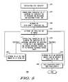
- FIG. 5is illustrates various stages of a test sequence 200 , according to an embodiment of the invention.
- Control module 160controls the execution of the test sequence 200 .
- Test sequence 200starts at stage 210 of initializing test circuitry 100 .
- This initializationmay includes providing a certain bias voltage Vb to the transistors of the test circuits 101 and 105 , resetting the counter 150 , resetting a pass counter value, and allowing the capacitor 120 to charge via PMOS transistor 130 , to a predefined voltage level, such as substantially Vdd-Vt.
- Stage 210is followed by stage 220 of turning PMOS transistor 130 OFF, allowing the capacitor 120 to discharge and measuring the discharge period T(n). This measurement is sent to the control module 160 and is stored for comparison with the next discharge period.
- Stage 220is followed by stage 230 of altering Vb (for example, increasing Vb) and jumping to stage 240 of allowing the capacitor 120 to charge.
- Stage 240is followed by stage 250 of turning PMOS transistor 130 OFF, allowing the capacitor 120 to discharge and measuring the discharge period T(n+1).
- Stage 250also includes comparing the current discharge period T(n) to the pervious discharge period T(n+1).
- stage 250is followed by stage 260 of altering Vb at the same manner as in stage 230 (for example—Vb id also increased). Stage 260 is followed by stage 240 .
- stage 270is followed by stage 280 of increasing a pass counter by one and checking if the pass counter equals two. If it equals two the test ends and the previous provided bias voltage is selected as the optimal bias voltage. Else, stage 270 is followed by stage 240 .
- FIG. 6is a flow chart illustrating method 300 for biasing a transistor connected to a voltage converter, according to an embodiment of the invention.
- Method 300starts by stage 310 of providing a test circuitry.
- the test circuitryincludes at least one test circuit of a first type and at least one test circuit of a second type; whereas a parameter of the test circuit of the first type is representative of first leakage current of the transistor and wherein a parameter of the test circuit of the second type is representative of the second leakage current of the transistor.
- a relationship between an amount of test circuit of the first type and an amount of a test circuit of the second typeis responsive to the at least one characteristic of the voltage converter.
- the characteristic of the voltage converteris a ratio between an input current of the voltage converter and an output current of the voltage converter.
- a test circuitry 100is provided, having test circuits of a first and second type 101 and 105 , whereas the ratio between the amount of the test circuits is responsive to Eff.
- Each test circuithas a leakage current that represents a leakage current of inverter 6 of FIG. 1 .
- Stage 310is followed by stage 320 of measuring at least one parameter of a test circuitry representative of at least one characteristic of the transistor and of at least one characteristic of the voltage converter.
- the measured parameteris a leakage current.
- one of the transistor characteristicsis responsive to the at least one characteristic of the voltage supply.
- the at least one characteristic of the transistoris at least two leakage currents.
- a first leakage currentis responsive to a characteristic of the voltage converter and wherein a second leakage current is substantially indifferent to the characteristic of the voltage converter.
- test circuitry 100includes test circuits that provide an indication about ILs/Eff and about ILsd.
- stage 320includes measuring a discharge period of a capacitor being discharged by leakage currents of the test circuitry.
- Stage 320is followed by stage 330 of determining if a certain control criterion was fulfilled.
- the control criterioncan be locating one or more optimal Vb.
- stage 330If the answer is positive stage 330 is followed by stage 350 of providing a voltage bias to a well of the transistor in response to the measurements. If the answer is negative stage 330 is followed by stage 340 of altering at least one bias voltage and jumping to stage 320 .
- FIG. 7is a flow chart illustrating an operating sequence 400 of the transistor according to an embodiment of the invention.
- Sequence 400starts by stage 410 of operating the transistor at a high-speed operational mode. During this stage the transistor is operated at a high speed. Typically, the transistor is a part of a processor and the high-speed operation is required when the processor executed a high computational load task.
- the control module 160receives an indication relating to the operational mode of the transistor but according to another embodiment of the invention can control that operational mode and determine what said mode is without receiving another indication.
- Vthas to be low, thus the voltage converter is disconnected from the well of the transistor.
- the wellcan receive bias voltages that do not exceed the power supplies Vdd and Vss.
- Stage 410is followed by stage 420 of altering the operational mode of the transistor to a low speed operational load and even to an idle mode.
- Stage 420is followed by stage 430 of determining a bias voltage to provide to the transistor during the low speed operational mode, entering the low speed operational load and biasing the transistor in response to the determination.
- stage 430includes a sequence of stages such as stages 310 – 350 .
- the voltage converteris activated to provide the required bias voltage.
- Stage 430is followed by altering the operational mode of the transistor and jumping to stage 410 .
- the voltage converteris usually disconnected from the transistor and a lower bias voltage is provided to the well of the transistor to allow faster operation.
Landscapes
- Engineering & Computer Science (AREA)
- Microelectronics & Electronic Packaging (AREA)
- Physics & Mathematics (AREA)
- General Physics & Mathematics (AREA)
- Testing Of Individual Semiconductor Devices (AREA)
- Tests Of Electronic Circuits (AREA)
- Semiconductor Integrated Circuits (AREA)
Abstract
Description
Claims (17)
Priority Applications (1)
| Application Number | Priority Date | Filing Date | Title |
|---|---|---|---|
| US10/955,219US7227366B2 (en) | 2004-09-30 | 2004-09-30 | Device and a method for biasing a transistor that is connected to a power converter |
Applications Claiming Priority (1)
| Application Number | Priority Date | Filing Date | Title |
|---|---|---|---|
| US10/955,219US7227366B2 (en) | 2004-09-30 | 2004-09-30 | Device and a method for biasing a transistor that is connected to a power converter |
Publications (2)
| Publication Number | Publication Date |
|---|---|
| US20060066316A1 US20060066316A1 (en) | 2006-03-30 |
| US7227366B2true US7227366B2 (en) | 2007-06-05 |
Family
ID=36098297
Family Applications (1)
| Application Number | Title | Priority Date | Filing Date |
|---|---|---|---|
| US10/955,219Expired - LifetimeUS7227366B2 (en) | 2004-09-30 | 2004-09-30 | Device and a method for biasing a transistor that is connected to a power converter |
Country Status (1)
| Country | Link |
|---|---|
| US (1) | US7227366B2 (en) |
Cited By (3)
| Publication number | Priority date | Publication date | Assignee | Title |
|---|---|---|---|---|
| US8742778B2 (en) | 2012-01-18 | 2014-06-03 | International Business Machines Corporation | Testing protection schemes of a power converter |
| US8918657B2 (en) | 2008-09-08 | 2014-12-23 | Virginia Tech Intellectual Properties | Systems, devices, and/or methods for managing energy usage |
| US20170155392A1 (en)* | 2014-05-19 | 2017-06-01 | Sony Corporation | Semiconductor apparatus and method of controlling mos transistor |
Families Citing this family (4)
| Publication number | Priority date | Publication date | Assignee | Title |
|---|---|---|---|---|
| CN103048636B (en)* | 2012-12-21 | 2015-07-08 | 深圳深爱半导体股份有限公司 | Transistor screening instrument calibration device |
| US9470719B2 (en)* | 2014-11-14 | 2016-10-18 | Cavium, Inc. | Testing semiconductor devices |
| US10705129B2 (en) | 2017-09-13 | 2020-07-07 | Toshiba Memory Corporation | Techniques for testing PLP capacitors |
| KR102551551B1 (en)* | 2018-08-28 | 2023-07-05 | 삼성전자주식회사 | Method of operating image sensor and image sensor performing the same |
Citations (3)
| Publication number | Priority date | Publication date | Assignee | Title |
|---|---|---|---|---|
| US20020005750A1 (en) | 1999-11-30 | 2002-01-17 | James T. Kao | Adaptive body biasing circuit and method |
| US20040113649A1 (en)* | 2002-08-30 | 2004-06-17 | Jorg Berthold | Semiconductor device for adjusting threshold value shift due to short channel effect |
| US6753719B2 (en)* | 2002-08-26 | 2004-06-22 | Motorola, Inc. | System and circuit for controlling well biasing and method thereof |
- 2004
- 2004-09-30USUS10/955,219patent/US7227366B2/ennot_activeExpired - Lifetime
Patent Citations (4)
| Publication number | Priority date | Publication date | Assignee | Title |
|---|---|---|---|---|
| US20020005750A1 (en) | 1999-11-30 | 2002-01-17 | James T. Kao | Adaptive body biasing circuit and method |
| US6448840B2 (en)* | 1999-11-30 | 2002-09-10 | Intel Corporation | Adaptive body biasing circuit and method |
| US6753719B2 (en)* | 2002-08-26 | 2004-06-22 | Motorola, Inc. | System and circuit for controlling well biasing and method thereof |
| US20040113649A1 (en)* | 2002-08-30 | 2004-06-17 | Jorg Berthold | Semiconductor device for adjusting threshold value shift due to short channel effect |
Cited By (4)
| Publication number | Priority date | Publication date | Assignee | Title |
|---|---|---|---|---|
| US8918657B2 (en) | 2008-09-08 | 2014-12-23 | Virginia Tech Intellectual Properties | Systems, devices, and/or methods for managing energy usage |
| US8742778B2 (en) | 2012-01-18 | 2014-06-03 | International Business Machines Corporation | Testing protection schemes of a power converter |
| US20170155392A1 (en)* | 2014-05-19 | 2017-06-01 | Sony Corporation | Semiconductor apparatus and method of controlling mos transistor |
| US10263622B2 (en)* | 2014-05-19 | 2019-04-16 | Sony Semiconductor Solutions Corporation | Semiconductor apparatus and method of controlling MOS transistor |
Also Published As
| Publication number | Publication date |
|---|---|
| US20060066316A1 (en) | 2006-03-30 |
Similar Documents
| Publication | Publication Date | Title |
|---|---|---|
| US8912778B1 (en) | Switching voltage regulator employing current pre-adjust based on power mode | |
| US7375503B2 (en) | System for current sensing in switched DC-to-DC converters | |
| US7781909B2 (en) | Control circuit of power supply, power supply and control method thereof | |
| US6943533B2 (en) | Voltage conversion circuit, semiconductor integrated circuit device, and portable terminal | |
| US20070030044A1 (en) | Supply tracking clock multiplier | |
| US20100156366A1 (en) | Step-down switching regulator, control circuit thereof, and electronic device using the same | |
| US20060193157A1 (en) | Thermal compensation method for CMOS digital-integrated circuits using temperature-adaptive digital DC/DC converter | |
| US20210124383A1 (en) | Techniques for low-dropout (ldo) regulator start-up detection | |
| US7902914B2 (en) | Semiconductor integrated circuit | |
| US6731158B1 (en) | Self regulating body bias generator | |
| US12027904B2 (en) | Systems and methods for low current detection | |
| US7847622B2 (en) | Electric circuit device | |
| KR100334363B1 (en) | Power supply apparatus | |
| US11398813B2 (en) | Integrated oscillator | |
| US7227366B2 (en) | Device and a method for biasing a transistor that is connected to a power converter | |
| US6809577B2 (en) | Semiconductor integrated circuit having internal power supply voltage down conversion circuit | |
| US8836414B2 (en) | Device and method for compensating for voltage drops | |
| US20100295530A1 (en) | Power supply voltage control circuit | |
| US20240055991A1 (en) | Techniques for operating a switched-mode power supply | |
| US8209558B2 (en) | System and method for controlling voltage and frequency in a multiple voltage environment | |
| US6750694B1 (en) | Signal clipping circuit | |
| US6810497B2 (en) | Semiconductor integrated circuit compensating variations of delay time | |
| JP2007151322A (en) | Power circuit and dc-dc converter | |
| US6486730B1 (en) | Voltage down pump and method of operation | |
| KR102775271B1 (en) | Power supply circuit with low quiescent current in bypass mode |
Legal Events
| Date | Code | Title | Description |
|---|---|---|---|
| AS | Assignment | Owner name:FREESCALE SEMICONDUCTOR, INC., TEXAS Free format text:ASSIGNMENT OF ASSIGNORS INTEREST;ASSIGNORS:ROZEN, ANTON;KUZMIN, DAN;PRIEL, MICHAEL;REEL/FRAME:015582/0589 Effective date:20041111 | |
| AS | Assignment | Owner name:CITIBANK, N.A. AS COLLATERAL AGENT, NEW YORK Free format text:SECURITY AGREEMENT;ASSIGNORS:FREESCALE SEMICONDUCTOR, INC.;FREESCALE ACQUISITION CORPORATION;FREESCALE ACQUISITION HOLDINGS CORP.;AND OTHERS;REEL/FRAME:018855/0129 Effective date:20061201 Owner name:CITIBANK, N.A. AS COLLATERAL AGENT,NEW YORK Free format text:SECURITY AGREEMENT;ASSIGNORS:FREESCALE SEMICONDUCTOR, INC.;FREESCALE ACQUISITION CORPORATION;FREESCALE ACQUISITION HOLDINGS CORP.;AND OTHERS;REEL/FRAME:018855/0129 Effective date:20061201 | |
| STCF | Information on status: patent grant | Free format text:PATENTED CASE | |
| AS | Assignment | Owner name:CITIBANK, N.A., AS COLLATERAL AGENT, NEW YORK Free format text:SECURITY AGREEMENT;ASSIGNOR:FREESCALE SEMICONDUCTOR, INC.;REEL/FRAME:020045/0448 Effective date:20070718 Owner name:CITIBANK, N.A., AS COLLATERAL AGENT,NEW YORK Free format text:SECURITY AGREEMENT;ASSIGNOR:FREESCALE SEMICONDUCTOR, INC.;REEL/FRAME:020045/0448 Effective date:20070718 | |
| AS | Assignment | Owner name:CITIBANK, N.A., AS COLLATERAL AGENT,NEW YORK Free format text:SECURITY AGREEMENT;ASSIGNOR:FREESCALE SEMICONDUCTOR, INC.;REEL/FRAME:024397/0001 Effective date:20100413 Owner name:CITIBANK, N.A., AS COLLATERAL AGENT, NEW YORK Free format text:SECURITY AGREEMENT;ASSIGNOR:FREESCALE SEMICONDUCTOR, INC.;REEL/FRAME:024397/0001 Effective date:20100413 | |
| FPAY | Fee payment | Year of fee payment:4 | |
| AS | Assignment | Owner name:CITIBANK, N.A., AS NOTES COLLATERAL AGENT, NEW YORK Free format text:SECURITY AGREEMENT;ASSIGNOR:FREESCALE SEMICONDUCTOR, INC.;REEL/FRAME:030633/0424 Effective date:20130521 Owner name:CITIBANK, N.A., AS NOTES COLLATERAL AGENT, NEW YOR Free format text:SECURITY AGREEMENT;ASSIGNOR:FREESCALE SEMICONDUCTOR, INC.;REEL/FRAME:030633/0424 Effective date:20130521 | |
| AS | Assignment | Owner name:CITIBANK, N.A., AS NOTES COLLATERAL AGENT, NEW YORK Free format text:SECURITY AGREEMENT;ASSIGNOR:FREESCALE SEMICONDUCTOR, INC.;REEL/FRAME:031591/0266 Effective date:20131101 Owner name:CITIBANK, N.A., AS NOTES COLLATERAL AGENT, NEW YOR Free format text:SECURITY AGREEMENT;ASSIGNOR:FREESCALE SEMICONDUCTOR, INC.;REEL/FRAME:031591/0266 Effective date:20131101 | |
| FPAY | Fee payment | Year of fee payment:8 | |
| AS | Assignment | Owner name:FREESCALE SEMICONDUCTOR, INC., TEXAS Free format text:PATENT RELEASE;ASSIGNOR:CITIBANK, N.A., AS COLLATERAL AGENT;REEL/FRAME:037354/0225 Effective date:20151207 Owner name:FREESCALE SEMICONDUCTOR, INC., TEXAS Free format text:PATENT RELEASE;ASSIGNOR:CITIBANK, N.A., AS COLLATERAL AGENT;REEL/FRAME:037354/0655 Effective date:20151207 Owner name:FREESCALE SEMICONDUCTOR, INC., TEXAS Free format text:PATENT RELEASE;ASSIGNOR:CITIBANK, N.A., AS COLLATERAL AGENT;REEL/FRAME:037356/0553 Effective date:20151207 Owner name:FREESCALE SEMICONDUCTOR, INC., TEXAS Free format text:PATENT RELEASE;ASSIGNOR:CITIBANK, N.A., AS COLLATERAL AGENT;REEL/FRAME:037356/0143 Effective date:20151207 | |
| AS | Assignment | Owner name:MORGAN STANLEY SENIOR FUNDING, INC., MARYLAND Free format text:ASSIGNMENT AND ASSUMPTION OF SECURITY INTEREST IN PATENTS;ASSIGNOR:CITIBANK, N.A.;REEL/FRAME:037486/0517 Effective date:20151207 | |
| AS | Assignment | Owner name:MORGAN STANLEY SENIOR FUNDING, INC., MARYLAND Free format text:ASSIGNMENT AND ASSUMPTION OF SECURITY INTEREST IN PATENTS;ASSIGNOR:CITIBANK, N.A.;REEL/FRAME:037518/0292 Effective date:20151207 | |
| AS | Assignment | Owner name:MORGAN STANLEY SENIOR FUNDING, INC., MARYLAND Free format text:SUPPLEMENT TO THE SECURITY AGREEMENT;ASSIGNOR:FREESCALE SEMICONDUCTOR, INC.;REEL/FRAME:039138/0001 Effective date:20160525 | |
| AS | Assignment | Owner name:NXP, B.V., F/K/A FREESCALE SEMICONDUCTOR, INC., NETHERLANDS Free format text:RELEASE BY SECURED PARTY;ASSIGNOR:MORGAN STANLEY SENIOR FUNDING, INC.;REEL/FRAME:040925/0001 Effective date:20160912 Owner name:NXP, B.V., F/K/A FREESCALE SEMICONDUCTOR, INC., NE Free format text:RELEASE BY SECURED PARTY;ASSIGNOR:MORGAN STANLEY SENIOR FUNDING, INC.;REEL/FRAME:040925/0001 Effective date:20160912 | |
| AS | Assignment | Owner name:NXP B.V., NETHERLANDS Free format text:RELEASE BY SECURED PARTY;ASSIGNOR:MORGAN STANLEY SENIOR FUNDING, INC.;REEL/FRAME:040928/0001 Effective date:20160622 | |
| AS | Assignment | Owner name:NXP USA, INC., TEXAS Free format text:CHANGE OF NAME;ASSIGNOR:FREESCALE SEMICONDUCTOR INC.;REEL/FRAME:040652/0180 Effective date:20161107 | |
| AS | Assignment | Owner name:NXP USA, INC., TEXAS Free format text:CORRECTIVE ASSIGNMENT TO CORRECT THE NATURE OF CONVEYANCE LISTED CHANGE OF NAME SHOULD BE MERGER AND CHANGE PREVIOUSLY RECORDED AT REEL: 040652 FRAME: 0180. ASSIGNOR(S) HEREBY CONFIRMS THE MERGER AND CHANGE OF NAME;ASSIGNOR:FREESCALE SEMICONDUCTOR INC.;REEL/FRAME:041354/0148 Effective date:20161107 | |
| AS | Assignment | Owner name:MORGAN STANLEY SENIOR FUNDING, INC., MARYLAND Free format text:CORRECTIVE ASSIGNMENT TO CORRECT THE REMOVE PATENTS 8108266 AND 8062324 AND REPLACE THEM WITH 6108266 AND 8060324 PREVIOUSLY RECORDED ON REEL 037518 FRAME 0292. ASSIGNOR(S) HEREBY CONFIRMS THE ASSIGNMENT AND ASSUMPTION OF SECURITY INTEREST IN PATENTS;ASSIGNOR:CITIBANK, N.A.;REEL/FRAME:041703/0536 Effective date:20151207 | |
| AS | Assignment | Owner name:VLSI TECHNOLOGY LLC, DELAWARE Free format text:ASSIGNMENT OF ASSIGNORS INTEREST;ASSIGNOR:NXP USA, INC.;REEL/FRAME:045084/0184 Effective date:20171204 | |
| MAFP | Maintenance fee payment | Free format text:PAYMENT OF MAINTENANCE FEE, 12TH YEAR, LARGE ENTITY (ORIGINAL EVENT CODE: M1553); ENTITY STATUS OF PATENT OWNER: LARGE ENTITY Year of fee payment:12 | |
| AS | Assignment | Owner name:SHENZHEN XINGUODU TECHNOLOGY CO., LTD., CHINA Free format text:CORRECTIVE ASSIGNMENT TO CORRECT THE TO CORRECT THE APPLICATION NO. FROM 13,883,290 TO 13,833,290 PREVIOUSLY RECORDED ON REEL 041703 FRAME 0536. ASSIGNOR(S) HEREBY CONFIRMS THE THE ASSIGNMENT AND ASSUMPTION OF SECURITYINTEREST IN PATENTS.;ASSIGNOR:MORGAN STANLEY SENIOR FUNDING, INC.;REEL/FRAME:048734/0001 Effective date:20190217 | |
| AS | Assignment | Owner name:NXP B.V., NETHERLANDS Free format text:RELEASE BY SECURED PARTY;ASSIGNOR:MORGAN STANLEY SENIOR FUNDING, INC.;REEL/FRAME:050744/0097 Effective date:20190903 | |
| AS | Assignment | Owner name:MORGAN STANLEY SENIOR FUNDING, INC., MARYLAND Free format text:CORRECTIVE ASSIGNMENT TO CORRECT THE REMOVE APPLICATION11759915 AND REPLACE IT WITH APPLICATION 11759935 PREVIOUSLY RECORDED ON REEL 037486 FRAME 0517. ASSIGNOR(S) HEREBY CONFIRMS THE ASSIGNMENT AND ASSUMPTION OF SECURITYINTEREST IN PATENTS;ASSIGNOR:CITIBANK, N.A.;REEL/FRAME:053547/0421 Effective date:20151207 | |
| AS | Assignment | Owner name:NXP B.V., NETHERLANDS Free format text:CORRECTIVE ASSIGNMENT TO CORRECT THE REMOVEAPPLICATION 11759915 AND REPLACE IT WITH APPLICATION11759935 PREVIOUSLY RECORDED ON REEL 040928 FRAME 0001. ASSIGNOR(S) HEREBY CONFIRMS THE RELEASE OF SECURITYINTEREST;ASSIGNOR:MORGAN STANLEY SENIOR FUNDING, INC.;REEL/FRAME:052915/0001 Effective date:20160622 | |
| AS | Assignment | Owner name:NXP, B.V. F/K/A FREESCALE SEMICONDUCTOR, INC., NETHERLANDS Free format text:CORRECTIVE ASSIGNMENT TO CORRECT THE REMOVEAPPLICATION 11759915 AND REPLACE IT WITH APPLICATION11759935 PREVIOUSLY RECORDED ON REEL 040925 FRAME 0001. ASSIGNOR(S) HEREBY CONFIRMS THE RELEASE OF SECURITYINTEREST;ASSIGNOR:MORGAN STANLEY SENIOR FUNDING, INC.;REEL/FRAME:052917/0001 Effective date:20160912 |