US7227240B2 - Semiconductor device with wire bond inductor and method - Google Patents
Semiconductor device with wire bond inductor and methodDownload PDFInfo
- Publication number
- US7227240B2 US7227240B2US10/524,894US52489405AUS7227240B2US 7227240 B2US7227240 B2US 7227240B2US 52489405 AUS52489405 AUS 52489405AUS 7227240 B2US7227240 B2US 7227240B2
- Authority
- US
- United States
- Prior art keywords
- inductor
- semiconductor device
- bonding wire
- bonding
- semiconductor
- Prior art date
- Legal status (The legal status is an assumption and is not a legal conclusion. Google has not performed a legal analysis and makes no representation as to the accuracy of the status listed.)
- Expired - Lifetime
Links
Images


Classifications
- H—ELECTRICITY
- H01—ELECTRIC ELEMENTS
- H01L—SEMICONDUCTOR DEVICES NOT COVERED BY CLASS H10
- H01L24/00—Arrangements for connecting or disconnecting semiconductor or solid-state bodies; Methods or apparatus related thereto
- H01L24/80—Methods for connecting semiconductor or other solid state bodies using means for bonding being attached to, or being formed on, the surface to be connected
- H01L24/85—Methods for connecting semiconductor or other solid state bodies using means for bonding being attached to, or being formed on, the surface to be connected using a wire connector
- H—ELECTRICITY
- H01—ELECTRIC ELEMENTS
- H01L—SEMICONDUCTOR DEVICES NOT COVERED BY CLASS H10
- H01L23/00—Details of semiconductor or other solid state devices
- H01L23/48—Arrangements for conducting electric current to or from the solid state body in operation, e.g. leads, terminal arrangements ; Selection of materials therefor
- H01L23/488—Arrangements for conducting electric current to or from the solid state body in operation, e.g. leads, terminal arrangements ; Selection of materials therefor consisting of soldered or bonded constructions
- H01L23/495—Lead-frames or other flat leads
- H01L23/49517—Additional leads
- H01L23/4952—Additional leads the additional leads being a bump or a wire
- H—ELECTRICITY
- H01—ELECTRIC ELEMENTS
- H01L—SEMICONDUCTOR DEVICES NOT COVERED BY CLASS H10
- H01L24/00—Arrangements for connecting or disconnecting semiconductor or solid-state bodies; Methods or apparatus related thereto
- H01L24/01—Means for bonding being attached to, or being formed on, the surface to be connected, e.g. chip-to-package, die-attach, "first-level" interconnects; Manufacturing methods related thereto
- H01L24/42—Wire connectors; Manufacturing methods related thereto
- H01L24/47—Structure, shape, material or disposition of the wire connectors after the connecting process
- H01L24/48—Structure, shape, material or disposition of the wire connectors after the connecting process of an individual wire connector
- H—ELECTRICITY
- H01—ELECTRIC ELEMENTS
- H01L—SEMICONDUCTOR DEVICES NOT COVERED BY CLASS H10
- H01L2224/00—Indexing scheme for arrangements for connecting or disconnecting semiconductor or solid-state bodies and methods related thereto as covered by H01L24/00
- H01L2224/01—Means for bonding being attached to, or being formed on, the surface to be connected, e.g. chip-to-package, die-attach, "first-level" interconnects; Manufacturing methods related thereto
- H01L2224/02—Bonding areas; Manufacturing methods related thereto
- H01L2224/04—Structure, shape, material or disposition of the bonding areas prior to the connecting process
- H01L2224/05—Structure, shape, material or disposition of the bonding areas prior to the connecting process of an individual bonding area
- H01L2224/0554—External layer
- H01L2224/0555—Shape
- H01L2224/05552—Shape in top view
- H01L2224/05553—Shape in top view being rectangular
- H—ELECTRICITY
- H01—ELECTRIC ELEMENTS
- H01L—SEMICONDUCTOR DEVICES NOT COVERED BY CLASS H10
- H01L2224/00—Indexing scheme for arrangements for connecting or disconnecting semiconductor or solid-state bodies and methods related thereto as covered by H01L24/00
- H01L2224/01—Means for bonding being attached to, or being formed on, the surface to be connected, e.g. chip-to-package, die-attach, "first-level" interconnects; Manufacturing methods related thereto
- H01L2224/42—Wire connectors; Manufacturing methods related thereto
- H01L2224/44—Structure, shape, material or disposition of the wire connectors prior to the connecting process
- H01L2224/45—Structure, shape, material or disposition of the wire connectors prior to the connecting process of an individual wire connector
- H01L2224/45001—Core members of the connector
- H01L2224/4501—Shape
- H01L2224/45012—Cross-sectional shape
- H01L2224/45015—Cross-sectional shape being circular
- H—ELECTRICITY
- H01—ELECTRIC ELEMENTS
- H01L—SEMICONDUCTOR DEVICES NOT COVERED BY CLASS H10
- H01L2224/00—Indexing scheme for arrangements for connecting or disconnecting semiconductor or solid-state bodies and methods related thereto as covered by H01L24/00
- H01L2224/01—Means for bonding being attached to, or being formed on, the surface to be connected, e.g. chip-to-package, die-attach, "first-level" interconnects; Manufacturing methods related thereto
- H01L2224/42—Wire connectors; Manufacturing methods related thereto
- H01L2224/44—Structure, shape, material or disposition of the wire connectors prior to the connecting process
- H01L2224/45—Structure, shape, material or disposition of the wire connectors prior to the connecting process of an individual wire connector
- H01L2224/45001—Core members of the connector
- H01L2224/45099—Material
- H01L2224/451—Material with a principal constituent of the material being a metal or a metalloid, e.g. boron (B), silicon (Si), germanium (Ge), arsenic (As), antimony (Sb), tellurium (Te) and polonium (Po), and alloys thereof
- H01L2224/45117—Material with a principal constituent of the material being a metal or a metalloid, e.g. boron (B), silicon (Si), germanium (Ge), arsenic (As), antimony (Sb), tellurium (Te) and polonium (Po), and alloys thereof the principal constituent melting at a temperature of greater than or equal to 400°C and less than 950°C
- H01L2224/45124—Aluminium (Al) as principal constituent
- H—ELECTRICITY
- H01—ELECTRIC ELEMENTS
- H01L—SEMICONDUCTOR DEVICES NOT COVERED BY CLASS H10
- H01L2224/00—Indexing scheme for arrangements for connecting or disconnecting semiconductor or solid-state bodies and methods related thereto as covered by H01L24/00
- H01L2224/01—Means for bonding being attached to, or being formed on, the surface to be connected, e.g. chip-to-package, die-attach, "first-level" interconnects; Manufacturing methods related thereto
- H01L2224/42—Wire connectors; Manufacturing methods related thereto
- H01L2224/44—Structure, shape, material or disposition of the wire connectors prior to the connecting process
- H01L2224/45—Structure, shape, material or disposition of the wire connectors prior to the connecting process of an individual wire connector
- H01L2224/45001—Core members of the connector
- H01L2224/45099—Material
- H01L2224/451—Material with a principal constituent of the material being a metal or a metalloid, e.g. boron (B), silicon (Si), germanium (Ge), arsenic (As), antimony (Sb), tellurium (Te) and polonium (Po), and alloys thereof
- H01L2224/45138—Material with a principal constituent of the material being a metal or a metalloid, e.g. boron (B), silicon (Si), germanium (Ge), arsenic (As), antimony (Sb), tellurium (Te) and polonium (Po), and alloys thereof the principal constituent melting at a temperature of greater than or equal to 950°C and less than 1550°C
- H01L2224/45144—Gold (Au) as principal constituent
- H—ELECTRICITY
- H01—ELECTRIC ELEMENTS
- H01L—SEMICONDUCTOR DEVICES NOT COVERED BY CLASS H10
- H01L2224/00—Indexing scheme for arrangements for connecting or disconnecting semiconductor or solid-state bodies and methods related thereto as covered by H01L24/00
- H01L2224/01—Means for bonding being attached to, or being formed on, the surface to be connected, e.g. chip-to-package, die-attach, "first-level" interconnects; Manufacturing methods related thereto
- H01L2224/42—Wire connectors; Manufacturing methods related thereto
- H01L2224/44—Structure, shape, material or disposition of the wire connectors prior to the connecting process
- H01L2224/45—Structure, shape, material or disposition of the wire connectors prior to the connecting process of an individual wire connector
- H01L2224/45001—Core members of the connector
- H01L2224/45099—Material
- H01L2224/451—Material with a principal constituent of the material being a metal or a metalloid, e.g. boron (B), silicon (Si), germanium (Ge), arsenic (As), antimony (Sb), tellurium (Te) and polonium (Po), and alloys thereof
- H01L2224/45138—Material with a principal constituent of the material being a metal or a metalloid, e.g. boron (B), silicon (Si), germanium (Ge), arsenic (As), antimony (Sb), tellurium (Te) and polonium (Po), and alloys thereof the principal constituent melting at a temperature of greater than or equal to 950°C and less than 1550°C
- H01L2224/45147—Copper (Cu) as principal constituent
- H—ELECTRICITY
- H01—ELECTRIC ELEMENTS
- H01L—SEMICONDUCTOR DEVICES NOT COVERED BY CLASS H10
- H01L2224/00—Indexing scheme for arrangements for connecting or disconnecting semiconductor or solid-state bodies and methods related thereto as covered by H01L24/00
- H01L2224/01—Means for bonding being attached to, or being formed on, the surface to be connected, e.g. chip-to-package, die-attach, "first-level" interconnects; Manufacturing methods related thereto
- H01L2224/42—Wire connectors; Manufacturing methods related thereto
- H01L2224/47—Structure, shape, material or disposition of the wire connectors after the connecting process
- H01L2224/48—Structure, shape, material or disposition of the wire connectors after the connecting process of an individual wire connector
- H01L2224/4805—Shape
- H01L2224/4809—Loop shape
- H01L2224/48091—Arched
- H—ELECTRICITY
- H01—ELECTRIC ELEMENTS
- H01L—SEMICONDUCTOR DEVICES NOT COVERED BY CLASS H10
- H01L2224/00—Indexing scheme for arrangements for connecting or disconnecting semiconductor or solid-state bodies and methods related thereto as covered by H01L24/00
- H01L2224/01—Means for bonding being attached to, or being formed on, the surface to be connected, e.g. chip-to-package, die-attach, "first-level" interconnects; Manufacturing methods related thereto
- H01L2224/42—Wire connectors; Manufacturing methods related thereto
- H01L2224/47—Structure, shape, material or disposition of the wire connectors after the connecting process
- H01L2224/48—Structure, shape, material or disposition of the wire connectors after the connecting process of an individual wire connector
- H01L2224/481—Disposition
- H01L2224/4813—Connecting within a semiconductor or solid-state body, i.e. fly wire, bridge wire
- H—ELECTRICITY
- H01—ELECTRIC ELEMENTS
- H01L—SEMICONDUCTOR DEVICES NOT COVERED BY CLASS H10
- H01L2224/00—Indexing scheme for arrangements for connecting or disconnecting semiconductor or solid-state bodies and methods related thereto as covered by H01L24/00
- H01L2224/01—Means for bonding being attached to, or being formed on, the surface to be connected, e.g. chip-to-package, die-attach, "first-level" interconnects; Manufacturing methods related thereto
- H01L2224/42—Wire connectors; Manufacturing methods related thereto
- H01L2224/47—Structure, shape, material or disposition of the wire connectors after the connecting process
- H01L2224/48—Structure, shape, material or disposition of the wire connectors after the connecting process of an individual wire connector
- H01L2224/481—Disposition
- H01L2224/48151—Connecting between a semiconductor or solid-state body and an item not being a semiconductor or solid-state body, e.g. chip-to-substrate, chip-to-passive
- H01L2224/48221—Connecting between a semiconductor or solid-state body and an item not being a semiconductor or solid-state body, e.g. chip-to-substrate, chip-to-passive the body and the item being stacked
- H01L2224/48245—Connecting between a semiconductor or solid-state body and an item not being a semiconductor or solid-state body, e.g. chip-to-substrate, chip-to-passive the body and the item being stacked the item being metallic
- H01L2224/48247—Connecting between a semiconductor or solid-state body and an item not being a semiconductor or solid-state body, e.g. chip-to-substrate, chip-to-passive the body and the item being stacked the item being metallic connecting the wire to a bond pad of the item
- H—ELECTRICITY
- H01—ELECTRIC ELEMENTS
- H01L—SEMICONDUCTOR DEVICES NOT COVERED BY CLASS H10
- H01L2224/00—Indexing scheme for arrangements for connecting or disconnecting semiconductor or solid-state bodies and methods related thereto as covered by H01L24/00
- H01L2224/01—Means for bonding being attached to, or being formed on, the surface to be connected, e.g. chip-to-package, die-attach, "first-level" interconnects; Manufacturing methods related thereto
- H01L2224/42—Wire connectors; Manufacturing methods related thereto
- H01L2224/47—Structure, shape, material or disposition of the wire connectors after the connecting process
- H01L2224/48—Structure, shape, material or disposition of the wire connectors after the connecting process of an individual wire connector
- H01L2224/484—Connecting portions
- H—ELECTRICITY
- H01—ELECTRIC ELEMENTS
- H01L—SEMICONDUCTOR DEVICES NOT COVERED BY CLASS H10
- H01L2224/00—Indexing scheme for arrangements for connecting or disconnecting semiconductor or solid-state bodies and methods related thereto as covered by H01L24/00
- H01L2224/01—Means for bonding being attached to, or being formed on, the surface to be connected, e.g. chip-to-package, die-attach, "first-level" interconnects; Manufacturing methods related thereto
- H01L2224/42—Wire connectors; Manufacturing methods related thereto
- H01L2224/47—Structure, shape, material or disposition of the wire connectors after the connecting process
- H01L2224/48—Structure, shape, material or disposition of the wire connectors after the connecting process of an individual wire connector
- H01L2224/485—Material
- H01L2224/48505—Material at the bonding interface
- H01L2224/48599—Principal constituent of the connecting portion of the wire connector being Gold (Au)
- H—ELECTRICITY
- H01—ELECTRIC ELEMENTS
- H01L—SEMICONDUCTOR DEVICES NOT COVERED BY CLASS H10
- H01L2224/00—Indexing scheme for arrangements for connecting or disconnecting semiconductor or solid-state bodies and methods related thereto as covered by H01L24/00
- H01L2224/01—Means for bonding being attached to, or being formed on, the surface to be connected, e.g. chip-to-package, die-attach, "first-level" interconnects; Manufacturing methods related thereto
- H01L2224/42—Wire connectors; Manufacturing methods related thereto
- H01L2224/47—Structure, shape, material or disposition of the wire connectors after the connecting process
- H01L2224/48—Structure, shape, material or disposition of the wire connectors after the connecting process of an individual wire connector
- H01L2224/485—Material
- H01L2224/48505—Material at the bonding interface
- H01L2224/48699—Principal constituent of the connecting portion of the wire connector being Aluminium (Al)
- H—ELECTRICITY
- H01—ELECTRIC ELEMENTS
- H01L—SEMICONDUCTOR DEVICES NOT COVERED BY CLASS H10
- H01L2224/00—Indexing scheme for arrangements for connecting or disconnecting semiconductor or solid-state bodies and methods related thereto as covered by H01L24/00
- H01L2224/74—Apparatus for manufacturing arrangements for connecting or disconnecting semiconductor or solid-state bodies and for methods related thereto
- H01L2224/78—Apparatus for connecting with wire connectors
- H01L2224/7825—Means for applying energy, e.g. heating means
- H01L2224/783—Means for applying energy, e.g. heating means by means of pressure
- H01L2224/78301—Capillary
- H—ELECTRICITY
- H01—ELECTRIC ELEMENTS
- H01L—SEMICONDUCTOR DEVICES NOT COVERED BY CLASS H10
- H01L2224/00—Indexing scheme for arrangements for connecting or disconnecting semiconductor or solid-state bodies and methods related thereto as covered by H01L24/00
- H01L2224/80—Methods for connecting semiconductor or other solid state bodies using means for bonding being attached to, or being formed on, the surface to be connected
- H01L2224/85—Methods for connecting semiconductor or other solid state bodies using means for bonding being attached to, or being formed on, the surface to be connected using a wire connector
- H01L2224/85009—Pre-treatment of the connector or the bonding area
- H01L2224/8503—Reshaping, e.g. forming the ball or the wedge of the wire connector
- H01L2224/85047—Reshaping, e.g. forming the ball or the wedge of the wire connector by mechanical means, e.g. severing, pressing, stamping
- H—ELECTRICITY
- H01—ELECTRIC ELEMENTS
- H01L—SEMICONDUCTOR DEVICES NOT COVERED BY CLASS H10
- H01L2224/00—Indexing scheme for arrangements for connecting or disconnecting semiconductor or solid-state bodies and methods related thereto as covered by H01L24/00
- H01L2224/80—Methods for connecting semiconductor or other solid state bodies using means for bonding being attached to, or being formed on, the surface to be connected
- H01L2224/85—Methods for connecting semiconductor or other solid state bodies using means for bonding being attached to, or being formed on, the surface to be connected using a wire connector
- H01L2224/8512—Aligning
- H01L2224/85148—Aligning involving movement of a part of the bonding apparatus
- H01L2224/85169—Aligning involving movement of a part of the bonding apparatus being the upper part of the bonding apparatus, i.e. bonding head, e.g. capillary or wedge
- H01L2224/8517—Rotational movements
- H—ELECTRICITY
- H01—ELECTRIC ELEMENTS
- H01L—SEMICONDUCTOR DEVICES NOT COVERED BY CLASS H10
- H01L2224/00—Indexing scheme for arrangements for connecting or disconnecting semiconductor or solid-state bodies and methods related thereto as covered by H01L24/00
- H01L2224/80—Methods for connecting semiconductor or other solid state bodies using means for bonding being attached to, or being formed on, the surface to be connected
- H01L2224/85—Methods for connecting semiconductor or other solid state bodies using means for bonding being attached to, or being formed on, the surface to be connected using a wire connector
- H01L2224/8512—Aligning
- H01L2224/85148—Aligning involving movement of a part of the bonding apparatus
- H01L2224/85169—Aligning involving movement of a part of the bonding apparatus being the upper part of the bonding apparatus, i.e. bonding head, e.g. capillary or wedge
- H01L2224/8518—Translational movements
- H01L2224/85181—Translational movements connecting first on the semiconductor or solid-state body, i.e. on-chip, regular stitch
- H—ELECTRICITY
- H01—ELECTRIC ELEMENTS
- H01L—SEMICONDUCTOR DEVICES NOT COVERED BY CLASS H10
- H01L23/00—Details of semiconductor or other solid state devices
- H01L23/52—Arrangements for conducting electric current within the device in operation from one component to another, i.e. interconnections, e.g. wires, lead frames
- H01L23/522—Arrangements for conducting electric current within the device in operation from one component to another, i.e. interconnections, e.g. wires, lead frames including external interconnections consisting of a multilayer structure of conductive and insulating layers inseparably formed on the semiconductor body
- H01L23/5227—Inductive arrangements or effects of, or between, wiring layers
- H—ELECTRICITY
- H01—ELECTRIC ELEMENTS
- H01L—SEMICONDUCTOR DEVICES NOT COVERED BY CLASS H10
- H01L24/00—Arrangements for connecting or disconnecting semiconductor or solid-state bodies; Methods or apparatus related thereto
- H01L24/01—Means for bonding being attached to, or being formed on, the surface to be connected, e.g. chip-to-package, die-attach, "first-level" interconnects; Manufacturing methods related thereto
- H01L24/42—Wire connectors; Manufacturing methods related thereto
- H01L24/44—Structure, shape, material or disposition of the wire connectors prior to the connecting process
- H01L24/45—Structure, shape, material or disposition of the wire connectors prior to the connecting process of an individual wire connector
- H—ELECTRICITY
- H01—ELECTRIC ELEMENTS
- H01L—SEMICONDUCTOR DEVICES NOT COVERED BY CLASS H10
- H01L24/00—Arrangements for connecting or disconnecting semiconductor or solid-state bodies; Methods or apparatus related thereto
- H01L24/74—Apparatus for manufacturing arrangements for connecting or disconnecting semiconductor or solid-state bodies
- H01L24/78—Apparatus for connecting with wire connectors
- H—ELECTRICITY
- H01—ELECTRIC ELEMENTS
- H01L—SEMICONDUCTOR DEVICES NOT COVERED BY CLASS H10
- H01L2924/00—Indexing scheme for arrangements or methods for connecting or disconnecting semiconductor or solid-state bodies as covered by H01L24/00
- H01L2924/0001—Technical content checked by a classifier
- H01L2924/00014—Technical content checked by a classifier the subject-matter covered by the group, the symbol of which is combined with the symbol of this group, being disclosed without further technical details
- H—ELECTRICITY
- H01—ELECTRIC ELEMENTS
- H01L—SEMICONDUCTOR DEVICES NOT COVERED BY CLASS H10
- H01L2924/00—Indexing scheme for arrangements or methods for connecting or disconnecting semiconductor or solid-state bodies as covered by H01L24/00
- H01L2924/01—Chemical elements
- H01L2924/01013—Aluminum [Al]
- H—ELECTRICITY
- H01—ELECTRIC ELEMENTS
- H01L—SEMICONDUCTOR DEVICES NOT COVERED BY CLASS H10
- H01L2924/00—Indexing scheme for arrangements or methods for connecting or disconnecting semiconductor or solid-state bodies as covered by H01L24/00
- H01L2924/01—Chemical elements
- H01L2924/01014—Silicon [Si]
- H—ELECTRICITY
- H01—ELECTRIC ELEMENTS
- H01L—SEMICONDUCTOR DEVICES NOT COVERED BY CLASS H10
- H01L2924/00—Indexing scheme for arrangements or methods for connecting or disconnecting semiconductor or solid-state bodies as covered by H01L24/00
- H01L2924/01—Chemical elements
- H01L2924/01029—Copper [Cu]
- H—ELECTRICITY
- H01—ELECTRIC ELEMENTS
- H01L—SEMICONDUCTOR DEVICES NOT COVERED BY CLASS H10
- H01L2924/00—Indexing scheme for arrangements or methods for connecting or disconnecting semiconductor or solid-state bodies as covered by H01L24/00
- H01L2924/01—Chemical elements
- H01L2924/01033—Arsenic [As]
- H—ELECTRICITY
- H01—ELECTRIC ELEMENTS
- H01L—SEMICONDUCTOR DEVICES NOT COVERED BY CLASS H10
- H01L2924/00—Indexing scheme for arrangements or methods for connecting or disconnecting semiconductor or solid-state bodies as covered by H01L24/00
- H01L2924/01—Chemical elements
- H01L2924/01079—Gold [Au]
- H—ELECTRICITY
- H01—ELECTRIC ELEMENTS
- H01L—SEMICONDUCTOR DEVICES NOT COVERED BY CLASS H10
- H01L2924/00—Indexing scheme for arrangements or methods for connecting or disconnecting semiconductor or solid-state bodies as covered by H01L24/00
- H01L2924/01—Chemical elements
- H01L2924/01082—Lead [Pb]
- H—ELECTRICITY
- H01—ELECTRIC ELEMENTS
- H01L—SEMICONDUCTOR DEVICES NOT COVERED BY CLASS H10
- H01L2924/00—Indexing scheme for arrangements or methods for connecting or disconnecting semiconductor or solid-state bodies as covered by H01L24/00
- H01L2924/013—Alloys
- H01L2924/014—Solder alloys
- H—ELECTRICITY
- H01—ELECTRIC ELEMENTS
- H01L—SEMICONDUCTOR DEVICES NOT COVERED BY CLASS H10
- H01L2924/00—Indexing scheme for arrangements or methods for connecting or disconnecting semiconductor or solid-state bodies as covered by H01L24/00
- H01L2924/10—Details of semiconductor or other solid state devices to be connected
- H01L2924/102—Material of the semiconductor or solid state bodies
- H01L2924/1025—Semiconducting materials
- H01L2924/10251—Elemental semiconductors, i.e. Group IV
- H01L2924/10253—Silicon [Si]
- H—ELECTRICITY
- H01—ELECTRIC ELEMENTS
- H01L—SEMICONDUCTOR DEVICES NOT COVERED BY CLASS H10
- H01L2924/00—Indexing scheme for arrangements or methods for connecting or disconnecting semiconductor or solid-state bodies as covered by H01L24/00
- H01L2924/10—Details of semiconductor or other solid state devices to be connected
- H01L2924/11—Device type
- H01L2924/14—Integrated circuits
- H—ELECTRICITY
- H01—ELECTRIC ELEMENTS
- H01L—SEMICONDUCTOR DEVICES NOT COVERED BY CLASS H10
- H01L2924/00—Indexing scheme for arrangements or methods for connecting or disconnecting semiconductor or solid-state bodies as covered by H01L24/00
- H01L2924/15—Details of package parts other than the semiconductor or other solid state devices to be connected
- H01L2924/181—Encapsulation
- H—ELECTRICITY
- H01—ELECTRIC ELEMENTS
- H01L—SEMICONDUCTOR DEVICES NOT COVERED BY CLASS H10
- H01L2924/00—Indexing scheme for arrangements or methods for connecting or disconnecting semiconductor or solid-state bodies as covered by H01L24/00
- H01L2924/19—Details of hybrid assemblies other than the semiconductor or other solid state devices to be connected
- H01L2924/1901—Structure
- H01L2924/1904—Component type
- H01L2924/19041—Component type being a capacitor
- H—ELECTRICITY
- H01—ELECTRIC ELEMENTS
- H01L—SEMICONDUCTOR DEVICES NOT COVERED BY CLASS H10
- H01L2924/00—Indexing scheme for arrangements or methods for connecting or disconnecting semiconductor or solid-state bodies as covered by H01L24/00
- H01L2924/19—Details of hybrid assemblies other than the semiconductor or other solid state devices to be connected
- H01L2924/1901—Structure
- H01L2924/1904—Component type
- H01L2924/19042—Component type being an inductor
- H—ELECTRICITY
- H01—ELECTRIC ELEMENTS
- H01L—SEMICONDUCTOR DEVICES NOT COVERED BY CLASS H10
- H01L2924/00—Indexing scheme for arrangements or methods for connecting or disconnecting semiconductor or solid-state bodies as covered by H01L24/00
- H01L2924/19—Details of hybrid assemblies other than the semiconductor or other solid state devices to be connected
- H01L2924/191—Disposition
- H01L2924/19101—Disposition of discrete passive components
- H01L2924/19102—Disposition of discrete passive components in a stacked assembly with the semiconductor or solid state device
- H01L2924/19104—Disposition of discrete passive components in a stacked assembly with the semiconductor or solid state device on the semiconductor or solid-state device, i.e. passive-on-chip
- H—ELECTRICITY
- H01—ELECTRIC ELEMENTS
- H01L—SEMICONDUCTOR DEVICES NOT COVERED BY CLASS H10
- H01L2924/00—Indexing scheme for arrangements or methods for connecting or disconnecting semiconductor or solid-state bodies as covered by H01L24/00
- H01L2924/19—Details of hybrid assemblies other than the semiconductor or other solid state devices to be connected
- H01L2924/191—Disposition
- H01L2924/19101—Disposition of discrete passive components
- H01L2924/19107—Disposition of discrete passive components off-chip wires
- H—ELECTRICITY
- H01—ELECTRIC ELEMENTS
- H01L—SEMICONDUCTOR DEVICES NOT COVERED BY CLASS H10
- H01L2924/00—Indexing scheme for arrangements or methods for connecting or disconnecting semiconductor or solid-state bodies as covered by H01L24/00
- H01L2924/20—Parameters
- H01L2924/207—Diameter ranges
- H01L2924/20755—Diameter ranges larger or equal to 50 microns less than 60 microns
- H—ELECTRICITY
- H01—ELECTRIC ELEMENTS
- H01L—SEMICONDUCTOR DEVICES NOT COVERED BY CLASS H10
- H01L2924/00—Indexing scheme for arrangements or methods for connecting or disconnecting semiconductor or solid-state bodies as covered by H01L24/00
- H01L2924/30—Technical effects
- H01L2924/301—Electrical effects
- H01L2924/30105—Capacitance
- H—ELECTRICITY
- H01—ELECTRIC ELEMENTS
- H01L—SEMICONDUCTOR DEVICES NOT COVERED BY CLASS H10
- H01L2924/00—Indexing scheme for arrangements or methods for connecting or disconnecting semiconductor or solid-state bodies as covered by H01L24/00
- H01L2924/30—Technical effects
- H01L2924/301—Electrical effects
- H01L2924/30107—Inductance
Definitions
- the present inventionrelates in general to semiconductor devices and, more particularly, to integrated circuits that are formed with a semiconductor die and inductors housed in the same semiconductor package.
- planar spiral inductorshave been formed on the same semiconductor die.
- the quality factor of the planar spiral inductorsis low due in part to the parasitic substrate capacitance and eddy currents mentioned above.
- the additional processing steps and large die area occupied by the planar inductorshas a high cost that has made this approach uneconomical in many applications.
- Another approachhas been to house a discrete chip inductor and a semiconductor die into the same integrated circuit package.
- the chip inductorshave a high quality factor but the component placement and solder reflow processing step needed to mount the inductor also result in a high overall fabrication cost.
- existing discrete chip inductorshave a large physical size that increases the profile of the packaged integrated circuit and precludes their use in many applications.
- FIG. 1is an isometric view of a semiconductor device housed in a semiconductor package with inductors
- FIG. 1Ais a side view of a first portion of the semiconductor device
- FIG. 1Bis an isometric view of a second portion of the semiconductor device
- FIG. 2is an isometric view of the semiconductor device in a first alternate embodiment
- FIG. 3is an isometric view of the semiconductor device in a second alternate embodiment
- FIG. 4is an isometric view of the semiconductor device in a third alternate embodiment
- FIG. 5is a side view of the semiconductor device after a first fabrication stage
- FIG. 5Ais a side view of the semiconductor device after a second fabrication stage
- FIG. 5Bis a side view of the semiconductor device after a third fabrication stage.
- FIG. 6is a side view of the semiconductor device showing an alternate method of fabrication.
- FIG. 1is an isometric view of a semiconductor device configured as an integrated circuit (IC) 10 that includes a semiconductor die 20 and wire bond inductors 30 and 50 all housed in a semiconductor package 40 .
- integrated circuit 10functions as a high frequency oscillator for use in a dual-band wireless communications device (not shown). Accordingly, integrated circuit 10 generates a high frequency signal operating at either about eight hundred megahertz or about 2.4 gigahertz.
- Semiconductor package 40includes a die attach flag 42 for mounting semiconductor die 20 .
- a plurality of leads 44provide electrical connections to external circuitry (not shown).
- a plurality of wire bonds 46 and a wire bond 46 Aare attached between leads 44 and a plurality of bonding pads 25 to route signals between the external circuitry and semiconductor die 20 .
- Package 40includes a molded encapsulant 45 for protecting integrated circuit 10 from damage and corrosion.
- Semiconductor die 20is a monocrystalline silicon chip with a top surface 21 formed with a voltage controlled oscillator (VCO) 22 having a pair of voltage variable capacitors 23 and 24 .
- VCOvoltage controlled oscillator
- Capacitor 23 and inductor 30are connected in parallel to operate as a first tank circuit for setting the 2.4 gigahertz operating frequency of VCO 22
- capacitor 24 and inductor 50are connected in parallel to operate as a second tank circuit that establishes the eight hundred megahertz operating frequency.
- Wire bonds 46 and 46 Aare standard wire bonds formed between their respective attachment points or points of contact between bonding pads 25 and leads 44 .
- Each of the wire bonds 46 and 46 Aare formed using a wire bonding tool that attaches or welds the bonding wire to a first attachment point on one of the bonding pads 25 .
- the bonding wireis then fed through a capillary that moves to a second attachment point on one of the leads 44 .
- the wire bonding toolis programmed to locate the first and second attachment points and loop the bonding wire to an optimal height determined by the physical characteristics of a semiconductor die, package and bonding wire.
- wire bond toolsIn order to make wire bonds on a wide variety of semiconductor packages, wire bond tools have mechanisms capable of three-axis motion, i.e., X- and Y-axis motion as indicated by a reference plane 71 coplanar with top surface 21 , and Z-axis motion perpendicular to plane 71 .
- Modern wire bonding toolsare programmed to locate the attachment points and to bond the wire in a point to point fashion.
- wire bond toolsare programmed with control software that prevents standard wire bonds from deviating laterally in an X- or Y-direction from a line between the attachment points.
- Standard wire bondsare formed with only a vertical or Z-axis deviation to set the desired the loop height. Consequently, either a top view or a view along the length of a standard wire bond appears as a straight line. For example, if a standard wire bond's attachment points lie along the X-axis, all of its points will have a Y-value of substantially zero and a top view will appear as a straight line lying along the X-axis. This can be seen with wire bond 46 A, which appears as a straight line because its attachment points are in a line with the view point of FIG. 1 .
- Inductor 30is formed with a bonding wire typically having a circular cross-section and which is attached in a standard fashion to bonding pads 32 and 34 . In contrast with wire bonds 46 and 46 A, inductor 30 is formed to extend laterally a distance L 30 from a line 38 through its points of attachment to bonding pads 32 and 34 . This lateral projection achieves a higher value of inductance than a standard wire bond without increasing the physical height of integrated circuit 10 .
- the bonding wire used to form inductor 30preferably comprises a low resistance metal suitable for wire bonding such as gold or copper, although aluminum or other metals or alloys may be used as well. In one embodiment, inductor 30 is formed with a bonding wire made of gold and having a diameter of about fifty micrometers. Inductor 30 typically has an inductance value in a range between about 0.5 and 3.0 nanohenries.
- Inductor 50is formed with wirebond wire typically of circular cross-section. Inductor 50 similarly is attached to bonding pads 51 and 53 and is formed with a coil 52 around an inductor core 57 . To reduce the fabrication cost of integrated circuit 10 , inductor 50 typically is formed with a bonding wire of similar composition as inductor 30 . However, in a suitable application, the inductor 50 bonding wire may have a different diameter or a different material composition. Inductor 50 typically has an inductance value greater than about two nanohenries. For inductance values of fifteen or more nanohenries, it may be advantageous to use an insulated bonding wire to avoid shorts when forming a large number of closely wound turns.
- Inductors 30 and 50are formed with a wire bond tool whose control software is modified to take advantage of the inherent X-, Y- and Z-axis motion of the tools mechanism.
- the lateral or XY deviation capabilityresults in extending inductor 30 laterally past edge 35 of semiconductor die 20 .
- inductor 50which uses a lateral displacement to form coil 52 as well as to extend it past edge 39 .
- FIG. 1Ais a side view of a portion of integrated circuit 10 in the embodiment of FIG. 1 showing inductor 30 in further detail. It can be seen that inductor 30 is formed to project laterally over edge 35 in a fashion similar to a cantilever in order to provide a high inductance and quality factor and a low package profile. Inductor 30 is self-supporting when formed with standard bonding wire material but, if needed in a particular application, the material used to form inductor 30 may be alloyed or doped with beryllium or other material in order to increase rigidity and provide a springlike resilience or metal “memory” that maintains its shape and position both during and after bonding.
- inductor 30extends laterally over edge 35 , it has two locations 36 and 37 that lie directly or vertically over edge 35 .
- Inductor 30is shaped to define an inductor core 31 centered along an axis 30 A substantially perpendicular to top surface 21 to enclose a magnetic flux when current flows through inductor 30 .
- core 31is formed as an insulating core, which is a natural result of its fabrication since encapsulant 45 is made with an insulating molding compound such as a thermoplastic resin or epoxy.
- a dielectric or insulating coreis one with no conductive material lying within.
- the encapsulating materialBefore curing, the encapsulating material has a low viscosity, so inductor 30 is virtually undisturbed when encapsulating material is introduced into the package mold. After curing, the encapsulating material hardens to secure the position and shape of inductor 30 . In an embodiment in which integrated circuit 10 is not encapsulated, air provides an excellent alternate insulating core material.
- inductor 30is formed so that its lateral distance L 30 is greater than its height H 30 above top surface 21 .
- distance L 30is about six hundred micrometers while height H 30 is about two hundred micrometers.
- Axis 30 Atypically is formed at a distance from line 38 of about L 30 /2. For a given inductance value, this arrangement ensures that axis 30 A is sufficiently far from semiconductor die 20 so that little or no parasitic eddy currents flow in semiconductor die 20 that reduce the quality factor. Moreover, the separation of axis 30 A from semiconductor die 20 minimizes parasitic capacitance and results in a high frequency response.
- FIG. 1Bis an isometric view showing details of a portion of integrated circuit 10 and inductor 50 .
- inductor 50is formed with coil 52 in order to increase its inductance while maintaining a high quality factor and a low package profile.
- Coil 52typically has a cylindrical contour, but may also have an elliptical or polygonal shape as well, depending on the fabrication method.
- inductor 50is extended laterally from a line 54 through its attachment points on bonding pads 51 and 53 .
- Inductor 50is self-supporting, but in some applications its bonding wire material may be alloyed or doped with beryllium or other material to increase rigidity to maintain its shape and position.
- coil 52surrounds a dielectric or insulating inductor core 57 that is substantially centered along an axis 50 A running parallel to edge 39 and has a composition similar to that of core 31 .
- a current I 50 through coil 52develops a magnetic flux in core 57 that is centered on axis 50 A.
- Core 57is an insulating core that typically comprises either air or encapsulating material, as the case may be.
- a low package profileis achieved by forming inductor 50 so that lateral distance L 50 is greater than height H 50 of the constituent bonding wire above top surface 21 .
- core 57is far enough from conductive regions of semiconductor die 20 so that few parasitic effects degrade the inductor 50 performance.
- distance L 50is about six hundred micrometers while height H 50 is about two hundred micrometers.
- Axis 50 Atypically is formed parallel to line 54 at a distance of about three hundred micrometers.
- FIG. 2is an isometric view of integrated circuit 10 in an alternate embodiment. This embodiment has similar elements and functionality except that bonding wire inductor 50 is attached across leads 58 and 59 . Inductor 50 is electrically coupled to VCO 22 through a pair of bonding wires 71 - 72 attached between leads 58 - 59 and bonding pads 51 and 53 , respectively. Such lead attachment achieves a low package profile, and the additional space between inductor 50 and semiconductor die 20 may facilitate manufacture with some wire bonding tools. Note that the total inductance coupled across capacitor 24 includes the inductance of inductor 50 and the respective inductances contributed by bonding wires 71 and 72 .
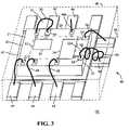
- FIG. 3shows an isometric view of integrated circuit 10 in a second alternate embodiment where bonding wire inductor 50 is attached between bonding pad 53 and lead 58 .
- FIG. 4is an isometric view of integrated circuit 10 in a third alternate embodiment showing bonding wire inductor 50 with axis 50 A located directly over line 54 intersecting the attachment points.
- semiconductor package 40has a higher profile, but the fabrication of this embodiment of inductor 50 may be easier in particular package configurations.
- FIG. 5shows a side view of integrated circuit 10 during a first stage in the fabrication of inductor 50 .
- a bonding wire 80is fed through a capillary 82 of a wire bonding tool.
- a shaper 86is fed through a conduit or tube 80 and positioned adjacent to semiconductor die 20 as shown.
- shaper 86 and tube 80are made of a low friction material such as Teflon®.
- Capillary 82is programmed to first attach wire 80 to bonding pad 51 and then feed wire 80 at a shallow angle toward shaper 86 , which is in its extended position in tube 84 . Capillary 82 then travels in a circular XY motion while moving more slowly in a Z-direction to wind bonding wire around shaper 86 one or more times to form coil 52 . The number of turns or windings is determined by the desired inductance of inductor 50 . Note that coil 52 is wound in a vertical or Z-direction with axis 50 A centered in shaper 86 .
- FIG. 5Ashows a side view of integrated circuit 10 during a second stage in the fabrication of inductor 50 .
- Capillary 82clamps bonding wire 80 while shaper 86 is moved to its retracted position in tube 84 , suspending coil 52 adjacent to semiconductor die 20 as shown.
- the low friction material used to form shaper 86 and tube 84facilitates the retraction of shaper 86 without deforming or disturbing coil 52 .
- FIG. 5Bis a side view of integrated circuit 10 during a third stage in the fabrication of inductor 50 . While clamping bonding wire 80 to prevent further wire feeding, capillary 82 is moved in X-direction to pull coil 52 into a horizontal position that extends over semiconductor die 20 . Bonding wire 80 is then attached to bonding pad 53 and severed to form inductor 50 as shown.
- inductor 50can be made in a similar fashion by attaching bonding wire to its first attachment point, winding it around shaper 86 to form coil 52 in a vertical direction and then pulling coil 52 into a horizontal position for bonding to its second attachment point.
- FIG. 6shows integrated circuit 10 at a selected manufacturing stage in an alternative method of forming inductor 50 .
- Bonding wire 80is heated and fed through threads 88 interior to capillary 82 .
- the threadsprecondition bonding wire 80 to a spring-like shape so that as bonding wire 80 emerges from capillary 82 and cools, it has the desired shape of coil 52 . Attachment then proceeds as previously described in conjunction with FIG. 5B .
- bonding wire 80preferably is doped with beryllium or a similar material to provide a springlike metal “memory” that retains the threaded shape.
- the present inventionprovides a structure and method of making a semiconductor device that includes one or more wire bond inductors housed in a semiconductor package along with a semiconductor die.
- the wire bond inductoris formed with a bonding wire attached to a top surface of a semiconductor die.
- the bonding wireis extended laterally a distance greater than a height of the bonding wire to define an insulating core of the inductor.
- the inductor formed in accordance with the inventionhas a high quality factor and a high frequency response while providing a low profile semiconductor package. While several methods of fabricating coils have been disclosed, it should be appreciated that other methods can provide a similar wire bond inductor.
- the inductorcan be made by utilizing a precoiled bonding wire that is doped with a material to retain its metal “memory”. The bonding wire is then fed through a wire bonding tool in such a way that it retains its shape during inductor formation. Hence, when a predetermined length of the precoiled bonding wire is fed through a capillary, the wire emerges from the capillary already having the shape of a coil.
Landscapes
- Engineering & Computer Science (AREA)
- Computer Hardware Design (AREA)
- Microelectronics & Electronic Packaging (AREA)
- Power Engineering (AREA)
- Physics & Mathematics (AREA)
- Condensed Matter Physics & Semiconductors (AREA)
- General Physics & Mathematics (AREA)
- Semiconductor Integrated Circuits (AREA)
Abstract
Description
Claims (18)
Priority Applications (1)
| Application Number | Priority Date | Filing Date | Title |
|---|---|---|---|
| US10/524,894US7227240B2 (en) | 2002-09-10 | 2002-09-10 | Semiconductor device with wire bond inductor and method |
Applications Claiming Priority (2)
| Application Number | Priority Date | Filing Date | Title |
|---|---|---|---|
| US10/524,894US7227240B2 (en) | 2002-09-10 | 2002-09-10 | Semiconductor device with wire bond inductor and method |
| PCT/US2002/028883WO2004025695A2 (en) | 2002-09-10 | 2002-09-10 | Semiconductor device with wire bond inductor and method |
Publications (2)
| Publication Number | Publication Date |
|---|---|
| US20050285262A1 US20050285262A1 (en) | 2005-12-29 |
| US7227240B2true US7227240B2 (en) | 2007-06-05 |
Family
ID=35504773
Family Applications (1)
| Application Number | Title | Priority Date | Filing Date |
|---|---|---|---|
| US10/524,894Expired - LifetimeUS7227240B2 (en) | 2002-09-10 | 2002-09-10 | Semiconductor device with wire bond inductor and method |
Country Status (1)
| Country | Link |
|---|---|
| US (1) | US7227240B2 (en) |
Cited By (24)
| Publication number | Priority date | Publication date | Assignee | Title |
|---|---|---|---|---|
| US20070128821A1 (en)* | 2005-12-05 | 2007-06-07 | Texas Instruments, Inc. | System and method for implementing transformer on package substrate |
| US20070139066A1 (en)* | 2005-12-19 | 2007-06-21 | Silicon Laboratories Inc. | Integrated current sensor package |
| US20070139032A1 (en)* | 2005-12-19 | 2007-06-21 | Silicon Laboratories Inc. | Integrated current sensor |
| US20070139835A1 (en)* | 2005-12-19 | 2007-06-21 | Alfano Donald E | Current sensor with reset circuit |
| US20080136399A1 (en)* | 2006-12-12 | 2008-06-12 | Alfano Donald E | Current sensor |
| US20080150102A1 (en)* | 2006-10-16 | 2008-06-26 | Fuji Electric Device Technology Co., Ltd. | Semiconductor device and manufacturing method of semiconductor device |
| US20090001962A1 (en)* | 2006-06-30 | 2009-01-01 | Dupuis Timothy J | Current sensor with reset circuit |
| US20090045520A1 (en)* | 2007-08-16 | 2009-02-19 | Aflash Technology Co., Ltd. | IC Device having Compact Design |
| US20090072388A1 (en)* | 2007-09-17 | 2009-03-19 | Infineon Technologies Ag | Semiconductor device with inductor |
| US20090168387A1 (en)* | 2007-12-31 | 2009-07-02 | Dirk Leipold | Packaged Integrated Circuits Having Inductors and Methods to Form Inductors in Packaged Integrated Circuits |
| US20090284248A1 (en)* | 2008-05-15 | 2009-11-19 | Etter Brett E | Method and apparatus for high current measurement |
| US20090321888A1 (en)* | 2007-12-06 | 2009-12-31 | Taiwan Semiconductor Manufacturing Company, Ltd. | Alignment for backside illumination sensor |
| US20100109140A1 (en)* | 2008-11-06 | 2010-05-06 | Oh Tac Keun | Flexible semiconductor package apparatus having a responsive bendable conductive wire member and a manufacturing the same |
| US20100124035A1 (en)* | 2008-11-20 | 2010-05-20 | International Business Machines Corporation | Integrating Capacitors Into Vias Of Printed Circuit Boards |
| US20110062549A1 (en)* | 2009-09-11 | 2011-03-17 | Stats Chippac, Ltd. | Semiconductor Device and Method of Forming Integrated Passive Device |
| US20110073359A1 (en)* | 2009-09-30 | 2011-03-31 | International Business Machines Corporation | Through-Hole-Vias In Multi-Layer Printed Circuit Boards |
| US20110108972A1 (en)* | 2009-11-12 | 2011-05-12 | International Business Machines Corporation | Integrated Circuit Die Stacks With Translationally Compatible Vias |
| US20110109381A1 (en)* | 2009-11-11 | 2011-05-12 | International Business Machines Corporation | Integrated Circuit Die Stacks With Rotationally Symmetric Vias |
| US20110110064A1 (en)* | 2009-11-12 | 2011-05-12 | International Business Machines Corporation | Integrating Circuit Die Stacks Having Initially Identical Dies Personalized With Fuses |
| US20110110065A1 (en)* | 2009-11-12 | 2011-05-12 | International Business Machines Corporation | Integrated Circuit Die Stacks Having Initially Identical Dies Personalized With Switches |
| US20110148543A1 (en)* | 2009-12-22 | 2011-06-23 | International Business Machines Corporation | Integrated Circuit With Inductive Bond Wires |
| US20130277849A1 (en)* | 2011-02-17 | 2013-10-24 | Fuji Electric Co., Ltd. | Internal wiring structure of semiconductor device |
| US20140266542A1 (en)* | 2013-03-15 | 2014-09-18 | Taiwan Semiconductor Manufacturing Company, Ltd. | Programmable Inductor |
| US20170338179A1 (en)* | 2016-05-20 | 2017-11-23 | Qualcomm Incorporated | Device package with wire bond assisted grounding and inductors |
Families Citing this family (50)
| Publication number | Priority date | Publication date | Assignee | Title |
|---|---|---|---|---|
| JP4137061B2 (en) | 2005-01-11 | 2008-08-20 | 株式会社カイジョー | Wire loop shape, semiconductor device having the wire loop shape, and wire bonding method |
| US20070296056A1 (en)* | 2006-06-27 | 2007-12-27 | Texas Instruments Incorporated | Integrated Circuits Having Controlled Inductances |
| US7524731B2 (en)* | 2006-09-29 | 2009-04-28 | Freescale Semiconductor, Inc. | Process of forming an electronic device including an inductor |
| US8389862B2 (en) | 2008-10-07 | 2013-03-05 | Mc10, Inc. | Extremely stretchable electronics |
| US8097926B2 (en) | 2008-10-07 | 2012-01-17 | Mc10, Inc. | Systems, methods, and devices having stretchable integrated circuitry for sensing and delivering therapy |
| US9123614B2 (en) | 2008-10-07 | 2015-09-01 | Mc10, Inc. | Methods and applications of non-planar imaging arrays |
| US8999807B2 (en) | 2010-05-27 | 2015-04-07 | Semiconductor Components Industries, Llc | Method for manufacturing a semiconductor component that includes a common mode choke and structure |
| US8766401B2 (en) | 2010-10-01 | 2014-07-01 | Semiconductor Components Industries, Llc | Method of manufacturing a semiconductor component and structure |
| US9159777B2 (en)* | 2011-04-15 | 2015-10-13 | Infineon Technologies Ag | Die arrangements containing an inductor coil and methods of manufacturing a die arrangement containing an inductor coil |
| US9065382B2 (en) | 2011-12-16 | 2015-06-23 | Skyworks Solutions, Inc. | Circuits and methods for increasing output frequency of an LC oscillator |
| US9226402B2 (en) | 2012-06-11 | 2015-12-29 | Mc10, Inc. | Strain isolation structures for stretchable electronics |
| US9295842B2 (en) | 2012-07-05 | 2016-03-29 | Mc10, Inc. | Catheter or guidewire device including flow sensing and use thereof |
| CN102790513B (en)* | 2012-07-30 | 2014-12-10 | 华为技术有限公司 | Power supply module and packaging method thereof |
| WO2014058473A1 (en) | 2012-10-09 | 2014-04-17 | Mc10, Inc. | Conformal electronics integrated with apparel |
| US9171794B2 (en) | 2012-10-09 | 2015-10-27 | Mc10, Inc. | Embedding thin chips in polymer |
| US9706647B2 (en) | 2013-05-14 | 2017-07-11 | Mc10, Inc. | Conformal electronics including nested serpentine interconnects |
| US9209132B2 (en) | 2013-07-26 | 2015-12-08 | Semiconductor Components Industries, Llc | Semiconductor component and method of manufacture |
| CA2920485A1 (en) | 2013-08-05 | 2015-02-12 | Mc10, Inc. | Flexible temperature sensor including conformable electronics |
| US9431385B2 (en) | 2013-08-09 | 2016-08-30 | Semiconductor Components Industries, Llc | Semiconductor component that includes a common mode filter and method of manufacturing the semiconductor component |
| US9111758B2 (en) | 2013-08-09 | 2015-08-18 | Semiconductor Components Industries, Llc | Semiconductor component and method of manufacture |
| KR20160065948A (en) | 2013-10-07 | 2016-06-09 | 엠씨10, 인크 | Conformal sensor systems for sensing and analysis |
| EP3071096A4 (en) | 2013-11-22 | 2017-08-09 | Mc10, Inc. | Conformal sensor systems for sensing and analysis of cardiac activity |
| US9692386B2 (en) | 2013-12-23 | 2017-06-27 | Qualcomm Incorporated | Three-dimensional wire bond inductor |
| CN105874606B (en) | 2014-01-06 | 2021-01-12 | Mc10股份有限公司 | Encapsulated conformal electronic systems and devices and methods of making and using the same |
| US10485118B2 (en) | 2014-03-04 | 2019-11-19 | Mc10, Inc. | Multi-part flexible encapsulation housing for electronic devices and methods of making the same |
| JP2017528908A (en)* | 2014-09-22 | 2017-09-28 | エムシー10 インコーポレイテッドMc10,Inc. | Method and apparatus for shaping and looping bonding wires that function as stretchable and bendable interconnects |
| USD781270S1 (en) | 2014-10-15 | 2017-03-14 | Mc10, Inc. | Electronic device having antenna |
| KR101905240B1 (en) | 2015-01-29 | 2018-10-05 | 앰코테크놀로지코리아(주) | Semiconductor package and manufacturing method thereof |
| WO2016134306A1 (en) | 2015-02-20 | 2016-08-25 | Mc10, Inc. | Automated detection and configuration of wearable devices based on on-body status, location, and/or orientation |
| US9831159B2 (en)* | 2015-06-09 | 2017-11-28 | Infineon Technologies Americas Corp. | Semiconductor package with embedded output inductor |
| WO2016209245A1 (en)* | 2015-06-25 | 2016-12-29 | Intel IP Corporation | Vertical inductor for wlcsp |
| WO2017015000A1 (en) | 2015-07-17 | 2017-01-26 | Mc10, Inc. | Conductive stiffener, method of making a conductive stiffener, and conductive adhesive and encapsulation layers |
| US10709384B2 (en) | 2015-08-19 | 2020-07-14 | Mc10, Inc. | Wearable heat flux devices and methods of use |
| EP4079383A3 (en) | 2015-10-01 | 2023-02-22 | Medidata Solutions, Inc. | Method and system for interacting with a virtual environment |
| US10532211B2 (en) | 2015-10-05 | 2020-01-14 | Mc10, Inc. | Method and system for neuromodulation and stimulation |
| US10181435B2 (en)* | 2015-11-02 | 2019-01-15 | Texas Instruments Incorporated | Lead frame assembly |
| US10332671B2 (en)* | 2015-11-08 | 2019-06-25 | Qualcomm Incorporated | Solenoid inductor |
| TWI619129B (en)* | 2015-12-15 | 2018-03-21 | 瑞昱半導體股份有限公司 | Inductor structure |
| US10673280B2 (en) | 2016-02-22 | 2020-06-02 | Mc10, Inc. | System, device, and method for coupled hub and sensor node on-body acquisition of sensor information |
| US10277386B2 (en) | 2016-02-22 | 2019-04-30 | Mc10, Inc. | System, devices, and method for on-body data and power transmission |
| CN109310340A (en) | 2016-04-19 | 2019-02-05 | Mc10股份有限公司 | Method and system for measuring sweat |
| US10447347B2 (en) | 2016-08-12 | 2019-10-15 | Mc10, Inc. | Wireless charger and high speed data off-loader |
| US10468073B2 (en) | 2017-12-29 | 2019-11-05 | Sandisk Technologies Llc | Transmission line optimization for multi-die systems |
| DE102019121894B4 (en) | 2019-08-14 | 2023-07-06 | Infineon Technologies Ag | Package with integrated multi-tap impedance structure and method for making such a package |
| CN112448561B (en)* | 2019-08-30 | 2022-04-15 | 台达电子企业管理(上海)有限公司 | Power module and preparation method thereof |
| GB2595680B (en)* | 2020-06-02 | 2023-05-31 | Heyday Integrated Circuits Sas | Galvanically isolated package for switch drive circuit with power transfer |
| US11302645B2 (en) | 2020-06-30 | 2022-04-12 | Western Digital Technologies, Inc. | Printed circuit board compensation structure for high bandwidth and high die-count memory stacks |
| US11456022B2 (en) | 2020-06-30 | 2022-09-27 | Western Digital Technologies, Inc. | Distributed grouped terminations for multiple memory integrated circuit systems |
| DE102020215346A1 (en) | 2020-12-04 | 2021-12-02 | Vitesco Technologies Germany Gmbh | Circuit arrangement |
| CN115513187B (en)* | 2022-11-23 | 2023-04-07 | 广东工业大学 | Chip of integrated on-chip inductor, integrated circuit and electronic device |
Citations (9)
| Publication number | Priority date | Publication date | Assignee | Title |
|---|---|---|---|---|
| JPH06140451A (en)* | 1992-10-27 | 1994-05-20 | Hitachi Ltd | Semiconductor integrated circuit device |
| JPH10289921A (en)* | 1997-04-14 | 1998-10-27 | Matsushita Electric Ind Co Ltd | Semiconductor device |
| WO2000010179A1 (en)* | 1998-08-14 | 2000-02-24 | Samsung Electronics Co., Ltd. | Bonding wire inductor and manufacturing method thereof |
| US6310393B1 (en)* | 1998-10-09 | 2001-10-30 | Matsushita Electric Industrial Co., Ltd. | Electric circuit and package for semiconductor |
| EP1202296A1 (en)* | 2000-10-27 | 2002-05-02 | Xerox Corporation | Out-of-plane microcoil using bonding wires and method for making |
| US20020118523A1 (en)* | 2001-02-23 | 2002-08-29 | Hitachi, Ltd. | Electronic circuit equipment using multilayer circuit board |
| US6512285B1 (en)* | 2001-10-05 | 2003-01-28 | Skyworks Solutions, Inc. | High inductance inductor in a semiconductor package |
| WO2004025695A2 (en)* | 2002-09-10 | 2004-03-25 | Semiconductor Components Industries L.L.C. | Semiconductor device with wire bond inductor and method |
| US6803665B1 (en)* | 2001-11-02 | 2004-10-12 | Skyworks Solutions, Inc. | Off-chip inductor |
- 2002
- 2002-09-10USUS10/524,894patent/US7227240B2/ennot_activeExpired - Lifetime
Patent Citations (10)
| Publication number | Priority date | Publication date | Assignee | Title |
|---|---|---|---|---|
| JPH06140451A (en)* | 1992-10-27 | 1994-05-20 | Hitachi Ltd | Semiconductor integrated circuit device |
| JPH10289921A (en)* | 1997-04-14 | 1998-10-27 | Matsushita Electric Ind Co Ltd | Semiconductor device |
| WO2000010179A1 (en)* | 1998-08-14 | 2000-02-24 | Samsung Electronics Co., Ltd. | Bonding wire inductor and manufacturing method thereof |
| US6775901B1 (en)* | 1998-08-14 | 2004-08-17 | Hai Young Lee | Bonding wire inductor |
| US6310393B1 (en)* | 1998-10-09 | 2001-10-30 | Matsushita Electric Industrial Co., Ltd. | Electric circuit and package for semiconductor |
| EP1202296A1 (en)* | 2000-10-27 | 2002-05-02 | Xerox Corporation | Out-of-plane microcoil using bonding wires and method for making |
| US20020118523A1 (en)* | 2001-02-23 | 2002-08-29 | Hitachi, Ltd. | Electronic circuit equipment using multilayer circuit board |
| US6512285B1 (en)* | 2001-10-05 | 2003-01-28 | Skyworks Solutions, Inc. | High inductance inductor in a semiconductor package |
| US6803665B1 (en)* | 2001-11-02 | 2004-10-12 | Skyworks Solutions, Inc. | Off-chip inductor |
| WO2004025695A2 (en)* | 2002-09-10 | 2004-03-25 | Semiconductor Components Industries L.L.C. | Semiconductor device with wire bond inductor and method |
Cited By (57)
| Publication number | Priority date | Publication date | Assignee | Title |
|---|---|---|---|---|
| US7453142B2 (en)* | 2005-12-05 | 2008-11-18 | Texas Instruments Incorporated | System and method for implementing transformer on package substrate |
| US20070128821A1 (en)* | 2005-12-05 | 2007-06-07 | Texas Instruments, Inc. | System and method for implementing transformer on package substrate |
| US7679162B2 (en)* | 2005-12-19 | 2010-03-16 | Silicon Laboratories Inc. | Integrated current sensor package |
| US20070139066A1 (en)* | 2005-12-19 | 2007-06-21 | Silicon Laboratories Inc. | Integrated current sensor package |
| US20070139032A1 (en)* | 2005-12-19 | 2007-06-21 | Silicon Laboratories Inc. | Integrated current sensor |
| US20070139835A1 (en)* | 2005-12-19 | 2007-06-21 | Alfano Donald E | Current sensor with reset circuit |
| US7362086B2 (en) | 2005-12-19 | 2008-04-22 | Silicon Laboratories Inc. | Integrated current sensor |
| US7397234B2 (en) | 2005-12-19 | 2008-07-08 | Silicon Laboratories Inc. | Current sensor with reset circuit |
| US7990132B2 (en) | 2006-06-30 | 2011-08-02 | Silicon Laboratories Inc. | Current sensor including an integrated circuit die including a first and second coil |
| US20090001962A1 (en)* | 2006-06-30 | 2009-01-01 | Dupuis Timothy J | Current sensor with reset circuit |
| US20080150102A1 (en)* | 2006-10-16 | 2008-06-26 | Fuji Electric Device Technology Co., Ltd. | Semiconductor device and manufacturing method of semiconductor device |
| US7705443B2 (en)* | 2006-10-16 | 2010-04-27 | Fuji Electric Device Technology Co., Ltd. | Semiconductor device with lead frame including conductor plates arranged three-dimensionally |
| US7821251B2 (en) | 2006-12-12 | 2010-10-26 | Silicon Laboratories Inc. | Current sensor |
| US20080136399A1 (en)* | 2006-12-12 | 2008-06-12 | Alfano Donald E | Current sensor |
| US20090045520A1 (en)* | 2007-08-16 | 2009-02-19 | Aflash Technology Co., Ltd. | IC Device having Compact Design |
| US7649747B2 (en)* | 2007-08-16 | 2010-01-19 | AFlash Technology Co., Ltd | IC device having compact design |
| US20090072388A1 (en)* | 2007-09-17 | 2009-03-19 | Infineon Technologies Ag | Semiconductor device with inductor |
| US7986023B2 (en)* | 2007-09-17 | 2011-07-26 | Infineon Technologies Ag | Semiconductor device with inductor |
| US8558351B2 (en) | 2007-12-06 | 2013-10-15 | Taiwan Semiconductor Manufacturing Company, Ltd. | Alignment for backside illumination sensor |
| US20090321888A1 (en)* | 2007-12-06 | 2009-12-31 | Taiwan Semiconductor Manufacturing Company, Ltd. | Alignment for backside illumination sensor |
| US8227899B2 (en)* | 2007-12-06 | 2012-07-24 | Taiwan Semiconductor Manufacturing Company, Ltd. | Alignment for backside illumination sensor |
| US8900966B2 (en) | 2007-12-06 | 2014-12-02 | Taiwan Semiconductor Manufacturing Company, Ltd. | Alignment for backside illumination sensor |
| US8389868B2 (en)* | 2007-12-31 | 2013-03-05 | Texas Instruments Incorporated | Packaged integrated circuits having inductors and methods to form inductors in packaged integrated circuits |
| US20090168387A1 (en)* | 2007-12-31 | 2009-07-02 | Dirk Leipold | Packaged Integrated Circuits Having Inductors and Methods to Form Inductors in Packaged Integrated Circuits |
| US7728578B2 (en) | 2008-05-15 | 2010-06-01 | Silicon Laboratories Inc. | Method and apparatus for high current measurement |
| US20090284248A1 (en)* | 2008-05-15 | 2009-11-19 | Etter Brett E | Method and apparatus for high current measurement |
| US8618656B2 (en) | 2008-11-06 | 2013-12-31 | Hynix Semiconductor Inc. | Flexible semiconductor package apparatus having a responsive bendable conductive wire member and a manufacturing the same |
| US8049332B2 (en)* | 2008-11-06 | 2011-11-01 | Hynix Semiconductor Inc. | Flexible semiconductor package apparatus having a responsive bendable conductive wire member and a manufacturing the same |
| US20100109140A1 (en)* | 2008-11-06 | 2010-05-06 | Oh Tac Keun | Flexible semiconductor package apparatus having a responsive bendable conductive wire member and a manufacturing the same |
| US8107254B2 (en) | 2008-11-20 | 2012-01-31 | International Business Machines Corporation | Integrating capacitors into vias of printed circuit boards |
| US20100124035A1 (en)* | 2008-11-20 | 2010-05-20 | International Business Machines Corporation | Integrating Capacitors Into Vias Of Printed Circuit Boards |
| US8513812B2 (en) | 2009-09-11 | 2013-08-20 | Stats Chippac, Ltd. | Semiconductor device and method of forming integrated passive device |
| US8164158B2 (en)* | 2009-09-11 | 2012-04-24 | Stats Chippac, Ltd. | Semiconductor device and method of forming integrated passive device |
| US20110062549A1 (en)* | 2009-09-11 | 2011-03-17 | Stats Chippac, Ltd. | Semiconductor Device and Method of Forming Integrated Passive Device |
| US9277653B2 (en) | 2009-09-30 | 2016-03-01 | Lenovo Enterprise Solutions (Singapore) Pte. Ltd. | Through-hole-vias in multi-layer printed circuit boards |
| US8242384B2 (en) | 2009-09-30 | 2012-08-14 | International Business Machines Corporation | Through hole-vias in multi-layer printed circuit boards |
| US20110073359A1 (en)* | 2009-09-30 | 2011-03-31 | International Business Machines Corporation | Through-Hole-Vias In Multi-Layer Printed Circuit Boards |
| US8432027B2 (en) | 2009-11-11 | 2013-04-30 | International Business Machines Corporation | Integrated circuit die stacks with rotationally symmetric vias |
| US20110109381A1 (en)* | 2009-11-11 | 2011-05-12 | International Business Machines Corporation | Integrated Circuit Die Stacks With Rotationally Symmetric Vias |
| US8315068B2 (en) | 2009-11-12 | 2012-11-20 | International Business Machines Corporation | Integrated circuit die stacks having initially identical dies personalized with fuses and methods of manufacturing the same |
| US8258619B2 (en) | 2009-11-12 | 2012-09-04 | International Business Machines Corporation | Integrated circuit die stacks with translationally compatible vias |
| US20110110064A1 (en)* | 2009-11-12 | 2011-05-12 | International Business Machines Corporation | Integrating Circuit Die Stacks Having Initially Identical Dies Personalized With Fuses |
| US20110108972A1 (en)* | 2009-11-12 | 2011-05-12 | International Business Machines Corporation | Integrated Circuit Die Stacks With Translationally Compatible Vias |
| US20110110065A1 (en)* | 2009-11-12 | 2011-05-12 | International Business Machines Corporation | Integrated Circuit Die Stacks Having Initially Identical Dies Personalized With Switches |
| US8310841B2 (en) | 2009-11-12 | 2012-11-13 | International Business Machines Corporation | Integrated circuit die stacks having initially identical dies personalized with switches and methods of making the same |
| US9076770B2 (en) | 2009-11-12 | 2015-07-07 | Lenovo Enterprise Solutions (Singapore) Pte. Ltd. | Integrated circuit die stacks having initially identical dies personalized with fuses and methods of manufacturing the same |
| US8780578B2 (en) | 2009-11-12 | 2014-07-15 | International Business Machines Corporation | Integrated circuit die stacks having initially identical dies personalized with switches |
| US8823162B2 (en) | 2009-11-12 | 2014-09-02 | International Business Machines Corporation | Integrated circuit die stacks with translationally compatible vias |
| US9646947B2 (en) | 2009-12-22 | 2017-05-09 | Lenovo Enterprise Solutions (Singapore) Pte. Ltd. | Integrated circuit with inductive bond wires |
| US20110148543A1 (en)* | 2009-12-22 | 2011-06-23 | International Business Machines Corporation | Integrated Circuit With Inductive Bond Wires |
| US8710674B2 (en)* | 2011-02-17 | 2014-04-29 | Fuji Electric Co., Ltd. | Internal wiring structure of semiconductor device |
| US20130277849A1 (en)* | 2011-02-17 | 2013-10-24 | Fuji Electric Co., Ltd. | Internal wiring structure of semiconductor device |
| US20140266542A1 (en)* | 2013-03-15 | 2014-09-18 | Taiwan Semiconductor Manufacturing Company, Ltd. | Programmable Inductor |
| US10269489B2 (en)* | 2013-03-15 | 2019-04-23 | Taiwan Semiconductor Manufacturing Company, Ltd. | Programmable inductor |
| US11756731B2 (en) | 2013-03-15 | 2023-09-12 | Taiwan Semiconductor Manufacturing Company, Ltd. | Programmable inductor |
| US12243681B2 (en) | 2013-03-15 | 2025-03-04 | Taiwan Semiconductor Manufacturing Company, Ltd. | Programmable inductor and methods of manufacture |
| US20170338179A1 (en)* | 2016-05-20 | 2017-11-23 | Qualcomm Incorporated | Device package with wire bond assisted grounding and inductors |
Also Published As
| Publication number | Publication date |
|---|---|
| US20050285262A1 (en) | 2005-12-29 |
Similar Documents
| Publication | Publication Date | Title |
|---|---|---|
| US7227240B2 (en) | Semiconductor device with wire bond inductor and method | |
| WO2004025695A2 (en) | Semiconductor device with wire bond inductor and method | |
| US4860433A (en) | Method of manufacturing an inductance element | |
| US20050122198A1 (en) | Inductive device including bond wires | |
| KR100954464B1 (en) | Leadframe inductors | |
| US5872403A (en) | Package for a power semiconductor die and power supply employing the same | |
| TW200950013A (en) | Quad flat non-lead semiconductor package and method for making quad flat non-lead semiconductor package | |
| US20190164872A1 (en) | Electronic device | |
| WO2010105157A2 (en) | Microelectronic assembly with impedance controlled wirebond and conductive reference element | |
| US6465896B1 (en) | Coils integrated in IC-package | |
| US20220351901A1 (en) | Low Cost In-Package Power Inductor | |
| US20250316416A1 (en) | Molded inductor with magnetic core having mold flow enhancing channels | |
| US12148556B2 (en) | Integrated magnetic assembly | |
| CN114256213A (en) | Electronic package and manufacturing method thereof | |
| US6803665B1 (en) | Off-chip inductor | |
| US20060125079A1 (en) | High density package interconnect wire bond strip line and method therefor | |
| HK1081326B (en) | Semiconductor device with wire bond inductor and method | |
| US20230005874A1 (en) | Semiconductor device packages with high angle wire bonding and non-gold bond wires | |
| CN115799228A (en) | Integrated module and method for producing same | |
| US20250111985A1 (en) | Lead structure for an inductive coil | |
| US12191252B2 (en) | Semiconductor fuse with multi-bond wire | |
| US20240387102A1 (en) | Inductor module and manufacturing method thereof | |
| CN107507780B (en) | Semiconductor packaging method and semiconductor structure | |
| CN115547623A (en) | Conical inductor packaging structure and preparation method thereof | |
| CN113474860A (en) | Isolation transformer with integrated shielding topology for reduced EMI |
Legal Events
| Date | Code | Title | Description |
|---|---|---|---|
| AS | Assignment | Owner name:SEMICONDUCTOR COMPONENTS INDUSTRIES, L.L.C. OF, AR Free format text:ASSIGNMENT OF ASSIGNORS INTEREST;ASSIGNORS:KNAPP, JAMES;CARNEY, FRANCIS;ANDERSON, HAROLD;AND OTHERS;REEL/FRAME:016920/0329;SIGNING DATES FROM 20040910 TO 20040924 | |
| STCF | Information on status: patent grant | Free format text:PATENTED CASE | |
| AS | Assignment | Owner name:JPMORGAN CHASE BANK, N.A., NEW YORK Free format text:SECURITY AGREEMENT;ASSIGNOR:SEMICONDUCTOR COMPONENTS INDUSTRIES, LLC;REEL/FRAME:019795/0808 Effective date:20070906 Owner name:JPMORGAN CHASE BANK, N.A.,NEW YORK Free format text:SECURITY AGREEMENT;ASSIGNOR:SEMICONDUCTOR COMPONENTS INDUSTRIES, LLC;REEL/FRAME:019795/0808 Effective date:20070906 | |
| FPAY | Fee payment | Year of fee payment:4 | |
| AS | Assignment | Owner name:SEMICONDUCTOR COMPONENTS INDUSTRIES, LLC, ARIZONA Free format text:RELEASE OF SECURITY INTEREST;ASSIGNOR:JPMORGAN CHASE BANK, N.A.;REEL/FRAME:033686/0092 Effective date:20100511 | |
| FPAY | Fee payment | Year of fee payment:8 | |
| AS | Assignment | Owner name:DEUTSCHE BANK AG NEW YORK BRANCH, NEW YORK Free format text:SECURITY INTEREST;ASSIGNOR:SEMICONDUCTOR COMPONENTS INDUSTRIES, LLC;REEL/FRAME:038620/0087 Effective date:20160415 | |
| AS | Assignment | Owner name:DEUTSCHE BANK AG NEW YORK BRANCH, AS COLLATERAL AGENT, NEW YORK Free format text:CORRECTIVE ASSIGNMENT TO CORRECT THE INCORRECT PATENT NUMBER 5859768 AND TO RECITE COLLATERAL AGENT ROLE OF RECEIVING PARTY IN THE SECURITY INTEREST PREVIOUSLY RECORDED ON REEL 038620 FRAME 0087. ASSIGNOR(S) HEREBY CONFIRMS THE SECURITY INTEREST;ASSIGNOR:SEMICONDUCTOR COMPONENTS INDUSTRIES, LLC;REEL/FRAME:039853/0001 Effective date:20160415 Owner name:DEUTSCHE BANK AG NEW YORK BRANCH, AS COLLATERAL AG Free format text:CORRECTIVE ASSIGNMENT TO CORRECT THE INCORRECT PATENT NUMBER 5859768 AND TO RECITE COLLATERAL AGENT ROLE OF RECEIVING PARTY IN THE SECURITY INTEREST PREVIOUSLY RECORDED ON REEL 038620 FRAME 0087. ASSIGNOR(S) HEREBY CONFIRMS THE SECURITY INTEREST;ASSIGNOR:SEMICONDUCTOR COMPONENTS INDUSTRIES, LLC;REEL/FRAME:039853/0001 Effective date:20160415 | |
| MAFP | Maintenance fee payment | Free format text:PAYMENT OF MAINTENANCE FEE, 12TH YEAR, LARGE ENTITY (ORIGINAL EVENT CODE: M1553); ENTITY STATUS OF PATENT OWNER: LARGE ENTITY Year of fee payment:12 | |
| AS | Assignment | Owner name:FAIRCHILD SEMICONDUCTOR CORPORATION, ARIZONA Free format text:RELEASE OF SECURITY INTEREST IN PATENTS RECORDED AT REEL 038620, FRAME 0087;ASSIGNOR:DEUTSCHE BANK AG NEW YORK BRANCH, AS COLLATERAL AGENT;REEL/FRAME:064070/0001 Effective date:20230622 Owner name:SEMICONDUCTOR COMPONENTS INDUSTRIES, LLC, ARIZONA Free format text:RELEASE OF SECURITY INTEREST IN PATENTS RECORDED AT REEL 038620, FRAME 0087;ASSIGNOR:DEUTSCHE BANK AG NEW YORK BRANCH, AS COLLATERAL AGENT;REEL/FRAME:064070/0001 Effective date:20230622 |