US7225047B2 - Method, system and medium for controlling semiconductor wafer processes using critical dimension measurements - Google Patents
Method, system and medium for controlling semiconductor wafer processes using critical dimension measurementsDownload PDFInfo
- Publication number
- US7225047B2 US7225047B2US10/100,184US10018402AUS7225047B2US 7225047 B2US7225047 B2US 7225047B2US 10018402 AUS10018402 AUS 10018402AUS 7225047 B2US7225047 B2US 7225047B2
- Authority
- US
- United States
- Prior art keywords
- implant
- annealing
- tool
- wafers
- dimension
- Prior art date
- Legal status (The legal status is an assumption and is not a legal conclusion. Google has not performed a legal analysis and makes no representation as to the accuracy of the status listed.)
- Expired - Lifetime
Links
- 238000000034methodMethods0.000titleclaimsabstractdescription185
- 230000008569processEffects0.000titleclaimsabstractdescription154
- 239000004065semiconductorSubstances0.000titleclaimsabstractdescription14
- 238000005259measurementMethods0.000titleclaimsdescription15
- 235000012431wafersNutrition0.000claimsabstractdescription106
- 238000000137annealingMethods0.000claimsabstractdescription101
- 238000012545processingMethods0.000claimsabstractdescription88
- 238000004519manufacturing processMethods0.000claimsabstractdescription14
- 239000007943implantSubstances0.000claimsdescription65
- 125000001475halogen functional groupChemical group0.000claimsdescription31
- 150000002500ionsChemical class0.000claimsdescription10
- 238000012360testing methodMethods0.000description10
- 230000007246mechanismEffects0.000description9
- 238000010586diagramMethods0.000description7
- 238000004377microelectronicMethods0.000description7
- 238000012937correctionMethods0.000description6
- 238000004891communicationMethods0.000description5
- 238000004088simulationMethods0.000description5
- 239000002609mediumSubstances0.000description4
- 238000005516engineering processMethods0.000description3
- 230000006870functionEffects0.000description3
- 238000012986modificationMethods0.000description3
- 230000004048modificationEffects0.000description3
- 229920002120photoresistant polymerPolymers0.000description3
- 230000000694effectsEffects0.000description2
- 238000005530etchingMethods0.000description2
- 238000002474experimental methodMethods0.000description2
- 239000000463materialSubstances0.000description2
- 238000009448modified atmosphere packagingMethods0.000description2
- 238000012544monitoring processMethods0.000description2
- 235000019837monoammonium phosphateNutrition0.000description2
- 230000003287optical effectEffects0.000description2
- 238000003860storageMethods0.000description2
- ZOXJGFHDIHLPTG-UHFFFAOYSA-NBoronChemical compound[B]ZOXJGFHDIHLPTG-UHFFFAOYSA-N0.000description1
- 206010057362UnderdoseDiseases0.000description1
- 229910052785arsenicInorganic materials0.000description1
- RQNWIZPPADIBDY-UHFFFAOYSA-Narsenic atomChemical compound[As]RQNWIZPPADIBDY-UHFFFAOYSA-N0.000description1
- 230000015572biosynthetic processEffects0.000description1
- 229910052796boronInorganic materials0.000description1
- 238000004364calculation methodMethods0.000description1
- 230000008859changeEffects0.000description1
- 238000004590computer programMethods0.000description1
- 238000005094computer simulationMethods0.000description1
- 239000004020conductorSubstances0.000description1
- 238000010276constructionMethods0.000description1
- 238000013461designMethods0.000description1
- 238000007689inspectionMethods0.000description1
- 230000010354integrationEffects0.000description1
- 238000010884ion-beam techniqueMethods0.000description1
- 238000001459lithographyMethods0.000description1
- 239000013307optical fiberSubstances0.000description1
- 230000002093peripheral effectEffects0.000description1
- 238000000206photolithographyMethods0.000description1
- 229910021420polycrystalline siliconInorganic materials0.000description1
- 229920005591polysiliconPolymers0.000description1
- 238000012805post-processingMethods0.000description1
- 238000004886process controlMethods0.000description1
- 230000008054signal transmissionEffects0.000description1
- 239000007787solidSubstances0.000description1
- 241000894007speciesSpecies0.000description1
- 239000006163transport mediaSubstances0.000description1
- 230000000007visual effectEffects0.000description1
Images


Classifications
- H—ELECTRICITY
- H01—ELECTRIC ELEMENTS
- H01L—SEMICONDUCTOR DEVICES NOT COVERED BY CLASS H10
- H01L21/00—Processes or apparatus adapted for the manufacture or treatment of semiconductor or solid state devices or of parts thereof
- H01L21/67—Apparatus specially adapted for handling semiconductor or electric solid state devices during manufacture or treatment thereof; Apparatus specially adapted for handling wafers during manufacture or treatment of semiconductor or electric solid state devices or components ; Apparatus not specifically provided for elsewhere
- H01L21/67005—Apparatus not specifically provided for elsewhere
- H01L21/67242—Apparatus for monitoring, sorting or marking
- H01L21/67253—Process monitoring, e.g. flow or thickness monitoring
- H—ELECTRICITY
- H01—ELECTRIC ELEMENTS
- H01L—SEMICONDUCTOR DEVICES NOT COVERED BY CLASS H10
- H01L21/00—Processes or apparatus adapted for the manufacture or treatment of semiconductor or solid state devices or of parts thereof
- H—ELECTRICITY
- H01—ELECTRIC ELEMENTS
- H01L—SEMICONDUCTOR DEVICES NOT COVERED BY CLASS H10
- H01L22/00—Testing or measuring during manufacture or treatment; Reliability measurements, i.e. testing of parts without further processing to modify the parts as such; Structural arrangements therefor
- H—ELECTRICITY
- H01—ELECTRIC ELEMENTS
- H01L—SEMICONDUCTOR DEVICES NOT COVERED BY CLASS H10
- H01L22/00—Testing or measuring during manufacture or treatment; Reliability measurements, i.e. testing of parts without further processing to modify the parts as such; Structural arrangements therefor
- H01L22/20—Sequence of activities consisting of a plurality of measurements, corrections, marking or sorting steps
Definitions
- the present inventionrelates to methods, systems and mediums for controlling processes for manufacturing micro-electronic devices based on, in part, one or more measurements made on one or more critical dimensions such as gate lengths of devices.
- the measured critical dimensionscan be used in determining parameter values in, for example, feed-forward and/or feed-back controlling mechanisms to reduce variations on the critical dimensions.
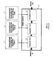
- FIG. 1illustrates a conventional semiconductor process module 101 that performs one or more processes for fabricating micro-electronic devices on a batch of wafers.
- a conventional process moduleincludes a set of processing tools (e.g., an implanter tool 1 105 , an implanter tool 2 107 and an annealing tool 109 ) and a controller for each tool 111 , 112 , 113 .
- the conventional controllers 111 , 112 , 113are configured to operate/control their respective processing tools using baseline parameter values (e.g., process conditions).
- the baseline parameter valuesdefine, for example, implant (e.g., a doping level) and anneal (e.g., a peak temperature) conditions for the implanter tools and annealing tool, respectively.
- the baseline parameter valuesare not adjusted for processing one wafer to another wafer.
- the conventional controllers 111 , 112 , 113once they begin to use a certain set of baseline parameter values, apply the same baseline parameter values to all wafers in a batch.
- the baseline parameter valuescannot be adjusted even when undesirable variations are detected. These variations can be caused by a previous processing step or by any of the tool 105 , 107 , 109 .
- Embodiments of the present inventionadvantageously overcome the above described shortcomings of conventional processing modules.
- embodiments of the present inventionprovide systems, methods and mediums for controlling processes for fabricating micro-electronic devices using critical dimension measurements.
- at least some embodiments of the present inventioninclude a method of processing a number of wafers for manufacturing semiconductor devices. The method comprises the steps of measuring at least one dimension (e.g., gate length) of at least one of the devices being fabricated on at least one of the wafers and determining control parameter values (also referred to as process conditions) based on the at least one measured dimension.
- at least one dimensione.g., gate length
- control parameter valuesalso referred to as process conditions
- the methodmay also include the step of controlling at least one semiconductor manufacturing tool to process the at least one of the wafers based on the parameter values (e.g., in a feed-forward/feed-back manner).
- the at least one processing toolcan include at least one implanter tool.
- FIG. 1is a drawing illustrating a conventional controller and processing tools
- FIG. 2is a graph illustrating relationships between variations of gate lengths of devices and percent in deviation of performance of produced devices
- FIGS. 3A and 3Bare block diagrams showing first example embodiments of the present invention.
- FIG. 4is a schematic drawing illustrating an under etch condition and corrections thereof as contemplated by at least some embodiments of the present invention
- FIG. 5is a block diagram/flowchart illustrating relationships between a module controller and a module/tool monitor as contemplated by at least some embodiments of the present invention
- FIG. 6is a flowchart illustrating example steps performed by the first example embodiment of the present invention.
- FIG. 7is a block diagram illustrating a second example embodiment of the present invention.
- FIG. 8is a flowchart illustrating example steps performed by the second example embodiment of the present invention.
- FIG. 9is a block diagram illustrating a third example embodiment of the present invention.
- FIGS. 10 a and 10 bare flowcharts illustrating example steps performed by the third example embodiment of the present invention.
- FIG. 11is a table illustrating improvements introduced by the corrections of the present invention.
- FIG. 12is a graph illustrating changes introduced by a compensated SDE dosage
- FIG. 13is a block diagram representation of an example embodiment of a module controller.
- FIG. 14illustrates one example of a memory medium which may be used for storing computer programs of the module controller of the present invention.
- the undesirable variations mentioned abovecan be compensated for by first measuring a critical dimension of a device being processed.
- a critical dimension (CD)is a dimension of a particular location of a device (e.g., a gate length). Variations in the CD may cause undesirable performance variations on the device. If such variations in a CD are detected, a subsequent processing tool(s) may be adjusted such that the undesirable variation is alleviated. This is done by generating one or more parameter values based upon the amount of the variation. The parameter values are then used by the processing tool(s) to make the appropriate adjustment.
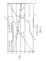
- FIG. 2shows a graph 201 illustrating deviations in device performances caused by variations in CDs of devices. More specifically, FIG. 2 illustrates deviations in a number of parameters that measure performances of produced micro-electronic devices (e.g., microprocessors) having a target for the CD as 130 nm.
- the parametersinclude: d Tau, d I off , d I DSAT and d V T (“d” represents change/deviation).
- d Tauis deviation in gate delay time, which is defined as C*V dd /I DSAT (C: capacitance; Vdd: drain voltage; and I DSAT saturation current), the value of d I off is deviation in leakage current; the value of d I DSAT is deviation in saturation drive current; and the value of d V T is deviation in threshold voltage.
- Ccapacitance
- Vdddrain voltage
- I DSAT saturation currentthe value of d I off is deviation in leakage current
- d I DSATis deviation in saturation drive current
- the value of d V Tis deviation in threshold voltage.
- variations in the CDhave a significant impact on device performances.
- a 10 nm variation (from 130 nm to 140 nm) in the CDis shown as resulting in about a 16% variation in Tau and more than a 30% variation in leakage current (I off ). Both Tau and I off are critical as they affect device speed and battery life, respectively.
- the conventional processing modules and their process toolsare incapable of correcting undesirable variations because, in part, they are not configured to measure CDs and/or use the CD measurements generating/adjusting parameter values.
- FIGS. 3A–B , 7 and 9At least some embodiments of the present invention are shown in FIGS. 3A–B , 7 and 9 . More specifically, in FIG. 3A–B , an example module controller 305 that receives CD measurements of one or more devices on a wafer and generates parameter values based thereon is illustrated. In FIG. 7 , another example module controller 705 is illustrated wherein the module controller 705 receives CD and junction depth measurements and generates parameter values based thereon. FIG. 9 illustrates yet another example module controller 905 , wherein the module controller 905 includes metrology tools for checking dosages. These embodiments are provided only as examples, and various individual components, devices and/or tools of one embodiment can be omitted, added to, and/or combined with other embodiments. Detailed descriptions of these embodiments and other aspects of the present invention are provided below.
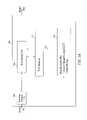
- FIG. 3Athis figure illustrates an example embodiment process module 301 of the present invention in which critical dimension (CD) measurements are made and the measured CD values are used in controlling one or more processing tools by generating/adjusting parameter values.
- the example embodiment of FIG. 3Aalso includes a metrology tool 303 , a module controller 305 , a tool monitor 313 and a process tool 308 .
- FIG. 3Billustrates a somewhat more specific example embodiment depicting similar concepts. More specifically, the example embodiment depicted in FIG. 3B further includes processing tools 307 , 309 , 311 .
- the metrology tool 303is configured to measure CDs of one or more devices being fabricated on wafers.
- a CDis, for example, gate lengths of devices.
- CDs of devices on all dies of a waferare measured. The average of the measured CDs is calculated and then communicated to the module controller 305 .
- CD measurementsare made on a sub-set of dies and their average is calculated and communicated to the module controller 305 .
- the sub-set of diescan be a line of dies on a wafer (e.g., a horizontal line, a vertical line or a line of any orientation), a portion of dies on a wafer (e.g., an upper half or an upper left quadrant), any random combination of dies or any one die.
- gate lengthis a CD often mentioned herein only by way of example, and that embodiments of the present invention contemplate that a CD can also be any facet or dimension on a device that may cause performance variations in produced devices when it varies from a target by a certain amount.
- the set of process tools in FIG. 3Bcan include one or any combination of processing tools such as an implanter tool 1 307 , an implanter tool 2 309 and an annealing tool 311 .
- the tool 308 of FIG. 3Acan be any one of an implanter tool or an annealing tool.
- the number of processing tools and their typesare not limited to only having, for example, two implanter tools and one annealing tool as shown in FIG. 3B .
- the various combinations of implanter and annealing toolsdo not necessarily represent all the tools that may be required to process a wafer.
- Other tools that can be includedare, for example, photolithography tools, etchers, cleaners, etc.
- the implanter and annealing toolsare illustrated as example tools that can be controlled by the module controller 305 .
- the process toolsregardless which one of the above-described embodiments is used, are configured to provide various implant process(es), anneal process(es) and/or other process(es) by the module controller 305 and tool monitor 313 .
- the tool monitor 313would be unnecessary, and that, e.g., at least some of the functions provided by the tool monitor 313 can be controlled by the module controller 305 and/or a processing tool, itself.
- Embodiments of the present inventioncan be configured to include any type of implanter tools and annealing tools that can be controlled by using, in part, parameters and specific values thereof.
- implant and annealing toolssuch as single wafer and batch tools that include: low energy, high current, medium current, high energy implanters, batch furnace, single RTP annealers, beamline and/or plasma based doping tools.
- the implanter tool 1 307is configured to perform source drain contracts and SDE implants.
- the implanter tool 2 309is configured to perform halo/V T /Well implants.
- the implanter tools 1 and 2can be QuantumTM and SwiftTM, respectively, both of which are manufactured by Applied Materials, Inc. of Santa Clara, Calif.
- An example the annealing tool 311is RadianceTM, manufactured by Applied Materials, Inc. of Santa Clara, Calif. These process tools are provided herein only as examples. Other types of implanter and annealing tools that can thus also be used in embodiments of the present invention.
- each processing toolmay be coupled to a tool controller 502 (shown in FIG. 5 ) configured to control its respective process control and set-up based on information (e.g., process conditions) received from the module controller 305 .
- the process toolse.g., the implanter tools 1 and 2 and the annealing tool
- their tool controllersare coupled to the module controller 305 .
- the module controller 305is configured to operate/control the implanter tools 1 and 2 and the annealing tool 311 using parameter values. In particular, based on CD measurements, the module controller 305 determines appropriate values for parameter values.
- parametersexamples include a halo angle, a dose and energy level, a Source-Drain-Extension (SDE) dose level, an energy and tilt level, a pocket implant dose level, a channel and channel V T adjust implant dose level, an energy and tilt level, a Rapid Thermal Processing (RTP) peak temperature level, and/or anneal time length.
- SDESource-Drain-Extension
- RTPRapid Thermal Processing
- the critical dimensionis measured by the metrology tool 303 .
- the measured CDcan be different from a target CD (thus, possibly indicating the existence of an undesirable variation).
- a devicemay have been erroneously processed such that a measured CD (in this example, gate length) 403 is wider than a target 401 , which may have been caused by a photoresist layer 405 that has been underetched in a previous processing step.
- the wider gate length 403in turn can introduce undesirable variation into other aspects of devices such as effective channel length (e.g., it may cause a wider effective channel length 412 ).
- the effective channel lengthwould have met a target effective channel length 411 .
- the wider gate length 403the measured effective channel length is wider than the target effective channel length.
- embodiments of the present inventioncan compensate for this undesirable variation by determining parameter values (based on the gate length) and using them to modify the operation of one or more processing tools to form final effective channel length to be substantially identical/similar to the target effective channel length.
- the module controller 305includes a technique for determining parameter values based on measured CD values.
- the parameter valuescan then be stored in an active channel control lookup table (LUT).
- the parameter values for the LUTare created, for example, by using a computer implemented simulation package (e.g., T CAD, manufactured by Integrated System Engineering, ISE, of Switzerland).
- the simulation packagecan be configured to generate (e.g., calculate) values of parameters for a particular CD measurement.
- the simulation packageis configured to generate values of parameters (e.g., SDE, halo and RTP process conditions) for a particular gate length measurement in order to compensate for any CD variations (e.g., an over or under etching).
- parameterse.g., SDE, halo and RTP process conditions
- an array of values of SDE, halo and RTP conditionsare created for a series of gate lengths at a predetermined interval (e.g., every 0.1 nm, 1 nm or multiple nms of gate lengths).
- the array of parameter values along with their corresponding measured CD valuesis then collected into the LUT, which is then used to lookup a corresponding set of parameter values for any measured gate length.
- An example of the LUTis shown below in Table 1.
- E (keV),” “Dose,” “tilt/twist,” “peak temperature” and “up/cooldown rate”are example parameters and the entries of the table are example parameter values.
- the LUT created using the simulation packageis refined based on empirical data collected by performing experiments.
- a set of test wafersis fabricated to form devices having different average gate lengths.
- the test wafersare then put through the processes by the implanter tools 1 and 2 and annealing tool (e.g., the tools illustrated in FIG. 3B ) using the parameter values of the LUT by the module controller for that particular measured CD.
- the resultsare collected and compared against predicted results by the simulation package. If the test wafers are processed to produce devices with the predicted results, then no adjustment on the parameter values is made to the LUT. If not, then the LUT entry is replaced or adjusted in accordance with the data collected during the experiments.
- a number of LUTscan be created, each of which may relate to device types and/or technology nodes.
- Device typescan be microprocessors, memory chips, programmable ROMs, etc.
- a technology nodecan be a 100 nm node, a 130 nm node, a 180 nm node, etc.
- a LUTcan also be created using only experimental data without using a computer simulation package.
- one or more equationsare derived to determine the parameter values for measured CDs.
- a graphical representationmay be used in determining the parameter values for measured CDs. It should be noted that the present invention can use a LUT, one or more equations, one or more graphical representations, or other mechanisms for determining parameter values.
- FIG. 5is a block diagram illustrating some example operations of the module controller 305 and tool monitor 313 .
- the module controller 305can be configured to include an active channel control LUT.
- the module controller 305can also (or alternatively) use an external LUT to receive or determine parameter values (step 501 ).
- the module controller 305uses the parameter values of “SDE implant” from the LUT to control the implanter tool 1 (step 503 ) and uses the parameter values of “halo implant” from the LUT to control the implanter tool 2 (step 505 ).
- the module controller 305uses the parameter values of RTP from the LUT to control the annealing tool (step 507 ). As indicated previously, steps such as those can be used to compensate an undesirable variance within devices on a wafer caused by some previous process step (e.g., lithography, photoresist and/or etching process steps) performed by a previous manufacturing tool. Consequently, these mechanisms of controlling the process tools based on parameter values from the LUT are referred to as feed-forward control mechanisms.
- the tool monitor 313is configured to monitor activities of each process tool (step 509 ).
- the module controller 305can also be configured to adjust parameter values and setups of the process tools based on the results of the monitoring step 509 by the tool monitor (step 511 ).
- setups of the process toolscan be one or any combination of a beam-current, a vacuum pressure, tool pressure, tool temperature, etc.
- the feed-forward control mechanism of the module controller 305uses three parameter values (i.e., SDE, halo and RTP conditions) to operate/control three process tools.
- SDEis used to control the implanter tool 1
- halois used to control implanter 2
- RTPis used in controlling the annealing tool.
- not all parameter valuesmay be required.
- only the SDE parametermay be determined by using the LUT and only implanter tool 1 is controlled by the feed-forward control mechanism.
- lines 312 from the module controller 305 to the process toolsare dotted rather than solid in order to represent that one, two or three of the process tools can be controlled by the feed-forward control mechanism.
- This dotted-line representationis also applicable to subsequent example embodiments depicted in FIGS. 7 and 9 .
- the specific parameters and associated values corresponding to the particular types of tools mentionedare also by way of example, and that any number of other types of appropriate parameters and corresponding values are also contemplated by at least some embodiments of the present invention.
- the module controller 305 of these embodimentsare configured (in at least some embodiments of the present invention) to conduct steps shown in FIG. 6 .
- the stepsinclude receiving a wafer (step 601 ), measuring a critical dimension of one or more devices as described above (step 603 ), determining parameter values (step 605 ), and performing implant and anneal processes based on the results obtained by conducting the step of determining parameter values (step 607 ).
- the wafermay be received from a batch of wafers, which are being fabricated to form a number of micro-electronic devices thereon.
- a CD of a devicewhich can relate to a part of one or more micro-electronic devices, is measured.
- the CDcan be the gate length of a selected device.
- the CDcan be an average of the gate lengths measured from many devices or test structures on the received wafer.
- the test structurecan be a number of polysilicon lines fabricated on the wafers. The dimension of the test structure may be similar to those of devices fabricated on the wafers.
- the measured CDis then received by the module controller 305 , which performs the step of determining appropriate parameter values (step 605 ). As noted above in connection with FIG. 3 , this step can be performed using a LUT, one or more equations, and/or graphical representations.
- the module controller 305then performs the step of operating/controlling the process tools (e.g., implanted tools 1 and 2 and/or the annealing tool) to process the received wafer using the determined parameter values.
- implant and anneal processesare performed based on the parameter values (step 607 ) such that undesirable variances may be compensated for.
- the processed waferis then transported to a next process module (if any) to undergo further fabrication processes.
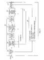
- FIG. 7illustrates another example embodiment process module 701 of the present invention. At least some aspects of the example embodiments of FIG. 7 are similar to the example embodiments illustrated in FIG. 3 with respect to its example processing tools (e.g., implanter tools 1 707 and 2 709 and an annealing tool 711 ) and using a module controller 705 . However, the example embodiments of FIG. 7 includes a post-process metrology tool 715 and additional control mechanisms within its module controller 713 .
- example processing toolse.g., implanter tools 1 707 and 2 709 and an annealing tool 711
- the post process metrology tool 717is configured to receive a wafer that has been processed by, for example, the processing tools 707 , 709 , 711 and to make a Measurement After the Process (MAP), a post process measurement, on the processed wafer.
- MAPis made on, for example, junction depth of a test structure being fabricated on the processed wafer.
- the MAPscan be made on one or more test structures on the processed wafer. In embodiments that the MAP is performed on more than one test structure, the average of the MAPs can be used in a feedback process which is described in detail below.
- FIG. 8illustrates the steps performed by the example embodiments of FIG. 7 of the present invention.
- At least some aspects of the first four stepse.g., the steps of receiving a wafer (step 801 ), measuring a CD (step 803 ), determining parameter values (step 805 ), and performing implant and anneal processes (step 807 )
- the post-processing metrology tool 715makes a MAP (step 809 ).
- the module controller 705may cause one of two different sets of steps be performed after the MAP is made, depending upon: (i) whether the MAP value is within a target range (determined in step 811 ); (ii) whether the MAP is within a correctable range, but it is outside of the target range (determined in step 815 ).
- An example of the target range of, e.g., junction depth,is 300 ⁇ 6 angstroms, and an example of the correctable range is ⁇ 30% of the target range.
- the information relating to the target ranges and correctable rangesis stored in a junction depth calibration database in the module controller 705 . It should be noted that, in at least some embodiments of the present invention, the module controller can decide to instruct the metrology tool 717 not to make the MAP when the wafer is processed properly (e.g., the parameter values stayed within an acceptable range.)
- the processed waferis considered to be correctly processed within an acceptable level of variation.
- the processed waferis then transported to a next process module for subsequence processes, if any (step 813 ).
- settings of the implanter and anneal toolsare checked (step 829 ) by the module/tool monitor 713 .
- the settings of the toolsmay include one or any combination of ion energy, ion dose, ion beam current, anneal temperature and/or anneal ramp up rate.
- An example valuemay be 500 eV for the ion energy setting.
- the module controller 705determines whether or not the settings are correctly set (step 831 ). If not, the module controller 705 either adjusts the settings (step 833 ) or notifies an operator to adjust the settings. After settings have been adjusted or the module controller determines that the settings were set correctly, a new wafer is received and processed (step 835 ).
- steps 829 and 815can be performed in parallel.
- settings of implanting and anneal toolsare checked (step 819 ) by the module/tool monitor 713 .
- the module controller 705determines whether or not the settings are correctly set (step 821 ). If not, the module controller 705 either adjusts the settings (step 823 ) or notifies an operator to adjust the settings. After the settings have been adjusted or the module controller determines that the settings were set correctly, the difference between a target MAP and the measured MAP may be used in determining corrections to the processing conditions for the processed wafer (step 825 ).
- the implant process(es)are performed again on the processed wafer (step 827 ) using the correction parameter values.
- a anneal process(es)can also be re-performed.
- the processed wafer which was incorrectly processedis reprocessed by the process module 601 using the correction parameter values.
- the correction parameter valuescan be determined using a LUT that has been created using similar steps as those used in creating the LUT for parameter values as described above in connection with Table 1.
- the reprocessed wafercan then be transported to a next process module, if any, for further processing.
- the post-process metrology toolcan make another MAP and perform the above-described steps again starting from step 809 .
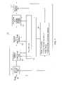
- FIG. 9shows yet another example embodiment process module 901 of the present invention.
- the example embodiment of FIG. 9is, in at least some aspects, similar to the second example embodiment illustrated in FIG. 7 with respect to, e.g., its example processing tools (e.g., the implanter tools 1 907 and 2 911 and the annealing tool 913 ) and creating and using a module controller 905 .
- metrology tools 909 , 913configured to check the dosage of each implementing step are placed between the implanter tool 1 907 and the implanter tool 2 911 and between the implanter tool 2 911 and the annealing tool 915 .
- the metrology tool 909measures the dosage (step 1009 ), if the dosage is within a target range (step 1011 ), then the wafer is sent to the implanter tool 2 911 (step 1015 ). If the measured dosage is not within a target range (e.g., it is under dosed), then the wafer is sent back to the implanter tool 1 907 and reprocessed (step 1013 ).
- An example of an under doseis 70–80% of 1 ⁇ 10 15 Ions/cm 2 .
- a correctable rangecan be defined to determine if the dosage can be corrected. If the measured dosage is within correctable range, then the wafer can be sent back to the implanter tool 1 907 ; however, if the dosage is outside of the correctable range, then the wafer is discarded. Similar processes take place at the metrology tool 913 .
- a dosage checking metrology toolcan be inserted between process tools.
- only one metrology tool to measure the dosagecan be placed between the process tools (e.g., between the implanter tool 2 and the annealing tool).
- FIGS. 10 a–billustrate other steps that can be performed by at least some embodiments of the present invention.
- Each of the steps(steps starting from step 1017 ) is similar to the steps described above in connection with the example embodiment of FIG. 7 of the present invention.
- FIG. 11illustrates an example end result of using the above described steps of measuring the CD, obtaining parameter values from the LUT and using the parameter values to compensate for any undesirable variations.
- the first column of a table 1101lists the parameters relating to gate length affected by variations in a critical dimension.
- the second columnshows percent deviation of values of those parameters when the photoresist is under etched 10 nm.
- Taudeviates 16% and I off deviates 28% and I DSAT deviates 7.45%.
- a parameter of the implante.g., 120% of a baseline SDE dosage is applied.
- the deviation of Tauis reduced to 0.13%.
- I offis increased to 48% and I DSAT is reduced to 5.5% and V T is at 1.92%. This effect can be further improved by applying 120% of SDE dose and additional 10% of halo tilt from their respective baseline conditions.
- the deviation in Tauis reduced to 1.92%, I off is reduced to 9%, I DSAT is reduced to 3.5% and V T is reduced to 1%.
- the parameter and parameter values, results, etc.are all by way of example, and that one, some or all can depend on a variety of factors (e.g., device design and geometry).
- FIG. 12shows the results obtained for deviation in Tau and leakage current when SDE and halo tilt are adjusted to compensate an under etch process (e.g., 10 nm under etch).
- a line with cross-hair marksshows deviation in Tau when no halo tilt is provided and a line with rectangles shows deviation in Tau when 10% halo tilt is provided.
- a line with trianglesshows deviation in leakage current when no halo tilt is provided and a line with circles shows deviation in leakage current when 10% halo tilt is provided.
- Cross points of these lines with 0% deviation linerepresent partially optimal compensations.
- 10% halo tilt and approximately 120% increase in SDE dosagemay yield the lowest deviations in Tau and leakage current.
- the percent deviationis minimal when the SDE dosage is increased by about 120% and the halo tilt was increased by 10%.
- similar compensationscan also be achieved by adjusting other conditions (for example, energy, tilt angle of source drain extension, energy and angle of halo implants, etc.)
- FIG. 13illustrates a block diagram of one example of the internal hardware of (e.g., a module controller 1313 ), which represents any of the above described module controllers 305 , 705 or 905 .
- a bus 1356serves as the main information highway interconnecting various components therein.
- CPU 1358is the central processing unit of the module controller 1313 , performing calculations and logic operations required to execute the control/operation processes of the present invention as well as other programs.
- Read only memory (ROM) 1360 and random access memory (RAM) 1362constitute the main memory of model controller 1313 .
- Disk controller 1364interfaces one or more disk drives to the system bus 1356 . These disk drives are, for example, floppy disk drives 1370 , or CD ROM or DVD (digital video disks) drives 1366 , or internal or external hard drives 1368 . These various disk drives and disk controllers are optional devices.
- a display interface 1372interfaces display 1348 and permits information from the bus 1356 to be displayed on display 1348 .
- Display 1348may be used in displaying various graphs.
- Optical fibers and/or electrical cables and/or conductors and/or optical communication (e.g., infrared, and the like) and/or wireless communication (e.g., radio frequency (RF), and the like)can be used as the transport medium between the external devices and communication port 1374 .
- Peripheral interface 1354interfaces the keyboard 1350 and mouse 1352 , permitting input data to be transmitted to bus 1356 .
- the module controller 1313also optionally includes an infrared transmitter and/or infrared receiver.
- Infrared transmittersare optionally utilized when the computer system is used in conjunction with one or more of the processing components/stations/modules that transmit/receive data via infrared signal transmission.
- the computer systemmay also optionally use a low power radio transmitter 1380 and/or a low power radio receiver 1382 .
- the low power radio transmittertransmits the signal for reception by components of the production process, and receives signals from the components via the low power radio receiver.
- the low power radio transmitter and/or receiverare standard devices in industry.
- the module controller in FIG. 13is illustrated having a single processor, a single hard disk drive and a single local memory
- the analyzeris optionally suitably equipped with any multitude or combination of processors or storage devices.
- the computermay be replaced by, or combined with, any suitable processing system operative in accordance with the principles of embodiments of the present invention, including sophisticated calculators, and hand-held, laptop/notebook, mini, mainframe and super computers, as well as processing system network combinations of the same.
- FIG. 14is an illustration of an example computer readable memory medium 1484 utilizable for storing computer readable code or instructions.
- medium 1484may be used with disk drives illustrated in FIG. 13 .
- memory mediasuch as floppy disks, or a CD ROM, or a digital video disk will contain, for example, a multi-byte locale for a single byte language and the program information for controlling the modeler to enable the computer to perform the functions described herein.
- ROM 1360 and/or RAM 1362 illustrated in FIG. 13can also be used to store the program information that is used to instruct the central processing unit 1358 to perform the operations associated with various automated processes of the present invention.
- suitable computer readable media for storing informationinclude magnetic, electronic, or optical (including holographic) storage, some combination thereof, etc.
Landscapes
- Engineering & Computer Science (AREA)
- Manufacturing & Machinery (AREA)
- Computer Hardware Design (AREA)
- Microelectronics & Electronic Packaging (AREA)
- Power Engineering (AREA)
- Physics & Mathematics (AREA)
- Condensed Matter Physics & Semiconductors (AREA)
- General Physics & Mathematics (AREA)
- Testing Or Measuring Of Semiconductors Or The Like (AREA)
Abstract
Description
The present invention relates to methods, systems and mediums for controlling processes for manufacturing micro-electronic devices based on, in part, one or more measurements made on one or more critical dimensions such as gate lengths of devices. In particular, the measured critical dimensions can be used in determining parameter values in, for example, feed-forward and/or feed-back controlling mechanisms to reduce variations on the critical dimensions.
These undesirable variations are unacceptable due to ever increasing demands on fabricated micro-electronic devices associated with ultra large scale integration that require increased transistor and circuit speed, density and improved reliability. In particular, these demands require formation of device features with high precision and uniformity, which in turn necessitates careful process monitoring and detailed inspection of the devices while they are still being processed in the form of semiconductor wafers. Indeed, theconventional process module 101 is incapable of processing devices with such high precision and uniformity because it cannot reduce the undesirable variations. This results in a device yield rate that is less than optimal.
Embodiments of the present invention advantageously overcome the above described shortcomings of conventional processing modules. In particular, embodiments of the present invention provide systems, methods and mediums for controlling processes for fabricating micro-electronic devices using critical dimension measurements. For instance, at least some embodiments of the present invention include a method of processing a number of wafers for manufacturing semiconductor devices. The method comprises the steps of measuring at least one dimension (e.g., gate length) of at least one of the devices being fabricated on at least one of the wafers and determining control parameter values (also referred to as process conditions) based on the at least one measured dimension. (It should be noted a control parameter value and a parameter value are used interchangeably in describing embodiments of the present invention.) The method may also include the step of controlling at least one semiconductor manufacturing tool to process the at least one of the wafers based on the parameter values (e.g., in a feed-forward/feed-back manner). The at least one processing tool can include at least one implanter tool.
The detailed description of the present application showing various distinctive features may be best understood when the detailed description is read in reference to the appended drawings in which:
To alleviate the shortcomings of the conventional technology, in at least some embodiments of the present invention, the undesirable variations mentioned above can be compensated for by first measuring a critical dimension of a device being processed. A critical dimension (CD) is a dimension of a particular location of a device (e.g., a gate length). Variations in the CD may cause undesirable performance variations on the device. If such variations in a CD are detected, a subsequent processing tool(s) may be adjusted such that the undesirable variation is alleviated. This is done by generating one or more parameter values based upon the amount of the variation. The parameter values are then used by the processing tool(s) to make the appropriate adjustment.
Examples of performance variations are depicted inFIG. 2 , which shows agraph 201 illustrating deviations in device performances caused by variations in CDs of devices. More specifically,FIG. 2 illustrates deviations in a number of parameters that measure performances of produced micro-electronic devices (e.g., microprocessors) having a target for the CD as 130 nm. The parameters include: d Tau, d Ioff, d IDSATand d VT(“d” represents change/deviation). The value of d Tau is deviation in gate delay time, which is defined as C*Vdd/IDSAT(C: capacitance; Vdd: drain voltage; and IDSATsaturation current), the value of d Ioffis deviation in leakage current; the value of d IDSATis deviation in saturation drive current; and the value of d VTis deviation in threshold voltage. As illustrated inFIG. 2 , variations in the CD have a significant impact on device performances. A 10 nm variation (from 130 nm to 140 nm) in the CD is shown as resulting in about a 16% variation in Tau and more than a 30% variation in leakage current (Ioff). Both Tau and Ioffare critical as they affect device speed and battery life, respectively.
As noted above, the conventional processing modules and their process tools are incapable of correcting undesirable variations because, in part, they are not configured to measure CDs and/or use the CD measurements generating/adjusting parameter values.
At least some embodiments of the present invention are shown inFIGS. 3A–B ,7 and9. More specifically, inFIG. 3A–B , anexample module controller 305 that receives CD measurements of one or more devices on a wafer and generates parameter values based thereon is illustrated. InFIG. 7 , anotherexample module controller 705 is illustrated wherein themodule controller 705 receives CD and junction depth measurements and generates parameter values based thereon.FIG. 9 illustrates yet anotherexample module controller 905, wherein themodule controller 905 includes metrology tools for checking dosages. These embodiments are provided only as examples, and various individual components, devices and/or tools of one embodiment can be omitted, added to, and/or combined with other embodiments. Detailed descriptions of these embodiments and other aspects of the present invention are provided below.
Referring toFIG. 3A , this figure illustrates an exampleembodiment process module 301 of the present invention in which critical dimension (CD) measurements are made and the measured CD values are used in controlling one or more processing tools by generating/adjusting parameter values. The example embodiment ofFIG. 3A also includes ametrology tool 303, amodule controller 305, atool monitor 313 and aprocess tool 308.FIG. 3B illustrates a somewhat more specific example embodiment depicting similar concepts. More specifically, the example embodiment depicted inFIG. 3B further includesprocessing tools
Now referring both toFIG. 3A andFIG. 3B , themetrology tool 303 is configured to measure CDs of one or more devices being fabricated on wafers. In at least some embodiments of the present invention, a CD is, for example, gate lengths of devices. In at least some embodiment of the present invention, CDs of devices on all dies of a wafer are measured. The average of the measured CDs is calculated and then communicated to themodule controller 305. In at least some other embodiments, CD measurements are made on a sub-set of dies and their average is calculated and communicated to themodule controller 305. In particular, the sub-set of dies can be a line of dies on a wafer (e.g., a horizontal line, a vertical line or a line of any orientation), a portion of dies on a wafer (e.g., an upper half or an upper left quadrant), any random combination of dies or any one die. Furthermore, it should be understood that gate length is a CD often mentioned herein only by way of example, and that embodiments of the present invention contemplate that a CD can also be any facet or dimension on a device that may cause performance variations in produced devices when it varies from a target by a certain amount.
The set of process tools inFIG. 3B , for example, can include one or any combination of processing tools such as animplanter tool 1307, animplanter tool 2309 and anannealing tool 311. It should also be noted that thetool 308 ofFIG. 3A can be any one of an implanter tool or an annealing tool. In other words, the number of processing tools and their types are not limited to only having, for example, two implanter tools and one annealing tool as shown inFIG. 3B . It should also be noted that the various combinations of implanter and annealing tools do not necessarily represent all the tools that may be required to process a wafer. Other tools that can be included are, for example, photolithography tools, etchers, cleaners, etc. The implanter and annealing tools are illustrated as example tools that can be controlled by themodule controller 305. The process tools, regardless which one of the above-described embodiments is used, are configured to provide various implant process(es), anneal process(es) and/or other process(es) by themodule controller 305 and tool monitor313. In addition, at least some embodiments of the present invention contemplate that the tool monitor313 would be unnecessary, and that, e.g., at least some of the functions provided by the tool monitor313 can be controlled by themodule controller 305 and/or a processing tool, itself.
Embodiments of the present invention can be configured to include any type of implanter tools and annealing tools that can be controlled by using, in part, parameters and specific values thereof. For example, embodiments of the present invention can include any implant and annealing tools such as single wafer and batch tools that include: low energy, high current, medium current, high energy implanters, batch furnace, single RTP annealers, beamline and/or plasma based doping tools.
In the example embodiment shown inFIG. 3B , theimplanter tool 1307 is configured to perform source drain contracts and SDE implants. Theimplanter tool 2309 is configured to perform halo/VT/Well implants. Theimplanter tools annealing tool 311 is Radiance™, manufactured by Applied Materials, Inc. of Santa Clara, Calif. These process tools are provided herein only as examples. Other types of implanter and annealing tools that can thus also be used in embodiments of the present invention. It should be noted that, in addition to themodule controller 305, each processing tool may be coupled to a tool controller502 (shown inFIG. 5 ) configured to control its respective process control and set-up based on information (e.g., process conditions) received from themodule controller 305.
As noted above regardingFIG. 3B , the process tools (e.g., theimplanter tools module controller 305. In this example embodiment, themodule controller 305 is configured to operate/control theimplanter tools annealing tool 311 using parameter values. In particular, based on CD measurements, themodule controller 305 determines appropriate values for parameter values. Examples of parameters (for which values can be obtained) include a halo angle, a dose and energy level, a Source-Drain-Extension (SDE) dose level, an energy and tilt level, a pocket implant dose level, a channel and channel VTadjust implant dose level, an energy and tilt level, a Rapid Thermal Processing (RTP) peak temperature level, and/or anneal time length.
In order to provide the context in which the parameter values may be determined, an example of CD measurements is illustrated. In this example, the critical dimension is measured by themetrology tool 303. The measured CD can be different from a target CD (thus, possibly indicating the existence of an undesirable variation). For instance, as graphically shown inFIG. 4 , a device may have been erroneously processed such that a measured CD (in this example, gate length)403 is wider than atarget 401, which may have been caused by aphotoresist layer 405 that has been underetched in a previous processing step. Thewider gate length 403 in turn can introduce undesirable variation into other aspects of devices such as effective channel length (e.g., it may cause a wider effective channel length412). For example, had the gate length met thetarget gate length 401, the effective channel length would have met a targeteffective channel length 411. However, due to thewider gate length 403, the measured effective channel length is wider than the target effective channel length. When only baseline parameter values are used as in the conventional process module inFIG. 1 , this undesirable variation cannot be compensated for. However, embodiments of the present invention can compensate for this undesirable variation by determining parameter values (based on the gate length) and using them to modify the operation of one or more processing tools to form final effective channel length to be substantially identical/similar to the target effective channel length.
Before explaining how the parameter values are obtained and used, the step of creating parameter values as contemplated by at least some embodiments of the present invention is first described. In at least one example embodiment, themodule controller 305 includes a technique for determining parameter values based on measured CD values. The parameter values can then be stored in an active channel control lookup table (LUT). The parameter values for the LUT are created, for example, by using a computer implemented simulation package (e.g., T CAD, manufactured by Integrated System Engineering, ISE, of Switzerland). In particular, the simulation package can be configured to generate (e.g., calculate) values of parameters for a particular CD measurement. In other words, in this example embodiment, the simulation package is configured to generate values of parameters (e.g., SDE, halo and RTP process conditions) for a particular gate length measurement in order to compensate for any CD variations (e.g., an over or under etching). In this way, an array of values of SDE, halo and RTP conditions are created for a series of gate lengths at a predetermined interval (e.g., every 0.1 nm, 1 nm or multiple nms of gate lengths). The array of parameter values along with their corresponding measured CD values is then collected into the LUT, which is then used to lookup a corresponding set of parameter values for any measured gate length. An example of the LUT is shown below in Table 1.
| TABLE 1 | |||
| Measured | SDE Implant | Halo Implant | Anneal (RTP) |
| Gate | Specie | Specie | Peak | Ramp | |||||||
| length CD | type | E | Dose | tilt/ | type | E | Dose | tilt | twist | Temp | up/cooldown |
| (nm) | (Boron) | (keV) | (ion/cm{circumflex over ( )}2) | twist | (Arsenic) | (keV) | (ion/cm{circumflex over ( )}2) | (degree) | (degree) | (C.) | rate (C/sec) |
| 70 | B | 0.4 | 1.00E+15 | 0, 0 | As | 30 | 5.00E+13 | 22 | 0 | 1050 | 250/90 |
| 75 | B | 0.45 | 7.50E+14 | 0, 0 | As | 30 | 5.00E+13 | 24 | 0 | 1050 | 250/90 |
| 80 | B | 0.45 | 1.00E+15 | 0, 0 | As | 30 | 5.00E+13 | 26 | 0 | 1050 | 250/90 |
| 85 | B | 0.5 | 7.50E+14 | 0, 0 | As | 30 | 5.00E+13 | 28 | 0 | 1050 | 250/90 |
| 90 | B | 0.5 | 1.00E+15 | 0, 0 | As | 30 | 5.00E+13 | 30 | 0 | 1050 | 250/90 |
| 95 | B | 0.5 | 1.25E+15 | 0, 0 | As | 30 | 5.00E+13 | 32 | 0 | 1050 | 250/90 |
| 100 | B | 0.55 | 1.00E+15 | 0, 0 | As | 30 | 5.00E+13 | 34 | 0 | 1050 | 250/90 |
| 105 | B | 0.55 | 1.25E+15 | 0, 0 | As | 30 | 5.00E+13 | 36 | 0 | 1050 | 250/90 |
| 110 | B | 0.6 | 1.00E+15 | 0, 0 | As | 30 | 5.00E+13 | 38 | 0 | 1050 | 250/90 |
In the above table, “E (keV),” “Dose,” “tilt/twist,” “peak temperature” and “up/cooldown rate” are example parameters and the entries of the table are example parameter values.
In at least some embodiments of the present invention, the LUT created using the simulation package is refined based on empirical data collected by performing experiments. In such an example embodiment, a set of test wafers is fabricated to form devices having different average gate lengths. The test wafers are then put through the processes by theimplanter tools FIG. 3B ) using the parameter values of the LUT by the module controller for that particular measured CD. When the test wafers are processed, the results are collected and compared against predicted results by the simulation package. If the test wafers are processed to produce devices with the predicted results, then no adjustment on the parameter values is made to the LUT. If not, then the LUT entry is replaced or adjusted in accordance with the data collected during the experiments. These steps of comprising/replacing the entries of the LUT can be repeated until all the entries of the LUT are checked/adjusted.
In at least some embodiments of the present invention, a number of LUTs can be created, each of which may relate to device types and/or technology nodes. Device types can be microprocessors, memory chips, programmable ROMs, etc. A technology node can be a 100 nm node, a 130 nm node, a 180 nm node, etc. In at least some embodiments of the present invention, a LUT can also be created using only experimental data without using a computer simulation package.
In at least some embodiments of the present invention, instead of a LUT, one or more equations are derived to determine the parameter values for measured CDs. In yet other embodiments of the present invention, a graphical representation may be used in determining the parameter values for measured CDs. It should be noted that the present invention can use a LUT, one or more equations, one or more graphical representations, or other mechanisms for determining parameter values.
Now turning to describe themodule controller 305 and tool monitor313 in more detail,FIG. 5 is a block diagram illustrating some example operations of themodule controller 305 and tool monitor313. More specifically, themodule controller 305 can be configured to include an active channel control LUT. Embodiments of the present invention contemplate that themodule controller 305 can also (or alternatively) use an external LUT to receive or determine parameter values (step501). In any of these example embodiments, and in accordance with the example of Table 1 (for purposes of discussion), themodule controller 305 then uses the parameter values of “SDE implant” from the LUT to control the implanter tool1 (step503) and uses the parameter values of “halo implant” from the LUT to control the implanter tool2 (step505). Themodule controller 305 uses the parameter values of RTP from the LUT to control the annealing tool (step507). As indicated previously, steps such as those can be used to compensate an undesirable variance within devices on a wafer caused by some previous process step (e.g., lithography, photoresist and/or etching process steps) performed by a previous manufacturing tool. Consequently, these mechanisms of controlling the process tools based on parameter values from the LUT are referred to as feed-forward control mechanisms.
While the process tools are being operated and/or controlled by themodule controller 305, at least some embodiments of the present invention contemplate that thetool monitor 313 is configured to monitor activities of each process tool (step509). Themodule controller 305 can also be configured to adjust parameter values and setups of the process tools based on the results of themonitoring step 509 by the tool monitor (step511). Examples of setups of the process tools can be one or any combination of a beam-current, a vacuum pressure, tool pressure, tool temperature, etc.
In the above-described example embodiments, the feed-forward control mechanism of themodule controller 305 uses three parameter values (i.e., SDE, halo and RTP conditions) to operate/control three process tools. As noted above, the SDE parameter is used to control theimplanter tool 1, the halo parameter is used to controlimplanter 2, and the RTP parameter is used in controlling the annealing tool. In at least some embodiments of the present invention, not all parameter values may be required. In particular, In at least one example embodiment, only the SDE parameter may be determined by using the LUT andonly implanter tool 1 is controlled by the feed-forward control mechanism. In such an embodiment, other tools (i.e., theimplanter tool 2 and the annealing tool), if they are present at all, would not be controlled using feed-forward parameter values, but would be controlled by, for example, the conventional control mechanism as described above in connection withFIG. 1 (i.e., using only baseline parameter values). In another example embodiment, only the halo parameter may be determined for theimplanter 2, or only the RTP parameter may be determined for the annealing tool. In addition, embodiments of the present invention contemplate that any combination of two process tools can also be controlled by their respective parameter values. Accordingly, the present invention is not limited by having to use any specific number of parameter values. InFIG. 3B ,lines 312 from themodule controller 305 to the process tools are dotted rather than solid in order to represent that one, two or three of the process tools can be controlled by the feed-forward control mechanism. This dotted-line representation is also applicable to subsequent example embodiments depicted inFIGS. 7 and 9 . It should also be understood that the specific parameters and associated values corresponding to the particular types of tools mentioned (i.e., implanter tools and annealing tools) are also by way of example, and that any number of other types of appropriate parameters and corresponding values are also contemplated by at least some embodiments of the present invention.
Referring to the above-described example embodiments ofFIG. 3B , using Table 1 to control each of the 3 tools mentioned therein, themodule controller 305 of these embodiments are configured (in at least some embodiments of the present invention) to conduct steps shown inFIG. 6 . The steps include receiving a wafer (step601), measuring a critical dimension of one or more devices as described above (step603), determining parameter values (step605), and performing implant and anneal processes based on the results obtained by conducting the step of determining parameter values (step607).
In the step of receiving a wafer (step601), the wafer may be received from a batch of wafers, which are being fabricated to form a number of micro-electronic devices thereon.
In the step of measuring a critical dimension (CD) (step603), a CD of a device, which can relate to a part of one or more micro-electronic devices, is measured. In at least some embodiments of the present invention, the CD can be the gate length of a selected device. In at least some other embodiments of the present invention, the CD can be an average of the gate lengths measured from many devices or test structures on the received wafer. The test structure can be a number of polysilicon lines fabricated on the wafers. The dimension of the test structure may be similar to those of devices fabricated on the wafers.
The measured CD is then received by themodule controller 305, which performs the step of determining appropriate parameter values (step605). As noted above in connection withFIG. 3 , this step can be performed using a LUT, one or more equations, and/or graphical representations.
Themodule controller 305 then performs the step of operating/controlling the process tools (e.g., implantedtools
The results of such processing are graphically illustrated inFIG. 4 . After processing by the process tools using the parameter (e.g., increased halo tilt409), what might have been a wideeffective channel length 412 is compensated to be closer to the targeteffective channel length 411.
The postprocess metrology tool 717 is configured to receive a wafer that has been processed by, for example, theprocessing tools
When the MAP is within the target range, the processed wafer is considered to be correctly processed within an acceptable level of variation. The processed wafer is then transported to a next process module for subsequence processes, if any (step813).
When the MAP is outside of the target range, for processing subsequent wafers, settings of the implanter and anneal tools are checked (step829) by the module/tool monitor 713. Examples of the settings of the tools may include one or any combination of ion energy, ion dose, ion beam current, anneal temperature and/or anneal ramp up rate. An example value may be 500 eV for the ion energy setting. Themodule controller 705 determines whether or not the settings are correctly set (step831). If not, themodule controller 705 either adjusts the settings (step833) or notifies an operator to adjust the settings. After settings have been adjusted or the module controller determines that the settings were set correctly, a new wafer is received and processed (step835).
With respect to the wafer that has been processed and its MAP has been determined as outside of the target range and outside of the correctable range, the processed wafer is considered as not usable and discarded (step817). It should be noted thatsteps
When the wafer that has been processed and its MAP has been determined as outside of the target range but within the correctable range, settings of implanting and anneal tools are checked (step819) by the module/tool monitor 713. Themodule controller 705 determines whether or not the settings are correctly set (step821). If not, themodule controller 705 either adjusts the settings (step823) or notifies an operator to adjust the settings. After the settings have been adjusted or the module controller determines that the settings were set correctly, the difference between a target MAP and the measured MAP may be used in determining corrections to the processing conditions for the processed wafer (step825). Subsequently, the implant process(es) are performed again on the processed wafer (step827) using the correction parameter values. (For example, a anneal process(es) can also be re-performed.) In other words, the processed wafer which was incorrectly processed is reprocessed by theprocess module 601 using the correction parameter values. The correction parameter values can be determined using a LUT that has been created using similar steps as those used in creating the LUT for parameter values as described above in connection with Table 1.
The reprocessed wafer can then be transported to a next process module, if any, for further processing. Alternatively, the post-process metrology tool can make another MAP and perform the above-described steps again starting fromstep 809.
In operation (and referring also toFIG. 10 a), after a doping step by theimplanter tool 1907, themetrology tool 909 measures the dosage (step1009), if the dosage is within a target range (step1011), then the wafer is sent to theimplanter tool 2911 (step1015). If the measured dosage is not within a target range (e.g., it is under dosed), then the wafer is sent back to theimplanter tool 1907 and reprocessed (step1013). An example of an under dose is 70–80% of 1×10¹⁵Ions/cm2.
In an alternative embodiment, a correctable range can be defined to determine if the dosage can be corrected. If the measured dosage is within correctable range, then the wafer can be sent back to theimplanter tool 1907; however, if the dosage is outside of the correctable range, then the wafer is discarded. Similar processes take place at themetrology tool 913.
It should be noted that similar modifications can be made to the example embodiment ofFIGS. 3A ,3B and7. For example, in a modified embodiment ofFIG. 3B , a dosage checking metrology tool can be inserted between process tools. In at least some other embodiments of the present invention, only one metrology tool to measure the dosage can be placed between the process tools (e.g., between theimplanter tool 2 and the annealing tool).
In the above-described example embodiments, various components and steps have been illustrated and described. Relating to those example embodiments,FIG. 11 illustrates an example end result of using the above described steps of measuring the CD, obtaining parameter values from the LUT and using the parameter values to compensate for any undesirable variations.
The first column of a table1101 lists the parameters relating to gate length affected by variations in a critical dimension. The second column shows percent deviation of values of those parameters when the photoresist is under etched 10 nm. When uncompensated parameter values are used, Tau deviates 16% and Ioffdeviates 28% and IDSATdeviates 7.45%. When a parameter of the implant is compensated, e.g., 120% of a baseline SDE dosage is applied. The deviation of Tau is reduced to 0.13%. However, Ioffis increased to 48% and IDSATis reduced to 5.5% and VTis at 1.92%. This effect can be further improved by applying 120% of SDE dose and additional 10% of halo tilt from their respective baseline conditions. When the compensated parameter values are used, the deviation in Tau is reduced to 1.92%, Ioffis reduced to 9%, IDSATis reduced to 3.5% and VTis reduced to 1%. It should be understood that the parameter and parameter values, results, etc. are all by way of example, and that one, some or all can depend on a variety of factors (e.g., device design and geometry).
Graphical illustrations of improvements in at least some embodiments of the present invention are provided inFIG. 12 , which shows the results obtained for deviation in Tau and leakage current when SDE and halo tilt are adjusted to compensate an under etch process (e.g., 10 nm under etch). In particular, a line with cross-hair marks shows deviation in Tau when no halo tilt is provided and a line with rectangles shows deviation in Tau when 10% halo tilt is provided. Also, a line with triangles shows deviation in leakage current when no halo tilt is provided and a line with circles shows deviation in leakage current when 10% halo tilt is provided. Cross points of these lines with 0% deviation line represent partially optimal compensations.
In at least some embodiments of the present invention, for the lowest deviation in leakage current: 1) no halo tilt and approximately 60% increase in SDE dosage (point1203); and 2) 10% halo tilt and approximately 110% increase in SDE dosage (point1205).
For the lowest deviation in Tau: 1) no halo tilt and approximately 120% increase in SDE dosage (point1205); and 2) 10% halo tilt and approximately 140% increase in SDE dosage (point1207).
Based on the above observations, 10% halo tilt and approximately 120% increase in SDE dosage may yield the lowest deviations in Tau and leakage current. For example, the percent deviation is minimal when the SDE dosage is increased by about 120% and the halo tilt was increased by 10%. It should be noted that similar compensations can also be achieved by adjusting other conditions (for example, energy, tilt angle of source drain extension, energy and angle of halo implants, etc.)
An example embodiment of the computer on which any of the module controller embodiments of various other aspects of the present invention may operate is described below in connection withFIGS. 13–14 .
Adisplay interface 1372 interfaces display1348 and permits information from thebus 1356 to be displayed ondisplay 1348.Display 1348 may be used in displaying various graphs. Communications with external devices, such as the other components of the system described above, occur utilizing, for example,communication port 1374. Optical fibers and/or electrical cables and/or conductors and/or optical communication (e.g., infrared, and the like) and/or wireless communication (e.g., radio frequency (RF), and the like) can be used as the transport medium between the external devices andcommunication port 1374.Peripheral interface 1354 interfaces thekeyboard 1350 andmouse 1352, permitting input data to be transmitted tobus 1356. In addition to these components, themodule controller 1313 also optionally includes an infrared transmitter and/or infrared receiver. Infrared transmitters are optionally utilized when the computer system is used in conjunction with one or more of the processing components/stations/modules that transmit/receive data via infrared signal transmission. Instead of utilizing an infrared transmitter or infrared receiver, the computer system may also optionally use a lowpower radio transmitter 1380 and/or a lowpower radio receiver 1382. The low power radio transmitter transmits the signal for reception by components of the production process, and receives signals from the components via the low power radio receiver. The low power radio transmitter and/or receiver are standard devices in industry.
Although the module controller inFIG. 13 is illustrated having a single processor, a single hard disk drive and a single local memory, the analyzer is optionally suitably equipped with any multitude or combination of processors or storage devices. For example, the computer may be replaced by, or combined with, any suitable processing system operative in accordance with the principles of embodiments of the present invention, including sophisticated calculators, and hand-held, laptop/notebook, mini, mainframe and super computers, as well as processing system network combinations of the same.
In general, it should be emphasized that the various components of embodiments of the present invention can be implemented in hardware, software or a combination thereof. In such embodiments, the various components and steps would be implemented in hardware and/or software to perform the functions of embodiments of the present invention. Any presently available or future developed computer software language and/or hardware components can be employed in such embodiments of the present invention. For example, at least some of the functionality mentioned above could be implemented using Visual Basic, C, C++, or any assembly language appropriate in view of the processor(s) being used. It could also be written in an interpretive environment such as Java and transported to multiple destinations to various users.
The many features and advantages of embodiments of the present invention are apparent from the detailed specification, and thus, it is intended by the appended claims to cover all such features and advantages of the invention which fall within the true spirit and scope of the invention. In addition, it should be understood that aspects of the various embodiments and alternative embodiments mentioned therein can overlap and be combined, forming additional embodiments that are also contemplated herein. Further, since numerous modifications and variations will readily occur to those skilled in the art, it is not desired to limit the invention to the exact construction and operation illustrated and described, and accordingly, all suitable modifications and equivalents may be resorted to, falling within the scope of the invention.
Claims (44)
1. A method of processing a plurality of wafers for manufacturing semiconductor devices, the method sequentially comprising:
(a) measuring at least one critical dimension of at least one device fabricated on at least one of the plurality of wafers by a metrology tool of an implant-annealing process module before the at least one of the plurality of wafers has been processed in at least one implant or annealing processing tool of the implant-annealing process module, wherein a variation in the at least one critical dimension causes a variation in performance of the at least one device;
(b) determining at least one control parameter value of the at least one implant or annealing processing tool based on the measured at least one critical dimension, wherein the at least one control parameter value is selected from the group that consists of a halo angle, a Source Drain-Extension (SDE) dose level, an energy and tilt level, a pocket implant dose level, and a channel and channel VTadjust implant dose level;
(c) controlling the at least one implant or annealing processing tool of the implant-annealing process module to process the at least one of the plurality of wafers based on the at least one control parameter value;
(d) measuring at least one post process dimension of the at least one of the plurality of wafers after step (c), wherein the measured at least one post process dimension is different than the measured at least one critical dimension;
(e) determining whether the measured at least one post process dimension is within a first predetermined range; and
(f) adjusting the at least one implant or annealing processing tool of the implant-annealing process module upon determining that the measured at least one post process dimension is not within the first predetermined range.
2. The method ofclaim 1 , wherein the at least one post process dimension is a junction depth and the method further comprises:
(g) sending the at least one of the plurality of wafers to a next processing tool upon determining that the at least one post process dimension is within the first predetermined range.
3. The method ofclaim 1 wherein the at least one critical dimension is a gate length.
4. The method ofclaim 1 , wherein the at least one implant or annealing processing tool includes at least one implanter tool for implanting ions into a junction of said at least one device for at least reducing deviation in gate delay.
5. The method ofclaim 4 , wherein the at least one implanter tool is a beamline type implanting tool.
6. The method ofclaim 1 , wherein the first predetermined range is plus or minus 10 percent from a respective target value.
7. The method ofclaim 1 , further comprising:
forming the at least one critical dimension prior to measuring at least one critical dimension.
8. The method ofclaim 4 , wherein the at least one implanter tool processes one wafer at a time.
9. The method ofclaim 1 , wherein the at least one implant or annealing processing tool includes at least one annealing tool for at least reducing deviation in gate delay.
10. The method ofclaim 9 , wherein the annealing tool is controlled by parameters that include at least one of a Rapid Thermal Processing (RTP) peak temperature level and anneal time length.
11. An implant-annealing process module comprising:
a first metrology tool configured to measure at least one critical dimension of at least one device fabricated on at least one of a plurality of wafers before the at least one of the plurality of wafers is processed by at least one implant or annealing processing tool of the implant-annealing process module, wherein a variation in the at least one critical dimension causes a variation in performance of the at least one device;
a module controller configured to determine at least one control parameter value of the implant or annealing processing tool based on the measured at least one critical dimension, wherein the at least one implant or annealing processing tool of the implant-annealing process module is configured to be controlled by the module controller in processing the at least one of the plurality of wafers based on the at least one control parameter value and wherein the at least one control parameter value determined by the module controller is selected from the group that consists of a halo angle, a Source Drain-Extension (SDE) dose level, an enemy and tilt level, a pocket implant dose level, and a channel and channel VTadjust implant dose level; and
a second metrology tool configured to measure at least one post process dimension of the at least one of the plurality of wafers, wherein the at least one post process dimension is different from the at least one critical dimension and wherein the module controller is further configured to determine whether the measured at least one post process dimension is within a first predetermined range and the module controller is further configured to adjust the at least one implant or annealing processing tool of the implant-annealing process module upon determining that the measured at least one post process dimension is not within the first predetermined range.
12. The implant-anneallng process module ofclaim 11 wherein the at least one post process dimension is junction depth.
13. The implant-annealing process module ofclaim 11 wherein the module controller is further configured to adjust at least one parameter value to re-process the at least one of the plurality of wafers when the measured at least one post process dimension is not within the first predetermined range and configured to cause the at least one of the plurality of wafers to be sent to a next processing tool upon determining that the measured at least one post process dimension is within the first predetermined range.
14. The implant-annealing process module ofclaim 11 wherein the first metrology tool is further configured to measure a length of a gate of at least one device fabricated on the at least one of the plurality of wafers.
15. The implant-annealing process module ofclaim 11 , wherein the at least one implant or annealing processing tool includes at least one implanter tool for implanting ions into a junction of said at least one device for at least reducing deviation in gate delay.
16. The implant-annealing process module ofclaim 15 , wherein the at least one Implanting tool is a beamline type implanting tool.
17. The implant-annealing process module ofclaim 12 , wherein the first predetermined range is plus or minus 10 percent from a respective target value.
18. The system ofclaim 15 , wherein the at least one implanter tool processes one wafer at a time.
19. The system ofclaim 11 , wherein the at least one implant or annealing processing tool includes at least one annealing tool for at least reducing deviation in gate delay.
20. The system ofclaim 19 , wherein the annealing tool is controlled by parameters that include at least one of a Rapid Thermal Processing (RTP) peak temperature level and anneal time length.
21. A system of processing a plurality of wafers for manufacturing semiconductor devices, comprising:
means for forming at least one critical dimension on at least one device being fabricated on at least one of the plurality of wafers;
means for measuring the at least one critical dimension of the at least one device being fabricated on the at least one of the plurality of wafers after the at least one critical dimension has been formed, wherein the means for measuring the at least one critical dimension is in an implant-annealing process module and before the at least one of the plurality of wafers is processed by at least one implant or annealing processing tool of the implant-annealing process module, wherein a variation in the at least one critical dimension causes a variation in performance of the at least one device;
means for determining at least one control parameter value of the at least one implant or annealing processing tool based on the measured at least one critical dimension, wherein the at least one control parameter value is selected from the group that consists of a halo angle, a Source Drain-Extension (SDE) dose level, an energy and tilt level, a pocket implant dose level, and a channel and channel VTadjust implant dose level;
means for controlling the at least one implant or annealing processing tool of the implant-annealing process module to process the at least one of the plurality of wafers based on the at least one control parameter value;
means for measuring at least one post process dimension of the at least one of the plurality of wafers, wherein the at least one post process dimension is junction depth and is different from the at least one critical dimension;
means for determining whether the measured at least one post process dimension is within a first predetermined range; and
means for sending the at least one of the plurality of wafers to a next processing tool upon determining that the measured at least one post process dimension is within the first predetermined range.
22. The system ofclaim 21 further comprising:
means for adjusting the at least one implant or annealing processing tool of the implant-annealing process module upon determining that the measured at least one post process dimension is not within the first predetermined range.
23. The system ofclaim 21 further comprising:
means for adjusting at least one parameter value to re-process the at least one of the plurality of wafers when the measured at least one post process dimension is not within the first predetermined range.
24. The system ofclaim 21 wherein the means for measuring at least one critical dimension comprises:
means for measuring a length of a gate on the one of the plurality of wafers.
25. The system ofclaim 21 , wherein the at least one implant or annealing processing tool includes at least one implanter tool for implanting ions into a junction of said at least one device for at least reducing deviation in gate delay.
26. The system ofclaim 25 , wherein the at least one implanting tool is a beamline type implanting tool.
27. The system ofclaim 22 , wherein the first predetermined range is plus or minus 10 percent from a respective target value.
28. The system ofclaim 25 , wherein the at least one implanter tool processes one wafer at a time.
29. The system ofclaim 21 , wherein the at least one implant or annealing processing tool includes at least one annealing tool for at least reducing deviation in gate delay.
30. The system ofclaim 29 , wherein the annealing tool is controlled by parameters that include at least one of a Rapid Thermal Processing (RTP) peak temperature level and anneal time length.
31. A computer-readable medium including instructions being executed by one or more computers, the instructions instructing the one or more computers and at least one metrology tool of an implant-annealing process module and at least one implant or annealing processing tool of the implant-annealing process module for processing a plurality of wafers for manufacturing semiconductor devices, the instructions comprising implementation of the sequential steps of:
(a) measuring at least one critical dimension of at least one device fabricated on at least one of the plurality of wafers by one of the at least one metrology tool of the implant-annealing process module, wherein a variation in the at least one critical dimension causes a variation in performance of the at least one device;
(b) determining at least one control parameter value of the at least one implant or annealing processing tool based on the measured at least one critical dimensions wherein the at least one control parameter value is selected from the group that consists of a halo angle, a Source Drain-Extension (SDE) dose level, an enemy and tilt level, a pocket implant dose level, and a channel and channel VT adjust implant dose level;
(c) controlling the at least one implant or annealing processing tool of the implant-annealing process module to process the at least one of the plurality of wafers based on the at least one control parameter value;
(d) measuring at least one post process dimensions of the at least one of the plurality of wafers by one of the at least one metrology tool of the implant-annealing process module, wherein the at least one post process dimension is junction depth and is different from the at least one critical dimension; and
(e) determining whether the measured at least one post process dimension is within a first predetermined range.
32. The medium ofclaim 31 further comprising instructions to implement the step of:
(f) adjusting the at least one implant or annealing processing tool of the step (c) upon determining that the measured at least one post process dimension is not within the first predetermined range.
33. The medium ofclaim 31 further comprising instructions to implement the steps of:
(f) sending the at least one of the plurality of wafers to a next processing tool upon determining that the measured at least one past process dimension is within the first predetermined range; and
(g) adjusting the step (c) to re-process the at least one of the plurality of wafers when the measured at least one post process dimension is not within the first predetermined range.
34. The medium ofclaim 31 wherein step (a) comprises the step of:
measuring a length of a gate on the one of the plurality of wafers.
35. The medium ofclaim 31 , wherein the at least one implant or annealing processing tool includes at least one implanter tool for implanting ions into a junction of said at least one device for at least reducing deviation in gate delay.
36. The medium ofclaim 35 , wherein the at least one implanting tool is a beamline type implanting tool.
37. The medium ofclaim 31 , wherein, in step (e), the first predetermined range is plus or minus 10 percent from a respective target value.
38. The medium ofclaim 35 , wherein the at least one implanter tool processes one wafer at a time.
39. The medium ofclaim 31 , wherein the at least one implant or annealing processing tool includes at least one annealing tool for at least reducing deviation in gate delay.
40. The medium ofclaim 39 , wherein the annealing tool is controlled by parameters that include at least one of a Rapid Thermal Processing (RTP) peak temperature level and anneal time length.
41. A method of processing a plurality of wafers for manufacturing semiconductor devices, sequentially comprising:
(a) measuring at least one critical dimension of at least one device fabricated on at least one of the plurality of wafers by one of the at least one metrology tool of an implant-annealing process module, wherein a variation in the at least one critical dimension causes a variation in performance of the at least one device;
(b) determining at least one control parameter value of at least one implant or annealing processing tool of the implant-annealing process module based on the measured at least one critical dimension, wherein the at least one control parameter value is selected from the group that consists of a halo angle, a Source Drain-Extension (SDE) dose level, an enemy and tilt level, a pocket implant dose level, and a channel and channel VTadjust implant dose level;
(c) controlling the at least one implant or annealing processing tool of the implant-annealing process module to process the at least one of the plurality of wafers based on the at least one control parameter value;
(d) measuring at least one post process dimension of the at least one of the plurality of wafers by one of the at least one metrology tool of the implant-annealing process module, wherein the at least one post process dimension is junction depth and is different from the at least one critical dimension;
(e) determining whether the measured at least one post process dimension is within a first predetermined range;
(f) sending the at least one of the plurality of wafers to a next processing tool upon determining that the measured at least one post process dimension is within the first predetermined range; and
(g) adjusting the at least one implant or annealing processing tool upon determining that the measured at least one post process dimension is not within the first predetermined range, to thereby reduce deviation in gate delay.
42. A method of processing a plurality of wafers for manufacturing semiconductor devices, sequentially comprising:
(a) measuring at least one critical dimension of at least one device fabricated on at least one of the plurality of wafers by one of the at least one metrology tool of an implant-annealing process module, wherein a variation in the at least one critical dimension causes a variation in performance of the at least one device;
(b) determining at least one control parameter value of at least one implant or annealing processing tool of the implant-annealing process module based on the measured at least one critical dimension, wherein the at least one control parameter value is selected from the group that consists of a halo angle, a Source Drain-Extension (SDE) dose level, an enemy and tilt level, a pocket implant dose level, and a channel and channel VTadjust implant dose level;
(c) controlling the at least one implant or annealing processing tool of the implant-annealing process module to process the at least one of the plurality of wafers based on the at least one control parameter value;
(d) measuring at least one post process dimension of the at least one of the plurality of wafers by one of the at least one metrology tool of the implant-annealing process module, wherein the at least one post process dimension is junction depth and is different from the at least one critical dimension;
(e) determining whether the measured at least one post process dimension is within a first predetermined range; and
(f) re-processing the at least one of the plurality of wafers when the measured at least one post process dimension is not within the first predetermined range, to thereby reduce deviation in gate delay.
43. A semiconductor wafer processing system comprising:
a first metrology tool, of an implant-annealing process module, configured to measure at least one critical dimension of at least one device fabricated on at least one of a plurality of wafers, wherein a variation in the at least one critical dimension causes a variation in performance of the at least one device;
a module controller configured to determine at least one control parameter value based on the measured at least one critical dimension, wherein the at least one control parameter value is selected from the group that consists of a halo angle, a Source Drain-Extension (SDE) dose level, an energy and tilt level, a pocket implant dose level, and a channel and channel VTadjust implant dose level;
at least one implant or annealing processing tool, of the implant-annealing process module, configured to be controlled by the module controller in processing the at least one of the plurality of wafers based on the at least one control parameter value; and
a second metrology tool, of the implant-annealing process module, configured to measure at least one post process dimension of the at least one of the plurality of wafers, wherein the at least one post process dimension is junction depth and is different from the at least one critical dimension;
wherein the module controller is further configured to determine whether the measured at least one post process dimension is within a first predetermined range, configured to cause the at least one of the plurality of wafers to be sent to a next processing tool upon determining that the measured at least one post process dimension is within the first predetermined range, and configured to adjust the at least one implant or annealing processing tool, of the implant-annealing process module, upon determining that the measured at least one post process dimension is not within the first predetermined range, to thereby reduce deviation in gate delay.
44. A semiconductor wafer processing system comprising:
a first metrology tool, of an implant-annealing process module, configured to measure at least one critical dimension of at least one device fabricated on at least one of a plurality of wafers, wherein a variation in the at least one critical dimension causes a variation in performance of the at least one device;
a module controller configured to determine at least one control parameter value based on the measured at least one critical dimension wherein the at least one control parameter value is selected from the group that consists of a halo angle, a Source Drain-Extension (SDE) dose level, an energy and tilt level, a pocket implant dose level, and a channel and channel VTadjust implant dose level; and
a first implant or annealing processing tool, of an implant-annealing process module, configured to be controlled by the module controller in processing the at least one of the plurality of wafers based on the at least one control parameter value, wherein the module controller is further configured to collect measurement of at least one post process dimension of the at least one of a plurality of wafers, wherein the at least one post process dimension is junction depth and is different from the at least one critical dimension, configured to determine whether or not the measured at least one post process dimension is within a first predetermined range, and configured to adjust the at least one parameter value to re-process the one of at least one of the plurality of wafers when the measured at least one post process dimension is not within the first predetermined range to thereby reduce deviation in gate delay.
Priority Applications (5)
| Application Number | Priority Date | Filing Date | Title |
|---|---|---|---|
| US10/100,184US7225047B2 (en) | 2002-03-19 | 2002-03-19 | Method, system and medium for controlling semiconductor wafer processes using critical dimension measurements |
| KR1020047014750AKR101018618B1 (en) | 2002-03-19 | 2003-03-19 | Method, system and medium for controlling semiconductor wafer processes using critical dimension measurements |
| AU2003218285AAU2003218285A1 (en) | 2002-03-19 | 2003-03-19 | Method, system and medium for controlling semiconductor wafer processes using critical dimension measurements |
| PCT/US2003/008513WO2003081513A1 (en) | 2002-03-19 | 2003-03-19 | Method, system and medium for controlling semiconductor wafer processes using critical dimension measurements |
| US11/736,350US20070288116A1 (en) | 2002-03-19 | 2007-04-17 | Method, system and medium for controlling semiconductor wafer processes using critical dimension measurements |
Applications Claiming Priority (1)
| Application Number | Priority Date | Filing Date | Title |
|---|---|---|---|
| US10/100,184US7225047B2 (en) | 2002-03-19 | 2002-03-19 | Method, system and medium for controlling semiconductor wafer processes using critical dimension measurements |
Related Child Applications (1)
| Application Number | Title | Priority Date | Filing Date |
|---|---|---|---|
| US11/736,350DivisionUS20070288116A1 (en) | 2002-03-19 | 2007-04-17 | Method, system and medium for controlling semiconductor wafer processes using critical dimension measurements |
Publications (2)
| Publication Number | Publication Date |
|---|---|
| US20030180972A1 US20030180972A1 (en) | 2003-09-25 |
| US7225047B2true US7225047B2 (en) | 2007-05-29 |
Family
ID=28039750
Family Applications (2)
| Application Number | Title | Priority Date | Filing Date |
|---|---|---|---|
| US10/100,184Expired - LifetimeUS7225047B2 (en) | 2002-03-19 | 2002-03-19 | Method, system and medium for controlling semiconductor wafer processes using critical dimension measurements |
| US11/736,350AbandonedUS20070288116A1 (en) | 2002-03-19 | 2007-04-17 | Method, system and medium for controlling semiconductor wafer processes using critical dimension measurements |
Family Applications After (1)
| Application Number | Title | Priority Date | Filing Date |
|---|---|---|---|
| US11/736,350AbandonedUS20070288116A1 (en) | 2002-03-19 | 2007-04-17 | Method, system and medium for controlling semiconductor wafer processes using critical dimension measurements |
Country Status (4)
| Country | Link |
|---|---|
| US (2) | US7225047B2 (en) |
| KR (1) | KR101018618B1 (en) |
| AU (1) | AU2003218285A1 (en) |
| WO (1) | WO2003081513A1 (en) |
Cited By (26)
| Publication number | Priority date | Publication date | Assignee | Title |
|---|---|---|---|---|
| US20050216579A1 (en)* | 2004-03-24 | 2005-09-29 | Hao-Ching Yang | System and method for managing equipments |
| US20070224840A1 (en)* | 2006-03-21 | 2007-09-27 | Varian Semiconductor Equipment Associates, Inc. | Method of Plasma Processing with In-Situ Monitoring and Process Parameter Tuning |
| US20070288116A1 (en)* | 2002-03-19 | 2007-12-13 | Amir Al-Bayati | Method, system and medium for controlling semiconductor wafer processes using critical dimension measurements |
| US20080077256A1 (en)* | 2006-09-22 | 2008-03-27 | Texas Instruments Deutschland Gnbh | Method of Adjusting Process Variables in a Processing Flow |
| US20080092088A1 (en)* | 2003-08-01 | 2008-04-17 | Youval Nehmadi | Process monitoring system and method |
| US20080154420A1 (en)* | 2006-12-20 | 2008-06-26 | International Business Machines Corporation | Method and algorithm for the control of critical dimensions in a thermal flow process |
| US20090053627A1 (en)* | 2007-08-21 | 2009-02-26 | International Business Machines Corporation | Methods and systems for normalizing error |
| US20090138114A1 (en)* | 2005-05-11 | 2009-05-28 | Richard Gerard Burda | Method of release and product flow management for a manufacturing facility |
| US20090216061A1 (en)* | 2008-02-05 | 2009-08-27 | Applied Materials, Inc. | Systems and methods for treating flammable effluent gases from manufacturing processes |
| US20090222128A1 (en)* | 2008-02-05 | 2009-09-03 | Applied Materials, Inc. | Methods and apparatus for operating an electronic device manufacturing system |
| US20090230115A1 (en)* | 2008-03-13 | 2009-09-17 | Tokio Shino | Peb apparatus and control method |
| US20090259332A1 (en)* | 2008-04-09 | 2009-10-15 | Inotera Memories, Inc. | Fuzzy control method for adjusting a semiconductor machine |
| US20090308439A1 (en)* | 2008-06-11 | 2009-12-17 | Solar Implant Technologies Inc. | Solar cell fabrication using implantation |
| US20100060470A1 (en)* | 2008-09-08 | 2010-03-11 | Hiroshi Matsushita | Failure cause identifying device and method for identifying failure cause |
| US20110190921A1 (en)* | 2010-02-02 | 2011-08-04 | Applied Materials, Inc. | Flexible process condition monitoring |
| US20110192993A1 (en)* | 2010-02-09 | 2011-08-11 | Intevac, Inc. | Adjustable shadow mask assembly for use in solar cell fabrications |
| US8005634B2 (en) | 2002-03-22 | 2011-08-23 | Applied Materials, Inc. | Copper wiring module control |
| US8070909B2 (en) | 2001-06-19 | 2011-12-06 | Applied Materials, Inc. | Feedback control of chemical mechanical polishing device providing manipulation of removal rate profiles |
| WO2012030930A3 (en)* | 2010-08-31 | 2012-05-18 | Applied Materials, Inc. | Method and apparatus for automated validation of semiconductor process recipes |
| US8420531B2 (en) | 2011-06-21 | 2013-04-16 | International Business Machines Corporation | Enhanced diffusion barrier for interconnect structures |
| US8535957B1 (en)* | 2010-06-30 | 2013-09-17 | Kla-Tencor Corporation | Dopant metrology with information feedforward and feedback |
| US8697552B2 (en) | 2009-06-23 | 2014-04-15 | Intevac, Inc. | Method for ion implant using grid assembly |
| US9318332B2 (en) | 2012-12-19 | 2016-04-19 | Intevac, Inc. | Grid for plasma ion implant |
| US9324598B2 (en) | 2011-11-08 | 2016-04-26 | Intevac, Inc. | Substrate processing system and method |
| US10916503B2 (en) | 2018-09-11 | 2021-02-09 | International Business Machines Corporation | Back end of line metallization structure |
| US12416083B2 (en) | 2022-08-02 | 2025-09-16 | Asm Ip Holding B.V. | Substrate processing apparatus |
Families Citing this family (18)
| Publication number | Priority date | Publication date | Assignee | Title |
|---|---|---|---|---|
| US8185230B2 (en)* | 2002-08-22 | 2012-05-22 | Advanced Micro Devices, Inc. | Method and apparatus for predicting device electrical parameters during fabrication |
| JP4880889B2 (en)* | 2003-09-09 | 2012-02-22 | セイコーインスツル株式会社 | Manufacturing method of semiconductor device |
| US7018855B2 (en) | 2003-12-24 | 2006-03-28 | Lam Research Corporation | Process controls for improved wafer uniformity using integrated or standalone metrology |
| KR100568254B1 (en)* | 2004-02-06 | 2006-04-07 | 삼성전자주식회사 | Method for manufacturing electronic device with adjustable threshold voltage, ion implanter regulator and ion implantation system |
| US7672749B1 (en)* | 2005-12-16 | 2010-03-02 | GlobalFoundries, Inc. | Method and apparatus for hierarchical process control |
| US7257458B1 (en)* | 2005-12-20 | 2007-08-14 | Advanced Micro Devices, Inc. | Automated integrated circuit device manufacturing facility using central control |
| US8682466B2 (en)* | 2007-05-04 | 2014-03-25 | Taiwan Semiconductor Manufacturing Company, Ltd. | Automatic virtual metrology for semiconductor wafer result prediction |
| BRPI0817076A2 (en)* | 2007-09-06 | 2015-03-24 | Deka Products Lp | System and processing method |
| US7838308B2 (en)* | 2008-05-12 | 2010-11-23 | Advanced Micro Devices, Inc. | Method of controlling embedded material/gate proximity |
| US8369976B2 (en)* | 2008-06-23 | 2013-02-05 | International Business Machines Corporation | Method for compensating for tool processing variation in the routing of wafers/lots |
| JP2010161259A (en)* | 2009-01-09 | 2010-07-22 | Toshiba Corp | Process simulation program, process simulation method, process simulator |
| SG10201401425RA (en)* | 2009-04-13 | 2014-08-28 | Applied Materials Inc | Modification of magnetic properties of films using ion and neutral beam implantation |
| US10522427B2 (en)* | 2011-07-06 | 2019-12-31 | Taiwan Semiconductor Manufacturing Company, Ltd. | Techniques providing semiconductor wafer grouping in a feed forward process |
| US8453101B1 (en)* | 2011-11-22 | 2013-05-28 | International Business Machines Corporation | Method, system and program storage device for generating accurate performance targets for active semiconductor devices during new technology node development |
| US10679883B2 (en)* | 2012-04-19 | 2020-06-09 | Intevac, Inc. | Wafer plate and mask arrangement for substrate fabrication |
| US9329033B2 (en)* | 2012-09-05 | 2016-05-03 | Kla-Tencor Corporation | Method for estimating and correcting misregistration target inaccuracy |
| US11574846B2 (en)* | 2019-12-15 | 2023-02-07 | Taiwan Semiconductor Manufacturing Co., Ltd. | Gate formation of semiconductor devices |
| DE102020128407A1 (en) | 2019-12-15 | 2021-06-17 | Taiwan Semiconductor Manufacturing Co., Ltd. | GATE FORMATION OF SEMICONDUCTOR DEVICES |
Citations (418)
| Publication number | Priority date | Publication date | Assignee | Title |
|---|---|---|---|---|
| US3205485A (en) | 1960-10-21 | 1965-09-07 | Ti Group Services Ltd | Screening vane electro-mechanical transducer |
| US3229198A (en) | 1962-09-28 | 1966-01-11 | Hugo L Libby | Eddy current nondestructive testing device for measuring multiple parameter variables of a metal sample |
| US3767900A (en) | 1971-06-23 | 1973-10-23 | Cons Paper Inc | Adaptive controller having optimal filtering |
| US3920965A (en) | 1973-10-03 | 1975-11-18 | Siemens Ag | Method and apparatus for predictive control |
| US4000458A (en) | 1975-08-21 | 1976-12-28 | Bell Telephone Laboratories, Incorporated | Method for the noncontacting measurement of the electrical conductivity of a lamella |
| US4207520A (en) | 1978-04-06 | 1980-06-10 | The United States Of America As Represented By The Secretary Of The Air Force | Multiple frequency digital eddy current inspection system |
| US4209744A (en) | 1976-04-29 | 1980-06-24 | Fedosenko Jury K | Eddy current device for automatically testing the quality of elongated electrically conductive objects by non-destructive techniques |
| US4302721A (en) | 1978-05-08 | 1981-11-24 | Tencor Instruments | Non-contacting resistivity instrument with structurally related conductance and distance measuring transducers |
| US4368510A (en) | 1980-10-20 | 1983-01-11 | Leeds & Northrup Company | Automatic identification system for self tuning process controller |
| US4447731A (en) | 1980-12-05 | 1984-05-08 | Hitachi, Ltd. | Exterior view examination apparatus |
| JPS6166104U (en) | 1984-10-03 | 1986-05-07 | ||
| US4609870A (en) | 1981-03-27 | 1986-09-02 | Hocking Electronics Limited | Lift off compensation of eddy current crack detection system by controlling damping resistance of oscillator |
| US4616308A (en) | 1983-11-15 | 1986-10-07 | Shell Oil Company | Dynamic process control |
| JPS61171147U (en) | 1985-04-13 | 1986-10-23 | ||
| JPS61290312A (en) | 1985-06-19 | 1986-12-20 | Hitachi Ltd | Cross-sectional shape measuring device |
| US4663703A (en) | 1985-10-02 | 1987-05-05 | Westinghouse Electric Corp. | Predictive model reference adaptive controller |
| US4698766A (en) | 1984-05-19 | 1987-10-06 | British Aerospace Plc | Industrial processing and manufacturing systems |
| US4750141A (en) | 1985-11-26 | 1988-06-07 | Ade Corporation | Method and apparatus for separating fixture-induced error from measured object characteristics and for compensating the measured object characteristic with the error, and a bow/warp station implementing same |
| US4755753A (en) | 1986-07-23 | 1988-07-05 | General Electric Company | Eddy current surface mapping system for flaw detection |
| US4757259A (en) | 1985-11-06 | 1988-07-12 | Cegedur Societe De Transformation De L'aluminium Pechiney | Method for measuring the thickness and temperature of a moving metal sheet by means of eddy currents |
| US4767496A (en) | 1986-12-11 | 1988-08-30 | Siemens Aktiengesellschaft | Method for controlling and supervising etching processes |
| US4796194A (en) | 1986-08-20 | 1989-01-03 | Atherton Robert W | Real world modeling and control process |
| US4901218A (en) | 1987-08-12 | 1990-02-13 | Renishaw Controls Limited | Communications adaptor for automated factory system |
| US4911103A (en) | 1987-07-17 | 1990-03-27 | Texas Instruments Incorporated | Processing apparatus and method |
| US4938600A (en) | 1989-02-09 | 1990-07-03 | Interactive Video Systems, Inc. | Method and apparatus for measuring registration between layers of a semiconductor wafer |
| US4957605A (en) | 1989-04-17 | 1990-09-18 | Materials Research Corporation | Method and apparatus for sputter coating stepped wafers |
| US4967381A (en) | 1985-04-30 | 1990-10-30 | Prometrix Corporation | Process control interface system for managing measurement data |
| EP0397924A1 (en) | 1989-05-17 | 1990-11-22 | Koninklijke Philips Electronics N.V. | Work station controller module |
| JPH03202710A (en) | 1989-06-12 | 1991-09-04 | Tzn Forschungs & Entwicklungszentrum Unterluess Gmbh | Method and device for measuring layer thickness in non-contact state |
| US5089970A (en) | 1989-10-05 | 1992-02-18 | Combustion Engineering, Inc. | Integrated manufacturing system |
| US5109430A (en) | 1986-07-22 | 1992-04-28 | Schlumberger Technologies, Inc. | Mask alignment and measurement of critical dimensions in integrated circuits |
| US5108570A (en) | 1990-03-30 | 1992-04-28 | Applied Materials, Inc. | Multistep sputtering process for forming aluminum layer over stepped semiconductor wafer |
| US5171393A (en) | 1991-07-29 | 1992-12-15 | Moffat William A | Wafer processing apparatus |
| US5208765A (en) | 1990-07-20 | 1993-05-04 | Advanced Micro Devices, Inc. | Computer-based method and system for product development |
| US5220517A (en) | 1990-08-31 | 1993-06-15 | Sci Systems, Inc. | Process gas distribution system and method with supervisory control |
| US5226118A (en) | 1991-01-29 | 1993-07-06 | Prometrix Corporation | Data analysis system and method for industrial process control systems |
| US5231585A (en) | 1989-06-22 | 1993-07-27 | Hitachi Ltd. | Computer-integrated manufacturing system and method |
| US5236868A (en) | 1990-04-20 | 1993-08-17 | Applied Materials, Inc. | Formation of titanium nitride on semiconductor wafer by reaction of titanium with nitrogen-bearing gas in an integrated processing system |
| US5240552A (en) | 1991-12-11 | 1993-08-31 | Micron Technology, Inc. | Chemical mechanical planarization (CMP) of a semiconductor wafer using acoustical waves for in-situ end point detection |
| US5260868A (en) | 1986-08-11 | 1993-11-09 | Texas Instruments Incorporate | Method for calendaring future events in real-time |
| US5270222A (en) | 1990-12-31 | 1993-12-14 | Texas Instruments Incorporated | Method and apparatus for semiconductor device fabrication diagnosis and prognosis |
| US5283141A (en) | 1992-03-05 | 1994-02-01 | National Semiconductor | Photolithography control system and method using latent image measurements |
| US5295242A (en) | 1990-11-02 | 1994-03-15 | Consilium, Inc. | Apparatus and method for viewing relationships in a factory management system |
| US5309221A (en) | 1991-12-31 | 1994-05-03 | Corning Incorporated | Measurement of fiber diameters with high precision |
| JPH06184434A (en) | 1992-12-16 | 1994-07-05 | Tonen Corp | Thermoplastic resin composition |
| US5347446A (en) | 1991-02-08 | 1994-09-13 | Kabushiki Kaisha Toshiba | Model predictive control apparatus |
| EP0621522A2 (en) | 1993-04-20 | 1994-10-26 | Praxair Inc. | Facility and gas management system |
| US5367624A (en) | 1993-06-11 | 1994-11-22 | Consilium, Inc. | Interface for controlling transactions in a manufacturing execution system |
| US5369544A (en) | 1993-04-05 | 1994-11-29 | Ford Motor Company | Silicon-on-insulator capacitive surface micromachined absolute pressure sensor |
| US5375064A (en) | 1993-12-02 | 1994-12-20 | Hughes Aircraft Company | Method and apparatus for moving a material removal tool with low tool accelerations |
| US5398336A (en) | 1990-10-16 | 1995-03-14 | Consilium, Inc. | Object-oriented architecture for factory floor management |
| US5402367A (en) | 1993-07-19 | 1995-03-28 | Texas Instruments, Incorporated | Apparatus and method for model based process control |
| US5408405A (en) | 1993-09-20 | 1995-04-18 | Texas Instruments Incorporated | Multi-variable statistical process controller for discrete manufacturing |
| US5410473A (en) | 1992-01-07 | 1995-04-25 | Fukuda Denshi Kabushiki Kaisha | Method and apparatus for recording electrocardiogram information |
| US5420796A (en) | 1993-12-23 | 1995-05-30 | Vlsi Technology, Inc. | Method of inspecting planarity of wafer surface after etchback step in integrated circuit fabrication |
| US5427878A (en) | 1991-06-26 | 1995-06-27 | Digital Equipment Corporation | Semiconductor wafer processing with across-wafer critical dimension monitoring using optical endpoint detection |
| US5444837A (en) | 1993-01-12 | 1995-08-22 | Sextant Avionique | Method for structuring information used in an industrial process and its application to aircraft piloting assistance |
| US5452521A (en) | 1994-03-09 | 1995-09-26 | Niewmierzycki; Leszek | Workpiece alignment structure and method |
| US5469361A (en) | 1991-08-08 | 1995-11-21 | The Board Of Regents Acting For And On Behalf Of The University Of Michigan | Generic cell controlling method and apparatus for computer integrated manufacturing system |
| WO1995034866A1 (en) | 1994-06-14 | 1995-12-21 | Telefonaktiebolaget Lm Ericsson | A method and system for manipulating intelligent representations of real equipment within a graphical computer system |
| US5485082A (en) | 1990-04-11 | 1996-01-16 | Micro-Epsilon Messtechnik Gmbh & Co. Kg | Method of calibrating a thickness measuring device and device for measuring or monitoring the thickness of layers, tapes, foils, and the like |
| US5490097A (en) | 1993-03-22 | 1996-02-06 | Fujitsu Limited | System and method for modeling, analyzing and executing work process plans |
| JPH0850161A (en) | 1994-08-05 | 1996-02-20 | Matsushita Electron Corp | Measuring method of semiconductor device |
| US5495417A (en) | 1990-08-14 | 1996-02-27 | Kabushiki Kaisha Toshiba | System for automatically producing different semiconductor products in different quantities through a plurality of processes along a production line |
| US5497381A (en) | 1993-10-15 | 1996-03-05 | Analog Devices, Inc. | Bitstream defect analysis method for integrated circuits |
| JPH0823166B2 (en) | 1993-04-05 | 1996-03-06 | 西武ポリマ化成株式会社 | Construction method of culvert joint |
| US5503707A (en) | 1993-09-22 | 1996-04-02 | Texas Instruments Incorporated | Method and apparatus for process endpoint prediction based on actual thickness measurements |
| US5511005A (en) | 1994-02-16 | 1996-04-23 | Ade Corporation | Wafer handling and processing system |
| US5519605A (en) | 1994-10-24 | 1996-05-21 | Olin Corporation | Model predictive control apparatus and method |
| US5526293A (en) | 1993-12-17 | 1996-06-11 | Texas Instruments Inc. | System and method for controlling semiconductor wafer processing |
| US5525808A (en) | 1992-01-23 | 1996-06-11 | Nikon Corporaton | Alignment method and alignment apparatus with a statistic calculation using a plurality of weighted coordinate positions |
| US5534289A (en) | 1995-01-03 | 1996-07-09 | Competitive Technologies Inc. | Structural crack monitoring technique |
| US5541510A (en) | 1995-04-06 | 1996-07-30 | Kaman Instrumentation Corporation | Multi-Parameter eddy current measuring system with parameter compensation technical field |
| US5546312A (en) | 1993-09-20 | 1996-08-13 | Texas Instruments Incorporated | Use of spatial models for simultaneous control of various non-uniformity metrics |
| EP0727715A1 (en) | 1995-02-15 | 1996-08-21 | AT&T Corp. | Method and arrangement for characterizing micro-size patterns |
| US5553195A (en) | 1993-09-30 | 1996-09-03 | U.S. Philips Corporation | Dynamic neural net |
| JPH08304023A (en) | 1995-04-28 | 1996-11-22 | Dainippon Screen Mfg Co Ltd | Measuring-point mapping device and measuring apparatus for semiconductor wafer utilizing the device |
| EP0747795A2 (en) | 1995-06-07 | 1996-12-11 | Xerox Corporation | A system for generically describing and scheduling operation of a modular printing machine |
| US5586039A (en) | 1993-03-29 | 1996-12-17 | Texas Instruments Incorporated | Computer-aided manufacturing support method and system for specifying relationships and dependencies between process type components |
| US5599423A (en) | 1995-06-30 | 1997-02-04 | Applied Materials, Inc. | Apparatus and method for simulating and optimizing a chemical mechanical polishing system |
| US5602492A (en) | 1992-03-13 | 1997-02-11 | The United States Of America As Represented By The Secretary Of Commerce | Electrical test structure and method for measuring the relative locations of conducting features on an insulating substrate |
| US5603707A (en) | 1995-11-28 | 1997-02-18 | The Procter & Gamble Company | Absorbent article having a rewet barrier |
| US5617023A (en) | 1995-02-02 | 1997-04-01 | Otis Elevator Company | Industrial contactless position sensor |
| US5627083A (en) | 1993-08-03 | 1997-05-06 | Nec Corporation | Method of fabricating semiconductor device including step of forming superposition error measuring patterns |
| US5629216A (en) | 1994-06-30 | 1997-05-13 | Seh America, Inc. | Method for producing semiconductor wafers with low light scattering anomalies |
| US5642296A (en) | 1993-07-29 | 1997-06-24 | Texas Instruments Incorporated | Method of diagnosing malfunctions in semiconductor manufacturing equipment |
| US5646870A (en)* | 1995-02-13 | 1997-07-08 | Advanced Micro Devices, Inc. | Method for setting and adjusting process parameters to maintain acceptable critical dimensions across each die of mass-produced semiconductor wafers |
| US5649169A (en) | 1995-06-20 | 1997-07-15 | Advanced Micro Devices, Inc. | Method and system for declustering semiconductor defect data |
| US5654903A (en) | 1995-11-07 | 1997-08-05 | Lucent Technologies Inc. | Method and apparatus for real time monitoring of wafer attributes in a plasma etch process |
| US5653894A (en) | 1992-12-14 | 1997-08-05 | Lucent Technologies Inc. | Active neural network determination of endpoint in a plasma etch process |
| US5655951A (en) | 1995-09-29 | 1997-08-12 | Micron Technology, Inc. | Method for selectively reconditioning a polishing pad used in chemical-mechanical planarization of semiconductor wafers |
| US5663797A (en) | 1996-05-16 | 1997-09-02 | Micron Technology, Inc. | Method and apparatus for detecting the endpoint in chemical-mechanical polishing of semiconductor wafers |
| US5666297A (en) | 1994-05-13 | 1997-09-09 | Aspen Technology, Inc. | Plant simulation and optimization software apparatus and method using dual execution models |
| US5665199A (en) | 1995-06-23 | 1997-09-09 | Advanced Micro Devices, Inc. | Methodology for developing product-specific interlayer dielectric polish processes |
| US5664987A (en) | 1994-01-31 | 1997-09-09 | National Semiconductor Corporation | Methods and apparatus for control of polishing pad conditioning for wafer planarization |
| US5665214A (en) | 1995-05-03 | 1997-09-09 | Sony Corporation | Automatic film deposition control method and system |
| US5667424A (en) | 1996-09-25 | 1997-09-16 | Chartered Semiconductor Manufacturing Pte Ltd. | New chemical mechanical planarization (CMP) end point detection apparatus |
| JPH09246547A (en) | 1996-03-11 | 1997-09-19 | Fujitsu Ltd | Semiconductor device and manufacturing method thereof |
| US5674787A (en) | 1996-01-16 | 1997-10-07 | Sematech, Inc. | Selective electroless copper deposited interconnect plugs for ULSI applications |
| US5695810A (en) | 1996-11-20 | 1997-12-09 | Cornell Research Foundation, Inc. | Use of cobalt tungsten phosphide as a barrier material for copper metallization |
| US5698989A (en) | 1994-10-06 | 1997-12-16 | Applied Materilas, Inc. | Film sheet resistance measurement |
| JPH1034522A (en) | 1996-07-17 | 1998-02-10 | Nikon Corp | Polishing apparatus for CMP and apparatus system for CMP |
| US5719796A (en) | 1995-12-04 | 1998-02-17 | Advanced Micro Devices, Inc. | System for monitoring and analyzing manufacturing processes using statistical simulation with single step feedback |
| WO1998005066A3 (en) | 1996-07-26 | 1998-03-05 | Speedfam Corp | Methods and apparatus for the in-process detection and measurement of thin film layers |
| US5735055A (en) | 1996-04-23 | 1998-04-07 | Aluminum Company Of America | Method and apparatus for measuring the thickness of an article at a plurality of points |
| US5740429A (en) | 1995-07-07 | 1998-04-14 | Advanced Micro Devices, Inc. | E10 reporting tool |
| US5751582A (en) | 1995-09-25 | 1998-05-12 | Texas Instruments Incorporated | Controlling process modules using site models and monitor wafer control |
| US5754297A (en) | 1994-01-28 | 1998-05-19 | Applied Materials, Inc. | Method and apparatus for monitoring the deposition rate of films during physical vapor deposition |
| US5761064A (en) | 1995-10-06 | 1998-06-02 | Advanced Micro Devices, Inc. | Defect management system for productivity and yield improvement |
| US5761065A (en) | 1995-03-30 | 1998-06-02 | Advanced Micro Devices, Inc. | Arrangement and method for detecting sequential processing effects in manufacturing |
| US5764543A (en) | 1995-06-16 | 1998-06-09 | I2 Technologies, Inc. | Extensible model network representation system for process planning |
| JPH10173029A (en) | 1996-12-13 | 1998-06-26 | Dainippon Screen Mfg Co Ltd | Method of determining measuring positions of wafer |
| US5777901A (en) | 1995-09-29 | 1998-07-07 | Advanced Micro Devices, Inc. | Method and system for automated die yield prediction in semiconductor manufacturing |
| US5787021A (en) | 1994-12-28 | 1998-07-28 | Detusche Itt Industries Gmbh | Information system for production control |
| US5787269A (en) | 1994-09-20 | 1998-07-28 | Ricoh Company, Ltd. | Process simulation apparatus and method for selecting an optimum simulation model for a semiconductor manufacturing process |
| US5798529A (en) | 1996-05-28 | 1998-08-25 | International Business Machines Corporation | Focused ion beam metrology |
| US5808303A (en) | 1997-01-29 | 1998-09-15 | Art Aerospace Research Technologies Inc. | Infrared screening and inspection system |
| US5812407A (en) | 1996-08-13 | 1998-09-22 | Sony Corporation | Apparatus for correcting and holding front surface of sheet |
| WO1998045090A1 (en) | 1997-04-04 | 1998-10-15 | Obsidian, Inc. | Polishing media magazine for improved polishing |
| US5824599A (en) | 1996-01-16 | 1998-10-20 | Cornell Research Foundation, Inc. | Protected encapsulation of catalytic layer for electroless copper interconnect |
| US5825356A (en) | 1996-03-18 | 1998-10-20 | Wall Data Incorporated | Help system with semitransparent window for disabling controls |
| US5823854A (en) | 1996-05-28 | 1998-10-20 | Industrial Technology Research Institute | Chemical-mechanical polish (CMP) pad conditioner |
| US5825913A (en) | 1995-07-18 | 1998-10-20 | Cognex Corporation | System for finding the orientation of a wafer |
| US5828778A (en) | 1995-07-13 | 1998-10-27 | Matsushita Electric Industrial Co., Ltd. | Method and apparatus for analyzing failure of semiconductor wafer |
| US5831851A (en) | 1995-03-21 | 1998-11-03 | Seagate Technology, Inc. | Apparatus and method for controlling high throughput sputtering |
| US5832224A (en) | 1988-09-14 | 1998-11-03 | Digital Equipment Corporation | Entity management system |
| US5838951A (en) | 1996-02-29 | 1998-11-17 | Anam Industrial Co., Ltd | Wafer map conversion method |
| US5844554A (en) | 1996-09-17 | 1998-12-01 | Bt Squared Technologies, Inc. | Methods and systems for user interfaces and constraint handling configurations software |
| EP0881040A2 (en) | 1997-05-28 | 1998-12-02 | LAM Research Corporation | Method and apparatus for in-situ monitoring of thickness using a multi-wavelength spectrometer during chemical-mechanical polishing |
| US5859975A (en) | 1993-12-15 | 1999-01-12 | Hewlett-Packard, Co. | Parallel processing computer system having shared coherent memory and interconnections utilizing separate undirectional request and response lines for direct communication or using crossbar switching device |
| US5859777A (en) | 1996-05-14 | 1999-01-12 | Toshiba Kikai Kabushiki Kaisha | Casting control support system for die casting machines |
| US5857258A (en) | 1992-03-13 | 1999-01-12 | The United States Of America As Represented By The Secretary Of Commerce | Electrical test structure and method for measuring the relative locations of conductive features on an insulating substrate |
| US5859964A (en) | 1996-10-25 | 1999-01-12 | Advanced Micro Devices, Inc. | System and method for performing real time data acquisition, process modeling and fault detection of wafer fabrication processes |
| US5862054A (en) | 1997-02-20 | 1999-01-19 | Taiwan Semiconductor Manufacturing Company, Ltd. | Process monitoring system for real time statistical process control |
| US5863807A (en) | 1995-09-20 | 1999-01-26 | Samsung Electronics Co., Ltd. | Manufacturing method of a semiconductor integrated circuit |
| US5867389A (en) | 1995-11-29 | 1999-02-02 | Dainippon Screen Mfg. Co., Ltd. | Substrate processing management system with recipe copying functions |
| EP0895145A1 (en) | 1997-08-01 | 1999-02-03 | Hewlett-Packard Company | Process control device |
| US5870306A (en) | 1996-06-13 | 1999-02-09 | Mitsubishi Denki Kabushiki Kaisha | Automatic programming method and device for multi-system machine tool |
| US5871805A (en) | 1996-04-08 | 1999-02-16 | Lemelson; Jerome | Computer controlled vapor deposition processes |
| WO1999009371A1 (en) | 1997-08-19 | 1999-02-25 | Micron Technology, Inc. | Method and apparatus for detecting the endpoint in chemical-mechanical polishing of semiconductor wafers |
| US5883437A (en) | 1994-12-28 | 1999-03-16 | Hitachi, Ltd. | Method and apparatus for inspection and correction of wiring of electronic circuit and for manufacture thereof |
| US5889991A (en) | 1996-12-06 | 1999-03-30 | International Business Machines Corp. | Method and system for customizing a palette using any java class |
| US5901313A (en) | 1991-03-01 | 1999-05-04 | Ast Research, Inc. | Application management system |
| JPH11126816A (en) | 1997-10-23 | 1999-05-11 | Dainippon Screen Mfg Co Ltd | Method for correcting and deciding coordinates of objective point on wafer |
| US5903455A (en) | 1996-02-06 | 1999-05-11 | Fisher-Rosemount Systems, Inc. | Interface controls for use in a field device management system |
| JPH11135601A (en) | 1997-10-29 | 1999-05-21 | Dainippon Screen Mfg Co Ltd | Method for creating measurement information and measurement position of wafer |
| WO1999025520A1 (en) | 1997-11-18 | 1999-05-27 | Speedfam-Ipec Corporation | Method and apparatus for modeling a chemical mechanical polishing process |
| US5910011A (en) | 1997-05-12 | 1999-06-08 | Applied Materials, Inc. | Method and apparatus for monitoring processes using multiple parameters of a semiconductor wafer processing system |
| US5912678A (en) | 1997-04-14 | 1999-06-15 | Texas Instruments Incorporated | Process flow design at the module effects level through the use of acceptability regions |
| US5913102A (en) | 1997-03-20 | 1999-06-15 | Taiwan Semiconductor Manufacturing Company, Ltd. | Method for forming patterned photoresist layers with enhanced critical dimension uniformity |
| US5916016A (en) | 1997-10-23 | 1999-06-29 | Vlsi Technology, Inc. | Methods and apparatus for polishing wafers |
| US5923553A (en) | 1995-12-21 | 1999-07-13 | Samsung Electronics Co., Ltd. | Method for controlling a semiconductor manufacturing process by failure analysis feedback |
| US5926690A (en) | 1997-05-28 | 1999-07-20 | Advanced Micro Devices, Inc. | Run-to-run control process for controlling critical dimensions |
| US5930138A (en) | 1995-08-22 | 1999-07-27 | Advanced Micro Devices, Inc. | Arrangement and method for detecting sequential processing effects in manufacturing using predetermined sequences within runs |
| EP0932194A1 (en) | 1997-12-30 | 1999-07-28 | International Business Machines Corporation | Method and system for semiconductor wafer fabrication process real-time in-situ interactive supervision |
| EP0932195A1 (en) | 1997-12-30 | 1999-07-28 | International Business Machines Corporation | Method and system for semiconductor wafer fabrication process real-time in-situ supervision |
| US5940300A (en) | 1996-12-12 | 1999-08-17 | Mitsubishi Denki Kabushiki Kaisha | Method and apparatus for analyzing a fabrication line |
| US5943237A (en) | 1996-10-21 | 1999-08-24 | U.S. Philips Corporation | Method and system for assessing a measurement procedure and measurement-induced uncertainties on a batchwise manufacturing process of discrete products |
| US5943550A (en) | 1996-03-29 | 1999-08-24 | Advanced Micro Devices, Inc. | Method of processing a semiconductor wafer for controlling drive current |
| US5944940A (en) | 1996-07-09 | 1999-08-31 | Gamma Precision Technology, Inc. | Wafer transfer system and method of using the same |
| US5948203A (en) | 1996-07-29 | 1999-09-07 | Taiwan Semiconductor Manufacturing Company, Ltd. | Optical dielectric thickness monitor for chemical-mechanical polishing process monitoring |
| US5960185A (en) | 1996-06-24 | 1999-09-28 | International Business Machines Corporation | Method and apparatus for wafer disposition based on systematic error modeling |
| US5961369A (en) | 1996-07-18 | 1999-10-05 | Speedfam-Ipec Corp. | Methods for the in-process detection of workpieces with a monochromatic light source |
| US5963329A (en) | 1997-10-31 | 1999-10-05 | International Business Machines Corporation | Method and apparatus for measuring the profile of small repeating lines |
| US5963881A (en) | 1995-09-22 | 1999-10-05 | Texas Instruments Incorporated | Method and system for enhancing the identification of causes of variations in the performance of manufactured articles |
| US5978751A (en) | 1997-02-25 | 1999-11-02 | International Business Machines Corporation | Variegated manufacturing process test method and apparatus |
| US5980766A (en) | 1995-05-03 | 1999-11-09 | Daniel L. Flamm | Process optimization in gas phase dry etching |
| US5982920A (en) | 1997-01-08 | 1999-11-09 | Lockheed Martin Energy Research Corp. Oak Ridge National Laboratory | Automated defect spatial signature analysis for semiconductor manufacturing process |
| WO1999059200A1 (en) | 1998-05-11 | 1999-11-18 | Applied Materials, Inc. | Fab yield enhancement system |
| US6001699A (en) | 1996-01-23 | 1999-12-14 | Intel Corporation | Highly selective etch process for submicron contacts |
| US6002989A (en) | 1996-04-02 | 1999-12-14 | Hitachi, Ltd. | System for quality control where inspection frequency of inspection apparatus is reset to minimize expected total loss based on derived frequency function and loss value |
| US6004706A (en) | 1997-08-28 | 1999-12-21 | International Business Machines Corporation | Etching parameter control system process |
| US6008094A (en)* | 1997-12-05 | 1999-12-28 | Advanced Micro Devices | Optimization of logic gates with criss-cross implants to form asymmetric channel regions |
| US6012048A (en) | 1997-05-30 | 2000-01-04 | Capital Security Systems, Inc. | Automated banking system for dispensing money orders, wire transfer and bill payment |
| WO2000000874A1 (en) | 1998-06-26 | 2000-01-06 | Advanced Micro Devices, Inc. | System and method for controlling the manufacture of discrete parts in semiconductor fabrication using model predictive control |
| US6017771A (en) | 1998-04-27 | 2000-01-25 | Taiwan Semiconductor Manufacturing Company, Ltd. | Method and system for yield loss analysis by yield management system |
| WO2000005759A1 (en) | 1998-07-20 | 2000-02-03 | Isemicon, Inc | Method for measuring number of yield loss chips and number of poor chips by type due to defect of semiconductor chips |
| US6027842A (en) | 1997-08-28 | 2000-02-22 | International Business Machines Corporation | Process for controlling etching parameters |
| US6033814A (en) | 1998-02-26 | 2000-03-07 | Micron Technology, Inc. | Method for multiple process parameter matching |
| US6036349A (en) | 1995-07-27 | 2000-03-14 | Health Designs, Inc. | Method and apparatus for validation of model-based predictions |
| US6037664A (en) | 1997-08-20 | 2000-03-14 | Sematech Inc | Dual damascene interconnect structure using low dielectric constant material for an inter-level dielectric layer |
| US6041270A (en)* | 1997-12-05 | 2000-03-21 | Advanced Micro Devices, Inc. | Automatic recipe adjust and download based on process control window |
| US6041263A (en) | 1996-10-01 | 2000-03-21 | Aspen Technology, Inc. | Method and apparatus for simulating and optimizing a plant model |
| US6049220A (en)* | 1998-06-10 | 2000-04-11 | Boxer Cross Incorporated | Apparatus and method for evaluating a wafer of semiconductor material |
| US6054710A (en) | 1997-12-18 | 2000-04-25 | Cypress Semiconductor Corp. | Method and apparatus for obtaining two- or three-dimensional information from scanning electron microscopy |
| US6054379A (en) | 1998-02-11 | 2000-04-25 | Applied Materials, Inc. | Method of depositing a low k dielectric with organo silane |
| US6059636A (en) | 1997-07-11 | 2000-05-09 | Tokyo Seimitsu Co., Ltd. | Wafer polishing apparatus |
| US6064759A (en) | 1996-11-08 | 2000-05-16 | Buckley; B. Shawn | Computer aided inspection machine |
| US6072313A (en) | 1995-04-10 | 2000-06-06 | International Business Machines Corporation | In-situ monitoring and control of conductive films by detecting changes in induced eddy currents |
| US6074443A (en) | 1996-10-21 | 2000-06-13 | Applied Materials, Inc. | Method and apparatus for scheduling wafer processing within a multiple chamber semiconductor wafer processing tool having a multiple blade robot |
| WO2000035063A1 (en) | 1998-12-07 | 2000-06-15 | Abb Power T & D Company Inc. | Architecture layer interfacing devices and applications |
| US6077412A (en) | 1997-08-22 | 2000-06-20 | Cutek Research, Inc. | Rotating anode for a wafer processing chamber |
| US6078845A (en) | 1996-11-25 | 2000-06-20 | Schlumberger Technologies, Inc. | Apparatus for carrying semiconductor devices |
| JP2000183001A (en) | 1998-12-10 | 2000-06-30 | Okamoto Machine Tool Works Ltd | Polish end-point detecting method for wafer and chemical-mechanical polishing device used for the same |
| US6094688A (en) | 1997-01-08 | 2000-07-25 | Crossworlds Software, Inc. | Modular application collaboration including filtering at the source and proxy execution of compensating transactions to conserve server resources |
| US6096649A (en) | 1999-10-25 | 2000-08-01 | Taiwan Semiconductor Manufacturing Company | Top metal and passivation procedures for copper damascene structures |
| US6097887A (en) | 1997-10-27 | 2000-08-01 | Kla-Tencor Corporation | Software system and method for graphically building customized recipe flowcharts |
| US6100195A (en) | 1998-12-28 | 2000-08-08 | Chartered Semiconductor Manu. Ltd. | Passivation of copper interconnect surfaces with a passivating metal layer |
| EP0910123A4 (en) | 1996-03-19 | 2000-08-23 | Hitachi Ltd | PROCESS CONTROL SYSTEM |
| US6112130A (en) | 1996-10-02 | 2000-08-29 | Kabushiki Kaisha Toshiba | Semiconductor product manufacturing execution system and semiconductor product manufacturing method |
| US6114238A (en) | 1998-01-26 | 2000-09-05 | United Silicon Incorporated | Self-aligned metal nitride for copper passivation |
| WO2000054325A1 (en) | 1999-03-10 | 2000-09-14 | Nova Measuring Instruments Ltd. | Method and apparatus for monitoring a chemical mechanical planarization process applied to metal-based patterned objects |
| GB2347885A (en) | 1998-10-15 | 2000-09-20 | Nec Corp | Control of pad dresser in chemical-mechanical polishing appararus |
| US6124212A (en) | 1997-10-08 | 2000-09-26 | Taiwan Semiconductor Manufacturing Co. | High density plasma (HDP) etch method for suppressing micro-loading effects when etching polysilicon layers |
| US6127263A (en) | 1998-07-10 | 2000-10-03 | Applied Materials, Inc. | Misalignment tolerant techniques for dual damascene fabrication |
| US6128016A (en) | 1996-12-20 | 2000-10-03 | Nec Corporation | Graphic user interface for managing a server system |
| US6136163A (en) | 1999-03-05 | 2000-10-24 | Applied Materials, Inc. | Apparatus for electro-chemical deposition with thermal anneal chamber |
| US6141660A (en) | 1998-07-16 | 2000-10-31 | International Business Machines Corporation | Command line interface for creating business objects for accessing a hierarchical database |
| US6143081A (en) | 1996-07-12 | 2000-11-07 | Tokyo Electron Limited | Film forming apparatus and method, and film modifying apparatus and method |
| US6143646A (en) | 1997-06-03 | 2000-11-07 | Motorola Inc. | Dual in-laid integrated circuit structure with selectively positioned low-K dielectric isolation and method of formation |
| US6148246A (en) | 1997-06-13 | 2000-11-14 | Canon Kabushiki Kaisha | Semiconductor process system, its control method, computer readable memory, and device manufacturing method |
| US6148239A (en) | 1997-12-12 | 2000-11-14 | Advanced Micro Devices, Inc. | Process control system using feed forward control threads based on material groups |
| US6148099A (en) | 1997-07-03 | 2000-11-14 | Neopath, Inc. | Method and apparatus for incremental concurrent learning in automatic semiconductor wafer and liquid crystal display defect classification |
| US6150270A (en) | 1998-01-07 | 2000-11-21 | Kabushiki Kaisha Toshiba | Method for forming barrier layer for copper metallization |
| US6157864A (en) | 1998-05-08 | 2000-12-05 | Rockwell Technologies, Llc | System, method and article of manufacture for displaying an animated, realtime updated control sequence chart |
| US6159644A (en) | 1996-03-06 | 2000-12-12 | Hitachi, Ltd. | Method of fabricating semiconductor circuit devices utilizing multiple exposures |
| US6161054A (en) | 1997-09-22 | 2000-12-12 | On-Line Technologies, Inc. | Cell control method and apparatus |
| US6159075A (en) | 1999-10-13 | 2000-12-12 | Vlsi Technology, Inc. | Method and system for in-situ optimization for semiconductor wafers in a chemical mechanical polishing process |
| WO2000079355A1 (en) | 1999-06-22 | 2000-12-28 | Brooks Automation, Inc. | Run-to-run controller for use in microelectronic fabrication |
| US6169931B1 (en) | 1998-07-29 | 2001-01-02 | Southwest Research Institute | Method and system for modeling, predicting and optimizing chemical mechanical polishing pad wear and extending pad life |
| US6172756B1 (en) | 1998-12-11 | 2001-01-09 | Filmetrics, Inc. | Rapid and accurate end point detection in a noisy environment |
| US6173240B1 (en) | 1998-11-02 | 2001-01-09 | Ise Integrated Systems Engineering Ag | Multidimensional uncertainty analysis |
| EP1067757A1 (en) | 1999-07-09 | 2001-01-10 | Hewlett-Packard Company | Curled surface imaging system |
| EP1066925A2 (en) | 1999-07-09 | 2001-01-10 | Applied Materials, Inc. | Closed loop control of wafer polishing in a chemical mechanical polishing system |
| US6175777B1 (en) | 1997-04-17 | 2001-01-16 | Samsung Electronics Co., Ltd. | Method for transferring wafer cassettes after checking whether process equipment is in a suitable mode |
| US6175417B1 (en) | 1998-02-13 | 2001-01-16 | Micron Technology, Inc. | Method and apparatus for detecting defects in the manufacture of an electronic device |
| US6178390B1 (en) | 1997-12-26 | 2001-01-23 | Samsung Electronics Co., Ltd. | Method for controlling thicknesses of layers formed by deposition equipment for fabricating semiconductor devices |
| US6178239B1 (en) | 1998-03-04 | 2001-01-23 | Genesys Telecommunications Laboratories Inc. | Telephony call-center scripting by petri net principles and techniques |
| EP1071128A2 (en) | 1999-07-21 | 2001-01-24 | Applied Materials, Inc. | Real time defect source identification on a semiconductor substrate |
| US6181013B1 (en) | 1999-06-25 | 2001-01-30 | Taiwan Semiconductor Manufacturing Company | Method for selective growth of Cu3Ge or Cu5Si for passivation of damascene copper structures and device manufactured thereby |
| US6183345B1 (en) | 1997-03-24 | 2001-02-06 | Canon Kabushiki Kaisha | Polishing apparatus and method |
| US6185324B1 (en) | 1989-07-12 | 2001-02-06 | Hitachi, Ltd. | Semiconductor failure analysis system |
| WO2001009934A1 (en) | 1999-08-03 | 2001-02-08 | Applied Materials, Inc. | Sidewall polymer forming gas additives for etching processes |
| WO2001011679A1 (en) | 1999-08-10 | 2001-02-15 | Advanced Micro Devices, Inc. | Method and apparatus for performing run-to-run control in a batch manufacturing environment |
| US6192291B1 (en) | 1998-01-14 | 2001-02-20 | Samsung Electronics Co., Ltd. | Method of controlling semiconductor fabricating equipment to process wafers of a single lot individually |
| EP1079428A2 (en) | 1999-08-27 | 2001-02-28 | Lucent Technologies Inc. | Method of monitoring a patterned transfer process using line width metrology |
| US6197604B1 (en) | 1998-10-01 | 2001-03-06 | Advanced Micro Devices, Inc. | Method for providing cooperative run-to-run control for multi-product and multi-process semiconductor fabrication |
| WO2001015865A1 (en) | 1999-08-31 | 2001-03-08 | Micron Technology, Inc. | Apparatus and method for conditioning and monitoring media used for chemical-mechanical planarization |
| US6200840B1 (en)* | 1999-06-25 | 2001-03-13 | United Microelectronics Corp. | Method for producing PMOS devices |
| EP1083470A2 (en) | 1999-09-10 | 2001-03-14 | Applied Materials, Inc. | Multi-computer chamber control system, method and medium |
| WO2001018623A1 (en) | 1999-09-09 | 2001-03-15 | Advanced Micro Devices, Inc. | Real-time fault detection |
| US6204165B1 (en) | 1999-06-24 | 2001-03-20 | International Business Machines Corporation | Practical air dielectric interconnections by post-processing standard CMOS wafers |
| JP2001076982A (en) | 1999-06-28 | 2001-03-23 | Hyundai Electronics Ind Co Ltd | System and method for automating semiconductor factory for controlling measurement equipment measuring semiconductor wafer |
| US6211094B1 (en) | 1998-09-15 | 2001-04-03 | Samsung Electronics Co., Ltd. | Thickness control method in fabrication of thin-film layers in semiconductor devices |
| US6210983B1 (en) | 1998-10-21 | 2001-04-03 | Texas Instruments Incorporated | Method for analyzing probe yield sensitivities to IC design |
| US6214734B1 (en) | 1998-11-20 | 2001-04-10 | Vlsi Technology, Inc. | Method of using films having optimized optical properties for chemical mechanical polishing endpoint detection |
| US6212961B1 (en) | 1999-02-11 | 2001-04-10 | Nova Measuring Instruments Ltd. | Buffer system for a wafer handling system |
| WO2001025865A1 (en) | 1999-10-05 | 2001-04-12 | Advanced Micro Devices, Inc. | Method and apparatus for monitoring controller performance using statistical process control |
| US6219711B1 (en) | 1997-05-13 | 2001-04-17 | Micron Electronics, Inc. | Synchronous communication interface |
| US6217412B1 (en) | 1999-08-11 | 2001-04-17 | Advanced Micro Devices, Inc. | Method for characterizing polish pad lots to eliminate or reduce tool requalification after changing a polishing pad |
| EP1083424A3 (en) | 1999-09-07 | 2001-04-18 | Applied Materials, Inc. | Particle detection and embedded vision system to enhance substrate yield and throughput |
| EP1092505A2 (en) | 1999-10-12 | 2001-04-18 | Applied Materials, Inc. | Method of controlling a polishing machine |
| US6222936B1 (en) | 1998-02-03 | 2001-04-24 | Advanced Micro Devices, Inc. | Apparatus and method for reducing defects in a semiconductor lithographic process |
| US6226792B1 (en) | 1998-10-14 | 2001-05-01 | Unisys Corporation | Object management system supporting the use of application domain knowledge mapped to technology domain knowledge |
| US6226563B1 (en) | 1998-01-14 | 2001-05-01 | Samsung Electronics Co., Ltd. | Method for controlling unit process conditions of semiconductor fabricating equipment arranged in a processing line |
| US6228280B1 (en) | 1998-05-06 | 2001-05-08 | International Business Machines Corporation | Endpoint detection by chemical reaction and reagent |
| WO2001033277A1 (en) | 1999-10-31 | 2001-05-10 | Insyst Ltd. | Strategic method for process control |
| WO2001033501A1 (en) | 1999-10-31 | 2001-05-10 | Insyst Ltd. | A knowledge-engineering protocol-suite |
| TW434103B (en) | 1998-10-23 | 2001-05-16 | Taiwan Semiconductor Mfg | Chemical mechanical polishing device with terminal point detection functions |
| US6235440B1 (en)* | 1999-11-12 | 2001-05-22 | Taiwan Semiconductor Manufacturing Company | Method to control gate CD |
| US6236903B1 (en) | 1997-09-29 | 2001-05-22 | Samsung Electronics Co., Ltd. | Multiple reaction chamber system having wafer recognition system and method for processing wafer using same |
| US6237050B1 (en) | 1997-12-26 | 2001-05-22 | Samsung Electronics Co., Ltd. | Method for controlling components of semiconductor fabricating equipment arranged in a processing line |
| US20010001755A1 (en) | 1993-08-25 | 2001-05-24 | Sandhu Gurtej S. | System for real-time control of semiconductor wafer polishing |
| TW436383B (en) | 2000-03-16 | 2001-05-28 | Taiwan Semiconductor Mfg | The end-point detection method of CMP polishing using the principle of optical confocal feedback |
| US6240330B1 (en)* | 1997-05-28 | 2001-05-29 | International Business Machines Corporation | Method for feedforward corrections for off-specification conditions |
| US6240331B1 (en) | 1998-02-03 | 2001-05-29 | Samsung Electronics Co., Ltd. | Integrated management of semiconductor process data |
| US20010003084A1 (en) | 1999-12-06 | 2001-06-07 | Moshe Finarov | Method and system for endpoint detection |
| US6246972B1 (en) | 1996-08-23 | 2001-06-12 | Aspen Technology, Inc. | Analyzer for modeling and optimizing maintenance operations |
| US6245581B1 (en) | 2000-04-19 | 2001-06-12 | Advanced Micro Devices, Inc. | Method and apparatus for control of critical dimension using feedback etch control |
| US6248602B1 (en) | 1999-11-01 | 2001-06-19 | Amd, Inc. | Method and apparatus for automated rework within run-to-run control semiconductor manufacturing |
| US6249712B1 (en) | 1995-09-26 | 2001-06-19 | William J. N-O. Boiquaye | Adaptive control process and system |
| US6253366B1 (en) | 1999-03-31 | 2001-06-26 | Unisys Corp. | Method and system for generating a compact document type definition for data interchange among software tools |
| US6252412B1 (en) | 1999-01-08 | 2001-06-26 | Schlumberger Technologies, Inc. | Method of detecting defects in patterned substrates |
| US6259160B1 (en) | 1999-04-21 | 2001-07-10 | Advanced Micro Devices, Inc. | Apparatus and method of encapsulated copper (Cu) Interconnect formation |
| US6263255B1 (en) | 1998-05-18 | 2001-07-17 | Advanced Micro Devices, Inc. | Advanced process control for semiconductor manufacturing |
| WO2001052319A1 (en) | 2000-01-07 | 2001-07-19 | Advanced Micro Devices, Inc. | Method and apparatus for determining measurement frequency based on hardware age and usage |
| US6271670B1 (en) | 1998-02-09 | 2001-08-07 | Sandia Corporation | Method and apparatus for detecting external cracks from within a metal tube |
| WO2001057823A2 (en) | 2000-02-01 | 2001-08-09 | Domain Logix Corporation | Apparatus and method for web-based tool management |
| US6276989B1 (en) | 1999-08-11 | 2001-08-21 | Advanced Micro Devices, Inc. | Method and apparatus for controlling within-wafer uniformity in chemical mechanical polishing |
| US6278899B1 (en) | 1996-05-06 | 2001-08-21 | Pavilion Technologies, Inc. | Method for on-line optimization of a plant |
| US6280289B1 (en) | 1998-11-02 | 2001-08-28 | Applied Materials, Inc. | Method and apparatus for detecting an end-point in chemical mechanical polishing of metal layers |
| US6281127B1 (en) | 1999-04-15 | 2001-08-28 | Taiwan Semiconductor Manufacturing Company | Self-passivation procedure for a copper damascene structure |
| US6284622B1 (en) | 1999-10-25 | 2001-09-04 | Advanced Micro Devices, Inc. | Method for filling trenches |
| US6287879B1 (en) | 1999-08-11 | 2001-09-11 | Micron Technology, Inc. | Endpoint stabilization for polishing process |
| US6290572B1 (en) | 2000-03-23 | 2001-09-18 | Micron Technology, Inc. | Devices and methods for in-situ control of mechanical or chemical-mechanical planarization of microelectronic-device substrate assemblies |
| US6292708B1 (en) | 1998-06-11 | 2001-09-18 | Speedfam-Ipec Corporation | Distributed control system for a semiconductor wafer processing machine |
| TW455976B (en) | 2000-08-11 | 2001-09-21 | Taiwan Semiconductor Mfg | Endpoint detection method of chemical mechanical polishing process |
| TW455938B (en) | 1998-12-10 | 2001-09-21 | Nippon Kogaku Kk | Wafer polishing stop detection method and polishing stop detection device |
| US6298274B1 (en) | 1998-11-19 | 2001-10-02 | Oki Electric Industry Co., Ltd. | Conveyance system in a semiconductor manufacturing process and method for processing semiconductor wafer therein |
| US6298470B1 (en)* | 1999-04-15 | 2001-10-02 | Micron Technology, Inc. | Method for efficient manufacturing of integrated circuits |
| JP2001284299A (en) | 2000-01-25 | 2001-10-12 | Nikon Corp | MONITOR DEVICE, MONITOR METHOD, POLISHING APPARATUS HAVING THE MONITOR DEVICE, AND POLISHING METHOD |
| US6303395B1 (en) | 1999-06-01 | 2001-10-16 | Applied Materials, Inc. | Semiconductor processing techniques |
| US6304999B1 (en) | 2000-10-23 | 2001-10-16 | Advanced Micro Devices, Inc. | Method and apparatus for embedded process control framework in tool systems |
| US20010030366A1 (en) | 2000-03-08 | 2001-10-18 | Hiroshi Nakano | Semiconducting system and production method |
| US6307628B1 (en) | 2000-08-18 | 2001-10-23 | Taiwan Semiconductor Manufacturing Company, Ltd | Method and apparatus for CMP end point detection using confocal optics |
| JP2001305108A (en) | 2000-04-21 | 2001-10-31 | Daido Steel Co Ltd | Eddy current flaw detector |
| US6314379B1 (en) | 1997-05-26 | 2001-11-06 | Taiwan Semiconductor Manufacturing Company, Ltd. | Integrated defect yield management and query system |
| WO2001084382A1 (en) | 2000-05-04 | 2001-11-08 | Kla-Tencor, Inc. | Methods and systems for lithography process control |
| US20010039462A1 (en) | 2000-04-03 | 2001-11-08 | Rafael Mendez | System and method for predicting software models using material-centric process instrumentation |
| US6317643B1 (en) | 1999-03-31 | 2001-11-13 | Agere Systems Guardian Corp. | Manufacturing and engineering data base |
| US20010040997A1 (en) | 1999-05-28 | 2001-11-15 | Tsap Leonid V. | Computer vision-based technique for objective assessment of material properties in non-rigid objects |
| US6320655B1 (en) | 1999-03-16 | 2001-11-20 | Kabushiki Kaisha Toshiba | Defect-position identifying method for semiconductor substrate |
| US6319734B1 (en)* | 1998-12-02 | 2001-11-20 | Nec Corporation | Method for establishing differential injection conditions in mosfet source/drain regions based on determining the permitted amount of energy contamination with respect to desired junction depth |
| US20010042690A1 (en) | 1998-11-03 | 2001-11-22 | Nutool, Inc. | Method and apparatus for electroplating and electropolishing |
| US20010044667A1 (en) | 2000-05-16 | 2001-11-22 | Nec Corporation | System of manufacturing semiconductor intergrated circuit |
| US6324481B1 (en) | 1998-10-21 | 2001-11-27 | Texas Instruments Incorporated | Method for the calculation of wafer probe yield limits from in-line defect monitor data |
| US6334807B1 (en) | 1999-04-30 | 2002-01-01 | International Business Machines Corporation | Chemical mechanical polishing in-situ end point system |
| US6336841B1 (en) | 2001-03-29 | 2002-01-08 | Macronix International Co. Ltd. | Method of CMP endpoint detection |
| JP2002009030A (en) | 2000-06-16 | 2002-01-11 | Nec Corp | Method and device for detecting polishing end point of semiconductor wafer |
| US6339727B1 (en) | 1998-12-21 | 2002-01-15 | Recot, Inc. | Apparatus and method for controlling distribution of product in manufacturing process |
| US6340602B1 (en)* | 1999-12-10 | 2002-01-22 | Sensys Instruments | Method of measuring meso-scale structures on wafers |
| WO2002009170A2 (en) | 2000-07-25 | 2002-01-31 | Advanced Micro Devices, Inc. | Method and apparatus for performing final critical dimension control |
| US6345315B1 (en) | 1997-08-13 | 2002-02-05 | Sudhindra N. Mishra | Method for platform and protocol independent communication between client-server pairs |
| US6345288B1 (en) | 1989-08-31 | 2002-02-05 | Onename Corporation | Computer-based communication system and method using metadata defining a control-structure |
| US6346426B1 (en)* | 2000-11-17 | 2002-02-12 | Advanced Micro Devices, Inc. | Method and apparatus for characterizing semiconductor device performance variations based on independent critical dimension measurements |
| GB2365215A (en) | 2000-03-23 | 2002-02-13 | Ibm | Composite diffusion barrier for protecting copper interconnects in low dielectric constant materials from oxidation |
| WO2001052055A3 (en) | 2000-01-10 | 2002-02-21 | Wind River Systems Inc | System and method for implementing a flexible data-driven target object model |
| EP1182526A2 (en) | 2000-08-15 | 2002-02-27 | Applied Materials, Inc. | Run-to-run control over semiconductor processing tool based upon mirror image |
| WO2002017150A1 (en) | 2000-08-23 | 2002-02-28 | Pri Automation, Inc. | Web based tool control in a semiconductor fabrication facility |
| US6355559B1 (en) | 1999-11-18 | 2002-03-12 | Texas Instruments Incorporated | Passivation of inlaid metallization |
| US20020032499A1 (en) | 1999-04-13 | 2002-03-14 | Wilson Gregory J. | Tuning electrodes used in a reactor for electrochemically processing a microelectronic workpiece |
| US6360133B1 (en) | 1999-06-17 | 2002-03-19 | Advanced Micro Devices, Inc. | Method and apparatus for automatic routing for reentrant process |
| US6360184B1 (en) | 1996-03-28 | 2002-03-19 | Bio-Analytics, Inc. D/B/A Biomedware, Inc. | Method for measuring a degree of association for dimensionally referenced data |
| US6366934B1 (en) | 1998-10-08 | 2002-04-02 | International Business Machines Corporation | Method and apparatus for querying structured documents using a database extender |
| US6368975B1 (en) | 1999-07-07 | 2002-04-09 | Applied Materials, Inc. | Method and apparatus for monitoring a process by employing principal component analysis |
| US6368884B1 (en) | 2000-04-13 | 2002-04-09 | Advanced Micro Devices, Inc. | Die-based in-fab process monitoring and analysis system for semiconductor processing |
| US6368879B1 (en)* | 1999-09-22 | 2002-04-09 | Advanced Micro Devices, Inc. | Process control with control signal derived from metrology of a repetitive critical dimension feature of a test structure on the work piece |
| US6368883B1 (en) | 1999-08-10 | 2002-04-09 | Advanced Micro Devices, Inc. | Method for identifying and controlling impact of ambient conditions on photolithography processes |
| WO2002031613A2 (en) | 2000-10-13 | 2002-04-18 | Insyst Ltd. | System and method for monitoring process quality control |
| WO2002033737A2 (en) | 2000-10-17 | 2002-04-25 | Speedfam-Ipec Corporation | Multiprobe detection system for chemical-mechanical planarization tool |
| US6379980B1 (en) | 2000-07-26 | 2002-04-30 | Advanced Micro Devices, Inc. | Method and apparatus for monitoring material removal tool performance using endpoint time removal rate determination |
| WO2002037186A1 (en) | 2000-10-30 | 2002-05-10 | Nova Measuring Instruments Ltd. | Process control for micro-lithography |
| US6389491B1 (en) | 1999-03-23 | 2002-05-14 | Agilent Technologies, Inc. | Test instrumentation I/O communication interface and method |
| US6388253B1 (en) | 1999-06-29 | 2002-05-14 | Applied Materials, Inc. | Integrated critical dimension control for semiconductor device manufacturing |
| US20020058460A1 (en) | 2000-09-20 | 2002-05-16 | Lee Jae-Dong | Method of controlling wafer polishing time using sample-skip algorithm and wafer polishing using the same |
| US6391780B1 (en) | 1999-08-23 | 2002-05-21 | Taiwan Semiconductor Manufacturing Company | Method to prevent copper CMP dishing |
| US6397114B1 (en) | 1996-03-28 | 2002-05-28 | Rosemount Inc. | Device in a process system for detecting events |
| US6395152B1 (en) | 1998-07-09 | 2002-05-28 | Acm Research, Inc. | Methods and apparatus for electropolishing metal interconnections on semiconductor devices |
| US6400162B1 (en) | 2000-07-21 | 2002-06-04 | Ade Corporation | Capacitive displacement sensor for measuring thin targets |
| US6405096B1 (en) | 1999-08-10 | 2002-06-11 | Advanced Micro Devices, Inc. | Method and apparatus for run-to-run controlling of overlay registration |
| US6405144B1 (en) | 2000-01-18 | 2002-06-11 | Advanced Micro Devices, Inc. | Method and apparatus for programmed latency for improving wafer-to-wafer uniformity |
| US20020070126A1 (en) | 2000-09-19 | 2002-06-13 | Shuzo Sato | Polishing method, polishing apparatus, plating method, and plating apparatus |
| US20020077031A1 (en) | 2000-07-10 | 2002-06-20 | Nils Johansson | Combined eddy current sensing and optical monitoring for chemical mechanical polishing |
| US20020081951A1 (en) | 2000-06-30 | 2002-06-27 | Lam Research Corporation | Apparatus and method for qualifying a chemical mechanical planarization process |
| US6413867B1 (en) | 1999-12-23 | 2002-07-02 | Applied Materials, Inc. | Film thickness control using spectral interferometry |
| US6417014B1 (en) | 1999-10-19 | 2002-07-09 | Advanced Micro Devices, Inc. | Method and apparatus for reducing wafer to wafer deposition variation |
| US20020089676A1 (en) | 1997-05-28 | 2002-07-11 | Jiri Pecen | Method and apparatus for in-situ monitoring of thickness during chemical -mechanical polishing |
| WO2001080306A3 (en) | 2000-04-13 | 2002-07-18 | Advanced Micro Devices Inc | Automated process monitoring and analysis system for semiconductor processing |
| US6424417B1 (en) | 1998-06-14 | 2002-07-23 | Nova Measuring Instruments Ltd. | Method and system for controlling the photolithography process |
| EP0869652A3 (en) | 1997-04-01 | 2002-07-24 | Tumbleweed Software Corporation | Document delivery system |
| US6427093B1 (en) | 1999-10-07 | 2002-07-30 | Advanced Micro Devices, Inc. | Method and apparatus for optimal wafer-by-wafer processing |
| US20020102853A1 (en) | 2000-12-22 | 2002-08-01 | Applied Materials, Inc. | Articles for polishing semiconductor substrates |
| US20020107599A1 (en) | 2000-02-02 | 2002-08-08 | Patel Nital S. | Method and system for dispatching semiconductor lots to manufacturing equipment for fabrication |
| US20020107604A1 (en)* | 2000-12-06 | 2002-08-08 | Riley Terrence J. | Run-to-run control method for proportional-integral-derivative (PID) controller tuning for rapid thermal processing (RTP) |
| US6432728B1 (en) | 2000-10-16 | 2002-08-13 | Promos Technologies, Inc. | Method for integration optimization by chemical mechanical planarization end-pointing technique |
| US6438438B1 (en) | 1993-12-28 | 2002-08-20 | Hitachi, Ltd. | Method and system for manufacturing semiconductor devices, and method and system for inspecting semiconductor devices |
| US20020113039A1 (en) | 1999-07-09 | 2002-08-22 | Mok Yeuk-Fai Edwin | Integrated semiconductor substrate bevel cleaning apparatus and method |
| US6442496B1 (en) | 2000-08-08 | 2002-08-27 | Advanced Micro Devices, Inc. | Method and apparatus for dynamic sampling of a production line |
| US6449524B1 (en) | 2000-01-04 | 2002-09-10 | Advanced Micro Devices, Inc. | Method and apparatus for using equipment state data for run-to-run control of manufacturing tools |
| US20020127950A1 (en) | 2000-10-18 | 2002-09-12 | Takenori Hirose | Method of detecting and measuring endpoint of polishing processing and its apparatus and method of manufacturing semiconductor device using the same |
| US20020128805A1 (en) | 2000-12-26 | 2002-09-12 | Insyst Intelligent Systems Ltd. | Model predictive control (MPC) system using DOE based model |
| US6455937B1 (en) | 1998-03-20 | 2002-09-24 | James A. Cunningham | Arrangement and method for improved downward scaling of higher conductivity metal-based interconnects |
| US6454417B1 (en) | 1999-03-05 | 2002-09-24 | Minolta Co., Ltd. | Projection optical system comprising an optical function surface for reflecting or transmitting light from a spatial light modulator |
| US6455437B1 (en) | 1999-04-07 | 2002-09-24 | Applied Materials Inc. | Method and apparatus for monitoring the process state of a semiconductor device fabrication process |
| WO2002074491A1 (en) | 2001-03-19 | 2002-09-26 | Lam Research Corporation | In situ detection of a thin metal-interface using optical interference during a cmp process |
| US20020149359A1 (en) | 2000-08-24 | 2002-10-17 | Crouzen Paulus Carolus Nicolaas | Method for measuring the wall thickness of an electrically conductive object |
| US6470230B1 (en)* | 2000-01-04 | 2002-10-22 | Advanced Micro Devices, Inc. | Supervisory method for determining optimal process targets based on product performance in microelectronic fabrication |
| US20020155629A1 (en) | 2000-11-20 | 2002-10-24 | Fairbairn Kevin P. | Semiconductor processing module with integrated feedback/feed forward metrology |
| US20020160628A1 (en) | 2001-03-28 | 2002-10-31 | Uzodinma Okoroanyanwu To Advanced Micro Devices, Inc. | Process for reducing the critical dimensions of integrated circuit device features |
| US20020165636A1 (en) | 2001-05-04 | 2002-11-07 | Hasan Talat Fatima | Systems and methods for metrology recipe and model generation |
| US6479309B1 (en) | 2001-05-25 | 2002-11-12 | Advanced Micro Devices, Inc. | Method and apparatus for determining process layer conformality |
| US6479990B2 (en) | 1998-12-18 | 2002-11-12 | Micro-Epsilon Messtechnik Gmbh & Co. Kg | Eddy current sensor for analyzing a test object and method of operating same |
| US6479902B1 (en) | 2000-06-29 | 2002-11-12 | Advanced Micro Devices, Inc. | Semiconductor catalytic layer and atomic layer deposition thereof |
| US6482660B2 (en)* | 2001-03-19 | 2002-11-19 | International Business Machines Corporation | Effective channel length control using ion implant feed forward |
| US6484064B1 (en) | 1999-10-05 | 2002-11-19 | Advanced Micro Devices, Inc. | Method and apparatus for running metrology standard wafer routes for cross-fab metrology calibration |
| US20020171828A1 (en) | 1998-07-14 | 2002-11-21 | Nova Measuring Instruments Ltd. | Method and system for controlling the photolithography process |
| JP2002343754A (en) | 2001-05-15 | 2002-11-29 | Nikon Corp | Polishing apparatus, polishing method and semiconductor device manufacturing method using this polishing apparatus |
| US6492281B1 (en) | 2000-09-22 | 2002-12-10 | Advanced Micro Devices, Inc. | Method of fabricating conductor structures with metal comb bridging avoidance |
| US20020185658A1 (en) | 2001-06-01 | 2002-12-12 | Hiroaki Inoue | Electroless plating liquid and semiconductor device |
| US6495452B1 (en) | 1999-08-18 | 2002-12-17 | Taiwan Semiconductor Manufacturing Company | Method to reduce capacitance for copper interconnect structures |
| US20020193902A1 (en) | 2001-06-19 | 2002-12-19 | Applied Materials, Inc. | Integrating tool, module, and fab level control |
| US20020193899A1 (en) | 2001-06-19 | 2002-12-19 | Applied Materials, Inc. | Dynamic metrology schemes and sampling schemes for advanced process control in semiconductor processing |
| US20020199082A1 (en) | 2001-06-19 | 2002-12-26 | Applied Materials, Inc. | Method, system and medium for process control for the matching of tools, chambers and/or other semiconductor-related entities |
| US20020197745A1 (en) | 2001-06-19 | 2002-12-26 | Shanmugasundram Arulkumar P. | Feedback control of a chemical mechanical polishing device providing manipulation of removal rate profiles |
| US20020197934A1 (en) | 2001-06-19 | 2002-12-26 | Paik Young Joseph | Control of chemical mechanical polishing pad conditioner directional velocity to improve pad life |
| US6501555B1 (en) | 2001-02-01 | 2002-12-31 | Advanced Micro Devices, Inc. | Optical technique to detect etch process termination |
| US20030000922A1 (en) | 2001-06-27 | 2003-01-02 | Ramkumar Subramanian | Using scatterometry to develop real time etch image |
| WO2003003447A2 (en) | 2001-06-28 | 2003-01-09 | Advance Micro Devices, Inc. | System and method for active control of spacer deposition |
| US20030017256A1 (en) | 2001-06-14 | 2003-01-23 | Takashi Shimane | Applying apparatus and method of controlling film thickness for enabling uniform thickness |
| US20030020909A1 (en) | 2001-04-09 | 2003-01-30 | Speedfam-Ipec Corporation | Method and apparatus for optical endpoint calibration in CMP |
| US20030020928A1 (en) | 2000-07-08 | 2003-01-30 | Ritzdorf Thomas L. | Methods and apparatus for processing microelectronic workpieces using metrology |
| US6515368B1 (en) | 2001-12-07 | 2003-02-04 | Advanced Micro Devices, Inc. | Semiconductor device with copper-filled via includes a copper-zinc/alloy film for reduced electromigration of copper |
| US6517413B1 (en) | 2000-10-25 | 2003-02-11 | Taiwan Semiconductor Manufacturing Company | Method for a copper CMP endpoint detection system |
| US6517414B1 (en) | 2000-03-10 | 2003-02-11 | Appied Materials, Inc. | Method and apparatus for controlling a pad conditioning process of a chemical-mechanical polishing apparatus |
| US6528409B1 (en) | 2002-04-29 | 2003-03-04 | Advanced Micro Devices, Inc. | Interconnect structure formed in porous dielectric material with minimized degradation and electromigration |
| US20030045098A1 (en) | 2001-08-31 | 2003-03-06 | Applied Materials, Inc. | Method and apparatus for processing a wafer |
| US6537912B1 (en) | 2000-08-25 | 2003-03-25 | Micron Technology Inc. | Method of forming an encapsulated conductive pillar |
| US6540591B1 (en) | 2001-04-18 | 2003-04-01 | Alexander J. Pasadyn | Method and apparatus for post-polish thickness and uniformity control |
| US6560504B1 (en) | 1999-09-29 | 2003-05-06 | Advanced Micro Devices, Inc. | Use of contamination-free manufacturing data in fault detection and classification as well as in run-to-run control |
| US6563308B2 (en) | 2000-03-28 | 2003-05-13 | Kabushiki Kaisha Toshiba | Eddy current loss measuring sensor, thickness measuring system, thickness measuring method, and recorded medium |
| US20030092281A1 (en) | 2001-11-13 | 2003-05-15 | Chartered Semiconductors Manufactured Limited | Method for organic barc and photoresist trimming process |
| US6567717B2 (en)* | 2000-01-19 | 2003-05-20 | Advanced Micro Devices, Inc. | Feed-forward control of TCI doping for improving mass-production-wise, statistical distribution of critical performance parameters in semiconductor devices |
| US6580958B1 (en) | 1998-11-25 | 2003-06-17 | Canon Kabushiki Kaisha | Semiconductor manufacturing apparatus and device manufacturing method |
| US6590179B2 (en) | 2000-09-22 | 2003-07-08 | Hitachi, Ltd. | Plasma processing apparatus and method |
| US6604012B1 (en) | 1999-10-23 | 2003-08-05 | Samsung Electronics Co., Ltd. | Lots dispatching method for variably arranging processing equipment and/or processing conditions in a succeeding process according to the results of a preceding process and apparatus for the same |
| US6605549B2 (en) | 2001-09-29 | 2003-08-12 | Intel Corporation | Method for improving nucleation and adhesion of CVD and ALD films deposited onto low-dielectric-constant dielectrics |
| US6606738B1 (en) | 2001-03-30 | 2003-08-12 | Advanced Micro Device, Inc. | Analytical model for predicting the operating process window for lithographic patterning techniques based on photoresist trim technology |
| US6607976B2 (en) | 2001-09-25 | 2003-08-19 | Applied Materials, Inc. | Copper interconnect barrier layer structure and formation method |
| US6609946B1 (en) | 2000-07-14 | 2003-08-26 | Advanced Micro Devices, Inc. | Method and system for polishing a semiconductor wafer |
| US6616513B1 (en) | 2000-04-07 | 2003-09-09 | Applied Materials, Inc. | Grid relief in CMP polishing pad to accurately measure pad wear, pad profile and pad wear profile |
| US6618692B2 (en) | 2000-09-20 | 2003-09-09 | Hitachi, Ltd. | Remote diagnostic system and method for semiconductor manufacturing equipment |
| US6630741B1 (en) | 2001-12-07 | 2003-10-07 | Advanced Micro Devices, Inc. | Method of reducing electromigration by ordering zinc-doping in an electroplated copper-zinc interconnect and a semiconductor device thereby formed |
| US6640151B1 (en) | 1999-12-22 | 2003-10-28 | Applied Materials, Inc. | Multi-tool control system, method and medium |
| US6660633B1 (en) | 2002-02-26 | 2003-12-09 | Advanced Micro Devices, Inc. | Method of reducing electromigration in a copper line by electroplating an interim copper-zinc alloy thin film on a copper surface and a semiconductor device thereby formed |
| US6708075B2 (en) | 2001-11-16 | 2004-03-16 | Advanced Micro Devices | Method and apparatus for utilizing integrated metrology data as feed-forward data |
| US6708074B1 (en) | 2000-08-11 | 2004-03-16 | Applied Materials, Inc. | Generic interface builder |
| US6728587B2 (en) | 2000-12-27 | 2004-04-27 | Insyst Ltd. | Method for global automated process control |
| US6762130B2 (en) | 2002-05-31 | 2004-07-13 | Texas Instruments Incorporated | Method of photolithographically forming extremely narrow transistor gate elements |
Family Cites Families (7)
| Publication number | Priority date | Publication date | Assignee | Title |
|---|---|---|---|---|
| US171828A (en)* | 1876-01-04 | Improvement in apparatus for manufacturing fertilizers | ||
| US160628A (en)* | 1875-03-09 | Improvement in ore-feeders | ||
| US113039A (en)* | 1871-03-28 | Improvement in pitman-rod connections | ||
| US199082A (en)* | 1878-01-08 | Improvement in plow attachments | ||
| US77031A (en)* | 1868-04-21 | e ole vbl a n d | ||
| US149359A (en)* | 1874-04-07 | Improvement in balanced slide-valves | ||
| US7225047B2 (en)* | 2002-03-19 | 2007-05-29 | Applied Materials, Inc. | Method, system and medium for controlling semiconductor wafer processes using critical dimension measurements |
- 2002
- 2002-03-19USUS10/100,184patent/US7225047B2/ennot_activeExpired - Lifetime
- 2003
- 2003-03-19KRKR1020047014750Apatent/KR101018618B1/ennot_activeExpired - Fee Related
- 2003-03-19AUAU2003218285Apatent/AU2003218285A1/ennot_activeAbandoned
- 2003-03-19WOPCT/US2003/008513patent/WO2003081513A1/ennot_activeApplication Discontinuation
- 2007
- 2007-04-17USUS11/736,350patent/US20070288116A1/ennot_activeAbandoned
Patent Citations (447)
| Publication number | Priority date | Publication date | Assignee | Title |
|---|---|---|---|---|
| US3205485A (en) | 1960-10-21 | 1965-09-07 | Ti Group Services Ltd | Screening vane electro-mechanical transducer |
| US3229198A (en) | 1962-09-28 | 1966-01-11 | Hugo L Libby | Eddy current nondestructive testing device for measuring multiple parameter variables of a metal sample |
| US3767900A (en) | 1971-06-23 | 1973-10-23 | Cons Paper Inc | Adaptive controller having optimal filtering |
| US3920965A (en) | 1973-10-03 | 1975-11-18 | Siemens Ag | Method and apparatus for predictive control |
| US4000458A (en) | 1975-08-21 | 1976-12-28 | Bell Telephone Laboratories, Incorporated | Method for the noncontacting measurement of the electrical conductivity of a lamella |
| US4209744A (en) | 1976-04-29 | 1980-06-24 | Fedosenko Jury K | Eddy current device for automatically testing the quality of elongated electrically conductive objects by non-destructive techniques |
| US4207520A (en) | 1978-04-06 | 1980-06-10 | The United States Of America As Represented By The Secretary Of The Air Force | Multiple frequency digital eddy current inspection system |
| US4302721A (en) | 1978-05-08 | 1981-11-24 | Tencor Instruments | Non-contacting resistivity instrument with structurally related conductance and distance measuring transducers |
| US4368510A (en) | 1980-10-20 | 1983-01-11 | Leeds & Northrup Company | Automatic identification system for self tuning process controller |
| US4447731A (en) | 1980-12-05 | 1984-05-08 | Hitachi, Ltd. | Exterior view examination apparatus |
| US4609870A (en) | 1981-03-27 | 1986-09-02 | Hocking Electronics Limited | Lift off compensation of eddy current crack detection system by controlling damping resistance of oscillator |
| US4616308A (en) | 1983-11-15 | 1986-10-07 | Shell Oil Company | Dynamic process control |
| US4698766A (en) | 1984-05-19 | 1987-10-06 | British Aerospace Plc | Industrial processing and manufacturing systems |
| JPS6166104U (en) | 1984-10-03 | 1986-05-07 | ||
| JPS61171147U (en) | 1985-04-13 | 1986-10-23 | ||
| US4967381A (en) | 1985-04-30 | 1990-10-30 | Prometrix Corporation | Process control interface system for managing measurement data |
| JPS61290312A (en) | 1985-06-19 | 1986-12-20 | Hitachi Ltd | Cross-sectional shape measuring device |
| US4663703A (en) | 1985-10-02 | 1987-05-05 | Westinghouse Electric Corp. | Predictive model reference adaptive controller |
| US4757259A (en) | 1985-11-06 | 1988-07-12 | Cegedur Societe De Transformation De L'aluminium Pechiney | Method for measuring the thickness and temperature of a moving metal sheet by means of eddy currents |
| US4750141A (en) | 1985-11-26 | 1988-06-07 | Ade Corporation | Method and apparatus for separating fixture-induced error from measured object characteristics and for compensating the measured object characteristic with the error, and a bow/warp station implementing same |
| US5109430A (en) | 1986-07-22 | 1992-04-28 | Schlumberger Technologies, Inc. | Mask alignment and measurement of critical dimensions in integrated circuits |
| US4755753A (en) | 1986-07-23 | 1988-07-05 | General Electric Company | Eddy current surface mapping system for flaw detection |
| US5260868A (en) | 1986-08-11 | 1993-11-09 | Texas Instruments Incorporate | Method for calendaring future events in real-time |
| US4796194A (en) | 1986-08-20 | 1989-01-03 | Atherton Robert W | Real world modeling and control process |
| US4767496A (en) | 1986-12-11 | 1988-08-30 | Siemens Aktiengesellschaft | Method for controlling and supervising etching processes |
| US4911103A (en) | 1987-07-17 | 1990-03-27 | Texas Instruments Incorporated | Processing apparatus and method |
| US4901218A (en) | 1987-08-12 | 1990-02-13 | Renishaw Controls Limited | Communications adaptor for automated factory system |
| US5832224A (en) | 1988-09-14 | 1998-11-03 | Digital Equipment Corporation | Entity management system |
| US4938600A (en) | 1989-02-09 | 1990-07-03 | Interactive Video Systems, Inc. | Method and apparatus for measuring registration between layers of a semiconductor wafer |
| US4957605A (en) | 1989-04-17 | 1990-09-18 | Materials Research Corporation | Method and apparatus for sputter coating stepped wafers |
| EP0397924A1 (en) | 1989-05-17 | 1990-11-22 | Koninklijke Philips Electronics N.V. | Work station controller module |
| JPH03202710A (en) | 1989-06-12 | 1991-09-04 | Tzn Forschungs & Entwicklungszentrum Unterluess Gmbh | Method and device for measuring layer thickness in non-contact state |
| US5231585A (en) | 1989-06-22 | 1993-07-27 | Hitachi Ltd. | Computer-integrated manufacturing system and method |
| US6185324B1 (en) | 1989-07-12 | 2001-02-06 | Hitachi, Ltd. | Semiconductor failure analysis system |
| US6345288B1 (en) | 1989-08-31 | 2002-02-05 | Onename Corporation | Computer-based communication system and method using metadata defining a control-structure |
| US5089970A (en) | 1989-10-05 | 1992-02-18 | Combustion Engineering, Inc. | Integrated manufacturing system |
| US5108570A (en) | 1990-03-30 | 1992-04-28 | Applied Materials, Inc. | Multistep sputtering process for forming aluminum layer over stepped semiconductor wafer |
| US5485082A (en) | 1990-04-11 | 1996-01-16 | Micro-Epsilon Messtechnik Gmbh & Co. Kg | Method of calibrating a thickness measuring device and device for measuring or monitoring the thickness of layers, tapes, foils, and the like |
| US5236868A (en) | 1990-04-20 | 1993-08-17 | Applied Materials, Inc. | Formation of titanium nitride on semiconductor wafer by reaction of titanium with nitrogen-bearing gas in an integrated processing system |
| US5208765A (en) | 1990-07-20 | 1993-05-04 | Advanced Micro Devices, Inc. | Computer-based method and system for product development |
| US5495417A (en) | 1990-08-14 | 1996-02-27 | Kabushiki Kaisha Toshiba | System for automatically producing different semiconductor products in different quantities through a plurality of processes along a production line |
| US5694325A (en) | 1990-08-14 | 1997-12-02 | Kabushiki Kaisha Toshiba | Semiconductor production system |
| US5508947A (en) | 1990-08-31 | 1996-04-16 | Sci Systems, Inc. | Process gas distribution system and method with automatic transducer zero calibration |
| US5497316A (en) | 1990-08-31 | 1996-03-05 | Sci Systems, Inc. | Process gas distribution system and method |
| US5329463A (en) | 1990-08-31 | 1994-07-12 | Sci Systems, Inc. | Process gas distribution system and method with gas cabinet exhaust flow control |
| US5220517A (en) | 1990-08-31 | 1993-06-15 | Sci Systems, Inc. | Process gas distribution system and method with supervisory control |
| US5657254A (en) | 1990-08-31 | 1997-08-12 | Sci Systems, Inc. | Process gas distribution system and method with automatic transducer zero calibration |
| US5398336A (en) | 1990-10-16 | 1995-03-14 | Consilium, Inc. | Object-oriented architecture for factory floor management |
| US5295242A (en) | 1990-11-02 | 1994-03-15 | Consilium, Inc. | Apparatus and method for viewing relationships in a factory management system |
| US5270222A (en) | 1990-12-31 | 1993-12-14 | Texas Instruments Incorporated | Method and apparatus for semiconductor device fabrication diagnosis and prognosis |
| US5719495A (en) | 1990-12-31 | 1998-02-17 | Texas Instruments Incorporated | Apparatus for semiconductor device fabrication diagnosis and prognosis |
| US5226118A (en) | 1991-01-29 | 1993-07-06 | Prometrix Corporation | Data analysis system and method for industrial process control systems |
| US5347446A (en) | 1991-02-08 | 1994-09-13 | Kabushiki Kaisha Toshiba | Model predictive control apparatus |
| US5901313A (en) | 1991-03-01 | 1999-05-04 | Ast Research, Inc. | Application management system |
| US5427878A (en) | 1991-06-26 | 1995-06-27 | Digital Equipment Corporation | Semiconductor wafer processing with across-wafer critical dimension monitoring using optical endpoint detection |
| US5171393A (en) | 1991-07-29 | 1992-12-15 | Moffat William A | Wafer processing apparatus |
| US5469361A (en) | 1991-08-08 | 1995-11-21 | The Board Of Regents Acting For And On Behalf Of The University Of Michigan | Generic cell controlling method and apparatus for computer integrated manufacturing system |
| US5240552A (en) | 1991-12-11 | 1993-08-31 | Micron Technology, Inc. | Chemical mechanical planarization (CMP) of a semiconductor wafer using acoustical waves for in-situ end point detection |
| US5309221A (en) | 1991-12-31 | 1994-05-03 | Corning Incorporated | Measurement of fiber diameters with high precision |
| US5410473A (en) | 1992-01-07 | 1995-04-25 | Fukuda Denshi Kabushiki Kaisha | Method and apparatus for recording electrocardiogram information |
| US5525808A (en) | 1992-01-23 | 1996-06-11 | Nikon Corporaton | Alignment method and alignment apparatus with a statistic calculation using a plurality of weighted coordinate positions |
| US5338630A (en) | 1992-03-05 | 1994-08-16 | National Semiconductor Corporation | Photolithography control system and method using latent image measurements |
| US5283141A (en) | 1992-03-05 | 1994-02-01 | National Semiconductor | Photolithography control system and method using latent image measurements |
| US5602492A (en) | 1992-03-13 | 1997-02-11 | The United States Of America As Represented By The Secretary Of Commerce | Electrical test structure and method for measuring the relative locations of conducting features on an insulating substrate |
| US5857258A (en) | 1992-03-13 | 1999-01-12 | The United States Of America As Represented By The Secretary Of Commerce | Electrical test structure and method for measuring the relative locations of conductive features on an insulating substrate |
| US5653894A (en) | 1992-12-14 | 1997-08-05 | Lucent Technologies Inc. | Active neural network determination of endpoint in a plasma etch process |
| JPH06184434A (en) | 1992-12-16 | 1994-07-05 | Tonen Corp | Thermoplastic resin composition |
| US5444837A (en) | 1993-01-12 | 1995-08-22 | Sextant Avionique | Method for structuring information used in an industrial process and its application to aircraft piloting assistance |
| US5490097A (en) | 1993-03-22 | 1996-02-06 | Fujitsu Limited | System and method for modeling, analyzing and executing work process plans |
| US5586039A (en) | 1993-03-29 | 1996-12-17 | Texas Instruments Incorporated | Computer-aided manufacturing support method and system for specifying relationships and dependencies between process type components |
| US5369544A (en) | 1993-04-05 | 1994-11-29 | Ford Motor Company | Silicon-on-insulator capacitive surface micromachined absolute pressure sensor |
| JPH0823166B2 (en) | 1993-04-05 | 1996-03-06 | 西武ポリマ化成株式会社 | Construction method of culvert joint |
| EP0621522A2 (en) | 1993-04-20 | 1994-10-26 | Praxair Inc. | Facility and gas management system |
| US5367624A (en) | 1993-06-11 | 1994-11-22 | Consilium, Inc. | Interface for controlling transactions in a manufacturing execution system |
| US5402367A (en) | 1993-07-19 | 1995-03-28 | Texas Instruments, Incorporated | Apparatus and method for model based process control |
| US5838595A (en) | 1993-07-19 | 1998-11-17 | Texas Instruments, Inc. | Apparatus and method for model based process control |
| US5642296A (en) | 1993-07-29 | 1997-06-24 | Texas Instruments Incorporated | Method of diagnosing malfunctions in semiconductor manufacturing equipment |
| US5627083A (en) | 1993-08-03 | 1997-05-06 | Nec Corporation | Method of fabricating semiconductor device including step of forming superposition error measuring patterns |
| US20010001755A1 (en) | 1993-08-25 | 2001-05-24 | Sandhu Gurtej S. | System for real-time control of semiconductor wafer polishing |
| US5408405A (en) | 1993-09-20 | 1995-04-18 | Texas Instruments Incorporated | Multi-variable statistical process controller for discrete manufacturing |
| US5546312A (en) | 1993-09-20 | 1996-08-13 | Texas Instruments Incorporated | Use of spatial models for simultaneous control of various non-uniformity metrics |
| US5503707A (en) | 1993-09-22 | 1996-04-02 | Texas Instruments Incorporated | Method and apparatus for process endpoint prediction based on actual thickness measurements |
| US5553195A (en) | 1993-09-30 | 1996-09-03 | U.S. Philips Corporation | Dynamic neural net |
| US5497381A (en) | 1993-10-15 | 1996-03-05 | Analog Devices, Inc. | Bitstream defect analysis method for integrated circuits |
| US5375064A (en) | 1993-12-02 | 1994-12-20 | Hughes Aircraft Company | Method and apparatus for moving a material removal tool with low tool accelerations |
| US5859975A (en) | 1993-12-15 | 1999-01-12 | Hewlett-Packard, Co. | Parallel processing computer system having shared coherent memory and interconnections utilizing separate undirectional request and response lines for direct communication or using crossbar switching device |
| US5661669A (en) | 1993-12-17 | 1997-08-26 | Texas Instruments Incorporated | Method for controlling semiconductor wafer processing |
| US5526293A (en) | 1993-12-17 | 1996-06-11 | Texas Instruments Inc. | System and method for controlling semiconductor wafer processing |
| US5420796A (en) | 1993-12-23 | 1995-05-30 | Vlsi Technology, Inc. | Method of inspecting planarity of wafer surface after etchback step in integrated circuit fabrication |
| US6438438B1 (en) | 1993-12-28 | 2002-08-20 | Hitachi, Ltd. | Method and system for manufacturing semiconductor devices, and method and system for inspecting semiconductor devices |
| US5754297A (en) | 1994-01-28 | 1998-05-19 | Applied Materials, Inc. | Method and apparatus for monitoring the deposition rate of films during physical vapor deposition |
| US5664987A (en) | 1994-01-31 | 1997-09-09 | National Semiconductor Corporation | Methods and apparatus for control of polishing pad conditioning for wafer planarization |
| US5511005A (en) | 1994-02-16 | 1996-04-23 | Ade Corporation | Wafer handling and processing system |
| US5452521A (en) | 1994-03-09 | 1995-09-26 | Niewmierzycki; Leszek | Workpiece alignment structure and method |
| US5666297A (en) | 1994-05-13 | 1997-09-09 | Aspen Technology, Inc. | Plant simulation and optimization software apparatus and method using dual execution models |
| WO1995034866A1 (en) | 1994-06-14 | 1995-12-21 | Telefonaktiebolaget Lm Ericsson | A method and system for manipulating intelligent representations of real equipment within a graphical computer system |
| US5629216A (en) | 1994-06-30 | 1997-05-13 | Seh America, Inc. | Method for producing semiconductor wafers with low light scattering anomalies |
| JPH0850161A (en) | 1994-08-05 | 1996-02-20 | Matsushita Electron Corp | Measuring method of semiconductor device |
| US5787269A (en) | 1994-09-20 | 1998-07-28 | Ricoh Company, Ltd. | Process simulation apparatus and method for selecting an optimum simulation model for a semiconductor manufacturing process |
| US5698989A (en) | 1994-10-06 | 1997-12-16 | Applied Materilas, Inc. | Film sheet resistance measurement |
| US5519605A (en) | 1994-10-24 | 1996-05-21 | Olin Corporation | Model predictive control apparatus and method |
| US5787021A (en) | 1994-12-28 | 1998-07-28 | Detusche Itt Industries Gmbh | Information system for production control |
| US5883437A (en) | 1994-12-28 | 1999-03-16 | Hitachi, Ltd. | Method and apparatus for inspection and correction of wiring of electronic circuit and for manufacture thereof |
| US5534289A (en) | 1995-01-03 | 1996-07-09 | Competitive Technologies Inc. | Structural crack monitoring technique |
| US5617023A (en) | 1995-02-02 | 1997-04-01 | Otis Elevator Company | Industrial contactless position sensor |
| US5646870A (en)* | 1995-02-13 | 1997-07-08 | Advanced Micro Devices, Inc. | Method for setting and adjusting process parameters to maintain acceptable critical dimensions across each die of mass-produced semiconductor wafers |
| EP0727715A1 (en) | 1995-02-15 | 1996-08-21 | AT&T Corp. | Method and arrangement for characterizing micro-size patterns |
| US5831851A (en) | 1995-03-21 | 1998-11-03 | Seagate Technology, Inc. | Apparatus and method for controlling high throughput sputtering |
| US5761065A (en) | 1995-03-30 | 1998-06-02 | Advanced Micro Devices, Inc. | Arrangement and method for detecting sequential processing effects in manufacturing |
| US5541510A (en) | 1995-04-06 | 1996-07-30 | Kaman Instrumentation Corporation | Multi-Parameter eddy current measuring system with parameter compensation technical field |
| US6072313A (en) | 1995-04-10 | 2000-06-06 | International Business Machines Corporation | In-situ monitoring and control of conductive films by detecting changes in induced eddy currents |
| JPH08304023A (en) | 1995-04-28 | 1996-11-22 | Dainippon Screen Mfg Co Ltd | Measuring-point mapping device and measuring apparatus for semiconductor wafer utilizing the device |
| US5980766A (en) | 1995-05-03 | 1999-11-09 | Daniel L. Flamm | Process optimization in gas phase dry etching |
| US5665214A (en) | 1995-05-03 | 1997-09-09 | Sony Corporation | Automatic film deposition control method and system |
| EP0747795A2 (en) | 1995-06-07 | 1996-12-11 | Xerox Corporation | A system for generically describing and scheduling operation of a modular printing machine |
| US5764543A (en) | 1995-06-16 | 1998-06-09 | I2 Technologies, Inc. | Extensible model network representation system for process planning |
| US5649169A (en) | 1995-06-20 | 1997-07-15 | Advanced Micro Devices, Inc. | Method and system for declustering semiconductor defect data |
| US5665199A (en) | 1995-06-23 | 1997-09-09 | Advanced Micro Devices, Inc. | Methodology for developing product-specific interlayer dielectric polish processes |
| US5599423A (en) | 1995-06-30 | 1997-02-04 | Applied Materials, Inc. | Apparatus and method for simulating and optimizing a chemical mechanical polishing system |
| US5740429A (en) | 1995-07-07 | 1998-04-14 | Advanced Micro Devices, Inc. | E10 reporting tool |
| US5828778A (en) | 1995-07-13 | 1998-10-27 | Matsushita Electric Industrial Co., Ltd. | Method and apparatus for analyzing failure of semiconductor wafer |
| US5825913A (en) | 1995-07-18 | 1998-10-20 | Cognex Corporation | System for finding the orientation of a wafer |
| US6036349A (en) | 1995-07-27 | 2000-03-14 | Health Designs, Inc. | Method and apparatus for validation of model-based predictions |
| US5930138A (en) | 1995-08-22 | 1999-07-27 | Advanced Micro Devices, Inc. | Arrangement and method for detecting sequential processing effects in manufacturing using predetermined sequences within runs |
| US5863807A (en) | 1995-09-20 | 1999-01-26 | Samsung Electronics Co., Ltd. | Manufacturing method of a semiconductor integrated circuit |
| US5963881A (en) | 1995-09-22 | 1999-10-05 | Texas Instruments Incorporated | Method and system for enhancing the identification of causes of variations in the performance of manufactured articles |
| US5751582A (en) | 1995-09-25 | 1998-05-12 | Texas Instruments Incorporated | Controlling process modules using site models and monitor wafer control |
| US6249712B1 (en) | 1995-09-26 | 2001-06-19 | William J. N-O. Boiquaye | Adaptive control process and system |
| US5777901A (en) | 1995-09-29 | 1998-07-07 | Advanced Micro Devices, Inc. | Method and system for automated die yield prediction in semiconductor manufacturing |
| US5655951A (en) | 1995-09-29 | 1997-08-12 | Micron Technology, Inc. | Method for selectively reconditioning a polishing pad used in chemical-mechanical planarization of semiconductor wafers |
| US5761064A (en) | 1995-10-06 | 1998-06-02 | Advanced Micro Devices, Inc. | Defect management system for productivity and yield improvement |
| US5654903A (en) | 1995-11-07 | 1997-08-05 | Lucent Technologies Inc. | Method and apparatus for real time monitoring of wafer attributes in a plasma etch process |
| US5603707A (en) | 1995-11-28 | 1997-02-18 | The Procter & Gamble Company | Absorbent article having a rewet barrier |
| US5867389A (en) | 1995-11-29 | 1999-02-02 | Dainippon Screen Mfg. Co., Ltd. | Substrate processing management system with recipe copying functions |
| US5719796A (en) | 1995-12-04 | 1998-02-17 | Advanced Micro Devices, Inc. | System for monitoring and analyzing manufacturing processes using statistical simulation with single step feedback |
| US5923553A (en) | 1995-12-21 | 1999-07-13 | Samsung Electronics Co., Ltd. | Method for controlling a semiconductor manufacturing process by failure analysis feedback |
| US5674787A (en) | 1996-01-16 | 1997-10-07 | Sematech, Inc. | Selective electroless copper deposited interconnect plugs for ULSI applications |
| US5824599A (en) | 1996-01-16 | 1998-10-20 | Cornell Research Foundation, Inc. | Protected encapsulation of catalytic layer for electroless copper interconnect |
| US6001699A (en) | 1996-01-23 | 1999-12-14 | Intel Corporation | Highly selective etch process for submicron contacts |
| US5903455A (en) | 1996-02-06 | 1999-05-11 | Fisher-Rosemount Systems, Inc. | Interface controls for use in a field device management system |
| US5960214A (en) | 1996-02-06 | 1999-09-28 | Fisher-Rosemount Systems, Inc. | Integrated communication network for use in a field device management system |
| US5838951A (en) | 1996-02-29 | 1998-11-17 | Anam Industrial Co., Ltd | Wafer map conversion method |
| US6159644A (en) | 1996-03-06 | 2000-12-12 | Hitachi, Ltd. | Method of fabricating semiconductor circuit devices utilizing multiple exposures |
| JPH09246547A (en) | 1996-03-11 | 1997-09-19 | Fujitsu Ltd | Semiconductor device and manufacturing method thereof |
| US5825356A (en) | 1996-03-18 | 1998-10-20 | Wall Data Incorporated | Help system with semitransparent window for disabling controls |
| EP0910123A4 (en) | 1996-03-19 | 2000-08-23 | Hitachi Ltd | PROCESS CONTROL SYSTEM |
| US6397114B1 (en) | 1996-03-28 | 2002-05-28 | Rosemount Inc. | Device in a process system for detecting events |
| US6360184B1 (en) | 1996-03-28 | 2002-03-19 | Bio-Analytics, Inc. D/B/A Biomedware, Inc. | Method for measuring a degree of association for dimensionally referenced data |
| US5943550A (en) | 1996-03-29 | 1999-08-24 | Advanced Micro Devices, Inc. | Method of processing a semiconductor wafer for controlling drive current |
| US6002989A (en) | 1996-04-02 | 1999-12-14 | Hitachi, Ltd. | System for quality control where inspection frequency of inspection apparatus is reset to minimize expected total loss based on derived frequency function and loss value |
| US5871805A (en) | 1996-04-08 | 1999-02-16 | Lemelson; Jerome | Computer controlled vapor deposition processes |
| US5735055A (en) | 1996-04-23 | 1998-04-07 | Aluminum Company Of America | Method and apparatus for measuring the thickness of an article at a plurality of points |
| US6278899B1 (en) | 1996-05-06 | 2001-08-21 | Pavilion Technologies, Inc. | Method for on-line optimization of a plant |
| US5859777A (en) | 1996-05-14 | 1999-01-12 | Toshiba Kikai Kabushiki Kaisha | Casting control support system for die casting machines |
| US5663797A (en) | 1996-05-16 | 1997-09-02 | Micron Technology, Inc. | Method and apparatus for detecting the endpoint in chemical-mechanical polishing of semiconductor wafers |
| US6108092A (en) | 1996-05-16 | 2000-08-22 | Micron Technology, Inc. | Method and apparatus for detecting the endpoint in chemical-mechanical polishing of semiconductor wafers |
| US6191864B1 (en) | 1996-05-16 | 2001-02-20 | Micron Technology, Inc. | Method and apparatus for detecting the endpoint in chemical-mechanical polishing of semiconductor wafers |
| US5910846A (en) | 1996-05-16 | 1999-06-08 | Micron Technology, Inc. | Method and apparatus for detecting the endpoint in chemical-mechanical polishing of semiconductor wafers |
| US5823854A (en) | 1996-05-28 | 1998-10-20 | Industrial Technology Research Institute | Chemical-mechanical polish (CMP) pad conditioner |
| US5798529A (en) | 1996-05-28 | 1998-08-25 | International Business Machines Corporation | Focused ion beam metrology |
| US5870306A (en) | 1996-06-13 | 1999-02-09 | Mitsubishi Denki Kabushiki Kaisha | Automatic programming method and device for multi-system machine tool |
| US5960185A (en) | 1996-06-24 | 1999-09-28 | International Business Machines Corporation | Method and apparatus for wafer disposition based on systematic error modeling |
| US5944940A (en) | 1996-07-09 | 1999-08-31 | Gamma Precision Technology, Inc. | Wafer transfer system and method of using the same |
| US6007675A (en) | 1996-07-09 | 1999-12-28 | Gamma Precision Technology, Inc. | Wafer transfer system and method of using the same |
| US6143081A (en) | 1996-07-12 | 2000-11-07 | Tokyo Electron Limited | Film forming apparatus and method, and film modifying apparatus and method |
| JPH1034522A (en) | 1996-07-17 | 1998-02-10 | Nikon Corp | Polishing apparatus for CMP and apparatus system for CMP |
| US5961369A (en) | 1996-07-18 | 1999-10-05 | Speedfam-Ipec Corp. | Methods for the in-process detection of workpieces with a monochromatic light source |
| WO1998005066A3 (en) | 1996-07-26 | 1998-03-05 | Speedfam Corp | Methods and apparatus for the in-process detection and measurement of thin film layers |
| US5948203A (en) | 1996-07-29 | 1999-09-07 | Taiwan Semiconductor Manufacturing Company, Ltd. | Optical dielectric thickness monitor for chemical-mechanical polishing process monitoring |
| US5812407A (en) | 1996-08-13 | 1998-09-22 | Sony Corporation | Apparatus for correcting and holding front surface of sheet |
| US6246972B1 (en) | 1996-08-23 | 2001-06-12 | Aspen Technology, Inc. | Analyzer for modeling and optimizing maintenance operations |
| US5844554A (en) | 1996-09-17 | 1998-12-01 | Bt Squared Technologies, Inc. | Methods and systems for user interfaces and constraint handling configurations software |
| US5667424A (en) | 1996-09-25 | 1997-09-16 | Chartered Semiconductor Manufacturing Pte Ltd. | New chemical mechanical planarization (CMP) end point detection apparatus |
| US6041263A (en) | 1996-10-01 | 2000-03-21 | Aspen Technology, Inc. | Method and apparatus for simulating and optimizing a plant model |
| US6112130A (en) | 1996-10-02 | 2000-08-29 | Kabushiki Kaisha Toshiba | Semiconductor product manufacturing execution system and semiconductor product manufacturing method |
| US5943237A (en) | 1996-10-21 | 1999-08-24 | U.S. Philips Corporation | Method and system for assessing a measurement procedure and measurement-induced uncertainties on a batchwise manufacturing process of discrete products |
| US6074443A (en) | 1996-10-21 | 2000-06-13 | Applied Materials, Inc. | Method and apparatus for scheduling wafer processing within a multiple chamber semiconductor wafer processing tool having a multiple blade robot |
| US5859964A (en) | 1996-10-25 | 1999-01-12 | Advanced Micro Devices, Inc. | System and method for performing real time data acquisition, process modeling and fault detection of wafer fabrication processes |
| US6064759A (en) | 1996-11-08 | 2000-05-16 | Buckley; B. Shawn | Computer aided inspection machine |
| US5695810A (en) | 1996-11-20 | 1997-12-09 | Cornell Research Foundation, Inc. | Use of cobalt tungsten phosphide as a barrier material for copper metallization |
| US6078845A (en) | 1996-11-25 | 2000-06-20 | Schlumberger Technologies, Inc. | Apparatus for carrying semiconductor devices |
| US5889991A (en) | 1996-12-06 | 1999-03-30 | International Business Machines Corp. | Method and system for customizing a palette using any java class |
| US5940300A (en) | 1996-12-12 | 1999-08-17 | Mitsubishi Denki Kabushiki Kaisha | Method and apparatus for analyzing a fabrication line |
| JPH10173029A (en) | 1996-12-13 | 1998-06-26 | Dainippon Screen Mfg Co Ltd | Method of determining measuring positions of wafer |
| US6128016A (en) | 1996-12-20 | 2000-10-03 | Nec Corporation | Graphic user interface for managing a server system |
| US5982920A (en) | 1997-01-08 | 1999-11-09 | Lockheed Martin Energy Research Corp. Oak Ridge National Laboratory | Automated defect spatial signature analysis for semiconductor manufacturing process |
| US6094688A (en) | 1997-01-08 | 2000-07-25 | Crossworlds Software, Inc. | Modular application collaboration including filtering at the source and proxy execution of compensating transactions to conserve server resources |
| US5808303A (en) | 1997-01-29 | 1998-09-15 | Art Aerospace Research Technologies Inc. | Infrared screening and inspection system |
| US5862054A (en) | 1997-02-20 | 1999-01-19 | Taiwan Semiconductor Manufacturing Company, Ltd. | Process monitoring system for real time statistical process control |
| US5978751A (en) | 1997-02-25 | 1999-11-02 | International Business Machines Corporation | Variegated manufacturing process test method and apparatus |
| US5913102A (en) | 1997-03-20 | 1999-06-15 | Taiwan Semiconductor Manufacturing Company, Ltd. | Method for forming patterned photoresist layers with enhanced critical dimension uniformity |
| US6183345B1 (en) | 1997-03-24 | 2001-02-06 | Canon Kabushiki Kaisha | Polishing apparatus and method |
| EP0869652A3 (en) | 1997-04-01 | 2002-07-24 | Tumbleweed Software Corporation | Document delivery system |
| WO1998045090A1 (en) | 1997-04-04 | 1998-10-15 | Obsidian, Inc. | Polishing media magazine for improved polishing |
| US5912678A (en) | 1997-04-14 | 1999-06-15 | Texas Instruments Incorporated | Process flow design at the module effects level through the use of acceptability regions |
| US6175777B1 (en) | 1997-04-17 | 2001-01-16 | Samsung Electronics Co., Ltd. | Method for transferring wafer cassettes after checking whether process equipment is in a suitable mode |
| US5910011A (en) | 1997-05-12 | 1999-06-08 | Applied Materials, Inc. | Method and apparatus for monitoring processes using multiple parameters of a semiconductor wafer processing system |
| US6219711B1 (en) | 1997-05-13 | 2001-04-17 | Micron Electronics, Inc. | Synchronous communication interface |
| US6314379B1 (en) | 1997-05-26 | 2001-11-06 | Taiwan Semiconductor Manufacturing Company, Ltd. | Integrated defect yield management and query system |
| US6240330B1 (en)* | 1997-05-28 | 2001-05-29 | International Business Machines Corporation | Method for feedforward corrections for off-specification conditions |
| US6111634A (en) | 1997-05-28 | 2000-08-29 | Lam Research Corporation | Method and apparatus for in-situ monitoring of thickness using a multi-wavelength spectrometer during chemical-mechanical polishing |
| US5926690A (en) | 1997-05-28 | 1999-07-20 | Advanced Micro Devices, Inc. | Run-to-run control process for controlling critical dimensions |
| US20020089676A1 (en) | 1997-05-28 | 2002-07-11 | Jiri Pecen | Method and apparatus for in-situ monitoring of thickness during chemical -mechanical polishing |
| EP0881040A2 (en) | 1997-05-28 | 1998-12-02 | LAM Research Corporation | Method and apparatus for in-situ monitoring of thickness using a multi-wavelength spectrometer during chemical-mechanical polishing |
| US6012048A (en) | 1997-05-30 | 2000-01-04 | Capital Security Systems, Inc. | Automated banking system for dispensing money orders, wire transfer and bill payment |
| US6143646A (en) | 1997-06-03 | 2000-11-07 | Motorola Inc. | Dual in-laid integrated circuit structure with selectively positioned low-K dielectric isolation and method of formation |
| US6148246A (en) | 1997-06-13 | 2000-11-14 | Canon Kabushiki Kaisha | Semiconductor process system, its control method, computer readable memory, and device manufacturing method |
| US6148099A (en) | 1997-07-03 | 2000-11-14 | Neopath, Inc. | Method and apparatus for incremental concurrent learning in automatic semiconductor wafer and liquid crystal display defect classification |
| US6059636A (en) | 1997-07-11 | 2000-05-09 | Tokyo Seimitsu Co., Ltd. | Wafer polishing apparatus |
| EP0895145A1 (en) | 1997-08-01 | 1999-02-03 | Hewlett-Packard Company | Process control device |
| US6345315B1 (en) | 1997-08-13 | 2002-02-05 | Sudhindra N. Mishra | Method for platform and protocol independent communication between client-server pairs |
| WO1999009371A1 (en) | 1997-08-19 | 1999-02-25 | Micron Technology, Inc. | Method and apparatus for detecting the endpoint in chemical-mechanical polishing of semiconductor wafers |
| US6037664A (en) | 1997-08-20 | 2000-03-14 | Sematech Inc | Dual damascene interconnect structure using low dielectric constant material for an inter-level dielectric layer |
| US6077412A (en) | 1997-08-22 | 2000-06-20 | Cutek Research, Inc. | Rotating anode for a wafer processing chamber |
| US6027842A (en) | 1997-08-28 | 2000-02-22 | International Business Machines Corporation | Process for controlling etching parameters |
| US6004706A (en) | 1997-08-28 | 1999-12-21 | International Business Machines Corporation | Etching parameter control system process |
| US6161054A (en) | 1997-09-22 | 2000-12-12 | On-Line Technologies, Inc. | Cell control method and apparatus |
| US6236903B1 (en) | 1997-09-29 | 2001-05-22 | Samsung Electronics Co., Ltd. | Multiple reaction chamber system having wafer recognition system and method for processing wafer using same |
| US6124212A (en) | 1997-10-08 | 2000-09-26 | Taiwan Semiconductor Manufacturing Co. | High density plasma (HDP) etch method for suppressing micro-loading effects when etching polysilicon layers |
| JPH11126816A (en) | 1997-10-23 | 1999-05-11 | Dainippon Screen Mfg Co Ltd | Method for correcting and deciding coordinates of objective point on wafer |
| US5916016A (en) | 1997-10-23 | 1999-06-29 | Vlsi Technology, Inc. | Methods and apparatus for polishing wafers |
| US6097887A (en) | 1997-10-27 | 2000-08-01 | Kla-Tencor Corporation | Software system and method for graphically building customized recipe flowcharts |
| JPH11135601A (en) | 1997-10-29 | 1999-05-21 | Dainippon Screen Mfg Co Ltd | Method for creating measurement information and measurement position of wafer |
| US5963329A (en) | 1997-10-31 | 1999-10-05 | International Business Machines Corporation | Method and apparatus for measuring the profile of small repeating lines |
| WO1999025520A1 (en) | 1997-11-18 | 1999-05-27 | Speedfam-Ipec Corporation | Method and apparatus for modeling a chemical mechanical polishing process |
| US6008094A (en)* | 1997-12-05 | 1999-12-28 | Advanced Micro Devices | Optimization of logic gates with criss-cross implants to form asymmetric channel regions |
| US6041270A (en)* | 1997-12-05 | 2000-03-21 | Advanced Micro Devices, Inc. | Automatic recipe adjust and download based on process control window |
| US6148239A (en) | 1997-12-12 | 2000-11-14 | Advanced Micro Devices, Inc. | Process control system using feed forward control threads based on material groups |
| US6054710A (en) | 1997-12-18 | 2000-04-25 | Cypress Semiconductor Corp. | Method and apparatus for obtaining two- or three-dimensional information from scanning electron microscopy |
| US6237050B1 (en) | 1997-12-26 | 2001-05-22 | Samsung Electronics Co., Ltd. | Method for controlling components of semiconductor fabricating equipment arranged in a processing line |
| US6178390B1 (en) | 1997-12-26 | 2001-01-23 | Samsung Electronics Co., Ltd. | Method for controlling thicknesses of layers formed by deposition equipment for fabricating semiconductor devices |
| EP0932194A1 (en) | 1997-12-30 | 1999-07-28 | International Business Machines Corporation | Method and system for semiconductor wafer fabrication process real-time in-situ interactive supervision |
| US6363294B1 (en) | 1997-12-30 | 2002-03-26 | International Business Machines Corporation | Method and system for semiconductor wafer fabrication process real-time in-situ interactive supervision |
| EP0932195A1 (en) | 1997-12-30 | 1999-07-28 | International Business Machines Corporation | Method and system for semiconductor wafer fabrication process real-time in-situ supervision |
| US6150270A (en) | 1998-01-07 | 2000-11-21 | Kabushiki Kaisha Toshiba | Method for forming barrier layer for copper metallization |
| US6226563B1 (en) | 1998-01-14 | 2001-05-01 | Samsung Electronics Co., Ltd. | Method for controlling unit process conditions of semiconductor fabricating equipment arranged in a processing line |
| US6192291B1 (en) | 1998-01-14 | 2001-02-20 | Samsung Electronics Co., Ltd. | Method of controlling semiconductor fabricating equipment to process wafers of a single lot individually |
| US6114238A (en) | 1998-01-26 | 2000-09-05 | United Silicon Incorporated | Self-aligned metal nitride for copper passivation |
| US6240331B1 (en) | 1998-02-03 | 2001-05-29 | Samsung Electronics Co., Ltd. | Integrated management of semiconductor process data |
| US6222936B1 (en) | 1998-02-03 | 2001-04-24 | Advanced Micro Devices, Inc. | Apparatus and method for reducing defects in a semiconductor lithographic process |
| US6271670B1 (en) | 1998-02-09 | 2001-08-07 | Sandia Corporation | Method and apparatus for detecting external cracks from within a metal tube |
| US6054379A (en) | 1998-02-11 | 2000-04-25 | Applied Materials, Inc. | Method of depositing a low k dielectric with organo silane |
| US6175417B1 (en) | 1998-02-13 | 2001-01-16 | Micron Technology, Inc. | Method and apparatus for detecting defects in the manufacture of an electronic device |
| US6033814A (en) | 1998-02-26 | 2000-03-07 | Micron Technology, Inc. | Method for multiple process parameter matching |
| US6178239B1 (en) | 1998-03-04 | 2001-01-23 | Genesys Telecommunications Laboratories Inc. | Telephony call-center scripting by petri net principles and techniques |
| US6455937B1 (en) | 1998-03-20 | 2002-09-24 | James A. Cunningham | Arrangement and method for improved downward scaling of higher conductivity metal-based interconnects |
| US6017771A (en) | 1998-04-27 | 2000-01-25 | Taiwan Semiconductor Manufacturing Company, Ltd. | Method and system for yield loss analysis by yield management system |
| US6228280B1 (en) | 1998-05-06 | 2001-05-08 | International Business Machines Corporation | Endpoint detection by chemical reaction and reagent |
| US6157864A (en) | 1998-05-08 | 2000-12-05 | Rockwell Technologies, Llc | System, method and article of manufacture for displaying an animated, realtime updated control sequence chart |
| WO1999059200A1 (en) | 1998-05-11 | 1999-11-18 | Applied Materials, Inc. | Fab yield enhancement system |
| US6263255B1 (en) | 1998-05-18 | 2001-07-17 | Advanced Micro Devices, Inc. | Advanced process control for semiconductor manufacturing |
| US6049220A (en)* | 1998-06-10 | 2000-04-11 | Boxer Cross Incorporated | Apparatus and method for evaluating a wafer of semiconductor material |
| US6292708B1 (en) | 1998-06-11 | 2001-09-18 | Speedfam-Ipec Corporation | Distributed control system for a semiconductor wafer processing machine |
| US6424417B1 (en) | 1998-06-14 | 2002-07-23 | Nova Measuring Instruments Ltd. | Method and system for controlling the photolithography process |
| WO2000000874A1 (en) | 1998-06-26 | 2000-01-06 | Advanced Micro Devices, Inc. | System and method for controlling the manufacture of discrete parts in semiconductor fabrication using model predictive control |
| US6230069B1 (en) | 1998-06-26 | 2001-05-08 | Advanced Micro Devices, Inc. | System and method for controlling the manufacture of discrete parts in semiconductor fabrication using model predictive control |
| US6440295B1 (en) | 1998-07-09 | 2002-08-27 | Acm Research, Inc. | Method for electropolishing metal on semiconductor devices |
| US6395152B1 (en) | 1998-07-09 | 2002-05-28 | Acm Research, Inc. | Methods and apparatus for electropolishing metal interconnections on semiconductor devices |
| US6127263A (en) | 1998-07-10 | 2000-10-03 | Applied Materials, Inc. | Misalignment tolerant techniques for dual damascene fabrication |
| US20020171828A1 (en) | 1998-07-14 | 2002-11-21 | Nova Measuring Instruments Ltd. | Method and system for controlling the photolithography process |
| US6141660A (en) | 1998-07-16 | 2000-10-31 | International Business Machines Corporation | Command line interface for creating business objects for accessing a hierarchical database |
| WO2000005759A1 (en) | 1998-07-20 | 2000-02-03 | Isemicon, Inc | Method for measuring number of yield loss chips and number of poor chips by type due to defect of semiconductor chips |
| US6169931B1 (en) | 1998-07-29 | 2001-01-02 | Southwest Research Institute | Method and system for modeling, predicting and optimizing chemical mechanical polishing pad wear and extending pad life |
| US6211094B1 (en) | 1998-09-15 | 2001-04-03 | Samsung Electronics Co., Ltd. | Thickness control method in fabrication of thin-film layers in semiconductor devices |
| US6197604B1 (en) | 1998-10-01 | 2001-03-06 | Advanced Micro Devices, Inc. | Method for providing cooperative run-to-run control for multi-product and multi-process semiconductor fabrication |
| US6366934B1 (en) | 1998-10-08 | 2002-04-02 | International Business Machines Corporation | Method and apparatus for querying structured documents using a database extender |
| US6226792B1 (en) | 1998-10-14 | 2001-05-01 | Unisys Corporation | Object management system supporting the use of application domain knowledge mapped to technology domain knowledge |
| GB2347885A (en) | 1998-10-15 | 2000-09-20 | Nec Corp | Control of pad dresser in chemical-mechanical polishing appararus |
| US6210983B1 (en) | 1998-10-21 | 2001-04-03 | Texas Instruments Incorporated | Method for analyzing probe yield sensitivities to IC design |
| US6324481B1 (en) | 1998-10-21 | 2001-11-27 | Texas Instruments Incorporated | Method for the calculation of wafer probe yield limits from in-line defect monitor data |
| TW434103B (en) | 1998-10-23 | 2001-05-16 | Taiwan Semiconductor Mfg | Chemical mechanical polishing device with terminal point detection functions |
| US6280289B1 (en) | 1998-11-02 | 2001-08-28 | Applied Materials, Inc. | Method and apparatus for detecting an end-point in chemical mechanical polishing of metal layers |
| US6173240B1 (en) | 1998-11-02 | 2001-01-09 | Ise Integrated Systems Engineering Ag | Multidimensional uncertainty analysis |
| US20010042690A1 (en) | 1998-11-03 | 2001-11-22 | Nutool, Inc. | Method and apparatus for electroplating and electropolishing |
| US6298274B1 (en) | 1998-11-19 | 2001-10-02 | Oki Electric Industry Co., Ltd. | Conveyance system in a semiconductor manufacturing process and method for processing semiconductor wafer therein |
| US6214734B1 (en) | 1998-11-20 | 2001-04-10 | Vlsi Technology, Inc. | Method of using films having optimized optical properties for chemical mechanical polishing endpoint detection |
| US6580958B1 (en) | 1998-11-25 | 2003-06-17 | Canon Kabushiki Kaisha | Semiconductor manufacturing apparatus and device manufacturing method |
| US6319734B1 (en)* | 1998-12-02 | 2001-11-20 | Nec Corporation | Method for establishing differential injection conditions in mosfet source/drain regions based on determining the permitted amount of energy contamination with respect to desired junction depth |
| WO2000035063A1 (en) | 1998-12-07 | 2000-06-15 | Abb Power T & D Company Inc. | Architecture layer interfacing devices and applications |
| JP2000183001A (en) | 1998-12-10 | 2000-06-30 | Okamoto Machine Tool Works Ltd | Polish end-point detecting method for wafer and chemical-mechanical polishing device used for the same |
| TW455938B (en) | 1998-12-10 | 2001-09-21 | Nippon Kogaku Kk | Wafer polishing stop detection method and polishing stop detection device |
| US6172756B1 (en) | 1998-12-11 | 2001-01-09 | Filmetrics, Inc. | Rapid and accurate end point detection in a noisy environment |
| US6479990B2 (en) | 1998-12-18 | 2002-11-12 | Micro-Epsilon Messtechnik Gmbh & Co. Kg | Eddy current sensor for analyzing a test object and method of operating same |
| US6339727B1 (en) | 1998-12-21 | 2002-01-15 | Recot, Inc. | Apparatus and method for controlling distribution of product in manufacturing process |
| US6100195A (en) | 1998-12-28 | 2000-08-08 | Chartered Semiconductor Manu. Ltd. | Passivation of copper interconnect surfaces with a passivating metal layer |
| US6252412B1 (en) | 1999-01-08 | 2001-06-26 | Schlumberger Technologies, Inc. | Method of detecting defects in patterned substrates |
| US6212961B1 (en) | 1999-02-11 | 2001-04-10 | Nova Measuring Instruments Ltd. | Buffer system for a wafer handling system |
| US6454417B1 (en) | 1999-03-05 | 2002-09-24 | Minolta Co., Ltd. | Projection optical system comprising an optical function surface for reflecting or transmitting light from a spatial light modulator |
| US6136163A (en) | 1999-03-05 | 2000-10-24 | Applied Materials, Inc. | Apparatus for electro-chemical deposition with thermal anneal chamber |
| WO2000054325A1 (en) | 1999-03-10 | 2000-09-14 | Nova Measuring Instruments Ltd. | Method and apparatus for monitoring a chemical mechanical planarization process applied to metal-based patterned objects |
| US6320655B1 (en) | 1999-03-16 | 2001-11-20 | Kabushiki Kaisha Toshiba | Defect-position identifying method for semiconductor substrate |
| US6389491B1 (en) | 1999-03-23 | 2002-05-14 | Agilent Technologies, Inc. | Test instrumentation I/O communication interface and method |
| US6317643B1 (en) | 1999-03-31 | 2001-11-13 | Agere Systems Guardian Corp. | Manufacturing and engineering data base |
| US6253366B1 (en) | 1999-03-31 | 2001-06-26 | Unisys Corp. | Method and system for generating a compact document type definition for data interchange among software tools |
| US6455437B1 (en) | 1999-04-07 | 2002-09-24 | Applied Materials Inc. | Method and apparatus for monitoring the process state of a semiconductor device fabrication process |
| US20020032499A1 (en) | 1999-04-13 | 2002-03-14 | Wilson Gregory J. | Tuning electrodes used in a reactor for electrochemically processing a microelectronic workpiece |
| US6298470B1 (en)* | 1999-04-15 | 2001-10-02 | Micron Technology, Inc. | Method for efficient manufacturing of integrated circuits |
| US6281127B1 (en) | 1999-04-15 | 2001-08-28 | Taiwan Semiconductor Manufacturing Company | Self-passivation procedure for a copper damascene structure |
| US6259160B1 (en) | 1999-04-21 | 2001-07-10 | Advanced Micro Devices, Inc. | Apparatus and method of encapsulated copper (Cu) Interconnect formation |
| US6455415B1 (en) | 1999-04-21 | 2002-09-24 | Advanced Micro Devices, Inc. | Method of encapsulated copper (Cu) interconnect formation |
| US6334807B1 (en) | 1999-04-30 | 2002-01-01 | International Business Machines Corporation | Chemical mechanical polishing in-situ end point system |
| US20010040997A1 (en) | 1999-05-28 | 2001-11-15 | Tsap Leonid V. | Computer vision-based technique for objective assessment of material properties in non-rigid objects |
| US6303395B1 (en) | 1999-06-01 | 2001-10-16 | Applied Materials, Inc. | Semiconductor processing techniques |
| US6360133B1 (en) | 1999-06-17 | 2002-03-19 | Advanced Micro Devices, Inc. | Method and apparatus for automatic routing for reentrant process |
| US6587744B1 (en) | 1999-06-22 | 2003-07-01 | Brooks Automation, Inc. | Run-to-run controller for use in microelectronic fabrication |
| WO2000079355A1 (en) | 1999-06-22 | 2000-12-28 | Brooks Automation, Inc. | Run-to-run controller for use in microelectronic fabrication |
| US6204165B1 (en) | 1999-06-24 | 2001-03-20 | International Business Machines Corporation | Practical air dielectric interconnections by post-processing standard CMOS wafers |
| US6181013B1 (en) | 1999-06-25 | 2001-01-30 | Taiwan Semiconductor Manufacturing Company | Method for selective growth of Cu3Ge or Cu5Si for passivation of damascene copper structures and device manufactured thereby |
| US6200840B1 (en)* | 1999-06-25 | 2001-03-13 | United Microelectronics Corp. | Method for producing PMOS devices |
| JP2001076982A (en) | 1999-06-28 | 2001-03-23 | Hyundai Electronics Ind Co Ltd | System and method for automating semiconductor factory for controlling measurement equipment measuring semiconductor wafer |
| US6486492B1 (en) | 1999-06-29 | 2002-11-26 | Applied Materials, Inc. | Integrated critical dimension control for semiconductor device manufacturing |
| US6388253B1 (en) | 1999-06-29 | 2002-05-14 | Applied Materials, Inc. | Integrated critical dimension control for semiconductor device manufacturing |
| US6368975B1 (en) | 1999-07-07 | 2002-04-09 | Applied Materials, Inc. | Method and apparatus for monitoring a process by employing principal component analysis |
| US20020113039A1 (en) | 1999-07-09 | 2002-08-22 | Mok Yeuk-Fai Edwin | Integrated semiconductor substrate bevel cleaning apparatus and method |
| EP1067757A1 (en) | 1999-07-09 | 2001-01-10 | Hewlett-Packard Company | Curled surface imaging system |
| EP1066925A2 (en) | 1999-07-09 | 2001-01-10 | Applied Materials, Inc. | Closed loop control of wafer polishing in a chemical mechanical polishing system |
| EP1071128A2 (en) | 1999-07-21 | 2001-01-24 | Applied Materials, Inc. | Real time defect source identification on a semiconductor substrate |
| WO2001009934A1 (en) | 1999-08-03 | 2001-02-08 | Applied Materials, Inc. | Sidewall polymer forming gas additives for etching processes |
| US6368883B1 (en) | 1999-08-10 | 2002-04-09 | Advanced Micro Devices, Inc. | Method for identifying and controlling impact of ambient conditions on photolithography processes |
| US6405096B1 (en) | 1999-08-10 | 2002-06-11 | Advanced Micro Devices, Inc. | Method and apparatus for run-to-run controlling of overlay registration |
| WO2001011679A1 (en) | 1999-08-10 | 2001-02-15 | Advanced Micro Devices, Inc. | Method and apparatus for performing run-to-run control in a batch manufacturing environment |
| US6287879B1 (en) | 1999-08-11 | 2001-09-11 | Micron Technology, Inc. | Endpoint stabilization for polishing process |
| US6276989B1 (en) | 1999-08-11 | 2001-08-21 | Advanced Micro Devices, Inc. | Method and apparatus for controlling within-wafer uniformity in chemical mechanical polishing |
| US6503839B2 (en) | 1999-08-11 | 2003-01-07 | Micron Technology, Inc. | Endpoint stabilization for polishing process |
| US6217412B1 (en) | 1999-08-11 | 2001-04-17 | Advanced Micro Devices, Inc. | Method for characterizing polish pad lots to eliminate or reduce tool requalification after changing a polishing pad |
| US6495452B1 (en) | 1999-08-18 | 2002-12-17 | Taiwan Semiconductor Manufacturing Company | Method to reduce capacitance for copper interconnect structures |
| US6391780B1 (en) | 1999-08-23 | 2002-05-21 | Taiwan Semiconductor Manufacturing Company | Method to prevent copper CMP dishing |
| EP1079428A2 (en) | 1999-08-27 | 2001-02-28 | Lucent Technologies Inc. | Method of monitoring a patterned transfer process using line width metrology |
| US6225639B1 (en) | 1999-08-27 | 2001-05-01 | Agere Systems Guardian Corp. | Method of monitoring a patterned transfer process using line width metrology |
| WO2001015865A1 (en) | 1999-08-31 | 2001-03-08 | Micron Technology, Inc. | Apparatus and method for conditioning and monitoring media used for chemical-mechanical planarization |
| US20010006873A1 (en) | 1999-08-31 | 2001-07-05 | Moore Scott E. | Apparatus and method for conditioning and monitoring media used for chemical-mechanical planarization |
| EP1083424A3 (en) | 1999-09-07 | 2001-04-18 | Applied Materials, Inc. | Particle detection and embedded vision system to enhance substrate yield and throughput |
| WO2001018623A1 (en) | 1999-09-09 | 2001-03-15 | Advanced Micro Devices, Inc. | Real-time fault detection |
| EP1083470A2 (en) | 1999-09-10 | 2001-03-14 | Applied Materials, Inc. | Multi-computer chamber control system, method and medium |
| US6368879B1 (en)* | 1999-09-22 | 2002-04-09 | Advanced Micro Devices, Inc. | Process control with control signal derived from metrology of a repetitive critical dimension feature of a test structure on the work piece |
| US6560504B1 (en) | 1999-09-29 | 2003-05-06 | Advanced Micro Devices, Inc. | Use of contamination-free manufacturing data in fault detection and classification as well as in run-to-run control |
| US6484064B1 (en) | 1999-10-05 | 2002-11-19 | Advanced Micro Devices, Inc. | Method and apparatus for running metrology standard wafer routes for cross-fab metrology calibration |
| WO2001025865A1 (en) | 1999-10-05 | 2001-04-12 | Advanced Micro Devices, Inc. | Method and apparatus for monitoring controller performance using statistical process control |
| US6427093B1 (en) | 1999-10-07 | 2002-07-30 | Advanced Micro Devices, Inc. | Method and apparatus for optimal wafer-by-wafer processing |
| EP1092505A2 (en) | 1999-10-12 | 2001-04-18 | Applied Materials, Inc. | Method of controlling a polishing machine |
| US6159075A (en) | 1999-10-13 | 2000-12-12 | Vlsi Technology, Inc. | Method and system for in-situ optimization for semiconductor wafers in a chemical mechanical polishing process |
| US6417014B1 (en) | 1999-10-19 | 2002-07-09 | Advanced Micro Devices, Inc. | Method and apparatus for reducing wafer to wafer deposition variation |
| US6604012B1 (en) | 1999-10-23 | 2003-08-05 | Samsung Electronics Co., Ltd. | Lots dispatching method for variably arranging processing equipment and/or processing conditions in a succeeding process according to the results of a preceding process and apparatus for the same |
| US6284622B1 (en) | 1999-10-25 | 2001-09-04 | Advanced Micro Devices, Inc. | Method for filling trenches |
| US6096649A (en) | 1999-10-25 | 2000-08-01 | Taiwan Semiconductor Manufacturing Company | Top metal and passivation procedures for copper damascene structures |
| WO2001033277A1 (en) | 1999-10-31 | 2001-05-10 | Insyst Ltd. | Strategic method for process control |
| WO2001033501A1 (en) | 1999-10-31 | 2001-05-10 | Insyst Ltd. | A knowledge-engineering protocol-suite |
| US6248602B1 (en) | 1999-11-01 | 2001-06-19 | Amd, Inc. | Method and apparatus for automated rework within run-to-run control semiconductor manufacturing |
| US6235440B1 (en)* | 1999-11-12 | 2001-05-22 | Taiwan Semiconductor Manufacturing Company | Method to control gate CD |
| US6355559B1 (en) | 1999-11-18 | 2002-03-12 | Texas Instruments Incorporated | Passivation of inlaid metallization |
| US20010003084A1 (en) | 1999-12-06 | 2001-06-07 | Moshe Finarov | Method and system for endpoint detection |
| US6340602B1 (en)* | 1999-12-10 | 2002-01-22 | Sensys Instruments | Method of measuring meso-scale structures on wafers |
| US6640151B1 (en) | 1999-12-22 | 2003-10-28 | Applied Materials, Inc. | Multi-tool control system, method and medium |
| US6413867B1 (en) | 1999-12-23 | 2002-07-02 | Applied Materials, Inc. | Film thickness control using spectral interferometry |
| US6449524B1 (en) | 2000-01-04 | 2002-09-10 | Advanced Micro Devices, Inc. | Method and apparatus for using equipment state data for run-to-run control of manufacturing tools |
| US6470230B1 (en)* | 2000-01-04 | 2002-10-22 | Advanced Micro Devices, Inc. | Supervisory method for determining optimal process targets based on product performance in microelectronic fabrication |
| WO2001052319A1 (en) | 2000-01-07 | 2001-07-19 | Advanced Micro Devices, Inc. | Method and apparatus for determining measurement frequency based on hardware age and usage |
| WO2001052055A3 (en) | 2000-01-10 | 2002-02-21 | Wind River Systems Inc | System and method for implementing a flexible data-driven target object model |
| US6405144B1 (en) | 2000-01-18 | 2002-06-11 | Advanced Micro Devices, Inc. | Method and apparatus for programmed latency for improving wafer-to-wafer uniformity |
| US6567717B2 (en)* | 2000-01-19 | 2003-05-20 | Advanced Micro Devices, Inc. | Feed-forward control of TCI doping for improving mass-production-wise, statistical distribution of critical performance parameters in semiconductor devices |
| JP2001284299A (en) | 2000-01-25 | 2001-10-12 | Nikon Corp | MONITOR DEVICE, MONITOR METHOD, POLISHING APPARATUS HAVING THE MONITOR DEVICE, AND POLISHING METHOD |
| WO2001057823A2 (en) | 2000-02-01 | 2001-08-09 | Domain Logix Corporation | Apparatus and method for web-based tool management |
| US20020107599A1 (en) | 2000-02-02 | 2002-08-08 | Patel Nital S. | Method and system for dispatching semiconductor lots to manufacturing equipment for fabrication |
| US20010030366A1 (en) | 2000-03-08 | 2001-10-18 | Hiroshi Nakano | Semiconducting system and production method |
| US6517414B1 (en) | 2000-03-10 | 2003-02-11 | Appied Materials, Inc. | Method and apparatus for controlling a pad conditioning process of a chemical-mechanical polishing apparatus |
| TW436383B (en) | 2000-03-16 | 2001-05-28 | Taiwan Semiconductor Mfg | The end-point detection method of CMP polishing using the principle of optical confocal feedback |
| US6290572B1 (en) | 2000-03-23 | 2001-09-18 | Micron Technology, Inc. | Devices and methods for in-situ control of mechanical or chemical-mechanical planarization of microelectronic-device substrate assemblies |
| GB2365215A (en) | 2000-03-23 | 2002-02-13 | Ibm | Composite diffusion barrier for protecting copper interconnects in low dielectric constant materials from oxidation |
| US6563308B2 (en) | 2000-03-28 | 2003-05-13 | Kabushiki Kaisha Toshiba | Eddy current loss measuring sensor, thickness measuring system, thickness measuring method, and recorded medium |
| US20010039462A1 (en) | 2000-04-03 | 2001-11-08 | Rafael Mendez | System and method for predicting software models using material-centric process instrumentation |
| US6616513B1 (en) | 2000-04-07 | 2003-09-09 | Applied Materials, Inc. | Grid relief in CMP polishing pad to accurately measure pad wear, pad profile and pad wear profile |
| US6368884B1 (en) | 2000-04-13 | 2002-04-09 | Advanced Micro Devices, Inc. | Die-based in-fab process monitoring and analysis system for semiconductor processing |
| WO2001080306A3 (en) | 2000-04-13 | 2002-07-18 | Advanced Micro Devices Inc | Automated process monitoring and analysis system for semiconductor processing |
| US6245581B1 (en) | 2000-04-19 | 2001-06-12 | Advanced Micro Devices, Inc. | Method and apparatus for control of critical dimension using feedback etch control |
| JP2001305108A (en) | 2000-04-21 | 2001-10-31 | Daido Steel Co Ltd | Eddy current flaw detector |
| WO2001084382A1 (en) | 2000-05-04 | 2001-11-08 | Kla-Tencor, Inc. | Methods and systems for lithography process control |
| US20010044667A1 (en) | 2000-05-16 | 2001-11-22 | Nec Corporation | System of manufacturing semiconductor intergrated circuit |
| JP2002009030A (en) | 2000-06-16 | 2002-01-11 | Nec Corp | Method and device for detecting polishing end point of semiconductor wafer |
| US6479902B1 (en) | 2000-06-29 | 2002-11-12 | Advanced Micro Devices, Inc. | Semiconductor catalytic layer and atomic layer deposition thereof |
| US6435952B1 (en) | 2000-06-30 | 2002-08-20 | Lam Research Corporation | Apparatus and method for qualifying a chemical mechanical planarization process |
| US20020081951A1 (en) | 2000-06-30 | 2002-06-27 | Lam Research Corporation | Apparatus and method for qualifying a chemical mechanical planarization process |
| US20030020928A1 (en) | 2000-07-08 | 2003-01-30 | Ritzdorf Thomas L. | Methods and apparatus for processing microelectronic workpieces using metrology |
| US20020077031A1 (en) | 2000-07-10 | 2002-06-20 | Nils Johansson | Combined eddy current sensing and optical monitoring for chemical mechanical polishing |
| US6609946B1 (en) | 2000-07-14 | 2003-08-26 | Advanced Micro Devices, Inc. | Method and system for polishing a semiconductor wafer |
| US6400162B1 (en) | 2000-07-21 | 2002-06-04 | Ade Corporation | Capacitive displacement sensor for measuring thin targets |
| WO2002009170A2 (en) | 2000-07-25 | 2002-01-31 | Advanced Micro Devices, Inc. | Method and apparatus for performing final critical dimension control |
| US6379980B1 (en) | 2000-07-26 | 2002-04-30 | Advanced Micro Devices, Inc. | Method and apparatus for monitoring material removal tool performance using endpoint time removal rate determination |
| US6442496B1 (en) | 2000-08-08 | 2002-08-27 | Advanced Micro Devices, Inc. | Method and apparatus for dynamic sampling of a production line |
| US6708074B1 (en) | 2000-08-11 | 2004-03-16 | Applied Materials, Inc. | Generic interface builder |
| TW455976B (en) | 2000-08-11 | 2001-09-21 | Taiwan Semiconductor Mfg | Endpoint detection method of chemical mechanical polishing process |
| EP1182526A2 (en) | 2000-08-15 | 2002-02-27 | Applied Materials, Inc. | Run-to-run control over semiconductor processing tool based upon mirror image |
| US6307628B1 (en) | 2000-08-18 | 2001-10-23 | Taiwan Semiconductor Manufacturing Company, Ltd | Method and apparatus for CMP end point detection using confocal optics |
| WO2002017150A1 (en) | 2000-08-23 | 2002-02-28 | Pri Automation, Inc. | Web based tool control in a semiconductor fabrication facility |
| US20020149359A1 (en) | 2000-08-24 | 2002-10-17 | Crouzen Paulus Carolus Nicolaas | Method for measuring the wall thickness of an electrically conductive object |
| US6537912B1 (en) | 2000-08-25 | 2003-03-25 | Micron Technology Inc. | Method of forming an encapsulated conductive pillar |
| US20020070126A1 (en) | 2000-09-19 | 2002-06-13 | Shuzo Sato | Polishing method, polishing apparatus, plating method, and plating apparatus |
| US6618692B2 (en) | 2000-09-20 | 2003-09-09 | Hitachi, Ltd. | Remote diagnostic system and method for semiconductor manufacturing equipment |
| US20020058460A1 (en) | 2000-09-20 | 2002-05-16 | Lee Jae-Dong | Method of controlling wafer polishing time using sample-skip algorithm and wafer polishing using the same |
| US6590179B2 (en) | 2000-09-22 | 2003-07-08 | Hitachi, Ltd. | Plasma processing apparatus and method |
| US6492281B1 (en) | 2000-09-22 | 2002-12-10 | Advanced Micro Devices, Inc. | Method of fabricating conductor structures with metal comb bridging avoidance |
| WO2002031613A3 (en) | 2000-10-13 | 2002-10-17 | Insyst Ltd | System and method for monitoring process quality control |
| WO2002031613A2 (en) | 2000-10-13 | 2002-04-18 | Insyst Ltd. | System and method for monitoring process quality control |
| US6432728B1 (en) | 2000-10-16 | 2002-08-13 | Promos Technologies, Inc. | Method for integration optimization by chemical mechanical planarization end-pointing technique |
| WO2002033737A2 (en) | 2000-10-17 | 2002-04-25 | Speedfam-Ipec Corporation | Multiprobe detection system for chemical-mechanical planarization tool |
| US20020127950A1 (en) | 2000-10-18 | 2002-09-12 | Takenori Hirose | Method of detecting and measuring endpoint of polishing processing and its apparatus and method of manufacturing semiconductor device using the same |
| US6304999B1 (en) | 2000-10-23 | 2001-10-16 | Advanced Micro Devices, Inc. | Method and apparatus for embedded process control framework in tool systems |
| US6517413B1 (en) | 2000-10-25 | 2003-02-11 | Taiwan Semiconductor Manufacturing Company | Method for a copper CMP endpoint detection system |
| US20020072003A1 (en) | 2000-10-30 | 2002-06-13 | Nova Measuring Instruments Ltd. | Process control for micro-lithography |
| WO2002037186A1 (en) | 2000-10-30 | 2002-05-10 | Nova Measuring Instruments Ltd. | Process control for micro-lithography |
| US6346426B1 (en)* | 2000-11-17 | 2002-02-12 | Advanced Micro Devices, Inc. | Method and apparatus for characterizing semiconductor device performance variations based on independent critical dimension measurements |
| US20020155629A1 (en) | 2000-11-20 | 2002-10-24 | Fairbairn Kevin P. | Semiconductor processing module with integrated feedback/feed forward metrology |
| US6625497B2 (en) | 2000-11-20 | 2003-09-23 | Applied Materials Inc. | Semiconductor processing module with integrated feedback/feed forward metrology |
| US20020107604A1 (en)* | 2000-12-06 | 2002-08-08 | Riley Terrence J. | Run-to-run control method for proportional-integral-derivative (PID) controller tuning for rapid thermal processing (RTP) |
| US20020102853A1 (en) | 2000-12-22 | 2002-08-01 | Applied Materials, Inc. | Articles for polishing semiconductor substrates |
| US20020128805A1 (en) | 2000-12-26 | 2002-09-12 | Insyst Intelligent Systems Ltd. | Model predictive control (MPC) system using DOE based model |
| US6728587B2 (en) | 2000-12-27 | 2004-04-27 | Insyst Ltd. | Method for global automated process control |
| US6501555B1 (en) | 2001-02-01 | 2002-12-31 | Advanced Micro Devices, Inc. | Optical technique to detect etch process termination |
| WO2002074491A1 (en) | 2001-03-19 | 2002-09-26 | Lam Research Corporation | In situ detection of a thin metal-interface using optical interference during a cmp process |
| US6482660B2 (en)* | 2001-03-19 | 2002-11-19 | International Business Machines Corporation | Effective channel length control using ion implant feed forward |
| US20020160628A1 (en) | 2001-03-28 | 2002-10-31 | Uzodinma Okoroanyanwu To Advanced Micro Devices, Inc. | Process for reducing the critical dimensions of integrated circuit device features |
| US6336841B1 (en) | 2001-03-29 | 2002-01-08 | Macronix International Co. Ltd. | Method of CMP endpoint detection |
| US6606738B1 (en) | 2001-03-30 | 2003-08-12 | Advanced Micro Device, Inc. | Analytical model for predicting the operating process window for lithographic patterning techniques based on photoresist trim technology |
| US20030020909A1 (en) | 2001-04-09 | 2003-01-30 | Speedfam-Ipec Corporation | Method and apparatus for optical endpoint calibration in CMP |
| US6540591B1 (en) | 2001-04-18 | 2003-04-01 | Alexander J. Pasadyn | Method and apparatus for post-polish thickness and uniformity control |
| US20020165636A1 (en) | 2001-05-04 | 2002-11-07 | Hasan Talat Fatima | Systems and methods for metrology recipe and model generation |
| JP2002343754A (en) | 2001-05-15 | 2002-11-29 | Nikon Corp | Polishing apparatus, polishing method and semiconductor device manufacturing method using this polishing apparatus |
| US6479309B1 (en) | 2001-05-25 | 2002-11-12 | Advanced Micro Devices, Inc. | Method and apparatus for determining process layer conformality |
| US20020185658A1 (en) | 2001-06-01 | 2002-12-12 | Hiroaki Inoue | Electroless plating liquid and semiconductor device |
| US20030017256A1 (en) | 2001-06-14 | 2003-01-23 | Takashi Shimane | Applying apparatus and method of controlling film thickness for enabling uniform thickness |
| US20020197934A1 (en) | 2001-06-19 | 2002-12-26 | Paik Young Joseph | Control of chemical mechanical polishing pad conditioner directional velocity to improve pad life |
| US20020193902A1 (en) | 2001-06-19 | 2002-12-19 | Applied Materials, Inc. | Integrating tool, module, and fab level control |
| US20020193899A1 (en) | 2001-06-19 | 2002-12-19 | Applied Materials, Inc. | Dynamic metrology schemes and sampling schemes for advanced process control in semiconductor processing |
| US20020199082A1 (en) | 2001-06-19 | 2002-12-26 | Applied Materials, Inc. | Method, system and medium for process control for the matching of tools, chambers and/or other semiconductor-related entities |
| US20020197745A1 (en) | 2001-06-19 | 2002-12-26 | Shanmugasundram Arulkumar P. | Feedback control of a chemical mechanical polishing device providing manipulation of removal rate profiles |
| US20030000922A1 (en) | 2001-06-27 | 2003-01-02 | Ramkumar Subramanian | Using scatterometry to develop real time etch image |
| WO2003003447A2 (en) | 2001-06-28 | 2003-01-09 | Advance Micro Devices, Inc. | System and method for active control of spacer deposition |
| US20030045098A1 (en) | 2001-08-31 | 2003-03-06 | Applied Materials, Inc. | Method and apparatus for processing a wafer |
| US6607976B2 (en) | 2001-09-25 | 2003-08-19 | Applied Materials, Inc. | Copper interconnect barrier layer structure and formation method |
| US6605549B2 (en) | 2001-09-29 | 2003-08-12 | Intel Corporation | Method for improving nucleation and adhesion of CVD and ALD films deposited onto low-dielectric-constant dielectrics |
| US20030092281A1 (en) | 2001-11-13 | 2003-05-15 | Chartered Semiconductors Manufactured Limited | Method for organic barc and photoresist trimming process |
| US6708075B2 (en) | 2001-11-16 | 2004-03-16 | Advanced Micro Devices | Method and apparatus for utilizing integrated metrology data as feed-forward data |
| US6624075B1 (en) | 2001-12-07 | 2003-09-23 | Advanced Micro Devices, Inc. | Method of reducing electromigration in a copper line by Zinc-Doping of a copper surface from an electroplated copper-zinc alloy thin film and a semiconductor device thereby formed |
| US6630741B1 (en) | 2001-12-07 | 2003-10-07 | Advanced Micro Devices, Inc. | Method of reducing electromigration by ordering zinc-doping in an electroplated copper-zinc interconnect and a semiconductor device thereby formed |
| US6515368B1 (en) | 2001-12-07 | 2003-02-04 | Advanced Micro Devices, Inc. | Semiconductor device with copper-filled via includes a copper-zinc/alloy film for reduced electromigration of copper |
| US6660633B1 (en) | 2002-02-26 | 2003-12-09 | Advanced Micro Devices, Inc. | Method of reducing electromigration in a copper line by electroplating an interim copper-zinc alloy thin film on a copper surface and a semiconductor device thereby formed |
| US6528409B1 (en) | 2002-04-29 | 2003-03-04 | Advanced Micro Devices, Inc. | Interconnect structure formed in porous dielectric material with minimized degradation and electromigration |
| US6762130B2 (en) | 2002-05-31 | 2004-07-13 | Texas Instruments Incorporated | Method of photolithographically forming extremely narrow transistor gate elements |
Non-Patent Citations (206)
| Title |
|---|
| "3D optical profilometer MicroXAM by ADE Phase Shift." http://www.phase-shift.com/microxam.shtml. |
| "ADE Technologies, Inc.-6360." http://www.adetech.com/6360.shtml. |
| "NanoMapper FA factory automation wafer nanotopography measurement." http://www.phase-shift.com/nanomapperfa.shtml. |
| "NanoMapper wafer nanotopography measurement by ADE Phase Shift." http://www.phase-shift.com/nanomap/shtml. |
| "Semiconductor Manufacturing: An Overview." <http://users.ece.gatech.edu/~gmay/overview.html>. |
| "Wafer flatness measurement of advanced wafers." http://www.phase-shift.com/wafer-flatness.shtml. |
| "Semiconductor Manufacturing: An Overview." <http://users.ece.gatech.edu/˜gmay/overview.html>. |
| 1999. "Contactless Bulk Resistivity/Sheet Resistance Measurement and Mapping Systems." www.Lehighton.com/Fabtech1/index.html. |
| 2000."Microsense II Capacitance Gaging System." www.adetech.com. |
| 2002. "Microsense II-5810: Non-Contact Capacitance Gaging Module." www.adetech.com. |
| ACM Research Inc. 2000. "Advanced Copper Metallization for 0.13 to 0.05 mum & Beyond." <http://acmrc.com/press/ACM-ECP-brochure.pdf>. |
| ACM Research Inc. 2000. "Advanced Copper Metallization for 0.13 to 0.05 μm & Beyond." <http://acmrc.com/press/ACM-ECP-brochure.pdf>. |
| ACM Research, Inc. 2002. "ACM Ultra ECP(R) System: Electro-Copper Plating (ECP) Deposition." www.acmrc.com/ecp.html. |
| ACM Research, Inc. 2002. "ACM Ultra ECP® System: Electro-Copper Plating (ECP) Deposition." www.acmrc.com/ecp.html. |
| Adams, Bret W., Bogdan Swedek, Rajeev Bajaj, Fritz Redeker, Manush Birang, and Gregory Amico. "Full-Wafer Endpoint Detection Improves Process Control in Copper CMP." Semiconductor Fabtech-12<SUP>th </SUP>Edition. Applied Materials, Inc., Santa Clara, CA. |
| Adams, Bret W., Bogdan Swedek, Rajeev Bajaj, Fritz Redeker, Manush Birang, and Gregory Amico. "Full-Wafer Endpoint Detection Improves Process Control in Copper CMP." Semiconductor Fabtech—12th Edition. Applied Materials, Inc., Santa Clara, CA. |
| Anthony J. Toprac, "AMD's Advanced Process Control of Poly-gate Critical Dimension", SPIE Conference on Process, Equipment and Materials Control in Integrated Circuit Manufacturing, Sep. 1999, Santa Clara, CA. SPIE, vol. 3882. |
| Applied Materials, Inc. 2002. "Applied Materials: Information for Everyone: Copper Electrochemical Plating." www.appliedmaterials.com/products/copper<SUB>-</SUB>electrochemical<SUB>-</SUB>plating.html. |
| Applied Materials, Inc. 2002. "Applied Materials: Information for Everyone: Copper Electrochemical Plating." www.appliedmaterials.com/products/copper—electrochemical—plating.html. |
| Apr. 22, 2004. Office Action for U.S. Appl. No. 09/998,372, filed Nov. 30, 2001. |
| Apr. 28, 2004. Written Opinion for PCT/US02/19117. |
| Apr. 29, 2004. Written Opinion for PCT/US02/19061. |
| Apr. 9, 2003. Office Action For U.S. Appl. No. 09/928,474, filed Aug. 14, 2001. |
| Apr. 9, 2004. Written Opinion for PCT/US02/19116. |
| Aug. 1, 2003. Written Opinion for PCT/US01/27406. |
| Aug. 20, 2003. Written Opinion for PCT/US01/22833. |
| Aug. 8, 2003. International Search Report for PCT/US03/08513. |
| Aug. 8, 2003. PCT International Search Report from PCT/US03/08513. |
| Ausschnit, Christopher P., et al., "Seeing the Forest for the Trees: A New Approach to CD Control," Ed. Bhanwar Singh, Proceedings of the SPIE, vol. 3332, pp. 212-220, Feb. 23-25, 1998. |
| Baliga, John. Jul. 1999. "Advanced Process Control: Soon to be a Must." Cahners Semiconductor International. www.semiconductor.net/semiconductor/issues/issues/1999/jul99/docs/feature1.asp. |
| Berman, Mike, Thomas Bibby, and Alan Smith. "Review of In Situ & In-line Detection for CMP Applications." Semiconductor Fabtech, 8<SUP>th </SUP>Edition, pp. 267-274. |
| Berman, Mike, Thomas Bibby, and Alan Smith. "Review of In Situ & In-line Detection for CMP Applications." Semiconductor Fabtech, 8th Edition, pp. 267-274. |
| Boning, Duane S., Jerry Stefani, and Stephanie W. Butler. Feb. 1999. "Statistical Methods for Semiconductor Manufacturing." Encyclopedia of Electrical Engineering, J. G. Webster, Ed. |
| Boning, Duane S., William P. Moyne, Taber H. Smith, James Moyne, Ronald Telfeyan, Arnon Hurwitz, Scott Shellman, and John Taylor. Oct. 1996. "Run by Run Control of Chemical-Mechanical Polishing." IEEE Transactions on Components, Packaging, and Manufacturing Technology-Part C, vol. 19, No. 4, pp. 307-314. |
| Burke, Peter A. Jun. 1991. "Semi-Empirical Modelling of SiO2 Chemical-Mechanical Polishing Planarization." VMIC Conference, 1991 IEEE, pp. 379-384. IEEE. |
| Campbell, W. J., S. K. Firth, A. J. Toprac, and T. F. Edgar. May 2002. "A Comparison of Run-to-Run Control Algorithms (Abstract)." Proceedings of 2002 American Control Conference, vol. 3, pp. 2150-2155. |
| Chang, Norman H. and Costas J. Spanos. Feb. 1991. "Continuous Equipment Diagnosis Using Evidence Integration: An LPCVD Application." IEEE Transactions on Semiconductor Manufacturing, v. 4, n. 1, pp. 43-51. |
| Chateau, Nicolas, "Algorithm for the Rigorous Coupled-Wave Analysis of Grating Diffusion," Journal of the Optical Society of America, vol. 11, no. 4, pp. 1321-1331, Apr. 1994. |
| Chemali, Chadi El, James Moyne, Kareemullah Khan, Rock Nadeau, Paul Smith, John Colt, Jonathan Chapple-Sokol, and Tarun Parikh. Jul./Aug. 2000. "Multizone Uniformity Control of a Chemical Mechanical Polishing Process Utilizing a Pre- and Postmeasurement Strategy." J. Vac. Sci. Technol. A, vol. 18(4). pp. 1287-1296. American Vacuum Society. |
| Chen, Argon and Ruey-Shan Guo. Feb. 2001. "Age-Based Double EWMA Controller and Its Application to CMP Processes." IEEE Transactions on Semiconductor Manufacturing, vol. 14, No. 1, pp. 11-19. |
| Cheung, Robin. Oct. 18, 2000. "Copper Interconnect Technology." AVS/CMP User Group Meeting, Santa Clara, CA. |
| Cunningham, James A. 2003. "Using Electrochemistry to Improve Copper Interconnects." <http://www.e-insite.net/semiconductor/index.asp?layout=CA47465>. |
| Dec. 1, 2003. Office Action for U.S. Appl. No. 10/173,108, filed Jun. 18, 2002. |
| Dec. 11, 2003. Office Action for U.S. Appl. No. 09/943,383, filed Aug. 31, 2001. |
| Dec. 16, 2003. International Search Report for PCT/US03/23964. |
| Dec. 17, 2002. Office Action for U.S. Appl. No. 09/363,966, filed Jul. 29, 1999. |
| Durham, Jim and Myriam Roussel. 1997. "A Statistical Method for Correlating In-Line Defectivity to Probe Yield." IEEE/Semi Advanced Semiconductor Manufacturing Conference, pp. 76-77. |
| Edgar, T. F., W. J. Campbell, and C. Bode. Dec. 1999. "Model-Based Control in Microelectronics Manufacturing." Proceedings of the 38<SUP>th </SUP>IEEE Conference on Decision and Control, Phoenix, Arizona, vol. 4, pp. 4185-4191. |
| Edgar, T. F., W. J. Campbell, and C. Bode. Dec. 1999. "Model-Based Control in Microelectronics Manufacturing." Proceedings of the 38th IEEE Conference on Decision and Control, Phoenix, Arizona, vol. 4, pp. 4185-4191. |
| Edgar, Thomas F., Stephanie W. Butler, W. Jarrett Campbell, Carlos Pfeiffer, Christopher Bode, Sung Bo Hwang, K. S. Balakrishnan, and J. Hahn. Nov. 2000. "Automatic Control in Microelectronics Manufacturing: Practices, Challenges, and Possibilities (Abstract)." Automatica, v. 36, n. 11. |
| Eisenbraun, Eric, Oscar van der Straten, Yu Zhu, Katharine Dovidenko, and Alain Kaloyeros. 2001. "Atomic Layer Deposition (ALD) of Tantalum-Based Materials for Zero Thickness Copper Barrier Applications" (Abstract). IEEE. pp. 207-209. |
| El Chemali, Chadi et al. Jul./Aug. 2000. "Multizone uniformity control of a chemical mechanical polishing process utilizing a pre- and postmeasurement strategy." J. Vac. Sci. Technol. vol. 18, No. 4. pp. 1287-1296. |
| Elers, Kai-Erik, Ville Saanila, Pekka J. Soininen, Wei-Min Li, Juhana T. Kostamo, Suvi Haukka, Jyrki Juhanoja, and Wim F.A. Besling. 2002. "Diffusion Barrier Deposition on a Copper Surface by Atomic Layer Deposition" (Abstract). Advanced Materials. vol. 14, No. 13-14, pp. 149-153. |
| Fan, Jr-Min, Ruey-Shan Guo, Shi-Chung Chang, and Kian-Huei Lee. 1996. "Abnormal Tred Detection of Sequence-Disordered Data Using EWMA Method." IEEE/SEMI Advanced Semiconductor Manufacturing Conference, pp. 169-174. |
| Fang, S. J., A. Barda, T. Janecko, W. Little, D. Outley, G. Hempel, S. Joshi, B. Morrison, G. B. Shinn, and M. Birang. 1998. "Control of Dielectric Chemical Mechanical Polishing (CMP) Using and Interferometry Based Endpoint Sensor." International Proceedings of the IEEE Interconnect Technology Conference, pp. 76-78. |
| Feb. 10, 2003. Office Action for U.S. Appl. No. 09/619,044, filed Jul. 19, 2000. |
| Feb. 1984. "Substrate Screening Process." IBM Technical Disclosure Bulletin, pp. 4824-4825. |
| Feb. 1984. "Method and Apparatus of in Situ Measurement and Overlay Error Analysis for Correcting Step and Repeat Lithographic Cameras." IBM Technical Disclosure Bulletin, pp. 4855-4859. |
| Feb. 1993. "Electroless Plating Scheme to Hermetically Seal Copper Features." IBM Technical Disclosure Bulletin, pp. 405-406. |
| Feb. 2, 2004. Office Action for U.S. Appl. No. 09/363,966, filed Jul. 29, 1999. |
| G.P. Kota, et al., "Integrated CD Metrolog for Poly Si Etching", Lam Research Corporation, Plasma Etch Users Group Meeting, Jan. 17, 2002. |
| Good, Richard and S. Joe Qin. May 2002. "Stability Analysis of Double EWMA Run-to-Run Control with Metrology Delay." IEEE/CPMT International Electronics Manufacturing Technology Symposium, pp. 355-363. |
| Guo, Ruey-Shan, Li-Shia Huang, Argon Chen, and Jin-Jung Chen. Oct. 1997. "A Cost-Effective Methodology for a Run-by-Run EWMA Controller." 6<SUP>th </SUP>International Symposium on Semiconductor Manufacturing, pp. 61-64. |
| Guo, Ruey-Shan, Li-Shia Huang, Argon Chen, and Jin-Jung Chen. Oct. 1997. "A Cost-Effective Methodology for a Run-by-Run EWMA Controller." 6th International Symposium on Semiconductor Manufacturing, pp. 61-64. |
| Herrmann, D. 1988. "Temperature Errors and Ways of Elimination for Contactless Measurement of Shaft Vibrations (Abstract)." Technisches Messen (TM), vol. 55, No. 1, pp. 27-30. West Germany. |
| Herrmann, D. 1988. "Temperature Errors and Ways of Elimination for Contactless Measurement of Shaft Vibrations (Abstract)." Technisches Messen ™, vol. 55, No. 1, pp. 27-30. West Germany. |
| Heuberger, U. Sep. 2001. "Coating Thickness Measurement with Dual-Function Eddy-Current & Magnetic Inductance Instrument (Abstract)." Galvanotechnik, vol. 92, No. 9, pp. 2354-2366+IV. |
| Hu, Albert, He Du, Steve Wong, Peter Renteln, and Emanuel Sachs. 1994. "Application of Run by Run Controller to the Chemical-Mechanical Planarization Process." IEEE/CPMT International Electronics Manufacturing Technology Symposium. pp. 371-378. |
| Hu, Albert, He Du, Steve Wong, Peter Renteln, and Emmanuel Sachs. 1994. "Application of Run by Run Controller to the Chemical-Mechanical Planarization Process." IEEE/CPMT International Electronics Manufacturing Technology Symposium, pp. 371-378. |
| Hu, Albert, Kevin Nguyen, Steve Wong, Xiuhua Zhang, Emanuel Sachs, and Peter Renteln. 1993. "Concurrent Deployment of Run by Run Controller Using SCC Framework." IEEE/SEMI International Semiconductor Manufacturing Science Symposium. pp. 126-132. |
| Itabashi, Takeyuki, Hiroshi Nakano, and Haruo Akahoshi. Jun. 2002. "Electroless Deposited CoWB for Copper Diffusion Barrier Metal." IEEE International Interconnect Technology Conference, pp. 285-287. |
| Jan. 20, 2004. Office Action for U.S. Appl. No. 09/927,444, filed Aug. 13, 2001. |
| Jan. 23, 2004, International Search report for PCT/US02/24860. |
| Jensen, Alan, Peter Renteln, Stephen Jew, Chris Raeder, and Patrick Cheung. Jun. 2001. "Empirical-Based Modeling for Control of CMP Removal Uniformity." Solid State Technology, vol. 44, No. 6, pp. 101-102, 104, 106. Cowan Publ. Corp.: Washington, D.C. |
| Johnson, Bob. Jun. 10, 2002. "Advanced Process Control Key to Moore's Law." Gartner, Inc. |
| Jul. 12, 2004. Office Action for U.S. Appl. No. 10/173,108, filed Jun. 8, 2002. |
| Jul. 1998. "Active Controller: Utilizing Active Databases for Implementing Multistep Control of Semiconductor Manufacturing (Abstract)." IEEE Transactions on Components, Packaging and Manufacturing Technology-Part C, vol. 21, No. 3, pp. 217-224. |
| Jul. 23, 2002. Communication Pursuant to Article 96(2) EPC for European Patent Application No. 00 115 577.9. |
| Jul. 23, 2003. Invitation to Pay Additional Fees and Communication Relating to the Results of the Partial International Search for PCT/US02/19116. |
| Jul. 25, 2003. International Search Report for PCT/US02/24858. |
| Jul. 29, 2002. International Search Report prepared by the European Patent Office for PCT/US01/27407. |
| Jul. 9, 2002. International Search Report prepared by the European Patent Office for PCT/US01/24910. |
| July 5, 2001. "Motorola and Advanced Micro Devices Buy ObjectSpace Catalyst Advanced Process Control Product for Five Wafer Fabs." Semiconductor FABTECH. www.semiconductorfabtech.com/industry. news/9907/20.07.shtml. |
| Jun. 18, 2003. Office Action for U.S. Appl. No. 09/655,542, filed Sep. 6, 2000. |
| Jun. 20, 2002. Office Action for U.S. Appl. No. 09/619,044, filed Jul. 19, 2000. |
| Jun. 23, 2004. Office Action for U.S. Appl. No. 10/686,589, filed Oct. 17, 2003. |
| Jun. 3, 2004. Office Action for U.S. Appl. No. 09/928,474, filed Aug. 14, 2001. |
| Jun. 30, 2004. Office Action for U.S. Appl. No. 09/800,980, filed Mar. 8, 2001. |
| Khan, K., C. El Chemali, J. Moyne, J. Chapple-Sokol, R. Nadeau, P. Smith, C., and T. Parikh. Oct. 1999. "Yield Improvement at the Contact Process Through Run-to-Run Control (Abstract)." 24<SUP>th </SUP>IEEE/CPMT Electronics Manufacturing Technology Symposium, pp. 258-263. |
| Khan, K., C. El Chemali, J. Moyne, J. Chapple-Sokol, R. Nadeau, P. Smith, C., and T. Parikh. Oct. 1999. "Yield Improvement at the Contact Process Through Run-to-Run Control (Abstract)." 24th IEEE/CPMT Electronics Manufacturing Technology Symposium, pp. 258-263. |
| Khan, S., M. Musavi, and H. Ressom. Nov. 2000. "Critical Dimension Control in Semiconductor Manufacturing (Abstract)." ANNIE 2000. Smart Engineering Systems Design Conference, pp. 995-1000. St. Louis, Missouri. |
| Kim, Y.T. and H. Sim. 2002. "Characteristics of Pulse Plasma Enhanced Atomic Layer Deposition of Tungsten Nitride Diffusion Barrier for Copper Interconnect" (Abstract). IEIC Technical Report. vol. 102, No. 178, pp. 115-118. |
| KLA-Tencor Corporation. 2002. "KLA Tencor: Press Release: KLA-Tencor Introduces First Production-Worthy Copper CMP In-Situ Film Thickness and End-point Control System: Multi-Million Dollar Order Shipped to Major CMP Tool Manufacture." www.kla-tencor.com/news<SUB>-</SUB>events/press<SUB>-</SUB>releases/press<SUB>-</SUB>releases2001/984086002.html. |
| KLA-Tencor Corporation. 2002. "KLA Tencor: Press Release: KLA-Tencor Introduces First Production-Worthy Copper CMP In-Situ Film Thickness and End-point Control System: Multi-Million Dollar Order Shipped to Major CMP Tool Manufacture." www.kla-tencor.com/news—events/press—releases/press—releases2001/984086002.html. |
| Klein, Bruce. Jun. 1999. "Application Development: XML Makes Object Models More Useful." Informationweek. pp. 1A-6A. |
| Kota, et al., "Advanced Process Control for Polysilicon Gate Etching Using Integrated Optical CD Metrology", Proceedings of SPIE, vol. 5044 (2003) pp. 90-96. |
| Kurtzberg, Jerome M. and Menachem Levanoni. Jan. 1994. "ABC: A Better Control for Manufacturing." IBM Journal of Research and Development, v. 38, n. 1, pp. 11-30. |
| Larrabee, G. B. May 1991. "The Intelligent Microelectronics Factory of the Future (Abstract)." IEEE/SEMI International Semiconductor Manufacturing Science Symposium, pp. 30-34. Burlingame, CA. |
| Leang, Sovarong, Shang-Yi Ma, John Thomson, Bart John Bombay, and Costas J. Spanos. May 1996. "A Control System for Photolithographic Sequences." IEEE Transactions on Semiconductor Manufacturing, vol. 9, No. 2. |
| Lee, M. E., "Analysis of Reflectometry and Ellipsometry Data from Patterned Structures", Characterization and Metrology for ULSI Technology: 1998 International Conference, ed. D.G. Seiler, et al., 1998, pp. 331-335. |
| Levine, Martin D. 1985. Vision in Man and Machine. New York: McGraw-Hill, Inc. pp. ix-xii, 1-58. |
| Lin, Kuang-Kuo and Costas J. Spanos. Nov. 1990. "Statistical Equipment Modeling for VLSI Manufacturing: An Application for LPCVD." IEEE Transactions on Semiconductor Manufacturing, v. 3, n. 4, pp. 216-229. |
| Mar. 15, 2002. Office Action for U.S. Appl. No. 09/469,227, filed Dec. 22, 1999. |
| Mar. 25, 2003. International Search Report for PCT/US02/24859 prepared by the European Patent Office. |
| Mar. 29, 2002. Office Action for U.S. Appl. No. 09/363,966, filed Jul. 29, 1999. |
| Mar. 30, 2004. Written Opinion for PCT/US02/19062. |
| Mar. 5, 2001. "KLA-Tencor Introduces First Production-worthy Copper CMP In-situ Film Thickness and End-point Control System." http://www.kla-tencor.com/j/servlet/NewsItem?newsItemID=74. |
| Matsuyama, Akira and Jessi Niou. 1993. "A State-of-the-Art Automation System of an ASIC Wafer Fab in Japan." IEEE/SEMI International Semiconductor Manufacturing Science Syposium, pp. 42-47. |
| May 1992. "Laser Ablation Endpoint Detector." IBM Technical Disclosure Bulletin, pp. 333-334. |
| May 23, 2003. Written Opinion for PCT/US01/24910. |
| May 28, 2004. Office Action for U.S. Appl. No. 09/943,383, filed Aug. 31, 2001. |
| May 5, 2004. International Preliminary Examination Report for PCT/US01/27406. |
| May 5, 2004. Office Action for U.S. Appl. No. 09/943,955, filed Aug. 31, 2001. |
| May 8, 2003. Office Action for U.S. Appl. No. 09/637,620, filed Aug. 11, 2000. |
| McIntosh, J.M., et al., "Approach to CD SEM Metrology Utilizing the Full Waveform Signal", Proceedings of the SPIE, vol. 3332, pp. 51-60, Feb. 23, 1998. |
| McIntosh, John. March 1999. "Using CD-SEM Metrology in the Manufacture of Semiconductors (Abstract)." JOM, vol. 51, No. 3, pp. 38-39. |
| Meckl, P. H. and K. Umemoto. Apr. 2000. "Achieving Fast Motions by Using Shaped Reference Inputs [Semiconductor Manufacturing Machine] (Abstract)." NEC Research and Development, vol. 41, No. 2, pp. 232-237. |
| Meckl, P. H. and K. Umemoto. Aug. 1999. "Achieving Fast Motions in Semiconductor Manufacturing Machinery (Abstract)." Proceedings of the 1999 IEEE International Conference on Control Applications, vol. 1, pp. 725-729. Kohala Coast, HI. |
| Miller, G. L., D. A. H. Robinson, and J. D. Wiley. Jul. 1976. "Contactless measurement of semiconductor conductivity by radio frequency-free-carrier power absorption." Rev. Sci. Instrum., vol. 47, No. 7. pp. 799-805. |
| Moharam, M.G., et al., "Stable Implementation of the Rigorous Coupled-Wave Analysis for Surface-Relief Gratings: Enhanced Transmittance Matrix Approach," Journal of the Optical Society of America, vol. 12, no. 5, pp. 1077-1086, May 1995. |
| Moyne, J., V. Solakhian, A. Yershov, M. Anderson, and D. Mockler-Hebert. Apr.-May 2002. "Development and Deployment of a Multi-Component Advanced Process Control System for an Epitaxy Tool (Abstract)." 2002 IEEE Advanced Semiconductor Manufacturing Conference and Workshop, pp. 125-130. |
| Mozumder, Purnendu K. and Gabriel G. Barna. Feb. 1994. "Statistical Feedback Control of a Plasma Etch Process." IEEE Transactions on Semiconductor Manufacturing, v. 7, n. 1, pp. 1-11. |
| Muller-Heinzerling, Thomas, Ulrich Neu, Hans Georg Nurnberg, and Wolfgang May. Mar. 1994. "Recipe-Controlled Operation of Batch Process with Batch X." ATP Automatisierungstechnische Praxis, vol. 36, No. 3, pp. 43-51. |
| Mullins, J. A., W. J. Campbell, and A. D. Stock. Oct. 1997. "An Evaluation of Model Predictive Control in Run-to-Run Processing in Semiconductor Manufacturing (Abstract)." Proceedings of the SPIE-The International Society for Optical Engineering Conference, vol. 3213, pp. 182-189. |
| Nov. 11, 2002. International Search Report from PCT/US02/19117. |
| Nov. 12, 2002. International Search Report from PCT/US02/19063. |
| Nov. 1999. "How to Use EWMA to Achieve SPC and EPC Control." International Symposium on NDT Contribution to the Infrastructure Safety Systems, Tores, Brazil. <http://www.ndt.net/abstract/ndtiss99/data/35.htm>. |
| Nov. 5, 2003. Office Action for U.S. Appl. No. 10/172,977, filed Jun. 18, 2002. |
| Nov. 7, 2002. International Search Report from PCT/US02/19061. |
| Oct. 14, 2003. PCT International Search Report from PCT/US02/21942. |
| Oct. 15, 2001. Search Report prepared by the Austrian Patent Office for Singapore Patent Application No. 200004286-1. |
| Oct. 15, 2002. International Search Report prepared by the European Patent Office for PCT/US02/19062. |
| Oct. 1984. "Method to Characterize the Stability of a Step and Repeat Lithographic System." IBM Technical Disclosure Bulletin, pp. 2857-2860. |
| Oct. 20, 2003. PCT International Search Report from PCT/US02/19116. |
| Oct. 23, 2002. International Search Report from PCT/US01/27406. |
| Oct. 23, 2002. Office Action for U.S. Appl. No. 09/469,227, filed Dec. 22, 1999. |
| Oct. 23, 2003. PCT International Preliminary Examination Report from PCT/US01/24910. |
| Oct. 4, 2002. International Search Report from PCT/US01/22833. |
| Oechsner, R., T. Tschaftary, S. Sommer, L. Pfitzner, H. Ryssel, H. Gerath, C. Baier, and M. Hafner. Sep. 2000. "Feed-forward Control for a Lithography/Etch Sequence (Abstract)." Proceedings of the SPIE-The International Society for Optical Engineering Conference, vol. 4182, pp. 31-39. |
| Ostanin, Yu. Ya. Oct. 1981. "Optimization of Thickness Inspection of Electrically Conductive Single-Layer Coatings with Laid-on Eddy-Current Transducers (Abstract)." Defektoskopiya, vol. 17, No. 10, pp. 45-52. Moscow, USSR. |
| Ouma, Dennis, Duane Boning, James Chung, Greg Shinn, Leif Olsen, and John Clark. 1998. "An Integrated Characterization and Modeling Methodology for CMP Dielectric Planarization." Proceedings of the IEEE 1998 International Interconnect Technology Conference, pp. 67-69. |
| Pan, J. Tony, Ping Li, Kapila Wijekoon, Stan Tsai, and Fritz Redeker. May 1999. "Copper CMP Integration and Time Dependent Pattern Effect." IEEE 1999 International Interconnect Technology Conference, pp. 164-166. |
| Peng, C.H., C.H. Hsieh, C.L. Huang, J.C. Lin, M.H. Tsai, M.W. Lin, C.L. Chang, Winston S. Shue, and M.S. Liang. 2002. "A 90nm Generation Copper Dual Damascene Technology with ALD TaN Barrier." IEEE. pp. 603-606. |
| Pilu, Maurizio. Sep. 2001. "Undoing Page Curl Distortion Using Applicable Surfaces." IEEE International Conference on Image Processing. Thessalonica, Greece. |
| Ravid, Avi, Avner Sharon, Amit Weingarten, Vladimir Machavariani, and David Scheiner. 2000. "Copper CMP Planarity Control Using ITM." IEEE/SEMI Advanced Semiconductor Manufacturing Conference, pp. 437-443. |
| Raymond, Christopher J., "Angle-Resolved Scatterometry of Semiconductor Manufacturing", Microlithography World, Winter 2000, pp. 18-23. |
| Reitman, E. A., D. J. Friedman, and E. R. Lory. Nov. 1997. "Pre-Production Results Demonstrating Multiple-System Models for Yield Analysis (Abstract)." IEEE Transactions on Semiconductor Manufacturing, vol. 10, No. 4, pp. 469-481. |
| Rocha, Joao and Carlos Ramos. Sep. 12, 1994. "Task Planning for Flexible and Agile Manufacturing Systems." Intelligent Robots and Systems '94. Advanced Robotic Systems and the Real World, IROS '94. Proceedings of the IEEE/RSJ/GI International Conference on Munich, Germany 12-16 Sep. 1994. New York, New York: IEEE. pp. 105-112. |
| Ruegsegger, Steven, Aaron Wagner, James S. Freudenberg, and Dennis S. Grimard. Nov. 1999. "Feedforward Control for Reduced Run-to-Run Variation in Microelectronics Manufacturing." IEEE Transactions on Semiconductor Manufacturing, vol. 12, No. 4. |
| Sarfaty, M., A. Shanmugasundram, A. Schwarm, J. Paik, Jimin Zhang, Rong Pan, M. J. Seamons, H. Li, R. Hung, and S. Parikh. Apr.-May 2002. "Advanced Process Control Solutions for Semiconductor Manufacturing (Abstract)." 13<SUP>th </SUP>IEEE/SEMI Advanced Semicondutor Manufacturing Conference. Advancing the Science and Technology of Semiconductor Manufacturing. ASMC 2002, pp. 101-106. Boston, Ma. |
| Sarfaty, M., A. Shanmugasundram, A. Schwarm, J. Paik, Jimin Zhang, Rong Pan, M. J. Seamons, H. Li, R. Hung, and S. Parikh. Apr.-May 2002. "Advanced Process Control Solutions for Semiconductor Manufacturing (Abstract)." 13th IEEE/SEMI Advanced Semicondutor Manufacturing Conference. Advancing the Science and Technology of Semiconductor Manufacturing. ASMC 2002, pp. 101-106. Boston, Ma. |
| Sarfaty, Moshe, Arulkumar Shanmugasundram, Alexander Schwarm, Joseph Paik, Jimin Zhang, Rong Pan, Martin J. Seamons, Howard Li, Raymond Hung, and Suketu Parikh. Apr./May 2002. "Advanced Process Control Solutions for Semiconductor Manufacturing." IEEE/SEMI Advanced Semiconductor Manufacturing Conference. pp. 101-106. |
| Scarr, J. M. and J. K. Zelisse. Apr. 1993. "New Topology for Thickness Monitoring Eddy Current Sensors (Abstract)." Proceedings of the 36<SUP>th </SUP>Annual Technical Conference, Dallas, Texas. |
| Scarr, J. M. and J. K. Zelisse. Apr. 1993. "New Topology for Thickness Monitoring Eddy Current Sensors (Abstract)." Proceedings of the 36th Annual Technical Conference, Dallas, Texas. |
| Schaper, C.D., M. M. Moslehi, K.C. Saraswat, and T. Kailath. Nov. 1994. "Modeling, Identification, and Control of Rapid Thermal Processing Systems (Abstract)." Journal of the Electrochemical Society, vol. 141, No. 11, pp. 3200-3209. |
| Schmid, Hans Albrecht. 1995. "Creating the Architecture of a Manufacturing Framework by Design Patterns." Austin, Texas: OOPSLA. |
| Sep. 15, 2003. Office Action for U.S. Appl. No. 09/928,474, filed Aug. 14, 2001. |
| Sep. 26, 2002. Office Action for U.S. Appl. No. 09/637,620, filed Aug. 11, 2000. |
| Shindo, Wataru, Eric H. Wang, Ram Akella, and Andrzej J. Strojwas. 1997. "Excursion Detection and Source Isolation in Defect Inspection and Classification." 2<SUP>nd </SUP>International Workshop on Statistical Metrology, pp. 90-93. |
| Shindo, Wataru, Eric H. Wang, Ram Akella, and Andrzej J. Strojwas. 1997. "Excursion Detection and Source Isolation in Defect Inspection and Classification." 2nd International Workshop on Statistical Metrology, pp. 90-93. |
| Smith, S.R., K.E. Elers, T. Jacobs, V. Blaschke, and K. Pfeifer. 2001. "Physical and Electrical Characterization of ALD Tin Used as a Copper Diffusion Barrier in 0.25 mum, Dual Damascene Backend Structures" (Abstract). Advanced Metallization Conference 2001. Montreal, Quebec. |
| Smith, Stewart , Anthony J. Walton, Alan W. S. Ross, Georg K. H. Bodammer, and J. T. M. Stevenson. May 2002. "Evaluation of Sheet Resistance and Electrical Linewidth Measurement Techniques for Copper Damascene Interconnect." IEEE Transactions on Semiconductor Manufacturing , vol. 15, No. 2, pp. 214-222. |
| Smith, Taber and Duane Boning. 1996. "A Self-Tuning EWMA Controller Utilizing Artificial Neural Network Function Approximation Techniques." IEEE/CPMT International Electronics Manufacturing Technology Symposium, pp. 355-363. |
| Smith, Taber, Duane Boning, James Moyne, Arnon Hurwitz, and John Curry. Jun. 1996. "Compensating for CMP Pad Wear Using Run by Run Feedback Control." Proceedings of the Thirteenth International VLSI Multilevel Interconnection Conference. pp. 437-439. |
| Sonderman, Thomas. 2002. "APC as a Competitive Manufacturing Technology: AMD's Vision for 300mm." AEC/APC. |
| Spanos, C. J., S. Leang, S.-Y. Ma, J. Thomson, B. Bombay, and X. Niu. May 1995. "A Multistep Supervisory Controller for Photolithographic Operations (Abstract)." Proceedings of the Symposium on Process Control, Diagnostics, and Modeling in Semiconductor Manufacturing, pp. 3-17. |
| Spanos, Costas J., Hai-Fang Guo, Alan Miller, and Joanne Levine-Parrill. Nov. 1992. "Real-Time Statistical Process Control Using Tool Data." IEEE Transactions on Semiconductor Manufacturing, v. 5, n. 4, pp. 308-318. |
| Stoddard, K., P. Crouch, M. Kozicki, and K. Tsakalis. Jun.-Jul. 1994. "Application of Feedforward and Adaptive Feedback Control to Semiconductor Device Manufacturing (Abstract)." Proceedings of 1994 American Control Conference-ACC '94, vol. 1, pp. 892-896. Baltimore, Maryland. |
| Sun, S.C. 1998. "CVD and PVD Transition Metal Nitrides as Diffusion Barriers for Cu Metallization." IEEE. pp. 243-246. |
| Suzuki, Junichi and Yoshikazu Yamamoto. 1998. "Toward the Interoperable Software Design Models: Quartet of UML, XML, DOM and CORBA." Proceedings IEEE International Software Engineering Standards Symposium. pp. 1-10. |
| Tagami, M., A. Furuya, T. Onodera, and Y. Hayashi. 1999. "Layered Ta-nitrides (LTN) Barrier Film by Power Swing Sputtering (PSS) Technique for MOCVD-Cu Damascene Interconnects." IEEE. pp. 635-638. |
| Takahashi, Shingo, Kaori Tai, Hiizu Ohtorii, Naoki Komai, Yuji Segawa, Hiroshi Horikoshi, Zenya Yasuda, Hiroshi Yamada, Masao Ishihara, and Takeshi Nogami. 2002. "Fragile Porous Low-k/Copper Integration by Using Electro-Chemical Polishing." 2002 Symposium on VLSI Technology Digest of Technical Papers, pp. 32-33. |
| Tan, K. K., H. F. Dou, and K. Z. Tang. May-Jun. 2001. "Precision Motion Control System for Ultra-Precision Semiconductor and Electronic Components Manufacturing (Abstract)." 51<SUP>st </SUP>Electronic Components and Technology Conference 2001. Proceedings, pp. 1372-1379. Orlando, Florida. |
| Tan, K. K., H. F. Dou, and K. Z. Tang. May-Jun. 2001. "Precision Motion Control System for Ultra-Precision Semiconductor and Electronic Components Manufacturing (Abstract)." 51st Electronic Components and Technology Conference 2001. Proceedings, pp. 1372-1379. Orlando, Florida. |
| Tao, K. M., R. L. Kosut, M. Ekblad, and G. Aral. Dec. 1994. "Feedforward Learning Applied to RTP of Semiconductor Wafer (Abstract)." Proceedings of the 33<SUP>rd </SUP>IEEE Conference on Decision and Control, vol. 1, pp. 67-72. Lake Buena Vista, Florida. |
| Tao, K. M., R. L. Kosut, M. Ekblad, and G. Aral. Dec. 1994. "Feedforward Learning Applied to RTP of Semiconductor Wafer (Abstract)." Proceedings of the 33rd IEEE Conference on Decision and Control, vol. 1, pp. 67-72. Lake Buena Vista, Florida. |
| Tobin, K. W., T. P. Karnowski, L. F. Arrowood, and F. Lakhani. Apr. 2001. "Field Test Results of an Automated Image Retrieval System (Abstract)." Advanced Semiconductor Manufacturing Conference, 2001 IEEE/SEMI, Munich, Germany. |
| U.S. Appl. No. 09/363,966, filed Jul. 29, 1999, Arackaparambil et al., Computer Integrated Manufacturing Techniques. |
| U.S. Appl. No. 09/469,227, filed Dec. 22, 1999, Somekh et al., Multi-Tool Control System, Method and Medium. |
| U.S. Appl. No. 09/619,044, filed Jul. 19, 2000, Yuan, System and Method of Exporting or Importing Object Data in a Manufacturing Execution System. |
| U.S. Appl. No. 09/637,620, filed Aug. 11, 2000, Chi et al., Generic Interface Builder. |
| U.S. Appl. No. 09/655,542, filed Sep. 6, 2000, Yuan, System, Method and Medium for Defining Palettes to Transform an Application Program Interface for a Service. |
| U.S. Appl. No. 09/656,031, filed Sep. 6, 2000, Chi et al., Dispatching Component for Associating Manufacturing Facility Service Requestors with Service Providers. |
| U.S. Appl. No. 09/725,908, filed, Nov. 30, 2000, Chi et al., Dynamic Subject Information Generation in Message Services of Distributed Object Systems. |
| U.S. Appl. No. 09/800,980, Mar. 8, 2001, filed Hawkins et al., Dynamic and Extensible Task Guide. |
| U.S. Appl. No. 09/811,667 Mar. 20, 2001, Yuan et al., Fault Tolerant and Automated Computer Software Workflow. |
| U.S. Appl. No. 09/927,444, Aug. 13, 2001, Ward et al., Dynamic Control of Wafer Processing Paths in Semiconductor Manufacturing Processes. |
| U.S. Appl. No. 09/928,473, Aug. 14, 2001, Koh, Tool Services Layer for Providing Tool Service Functions in Conjunction with Tool Functions. |
| U.S. Appl. No. 09/928,474, filed Aug. 14, 2001, Krishnamurthy et al., Experiment Management System, Method and Medium. |
| U.S. Appl. No. 09/943,383, filed Aug. 31, 2001, Shanmugasundram et al., In Situ Sensor Based Control of Semiconductor Processing Procedure. |
| U.S. Appl. No. 09/943,955, filed Aug. 31, 2001, Shanmugasundram et al., Feedback Control of a Chemical Mechanical Polishing Device Providing Manipulation of Removal Rate Profiles. |
| U.S. Appl. No. 09/998,372, filed Nov. 30, 2001, Paik., Control of Chemical Mechanical Polishing Pad Conditioner Directional Velocity to Improve Pad Life. |
| U.S. Appl. No. 09/998,384 filed Nov. 30, 2001, Paik, Feedforward and Feedback Control for Conditioning of Chemical Mechanical Polishing Pad. |
| U.S. Appl. No. 10/084,092, filed Feb. 28, 2002, Arackaparambil et al., Computer Integrated Manufacturing Techniques. |
| US 6,150,664, 11/2000, Su (withdrawn) |
| Van der Straten, O., Y. Zhu, E. Eisenbraun, and A. Kaloyeros. 2002. "Thermal and Electrical Barrier Performance Testing of Ultrathin Atomic Layer Deposition Tantalum-Based Materials for Nanoscale Copper Metallization." IEEE. pp. 188-190. |
| Wang, LiRen and Hefin Rowlands. 2001. "A Novel NN-Fuzzy-SPC Feedback Control System." 8<SUP>th </SUP>IEEE International Conference on Emerging Technologies and Factory Automation, pp. 417-423. |
| Wang, LiRen and Hefin Rowlands. 2001. "A Novel NN-Fuzzy-SPC Feedback Control System." 8th IEEE International Conference on Emerging Technologies and Factory Automation, pp. 417-423. |
| Williams, Randy, Dadi Gudmundsson, Kevin Monahan, Raman Nurani, Meryl Stoller and J. George Shanthikumar. Oct. 1999. "Optimized Sample Planning for Wafer Defect Inspection," Semiconductor Manufacturing Conference Proceedings, 1999 IEEE International Symposium on Santa Clara, CA. Piscataway, NJ. pp. 43-46. |
| Wu, Z.C., Y.C. Lu, C.C. Chiang, M.C. Chen, B.T. Chen, G.J. Wang, Y.T. Chen, J.L. Huang, S.M. Jang, and M.S. Liang. 2002. "Advanced Metal Barrier Free Cu Damascene Interconnects with PECVD Silicon Carbide Barriers for 90/65-nm BEOL Technology." IEEE. pp. 595-598. |
| Yamagishi, H., Z. Tokei, G.P. Beyer, R. Donaton, H. Bender, T. Nogami, and K. Maex. 2000. "TEM/SEM Investigation and Electrical Evaluation of a Bottomless I-PVD TA(N) Barrier in Dual Damascene" (Abstract). Advanced Metallization Conference 2000. San Diego, CA. |
| Yang, et al., "Line-Profile and Critical Dimension Measurements Using a Normal Incidence Optical Metrology System," Proceedings of SPIE vol. 4689, Mar. 2002. |
| Yasuda, M., T. Osaka, and M. Ikeda. Dec. 1996. "Feedforward Control of a Vibration Isolation System for Disturbance Suppression (Abstract)." Proceeding of the 35<SUP>th </SUP>IEEE Conference on Decision and Control, vol. 2, pp. 1229-1233. Kobe, Japan. |
| Yasuda, M., T. Osaka, and M. Ikeda. Dec. 1996. "Feedforward Control of a Vibration Isolation System for Disturbance Suppression (Abstract)." Proceeding of the 35th IEEE Conference on Decision and Control, vol. 2, pp. 1229-1233. Kobe, Japan. |
| Yeh, C. Eugene, John C. Cheng, and Kwan Wong. 1993. "Implementation Challenges of a Feedback Control System for Wafer Fabrication." IEEE/CHMT International Electronics Manufacturing Technology Symposium, pp. 438-442. |
| Zhe, Ning, J. R. Moyne, T. Smith, D. Boning, E. Del Castillo, Yeh Jinn-Yi, and Hurwitz. Nov. 1996. "A Comparative Analysis of Run-to-Run Control Algorithms in Semiconductor Manufacturing Industry (Abstract)." IEEE/Semi 1996 Advanced Semiconductor Manufacturing Conference Workshop, pp. 375-381. |
Cited By (46)
| Publication number | Priority date | Publication date | Assignee | Title |
|---|---|---|---|---|
| US8694145B2 (en) | 2001-06-19 | 2014-04-08 | Applied Materials, Inc. | Feedback control of a chemical mechanical polishing device providing manipulation of removal rate profiles |
| US8070909B2 (en) | 2001-06-19 | 2011-12-06 | Applied Materials, Inc. | Feedback control of chemical mechanical polishing device providing manipulation of removal rate profiles |
| US20070288116A1 (en)* | 2002-03-19 | 2007-12-13 | Amir Al-Bayati | Method, system and medium for controlling semiconductor wafer processes using critical dimension measurements |
| US8005634B2 (en) | 2002-03-22 | 2011-08-23 | Applied Materials, Inc. | Copper wiring module control |
| US7587700B2 (en)* | 2003-08-01 | 2009-09-08 | Applied Materials, Israel, Ltd. | Process monitoring system and method for processing a large number of sub-micron measurement targets |
| US20080092088A1 (en)* | 2003-08-01 | 2008-04-17 | Youval Nehmadi | Process monitoring system and method |
| US20050216579A1 (en)* | 2004-03-24 | 2005-09-29 | Hao-Ching Yang | System and method for managing equipments |
| US20090138114A1 (en)* | 2005-05-11 | 2009-05-28 | Richard Gerard Burda | Method of release and product flow management for a manufacturing facility |
| US8165704B2 (en)* | 2005-05-11 | 2012-04-24 | International Business Machines Corporation | Method of release and product flow management for a manufacturing facility |
| US20070224840A1 (en)* | 2006-03-21 | 2007-09-27 | Varian Semiconductor Equipment Associates, Inc. | Method of Plasma Processing with In-Situ Monitoring and Process Parameter Tuning |
| US7580768B2 (en)* | 2006-09-22 | 2009-08-25 | Texas Instruments Deutschland Gmbh | Method of adjusting process variables in a processing flow |
| US20080077256A1 (en)* | 2006-09-22 | 2008-03-27 | Texas Instruments Deutschland Gnbh | Method of Adjusting Process Variables in a Processing Flow |
| US20080154420A1 (en)* | 2006-12-20 | 2008-06-26 | International Business Machines Corporation | Method and algorithm for the control of critical dimensions in a thermal flow process |
| US7493186B2 (en)* | 2006-12-20 | 2009-02-17 | International Business Machines Corporation | Method and algorithm for the control of critical dimensions in a thermal flow process |
| US20090053627A1 (en)* | 2007-08-21 | 2009-02-26 | International Business Machines Corporation | Methods and systems for normalizing error |
| US7957826B2 (en)* | 2007-08-21 | 2011-06-07 | International Business Machines Corporation | Methods for normalizing error in photolithographic processes |
| US20090222128A1 (en)* | 2008-02-05 | 2009-09-03 | Applied Materials, Inc. | Methods and apparatus for operating an electronic device manufacturing system |
| US20090216061A1 (en)* | 2008-02-05 | 2009-08-27 | Applied Materials, Inc. | Systems and methods for treating flammable effluent gases from manufacturing processes |
| US9387428B2 (en) | 2008-02-05 | 2016-07-12 | Applied Materials, Inc. | Systems and methods for treating flammable effluent gases from manufacturing processes |
| US20090230115A1 (en)* | 2008-03-13 | 2009-09-17 | Tokio Shino | Peb apparatus and control method |
| US8010212B2 (en)* | 2008-04-09 | 2011-08-30 | Inotera Memories, Inc. | Fuzzy control method for adjusting a semiconductor machine |
| US20090259332A1 (en)* | 2008-04-09 | 2009-10-15 | Inotera Memories, Inc. | Fuzzy control method for adjusting a semiconductor machine |
| US8697553B2 (en) | 2008-06-11 | 2014-04-15 | Intevac, Inc | Solar cell fabrication with faceting and ion implantation |
| US20090308439A1 (en)* | 2008-06-11 | 2009-12-17 | Solar Implant Technologies Inc. | Solar cell fabrication using implantation |
| US8871619B2 (en) | 2008-06-11 | 2014-10-28 | Intevac, Inc. | Application specific implant system and method for use in solar cell fabrications |
| US20100060470A1 (en)* | 2008-09-08 | 2010-03-11 | Hiroshi Matsushita | Failure cause identifying device and method for identifying failure cause |
| US8697552B2 (en) | 2009-06-23 | 2014-04-15 | Intevac, Inc. | Method for ion implant using grid assembly |
| US8997688B2 (en) | 2009-06-23 | 2015-04-07 | Intevac, Inc. | Ion implant system having grid assembly |
| US9303314B2 (en) | 2009-06-23 | 2016-04-05 | Intevac, Inc. | Ion implant system having grid assembly |
| US8749053B2 (en) | 2009-06-23 | 2014-06-10 | Intevac, Inc. | Plasma grid implant system for use in solar cell fabrications |
| US9741894B2 (en) | 2009-06-23 | 2017-08-22 | Intevac, Inc. | Ion implant system having grid assembly |
| US8670857B2 (en) | 2010-02-02 | 2014-03-11 | Applied Materials, Inc. | Flexible process condition monitoring |
| US20110190921A1 (en)* | 2010-02-02 | 2011-08-04 | Applied Materials, Inc. | Flexible process condition monitoring |
| US20110192993A1 (en)* | 2010-02-09 | 2011-08-11 | Intevac, Inc. | Adjustable shadow mask assembly for use in solar cell fabrications |
| US8535957B1 (en)* | 2010-06-30 | 2013-09-17 | Kla-Tencor Corporation | Dopant metrology with information feedforward and feedback |
| WO2012030930A3 (en)* | 2010-08-31 | 2012-05-18 | Applied Materials, Inc. | Method and apparatus for automated validation of semiconductor process recipes |
| TWI479352B (en)* | 2010-08-31 | 2015-04-01 | Applied Materials Inc | Method and apparatus for automated validation of semiconductor process recipes |
| US8527081B2 (en) | 2010-08-31 | 2013-09-03 | Applied Materials, Inc. | Method and apparatus for automated validation of semiconductor process recipes |
| US8742581B2 (en) | 2011-06-21 | 2014-06-03 | International Business Machines Corporation | Enhanced diffusion barrier for interconnect structures |
| US8420531B2 (en) | 2011-06-21 | 2013-04-16 | International Business Machines Corporation | Enhanced diffusion barrier for interconnect structures |
| US9324598B2 (en) | 2011-11-08 | 2016-04-26 | Intevac, Inc. | Substrate processing system and method |
| US9875922B2 (en) | 2011-11-08 | 2018-01-23 | Intevac, Inc. | Substrate processing system and method |
| US9318332B2 (en) | 2012-12-19 | 2016-04-19 | Intevac, Inc. | Grid for plasma ion implant |
| US9583661B2 (en) | 2012-12-19 | 2017-02-28 | Intevac, Inc. | Grid for plasma ion implant |
| US10916503B2 (en) | 2018-09-11 | 2021-02-09 | International Business Machines Corporation | Back end of line metallization structure |
| US12416083B2 (en) | 2022-08-02 | 2025-09-16 | Asm Ip Holding B.V. | Substrate processing apparatus |
Also Published As
| Publication number | Publication date |
|---|---|
| WO2003081513A1 (en) | 2003-10-02 |
| US20030180972A1 (en) | 2003-09-25 |
| KR20040093168A (en) | 2004-11-04 |
| AU2003218285A1 (en) | 2003-10-08 |
| US20070288116A1 (en) | 2007-12-13 |
| KR101018618B1 (en) | 2011-03-03 |
Similar Documents
| Publication | Publication Date | Title |
|---|---|---|
| US7225047B2 (en) | Method, system and medium for controlling semiconductor wafer processes using critical dimension measurements | |
| US6810296B2 (en) | Correlating an inline parameter to a device operation parameter | |
| US6470230B1 (en) | Supervisory method for determining optimal process targets based on product performance in microelectronic fabrication | |
| US6622059B1 (en) | Automated process monitoring and analysis system for semiconductor processing | |
| US9196491B2 (en) | End-cut first approach for critical dimension control | |
| TWI672754B (en) | Integrated metrology,process system, and method for semiconductor substrate local stress and overlay correction | |
| CN101048711A (en) | Fault detection system and method based on weighted principal component analysis | |
| WO2006116506A1 (en) | Methods and apparatus for adjusting ion implant parameters for improved process control | |
| US6597447B1 (en) | Method and apparatus for periodic correction of metrology data | |
| US6518075B2 (en) | Method of forming S/D extension regions and pocket regions based on formulated relationship between design and measured values of gate length | |
| US20020095278A1 (en) | Method for adjusting rapid thermal processing (RTP) recipe setpoints based on wafer electrical test (WET) parameters | |
| US20100221849A1 (en) | Method and system for controlling an implantation process | |
| US7276713B2 (en) | Method for fabricating a metal-insulator-metal capacitor | |
| CN110854033A (en) | Ion implantation angle deviation monitoring method and system | |
| CN102201323B (en) | Method and system for semiconductor manufacturing and method for manufacturing semiconductor device | |
| US6834211B1 (en) | Adjusting a trace data rate based upon a tool state | |
| US6746882B1 (en) | Method of correcting non-linearity of metrology tools, and system for performing same | |
| TW200536036A (en) | System for controlling manufacturing process, method for controlling manufacturing process and method for manufacturing a semiconductor device | |
| CN108878274B (en) | Method for monitoring capability of rapid thermal annealing process | |
| Santiesteban et al. | Effect of tilt angle variations in a halo implant on V/sub th/values for 0.14-/spl mu/m CMOS devices | |
| JP2009099745A (en) | Production management apparatus and production management method for semiconductor device | |
| US10069490B2 (en) | Method, apparatus and system for voltage compensation in a semiconductor wafer | |
| US11455452B2 (en) | Variable implant and wafer-level feed-forward for dopant dose optimization | |
| CN111403308A (en) | Automatic control method and automatic control system for thermal budget | |
| Todorov et al. | Custom Wafer Dose Patterning for Automated Process Control in Semiconductor Device Fabrication |
Legal Events
| Date | Code | Title | Description |
|---|---|---|---|
| AS | Assignment | Owner name:APPLIED MATERIALS, INC., CALIFORNIA Free format text:ASSIGNMENT OF ASSIGNORS INTEREST;ASSIGNORS:AL-BAYATI, AMIR;ADIBI, BABAK;FOAD, MAJEED;AND OTHERS;REEL/FRAME:013012/0125;SIGNING DATES FROM 20020429 TO 20020502 | |
| STCF | Information on status: patent grant | Free format text:PATENTED CASE | |
| CC | Certificate of correction | ||
| FPAY | Fee payment | Year of fee payment:4 | |
| FPAY | Fee payment | Year of fee payment:8 | |
| MAFP | Maintenance fee payment | Free format text:PAYMENT OF MAINTENANCE FEE, 12TH YEAR, LARGE ENTITY (ORIGINAL EVENT CODE: M1553); ENTITY STATUS OF PATENT OWNER: LARGE ENTITY Year of fee payment:12 |