US7224389B2 - Method to adjust the signal level of an active pixel and corresponding active pixel - Google Patents
Method to adjust the signal level of an active pixel and corresponding active pixelDownload PDFInfo
- Publication number
- US7224389B2 US7224389B2US09/906,418US90641801AUS7224389B2US 7224389 B2US7224389 B2US 7224389B2US 90641801 AUS90641801 AUS 90641801AUS 7224389 B2US7224389 B2US 7224389B2
- Authority
- US
- United States
- Prior art keywords
- capacitor element
- signal
- active pixel
- node
- circuit
- Prior art date
- Legal status (The legal status is an assumption and is not a legal conclusion. Google has not performed a legal analysis and makes no representation as to the accuracy of the status listed.)
- Expired - Lifetime, expires
Links
Images


Classifications
- H—ELECTRICITY
- H04—ELECTRIC COMMUNICATION TECHNIQUE
- H04N—PICTORIAL COMMUNICATION, e.g. TELEVISION
- H04N25/00—Circuitry of solid-state image sensors [SSIS]; Control thereof
- H04N25/70—SSIS architectures; Circuits associated therewith
- H04N25/76—Addressed sensors, e.g. MOS or CMOS sensors
- H04N25/77—Pixel circuitry, e.g. memories, A/D converters, pixel amplifiers, shared circuits or shared components
- H04N25/771—Pixel circuitry, e.g. memories, A/D converters, pixel amplifiers, shared circuits or shared components comprising storage means other than floating diffusion
- H—ELECTRICITY
- H04—ELECTRIC COMMUNICATION TECHNIQUE
- H04N—PICTORIAL COMMUNICATION, e.g. TELEVISION
- H04N25/00—Circuitry of solid-state image sensors [SSIS]; Control thereof
- H04N25/60—Noise processing, e.g. detecting, correcting, reducing or removing noise
- H04N25/616—Noise processing, e.g. detecting, correcting, reducing or removing noise involving a correlated sampling function, e.g. correlated double sampling [CDS] or triple sampling
- H—ELECTRICITY
- H04—ELECTRIC COMMUNICATION TECHNIQUE
- H04N—PICTORIAL COMMUNICATION, e.g. TELEVISION
- H04N25/00—Circuitry of solid-state image sensors [SSIS]; Control thereof
- H04N25/70—SSIS architectures; Circuits associated therewith
- H04N25/76—Addressed sensors, e.g. MOS or CMOS sensors
Definitions
- the present inventionrelates to a method for adjusting the signal level of an active pixel, and an active pixel wherein the signal level can be adjusted.
- Such an active pixelcan be used e.g. as an active pixel for synchronous detection.
- synchronous detectionis meant a technique for sensing the time variation of collected photocharges with synchronous excitation of a sensor element and detection of the photocharges collected thereon.
- a sensorcomprising a light detection unit, an information sampling and holding unit, and a reading unit.
- the light detection unitcomprises a reverse-biased photodiode coupled in series with a reset transistor, which is coupled to a positive power supply.
- the connection point between the photodiode and the reset transistoris called the photodiode node.
- This photodiode nodeis coupled to a sample circuit.
- the output of the sample circuitis fed to a first terminal of a memory capacitor, of which the second terminal is tied to the ground.
- the first terminal of the memory capacitoris also connected to a read out circuit.
- the processes of sensing and reading outare separated, i.e. the light sensing is periodical but reading can take place at any time.
- the memory capacitor in the pixelkeeps a sampled value for additional readings in the same integration period.
- buffersare provided. According to a preferred embodiment, a first buffer is placed between the photodiode and the memory capacitor, and a second buffer is placed between the memory capacitor and the reading unit.
- This known active pixelhas the disadvantage that, due to the presence of several transistors, more specifically the reset transistor, and each of the buffer transistors, there are different MOSFET threshold voltage drops in the circuit, which cause signal attenuation.
- the signal rangeis thereby greatly reduced.
- the different threshold voltage dropslower the reset level at the output to about 0.5 V, leaving a difficult to use and not linear signal range of less than 0.5 V.
- an active pixelcomprises a sensor circuit for collecting radiation induced charges and transducing them to a measurement signal corresponding to the amount of charge collected, and a capacitor element with two nodes.
- the pixel's signalis present on a first node of the capacitor element (it may e.g. be stored there), and the signal level is changed by changing the voltage on the other node of the capacitor element.
- the active pixelsmay be of various types, e.g. as used for synchronous detection of light.
- the capacitor elementis clocked, i.e. driven by a pulsed signal. The pulse on the capacitor element can raise the reset level at the output by, for instance, about 1 to 2 Volts, thus restoring a large signal swing.
- the active pixelis also provided with a sample circuit for sampling the measurement signal, which sampled measurement signal is thereafter stored in the capacitor element.
- the capacitor elementmay then form part of a sample and hold stage.
- the sensor circuitmay be adapted to receive various types of radiation, e.g. optical light, IR light, UV light, high energy particles, X-rays, etc.
- the sensor circuitcomprises a series connection of a reverse-biased photodiode and a reset transistor.
- the capacitor elementmay be a simple flat plate capacitor, but it is also possible, and sometimes more compact, to implement it as a MOS structure or a junction.
- a person skilled in the artmay know other capacitor elements which can be used with the present invention.
- the pixelmay comprise a precharge circuit to pre-charge the voltage on the capacitor element to a starting voltage before the sampling.
- the active pixelfurthermore comprises a read-out circuit connected to the capacitor element, for reading out the measurement signal present or stored on the node of the capacitor element.
- the active pixelmay furthermore comprise a multiplexer for reading out the signal present or stored on the capacitor element.
- a first buffermay be provided between the capacitor element and the read-out circuit; and a second buffer may be provided between the sensor circuit and the sample circuit.
- the present inventionfurthermore describes a method for reading out an active pixel according to the present invention, which method can reduce signal attenuation.
- a method for reading out a signal representing a quantity of radiation collected on an active pixel comprising a semiconductor substrate and a read out circuitcomprises the steps of: receiving radiation on the substrate, collecting charges on the substrate generated by the radiation and transducing them to a measurement signal, and transferring the measurement signal present on a first node of a capacitor element to the read-out circuit. Before the measurement signal appears on the first node of the capacitor element, a low voltage pulse is applied to a second node of the capacitor element, and after the appearance of the measurement signal on the first node, but before reading it out, the voltage applied to the second node of the capacitor element is raised.
- the measurement signalcan be transferred directly to the capacitor element or can be stored on an intermediate capacitor element for example in a sample and hold circuit.
- the chargesmay be stored in a capacitor element such as e.g. a flat plate capacitor, a MOS capacitor or a junction.
- the radiationmay be transduced by a sensor circuit having, for example, a photosensitive element.
- the incident radiationmay be any of optical light, IR light, UV light, high energy particles, X-rays, etc.
- a sample circuit connected between the sensor circuit and a capacitor elementmay be used to sample the charge on the sensor circuit.
- the read-out circuitmay be connected to the capacitor element.
- the capacitor elementmay be pre-charged before sampling the measurement signal.
- the present inventionalso includes an array of active pixels, each pixel having a sensor circuit for collecting radiation induced charges and transducing them to a measurement signal corresponding to the amount of charge collected, and a capacitor element with two nodes where the measurement signal obtained from the sensor circuit is present on one node of the capacitor element, the array further comprising a pulsing circuit for driving the capacitor element by a pulsed signal.
- the arraymay furthermore comprise a sample circuit for sampling the measurement signal before transferring it to the capacitor element.
- Itmay also comprise a pre-charge circuit to pre-charge a voltage on the capacitor element before the sampling.
- the arrayfurther comprises a circuit for controlling the timing of sampling and pre-charging of all the active pixels of the array at the same time.
- the capacitor elementis clocked, i.e. driven by a pulsed signal.
- the arraymay also comprise a read-out circuit connected to the capacitor element(s), for reading out the measurement signal present or stored on the capacitor element(s).
- a pulsemay be applied to the capacitor element which can raise the reset level at the output by, for instance, about 1 to 2 Volts, thus restoring a large signal swing.
- the present inventionalso comprises a method for reading out a signal representing a quantity of radiation incident on active pixels of an array of such pixels, each pixel comprising a semiconductor substrate having a capacitor element and a read out circuit, the method comprising the steps of: receiving radiation on the substrate, collecting charges at different active pixels on the substrate generated by the radiation and transducing them to measurement signals, driving the capacitor elements by a pulsed signal and transferring the measurement signals to the capacitor elements, further comprising the step of driving different capacitor elements by a pulsed signal at the same time.
- the methodfurthermore comprises a step of pre-charging the capacitor elements before transferring the measurement signals on the capacitor elements.
- the methodmay also comprise a step of sampling the measurement signals before storing them on the capacitor elements.
- the capacitor elements of all the active pixels of the arrayare precharged at the same time.
- the methodmay also comprise a step of sampling all measurement signals of an array of capacitor elements at the same time.
- the capacitor elementmay e.g. be a flat plate capacitor, a MOS capacitor, or a junction.
- the radiationmay be transduced by a sensor circuit having, for example, a photosensitive element.
- the incident radiationmay be any of optical light, IR light, UV light, high energy particles, X-rays, etc.
- a sample circuit connected between the sensor circuit and a capacitor elementmay be used to sample the charge on the sensor circuit.
- the read-out circuitmay be connected to the capacitor element. Before sampling, a low voltage pulse is applied to the capacitor element, and after sampling but before reading out, the voltage applied to the capacitor element is raised.
- the present inventionalso provides a timing circuit for generating any or all of the control signals necessary to implement any of the embodiments of the present invention.
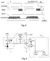
- FIG. 1is a symbol circuit diagram illustrating the electrical circuit of a first embodiment of an active pixel according to the present invention.
- FIG. 2is a symbol circuit diagram illustrating the electrical circuit of a second embodiment of an active pixel according to the present invention.
- FIG. 3is a timing chart of the different signals in the electrical circuit of the active pixel of FIG. 1 .
- FIG. 4is a schematic circuit diagram illustrating a most simple embodiment-of an active pixel according to the present invention.
- FIGS. 1 and 4principally depict in schematic form an active pixel according to the present invention, FIG. 4 illustrating the most simple embodiment, and FIG. 1 illustrating a more elaborate embodiment.
- the input signal to an active pixelis the radiation intensity at the location of that pixel.
- the radiationmay be any of optical light, IR light, UV light, high energy particles, X-rays, etc.
- the incident light intensityis transduced by a photodiode (the sensor) and its associated circuits to an analog voltage at the output of the pixel.
- the sensingis done via a sensor circuit 1 , comprising a reverse-biased photodiode D and a reset transistor M 1 .
- the photodiode Dis reset periodically to a fixed bias by means of reset transistor M 1 , which is coupled between the reverse-biased photodiode D and a (positive) power supply VDD.
- Transistor M 1pre-charges the junction capacitance of the photodiode D at the beginning of every integration period when a reset signal is applied to the gate G 1 of the reset transistor M 1 .
- the photodiode Dcollects photogenerated charges, e.g. electrons (a semiconductor silicon substrate exposed to photons results in a release of charge carriers) and discharges in proportion to the integration period and the photocurrent of the photodiode D.
- the current that the photons of the light generate in the photodiode Dis related to the incident light directly. For a linear device the current generated is preferably proportional to the light intensity.
- the connection between the reset transistor M 1 and the photodiode Dis the photodiode node P.
- the photodiode node Pis directly coupled to a first terminal of a memory circuit 3 , comprising a memory capacitor C 1 .
- a signal integrated in the photodiodeis present on the memory capacitor C 1 .
- the signal present on the capacitor C 1can be consequently sensed by a buffer 6 , for example comprising buffer transistor M 5 , and read out in a conventional line-addressing/column readout fashion by the transistor M 6 .
- the combination of transistors M 5 and M 6is only one possible implementation of a buffer/multiplexer. Many other schemes are possible for that part, and are known to a person skilled in the art.
- the second terminal of the capacitor C 1is clocked by a pulsed signal VMEM, in order to compensate for threshold voltage losses in other parts of the circuit.
- the pulsed signal VMEMmay be provided by a timing circuit.
- the gate G 2 of transistor M 2is connected to the photodiode node P, where a voltage signal corresponding to the collected charge on the photodiode D is generated.
- Transistor M 2acts as a buffer circuit 7 .
- the drain D 2 of transistor M 2is connected to the positive power supply VDD, and its source S 2 is connected to an input of a sample circuit 2 .
- At the source S 2 of buffer transistor M 2appears a voltage that is a measure for the charge on the photodiode node P.
- the signal at source S 2 of buffer transistor M 2is sampled by the sample circuit 2 , and transferred to the memory circuit 3 , comprising a memory capacitor C 1 as represented in FIG.
- Sample circuit 2 and memory circuit 3together act as a sample and hold stage for the signal at the source S 2 of transistor M 2 .
- Closing the switch formed by sample transistor M 3by applying a sample signal to the gate G 3 of the sample transistor M 3 , freezes the signal voltage on the capacitor C 1 .
- the voltage on the capacitor C 1depends on the transfer function of the sample unit.
- the sample unitcan either be a voltage follower buffer or a switch that transfers some of the charge stored in the photodiode depletion capacitance into the memory capacitor C 1 .
- FIG. 1represents a voltage follower (source follower M 2 ) plus switch (M 3 ).
- Pre-charge circuit 5comprising transistor M 4 serves to pre-charge the voltage on the capacitor C 1 to a low level upon application of a pre-charge pulse to the gate G 4 of this transistor M 4 , the source of the pre-charge transistor M 4 being tied to the ground.
- the voltage frozen on the capacitor C 1can be consequently sensed by a buffer 6 , for example comprising buffer transistor M 5 , and read out in a conventional line-addressing/column readout fashion by the transistor M 6 .
- transistors M 5 and M 6are only one possible implementation of a buffer/multiplexer. Many other schemes are possible for that part, and are known to a person skilled in the art. All control signals necessary to implement the above embodiments may be generated by a dedicated timing circuit.
- the readingmay occur several times during the sensing of a new value, while the sample and reset switches (respectively transistors M 3 and M 1 ) are off.
- the line selection switch M 6closes, and the voltage at the source S 5 of buffer transistor M 5 is transferred to the column bus.
- the column output linemay end in a current load or a resistive load and will forward the pixel signal to a columns amplifier or another type of amplifier (whereby the type is not relevant for the present invention).
- a timing chart thereofis shown in FIG. 3 .
- a reset signal, applied to the gate G 1 of transistor M 1discharges the photodiode node P, in order to start a new integration period.
- a precharge signal, applied to the gate G 4 of the pre-charge transistor M 4pre-charges the memory capacitor C 1 to a low level.
- a pre-charge pulseshould occur before a sample switch pulse occurs at the gate G 3 of a sample transistor M 3 .
- the sample switch pulsecharges the memory capacitor C 1 to the signal level present at the source S 2 of the buffer transistor M 2 .
- a line-selection signal applied at the gate G 6 of the transistor M 6selects a particular line (or row) of pixels for readout.
- the line-selection signalcan be applied at any moment between two sample pulses. This is illustrated by the hatched zones, which show where a pulse can be.
- the pulses reset, sample and prechargemay be specific for each pixel individually, or common for rows of pixels. A special case is where these three signals are common for all pixels in an image sensor.
- the effective integration time of a pixelis the time between the opening of the reset switch transistor M 1 and the opening of the sample and hold switch transistor M 3 , the time when the pixels “see” can be fixed independently of the moment of readout of the pixels, which is determined by the line-selection signal applied to the readout transistor M 6 .
- the second terminal of the capacitor C 1is clocked by a pulsed signal VMEM. All the above signals may be provided by a dedicated timing circuit, especially those timing signals shown in or derivable from FIG. 3 .
- the signal on the gate G 2 of transistor M 2is at least a threshold voltage VTH below the positive power supply level VDD of the circuit, or lower.
- the signal on the source S 2 of M 2is another threshold voltage VTH under the signal on the gate G 2 of transistor M 2 , thus least 2 times VTH below the VDD level of the circuit, or lower.
- the signal on the drain D 4 of pre-charge transistor M 4 and on the capacitor C 1is 2 times VTH below VDD, or even lower.
- Another threshold voltage dropoccurs in buffer transistor M 5 . In view of modern CMOS processes, with low power supply voltages (3.3 V, 2.5 V, . . . ) the signal range is thereby greatly reduced.
- the pulsed signal VMEM applied to the second terminal of capacitor C 1is applied at a low voltage.
- the first terminal of the capacitor C 1is pre-charged by the pre-charge circuit 5 , and subsequently the pixel signal is sampled and held on that node.
- This signalhas at least 2 VTH losses compared to VDD.
- the sample and hold switch M 3is opened again.
- the voltage VMEM applied to the second terminal of the capacitor C 1is raised. Consequently the signal on the capacitor C 1 will rise along with it. The amplitude of this rise will determine the rise of signal voltage, so that these can be compensated for the VTH losses in the other parts of the circuit.
- the timing of the VMEM signalis shown in FIG. 3 : it may go low before or after the pre-charge pulse (as shown by the hatched zone), but in any case before the sample pulse, and it goes high again after the sample pulse. All the above signals may be provided by a timing circuit.
- Correlated double samplingis a technique of taking two samples of a signal closely spaced in time and subtracting the first signal from the second to remove low-frequency noise. Sampling of the pixel output occurs twice: once after reset and once after integrating the signal charge. The subtraction removes the reset noise (kTC noise) and dc offset from the signal charge.
- a pixelFor correlated double sampling, a pixel needs to be able to yield, just after each other, the reset voltage on a capacitance, and the signal voltage on the same capacitance after it has integrated charge. Consecutive electronic circuitry (which is straightforward for persons skilled in the art) subtracts these two voltages and yields a more offset-free and noise-free result. With the present pixel structure this can be realised as the memory capacitor allows memorising of the reset level on the photodiode. At the moment of readout of the pixels, this reset voltage can be read, and by switching the pre-charge transistor and the sample transistor, the actual signal voltage, possibly also memorised, can be read immediately after it. All necessary control signals can be provided by a timing circuit.
- FIG. 2shows a second embodiment of the pixel, where the source S 4 of the “precharge” transistor is connected to the column output and not to ground. This saves the use of a ground connection in each pixel, saving silicon area and making the pixel less opaque. Other details of this embodiment are the same as for the first embodiment.
Landscapes
- Engineering & Computer Science (AREA)
- Multimedia (AREA)
- Signal Processing (AREA)
- Transforming Light Signals Into Electric Signals (AREA)
- Solid State Image Pick-Up Elements (AREA)
Abstract
Description
Claims (24)
Priority Applications (2)
| Application Number | Priority Date | Filing Date | Title |
|---|---|---|---|
| US09/906,418US7224389B2 (en) | 2001-07-16 | 2001-07-16 | Method to adjust the signal level of an active pixel and corresponding active pixel |
| DE10231082ADE10231082A1 (en) | 2001-07-16 | 2002-07-10 | Method for setting a signal level of an active picture element and corresponding active picture element |
Applications Claiming Priority (1)
| Application Number | Priority Date | Filing Date | Title |
|---|---|---|---|
| US09/906,418US7224389B2 (en) | 2001-07-16 | 2001-07-16 | Method to adjust the signal level of an active pixel and corresponding active pixel |
Publications (2)
| Publication Number | Publication Date |
|---|---|
| US20030011694A1 US20030011694A1 (en) | 2003-01-16 |
| US7224389B2true US7224389B2 (en) | 2007-05-29 |
Family
ID=25422416
Family Applications (1)
| Application Number | Title | Priority Date | Filing Date |
|---|---|---|---|
| US09/906,418Expired - LifetimeUS7224389B2 (en) | 2001-07-16 | 2001-07-16 | Method to adjust the signal level of an active pixel and corresponding active pixel |
Country Status (2)
| Country | Link |
|---|---|
| US (1) | US7224389B2 (en) |
| DE (1) | DE10231082A1 (en) |
Cited By (18)
| Publication number | Priority date | Publication date | Assignee | Title |
|---|---|---|---|---|
| US20050024510A1 (en)* | 2003-02-17 | 2005-02-03 | Silverbrook Research Pty Ltd | Image sensor with digital frame store |
| US20060044438A1 (en)* | 2004-08-25 | 2006-03-02 | Mauritzson Richard A | Pixel for boosting pixel reset voltage |
| US20060119720A1 (en)* | 2004-12-03 | 2006-06-08 | Micron Technology, Inc. | Imager pixel with capacitance circuit for boosting reset voltage |
| US20060285000A1 (en)* | 2003-09-10 | 2006-12-21 | Keiji Mabuchi | Semiconductor device, and control method and device for driving unit component of semiconductor device |
| US20090141155A1 (en)* | 2007-11-30 | 2009-06-04 | International Business Machines Corporation | High dynamic range imaging cell with electronic shutter extensions |
| US20090230289A1 (en)* | 2006-11-29 | 2009-09-17 | Cypress Semiconductor Corporation | Pixel Structure Having Shielded Storage Node |
| EP2109306A2 (en) | 2008-04-07 | 2009-10-14 | CMOSIS nv | Pixel array with global shutter |
| US20100014784A1 (en)* | 1999-09-17 | 2010-01-21 | Silverbrook Research Pty Ltd. | Sensing Device For Subsampling Imaged Coded Data |
| US20100072350A1 (en)* | 2008-09-22 | 2010-03-25 | Cypress Semiconductor Corporation | Active pixel with precharging circuit |
| US20100079632A1 (en)* | 2008-09-26 | 2010-04-01 | Tom Walschap | Correlated double sampling pixel |
| US7719590B2 (en)* | 2007-03-16 | 2010-05-18 | International Business Machines Corporation | High dynamic range imaging cell with electronic shutter extensions |
| US20110058082A1 (en)* | 2001-11-06 | 2011-03-10 | Hiok Nam Tay | CMOS Image Sensor with Noise Cancellation |
| US20120181589A1 (en)* | 2009-10-20 | 2012-07-19 | Semiconductor Manufacturing International (Shanghai) Corporation | Cmos image sensor with non-contact structure |
| US20120312967A1 (en)* | 2011-06-10 | 2012-12-13 | Yannick De Wit | Pixel and method |
| TWI683300B (en)* | 2018-08-29 | 2020-01-21 | 恆景科技股份有限公司 | Pixel circuit |
| US11317050B2 (en) | 2005-03-11 | 2022-04-26 | Hand Held Products, Inc. | Image reader comprising CMOS based image sensor array |
| US11394910B2 (en)* | 2016-01-19 | 2022-07-19 | SK Hynix Inc. | Image sensing device generating pixel signal with boost voltage and operating method thereof |
| US11604933B2 (en) | 2005-06-03 | 2023-03-14 | Hand Held Products, Inc. | Apparatus having hybrid monochrome and color image sensor array |
Families Citing this family (17)
| Publication number | Priority date | Publication date | Assignee | Title |
|---|---|---|---|---|
| US7019277B2 (en)* | 2003-03-13 | 2006-03-28 | Psion Teklogix Systems Inc. | Imaging device |
| GB0411648D0 (en)* | 2004-05-25 | 2004-06-30 | Fillfactory N V | Method and pixel for performing correlated double sampling |
| US7750958B1 (en) | 2005-03-28 | 2010-07-06 | Cypress Semiconductor Corporation | Pixel structure |
| US7808022B1 (en) | 2005-03-28 | 2010-10-05 | Cypress Semiconductor Corporation | Cross talk reduction |
| US7411168B2 (en)* | 2005-07-28 | 2008-08-12 | Imagerlaes, Inc. | CMOS imager with wide dynamic range pixel |
| GB2439118A (en)* | 2006-06-12 | 2007-12-19 | Sharp Kk | Image sensor and display |
| GB2439098A (en)* | 2006-06-12 | 2007-12-19 | Sharp Kk | Image sensor and display |
| KR101279596B1 (en)* | 2006-09-18 | 2013-06-28 | 삼성디스플레이 주식회사 | Array substrate and display apparatus having the same |
| US7674648B2 (en)* | 2007-03-21 | 2010-03-09 | Eastman Kodak Company | Extended dynamic range using variable sensitivity pixels |
| US8045028B1 (en) | 2007-04-23 | 2011-10-25 | On Semiconductor Trading Ltd. | Six transistor (6T) pixel architecture |
| CN101779299B (en)* | 2007-08-21 | 2011-07-27 | 夏普株式会社 | Display device |
| US8546765B2 (en)* | 2008-06-26 | 2013-10-01 | Trixell | High dynamic range X-ray detector with improved signal to noise ratio |
| FR2941827B1 (en)* | 2009-01-30 | 2016-12-09 | Soc Francaise De Detecteurs Infrarouges - Sofradir | ACQUISITION CIRCUIT COMPRISING A BUFFER CAPACITOR |
| US9200954B2 (en) | 2011-11-07 | 2015-12-01 | The Johns Hopkins University | Flexible readout and signal processing in a computational sensor array |
| GB2539457A (en)* | 2015-06-16 | 2016-12-21 | Nordic Semiconductor Asa | Voltage regulators |
| CN106372269B (en)* | 2015-07-20 | 2020-10-20 | 复旦大学 | A radiation-resistant layout design method for memory cell circuits |
| CN110099229B (en)* | 2018-01-30 | 2023-04-28 | 松下知识产权经营株式会社 | camera device |
Citations (5)
| Publication number | Priority date | Publication date | Assignee | Title |
|---|---|---|---|---|
| US5128534A (en)* | 1990-07-17 | 1992-07-07 | Hughes Aircraft Company | High charge capacity focal plane array readout cell |
| US5461425A (en)* | 1994-02-15 | 1995-10-24 | Stanford University | CMOS image sensor with pixel level A/D conversion |
| US5990948A (en)* | 1996-02-29 | 1999-11-23 | Kabushiki Kaisha Toshiba | Noise cancelling circuit for pixel signals and an image pickup device using the noise cancelling circuit |
| US6166367A (en)* | 1998-03-26 | 2000-12-26 | Photobit Corporation | Programmable analog arithmetic circuit for imaging sensor |
| US6836291B1 (en)* | 1998-04-30 | 2004-12-28 | Minolta Co., Ltd. | Image pickup device with integral amplification |
- 2001
- 2001-07-16USUS09/906,418patent/US7224389B2/ennot_activeExpired - Lifetime
- 2002
- 2002-07-10DEDE10231082Apatent/DE10231082A1/ennot_activeCeased
Patent Citations (5)
| Publication number | Priority date | Publication date | Assignee | Title |
|---|---|---|---|---|
| US5128534A (en)* | 1990-07-17 | 1992-07-07 | Hughes Aircraft Company | High charge capacity focal plane array readout cell |
| US5461425A (en)* | 1994-02-15 | 1995-10-24 | Stanford University | CMOS image sensor with pixel level A/D conversion |
| US5990948A (en)* | 1996-02-29 | 1999-11-23 | Kabushiki Kaisha Toshiba | Noise cancelling circuit for pixel signals and an image pickup device using the noise cancelling circuit |
| US6166367A (en)* | 1998-03-26 | 2000-12-26 | Photobit Corporation | Programmable analog arithmetic circuit for imaging sensor |
| US6836291B1 (en)* | 1998-04-30 | 2004-12-28 | Minolta Co., Ltd. | Image pickup device with integral amplification |
Non-Patent Citations (1)
| Title |
|---|
| Yadid-Pecht, "A random access photodiode array for intelligent image capture", IEEE Transactions of Electron Devices, vol. 38, No. 8, Aug. 1991, p. 1772. |
Cited By (64)
| Publication number | Priority date | Publication date | Assignee | Title |
|---|---|---|---|---|
| US20100014784A1 (en)* | 1999-09-17 | 2010-01-21 | Silverbrook Research Pty Ltd. | Sensing Device For Subsampling Imaged Coded Data |
| US8416468B2 (en) | 1999-09-17 | 2013-04-09 | Silverbrook Research Pty Ltd | Sensing device for subsampling imaged coded data |
| US20110058082A1 (en)* | 2001-11-06 | 2011-03-10 | Hiok Nam Tay | CMOS Image Sensor with Noise Cancellation |
| US7760259B2 (en)* | 2003-02-17 | 2010-07-20 | Silverbrook Research Pty Ltd | Pixel sensor |
| US20100002111A1 (en)* | 2003-02-17 | 2010-01-07 | Silverbrook Research Pty Ltd | Photodetecting Circuit |
| US8023020B2 (en)* | 2003-02-17 | 2011-09-20 | Silverbrook Research Pty Ltd. | Pixel sensor with voltage compensator |
| US7990450B2 (en) | 2003-02-17 | 2011-08-02 | Silverbrook Research Pty Ltd | Photodetecting circuit |
| US7515186B2 (en)* | 2003-02-17 | 2009-04-07 | Silverbrook Research Pty Ltd | Pixel sensor |
| US20050024512A1 (en)* | 2003-02-17 | 2005-02-03 | Silverbrook Research Pty Ltd | Pixel sensor |
| US20090160986A1 (en)* | 2003-02-17 | 2009-06-25 | Silverbrook Research Pty Ltd | Pixel sensor |
| US20100302426A1 (en)* | 2003-02-17 | 2010-12-02 | Silverbrook Research Pty Ltd | Pixel sensor with voltage compensator |
| US20050024510A1 (en)* | 2003-02-17 | 2005-02-03 | Silverbrook Research Pty Ltd | Image sensor with digital frame store |
| US7511275B2 (en)* | 2003-09-10 | 2009-03-31 | Sony Corporation | Semiconductor device, and control method and device for driving unit component of semiconductor device |
| US20060285000A1 (en)* | 2003-09-10 | 2006-12-21 | Keiji Mabuchi | Semiconductor device, and control method and device for driving unit component of semiconductor device |
| US7652704B2 (en)* | 2004-08-25 | 2010-01-26 | Aptina Imaging Corporation | Pixel for boosting pixel reset voltage |
| US8026969B2 (en) | 2004-08-25 | 2011-09-27 | Aptina Imaging Corporation | Pixel for boosting pixel reset voltage |
| US20100097509A1 (en)* | 2004-08-25 | 2010-04-22 | Mauritzson Richard A | Pixel for boosting pixel reset voltage |
| US20060044438A1 (en)* | 2004-08-25 | 2006-03-02 | Mauritzson Richard A | Pixel for boosting pixel reset voltage |
| US7777169B2 (en) | 2004-12-03 | 2010-08-17 | Aptina Imaging Corporation | Imager pixel with capacitance circuit for boosting reset voltage |
| US7446807B2 (en)* | 2004-12-03 | 2008-11-04 | Micron Technology, Inc. | Imager pixel with capacitance for boosting reset voltage |
| US20060119720A1 (en)* | 2004-12-03 | 2006-06-08 | Micron Technology, Inc. | Imager pixel with capacitance circuit for boosting reset voltage |
| US20090001255A1 (en)* | 2004-12-03 | 2009-01-01 | Hong Sungkwon C | Imager pixel with capacitance circuit for boosting reset voltage |
| US11323649B2 (en) | 2005-03-11 | 2022-05-03 | Hand Held Products, Inc. | Image reader comprising CMOS based image sensor array |
| US12075176B2 (en) | 2005-03-11 | 2024-08-27 | Hand Held Products, Inc. | Image reader comprising CMOS based image sensor array |
| US12185006B2 (en) | 2005-03-11 | 2024-12-31 | Hand Held Products, Inc. | Image reader comprising CMOS based image sensor array |
| US11317050B2 (en) | 2005-03-11 | 2022-04-26 | Hand Held Products, Inc. | Image reader comprising CMOS based image sensor array |
| US11323650B2 (en) | 2005-03-11 | 2022-05-03 | Hand Held Products, Inc. | Image reader comprising CMOS based image sensor array |
| US11968464B2 (en) | 2005-03-11 | 2024-04-23 | Hand Held Products, Inc. | Image reader comprising CMOS based image sensor array |
| US11863897B2 (en) | 2005-03-11 | 2024-01-02 | Hand Held Products, Inc. | Image reader comprising CMOS based image sensor array |
| US11604933B2 (en) | 2005-06-03 | 2023-03-14 | Hand Held Products, Inc. | Apparatus having hybrid monochrome and color image sensor array |
| US11625550B2 (en) | 2005-06-03 | 2023-04-11 | Hand Held Products, Inc. | Apparatus having hybrid monochrome and color image sensor array |
| US12321814B2 (en) | 2005-06-03 | 2025-06-03 | Hand Held Products, Inc. | Apparatus having hybrid monochrome and color image sensor array |
| US12321815B2 (en) | 2005-06-03 | 2025-06-03 | Hand Held Products, Inc. | Apparatus having hybrid monochrome and color image sensor array |
| US12321813B2 (en) | 2005-06-03 | 2025-06-03 | Hand Held Products, Inc. | Apparatus having hybrid monochrome and color image sensor array |
| US12236312B2 (en) | 2005-06-03 | 2025-02-25 | Hand Held Products, Inc. | Apparatus having hybrid monochrome and color image sensor array |
| US12073283B2 (en) | 2005-06-03 | 2024-08-27 | Hand Held Products, Inc. | Apparatus having hybrid monochrome and color image sensor array |
| US12026580B2 (en) | 2005-06-03 | 2024-07-02 | Hand Held Products, Inc. | Apparatus having hybrid monochrome and color image sensor array |
| US12020111B2 (en) | 2005-06-03 | 2024-06-25 | Hand Held Products, Inc. | Apparatus having hybrid monochrome and color image sensor array |
| US12001914B2 (en) | 2005-06-03 | 2024-06-04 | Hand Held Products, Inc. | Apparatus having hybrid monochrome and color image sensor array |
| US12001913B2 (en) | 2005-06-03 | 2024-06-04 | Hand Held Products, Inc. | Apparatus having hybrid monochrome and color image sensor array |
| US8207485B2 (en) | 2006-11-29 | 2012-06-26 | On Semiconductor Image Sensor | Pixel structure having shielded storage node |
| US20090230289A1 (en)* | 2006-11-29 | 2009-09-17 | Cypress Semiconductor Corporation | Pixel Structure Having Shielded Storage Node |
| US7719590B2 (en)* | 2007-03-16 | 2010-05-18 | International Business Machines Corporation | High dynamic range imaging cell with electronic shutter extensions |
| US7948535B2 (en) | 2007-11-30 | 2011-05-24 | International Business Machines Corporation | High dynamic range imaging cell with electronic shutter extensions |
| US20090141155A1 (en)* | 2007-11-30 | 2009-06-04 | International Business Machines Corporation | High dynamic range imaging cell with electronic shutter extensions |
| EP2109306A2 (en) | 2008-04-07 | 2009-10-14 | CMOSIS nv | Pixel array with global shutter |
| EP2109306A3 (en)* | 2008-04-07 | 2012-06-13 | CMOSIS nv | Pixel array with global shutter |
| US20090256060A1 (en)* | 2008-04-07 | 2009-10-15 | Guy Meynants | Pixel array with global shutter |
| US8754357B2 (en) | 2008-04-07 | 2014-06-17 | Cmosis Nv | Pixel having two cascade-connected sample stages, pixel array, and method of operating same |
| US8569671B2 (en) | 2008-04-07 | 2013-10-29 | Cmosis Nv | Pixel array capable of performing pipelined global shutter operation including a first and second buffer amplifier |
| US20100072350A1 (en)* | 2008-09-22 | 2010-03-25 | Cypress Semiconductor Corporation | Active pixel with precharging circuit |
| US8476567B2 (en) | 2008-09-22 | 2013-07-02 | Semiconductor Components Industries, Llc | Active pixel with precharging circuit |
| US20100079632A1 (en)* | 2008-09-26 | 2010-04-01 | Tom Walschap | Correlated double sampling pixel |
| US8059173B2 (en)* | 2008-09-26 | 2011-11-15 | On Semiconductor Trading Ltd. | Correlated double sampling pixel and method |
| US8513721B2 (en)* | 2009-10-20 | 2013-08-20 | Semiconductor Manufacturing International (Shanghai) Corporation | CMOS image sensor with non-contact structure |
| US20120181589A1 (en)* | 2009-10-20 | 2012-07-19 | Semiconductor Manufacturing International (Shanghai) Corporation | Cmos image sensor with non-contact structure |
| US20120312967A1 (en)* | 2011-06-10 | 2012-12-13 | Yannick De Wit | Pixel and method |
| US8987646B2 (en)* | 2011-06-10 | 2015-03-24 | Semiconductor Components Industries, Llc | Pixel and method |
| US11394910B2 (en)* | 2016-01-19 | 2022-07-19 | SK Hynix Inc. | Image sensing device generating pixel signal with boost voltage and operating method thereof |
| TWI683300B (en)* | 2018-08-29 | 2020-01-21 | 恆景科技股份有限公司 | Pixel circuit |
| US10791291B2 (en) | 2018-08-29 | 2020-09-29 | Himax Imaging Limited | Pixel circuit |
| US10917596B2 (en) | 2018-08-29 | 2021-02-09 | Himax Imaging Limited | Pixel circuit for generating output signals in response to incident radiation |
| US11128829B2 (en) | 2018-08-29 | 2021-09-21 | Himax Imaging Limited | Pixel circuit |
| US11172153B2 (en) | 2018-08-29 | 2021-11-09 | Himax Imaging Limited | Pixel circuit |
Also Published As
| Publication number | Publication date |
|---|---|
| DE10231082A1 (en) | 2003-02-06 |
| US20030011694A1 (en) | 2003-01-16 |
Similar Documents
| Publication | Publication Date | Title |
|---|---|---|
| US7224389B2 (en) | Method to adjust the signal level of an active pixel and corresponding active pixel | |
| US6380530B1 (en) | Method for operating a high sensitivity active pixel | |
| KR100660193B1 (en) | Self compensating correlated double sampling circuit | |
| US5898168A (en) | Image sensor pixel circuit | |
| US6917027B2 (en) | Method and apparatus for reducing kTC noise in an active pixel sensor (APS) device | |
| US5880460A (en) | Active pixel sensor cell that reduces noise in the photo information extracted from the cell | |
| US7375748B2 (en) | Differential readout from pixels in CMOS sensor | |
| JP2976242B2 (en) | Integrated circuit, camera using the integrated circuit, and method for detecting incident light incident on an image sensor manufactured using the integrated circuit technology | |
| US8059173B2 (en) | Correlated double sampling pixel and method | |
| JP4288346B2 (en) | Imaging device and pixel circuit | |
| EP2863627A1 (en) | An image sensor | |
| US4734776A (en) | Readout circuit for an optical sensing charge injection device facilitating an extended dynamic range | |
| US6157016A (en) | Fast CMOS active-pixel sensor array readout circuit with predischarge circuit | |
| US20060170491A1 (en) | Optoelectronic sensor | |
| CN113489923B (en) | Optical active pixel sensor using TFT pixel circuit | |
| US7973845B2 (en) | Method and pixel for performing correlated double sampling | |
| EP3714595B1 (en) | Pixel sensor cell for cmos image sensors with enhanced conversion gain at high dynamic range capability | |
| US4734583A (en) | Readout circuit for dual-gate CID imagers with charge sharing corrected for subtractive error | |
| US10700654B2 (en) | High dynamic range capacitor transimpedance amplifier | |
| JP2000209508A (en) | Solid-state imaging device | |
| US7652240B2 (en) | Image sensor with a plurality of pixels, pixel circuit and method | |
| JP2743842B2 (en) | Infrared detector | |
| US20060164107A1 (en) | Image sensor | |
| EP0928102B1 (en) | Array sensors | |
| GB2414548A (en) | Image sensor with correlated double sampling |
Legal Events
| Date | Code | Title | Description |
|---|---|---|---|
| AS | Assignment | Owner name:FILLFACTORY, BELGIUM Free format text:CHANGE OF NAME;ASSIGNOR:DIERICKX, BART;REEL/FRAME:012452/0130 Effective date:20011031 | |
| AS | Assignment | Owner name:CYPRESS SEMICONDUCTOR CORPORATION (BELGIUM) BVBA, Free format text:ASSIGNMENT OF ASSIGNORS INTEREST;ASSIGNOR:FILLFACTORY N.V.;REEL/FRAME:017094/0208 Effective date:20040621 | |
| STCF | Information on status: patent grant | Free format text:PATENTED CASE | |
| FEPP | Fee payment procedure | Free format text:PAYOR NUMBER ASSIGNED (ORIGINAL EVENT CODE: ASPN); ENTITY STATUS OF PATENT OWNER: LARGE ENTITY Free format text:PAYER NUMBER DE-ASSIGNED (ORIGINAL EVENT CODE: RMPN); ENTITY STATUS OF PATENT OWNER: LARGE ENTITY | |
| FPAY | Fee payment | Year of fee payment:4 | |
| AS | Assignment | Owner name:ON SEMICONDUCTOR IMAGE SENSOR, BELGIUM Free format text:CHANGE OF NAME;ASSIGNOR:CYPRESS SEMICONDUCTOR CORPORATION (BELGIUM) BVBA;REEL/FRAME:026319/0730 Effective date:20110414 | |
| AS | Assignment | Owner name:SEMICONDUCTOR COMPONENTS INDUSTRIES, LLC, ARIZONA Free format text:ASSIGNMENT OF ASSIGNORS INTEREST;ASSIGNOR:ON SEMICONDUCTOR IMAGE SENSOR BVBA;REEL/FRAME:028598/0477 Effective date:20120629 | |
| FPAY | Fee payment | Year of fee payment:8 | |
| AS | Assignment | Owner name:DEUTSCHE BANK AG NEW YORK BRANCH, NEW YORK Free format text:SECURITY INTEREST;ASSIGNOR:SEMICONDUCTOR COMPONENTS INDUSTRIES, LLC;REEL/FRAME:038620/0087 Effective date:20160415 | |
| AS | Assignment | Owner name:DEUTSCHE BANK AG NEW YORK BRANCH, AS COLLATERAL AGENT, NEW YORK Free format text:CORRECTIVE ASSIGNMENT TO CORRECT THE INCORRECT PATENT NUMBER 5859768 AND TO RECITE COLLATERAL AGENT ROLE OF RECEIVING PARTY IN THE SECURITY INTEREST PREVIOUSLY RECORDED ON REEL 038620 FRAME 0087. ASSIGNOR(S) HEREBY CONFIRMS THE SECURITY INTEREST;ASSIGNOR:SEMICONDUCTOR COMPONENTS INDUSTRIES, LLC;REEL/FRAME:039853/0001 Effective date:20160415 Owner name:DEUTSCHE BANK AG NEW YORK BRANCH, AS COLLATERAL AG Free format text:CORRECTIVE ASSIGNMENT TO CORRECT THE INCORRECT PATENT NUMBER 5859768 AND TO RECITE COLLATERAL AGENT ROLE OF RECEIVING PARTY IN THE SECURITY INTEREST PREVIOUSLY RECORDED ON REEL 038620 FRAME 0087. ASSIGNOR(S) HEREBY CONFIRMS THE SECURITY INTEREST;ASSIGNOR:SEMICONDUCTOR COMPONENTS INDUSTRIES, LLC;REEL/FRAME:039853/0001 Effective date:20160415 | |
| MAFP | Maintenance fee payment | Free format text:PAYMENT OF MAINTENANCE FEE, 12TH YEAR, LARGE ENTITY (ORIGINAL EVENT CODE: M1553); ENTITY STATUS OF PATENT OWNER: LARGE ENTITY Year of fee payment:12 | |
| AS | Assignment | Owner name:FAIRCHILD SEMICONDUCTOR CORPORATION, ARIZONA Free format text:RELEASE OF SECURITY INTEREST IN PATENTS RECORDED AT REEL 038620, FRAME 0087;ASSIGNOR:DEUTSCHE BANK AG NEW YORK BRANCH, AS COLLATERAL AGENT;REEL/FRAME:064070/0001 Effective date:20230622 Owner name:SEMICONDUCTOR COMPONENTS INDUSTRIES, LLC, ARIZONA Free format text:RELEASE OF SECURITY INTEREST IN PATENTS RECORDED AT REEL 038620, FRAME 0087;ASSIGNOR:DEUTSCHE BANK AG NEW YORK BRANCH, AS COLLATERAL AGENT;REEL/FRAME:064070/0001 Effective date:20230622 |