US7223686B2 - Semiconductor interconnection line and method of forming the same - Google Patents
Semiconductor interconnection line and method of forming the sameDownload PDFInfo
- Publication number
- US7223686B2 US7223686B2US11/026,717US2671704AUS7223686B2US 7223686 B2US7223686 B2US 7223686B2US 2671704 AUS2671704 AUS 2671704AUS 7223686 B2US7223686 B2US 7223686B2
- Authority
- US
- United States
- Prior art keywords
- layer
- insulating layer
- interconnection line
- forming
- via hole
- Prior art date
- Legal status (The legal status is an assumption and is not a legal conclusion. Google has not performed a legal analysis and makes no representation as to the accuracy of the status listed.)
- Expired - Lifetime, expires
Links
Images


Classifications
- H—ELECTRICITY
- H01—ELECTRIC ELEMENTS
- H01L—SEMICONDUCTOR DEVICES NOT COVERED BY CLASS H10
- H01L21/00—Processes or apparatus adapted for the manufacture or treatment of semiconductor or solid state devices or of parts thereof
- H01L21/02—Manufacture or treatment of semiconductor devices or of parts thereof
- H01L21/04—Manufacture or treatment of semiconductor devices or of parts thereof the devices having potential barriers, e.g. a PN junction, depletion layer or carrier concentration layer
- H01L21/18—Manufacture or treatment of semiconductor devices or of parts thereof the devices having potential barriers, e.g. a PN junction, depletion layer or carrier concentration layer the devices having semiconductor bodies comprising elements of Group IV of the Periodic Table or AIIIBV compounds with or without impurities, e.g. doping materials
- H01L21/28—Manufacture of electrodes on semiconductor bodies using processes or apparatus not provided for in groups H01L21/20 - H01L21/268
- H—ELECTRICITY
- H01—ELECTRIC ELEMENTS
- H01L—SEMICONDUCTOR DEVICES NOT COVERED BY CLASS H10
- H01L21/00—Processes or apparatus adapted for the manufacture or treatment of semiconductor or solid state devices or of parts thereof
- H01L21/70—Manufacture or treatment of devices consisting of a plurality of solid state components formed in or on a common substrate or of parts thereof; Manufacture of integrated circuit devices or of parts thereof
- H01L21/71—Manufacture of specific parts of devices defined in group H01L21/70
- H01L21/768—Applying interconnections to be used for carrying current between separate components within a device comprising conductors and dielectrics
- H01L21/76801—Applying interconnections to be used for carrying current between separate components within a device comprising conductors and dielectrics characterised by the formation and the after-treatment of the dielectrics, e.g. smoothing
- H01L21/76802—Applying interconnections to be used for carrying current between separate components within a device comprising conductors and dielectrics characterised by the formation and the after-treatment of the dielectrics, e.g. smoothing by forming openings in dielectrics
- H01L21/76807—Applying interconnections to be used for carrying current between separate components within a device comprising conductors and dielectrics characterised by the formation and the after-treatment of the dielectrics, e.g. smoothing by forming openings in dielectrics for dual damascene structures
- H01L21/76808—Applying interconnections to be used for carrying current between separate components within a device comprising conductors and dielectrics characterised by the formation and the after-treatment of the dielectrics, e.g. smoothing by forming openings in dielectrics for dual damascene structures involving intermediate temporary filling with material
- H—ELECTRICITY
- H01—ELECTRIC ELEMENTS
- H01L—SEMICONDUCTOR DEVICES NOT COVERED BY CLASS H10
- H01L21/00—Processes or apparatus adapted for the manufacture or treatment of semiconductor or solid state devices or of parts thereof
- H01L21/70—Manufacture or treatment of devices consisting of a plurality of solid state components formed in or on a common substrate or of parts thereof; Manufacture of integrated circuit devices or of parts thereof
- H01L21/71—Manufacture of specific parts of devices defined in group H01L21/70
- H01L21/768—Applying interconnections to be used for carrying current between separate components within a device comprising conductors and dielectrics
- H01L21/76801—Applying interconnections to be used for carrying current between separate components within a device comprising conductors and dielectrics characterised by the formation and the after-treatment of the dielectrics, e.g. smoothing
- H01L21/76802—Applying interconnections to be used for carrying current between separate components within a device comprising conductors and dielectrics characterised by the formation and the after-treatment of the dielectrics, e.g. smoothing by forming openings in dielectrics
- H01L21/76807—Applying interconnections to be used for carrying current between separate components within a device comprising conductors and dielectrics characterised by the formation and the after-treatment of the dielectrics, e.g. smoothing by forming openings in dielectrics for dual damascene structures
- H—ELECTRICITY
- H01—ELECTRIC ELEMENTS
- H01L—SEMICONDUCTOR DEVICES NOT COVERED BY CLASS H10
- H01L21/00—Processes or apparatus adapted for the manufacture or treatment of semiconductor or solid state devices or of parts thereof
- H01L21/70—Manufacture or treatment of devices consisting of a plurality of solid state components formed in or on a common substrate or of parts thereof; Manufacture of integrated circuit devices or of parts thereof
- H01L21/71—Manufacture of specific parts of devices defined in group H01L21/70
- H01L21/768—Applying interconnections to be used for carrying current between separate components within a device comprising conductors and dielectrics
- H01L21/76838—Applying interconnections to be used for carrying current between separate components within a device comprising conductors and dielectrics characterised by the formation and the after-treatment of the conductors
- H01L21/76895—Local interconnects; Local pads, as exemplified by patent document EP0896365
- H—ELECTRICITY
- H01—ELECTRIC ELEMENTS
- H01L—SEMICONDUCTOR DEVICES NOT COVERED BY CLASS H10
- H01L21/00—Processes or apparatus adapted for the manufacture or treatment of semiconductor or solid state devices or of parts thereof
- H01L21/70—Manufacture or treatment of devices consisting of a plurality of solid state components formed in or on a common substrate or of parts thereof; Manufacture of integrated circuit devices or of parts thereof
- H01L21/71—Manufacture of specific parts of devices defined in group H01L21/70
- H01L21/768—Applying interconnections to be used for carrying current between separate components within a device comprising conductors and dielectrics
- H01L21/76801—Applying interconnections to be used for carrying current between separate components within a device comprising conductors and dielectrics characterised by the formation and the after-treatment of the dielectrics, e.g. smoothing
- H01L21/76829—Applying interconnections to be used for carrying current between separate components within a device comprising conductors and dielectrics characterised by the formation and the after-treatment of the dielectrics, e.g. smoothing characterised by the formation of thin functional dielectric layers, e.g. dielectric etch-stop, barrier, capping or liner layers
- H01L21/76834—Applying interconnections to be used for carrying current between separate components within a device comprising conductors and dielectrics characterised by the formation and the after-treatment of the dielectrics, e.g. smoothing characterised by the formation of thin functional dielectric layers, e.g. dielectric etch-stop, barrier, capping or liner layers formation of thin insulating films on the sidewalls or on top of conductors
Definitions
- the present disclosurerelates to a semiconductor device, and more particularly, to an interconnection line of a semiconductor device and a method of forming the same using a dual damascene process.
- Aluminum (Al)has mainly been used as an interconnection line material for a semiconductor device in the past.
- copper (Cu)has been recently used as an interconnection line material instead of Al, because the integration density and the speed of semiconductor devices have increased, so the line width of the interconnection lines has been reduced, thereby decreasing their resistance and contact resistance and reducing occurrence of electro migration (EM), is disclosed in U.S. Pat. No. 6,198,170.
- Cuhas low resistivity and high resistance against EM compared with Al, it can provide high reliability when used an interconnection line for a high integration density device and a high-speed device.
- a dual damascene processis used to form a via hole and a trench in an intermediate insulating layer, the via hole and the trench are filled with Cu, and a planarization process must be performed.
- FIG. 1AA known method of forming an interconnection line for a semiconductor device is described with reference to FIG. 1A to FIG. 1G .
- a semiconductor substrate 10 on which a lower insulating layer 11 and a first interconnection line 12 are formedis provided.
- An etch stop layer 13is then formed on the entire surface of the substrate, and an intermediate insulating layer 14 of an oxide layer is formed on the etch stop layer 13 .
- a first photoresist pattern(not shown) is formed on the intermediate insulating layer 14 by a photolithography process, and the intermediate insulating layer 14 is then etched by an etching process using the first photoresist pattern as an etching mask, to form a via hole 15 exposing the portion of the etch stop layer 13 over the first interconnection line 12 . Thereafter, the first photoresist pattern is removed by a well-known method.
- a sacrificial layer 16is formed on the intermediate insulating layer 14 to fill the via hole 15 .
- the sacrificial layer 16is then removed to expose the intermediate insulating layer and to form a recess over the sacrificial layer 16 of the via hole 15 .
- the sacrificial layer 16is formed of a photoresist layer.
- a second photoresist pattern 17is formed on the intermediate insulating layer 14 by a photolithography process, and the portion of the intermediate insulating layer 14 is then etched by an etching process using the second photoresist pattern 17 as an etch mask, to form a trench 18 including the via hole 15 at the upper portion of the via hole 15 .
- the second photoresist pattern 17is removed by a well-known method.
- the sacrificial layer 16is also removed, to expose the etch stop layer 13 at the bottom of the via hole 15 .
- the exposed portion of the etch stop layer 13is removed, to expose the first interconnection layer 12 at the bottom of the via hole 15 .
- a Cu layeris formed on the intermediate insulating layer 14 to fill the via hole 15 and the trench 18 , and a planarization process is then performed to expose the intermediate insulating layer 14 , thereby forming a second interconnection line 19 that is electrically connected to the first interconnection line 12 .
- the etch stop layer 13stops the intermediate insulating layer 14 from being etched to prevent damage to the first interconnection line 12 due to the etching. Therefore, a material having high etch selectivity to the intermediate insulating layer 14 such as, for example, a nitride layer must be used as the etch stop layer 13 .
- the nitride layerhas problems in that RC delay increases and the speed of a device manufactured thereby is deteriorated because it has a relatively high dielectric constant (high-k) compared with the oxide layer.
- an insulating layer of a low dielectric constant (low-k)has been used as the intermediate insulating layer 14 , but it is difficult to obtain good effects if the etch stop layer 13 at the bottom of the via hole 15 is not fully removed.
- the etch stop layer 13remains at the bottom of the via hole 15 because a polymer (not shown) remains over the sacrificial layer 16 when etching the intermediate insulating layer 14 for forming the trench 18 , and this prevents the sacrificial layer 16 from being removed when removing the second photoresist pattern 17 for the sacrificial layer 16 to remain in the via hole 15 , so that the etch stop layer 13 is not fully removed when removing the etch stop layer 13 .
- the sacrificial layer 16 remaining in the via hole 15must be fully removed by additionally performing a washing or a post etch treatment (PET), but there is problem in that this causes process time and fabrication cost to increase.
- PETpost etch treatment
- FIGS. 1A to 1Gare cross-sectional views depicting a known method of forming an interconnection line for a semiconductor device.
- FIGS. 2A to 2Fare cross-sectional views depicting an example method of forming an interconnection line for a semiconductor device.
- the example methods and apparatus described hereinprovide an interconnection line of a semiconductor device that is capable of preventing a lower interconnection line from being damaged when etching an intermediate insulating layer for forming a via hole and a trench, and reducing RC delay.
- the example interconnection line disclosed hereinincludes: a semiconductor substrate; a first interconnection line formed on the substrate; an insulating layer pattern formed on the substrate to expose the portion of the first interconnection line; a metal pad layer formed on the exposed portion of the first interconnection line; an intermediate insulating layer formed on the entire surface of the substrate and having a via hole and a trench exposing the metal pad layer; and a second interconnection formed in the via hole and the trench and electrically connected to the first interconnection line through the metal pad layer.
- An example method of forming the interconnection line for a semiconductor device described hereinincludes: providing a semiconductor substrate on which a first interconnection line is formed; forming an insulating layer pattern exposing a portion of the first interconnection line on the substrate; forming a metal pad layer on the exposed portion of the first interconnection line; forming an intermediate insulating layer on the entire surface of the substrate; etching the intermediate insulating layer to form a via hole exposing the metal pad layer; etching a portion of the intermediate insulating layer to form a trench at the upper portion of the via hole; and forming a second interconnection line electrically connected to the first interconnection line through the metal pad layer in the via hole and the trench.
- the insulating layer pattern and the intermediate insulating layerare respectively formed of one selected from a silicon oxide (SiO2) layer, an FSG (Fluoro-Silicate Glass) layer, and an insulating layer of a low dielectric constant (low-k) of below 3.0.
- the metal pad layeris formed of one selected from a W layer, a Ti layer, a TiN layer, a Ta layer and a TaN layer.
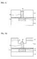
- FIG. 2AAn example method of forming an interconnection line for a semiconductor device is described with reference to FIG. 2A to FIG. 2F .
- a semiconductor substrate 20 on which a lower insulating layer 21 and a first interconnection line 22 are formedis provided.
- the first interconnection line 22is formed of a Cu layer.
- an insulating layer 23is relatively thinly formed on the entire surface of the substrate, and a first photoresist pattern 24 exposing the portion of the insulating layer 23 over the first interconnection line 22 is formed on the insulating layer 23 by a photolithography process.
- the insulating layer 23is formed of one selected from a silicon oxide (SiO2) layer, an FSG (Fluoro-Silicate Glass) layer, and an insulating layer of a low dielectric constant (low-k) of below 3.0. Furthermore, the first photoresist pattern 24 is thinly formed to provide as accurate an alignment as possible.
- the insulating layer 23is etched by an etching process using a first photoresist pattern 24 (referring to FIG. 2A ) as an etch mask to form an insulating pattern 23 a exposing the portion of the first interconnection line 22 .
- a first photoresist pattern 24(referring to FIG. 2A ) as an etch mask to form an insulating pattern 23 a exposing the portion of the first interconnection line 22 .
- the surface area of the first interconnection line 21 exposed by the insulating pattern 23 ais as large as possible.
- the first photoresist pattern 24is removed by a well-known method.
- a metal pad layer 25is selectively formed on the exposed portion of the first interconnection line 22 by a selective deposition method.
- the metal pad layer 24is formed of one selected from a W layer, a Ti layer, a TiN layer, a Ta layer and a TaN layer.
- the metal pad layer 25is formed to have as large a surface area, within a range in which a short-circuit with adjacent conductive layers (not shown) does not occur, as possible.
- an intermediate insulating layer 26is formed on the entire surface of the substrate to cover the insulating layer pattern 23 a and the metal pad layer 25 .
- the intermediate insulating layer 26is formed of one selected from a silicon oxide (SiO2) layer, an FSG (Fluoro-Silicate Glass) layer and an insulating layer of a low dielectric constant (low-k) of below 3.0 the same as the insulating layer 23 .
- a second photoresist pattern(not shown) is formed on the intermediate insulating layer 23 by a photolithography process, and the intermediate insulating layer 26 is etched by an etching process using the second photoresist pattern as an etch mask to form a via hole 27 exposing the metal pad layer 25 .
- the first interconnection line 22is protected by the metal pad layer 25 so that damage due to the etching does not occur at the first interconnection line 22 .
- the second photoresist patternis then removed by a well-known method.
- a third photoresist pattern(not shown) is formed on the intermediate insulating layer 26 by a photolithography process, and the portion of the intermediate insulating layer 26 is etched by an etching process using the third photoresist pattern as an etch mask, to form a trench 28 including the via hole 27 at the upper portion of the via hole 27 .
- the first interconnection line 22is also protected by the metal pad layer 25 so that damage due to the etching does not occur at the first interconnection line 22 .
- the third photoresist patternis then removed by a well-known method.
- a Cu layeris formed on the intermediate insulating layer 26 by an electroless plating method or an electroplating method so as to fill the via hole 27 and the trench 28 .
- a planarization processis performed by a chemical mechanical polishing (CMP) to expose the intermediate insulating layer 26 , thereby forming a second interconnection line 29 that is electrically connected to the first interconnection layer 22 through the metal pad layer 25 .
- CMPchemical mechanical polishing
- the metal pad layeris selectively formed on the first interconnection line and then the etching process for forming the via hole and the trench are respectively performed.
- the above-described methodcan reduce RC delay owing to forming the intermediate insulating layer and the insulating layer pattern with the insulating layer of a low dielectric constant (low-k) and can improve the yield and the reliability of a manufactured device.
Landscapes
- Engineering & Computer Science (AREA)
- Physics & Mathematics (AREA)
- Condensed Matter Physics & Semiconductors (AREA)
- General Physics & Mathematics (AREA)
- Manufacturing & Machinery (AREA)
- Computer Hardware Design (AREA)
- Microelectronics & Electronic Packaging (AREA)
- Power Engineering (AREA)
- Internal Circuitry In Semiconductor Integrated Circuit Devices (AREA)
Abstract
Description
Claims (9)
Priority Applications (1)
| Application Number | Priority Date | Filing Date | Title |
|---|---|---|---|
| US11/788,794US7960839B2 (en) | 2003-12-31 | 2007-04-20 | Semiconductor interconnection line and method of forming the same |
Applications Claiming Priority (2)
| Application Number | Priority Date | Filing Date | Title |
|---|---|---|---|
| KR10-2003-0101806 | 2003-12-31 | ||
| KR1020030101806AKR100552815B1 (en) | 2003-12-31 | 2003-12-31 | Dual damascene wiring formation method of semiconductor device |
Related Child Applications (1)
| Application Number | Title | Priority Date | Filing Date |
|---|---|---|---|
| US11/788,794DivisionUS7960839B2 (en) | 2003-12-31 | 2007-04-20 | Semiconductor interconnection line and method of forming the same |
Publications (2)
| Publication Number | Publication Date |
|---|---|
| US20050140020A1 US20050140020A1 (en) | 2005-06-30 |
| US7223686B2true US7223686B2 (en) | 2007-05-29 |
Family
ID=34698913
Family Applications (2)
| Application Number | Title | Priority Date | Filing Date |
|---|---|---|---|
| US11/026,717Expired - LifetimeUS7223686B2 (en) | 2003-12-31 | 2004-12-30 | Semiconductor interconnection line and method of forming the same |
| US11/788,794Active2028-02-04US7960839B2 (en) | 2003-12-31 | 2007-04-20 | Semiconductor interconnection line and method of forming the same |
Family Applications After (1)
| Application Number | Title | Priority Date | Filing Date |
|---|---|---|---|
| US11/788,794Active2028-02-04US7960839B2 (en) | 2003-12-31 | 2007-04-20 | Semiconductor interconnection line and method of forming the same |
Country Status (2)
| Country | Link |
|---|---|
| US (2) | US7223686B2 (en) |
| KR (1) | KR100552815B1 (en) |
Cited By (3)
| Publication number | Priority date | Publication date | Assignee | Title |
|---|---|---|---|---|
| US20070174633A1 (en)* | 2004-12-07 | 2007-07-26 | Draper Stark C | Biometric Based User Authentication and Data Encryption |
| US20070194448A1 (en)* | 2003-12-31 | 2007-08-23 | Se-Yeul Bae | Semiconductor interconnection line and method of forming the same |
| US20100299727A1 (en)* | 2008-11-18 | 2010-11-25 | Workshare Technology, Inc. | Methods and systems for exact data match filtering |
Families Citing this family (3)
| Publication number | Priority date | Publication date | Assignee | Title |
|---|---|---|---|---|
| KR100643853B1 (en)* | 2005-06-04 | 2006-11-14 | 삼성전자주식회사 | Method for forming damascene wiring of semiconductor device and semiconductor device manufactured thereby |
| KR100669851B1 (en)* | 2005-07-12 | 2007-01-16 | 삼성전자주식회사 | Manufacturing Method of Phase Change Memory Device |
| US11948874B2 (en)* | 2020-06-26 | 2024-04-02 | Intel Corporation | Vertically spaced intra-level interconnect line metallization for integrated circuit devices |
Citations (3)
| Publication number | Priority date | Publication date | Assignee | Title |
|---|---|---|---|---|
| US6084304A (en)* | 1998-05-01 | 2000-07-04 | United Microelectronics Corp. | Structure of metallization |
| US6559548B1 (en)* | 1999-03-19 | 2003-05-06 | Kabushiki Kaisha Toshiba | Wiring structure of semiconductor device |
| US6747355B2 (en)* | 2001-07-17 | 2004-06-08 | Nec Electronics Corporation | Semiconductor device and method for manufacturing the same |
Family Cites Families (4)
| Publication number | Priority date | Publication date | Assignee | Title |
|---|---|---|---|---|
| US5939788A (en)* | 1998-03-11 | 1999-08-17 | Micron Technology, Inc. | Copper diffusion barrier, aluminum wetting layer and improved methods for filling openings in silicon substrates with cooper |
| JP4425432B2 (en)* | 2000-06-20 | 2010-03-03 | Necエレクトロニクス株式会社 | Manufacturing method of semiconductor device |
| US7056820B2 (en)* | 2003-11-20 | 2006-06-06 | International Business Machines Corporation | Bond pad |
| KR100552815B1 (en)* | 2003-12-31 | 2006-02-22 | 동부아남반도체 주식회사 | Dual damascene wiring formation method of semiconductor device |
- 2003
- 2003-12-31KRKR1020030101806Apatent/KR100552815B1/ennot_activeExpired - Fee Related
- 2004
- 2004-12-30USUS11/026,717patent/US7223686B2/ennot_activeExpired - Lifetime
- 2007
- 2007-04-20USUS11/788,794patent/US7960839B2/enactiveActive
Patent Citations (3)
| Publication number | Priority date | Publication date | Assignee | Title |
|---|---|---|---|---|
| US6084304A (en)* | 1998-05-01 | 2000-07-04 | United Microelectronics Corp. | Structure of metallization |
| US6559548B1 (en)* | 1999-03-19 | 2003-05-06 | Kabushiki Kaisha Toshiba | Wiring structure of semiconductor device |
| US6747355B2 (en)* | 2001-07-17 | 2004-06-08 | Nec Electronics Corporation | Semiconductor device and method for manufacturing the same |
Cited By (5)
| Publication number | Priority date | Publication date | Assignee | Title |
|---|---|---|---|---|
| US20070194448A1 (en)* | 2003-12-31 | 2007-08-23 | Se-Yeul Bae | Semiconductor interconnection line and method of forming the same |
| US7960839B2 (en)* | 2003-12-31 | 2011-06-14 | Dongbu Electronics Co., Ltd. | Semiconductor interconnection line and method of forming the same |
| US20070174633A1 (en)* | 2004-12-07 | 2007-07-26 | Draper Stark C | Biometric Based User Authentication and Data Encryption |
| US7779268B2 (en)* | 2004-12-07 | 2010-08-17 | Mitsubishi Electric Research Laboratories, Inc. | Biometric based user authentication and data encryption |
| US20100299727A1 (en)* | 2008-11-18 | 2010-11-25 | Workshare Technology, Inc. | Methods and systems for exact data match filtering |
Also Published As
| Publication number | Publication date |
|---|---|
| US20070194448A1 (en) | 2007-08-23 |
| KR20050071027A (en) | 2005-07-07 |
| KR100552815B1 (en) | 2006-02-22 |
| US20050140020A1 (en) | 2005-06-30 |
| US7960839B2 (en) | 2011-06-14 |
Similar Documents
| Publication | Publication Date | Title |
|---|---|---|
| US6071809A (en) | Methods for forming high-performing dual-damascene interconnect structures | |
| EP1430526B1 (en) | Method for forming metal-metal oxide etch stop/ electromigration barrier for integrated circuit interconnects and device | |
| US6268283B1 (en) | Method for forming dual damascene structure | |
| US6372635B1 (en) | Method for making a slot via filled dual damascene low k interconnect structure without middle stop layer | |
| KR100860133B1 (en) | Local Increase in Sidewall Density by Ion Implantation | |
| KR20200029835A (en) | Method of Fabricating Interconnection Line of Semiconductor Device and Interconnection Line of Semiconductor Device by The Same | |
| US7960839B2 (en) | Semiconductor interconnection line and method of forming the same | |
| US6406996B1 (en) | Sub-cap and method of manufacture therefor in integrated circuit capping layers | |
| US7022600B2 (en) | Method of forming dual damascene interconnection using low-k dielectric material | |
| US6465867B1 (en) | Amorphous and gradated barrier layer for integrated circuit interconnects | |
| US6638849B2 (en) | Method for manufacturing semiconductor devices having copper interconnect and low-K dielectric layer | |
| US6674170B1 (en) | Barrier metal oxide interconnect cap in integrated circuits | |
| US6320263B1 (en) | Semiconductor metalization barrier and manufacturing method therefor | |
| KR100482179B1 (en) | Fabricating method of semiconductor device | |
| US6583051B2 (en) | Method of manufacturing an amorphized barrier layer for integrated circuit interconnects | |
| US20020127849A1 (en) | Method of manufacturing dual damascene structure | |
| US6465343B1 (en) | Method for forming backend interconnect with copper etching and ultra low-k dielectric materials | |
| US7648870B2 (en) | Method of forming fuse region in semiconductor damascene process | |
| US6590288B1 (en) | Selective deposition in integrated circuit interconnects | |
| KR100539221B1 (en) | Method of manufacturing electrical interconnection for semiconductor device | |
| US6455938B1 (en) | Integrated circuit interconnect shunt layer | |
| US6462416B1 (en) | Gradated barrier layer in integrated circuit interconnects | |
| KR101107746B1 (en) | Metal wiring formation method of semiconductor device | |
| US6476498B1 (en) | Elimination of flux divergence in integrated circuit interconnects | |
| JP2004503089A6 (en) | Via-first dual damascene method for copper metallization |
Legal Events
| Date | Code | Title | Description |
|---|---|---|---|
| AS | Assignment | Owner name:DONGBUANAM SEMICONDUCTOR, INC., KOREA, REPUBLIC OF Free format text:ASSIGNMENT OF ASSIGNORS INTEREST;ASSIGNOR:BAE, SE-YEUL;REEL/FRAME:016139/0712 Effective date:20041228 | |
| AS | Assignment | Owner name:DONGBU ELECTRONICS CO., LTD.,KOREA, REPUBLIC OF Free format text:CHANGE OF NAME;ASSIGNOR:DONGANAM SEMICONDUCTOR INC.;REEL/FRAME:017749/0335 Effective date:20060328 Owner name:DONGBU ELECTRONICS CO., LTD., KOREA, REPUBLIC OF Free format text:CHANGE OF NAME;ASSIGNOR:DONGANAM SEMICONDUCTOR INC.;REEL/FRAME:017749/0335 Effective date:20060328 | |
| AS | Assignment | Owner name:DONGBU ELECTRONICS CO., LTD., KOREA, REPUBLIC OF Free format text:CORRECTIVE ASSIGNMENT TO CORRECT THE ASSIGNOR PREVIOUSLY RECORDED ON REEL 017749 FRAME 0335;ASSIGNOR:DONGBUANAM SEMICONDUCTOR INC.;REEL/FRAME:017821/0670 Effective date:20060328 Owner name:DONGBU ELECTRONICS CO., LTD.,KOREA, REPUBLIC OF Free format text:CORRECTIVE ASSIGNMENT TO CORRECT THE ASSIGNOR PREVIOUSLY RECORDED ON REEL 017749 FRAME 0335. ASSIGNOR(S) HEREBY CONFIRMS THE ASSIGNOR SHOULD BE "DONGBUANAM SEMICONDUCTOR INC.";ASSIGNOR:DONGBUANAM SEMICONDUCTOR INC.;REEL/FRAME:017821/0670 Effective date:20060328 Owner name:DONGBU ELECTRONICS CO., LTD., KOREA, REPUBLIC OF Free format text:CORRECTIVE ASSIGNMENT TO CORRECT THE ASSIGNOR PREVIOUSLY RECORDED ON REEL 017749 FRAME 0335. ASSIGNOR(S) HEREBY CONFIRMS THE ASSIGNOR SHOULD BE "DONGBUANAM SEMICONDUCTOR INC.";ASSIGNOR:DONGBUANAM SEMICONDUCTOR INC.;REEL/FRAME:017821/0670 Effective date:20060328 | |
| FEPP | Fee payment procedure | Free format text:PAYOR NUMBER ASSIGNED (ORIGINAL EVENT CODE: ASPN); ENTITY STATUS OF PATENT OWNER: LARGE ENTITY | |
| STCF | Information on status: patent grant | Free format text:PATENTED CASE | |
| FEPP | Fee payment procedure | Free format text:PAYOR NUMBER ASSIGNED (ORIGINAL EVENT CODE: ASPN); ENTITY STATUS OF PATENT OWNER: LARGE ENTITY Free format text:PAYER NUMBER DE-ASSIGNED (ORIGINAL EVENT CODE: RMPN); ENTITY STATUS OF PATENT OWNER: LARGE ENTITY | |
| FPAY | Fee payment | Year of fee payment:4 | |
| FEPP | Fee payment procedure | Free format text:PAT HOLDER CLAIMS SMALL ENTITY STATUS, ENTITY STATUS SET TO SMALL (ORIGINAL EVENT CODE: LTOS); ENTITY STATUS OF PATENT OWNER: LARGE ENTITY | |
| FEPP | Fee payment procedure | Free format text:PAYOR NUMBER ASSIGNED (ORIGINAL EVENT CODE: ASPN); ENTITY STATUS OF PATENT OWNER: LARGE ENTITY Free format text:PAYER NUMBER DE-ASSIGNED (ORIGINAL EVENT CODE: RMPN); ENTITY STATUS OF PATENT OWNER: LARGE ENTITY | |
| AS | Assignment | Owner name:INPHI CORPORATION, UNITED STATES Free format text:ASSIGNMENT OF ASSIGNORS INTEREST;ASSIGNOR:DONGBU HITEK, CO., LTD.;REEL/FRAME:034009/0157 Effective date:20141008 | |
| AS | Assignment | Owner name:INPHI CORPORATION, CALIFORNIA Free format text:CORRECTIVE ASSIGNMENT TO CORRECT REMOVE PATENT NO. 878209 FROM EXHIBIT B PREVIOUSLY RECORDED AT REEL: 034009 FRAME: 0157. ASSIGNOR(S) HEREBY CONFIRMS THE ASSIGNMENT;ASSIGNOR:DONGBU HITEK, CO., LTD.;REEL/FRAME:034087/0097 Effective date:20141008 | |
| FPAY | Fee payment | Year of fee payment:8 | |
| AS | Assignment | Owner name:INPHI CORPORATION, CALIFORNIA Free format text:ASSIGNMENT OF ASSIGNORS INTEREST;ASSIGNOR:DONGBU HITEK, CO., LTD.;REEL/FRAME:041375/0785 Effective date:20141008 | |
| FEPP | Fee payment procedure | Free format text:ENTITY STATUS SET TO UNDISCOUNTED (ORIGINAL EVENT CODE: BIG.) | |
| MAFP | Maintenance fee payment | Free format text:PAYMENT OF MAINTENANCE FEE, 12TH YEAR, LARGE ENTITY (ORIGINAL EVENT CODE: M1553); ENTITY STATUS OF PATENT OWNER: LARGE ENTITY Year of fee payment:12 | |
| AS | Assignment | Owner name:MARVELL TECHNOLOGY CAYMAN I, CAYMAN ISLANDS Free format text:ASSIGNMENT OF ASSIGNORS INTEREST;ASSIGNOR:INPHI CORPORATION;REEL/FRAME:056649/0823 Effective date:20210617 | |
| AS | Assignment | Owner name:CAVIUM INTERNATIONAL, CAYMAN ISLANDS Free format text:ASSIGNMENT OF ASSIGNORS INTEREST;ASSIGNOR:MARVELL TECHNOLOGY CAYMAN I;REEL/FRAME:057279/0519 Effective date:20210620 | |
| AS | Assignment | Owner name:MARVELL ASIA PTE LTD., SINGAPORE Free format text:ASSIGNMENT OF ASSIGNORS INTEREST;ASSIGNOR:CAVIUM INTERNATIONAL;REEL/FRAME:057336/0873 Effective date:20210620 |