US7222197B2 - Apparatus and method for direct memory access in a hub-based memory system - Google Patents
Apparatus and method for direct memory access in a hub-based memory systemDownload PDFInfo
- Publication number
- US7222197B2 US7222197B2US11/065,990US6599005AUS7222197B2US 7222197 B2US7222197 B2US 7222197B2US 6599005 AUS6599005 AUS 6599005AUS 7222197 B2US7222197 B2US 7222197B2
- Authority
- US
- United States
- Prior art keywords
- memory
- data
- location
- dma
- processor
- Prior art date
- Legal status (The legal status is an assumption and is not a legal conclusion. Google has not performed a legal analysis and makes no representation as to the accuracy of the status listed.)
- Expired - Fee Related
Links
Images


Classifications
- G—PHYSICS
- G06—COMPUTING OR CALCULATING; COUNTING
- G06F—ELECTRIC DIGITAL DATA PROCESSING
- G06F13/00—Interconnection of, or transfer of information or other signals between, memories, input/output devices or central processing units
- G06F13/14—Handling requests for interconnection or transfer
- G06F13/20—Handling requests for interconnection or transfer for access to input/output bus
- G—PHYSICS
- G06—COMPUTING OR CALCULATING; COUNTING
- G06F—ELECTRIC DIGITAL DATA PROCESSING
- G06F13/00—Interconnection of, or transfer of information or other signals between, memories, input/output devices or central processing units
- G06F13/14—Handling requests for interconnection or transfer
- G06F13/16—Handling requests for interconnection or transfer for access to memory bus
- G—PHYSICS
- G06—COMPUTING OR CALCULATING; COUNTING
- G06F—ELECTRIC DIGITAL DATA PROCESSING
- G06F13/00—Interconnection of, or transfer of information or other signals between, memories, input/output devices or central processing units
- G06F13/14—Handling requests for interconnection or transfer
- G06F13/20—Handling requests for interconnection or transfer for access to input/output bus
- G06F13/28—Handling requests for interconnection or transfer for access to input/output bus using burst mode transfer, e.g. direct memory access DMA, cycle steal
- G—PHYSICS
- G06—COMPUTING OR CALCULATING; COUNTING
- G06F—ELECTRIC DIGITAL DATA PROCESSING
- G06F13/00—Interconnection of, or transfer of information or other signals between, memories, input/output devices or central processing units
- G06F13/38—Information transfer, e.g. on bus
- G06F13/40—Bus structure
- G06F13/4004—Coupling between buses
- G06F13/4009—Coupling between buses with data restructuring
Definitions
- This inventionrelates to computer systems, and, more particularly, to a computer system including a system memory having a memory hub architecture.
- Computer systemsuse memory devices, such as dynamic random access memory (“DRAM”) devices, to store data that are accessed by a processor. These memory devices are normally used as system memory in a computer system.
- the processorcommunicates with the system memory through a processor bus and a memory controller.
- the processorissues a memory request, which includes a memory command, such as a read command, and an address designating the location from which data or instructions are to be read.
- the memory controlleruses the command and address to generate appropriate command signals as well as row and column addresses, which are applied to the system memory.
- dataare transferred between the system memory and the processor.
- the memory controlleris often part of a system controller, which also includes bus bridge circuitry for coupling the processor bus to an expansion bus, such as a PCI bus.
- the performance of computer systemsis also limited by latency problems that increase the time required to read data from system memory devices. More specifically, when a memory device read command is coupled to a system memory device, such as a synchronous DRAM (“SDRAM”) device, the read data are output from the SDRAM device only after a delay of several clock periods. Therefore, although SDRAM devices can synchronously output burst data at a high data rate, the delay in initially providing the data can significantly slow the operating speed of a computer system using such SDRAM devices.
- SDRAMsynchronous DRAM
- a system controller or memory controlleris coupled over a high speed data link to several memory modules.
- the memory modulesare coupled in a point-to-point or daisy chain architecture such that the memory modules are connected one to another in series.
- the memory controlleris coupled to a first memory module over a first high speed data link, with the first memory module connected to a second memory module through a second high speed data link, and the second memory module coupled to a third memory module through a third high speed data link, and so on in a daisy chain fashion.
- Each memory moduleincludes a memory hub that is coupled to the corresponding high speed data links and a number of memory devices on the module, with the memory hubs efficiently routing memory requests and responses between the controller and the memory devices over the high speed data links.
- Computer systems employing this architecturecan have a higher bandwidth because a processor can access one memory device while another memory device is responding to a prior memory access. For example, the processor can output write data to one of the memory devices in the system while another memory device in the system is preparing to provide read data to the processor.
- this architecturealso provides for easy expansion of the system memory without concern for degradation in signal quality as more memory modules are added, such as occurs in conventional multi-drop bus architectures.
- DMA operationsare implemented through the use of DMA controllers included in the computer system which enable data to be moved into and out of memory without the intervention of the system processor.
- DMA operations and DMA controllersare well known in the art, and are often implemented in conventional computer systems.
- the DMA controllerremoves the need for the processor to be involved and manages the required data transfers into and out of the system memory. For example, when a DMA supported entity transfers data to the system memory, the DMA controller obtains control of the bus and coordinates the transfer of the data from the DMA supported entity to the system memory, without involvement by the processor.
- the present inventionis directed to a memory hub for a memory module having a DMA engine for performing DMA operations in system memory.
- the memory hubincludes a link interface for receiving memory requests for access to at least one of the memory devices of the system memory, and further including a memory device interface for coupling to the memory devices, the memory device interface coupling memory requests to the memory devices for access to at least one of the memory devices.
- a switch for selectively coupling the link interface and the memory device interfaceis further included in the memory hub.
- a direct memory access (DMA) engineis coupled through the switch to the memory device interface to generate memory requests for access to at least one of the memory devices to perform DMA operations.
- DMAdirect memory access
- a methodfor executing memory operations in a computer system having a processor, a system controller coupled to the processor, and a system memory having at least one memory module coupled to the system controller through a memory bus.
- the methodincludes writing DMA information to a location in the system memory representing instructions for executing memory operations in the system memory without processor intervention, obtaining control of the memory bus from the processor and system controller, accessing the location in the system memory to which the DMA information is written, and executing the memory operations represented by the instructions.
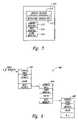
- FIG. 1is a block diagram of a computer system according to one example of the invention in which a memory hub is included in each of a plurality of memory modules.
- FIG. 2is a block diagram of a memory hub used in the computer system of FIG. 1 .
- FIG. 3is a block diagram of a portion of a DMA engine according to an embodiment of the present invention of the memory hub of FIG. 2 .
- FIG. 4is a block diagram of the tag structure according to an embodiment of the present invention used by the DMA engine of FIG. 3 .
- FIG. 5is a flow diagram for operation of a DMA engine of FIG. 3 according to an embodiment of the present invention.
- Embodiments of the present inventionare directed to a system memory having a memory hub architecture including direct memory access (DMA) capability to transfer data within the system memory without the intervention of a system processor.
- DMAdirect memory access
- FIG. 1A computer system 100 according to one example of the invention is shown in FIG. 1 .
- the computer system 100includes a processor 104 for performing various computing functions, such as executing specific software to perform specific calculations or tasks.
- the processor 104includes a processor bus 106 that normally includes an address bus, a control bus, and a data bus.
- the processor bus 106is typically coupled to cache memory 108 , which, as previously mentioned, is usually static random access memory (“SRAM”).
- SRAMstatic random access memory
- the processor bus 106is coupled to a system controller 110 , which is also sometimes referred to as a “North Bridge” or “memory controller.”
- the system controller 110serves as a communications path to the processor 104 for a variety of other components. More specifically, the system controller 110 includes a graphics port that is typically coupled to a graphics controller 112 , which is, in turn, coupled to a video terminal 114 . The system controller 110 is also coupled to one or more input devices 118 , such as a keyboard or a mouse, to allow an operator to interface with the computer system 100 . Typically, the computer system 100 also includes one or more output devices 120 , such as a printer, coupled to the processor 104 through the system controller 110 . One or more data storage devices 124 are also typically coupled to the processor 104 through the system controller 110 to allow the processor 104 to store data or retrieve data from internal or external storage media (not shown). Examples of typical storage devices 124 include hard and floppy disks, tape cassettes, and compact disk read-only memories (CD-ROMs).
- CD-ROMscompact disk read-only memories
- the system controller 110includes a memory hub controller 128 that is coupled to several memory modules 130 a , 130 b , . . . 130 n , which serve as system memory for the computer system 100 .
- the memory modules 130are preferably coupled to the memory hub controller 128 through a high-speed link 134 , which may be an optical or electrical communication path or some other type of communications path.
- the high-speed link 134is implemented as an optical communication path, the optical communication path may be in the form of one or more optical fibers, for example.
- the memory hub controller 128 and the memory moduleswill include an optical input/output port or separate input and output ports coupled to the optical communication path.
- the memory modules 130are shown coupled to the memory hub controller 128 in a point-to-point arrangement in which the high-speed link 134 is formed from coupling together the memory hubs 140 of the memory modules 130 . That is, the high speed link 134 is a bi-directional bus that couples the memory hubs 140 in series. Thus, information on the high speed link 134 must travel through the memory hubs 140 of “upstream” memory modules 130 to reach a “downstream” destination. For example, with specific reference to FIG. 1 , information transmitted from the memory hub controller 128 to the memory hub 140 of the memory module 130 c will pass through the memory hubs 140 of the memory modules 130 a and 130 b .
- topologiessuch as a coupling arrangement in which each of the memory modules 130 are coupled to the memory hub controller 128 over a high-speed link.
- a switching topologymay also be used in which the memory hub controller 128 is selectively coupled to each of the memory modules 130 through a switch (not shown).
- Other topologies that may be usedwill be apparent to one skilled in the art.
- the memory hubis coupled to four sets of memory devices 148 through a respective bus system 150 .
- Each of the setsincludes four memory devices 148 for a total of 20 memory devices 148 for each memory module 130 .
- the bus systems 150normally include a control bus, an address bus, and a data bus, as known in the art. However, it will be appreciated by those ordinarily skilled in the art that other bus systems, such as a bus system using a shared command/address bus, may also be used without departing from the scope of the present invention. It will be further appreciated that the arrangement of the memory devices 148 , and the number of memory devices 148 can be modified without departing from the scope of the present invention. In the example illustrated in FIG. 1 , the memory devices 148 are synchronous dynamic random access memory (“SDRAM”) devices. However, memory devices other than SDRAM devices may, of course, also be used.
- SDRAMsynchronous dynamic random access memory
- FIG. 2An embodiment of a memory hub 200 according to an embodiment of the present invention is shown in FIG. 2 that can be substituted for the memory hub 140 of FIG. 1 .
- the memory hub 200is shown in FIG. 2 as being coupled to four memory devices 240 a–d , which, in the present example are conventional SDRAM devices.
- the memory hub 200is coupled to four different banks of memory devices, rather than merely four different memory devices 240 a–d , each bank typically having a plurality of memory devices.
- the present descriptionwill be with reference to the memory hub 200 coupled to the four memory devices 240 a–d . It will be appreciated that the necessary modifications to the memory hub 200 to accommodate multiple banks of memory is within the knowledge of those ordinarily skilled in the art.
- link interfaces 210 a–d and 212 a–dfor coupling the memory module on which the memory hub 200 is located to a first high speed data link 220 and a second high speed data link 222 , respectively.
- the high speed data links 220 , 222can be implemented using an optical or electrical communication path or some other type of communication path.
- the link interfaces 210 a–d , 212 a–dare conventional, and include circuitry used for transferring data, command, and address information to and from the high speed data links 220 , 222 , as well known, for example, transmitter and receiver logic known in the art.
- link interfaces 210 a–d , 212 a–dto be used with the specific type of communication path, and that such modifications to the link interfaces 210 a–d , 212 a–d can be made without departing from the scope of the present invention.
- the link interfaces 210 a–d , 212 a–dwill include an optical input/output port and will convert optical signals coupled through the optical communications path into electrical signals.
- the link interfaces 210 a–d , 212 a–dare coupled to the a switch 260 through a plurality of bus and signal lines, represented by busses 214 .
- the busses 214are conventional, and include a write data bus and a read data bus, although a single bi-directional data bus may alternatively be provided to couple data in both directions through the link interfaces 210 a–d , 212 a–d . It will be appreciated by those ordinarily skilled in the art that the busses 214 are provided by way of example, and that the busses 214 may include fewer or greater signal lines, such as further including a request line and a snoop line, which can be used for maintaining cache coherency.
- the link interfaces 210 a–d , 212 a–dinclude circuitry that allow the memory hub 140 to be connected in the system memory in a variety of configurations.
- the multi-drop arrangementcan be implemented by coupling each memory module to the memory hub controller 128 through either the link interfaces 210 a–d or 212 a–d .
- a point-to-point, or daisy chain configurationas shown in FIG. 1 , can be implemented by coupling the memory modules in series.
- the link interfaces 210 a–dcan be used to couple a first memory module and the link interfaces 212 a–d can be used to couple a second memory module.
- the memory module coupled to a processor, or system controller,will be coupled thereto through one set of the link interfaces and further coupled to another memory module through the other set of link interfaces.
- the memory hub 200 of a memory moduleis coupled to the processor in a point-to-point arrangement in which there are no other devices coupled to the connection between the processor 104 and the memory hub 200 .
- This type of interconnectionprovides better signal coupling between the processor 104 and the memory hub 200 for several reasons, including relatively low capacitance, relatively few line discontinuities to reflect signals and relatively short signal paths.
- the switch 260is further coupled to four memory interfaces 270 a–d which are, in turn, coupled to the system memory devices 240 a–d , respectively.
- the switch 260is coupled to each memory interface through a plurality of bus and signal lines, represented by busses 274 .
- the busses 274include a write data bus, a read data bus, and a request line. However, it will be understood that a single bi-directional data bus may alternatively be used instead of a separate write data bus and read data bus.
- the busses 274can include a greater or lesser number of signal lines than those previously described.
- each memory interface 270 a–dis specially adapted to the system memory devices 240 a–d to which it is coupled. More specifically, each memory interface 270 a–d is specially adapted to provide and receive the specific signals received and generated, respectively, by the system memory device 240 a–d to which it is coupled. Also, the memory interfaces 270 a–d are capable of operating with system memory devices 240 a–d operating at different clock frequencies. As a result, the memory interfaces 270 a–d isolate the processor 104 from changes that may occur at the interface between the memory hub 230 and memory devices 240 a–d coupled to the memory hub 200 , and it provides a more controlled environment to which the memory devices 240 a–d may interface.
- the switch 260 coupling the link interfaces 210 a–d , 212 a–d and the memory interfaces 270 a–dcan be any of a variety of conventional or hereinafter developed switches.
- the switch 260may be a cross-bar switch that can simultaneously couple link interfaces 210 a–d , 212 a–d and the memory interfaces 270 a–d to each other in a variety of arrangements.
- the switch 260can also be a set of multiplexers that do not provide the same level of connectivity as a cross-bar switch but nevertheless can couple the some or all of the link interfaces 210 a–d , 212 a–d to each of the memory interfaces 270 a–d .
- the switch 260may also includes arbitration logic (not shown) to determine which memory accesses should receive priority over other memory accesses. Bus arbitration performing this function is well known to one skilled in the art.
- each of the memory interfaces 270 a–dincludes a respective memory controller 280 , a respective write buffer 282 , and a respective cache memory unit 284 .
- the memory controller 280performs the same functions as a conventional memory controller by providing control, address and data signals to the system memory device 240 a–d to which it is coupled and receiving data signals from the system memory device 240 a–d to which it is coupled.
- the write buffer 282 and the cache memory unit 284include the normal components of a buffer and cache memory, including a tag memory, a data memory, a comparator, and the like, as is well known in the art.
- the memory devices used in the write buffer 282 and the cache memory unit 284may be either DRAM devices, static random access memory (“SRAM”) devices, other types of memory devices, or a combination of all three. Furthermore, any or all of these memory devices as well as the other components used in the cache memory unit 284 may be either embedded or stand-alone devices.
- the write buffer 282 in each memory interface 270 a–dis used to store write requests while a read request is being serviced.
- the processor 104can issue a write request to a system memory device 240 a–d even if the memory device to which the write request is directed is busy servicing a prior write or read request.
- memory requestscan be serviced out of order since an earlier write request can be stored in the write buffer 282 while a subsequent read request is being serviced.
- the ability to buffer write requests to allow a read request to be servicedcan greatly reduce memory read latency since read requests can be given first priority regardless of their chronological order.
- a series of write requests interspersed with read requestscan be stored in the write buffer 282 to allow the read requests to be serviced in a pipelined manner followed by servicing the stored write requests in a pipelined manner.
- lengthy settling times between coupling write request to the memory devices 270 a–d and subsequently coupling read request to the memory devices 270 a–d for alternating write and read requestscan be avoided.
- each memory interface 270 a–dallows the processor 104 to receive data responsive to a read command directed to a respective system memory device 240 a–d without waiting for the memory device 240 a–d to provide such data in the event that the data was recently read from or written to that memory device 240 a–d .
- the cache memory unit 284thus reduces the read latency of the system memory devices 240 a–d to maximize the memory bandwidth of the computer system.
- the processor 104can store write data in the cache memory unit 284 and then perform other functions while the memory controller 280 in the same memory interface 270 a–d transfers the write data from the cache memory unit 284 to the system memory device 240 a–d to which it is coupled.
- a DMA engine 286coupled to the switch 260 through a bus 288 which enables the memory hub 200 to move blocks of data from one location in the system memory to another location in the system memory without intervention from the processor 104 .
- the bus 288includes a plurality of conventional bus lines and signal lines, such as address, control, data busses, and the like, for handling data transfers in the system memory.
- the DMA engine 286is able to read a link list in the system memory to execute the DMA memory operations without processor intervention, thus, freeing the processor 104 and the bandwidth limited system bus from executing the memory operations.
- the DMA engine 286is preferably an embedded circuit in the memory hub 200 .
- DMA engine 286can include circuitry to accommodate DMA operations on multiple channels. Such multiple channel DMA engines are well known in the art and can be implemented using conventional technologies.
- the processor 104writes a list of instructions in the system memory for the DMA engine 286 to execute.
- the instructionsinclude information used by the DMA engine 286 to perform the DMA operation, such as starting address of the block to move, ending address or count, destination address, the address of the next command block, and the like.
- the DMA engine 286will execute a series of continuous commands and then jump to the next command list if directed to do so.
- the DMA engine 286is programmed through a data structure that exists in one or more memory spaces.
- the data structureconsists of some number of command blocks that provide information necessary to perform data transfer operations in the system memory. Each of the command blocks can be linked through a series of address pointers to form a linked list.
- the address of the first command block in the linked listis programmed through the I/O space.
- the DMA engine 286is instructed to fetch and execute the first command block through the I/O space command register. After performing the requested data operation, an address pointer in the first command block is used to point the DMA engine 286 to the next command block. An address pointer in each successive command block is used to fetch and execute the next command block, forming a linked list.
- Each command block in the linked listis executed until a NULL pointer is encountered.
- An example of a NULL pointeris defined as an address consisting of all 1's. Upon detecting the NULL pointer, command block execution will halt, and a status bit will be set, indicating the command stream has terminated.
- Completion statuscan be contained in an I/O register in the memory hub 200 . Additionally, a start flag can also be used to indicate that the DMA engine 286 has already begun executing the DMA operation. Other status bits can indicate if the command stream has terminated normally with no errors, or abnormally due to errors. The status information may optionally generate an interrupt to the host.
- the DMA engine 286can also be used for running diagnostics in the system.
- Known good data patternscan be loaded in memory of the memory hub 200 , or known good system memory, and be used to test the system memory.
- a more detailed description of this type of applicationis provided in commonly assigned, co-pending U.S. patent application Ser. No. 10/644.522, entitled SYSTEM AND METHOD FOR ON-BOARD DIAGNOSTICS OF MEMORY MODULES, filed on , Aug. 19, 2003. which is incorporated herein by reference.
- FIG. 3is a block diagram illustrating portions of a DMA engine 300 and FIG. 4 is a block diagram illustrating a linked command list table 400 according to embodiments of the present invention.
- the DMA engine 300can be substituted for the DMA engine 286 of the memory hub 200 ( FIG. 2 ). It will be appreciated that FIG. 3 is merely a representation of the DMA engine 300 , and those ordinarily skilled in the art are provided sufficient description herein in order to practice the present invention. However, it will be further appreciated that alternative DMA engines can also be used without departing from the scope of the present invention.
- the DMA engine 300includes five registers: an address register 310 , a destination address register 311 , a control register 312 , a next register 314 , and a count register 316 , to control DMA operations.
- the starting address for the blockis loaded into the address register 310 .
- a destination address of the location to which data is to be movedis loaded into the destination address register 311 , and the length of the block is loaded into the count register 316 .
- the control register 312contains information relevant to the transfer, such as a bit indicating whether the address register 310 is to be incremented or decremented after each data item is transferred. In the present example, every time a data item is transferred by the DMA engine 300 , the count register 316 is decremented and the address register 310 is incremented. Additionally, the destination address register 311 is incremented (or decremented, depending on the control settings).
- the block transferhas been completed.
- the value in the next register 314is checked. If it points to a valid location in the system memory, the values contained in that object are loaded into the registers 310 , 312 , 314 , and 316 .
- a next block data transferthen begins automatically. However, if a NULL value, as previously described, is present in the next register 314 , the DMA operation is complete.
- the linked command list table 400 shown in FIG. 4contains a plurality of link entries 402 , 404 , and 406 , each of which contains the information necessary to reload registers 310 , 312 , 314 , and 316 .
- the link entries 402 , 404 , and 406are stored in the system memory, as previously discussed, and are linked together by pointers corresponding to the next register 314 .
- three link entries 402 , 404 , and 406are shown. These link entries, plus an initial transfer defined by writing values directly into the registers 310 , 312 , 314 , and 316 of the DMA engine 300 , define a single DMA transfer having four separate parts.
- the value NEXTpoints to the first link entry 402 .
- the first link entry 402points to the next link entry 404 in the linked command, which in turn points to the final link entry 406 .
- the final link entry 406contains the NULL value as a pointer, indicating that it is the last link entry of a DMA command list.
- the NULL valueis a reserved pointer value which does not point to a valid memory location, and is interpreted by the DMA engine 300 as a pointer to nothing. It will be appreciated that the link entries 402 , 404 , 406 are provided by way of example, and modifications thereto, such as including greater or fewer fields of information than that shown in FIG. 4 , can be made without departing from the scope of the present invention.
- FIG. 5is a flow diagram 500 illustrating the control flow used by the DMA engine 300 ( FIG. 3 ) to make a series of consecutive block transfers.
- the DMA registers 310 , 312 , 314 , and 316are loaded with the appropriate values for the first data transfer.
- all of the information necessary for the link entries for this transfermust be loaded into the linked command list table 400 ( FIG. 4 ).
- Loading of the registersis at the command of the processor 104 ( FIG. 1 ) and loading of the linked command list 400 in the system memory is accomplished by the processor 104 as well.
- one data itemis transferred, and at a step 506 , the value in the count register 316 is decremented to indicate that one data item has been transferred.
- the step 506includes simultaneously incrementing or decrementing the value of the address register 310 , depending upon the desired direction as set in the control register 312 .
- the count valueis checked to determine whether the count is complete. In one embodiment of the present invention, determination of whether the count is complete is accomplished by checking a carry out bit (not shown) from the count register 316 . In the event the count value indicates that the data transfer is not complete, control returns to the step 504 .
- the DMA engine 300implements a “scatter-gather” capability for use in the system memory.
- the processor 104allocates the memory and sets up the linked command list table 400 through the DMA engine 300 .
- a DMA transferis then initiated, and the DMA engine 300 handles the entire transfer until it is completed.
- a similar techniquecan be used for gathering scattered blocks of data within the system memory in order to write them to consecutive blocks of memory.
- the processor 104determines which blocks are to be written moved within the system memory, and their order, and sets up the linked command list table 400 through the DMA engine 300 .
- a DMA transferis then initiated, and is handled completely by the DMA engine 300 until it is completed. Since the linked command list table 400 is stored in the system memory, it is possible to keep several linked lists, for example, for each channel supported by the DMA engine 300 . Moreover, since the linked command list table 400 is stored in the system memory, the only limit on the number of separate transfers which may be linked into one larger transfer for a channel is the number of remaining free memory locations within the system memory.
Landscapes
- Engineering & Computer Science (AREA)
- Theoretical Computer Science (AREA)
- General Engineering & Computer Science (AREA)
- Physics & Mathematics (AREA)
- General Physics & Mathematics (AREA)
- Computer Hardware Design (AREA)
- Bus Control (AREA)
- Information Retrieval, Db Structures And Fs Structures Therefor (AREA)
Abstract
Description
This application is a divisional of pending U.S. patent application Ser. No. 10/625,132, filed Jul. 22, 2003.
This invention relates to computer systems, and, more particularly, to a computer system including a system memory having a memory hub architecture.
Computer systems use memory devices, such as dynamic random access memory (“DRAM”) devices, to store data that are accessed by a processor. These memory devices are normally used as system memory in a computer system. In a typical computer system, the processor communicates with the system memory through a processor bus and a memory controller. The processor issues a memory request, which includes a memory command, such as a read command, and an address designating the location from which data or instructions are to be read. The memory controller uses the command and address to generate appropriate command signals as well as row and column addresses, which are applied to the system memory. In response to the commands and addresses, data are transferred between the system memory and the processor. The memory controller is often part of a system controller, which also includes bus bridge circuitry for coupling the processor bus to an expansion bus, such as a PCI bus.
Although the operating speed of memory devices has continuously increased, this increase in operating speed has not kept pace with increases in the operating speed of processors. Even slower has been the increase in operating speed of memory controllers coupling processors to memory devices. The relatively slow speed of memory controllers and memory devices limits the data bandwidth between the processor and the memory devices.
In addition to the limited bandwidth between processors and memory devices, the performance of computer systems is also limited by latency problems that increase the time required to read data from system memory devices. More specifically, when a memory device read command is coupled to a system memory device, such as a synchronous DRAM (“SDRAM”) device, the read data are output from the SDRAM device only after a delay of several clock periods. Therefore, although SDRAM devices can synchronously output burst data at a high data rate, the delay in initially providing the data can significantly slow the operating speed of a computer system using such SDRAM devices.
One approach to alleviating the memory latency problem is to use multiple memory devices coupled to the processor through a memory hub. In a memory hub architecture, a system controller or memory controller is coupled over a high speed data link to several memory modules. Typically, the memory modules are coupled in a point-to-point or daisy chain architecture such that the memory modules are connected one to another in series. Thus, the memory controller is coupled to a first memory module over a first high speed data link, with the first memory module connected to a second memory module through a second high speed data link, and the second memory module coupled to a third memory module through a third high speed data link, and so on in a daisy chain fashion.
Each memory module includes a memory hub that is coupled to the corresponding high speed data links and a number of memory devices on the module, with the memory hubs efficiently routing memory requests and responses between the controller and the memory devices over the high speed data links. Computer systems employing this architecture can have a higher bandwidth because a processor can access one memory device while another memory device is responding to a prior memory access. For example, the processor can output write data to one of the memory devices in the system while another memory device in the system is preparing to provide read data to the processor. Moreover, this architecture also provides for easy expansion of the system memory without concern for degradation in signal quality as more memory modules are added, such as occurs in conventional multi-drop bus architectures.
Although computer systems using memory hubs may provide superior performance, they nevertheless may often fail to operate at optimum speeds for a variety of reasons. For example, even though memory hubs can provide computer systems with a greater memory bandwidth, they still suffer from latency problems of the type described above. More specifically, although the processor may communicate with one memory device while another memory device is preparing to transfer data, it is sometimes necessary to receive data from one memory device before the data from another memory device can be used. In the event data must be received from one memory device before data received from another memory device can be used, the intervention of the processor continues to slow the operating speed of such computer systems. Another one of the reasons such computer systems fail to operate at optimum speed is that conventional memory hubs are essentially single channel systems since all control, address and data signals must pass through common memory hub circuitry. As a result, when the memory hub circuitry is busy communicating with one memory device, it is not free to communicate with another memory device.
One technique that has been used in computer systems to overcome the issues with processor intervention in moving data to and from memory as well as the single channel bottleneck is the use of direct memory access (DMA) operations. DMA operations are implemented through the use of DMA controllers included in the computer system which enable data to be moved into and out of memory without the intervention of the system processor. Such DMA operations and DMA controllers are well known in the art, and are often implemented in conventional computer systems. The DMA controller removes the need for the processor to be involved and manages the required data transfers into and out of the system memory. For example, when a DMA supported entity transfers data to the system memory, the DMA controller obtains control of the bus and coordinates the transfer of the data from the DMA supported entity to the system memory, without involvement by the processor. In this manner, latency issues resulting from processor intervention can be avoided during data transfers across the system bus. However, in many instances, even after data has been transferred to the system memory through a DMA operation, the processor nevertheless must move blocks of the data from one location to another within the system memory. For example, the operating system will direct a DMA operation to transfer data from a mass storage device into the system memory, only to have the processor then move the data again to another location in memory so the data can be used. As a result, the value of having DMA operations is diminished to some degree because the processor ultimately becomes involved by moving data around in memory despite the use of a DMA operation in the data transfer to and from the system memory.
Therefore, there is a need for a computer architecture that provides the advantages of a memory hub architecture and also minimizes the latency problems common in such systems.
The present invention is directed to a memory hub for a memory module having a DMA engine for performing DMA operations in system memory. The memory hub includes a link interface for receiving memory requests for access to at least one of the memory devices of the system memory, and further including a memory device interface for coupling to the memory devices, the memory device interface coupling memory requests to the memory devices for access to at least one of the memory devices. A switch for selectively coupling the link interface and the memory device interface is further included in the memory hub. Additionally, a direct memory access (DMA) engine is coupled through the switch to the memory device interface to generate memory requests for access to at least one of the memory devices to perform DMA operations.
In an aspect of the present invention, a method is provided for executing memory operations in a computer system having a processor, a system controller coupled to the processor, and a system memory having at least one memory module coupled to the system controller through a memory bus. The method includes writing DMA information to a location in the system memory representing instructions for executing memory operations in the system memory without processor intervention, obtaining control of the memory bus from the processor and system controller, accessing the location in the system memory to which the DMA information is written, and executing the memory operations represented by the instructions.
Embodiments of the present invention are directed to a system memory having a memory hub architecture including direct memory access (DMA) capability to transfer data within the system memory without the intervention of a system processor. Certain details are set forth below to provide a sufficient understanding of the invention. However, it will be clear to one skilled in the art that the invention may be practiced without these particular details. In other instances, well-known circuits, control signals, and timing protocols have not been shown in detail in order to avoid unnecessarily obscuring the invention.
Acomputer system 100 according to one example of the invention is shown inFIG. 1 . Thecomputer system 100 includes aprocessor 104 for performing various computing functions, such as executing specific software to perform specific calculations or tasks. Theprocessor 104 includes aprocessor bus 106 that normally includes an address bus, a control bus, and a data bus. Theprocessor bus 106 is typically coupled to cachememory 108, which, as previously mentioned, is usually static random access memory (“SRAM”). Finally, theprocessor bus 106 is coupled to asystem controller 110, which is also sometimes referred to as a “North Bridge” or “memory controller.”
Thesystem controller 110 serves as a communications path to theprocessor 104 for a variety of other components. More specifically, thesystem controller 110 includes a graphics port that is typically coupled to agraphics controller 112, which is, in turn, coupled to avideo terminal 114. Thesystem controller 110 is also coupled to one ormore input devices 118, such as a keyboard or a mouse, to allow an operator to interface with thecomputer system 100. Typically, thecomputer system 100 also includes one ormore output devices 120, such as a printer, coupled to theprocessor 104 through thesystem controller 110. One or moredata storage devices 124 are also typically coupled to theprocessor 104 through thesystem controller 110 to allow theprocessor 104 to store data or retrieve data from internal or external storage media (not shown). Examples oftypical storage devices 124 include hard and floppy disks, tape cassettes, and compact disk read-only memories (CD-ROMs).
Thesystem controller 110 includes amemory hub controller 128 that is coupled toseveral memory modules computer system 100. The memory modules130 are preferably coupled to thememory hub controller 128 through a high-speed link 134, which may be an optical or electrical communication path or some other type of communications path. In the event the high-speed link 134 is implemented as an optical communication path, the optical communication path may be in the form of one or more optical fibers, for example. In such case, thememory hub controller 128 and the memory modules will include an optical input/output port or separate input and output ports coupled to the optical communication path.
The memory modules130 are shown coupled to thememory hub controller 128 in a point-to-point arrangement in which the high-speed link 134 is formed from coupling together thememory hubs 140 of the memory modules130. That is, thehigh speed link 134 is a bi-directional bus that couples thememory hubs 140 in series. Thus, information on thehigh speed link 134 must travel through thememory hubs 140 of “upstream” memory modules130 to reach a “downstream” destination. For example, with specific reference toFIG. 1 , information transmitted from thememory hub controller 128 to thememory hub 140 of thememory module 130cwill pass through thememory hubs 140 of thememory modules memory hub controller 128 over a high-speed link. A switching topology may also be used in which thememory hub controller 128 is selectively coupled to each of the memory modules130 through a switch (not shown). Other topologies that may be used will be apparent to one skilled in the art.
As also shown inFIG. 1 , the memory hub is coupled to four sets ofmemory devices 148 through arespective bus system 150. Each of the sets includes fourmemory devices 148 for a total of 20memory devices 148 for each memory module130. Thebus systems 150 normally include a control bus, an address bus, and a data bus, as known in the art. However, it will be appreciated by those ordinarily skilled in the art that other bus systems, such as a bus system using a shared command/address bus, may also be used without departing from the scope of the present invention. It will be further appreciated that the arrangement of thememory devices 148, and the number ofmemory devices 148 can be modified without departing from the scope of the present invention. In the example illustrated inFIG. 1 , thememory devices 148 are synchronous dynamic random access memory (“SDRAM”) devices. However, memory devices other than SDRAM devices may, of course, also be used.
An embodiment of amemory hub 200 according to an embodiment of the present invention is shown inFIG. 2 that can be substituted for thememory hub 140 ofFIG. 1 . Thememory hub 200 is shown inFIG. 2 as being coupled to fourmemory devices 240a–d, which, in the present example are conventional SDRAM devices. In an alternative embodiment, thememory hub 200 is coupled to four different banks of memory devices, rather than merely fourdifferent memory devices 240a–d, each bank typically having a plurality of memory devices. However, for the purpose of providing an example, the present description will be with reference to thememory hub 200 coupled to the fourmemory devices 240a–d. It will be appreciated that the necessary modifications to thememory hub 200 to accommodate multiple banks of memory is within the knowledge of those ordinarily skilled in the art.
Further included in thememory hub 200 arelink interfaces 210a–dand212a–dfor coupling the memory module on which thememory hub 200 is located to a first highspeed data link 220 and a second highspeed data link 222, respectively. As previously discussed with respect toFIG. 1 , the highspeed data links speed data links speed data link
The link interfaces210a–d,212a–dare coupled to the aswitch 260 through a plurality of bus and signal lines, represented bybusses 214. Thebusses 214 are conventional, and include a write data bus and a read data bus, although a single bi-directional data bus may alternatively be provided to couple data in both directions through the link interfaces210a–d,212a–d. It will be appreciated by those ordinarily skilled in the art that thebusses 214 are provided by way of example, and that thebusses 214 may include fewer or greater signal lines, such as further including a request line and a snoop line, which can be used for maintaining cache coherency.
The link interfaces210a–d,212a–dinclude circuitry that allow thememory hub 140 to be connected in the system memory in a variety of configurations. For example, the multi-drop arrangement, can be implemented by coupling each memory module to thememory hub controller 128 through either the link interfaces210a–dor212a–d. Alternatively, a point-to-point, or daisy chain configuration, as shown inFIG. 1 , can be implemented by coupling the memory modules in series. For example, the link interfaces210a–dcan be used to couple a first memory module and the link interfaces212a–dcan be used to couple a second memory module. The memory module coupled to a processor, or system controller, will be coupled thereto through one set of the link interfaces and further coupled to another memory module through the other set of link interfaces. In one embodiment of the present invention, thememory hub 200 of a memory module is coupled to the processor in a point-to-point arrangement in which there are no other devices coupled to the connection between theprocessor 104 and thememory hub 200. This type of interconnection provides better signal coupling between theprocessor 104 and thememory hub 200 for several reasons, including relatively low capacitance, relatively few line discontinuities to reflect signals and relatively short signal paths.
Theswitch 260 is further coupled to fourmemory interfaces 270a–dwhich are, in turn, coupled to thesystem memory devices 240a–d, respectively. By providing a separate andindependent memory interface 270a–dfor eachsystem memory device 240a–d, respectively, thememory hub 200 avoids bus or memory bank conflicts that typically occur with single channel memory architectures. Theswitch 260 is coupled to each memory interface through a plurality of bus and signal lines, represented by busses274. The busses274 include a write data bus, a read data bus, and a request line. However, it will be understood that a single bi-directional data bus may alternatively be used instead of a separate write data bus and read data bus. Moreover, the busses274 can include a greater or lesser number of signal lines than those previously described.
In an embodiment of the present invention, eachmemory interface 270a–dis specially adapted to thesystem memory devices 240a–dto which it is coupled. More specifically, eachmemory interface 270a–dis specially adapted to provide and receive the specific signals received and generated, respectively, by thesystem memory device 240a–dto which it is coupled. Also, the memory interfaces270a–dare capable of operating withsystem memory devices 240a–doperating at different clock frequencies. As a result, the memory interfaces270a–disolate theprocessor 104 from changes that may occur at the interface between the memory hub230 andmemory devices 240a–dcoupled to thememory hub 200, and it provides a more controlled environment to which thememory devices 240a–dmay interface.
Theswitch 260 coupling the link interfaces210a–d,212a–dand the memory interfaces270a–dcan be any of a variety of conventional or hereinafter developed switches. For example, theswitch 260 may be a cross-bar switch that can simultaneously couple link interfaces210a–d,212a–dand the memory interfaces270a–dto each other in a variety of arrangements. Theswitch 260 can also be a set of multiplexers that do not provide the same level of connectivity as a cross-bar switch but nevertheless can couple the some or all of the link interfaces210a–d,212a–dto each of the memory interfaces270a–d. Theswitch 260 may also includes arbitration logic (not shown) to determine which memory accesses should receive priority over other memory accesses. Bus arbitration performing this function is well known to one skilled in the art.
With further reference toFIG. 2 , each of the memory interfaces270a–dincludes a respective memory controller280, a respective write buffer282, and a respective cache memory unit284. The memory controller280 performs the same functions as a conventional memory controller by providing control, address and data signals to thesystem memory device 240a–dto which it is coupled and receiving data signals from thesystem memory device 240a–dto which it is coupled. The write buffer282 and the cache memory unit284 include the normal components of a buffer and cache memory, including a tag memory, a data memory, a comparator, and the like, as is well known in the art. The memory devices used in the write buffer282 and the cache memory unit284 may be either DRAM devices, static random access memory (“SRAM”) devices, other types of memory devices, or a combination of all three. Furthermore, any or all of these memory devices as well as the other components used in the cache memory unit284 may be either embedded or stand-alone devices.
The write buffer282 in eachmemory interface 270a–dis used to store write requests while a read request is being serviced. In a such a system, theprocessor 104 can issue a write request to asystem memory device 240a–deven if the memory device to which the write request is directed is busy servicing a prior write or read request. Using this approach, memory requests can be serviced out of order since an earlier write request can be stored in the write buffer282 while a subsequent read request is being serviced. The ability to buffer write requests to allow a read request to be serviced can greatly reduce memory read latency since read requests can be given first priority regardless of their chronological order. For example, a series of write requests interspersed with read requests can be stored in the write buffer282 to allow the read requests to be serviced in a pipelined manner followed by servicing the stored write requests in a pipelined manner. As a result, lengthy settling times between coupling write request to thememory devices 270a–dand subsequently coupling read request to thememory devices 270a–dfor alternating write and read requests can be avoided.
The use of the cache memory unit284 in eachmemory interface 270a–dallows theprocessor 104 to receive data responsive to a read command directed to a respectivesystem memory device 240a–dwithout waiting for thememory device 240a–dto provide such data in the event that the data was recently read from or written to thatmemory device 240a–d. The cache memory unit284 thus reduces the read latency of thesystem memory devices 240a–dto maximize the memory bandwidth of the computer system. Similarly, theprocessor 104 can store write data in the cache memory unit284 and then perform other functions while the memory controller280 in thesame memory interface 270a–dtransfers the write data from the cache memory unit284 to thesystem memory device 240a–dto which it is coupled.
Further included in thememory hub 200 is aDMA engine 286 coupled to theswitch 260 through abus 288 which enables thememory hub 200 to move blocks of data from one location in the system memory to another location in the system memory without intervention from theprocessor 104. Thebus 288 includes a plurality of conventional bus lines and signal lines, such as address, control, data busses, and the like, for handling data transfers in the system memory. As will be described in more detail below, theDMA engine 286 is able to read a link list in the system memory to execute the DMA memory operations without processor intervention, thus, freeing theprocessor 104 and the bandwidth limited system bus from executing the memory operations. TheDMA engine 286 is preferably an embedded circuit in thememory hub 200. However, including a separate DMA device coupled to thememory hub 200 is also within the scope of the present invention. Additionally, theDMA engine 286 can include circuitry to accommodate DMA operations on multiple channels. Such multiple channel DMA engines are well known in the art and can be implemented using conventional technologies.
In an embodiment of the present invention, theprocessor 104 writes a list of instructions in the system memory for theDMA engine 286 to execute. The instructions include information used by theDMA engine 286 to perform the DMA operation, such as starting address of the block to move, ending address or count, destination address, the address of the next command block, and the like. TheDMA engine 286 will execute a series of continuous commands and then jump to the next command list if directed to do so. TheDMA engine 286 is programmed through a data structure that exists in one or more memory spaces. The data structure consists of some number of command blocks that provide information necessary to perform data transfer operations in the system memory. Each of the command blocks can be linked through a series of address pointers to form a linked list. The address of the first command block in the linked list is programmed through the I/O space. TheDMA engine 286 is instructed to fetch and execute the first command block through the I/O space command register. After performing the requested data operation, an address pointer in the first command block is used to point theDMA engine 286 to the next command block. An address pointer in each successive command block is used to fetch and execute the next command block, forming a linked list. Each command block in the linked list is executed until a NULL pointer is encountered. An example of a NULL pointer is defined as an address consisting of all 1's. Upon detecting the NULL pointer, command block execution will halt, and a status bit will be set, indicating the command stream has terminated. Completion status can be contained in an I/O register in thememory hub 200. Additionally, a start flag can also be used to indicate that theDMA engine 286 has already begun executing the DMA operation. Other status bits can indicate if the command stream has terminated normally with no errors, or abnormally due to errors. The status information may optionally generate an interrupt to the host.
In alternative embodiments of the present invention, theDMA engine 286 can also be used for running diagnostics in the system. Known good data patterns can be loaded in memory of thememory hub 200, or known good system memory, and be used to test the system memory. A more detailed description of this type of application is provided in commonly assigned, co-pending U.S. patent application Ser. No. 10/644.522, entitled SYSTEM AND METHOD FOR ON-BOARD DIAGNOSTICS OF MEMORY MODULES, filed on , Aug. 19, 2003. which is incorporated herein by reference.
In operation, at the beginning of a block transfer, the starting address for the block is loaded into theaddress register 310. Additionally, a destination address of the location to which data is to be moved is loaded into thedestination address register 311, and the length of the block is loaded into thecount register 316. The control register312 contains information relevant to the transfer, such as a bit indicating whether theaddress register 310 is to be incremented or decremented after each data item is transferred. In the present example, every time a data item is transferred by theDMA engine 300, thecount register 316 is decremented and theaddress register 310 is incremented. Additionally, thedestination address register 311 is incremented (or decremented, depending on the control settings). When the value of thecount register 316 reaches zero, the block transfer has been completed. At this time, the value in thenext register 314 is checked. If it points to a valid location in the system memory, the values contained in that object are loaded into theregisters next register 314, the DMA operation is complete.
The linked command list table400 shown inFIG. 4 contains a plurality oflink entries registers link entries next register 314. InFIG. 4 , threelink entries registers DMA engine 300, define a single DMA transfer having four separate parts. The value NEXT, contained in thenext register 314, points to thefirst link entry 402. Thefirst link entry 402 points to thenext link entry 404 in the linked command, which in turn points to thefinal link entry 406. Thefinal link entry 406 contains the NULL value as a pointer, indicating that it is the last link entry of a DMA command list. The NULL value is a reserved pointer value which does not point to a valid memory location, and is interpreted by theDMA engine 300 as a pointer to nothing. It will be appreciated that thelink entries FIG. 4 , can be made without departing from the scope of the present invention.
At astep 504, one data item is transferred, and at astep 506, the value in thecount register 316 is decremented to indicate that one data item has been transferred. Thestep 506 includes simultaneously incrementing or decrementing the value of theaddress register 310, depending upon the desired direction as set in thecontrol register 312. At astep 508, the count value is checked to determine whether the count is complete. In one embodiment of the present invention, determination of whether the count is complete is accomplished by checking a carry out bit (not shown) from thecount register 316. In the event the count value indicates that the data transfer is not complete, control returns to thestep 504. However, if the count value in thecount register 316 is equal to zero, control passes to astep 510, where the value in thenext register 314 is tested to see if it is equal to the NULL value, as previously described. If a NULL value is not present, at astep 512 the next tag is loaded into theregisters DMA controller 300 from the linked command list table400, and control returns to thestep 504. Once the last link entry has been used, at astep 514 an indication is made to theprocessor 104 that the transfer is complete.
It will be appreciated by those ordinarily skilled in the art that theDMA engine 300 implements a “scatter-gather” capability for use in the system memory. When a large block of data is to be read into nonconsecutive blocks of memory, theprocessor 104 allocates the memory and sets up the linked command list table400 through theDMA engine 300. A DMA transfer is then initiated, and theDMA engine 300 handles the entire transfer until it is completed. A similar technique can be used for gathering scattered blocks of data within the system memory in order to write them to consecutive blocks of memory. Theprocessor 104 determines which blocks are to be written moved within the system memory, and their order, and sets up the linked command list table400 through theDMA engine 300. A DMA transfer is then initiated, and is handled completely by theDMA engine 300 until it is completed. Since the linked command list table400 is stored in the system memory, it is possible to keep several linked lists, for example, for each channel supported by theDMA engine 300. Moreover, since the linked command list table400 is stored in the system memory, the only limit on the number of separate transfers which may be linked into one larger transfer for a channel is the number of remaining free memory locations within the system memory.
From the foregoing it will be appreciated that, although specific embodiments of the invention have been described herein for purposes of illustration, various modifications may be made without deviating from the spirit and scope of the invention. Accordingly, the invention is not limited except as by the appended claims.
Claims (8)
1. A method for executing memory operations in a computer system having a processor, a system controller coupled to the processor, and a system memory having at least one memory module coupled to the system controller through a memory bus, the method comprising:
writing direct memory access (DMA) information to a location in the system memory representing instructions for executing memory operations in the system memory without processor intervention;
obtaining control of the memory bus from the processor and system controller; and
using a DMA controller located on the memory module, accessing the location in the system memory to which the DMA information is written and handling execution of the memory operations represented by the instructions by the DMA controller on the memory module until completion of the memory operations.
2. The method ofclaim 1 , further comprising isolating the system memory during execution of the memory operations.
3. The method ofclaim 1 wherein writing DMA information comprises:
writing a starting memory address of a memory location in the system memory at which the memory operations begins;
writing a target address of a memory location in the system memory to which data is to be moved in the memory operations;
writing a count value indicative of the number of memory locations to be accessed in the memory operations; and
writing a next memory address value representative of the completion of the memory operations or representative of a memory address corresponding to a link list including a starting memory address, a count value and a next memory address value.
4. The method ofclaim 1 wherein the system memory comprises a plurality of memory modules and wherein executing the memory operations comprises accessing a memory location in a first of the plurality of memory modules to read data therefrom and accessing a memory location in a second of the plurality of memory modules to write the data.
5. A method for transferring data within a system memory included in a computer system having a processor, a system controller coupled to the processor, and a memory bus coupling the system controller to the system memory, the method comprising:
writing DMA instructions to a location in the system memory, the DMA instructions representing instructions for executing memory operations to transfer the data including memory addresses corresponding to first and second locations in the system memory;
obtaining control of the memory bus; and
without processor and system controller intervention and using a DMA controller located on a memory module of the system memory, accessing the location in the system memory at which the DMA instructions are written, reading data from the first location in the system memory and writing the data to the second location in the system memory.
6. The method ofclaim 5 wherein obtaining control of the memory bus comprises isolating the system memory from the processor and system controller while transferring data within the system memory.
7. The method ofclaim 5 wherein writing DMA instructions comprises:
writing a starting memory address of a memory location in the system memory at which the transfer of data begins;
writing a target address of a memory location in the system memory to which the data is to be transferred;
writing a count value indicative of the number of memory locations to be accessed in transferring the data; and
writing a next memory address value representative of the completion of the data transfer or representative of a memory address corresponding to a link list including a starting memory address, a count value and a next memory address value.
8. The method ofclaim 5 wherein the system memory comprises a plurality of memory modules and wherein reading data from the first location in the system memory comprises accessing a memory location in a first of the plurality of memory modules to read data therefrom and writing the data to the second location in the system memory comprises accessing a memory location in a second of the plurality of memory modules to write the data.
Priority Applications (1)
| Application Number | Priority Date | Filing Date | Title |
|---|---|---|---|
| US11/065,990US7222197B2 (en) | 2003-07-22 | 2005-02-24 | Apparatus and method for direct memory access in a hub-based memory system |
Applications Claiming Priority (2)
| Application Number | Priority Date | Filing Date | Title |
|---|---|---|---|
| US10/625,132US7389364B2 (en) | 2003-07-22 | 2003-07-22 | Apparatus and method for direct memory access in a hub-based memory system |
| US11/065,990US7222197B2 (en) | 2003-07-22 | 2005-02-24 | Apparatus and method for direct memory access in a hub-based memory system |
Related Parent Applications (1)
| Application Number | Title | Priority Date | Filing Date |
|---|---|---|---|
| US10/625,132DivisionUS7389364B2 (en) | 2003-07-22 | 2003-07-22 | Apparatus and method for direct memory access in a hub-based memory system |
Publications (2)
| Publication Number | Publication Date |
|---|---|
| US20050160201A1 US20050160201A1 (en) | 2005-07-21 |
| US7222197B2true US7222197B2 (en) | 2007-05-22 |
Family
ID=34080141
Family Applications (4)
| Application Number | Title | Priority Date | Filing Date |
|---|---|---|---|
| US10/625,132Expired - Fee RelatedUS7389364B2 (en) | 2003-07-22 | 2003-07-22 | Apparatus and method for direct memory access in a hub-based memory system |
| US11/065,990Expired - Fee RelatedUS7222197B2 (en) | 2003-07-22 | 2005-02-24 | Apparatus and method for direct memory access in a hub-based memory system |
| US12/112,812Expired - Fee RelatedUS7966430B2 (en) | 2003-07-22 | 2008-04-30 | Apparatus and method for direct memory access in a hub-based memory system |
| US13/164,156Expired - Fee RelatedUS8209445B2 (en) | 2003-07-22 | 2011-06-20 | Apparatus and method for direct memory access in a hub-based memory system |
Family Applications Before (1)
| Application Number | Title | Priority Date | Filing Date |
|---|---|---|---|
| US10/625,132Expired - Fee RelatedUS7389364B2 (en) | 2003-07-22 | 2003-07-22 | Apparatus and method for direct memory access in a hub-based memory system |
Family Applications After (2)
| Application Number | Title | Priority Date | Filing Date |
|---|---|---|---|
| US12/112,812Expired - Fee RelatedUS7966430B2 (en) | 2003-07-22 | 2008-04-30 | Apparatus and method for direct memory access in a hub-based memory system |
| US13/164,156Expired - Fee RelatedUS8209445B2 (en) | 2003-07-22 | 2011-06-20 | Apparatus and method for direct memory access in a hub-based memory system |
Country Status (10)
| Country | Link |
|---|---|
| US (4) | US7389364B2 (en) |
| EP (2) | EP2256587A1 (en) |
| JP (1) | JP4560646B2 (en) |
| KR (1) | KR100887526B1 (en) |
| CN (1) | CN100595720C (en) |
| AT (1) | ATE479138T1 (en) |
| DE (1) | DE602004028831D1 (en) |
| SG (1) | SG129443A1 (en) |
| TW (1) | TW200517848A (en) |
| WO (1) | WO2005010670A2 (en) |
Cited By (7)
| Publication number | Priority date | Publication date | Assignee | Title |
|---|---|---|---|---|
| US20050023560A1 (en)* | 2003-07-28 | 2005-02-03 | Ahn Young-Man | Memory module test system |
| US20070191993A1 (en)* | 2006-02-16 | 2007-08-16 | Intel Corporation | Thermal management using an on-die thermal sensor |
| US20090132781A1 (en)* | 2003-09-18 | 2009-05-21 | Schnepper Randy L | Memory hub with integrated non-volatile memory |
| US20140108869A1 (en)* | 2012-10-15 | 2014-04-17 | Infineon Technologies Ag | DMA Integrity Checker |
| US10191871B2 (en) | 2017-06-20 | 2019-01-29 | Infineon Technologies Ag | Safe double buffering using DMA safe linked lists |
| US11074169B2 (en) | 2013-07-03 | 2021-07-27 | Micron Technology, Inc. | Programmed memory controlled data movement and timing within a main memory device |
| US11853179B1 (en)* | 2018-12-28 | 2023-12-26 | Teledyne Lecroy, Inc. | Detection of a DMA (direct memory access) memory address violation when testing PCIE devices |
Families Citing this family (37)
| Publication number | Priority date | Publication date | Assignee | Title |
|---|---|---|---|---|
| US6953392B2 (en)* | 2001-01-05 | 2005-10-11 | Asm Nutool, Inc. | Integrated system for processing semiconductor wafers |
| US20040093439A1 (en)* | 2002-09-24 | 2004-05-13 | Rohm Co., Ltd | Data processing control apparatus and DMA controller |
| DE112004000821B4 (en)* | 2003-05-13 | 2016-12-01 | Advanced Micro Devices, Inc. | System with a host connected to multiple storage modules via a serial storage connection |
| US7428644B2 (en)* | 2003-06-20 | 2008-09-23 | Micron Technology, Inc. | System and method for selective memory module power management |
| US7389364B2 (en)* | 2003-07-22 | 2008-06-17 | Micron Technology, Inc. | Apparatus and method for direct memory access in a hub-based memory system |
| US7210059B2 (en)* | 2003-08-19 | 2007-04-24 | Micron Technology, Inc. | System and method for on-board diagnostics of memory modules |
| US7133991B2 (en)* | 2003-08-20 | 2006-11-07 | Micron Technology, Inc. | Method and system for capturing and bypassing memory transactions in a hub-based memory system |
| US7310752B2 (en) | 2003-09-12 | 2007-12-18 | Micron Technology, Inc. | System and method for on-board timing margin testing of memory modules |
| US7120743B2 (en) | 2003-10-20 | 2006-10-10 | Micron Technology, Inc. | Arbitration system and method for memory responses in a hub-based memory system |
| US7216196B2 (en)* | 2003-12-29 | 2007-05-08 | Micron Technology, Inc. | Memory hub and method for memory system performance monitoring |
| JP4441286B2 (en)* | 2004-02-10 | 2010-03-31 | 株式会社日立製作所 | Storage system |
| US7467238B2 (en) | 2004-02-10 | 2008-12-16 | Hitachi, Ltd. | Disk controller and storage system |
| JP4405277B2 (en) | 2004-02-16 | 2010-01-27 | 株式会社日立製作所 | Disk controller |
| US8177129B2 (en)* | 2004-02-17 | 2012-05-15 | Timothy D. Larin | Interactive multimedia smart affinity card with flash memory |
| US7310748B2 (en) | 2004-06-04 | 2007-12-18 | Micron Technology, Inc. | Memory hub tester interface and method for use thereof |
| US7739423B2 (en)* | 2004-11-30 | 2010-06-15 | Broadcom Corporation | Bulk transfer of information on network device |
| JP4581815B2 (en)* | 2005-04-26 | 2010-11-17 | セイコーエプソン株式会社 | Printing control apparatus and printing system |
| US20060259657A1 (en)* | 2005-05-10 | 2006-11-16 | Telairity Semiconductor, Inc. | Direct memory access (DMA) method and apparatus and DMA for video processing |
| WO2006121443A2 (en)* | 2005-05-10 | 2006-11-16 | Telairity Semiconductor, Inc. | Direct memory access (dma) method and apparatus and dma for video processing |
| US8341360B2 (en) | 2005-12-30 | 2012-12-25 | Intel Corporation | Method and apparatus for memory write performance optimization in architectures with out-of-order read/request-for-ownership response |
| WO2008014413A2 (en)* | 2006-07-27 | 2008-01-31 | Rambus Inc. | Cross-threaded memory device and system |
| US7769942B2 (en) | 2006-07-27 | 2010-08-03 | Rambus, Inc. | Cross-threaded memory system |
| JP4389921B2 (en) | 2006-10-25 | 2009-12-24 | セイコーエプソン株式会社 | Data transfer circuit and semiconductor integrated circuit having the same |
| US20080183959A1 (en)* | 2007-01-29 | 2008-07-31 | Pelley Perry H | Memory system having global buffered control for memory modules |
| US8880970B2 (en)* | 2008-12-23 | 2014-11-04 | Conversant Intellectual Property Management Inc. | Error detection method and a system including one or more memory devices |
| US8621159B2 (en) | 2009-02-11 | 2013-12-31 | Rambus Inc. | Shared access memory scheme |
| US10095433B1 (en) | 2012-10-24 | 2018-10-09 | Western Digital Technologies, Inc. | Out-of-order data transfer mechanisms for data storage systems |
| US10049061B2 (en) | 2012-11-12 | 2018-08-14 | International Business Machines Corporation | Active memory device gather, scatter, and filter |
| US9141541B2 (en) | 2013-09-20 | 2015-09-22 | Advanced Micro Devices, Inc. | Nested channel address interleaving |
| US9476938B2 (en)* | 2013-09-27 | 2016-10-25 | Novachips Canada Inc. | Method and apparatus for testing surface mounted devices |
| CN110299157B (en) | 2013-11-11 | 2023-04-28 | 拉姆伯斯公司 | Mass storage system using standard controller components |
| CN104317750B (en)* | 2014-10-23 | 2018-01-05 | 山西达鑫核科技有限公司 | A kind of storage medium structure that can independently stack connection |
| KR102428563B1 (en)* | 2015-09-30 | 2022-08-03 | 삼성전자주식회사 | Coherent interconnect for managing snoop operation and data processing apparatus including the same |
| US10783103B1 (en)* | 2017-02-24 | 2020-09-22 | Xilinx, Inc. | Split control for direct memory access transfers |
| KR20190123984A (en)* | 2018-04-25 | 2019-11-04 | 에스케이하이닉스 주식회사 | Memory system and operating method thereof |
| US10990307B2 (en)* | 2018-07-27 | 2021-04-27 | Broadcom International Pte. Ltd. | System and method for providing a configurable storage media interface |
| FR3094507A1 (en) | 2019-03-29 | 2020-10-02 | Stmicroelectronics (Grenoble 2) Sas | Direct memory access |
Citations (242)
| Publication number | Priority date | Publication date | Assignee | Title |
|---|---|---|---|---|
| US4045781A (en) | 1976-02-13 | 1977-08-30 | Digital Equipment Corporation | Memory module with selectable byte addressing for digital data processing system |
| US4240143A (en) | 1978-12-22 | 1980-12-16 | Burroughs Corporation | Hierarchical multi-processor network for memory sharing |
| US4245306A (en) | 1978-12-21 | 1981-01-13 | Burroughs Corporation | Selection of addressed processor in a multi-processor network |
| US4253146A (en) | 1978-12-21 | 1981-02-24 | Burroughs Corporation | Module for coupling computer-processors |
| US4253144A (en) | 1978-12-21 | 1981-02-24 | Burroughs Corporation | Multi-processor communication network |
| US4608702A (en) | 1984-12-21 | 1986-08-26 | Advanced Micro Devices, Inc. | Method for digital clock recovery from Manchester-encoded signals |
| US4641249A (en) | 1983-06-22 | 1987-02-03 | Kuraray Co., Ltd. | Method and device for compensating temperature-dependent characteristic changes in ion-sensitive FET transducer |
| US4707823A (en) | 1986-07-21 | 1987-11-17 | Chrysler Motors Corporation | Fiber optic multiplexed data acquisition system |
| US4724520A (en) | 1985-07-01 | 1988-02-09 | United Technologies Corporation | Modular multiport data hub |
| US4891808A (en) | 1987-12-24 | 1990-01-02 | Coherent Communication Systems Corp. | Self-synchronizing multiplexer |
| US4930128A (en) | 1987-06-26 | 1990-05-29 | Hitachi, Ltd. | Method for restart of online computer system and apparatus for carrying out the same |
| US4953930A (en) | 1989-03-15 | 1990-09-04 | Ramtech, Inc. | CPU socket supporting socket-to-socket optical communications |
| US4989113A (en) | 1987-03-13 | 1991-01-29 | Texas Instruments Incorporated | Data processing device having direct memory access with improved transfer control |
| US5241506A (en) | 1989-11-15 | 1993-08-31 | Kabushiki Kaisha Toshiba | Semiconductor memory circuit apparatus |
| US5243703A (en) | 1990-04-18 | 1993-09-07 | Rambus, Inc. | Apparatus for synchronously generating clock signals in a data processing system |
| WO1993019422A1 (en) | 1992-03-25 | 1993-09-30 | Encore Computer U.S., Inc. | Fiber optic memory coupling system |
| US5251303A (en) | 1989-01-13 | 1993-10-05 | International Business Machines Corporation | System for DMA block data transfer based on linked control blocks |
| US5269022A (en) | 1990-03-28 | 1993-12-07 | Kabushiki Kaisha Toshiba | Method and apparatus for booting a computer system by restoring the main memory from a backup memory |
| US5317752A (en) | 1989-12-22 | 1994-05-31 | Tandem Computers Incorporated | Fault-tolerant computer system with auto-restart after power-fall |
| US5319755A (en) | 1990-04-18 | 1994-06-07 | Rambus, Inc. | Integrated circuit I/O using high performance bus interface |
| US5327553A (en) | 1989-12-22 | 1994-07-05 | Tandem Computers Incorporated | Fault-tolerant computer system with /CONFIG filesystem |
| US5355391A (en) | 1992-03-06 | 1994-10-11 | Rambus, Inc. | High speed bus system |
| US5432823A (en) | 1992-03-06 | 1995-07-11 | Rambus, Inc. | Method and circuitry for minimizing clock-data skew in a bus system |
| US5432907A (en) | 1992-05-12 | 1995-07-11 | Network Resources Corporation | Network hub with integrated bridge |
| US5442770A (en) | 1989-01-24 | 1995-08-15 | Nec Electronics, Inc. | Triple port cache memory |
| US5446741A (en) | 1990-08-02 | 1995-08-29 | International Business Machines Corporation | Fast memory power-on diagnostics using DMA |
| US5461627A (en) | 1991-12-24 | 1995-10-24 | Rypinski; Chandos A. | Access protocol for a common channel wireless network |
| US5465229A (en) | 1992-05-19 | 1995-11-07 | Sun Microsystems, Inc. | Single in-line memory module |
| US5479370A (en) | 1992-02-20 | 1995-12-26 | Kabushiki Kaisha Toshiba | Semiconductor memory with bypass circuit |
| US5497476A (en) | 1992-09-21 | 1996-03-05 | International Business Machines Corporation | Scatter-gather in data processing system |
| US5502621A (en) | 1994-03-31 | 1996-03-26 | Hewlett-Packard Company | Mirrored pin assignment for two sided multi-chip layout |
| US5546591A (en) | 1991-12-20 | 1996-08-13 | Vlsi Technology, Inc. | Distributed power management system for battery operated personal computers |
| US5566325A (en) | 1994-06-30 | 1996-10-15 | Digital Equipment Corporation | Method and apparatus for adaptive memory access |
| US5577220A (en) | 1993-07-23 | 1996-11-19 | International Business Machines Corporation | Method for saving and restoring the state of a CPU executing code in protected mode including estimating the value of the page table base register |
| US5581767A (en) | 1993-06-16 | 1996-12-03 | Nippon Sheet Glass Co., Ltd. | Bus structure for multiprocessor system having separated processor section and control/memory section |
| US5621883A (en) | 1992-10-30 | 1997-04-15 | Hewlett-Packard Company | Circuit for testing microprocessor memories |
| US5638534A (en) | 1995-03-31 | 1997-06-10 | Samsung Electronics Co., Ltd. | Memory controller which executes read and write commands out of order |
| US5644784A (en) | 1995-03-03 | 1997-07-01 | Intel Corporation | Linear list based DMA control structure |
| US5659798A (en) | 1996-02-02 | 1997-08-19 | Blumrich; Matthias Augustin | Method and system for initiating and loading DMA controller registers by using user-level programs |
| US5706224A (en) | 1996-10-10 | 1998-01-06 | Quality Semiconductor, Inc. | Content addressable memory and random access memory partition circuit |
| US5710733A (en) | 1996-01-22 | 1998-01-20 | Silicon Graphics, Inc. | Processor-inclusive memory module |
| US5715456A (en) | 1995-02-13 | 1998-02-03 | International Business Machines Corporation | Method and apparatus for booting a computer system without pre-installing an operating system |
| US5729709A (en) | 1993-11-12 | 1998-03-17 | Intel Corporation | Memory controller with burst addressing circuit |
| US5748616A (en) | 1994-09-13 | 1998-05-05 | Square D Company | Data link module for time division multiplexing control systems |
| EP0849685A2 (en) | 1996-12-19 | 1998-06-24 | Texas Instruments Incorporated | Communication bus system between processors and memory modules |
| US5796413A (en) | 1995-12-06 | 1998-08-18 | Compaq Computer Corporation | Graphics controller utilizing video memory to provide macro command capability and enhanched command buffering |
| US5818844A (en) | 1996-06-06 | 1998-10-06 | Advanced Micro Devices, Inc. | Address generation and data path arbitration to and from SRAM to accommodate multiple transmitted packets |
| US5819304A (en) | 1996-01-29 | 1998-10-06 | Iowa State University Research Foundation, Inc. | Random access memory assembly |
| US5822255A (en) | 1996-08-13 | 1998-10-13 | Fujitsu Limited | Semiconductor integrated circuit for supplying a control signal to a plurality of object circuits |
| US5832250A (en) | 1996-01-26 | 1998-11-03 | Unisys Corporation | Multi set cache structure having parity RAMs holding parity bits for tag data and for status data utilizing prediction circuitry that predicts and generates the needed parity bits |
| WO1998057489A2 (en) | 1997-06-09 | 1998-12-17 | Metalithic Systems, Inc. | Modular system for accelerating data searches and data stream operations |
| US5875454A (en) | 1996-07-24 | 1999-02-23 | International Business Machiness Corporation | Compressed data cache storage system |
| US5875352A (en) | 1995-11-03 | 1999-02-23 | Sun Microsystems, Inc. | Method and apparatus for multiple channel direct memory access control |
| US5881072A (en) | 1996-06-28 | 1999-03-09 | International Business Machines Corporation | Method of detecting error correction devices on plug-compatible memory modules |
| US5887159A (en) | 1996-12-11 | 1999-03-23 | Digital Equipment Corporation | Dynamically determining instruction hint fields |
| US5889714A (en) | 1997-11-03 | 1999-03-30 | Digital Equipment Corporation | Adaptive precharge management for synchronous DRAM |
| US5944800A (en) | 1997-09-12 | 1999-08-31 | Infineon Technologies Corporation | Direct memory access unit having a definable plurality of transfer channels |
| US5963942A (en) | 1996-01-16 | 1999-10-05 | Fujitsu Limited | Pattern search apparatus and method |
| US5966724A (en) | 1996-01-11 | 1999-10-12 | Micron Technology, Inc. | Synchronous memory device with dual page and burst mode operations |
| US5973935A (en) | 1997-04-07 | 1999-10-26 | Micron Technology, Inc. | Interdigitated leads-over-chip lead frame for supporting an integrated circuit die |
| US5978567A (en) | 1994-07-27 | 1999-11-02 | Instant Video Technologies Inc. | System for distribution of interactive multimedia and linear programs by enabling program webs which include control scripts to define presentation by client transceiver |
| US5987196A (en) | 1997-11-06 | 1999-11-16 | Micron Technology, Inc. | Semiconductor structure having an optical signal path in a substrate and method for forming the same |
| US6011741A (en) | 1991-04-11 | 2000-01-04 | Sandisk Corporation | Computer memory cards using flash EEPROM integrated circuit chips and memory-controller systems |
| US6023726A (en) | 1998-01-20 | 2000-02-08 | Netscape Communications Corporation | User configurable prefetch control system for enabling client to prefetch documents from a network server |
| US6029250A (en) | 1998-09-09 | 2000-02-22 | Micron Technology, Inc. | Method and apparatus for adaptively adjusting the timing offset between a clock signal and digital signals transmitted coincident with that clock signal, and memory device and system using same |
| US6031241A (en) | 1997-03-11 | 2000-02-29 | University Of Central Florida | Capillary discharge extreme ultraviolet lamp source for EUV microlithography and other related applications |
| US6033951A (en) | 1996-08-16 | 2000-03-07 | United Microelectronics Corp. | Process for fabricating a storage capacitor for semiconductor memory devices |
| US6061263A (en) | 1998-12-29 | 2000-05-09 | Intel Corporation | Small outline rambus in-line memory module |
| US6061296A (en) | 1998-08-17 | 2000-05-09 | Vanguard International Semiconductor Corporation | Multiple data clock activation with programmable delay for use in multiple CAS latency memory devices |
| US6067262A (en) | 1998-12-11 | 2000-05-23 | Lsi Logic Corporation | Redundancy analysis for embedded memories with built-in self test and built-in self repair |
| US6073190A (en) | 1997-07-18 | 2000-06-06 | Micron Electronics, Inc. | System for dynamic buffer allocation comprising control logic for controlling a first address buffer and a first data buffer as a matched pair |
| US6076139A (en) | 1996-12-31 | 2000-06-13 | Compaq Computer Corporation | Multimedia computer architecture with multi-channel concurrent memory access |
| US6079008A (en) | 1998-04-03 | 2000-06-20 | Patton Electronics Co. | Multiple thread multiple data predictive coded parallel processing system and method |
| US6092158A (en) | 1997-06-13 | 2000-07-18 | Intel Corporation | Method and apparatus for arbitrating between command streams |
| US6098158A (en) | 1997-12-18 | 2000-08-01 | International Business Machines Corporation | Software-enabled fast boot |
| US6105075A (en) | 1997-08-05 | 2000-08-15 | Adaptec, Inc. | Scatter gather memory system for a hardware accelerated command interpreter engine |
| US6125431A (en) | 1996-08-02 | 2000-09-26 | Oki Electric Industry Co., Ltd. | Single-chip microcomputer using adjustable timing to fetch data from an external memory |
| US6128703A (en) | 1997-09-05 | 2000-10-03 | Integrated Device Technology, Inc. | Method and apparatus for memory prefetch operation of volatile non-coherent data |
| US6131149A (en) | 1997-06-04 | 2000-10-10 | Oak Technology, Inc. | Apparatus and method for reading data from synchronous memory with skewed clock pulses |
| US6134624A (en) | 1998-06-08 | 2000-10-17 | Storage Technology Corporation | High bandwidth cache system |
| US6144587A (en) | 1998-06-23 | 2000-11-07 | Nec Corporation | Semiconductor memory device |
| US6167465A (en) | 1998-05-20 | 2000-12-26 | Aureal Semiconductor, Inc. | System for managing multiple DMA connections between a peripheral device and a memory and performing real-time operations on data carried by a selected DMA connection |
| US6167486A (en) | 1996-11-18 | 2000-12-26 | Nec Electronics, Inc. | Parallel access virtual channel memory system with cacheable channels |
| US6175571B1 (en) | 1994-07-22 | 2001-01-16 | Network Peripherals, Inc. | Distributed memory switching hub |
| US6185352B1 (en) | 2000-02-24 | 2001-02-06 | Siecor Operations, Llc | Optical fiber ribbon fan-out cables |
| US6185676B1 (en) | 1997-09-30 | 2001-02-06 | Intel Corporation | Method and apparatus for performing early branch prediction in a microprocessor |
| US6186400B1 (en) | 1998-03-20 | 2001-02-13 | Symbol Technologies, Inc. | Bar code reader with an integrated scanning component module mountable on printed circuit board |
| US6191663B1 (en) | 1998-12-22 | 2001-02-20 | Intel Corporation | Echo reduction on bit-serial, multi-drop bus |
| US6201724B1 (en) | 1998-11-12 | 2001-03-13 | Nec Corporation | Semiconductor memory having improved register array access speed |
| US6208180B1 (en) | 1995-12-29 | 2001-03-27 | Intel Corporation | Core clock correction in a 2/N mode clocking scheme |
| US6219725B1 (en)* | 1998-08-28 | 2001-04-17 | Hewlett-Packard Company | Method and apparatus for performing direct memory access transfers involving non-sequentially-addressable memory locations |
| US6223301B1 (en) | 1997-09-30 | 2001-04-24 | Compaq Computer Corporation | Fault tolerant memory |
| US6233376B1 (en) | 1999-05-18 | 2001-05-15 | The United States Of America As Represented By The Secretary Of The Navy | Embedded fiber optic circuit boards and integrated circuits |
| US6243769B1 (en) | 1997-07-18 | 2001-06-05 | Micron Technology, Inc. | Dynamic buffer allocation for a computer system |
| US6243831B1 (en) | 1998-10-31 | 2001-06-05 | Compaq Computer Corporation | Computer system with power loss protection mechanism |
| US6246618B1 (en) | 2000-06-30 | 2001-06-12 | Mitsubishi Denki Kabushiki Kaisha | Semiconductor integrated circuit capable of testing and substituting defective memories and method thereof |
| US6247107B1 (en) | 1998-04-06 | 2001-06-12 | Advanced Micro Devices, Inc. | Chipset configured to perform data-directed prefetching |
| US6249802B1 (en) | 1997-09-19 | 2001-06-19 | Silicon Graphics, Inc. | Method, system, and computer program product for allocating physical memory in a distributed shared memory network |
| US6256692B1 (en) | 1997-10-13 | 2001-07-03 | Fujitsu Limited | CardBus interface circuit, and a CardBus PC having the same |
| US6272609B1 (en) | 1998-07-31 | 2001-08-07 | Micron Electronics, Inc. | Pipelined memory controller |
| US6286083B1 (en) | 1998-07-08 | 2001-09-04 | Compaq Computer Corporation | Computer system with adaptive memory arbitration scheme |
| US6285349B1 (en) | 1999-02-26 | 2001-09-04 | Intel Corporation | Correcting non-uniformity in displays |
| US6294937B1 (en) | 1999-05-25 | 2001-09-25 | Lsi Logic Corporation | Method and apparatus for self correcting parallel I/O circuitry |
| JP2001265539A (en) | 2000-03-16 | 2001-09-28 | Fuji Xerox Co Ltd | Array type storage device and information processing system |
| US6301637B1 (en) | 1998-06-08 | 2001-10-09 | Storage Technology Corporation | High performance data paths |
| US20010039612A1 (en) | 1999-12-02 | 2001-11-08 | Lee Sang-Jin | Apparatus and method for fast booting |
| US6330205B2 (en) | 1999-12-22 | 2001-12-11 | Nec Corporation | Virtual channel synchronous dynamic random access memory |
| US6347055B1 (en) | 1999-06-24 | 2002-02-12 | Nec Corporation | Line buffer type semiconductor memory device capable of direct prefetch and restore operations |
| US6349363B2 (en) | 1998-12-08 | 2002-02-19 | Intel Corporation | Multi-section cache with different attributes for each section |
| US6356573B1 (en) | 1998-01-31 | 2002-03-12 | Mitel Semiconductor Ab | Vertical cavity surface emitting laser |
| US20020033276A1 (en)* | 1999-12-29 | 2002-03-21 | Sanjay Dabral | Inline and "Y" input-output bus topology |
| US6367074B1 (en) | 1998-12-28 | 2002-04-02 | Intel Corporation | Operation of a system |
| WO2002027499A2 (en) | 2000-09-29 | 2002-04-04 | Intel Corporation | Shared translation address caching |
| US6370068B2 (en) | 2000-01-05 | 2002-04-09 | Samsung Electronics Co., Ltd. | Semiconductor memory devices and methods for sampling data therefrom based on a relative position of a memory cell array section containing the data |
| US6370611B1 (en) | 2000-04-04 | 2002-04-09 | Compaq Computer Corporation | Raid XOR operations to synchronous DRAM using a read buffer and pipelining of synchronous DRAM burst read data |
| US6373777B1 (en) | 1998-07-14 | 2002-04-16 | Nec Corporation | Semiconductor memory |
| US6381190B1 (en) | 1999-05-13 | 2002-04-30 | Nec Corporation | Semiconductor memory device in which use of cache can be selected |
| US6389514B1 (en) | 1999-03-25 | 2002-05-14 | Hewlett-Packard Company | Method and computer system for speculatively closing pages in memory |
| US6392653B1 (en) | 1998-06-25 | 2002-05-21 | Inria Institut National De Recherche En Informatique Et En Automatique | Device for processing acquisition data, in particular image data |
| US6401149B1 (en) | 1999-05-05 | 2002-06-04 | Qlogic Corporation | Methods for context switching within a disk controller |
| US6401213B1 (en) | 1999-07-09 | 2002-06-04 | Micron Technology, Inc. | Timing circuit for high speed memory |
| US6405280B1 (en) | 1998-06-05 | 2002-06-11 | Micron Technology, Inc. | Packet-oriented synchronous DRAM interface supporting a plurality of orderings for data block transfers within a burst sequence |
| US6421744B1 (en) | 1999-10-25 | 2002-07-16 | Motorola, Inc. | Direct memory access controller and method therefor |
| US6430696B1 (en) | 1998-11-30 | 2002-08-06 | Micron Technology, Inc. | Method and apparatus for high speed data capture utilizing bit-to-bit timing correction, and memory device using same |
| US6434696B1 (en) | 1998-05-11 | 2002-08-13 | Lg Electronics Inc. | Method for quickly booting a computer system |
| US6434635B1 (en) | 1999-04-29 | 2002-08-13 | Unisys Corporation | Methods, apparatus, and computer program product for data transfer using a scatter-gather list |
| US6434639B1 (en) | 1998-11-13 | 2002-08-13 | Intel Corporation | System for combining requests associated with one or more memory locations that are collectively associated with a single cache line to furnish a single memory operation |
| US6434736B1 (en) | 1999-07-08 | 2002-08-13 | Intel Corporation | Location based timing scheme in memory design |
| US6433785B1 (en) | 1999-04-09 | 2002-08-13 | Intel Corporation | Method and apparatus for improving processor to graphics device throughput |
| US20020112119A1 (en) | 1998-02-13 | 2002-08-15 | Intel Corporation | Dual-port buffer-to-memory interface |
| US6438668B1 (en) | 1999-09-30 | 2002-08-20 | Apple Computer, Inc. | Method and apparatus for reducing power consumption in a digital processing system |
| US6438622B1 (en) | 1998-11-17 | 2002-08-20 | Intel Corporation | Multiprocessor system including a docking system |
| US20020116588A1 (en) | 2000-12-20 | 2002-08-22 | Beckert Richard Dennis | Software management systems and methods for automotive computing devices |
| US6449308B1 (en) | 1999-05-25 | 2002-09-10 | Intel Corporation | High-speed digital distribution system |
| US6453393B1 (en) | 2000-09-18 | 2002-09-17 | Intel Corporation | Method and apparatus for interfacing to a computer memory |
| US6460114B1 (en) | 1999-07-29 | 2002-10-01 | Micron Technology, Inc. | Storing a flushed cache line in a memory buffer of a controller |
| US20020144027A1 (en) | 2001-03-27 | 2002-10-03 | Schmisseur Mark A. | Multi-use data access descriptor |
| US20020144064A1 (en) | 2001-03-30 | 2002-10-03 | Fanning Blaise B. | Controlling cache memory in external chipset using processor |
| US6462978B2 (en) | 1997-08-21 | 2002-10-08 | Hitachi, Ltd. | Method of designing semiconductor integrated circuit device and semiconductor integrated circuit device |
| US6463059B1 (en) | 1998-12-04 | 2002-10-08 | Koninklijke Philips Electronics N.V. | Direct memory access execution engine with indirect addressing of circular queues in addition to direct memory addressing |
| US6473828B1 (en) | 1998-07-03 | 2002-10-29 | Nec Corporation | Virtual channel synchronous dynamic random access memory |
| US6477614B1 (en) | 1998-09-30 | 2002-11-05 | Intel Corporation | Method for implementing multiple memory buses on a memory module |
| US6477592B1 (en) | 1999-08-06 | 2002-11-05 | Integrated Memory Logic, Inc. | System for I/O interfacing for semiconductor chip utilizing addition of reference element to each data element in first data stream and interpret to recover data elements of second data stream |
| US6479322B2 (en) | 1998-06-01 | 2002-11-12 | Hitachi, Ltd. | Semiconductor device with two stacked chips in one resin body and method of producing |
| US20020178319A1 (en) | 2001-05-24 | 2002-11-28 | Jorge Sanchez-Olea | Optical bus arrangement for computer system |
| US6490188B2 (en) | 1999-09-02 | 2002-12-03 | Micron Technology, Inc. | Semiconductor devices having mirrored terminal arrangements, devices including same, and methods of testing such semiconductor devices |
| US6493803B1 (en)* | 1999-08-23 | 2002-12-10 | Advanced Micro Devices, Inc. | Direct memory access controller with channel width configurability support |
| US6496193B1 (en) | 1999-12-30 | 2002-12-17 | Intel Corporation | Method and apparatus for fast loading of texture data into a tiled memory |
| US6496909B1 (en) | 1999-04-06 | 2002-12-17 | Silicon Graphics, Inc. | Method for managing concurrent access to virtual memory data structures |
| US6501471B1 (en) | 1999-12-13 | 2002-12-31 | Intel Corporation | Volume rendering |
| US20030005223A1 (en) | 2001-06-27 | 2003-01-02 | Coulson Richard L. | System boot time reduction method |
| US6505287B2 (en) | 1999-12-20 | 2003-01-07 | Nec Corporation | Virtual channel memory access controlling circuit |
| US6523092B1 (en) | 2000-09-29 | 2003-02-18 | Intel Corporation | Cache line replacement policy enhancement to avoid memory page thrashing |
| US6523093B1 (en) | 2000-09-29 | 2003-02-18 | Intel Corporation | Prefetch buffer allocation and filtering system |
| US6526483B1 (en) | 2000-09-20 | 2003-02-25 | Broadcom Corporation | Page open hint in transactions |
| US20030043426A1 (en) | 2001-08-30 | 2003-03-06 | Baker R. J. | Optical interconnect in high-speed memory systems |
| US20030043158A1 (en) | 2001-05-18 | 2003-03-06 | Wasserman Michael A. | Method and apparatus for reducing inefficiencies in shared memory devices |
| US6539490B1 (en) | 1999-08-30 | 2003-03-25 | Micron Technology, Inc. | Clock distribution without clock delay or skew |
| US20030065836A1 (en)* | 2001-09-28 | 2003-04-03 | Pecone Victor Key | Controller data sharing using a modular DMA architecture |
| US6552564B1 (en) | 1999-08-30 | 2003-04-22 | Micron Technology, Inc. | Technique to reduce reflections and ringing on CMOS interconnections |
| US6564329B1 (en) | 1999-03-16 | 2003-05-13 | Linkup Systems Corporation | System and method for dynamic clock generation |
| US20030093630A1 (en) | 2001-11-15 | 2003-05-15 | Richard Elizabeth A. | Techniques for processing out-of -order requests in a processor-based system |
| US20030095559A1 (en) | 2001-11-20 | 2003-05-22 | Broadcom Corp. | Systems including packet interfaces, switches, and packet DMA circuits for splitting and merging packet streams |
| US6590816B2 (en) | 2001-03-05 | 2003-07-08 | Infineon Technologies Ag | Integrated memory and method for testing and repairing the integrated memory |
| US6594722B1 (en) | 2000-06-29 | 2003-07-15 | Intel Corporation | Mechanism for managing multiple out-of-order packet streams in a PCI host bridge |
| US6594713B1 (en) | 1999-09-10 | 2003-07-15 | Texas Instruments Incorporated | Hub interface unit and application unit interfaces for expanded direct memory access processor |
| US6598154B1 (en) | 1998-12-29 | 2003-07-22 | Intel Corporation | Precoding branch instructions to reduce branch-penalty in pipelined processors |
| US20030149809A1 (en) | 2001-08-29 | 2003-08-07 | Jensen Poul R. | Method and apparatus for timing and event processing in wireless systems |
| US20030163649A1 (en) | 2002-02-25 | 2003-08-28 | Kapur Suvansh K. | Shared bypass bus structure |
| US6615325B2 (en) | 1996-01-11 | 2003-09-02 | Micron Technology, Inc. | Method for switching between modes of operation |
| US6622227B2 (en) | 2000-12-27 | 2003-09-16 | Intel Corporation | Method and apparatus for utilizing write buffers in memory control/interface |
| US6629220B1 (en) | 1999-08-20 | 2003-09-30 | Intel Corporation | Method and apparatus for dynamic arbitration between a first queue and a second queue based on a high priority transaction type |
| US6628294B1 (en) | 1999-12-31 | 2003-09-30 | Intel Corporation | Prefetching of virtual-to-physical address translation for display data |
| US6631440B2 (en) | 2000-11-30 | 2003-10-07 | Hewlett-Packard Development Company | Method and apparatus for scheduling memory calibrations based on transactions |
| US20030193927A1 (en) | 2002-04-10 | 2003-10-16 | Stanley Hronik | Random access memory architecture and serial interface with continuous packet handling capability |
| US6636110B1 (en) | 1998-05-01 | 2003-10-21 | Mitsubishi Denki Kabushiki Kaisha | Internal clock generating circuit for clock synchronous semiconductor memory device |
| US6646929B1 (en) | 2001-12-05 | 2003-11-11 | Lsi Logic Corporation | Methods and structure for read data synchronization with minimal latency |
| US6647470B1 (en) | 2000-08-21 | 2003-11-11 | Micron Technology, Inc. | Memory device having posted write per command |
| US20030217223A1 (en) | 2002-05-14 | 2003-11-20 | Infineon Technologies North America Corp. | Combined command set |
| US6658509B1 (en) | 2000-10-03 | 2003-12-02 | Intel Corporation | Multi-tier point-to-point ring memory interface |
| US6662304B2 (en) | 1998-12-11 | 2003-12-09 | Micron Technology, Inc. | Method and apparatus for bit-to-bit timing correction of a high speed memory bus |
| US20030229762A1 (en) | 2002-06-11 | 2003-12-11 | Subramaniam Maiyuran | Apparatus, method, and system for synchronizing information prefetch between processors and memory controllers |
| US20030227798A1 (en) | 2002-06-07 | 2003-12-11 | Pax George E | Reduced power registered memory module and method |
| US20030229770A1 (en) | 2002-06-07 | 2003-12-11 | Jeddeloh Joseph M. | Memory hub with internal cache and/or memory access prediction |
| US6665202B2 (en) | 2001-09-25 | 2003-12-16 | Integrated Device Technology, Inc. | Content addressable memory (CAM) devices that can identify highest priority matches in non-sectored CAM arrays and methods of operating same |
| US6667895B2 (en) | 2001-12-06 | 2003-12-23 | Samsung Electronics Co., Ltd. | Integrated circuit device and module with integrated circuits |
| US20040008545A1 (en) | 2002-07-15 | 2004-01-15 | Konstantin Korotkov | Memory system |
| US6681292B2 (en) | 2001-08-27 | 2004-01-20 | Intel Corporation | Distributed read and write caching implementation for optimized input/output applications |
| US20040024959A1 (en) | 2002-08-02 | 2004-02-05 | Taylor George R. | System and method for optically interconnecting memory devices |
| US6697926B2 (en) | 2001-06-06 | 2004-02-24 | Micron Technology, Inc. | Method and apparatus for determining actual write latency and accurately aligning the start of data capture with the arrival of data at a memory device |
| US20040044833A1 (en) | 2002-08-29 | 2004-03-04 | Ryan Kevin J. | System and method for optimizing interconnections of memory devices in a multichip module |
| US20040047169A1 (en) | 2002-09-09 | 2004-03-11 | Lee Terry R. | Wavelength division multiplexed memory module, memory system and method |
| US6715018B2 (en) | 1998-06-16 | 2004-03-30 | Micron Technology, Inc. | Computer including installable and removable cards, optical interconnection between cards, and method of assembling a computer |
| US20040064602A1 (en) | 2002-09-30 | 2004-04-01 | Varghese George | Claiming cycles on a processor bus in a system having a PCI to PCI bridge north of a memory controller |
| US6718440B2 (en) | 2001-09-28 | 2004-04-06 | Intel Corporation | Memory access latency hiding with hint buffer |
| US6721195B2 (en) | 2001-07-12 | 2004-04-13 | Micron Technology, Inc. | Reversed memory module socket and motherboard incorporating same |
| US6724685B2 (en) | 2001-10-31 | 2004-04-20 | Infineon Technologies Ag | Configuration for data transmission in a semiconductor memory system, and relevant data transmission method |
| US6725349B2 (en) | 1994-12-23 | 2004-04-20 | Intel Corporation | Method and apparatus for controlling of a memory subsystem installed with standard page mode memory and an extended data out memory |
| US6728800B1 (en) | 2000-06-28 | 2004-04-27 | Intel Corporation | Efficient performance based scheduling mechanism for handling multiple TLB operations |
| US6735679B1 (en) | 1998-07-08 | 2004-05-11 | Broadcom Corporation | Apparatus and method for optimizing access to memory |
| US6735682B2 (en) | 2002-03-28 | 2004-05-11 | Intel Corporation | Apparatus and method for address calculation |
| US6745275B2 (en) | 2000-01-25 | 2004-06-01 | Via Technologies, Inc. | Feedback system for accomodating different memory module loading |
| US6751703B2 (en) | 2000-12-27 | 2004-06-15 | Emc Corporation | Data storage systems and methods which utilize an on-board cache |
| US6754812B1 (en) | 2000-07-06 | 2004-06-22 | Intel Corporation | Hardware predication for conditional instruction path branching |
| US6756661B2 (en) | 2000-03-24 | 2004-06-29 | Hitachi, Ltd. | Semiconductor device, a semiconductor module loaded with said semiconductor device and a method of manufacturing said semiconductor device |
| US20040126115A1 (en) | 2002-12-31 | 2004-07-01 | Levy Paul S. | System having multiple agents on optical and electrical bus |
| US6760833B1 (en) | 1997-08-01 | 2004-07-06 | Micron Technology, Inc. | Split embedded DRAM processor |
| US20040144994A1 (en) | 2003-01-23 | 2004-07-29 | Lee Terry R. | Apparatus and methods for optically-coupled memory systems |
| US6771538B2 (en) | 1999-02-01 | 2004-08-03 | Renesas Technology Corp. | Semiconductor integrated circuit and nonvolatile memory element |
| US6775747B2 (en) | 2002-01-03 | 2004-08-10 | Intel Corporation | System and method for performing page table walks on speculative software prefetch operations |
| US6782465B1 (en) | 1999-10-20 | 2004-08-24 | Infineon Technologies North America Corporation | Linked list DMA descriptor architecture |
| US6785780B1 (en) | 2000-08-31 | 2004-08-31 | Micron Technology, Inc. | Distributed processor memory module and method |
| US6789173B1 (en) | 1999-06-03 | 2004-09-07 | Hitachi, Ltd. | Node controller for performing cache coherence control and memory-shared multiprocessor system |
| US6792059B2 (en) | 2000-11-30 | 2004-09-14 | Trw Inc. | Early/on-time/late gate bit synchronizer |
| US6792496B2 (en) | 2001-08-02 | 2004-09-14 | Intel Corporation | Prefetching data for peripheral component interconnect devices |
| US6795899B2 (en) | 2002-03-22 | 2004-09-21 | Intel Corporation | Memory system with burst length shorter than prefetch length |
| US6799246B1 (en) | 1993-06-24 | 2004-09-28 | Discovision Associates | Memory interface for reading/writing data from/to a memory |
| US6799268B1 (en) | 2000-06-30 | 2004-09-28 | Intel Corporation | Branch ordering buffer |
| US20040199730A1 (en) | 2003-03-26 | 2004-10-07 | Eggers Georg Erhard | Device and method for controlling one or more memory modules |
| US6804760B2 (en) | 1994-12-23 | 2004-10-12 | Micron Technology, Inc. | Method for determining a type of memory present in a system |
| US6804764B2 (en) | 2002-01-22 | 2004-10-12 | Mircron Technology, Inc. | Write clock and data window tuning based on rank select |
| US6807630B2 (en) | 2000-12-15 | 2004-10-19 | International Business Machines Corporation | Method for fast reinitialization wherein a saved system image of an operating system is transferred into a primary memory from a secondary memory |
| US20040216018A1 (en) | 2003-04-28 | 2004-10-28 | Cheung Kam Tim | Direct memory access controller and method |
| US6811320B1 (en) | 2002-11-13 | 2004-11-02 | Russell Mistretta Abbott | System for connecting a fiber optic cable to an electronic device |
| US6816947B1 (en) | 2000-07-20 | 2004-11-09 | Silicon Graphics, Inc. | System and method for memory arbitration |
| US6820181B2 (en) | 2002-08-29 | 2004-11-16 | Micron Technology, Inc. | Method and system for controlling memory accesses to memory modules having a memory hub architecture |
| US6823023B1 (en) | 2000-01-31 | 2004-11-23 | Intel Corporation | Serial bus communication system |
| US6821029B1 (en) | 2002-09-10 | 2004-11-23 | Xilinx, Inc. | High speed serial I/O technology using an optical link |
| US20040236885A1 (en) | 2001-06-06 | 2004-11-25 | Lars- Berno Fredriksson | Arrangement and method for system of locally deployed module units, and contact unit for connection of such a module unit |
| US20040243769A1 (en) | 2003-05-30 | 2004-12-02 | Frame David W. | Tree based memory structure |
| US6845409B1 (en) | 2000-07-25 | 2005-01-18 | Sun Microsystems, Inc. | Data exchange methods for a switch which selectively forms a communication channel between a processing unit and multiple devices |
| US20050033874A1 (en) | 2003-08-05 | 2005-02-10 | Futral William T. | Direct memory access using memory descriptor list |
| US6859856B2 (en) | 2001-10-23 | 2005-02-22 | Flex P Industries Sdn. Bhd | Method and system for a compact flash memory controller |
| US20050044327A1 (en)* | 2003-08-19 | 2005-02-24 | Quicksilver Technology, Inc. | Asynchronous, independent and multiple process shared memory system in an adaptive computing architecture |
| US20050071542A1 (en) | 2003-05-13 | 2005-03-31 | Advanced Micro Devices, Inc. | Prefetch mechanism for use in a system including a host connected to a plurality of memory modules via a serial memory interconnect |
| US6889304B2 (en) | 2001-02-28 | 2005-05-03 | Rambus Inc. | Memory device supporting a dynamically configurable core organization |
| US6910109B2 (en) | 1998-09-30 | 2005-06-21 | Intel Corporation | Tracking memory page state |
| US20050177755A1 (en) | 2000-09-27 | 2005-08-11 | Amphus, Inc. | Multi-server and multi-CPU power management system and method |
| US6947050B2 (en) | 1997-12-30 | 2005-09-20 | Micron Technology Inc. | Method of implementing an accelerated graphics/port for a multiple memory controller computer system |
| US6952745B1 (en) | 2002-01-07 | 2005-10-04 | Intel Corporation | Device and method for maximizing performance on a memory interface with a variable number of channels |
| US6970968B1 (en) | 1998-02-13 | 2005-11-29 | Intel Corporation | Memory module controller for providing an interface between a system memory controller and a plurality of memory devices on a memory module |
| US7007130B1 (en) | 1998-02-13 | 2006-02-28 | Intel Corporation | Memory system including a memory module having a memory module controller interfacing between a system memory controller and memory devices of the memory module |
Family Cites Families (25)
| Publication number | Priority date | Publication date | Assignee | Title |
|---|---|---|---|---|
| JPS55153024A (en)* | 1979-05-15 | 1980-11-28 | Toshiba Corp | Bus control system |
| US4442504A (en)* | 1981-03-09 | 1984-04-10 | Allen-Bradley Company | Modular programmable controller |
| GB2264794B (en)* | 1992-03-06 | 1995-09-20 | Intel Corp | Method and apparatus for automatic power management in a high integration floppy disk controller |
| US5638717A (en)* | 1993-03-12 | 1997-06-17 | Stodd; Ralph P. | Tooling apparatus for high speed production of drawn metal cup-like articles |
| JPH08123717A (en)* | 1994-10-25 | 1996-05-17 | Oki Electric Ind Co Ltd | Semiconductor storage device |
| US5687325A (en)* | 1996-04-19 | 1997-11-11 | Chang; Web | Application specific field programmable gate array |
| US5893089A (en)* | 1996-11-15 | 1999-04-06 | Lextron Systems, Inc. | Memory with integrated search engine |
| CA2194026C (en)* | 1996-12-24 | 2001-05-01 | John V. Taglione | Method and apparatus for moving data packets between networks while minimizing cpu interventions using a multi-bus architecture |
| DE19709604A1 (en)* | 1997-03-08 | 1998-09-10 | Claas Usines France | Method and device for fine adjustment of motion sequences on big balers |
| US6226710B1 (en) | 1997-11-14 | 2001-05-01 | Utmc Microelectronic Systems Inc. | Content addressable memory (CAM) engine |
| US6023738A (en) | 1998-03-30 | 2000-02-08 | Nvidia Corporation | Method and apparatus for accelerating the transfer of graphical images |
| US6118719A (en) | 1998-05-20 | 2000-09-12 | International Business Machines Corporation | Self-initiated self-refresh mode for memory modules |
| US6199121B1 (en)* | 1998-08-07 | 2001-03-06 | Oak Technology, Inc. | High speed dynamic chaining of DMA operations without suspending a DMA controller or incurring race conditions |
| US6202106B1 (en)* | 1998-09-09 | 2001-03-13 | Xilinx, Inc. | Method for providing specific knowledge of a structure of parameter blocks to an intelligent direct memory access controller |
| JP4573940B2 (en)* | 1999-03-19 | 2010-11-04 | パナソニック株式会社 | Cross bus switch device |
| US6275914B1 (en) | 1999-10-15 | 2001-08-14 | Micron Technology, Inc | Apparatus for preserving memory request ordering across multiple memory controllers |
| JP3422308B2 (en)* | 2000-03-02 | 2003-06-30 | 日本電気株式会社 | Data processing device |
| JP3485092B2 (en)* | 2001-01-19 | 2004-01-13 | セイコーエプソン株式会社 | Semiconductor device and manufacturing method thereof |
| US7036004B2 (en)* | 2001-07-25 | 2006-04-25 | Micron Technology, Inc. | Power up initialization for memory |
| JP2003256265A (en) | 2002-02-18 | 2003-09-10 | Internatl Business Mach Corp <Ibm> | Search memory, controller for memory search, and memory search method |
| US7469316B2 (en)* | 2003-02-10 | 2008-12-23 | Intel Corporation | Buffered writes and memory page control |
| US7428644B2 (en) | 2003-06-20 | 2008-09-23 | Micron Technology, Inc. | System and method for selective memory module power management |
| US7389364B2 (en)* | 2003-07-22 | 2008-06-17 | Micron Technology, Inc. | Apparatus and method for direct memory access in a hub-based memory system |
| US20050050237A1 (en) | 2003-08-28 | 2005-03-03 | Jeddeloh Joseph M. | Memory module and method having on-board data search capabilities and processor-based system using such memory modules |
| US7194593B2 (en)* | 2003-09-18 | 2007-03-20 | Micron Technology, Inc. | Memory hub with integrated non-volatile memory |
- 2003
- 2003-07-22USUS10/625,132patent/US7389364B2/ennot_activeExpired - Fee Related
- 2004
- 2004-07-08KRKR1020067001578Apatent/KR100887526B1/ennot_activeExpired - Fee Related
- 2004-07-08WOPCT/US2004/021993patent/WO2005010670A2/enactiveApplication Filing
- 2004-07-08SGSG200700329Apatent/SG129443A1/enunknown
- 2004-07-08CNCN200480027307Apatent/CN100595720C/ennot_activeExpired - Fee Related
- 2004-07-08EPEP10167189Apatent/EP2256587A1/ennot_activeCeased
- 2004-07-08ATAT04756816Tpatent/ATE479138T1/ennot_activeIP Right Cessation
- 2004-07-08DEDE602004028831Tpatent/DE602004028831D1/denot_activeExpired - Lifetime
- 2004-07-08EPEP04756816Apatent/EP1646925B1/ennot_activeExpired - Lifetime
- 2004-07-08JPJP2006521099Apatent/JP4560646B2/ennot_activeExpired - Fee Related
- 2004-07-20TWTW093121650Apatent/TW200517848A/enunknown
- 2005
- 2005-02-24USUS11/065,990patent/US7222197B2/ennot_activeExpired - Fee Related
- 2008
- 2008-04-30USUS12/112,812patent/US7966430B2/ennot_activeExpired - Fee Related
- 2011
- 2011-06-20USUS13/164,156patent/US8209445B2/ennot_activeExpired - Fee Related
Patent Citations (254)
| Publication number | Priority date | Publication date | Assignee | Title |
|---|---|---|---|---|
| US4045781A (en) | 1976-02-13 | 1977-08-30 | Digital Equipment Corporation | Memory module with selectable byte addressing for digital data processing system |
| US4245306A (en) | 1978-12-21 | 1981-01-13 | Burroughs Corporation | Selection of addressed processor in a multi-processor network |
| US4253146A (en) | 1978-12-21 | 1981-02-24 | Burroughs Corporation | Module for coupling computer-processors |
| US4253144A (en) | 1978-12-21 | 1981-02-24 | Burroughs Corporation | Multi-processor communication network |
| US4240143A (en) | 1978-12-22 | 1980-12-16 | Burroughs Corporation | Hierarchical multi-processor network for memory sharing |
| US4641249A (en) | 1983-06-22 | 1987-02-03 | Kuraray Co., Ltd. | Method and device for compensating temperature-dependent characteristic changes in ion-sensitive FET transducer |
| US4608702A (en) | 1984-12-21 | 1986-08-26 | Advanced Micro Devices, Inc. | Method for digital clock recovery from Manchester-encoded signals |
| US4724520A (en) | 1985-07-01 | 1988-02-09 | United Technologies Corporation | Modular multiport data hub |
| US4707823A (en) | 1986-07-21 | 1987-11-17 | Chrysler Motors Corporation | Fiber optic multiplexed data acquisition system |
| US4989113A (en) | 1987-03-13 | 1991-01-29 | Texas Instruments Incorporated | Data processing device having direct memory access with improved transfer control |
| US4930128A (en) | 1987-06-26 | 1990-05-29 | Hitachi, Ltd. | Method for restart of online computer system and apparatus for carrying out the same |
| US4891808A (en) | 1987-12-24 | 1990-01-02 | Coherent Communication Systems Corp. | Self-synchronizing multiplexer |
| US5251303A (en) | 1989-01-13 | 1993-10-05 | International Business Machines Corporation | System for DMA block data transfer based on linked control blocks |
| US5442770A (en) | 1989-01-24 | 1995-08-15 | Nec Electronics, Inc. | Triple port cache memory |
| US4953930A (en) | 1989-03-15 | 1990-09-04 | Ramtech, Inc. | CPU socket supporting socket-to-socket optical communications |
| US5241506A (en) | 1989-11-15 | 1993-08-31 | Kabushiki Kaisha Toshiba | Semiconductor memory circuit apparatus |
| US5317752A (en) | 1989-12-22 | 1994-05-31 | Tandem Computers Incorporated | Fault-tolerant computer system with auto-restart after power-fall |
| US5327553A (en) | 1989-12-22 | 1994-07-05 | Tandem Computers Incorporated | Fault-tolerant computer system with /CONFIG filesystem |
| US5269022A (en) | 1990-03-28 | 1993-12-07 | Kabushiki Kaisha Toshiba | Method and apparatus for booting a computer system by restoring the main memory from a backup memory |
| US5638334A (en) | 1990-04-18 | 1997-06-10 | Rambus Inc. | Integrated circuit I/O using a high performance bus interface |
| US5319755A (en) | 1990-04-18 | 1994-06-07 | Rambus, Inc. | Integrated circuit I/O using high performance bus interface |
| US5606717A (en) | 1990-04-18 | 1997-02-25 | Rambus, Inc. | Memory circuitry having bus interface for receiving information in packets and access time registers |
| US5928343A (en) | 1990-04-18 | 1999-07-27 | Rambus Inc. | Memory module having memory devices containing internal device ID registers and method of initializing same |
| US5243703A (en) | 1990-04-18 | 1993-09-07 | Rambus, Inc. | Apparatus for synchronously generating clock signals in a data processing system |
| US5446741A (en) | 1990-08-02 | 1995-08-29 | International Business Machines Corporation | Fast memory power-on diagnostics using DMA |
| US6011741A (en) | 1991-04-11 | 2000-01-04 | Sandisk Corporation | Computer memory cards using flash EEPROM integrated circuit chips and memory-controller systems |
| US5546591A (en) | 1991-12-20 | 1996-08-13 | Vlsi Technology, Inc. | Distributed power management system for battery operated personal computers |
| US5461627A (en) | 1991-12-24 | 1995-10-24 | Rypinski; Chandos A. | Access protocol for a common channel wireless network |
| US5479370A (en) | 1992-02-20 | 1995-12-26 | Kabushiki Kaisha Toshiba | Semiconductor memory with bypass circuit |
| US5432823A (en) | 1992-03-06 | 1995-07-11 | Rambus, Inc. | Method and circuitry for minimizing clock-data skew in a bus system |
| US5355391A (en) | 1992-03-06 | 1994-10-11 | Rambus, Inc. | High speed bus system |
| US5544319A (en) | 1992-03-25 | 1996-08-06 | Encore Computer U.S., Inc. | Fiber optic memory coupling system with converter transmitting and receiving bus data in parallel fashion and diagnostic data in serial fashion |
| WO1993019422A1 (en) | 1992-03-25 | 1993-09-30 | Encore Computer U.S., Inc. | Fiber optic memory coupling system |
| US5432907A (en) | 1992-05-12 | 1995-07-11 | Network Resources Corporation | Network hub with integrated bridge |
| US5465229A (en) | 1992-05-19 | 1995-11-07 | Sun Microsystems, Inc. | Single in-line memory module |
| US5973951A (en) | 1992-05-19 | 1999-10-26 | Sun Microsystems, Inc. | Single in-line memory module |
| US5497476A (en) | 1992-09-21 | 1996-03-05 | International Business Machines Corporation | Scatter-gather in data processing system |
| US5621883A (en) | 1992-10-30 | 1997-04-15 | Hewlett-Packard Company | Circuit for testing microprocessor memories |
| US5581767A (en) | 1993-06-16 | 1996-12-03 | Nippon Sheet Glass Co., Ltd. | Bus structure for multiprocessor system having separated processor section and control/memory section |
| US6799246B1 (en) | 1993-06-24 | 2004-09-28 | Discovision Associates | Memory interface for reading/writing data from/to a memory |
| US5577220A (en) | 1993-07-23 | 1996-11-19 | International Business Machines Corporation | Method for saving and restoring the state of a CPU executing code in protected mode including estimating the value of the page table base register |
| US5729709A (en) | 1993-11-12 | 1998-03-17 | Intel Corporation | Memory controller with burst addressing circuit |
| US5502621A (en) | 1994-03-31 | 1996-03-26 | Hewlett-Packard Company | Mirrored pin assignment for two sided multi-chip layout |
| US5566325A (en) | 1994-06-30 | 1996-10-15 | Digital Equipment Corporation | Method and apparatus for adaptive memory access |
| US6175571B1 (en) | 1994-07-22 | 2001-01-16 | Network Peripherals, Inc. | Distributed memory switching hub |
| US5978567A (en) | 1994-07-27 | 1999-11-02 | Instant Video Technologies Inc. | System for distribution of interactive multimedia and linear programs by enabling program webs which include control scripts to define presentation by client transceiver |
| US5748616A (en) | 1994-09-13 | 1998-05-05 | Square D Company | Data link module for time division multiplexing control systems |
| US6804760B2 (en) | 1994-12-23 | 2004-10-12 | Micron Technology, Inc. | Method for determining a type of memory present in a system |
| US6725349B2 (en) | 1994-12-23 | 2004-04-20 | Intel Corporation | Method and apparatus for controlling of a memory subsystem installed with standard page mode memory and an extended data out memory |
| US5715456A (en) | 1995-02-13 | 1998-02-03 | International Business Machines Corporation | Method and apparatus for booting a computer system without pre-installing an operating system |
| US5644784A (en) | 1995-03-03 | 1997-07-01 | Intel Corporation | Linear list based DMA control structure |
| US5638534A (en) | 1995-03-31 | 1997-06-10 | Samsung Electronics Co., Ltd. | Memory controller which executes read and write commands out of order |
| US5875352A (en) | 1995-11-03 | 1999-02-23 | Sun Microsystems, Inc. | Method and apparatus for multiple channel direct memory access control |
| US5796413A (en) | 1995-12-06 | 1998-08-18 | Compaq Computer Corporation | Graphics controller utilizing video memory to provide macro command capability and enhanched command buffering |
| US6208180B1 (en) | 1995-12-29 | 2001-03-27 | Intel Corporation | Core clock correction in a 2/N mode clocking scheme |
| US5966724A (en) | 1996-01-11 | 1999-10-12 | Micron Technology, Inc. | Synchronous memory device with dual page and burst mode operations |
| US6615325B2 (en) | 1996-01-11 | 2003-09-02 | Micron Technology, Inc. | Method for switching between modes of operation |
| US5963942A (en) | 1996-01-16 | 1999-10-05 | Fujitsu Limited | Pattern search apparatus and method |
| US5710733A (en) | 1996-01-22 | 1998-01-20 | Silicon Graphics, Inc. | Processor-inclusive memory module |
| US5832250A (en) | 1996-01-26 | 1998-11-03 | Unisys Corporation | Multi set cache structure having parity RAMs holding parity bits for tag data and for status data utilizing prediction circuitry that predicts and generates the needed parity bits |
| US5819304A (en) | 1996-01-29 | 1998-10-06 | Iowa State University Research Foundation, Inc. | Random access memory assembly |
| US5659798A (en) | 1996-02-02 | 1997-08-19 | Blumrich; Matthias Augustin | Method and system for initiating and loading DMA controller registers by using user-level programs |
| US5818844A (en) | 1996-06-06 | 1998-10-06 | Advanced Micro Devices, Inc. | Address generation and data path arbitration to and from SRAM to accommodate multiple transmitted packets |
| US5881072A (en) | 1996-06-28 | 1999-03-09 | International Business Machines Corporation | Method of detecting error correction devices on plug-compatible memory modules |
| US5875454A (en) | 1996-07-24 | 1999-02-23 | International Business Machiness Corporation | Compressed data cache storage system |
| US6125431A (en) | 1996-08-02 | 2000-09-26 | Oki Electric Industry Co., Ltd. | Single-chip microcomputer using adjustable timing to fetch data from an external memory |
| US5822255A (en) | 1996-08-13 | 1998-10-13 | Fujitsu Limited | Semiconductor integrated circuit for supplying a control signal to a plurality of object circuits |
| US6033951A (en) | 1996-08-16 | 2000-03-07 | United Microelectronics Corp. | Process for fabricating a storage capacitor for semiconductor memory devices |
| US5706224A (en) | 1996-10-10 | 1998-01-06 | Quality Semiconductor, Inc. | Content addressable memory and random access memory partition circuit |
| US6477621B1 (en) | 1996-11-18 | 2002-11-05 | Nec Electronics, Inc. | Parallel access virtual channel memory system |
| US6327642B1 (en) | 1996-11-18 | 2001-12-04 | Nec Electronics, Inc. | Parallel access virtual channel memory system |
| US6167486A (en) | 1996-11-18 | 2000-12-26 | Nec Electronics, Inc. | Parallel access virtual channel memory system with cacheable channels |
| US5887159A (en) | 1996-12-11 | 1999-03-23 | Digital Equipment Corporation | Dynamically determining instruction hint fields |
| EP0849685A2 (en) | 1996-12-19 | 1998-06-24 | Texas Instruments Incorporated | Communication bus system between processors and memory modules |
| US6076139A (en) | 1996-12-31 | 2000-06-13 | Compaq Computer Corporation | Multimedia computer architecture with multi-channel concurrent memory access |
| US6031241A (en) | 1997-03-11 | 2000-02-29 | University Of Central Florida | Capillary discharge extreme ultraviolet lamp source for EUV microlithography and other related applications |
| US5973935A (en) | 1997-04-07 | 1999-10-26 | Micron Technology, Inc. | Interdigitated leads-over-chip lead frame for supporting an integrated circuit die |
| US6131149A (en) | 1997-06-04 | 2000-10-10 | Oak Technology, Inc. | Apparatus and method for reading data from synchronous memory with skewed clock pulses |
| WO1998057489A2 (en) | 1997-06-09 | 1998-12-17 | Metalithic Systems, Inc. | Modular system for accelerating data searches and data stream operations |
| US6092158A (en) | 1997-06-13 | 2000-07-18 | Intel Corporation | Method and apparatus for arbitrating between command streams |
| US6243769B1 (en) | 1997-07-18 | 2001-06-05 | Micron Technology, Inc. | Dynamic buffer allocation for a computer system |
| US6073190A (en) | 1997-07-18 | 2000-06-06 | Micron Electronics, Inc. | System for dynamic buffer allocation comprising control logic for controlling a first address buffer and a first data buffer as a matched pair |
| US6760833B1 (en) | 1997-08-01 | 2004-07-06 | Micron Technology, Inc. | Split embedded DRAM processor |
| US6105075A (en) | 1997-08-05 | 2000-08-15 | Adaptec, Inc. | Scatter gather memory system for a hardware accelerated command interpreter engine |
| US6462978B2 (en) | 1997-08-21 | 2002-10-08 | Hitachi, Ltd. | Method of designing semiconductor integrated circuit device and semiconductor integrated circuit device |
| US6128703A (en) | 1997-09-05 | 2000-10-03 | Integrated Device Technology, Inc. | Method and apparatus for memory prefetch operation of volatile non-coherent data |
| US5944800A (en) | 1997-09-12 | 1999-08-31 | Infineon Technologies Corporation | Direct memory access unit having a definable plurality of transfer channels |
| US6249802B1 (en) | 1997-09-19 | 2001-06-19 | Silicon Graphics, Inc. | Method, system, and computer program product for allocating physical memory in a distributed shared memory network |
| US6223301B1 (en) | 1997-09-30 | 2001-04-24 | Compaq Computer Corporation | Fault tolerant memory |
| US6185676B1 (en) | 1997-09-30 | 2001-02-06 | Intel Corporation | Method and apparatus for performing early branch prediction in a microprocessor |
| US6256692B1 (en) | 1997-10-13 | 2001-07-03 | Fujitsu Limited | CardBus interface circuit, and a CardBus PC having the same |
| US5889714A (en) | 1997-11-03 | 1999-03-30 | Digital Equipment Corporation | Adaptive precharge management for synchronous DRAM |
| US5987196A (en) | 1997-11-06 | 1999-11-16 | Micron Technology, Inc. | Semiconductor structure having an optical signal path in a substrate and method for forming the same |
| US6098158A (en) | 1997-12-18 | 2000-08-01 | International Business Machines Corporation | Software-enabled fast boot |
| US6947050B2 (en) | 1997-12-30 | 2005-09-20 | Micron Technology Inc. | Method of implementing an accelerated graphics/port for a multiple memory controller computer system |
| US6023726A (en) | 1998-01-20 | 2000-02-08 | Netscape Communications Corporation | User configurable prefetch control system for enabling client to prefetch documents from a network server |
| US6356573B1 (en) | 1998-01-31 | 2002-03-12 | Mitel Semiconductor Ab | Vertical cavity surface emitting laser |
| US6970968B1 (en) | 1998-02-13 | 2005-11-29 | Intel Corporation | Memory module controller for providing an interface between a system memory controller and a plurality of memory devices on a memory module |
| US20020112119A1 (en) | 1998-02-13 | 2002-08-15 | Intel Corporation | Dual-port buffer-to-memory interface |
| US7007130B1 (en) | 1998-02-13 | 2006-02-28 | Intel Corporation | Memory system including a memory module having a memory module controller interfacing between a system memory controller and memory devices of the memory module |
| US6186400B1 (en) | 1998-03-20 | 2001-02-13 | Symbol Technologies, Inc. | Bar code reader with an integrated scanning component module mountable on printed circuit board |
| US6079008A (en) | 1998-04-03 | 2000-06-20 | Patton Electronics Co. | Multiple thread multiple data predictive coded parallel processing system and method |
| US6247107B1 (en) | 1998-04-06 | 2001-06-12 | Advanced Micro Devices, Inc. | Chipset configured to perform data-directed prefetching |
| US6636110B1 (en) | 1998-05-01 | 2003-10-21 | Mitsubishi Denki Kabushiki Kaisha | Internal clock generating circuit for clock synchronous semiconductor memory device |
| US6434696B1 (en) | 1998-05-11 | 2002-08-13 | Lg Electronics Inc. | Method for quickly booting a computer system |
| US6167465A (en) | 1998-05-20 | 2000-12-26 | Aureal Semiconductor, Inc. | System for managing multiple DMA connections between a peripheral device and a memory and performing real-time operations on data carried by a selected DMA connection |
| US6479322B2 (en) | 1998-06-01 | 2002-11-12 | Hitachi, Ltd. | Semiconductor device with two stacked chips in one resin body and method of producing |
| US6405280B1 (en) | 1998-06-05 | 2002-06-11 | Micron Technology, Inc. | Packet-oriented synchronous DRAM interface supporting a plurality of orderings for data block transfers within a burst sequence |
| US6134624A (en) | 1998-06-08 | 2000-10-17 | Storage Technology Corporation | High bandwidth cache system |
| US6301637B1 (en) | 1998-06-08 | 2001-10-09 | Storage Technology Corporation | High performance data paths |
| US6715018B2 (en) | 1998-06-16 | 2004-03-30 | Micron Technology, Inc. | Computer including installable and removable cards, optical interconnection between cards, and method of assembling a computer |
| US6144587A (en) | 1998-06-23 | 2000-11-07 | Nec Corporation | Semiconductor memory device |
| US6392653B1 (en) | 1998-06-25 | 2002-05-21 | Inria Institut National De Recherche En Informatique Et En Automatique | Device for processing acquisition data, in particular image data |
| US6473828B1 (en) | 1998-07-03 | 2002-10-29 | Nec Corporation | Virtual channel synchronous dynamic random access memory |
| US6286083B1 (en) | 1998-07-08 | 2001-09-04 | Compaq Computer Corporation | Computer system with adaptive memory arbitration scheme |
| US6735679B1 (en) | 1998-07-08 | 2004-05-11 | Broadcom Corporation | Apparatus and method for optimizing access to memory |
| US6373777B1 (en) | 1998-07-14 | 2002-04-16 | Nec Corporation | Semiconductor memory |
| US6272609B1 (en) | 1998-07-31 | 2001-08-07 | Micron Electronics, Inc. | Pipelined memory controller |
| US6061296A (en) | 1998-08-17 | 2000-05-09 | Vanguard International Semiconductor Corporation | Multiple data clock activation with programmable delay for use in multiple CAS latency memory devices |
| US6219725B1 (en)* | 1998-08-28 | 2001-04-17 | Hewlett-Packard Company | Method and apparatus for performing direct memory access transfers involving non-sequentially-addressable memory locations |
| US6029250A (en) | 1998-09-09 | 2000-02-22 | Micron Technology, Inc. | Method and apparatus for adaptively adjusting the timing offset between a clock signal and digital signals transmitted coincident with that clock signal, and memory device and system using same |
| US6587912B2 (en) | 1998-09-30 | 2003-07-01 | Intel Corporation | Method and apparatus for implementing multiple memory buses on a memory module |
| US6910109B2 (en) | 1998-09-30 | 2005-06-21 | Intel Corporation | Tracking memory page state |
| US6477614B1 (en) | 1998-09-30 | 2002-11-05 | Intel Corporation | Method for implementing multiple memory buses on a memory module |
| US6243831B1 (en) | 1998-10-31 | 2001-06-05 | Compaq Computer Corporation | Computer system with power loss protection mechanism |
| US6201724B1 (en) | 1998-11-12 | 2001-03-13 | Nec Corporation | Semiconductor memory having improved register array access speed |
| US6434639B1 (en) | 1998-11-13 | 2002-08-13 | Intel Corporation | System for combining requests associated with one or more memory locations that are collectively associated with a single cache line to furnish a single memory operation |
| US6438622B1 (en) | 1998-11-17 | 2002-08-20 | Intel Corporation | Multiprocessor system including a docking system |
| US6430696B1 (en) | 1998-11-30 | 2002-08-06 | Micron Technology, Inc. | Method and apparatus for high speed data capture utilizing bit-to-bit timing correction, and memory device using same |
| US6463059B1 (en) | 1998-12-04 | 2002-10-08 | Koninklijke Philips Electronics N.V. | Direct memory access execution engine with indirect addressing of circular queues in addition to direct memory addressing |
| US6470422B2 (en) | 1998-12-08 | 2002-10-22 | Intel Corporation | Buffer memory management in a system having multiple execution entities |
| US6349363B2 (en) | 1998-12-08 | 2002-02-19 | Intel Corporation | Multi-section cache with different attributes for each section |
| US6067262A (en) | 1998-12-11 | 2000-05-23 | Lsi Logic Corporation | Redundancy analysis for embedded memories with built-in self test and built-in self repair |
| US6662304B2 (en) | 1998-12-11 | 2003-12-09 | Micron Technology, Inc. | Method and apparatus for bit-to-bit timing correction of a high speed memory bus |
| US6191663B1 (en) | 1998-12-22 | 2001-02-20 | Intel Corporation | Echo reduction on bit-serial, multi-drop bus |
| US6367074B1 (en) | 1998-12-28 | 2002-04-02 | Intel Corporation | Operation of a system |
| US6598154B1 (en) | 1998-12-29 | 2003-07-22 | Intel Corporation | Precoding branch instructions to reduce branch-penalty in pipelined processors |
| US6061263A (en) | 1998-12-29 | 2000-05-09 | Intel Corporation | Small outline rambus in-line memory module |
| US6137709A (en) | 1998-12-29 | 2000-10-24 | Intel Corporation | Small outline memory module |
| US6771538B2 (en) | 1999-02-01 | 2004-08-03 | Renesas Technology Corp. | Semiconductor integrated circuit and nonvolatile memory element |
| US6285349B1 (en) | 1999-02-26 | 2001-09-04 | Intel Corporation | Correcting non-uniformity in displays |
| US6564329B1 (en) | 1999-03-16 | 2003-05-13 | Linkup Systems Corporation | System and method for dynamic clock generation |
| US6389514B1 (en) | 1999-03-25 | 2002-05-14 | Hewlett-Packard Company | Method and computer system for speculatively closing pages in memory |
| US6496909B1 (en) | 1999-04-06 | 2002-12-17 | Silicon Graphics, Inc. | Method for managing concurrent access to virtual memory data structures |
| US6433785B1 (en) | 1999-04-09 | 2002-08-13 | Intel Corporation | Method and apparatus for improving processor to graphics device throughput |
| US6434635B1 (en) | 1999-04-29 | 2002-08-13 | Unisys Corporation | Methods, apparatus, and computer program product for data transfer using a scatter-gather list |
| US6401149B1 (en) | 1999-05-05 | 2002-06-04 | Qlogic Corporation | Methods for context switching within a disk controller |
| US6381190B1 (en) | 1999-05-13 | 2002-04-30 | Nec Corporation | Semiconductor memory device in which use of cache can be selected |
| US6233376B1 (en) | 1999-05-18 | 2001-05-15 | The United States Of America As Represented By The Secretary Of The Navy | Embedded fiber optic circuit boards and integrated circuits |
| US6449308B1 (en) | 1999-05-25 | 2002-09-10 | Intel Corporation | High-speed digital distribution system |
| US6294937B1 (en) | 1999-05-25 | 2001-09-25 | Lsi Logic Corporation | Method and apparatus for self correcting parallel I/O circuitry |
| US6789173B1 (en) | 1999-06-03 | 2004-09-07 | Hitachi, Ltd. | Node controller for performing cache coherence control and memory-shared multiprocessor system |
| US6347055B1 (en) | 1999-06-24 | 2002-02-12 | Nec Corporation | Line buffer type semiconductor memory device capable of direct prefetch and restore operations |
| US6434736B1 (en) | 1999-07-08 | 2002-08-13 | Intel Corporation | Location based timing scheme in memory design |
| US6401213B1 (en) | 1999-07-09 | 2002-06-04 | Micron Technology, Inc. | Timing circuit for high speed memory |
| US6460114B1 (en) | 1999-07-29 | 2002-10-01 | Micron Technology, Inc. | Storing a flushed cache line in a memory buffer of a controller |
| US6477592B1 (en) | 1999-08-06 | 2002-11-05 | Integrated Memory Logic, Inc. | System for I/O interfacing for semiconductor chip utilizing addition of reference element to each data element in first data stream and interpret to recover data elements of second data stream |
| US6629220B1 (en) | 1999-08-20 | 2003-09-30 | Intel Corporation | Method and apparatus for dynamic arbitration between a first queue and a second queue based on a high priority transaction type |
| US6493803B1 (en)* | 1999-08-23 | 2002-12-10 | Advanced Micro Devices, Inc. | Direct memory access controller with channel width configurability support |
| US6552564B1 (en) | 1999-08-30 | 2003-04-22 | Micron Technology, Inc. | Technique to reduce reflections and ringing on CMOS interconnections |
| US6539490B1 (en) | 1999-08-30 | 2003-03-25 | Micron Technology, Inc. | Clock distribution without clock delay or skew |
| US6490188B2 (en) | 1999-09-02 | 2002-12-03 | Micron Technology, Inc. | Semiconductor devices having mirrored terminal arrangements, devices including same, and methods of testing such semiconductor devices |
| US6594713B1 (en) | 1999-09-10 | 2003-07-15 | Texas Instruments Incorporated | Hub interface unit and application unit interfaces for expanded direct memory access processor |
| US6438668B1 (en) | 1999-09-30 | 2002-08-20 | Apple Computer, Inc. | Method and apparatus for reducing power consumption in a digital processing system |
| US6782465B1 (en) | 1999-10-20 | 2004-08-24 | Infineon Technologies North America Corporation | Linked list DMA descriptor architecture |
| US6421744B1 (en) | 1999-10-25 | 2002-07-16 | Motorola, Inc. | Direct memory access controller and method therefor |
| US20010039612A1 (en) | 1999-12-02 | 2001-11-08 | Lee Sang-Jin | Apparatus and method for fast booting |
| US6501471B1 (en) | 1999-12-13 | 2002-12-31 | Intel Corporation | Volume rendering |
| US6505287B2 (en) | 1999-12-20 | 2003-01-07 | Nec Corporation | Virtual channel memory access controlling circuit |
| US6330205B2 (en) | 1999-12-22 | 2001-12-11 | Nec Corporation | Virtual channel synchronous dynamic random access memory |
| US20020033276A1 (en)* | 1999-12-29 | 2002-03-21 | Sanjay Dabral | Inline and "Y" input-output bus topology |
| US6496193B1 (en) | 1999-12-30 | 2002-12-17 | Intel Corporation | Method and apparatus for fast loading of texture data into a tiled memory |
| US6628294B1 (en) | 1999-12-31 | 2003-09-30 | Intel Corporation | Prefetching of virtual-to-physical address translation for display data |
| US6370068B2 (en) | 2000-01-05 | 2002-04-09 | Samsung Electronics Co., Ltd. | Semiconductor memory devices and methods for sampling data therefrom based on a relative position of a memory cell array section containing the data |
| US6745275B2 (en) | 2000-01-25 | 2004-06-01 | Via Technologies, Inc. | Feedback system for accomodating different memory module loading |
| US6823023B1 (en) | 2000-01-31 | 2004-11-23 | Intel Corporation | Serial bus communication system |
| US6185352B1 (en) | 2000-02-24 | 2001-02-06 | Siecor Operations, Llc | Optical fiber ribbon fan-out cables |
| JP2001265539A (en) | 2000-03-16 | 2001-09-28 | Fuji Xerox Co Ltd | Array type storage device and information processing system |
| US6756661B2 (en) | 2000-03-24 | 2004-06-29 | Hitachi, Ltd. | Semiconductor device, a semiconductor module loaded with said semiconductor device and a method of manufacturing said semiconductor device |
| US6370611B1 (en) | 2000-04-04 | 2002-04-09 | Compaq Computer Corporation | Raid XOR operations to synchronous DRAM using a read buffer and pipelining of synchronous DRAM burst read data |
| US6728800B1 (en) | 2000-06-28 | 2004-04-27 | Intel Corporation | Efficient performance based scheduling mechanism for handling multiple TLB operations |
| US6594722B1 (en) | 2000-06-29 | 2003-07-15 | Intel Corporation | Mechanism for managing multiple out-of-order packet streams in a PCI host bridge |
| US6799268B1 (en) | 2000-06-30 | 2004-09-28 | Intel Corporation | Branch ordering buffer |
| US6246618B1 (en) | 2000-06-30 | 2001-06-12 | Mitsubishi Denki Kabushiki Kaisha | Semiconductor integrated circuit capable of testing and substituting defective memories and method thereof |
| US6754812B1 (en) | 2000-07-06 | 2004-06-22 | Intel Corporation | Hardware predication for conditional instruction path branching |
| US6816947B1 (en) | 2000-07-20 | 2004-11-09 | Silicon Graphics, Inc. | System and method for memory arbitration |
| US6845409B1 (en) | 2000-07-25 | 2005-01-18 | Sun Microsystems, Inc. | Data exchange methods for a switch which selectively forms a communication channel between a processing unit and multiple devices |
| US6647470B1 (en) | 2000-08-21 | 2003-11-11 | Micron Technology, Inc. | Memory device having posted write per command |
| US6785780B1 (en) | 2000-08-31 | 2004-08-31 | Micron Technology, Inc. | Distributed processor memory module and method |
| US6453393B1 (en) | 2000-09-18 | 2002-09-17 | Intel Corporation | Method and apparatus for interfacing to a computer memory |
| US6526483B1 (en) | 2000-09-20 | 2003-02-25 | Broadcom Corporation | Page open hint in transactions |
| US20050177755A1 (en) | 2000-09-27 | 2005-08-11 | Amphus, Inc. | Multi-server and multi-CPU power management system and method |
| US6523092B1 (en) | 2000-09-29 | 2003-02-18 | Intel Corporation | Cache line replacement policy enhancement to avoid memory page thrashing |
| US6523093B1 (en) | 2000-09-29 | 2003-02-18 | Intel Corporation | Prefetch buffer allocation and filtering system |
| WO2002027499A2 (en) | 2000-09-29 | 2002-04-04 | Intel Corporation | Shared translation address caching |
| US6658509B1 (en) | 2000-10-03 | 2003-12-02 | Intel Corporation | Multi-tier point-to-point ring memory interface |
| US6792059B2 (en) | 2000-11-30 | 2004-09-14 | Trw Inc. | Early/on-time/late gate bit synchronizer |
| US6631440B2 (en) | 2000-11-30 | 2003-10-07 | Hewlett-Packard Development Company | Method and apparatus for scheduling memory calibrations based on transactions |
| US6807630B2 (en) | 2000-12-15 | 2004-10-19 | International Business Machines Corporation | Method for fast reinitialization wherein a saved system image of an operating system is transferred into a primary memory from a secondary memory |
| US20020116588A1 (en) | 2000-12-20 | 2002-08-22 | Beckert Richard Dennis | Software management systems and methods for automotive computing devices |
| US6622227B2 (en) | 2000-12-27 | 2003-09-16 | Intel Corporation | Method and apparatus for utilizing write buffers in memory control/interface |
| US6751703B2 (en) | 2000-12-27 | 2004-06-15 | Emc Corporation | Data storage systems and methods which utilize an on-board cache |
| US6889304B2 (en) | 2001-02-28 | 2005-05-03 | Rambus Inc. | Memory device supporting a dynamically configurable core organization |
| US6590816B2 (en) | 2001-03-05 | 2003-07-08 | Infineon Technologies Ag | Integrated memory and method for testing and repairing the integrated memory |
| US20020144027A1 (en) | 2001-03-27 | 2002-10-03 | Schmisseur Mark A. | Multi-use data access descriptor |
| US20020144064A1 (en) | 2001-03-30 | 2002-10-03 | Fanning Blaise B. | Controlling cache memory in external chipset using processor |
| US20030043158A1 (en) | 2001-05-18 | 2003-03-06 | Wasserman Michael A. | Method and apparatus for reducing inefficiencies in shared memory devices |
| US20020178319A1 (en) | 2001-05-24 | 2002-11-28 | Jorge Sanchez-Olea | Optical bus arrangement for computer system |
| US20040236885A1 (en) | 2001-06-06 | 2004-11-25 | Lars- Berno Fredriksson | Arrangement and method for system of locally deployed module units, and contact unit for connection of such a module unit |
| US6697926B2 (en) | 2001-06-06 | 2004-02-24 | Micron Technology, Inc. | Method and apparatus for determining actual write latency and accurately aligning the start of data capture with the arrival of data at a memory device |
| US20030005223A1 (en) | 2001-06-27 | 2003-01-02 | Coulson Richard L. | System boot time reduction method |
| US6721195B2 (en) | 2001-07-12 | 2004-04-13 | Micron Technology, Inc. | Reversed memory module socket and motherboard incorporating same |
| US6792496B2 (en) | 2001-08-02 | 2004-09-14 | Intel Corporation | Prefetching data for peripheral component interconnect devices |
| US6681292B2 (en) | 2001-08-27 | 2004-01-20 | Intel Corporation | Distributed read and write caching implementation for optimized input/output applications |
| US20030149809A1 (en) | 2001-08-29 | 2003-08-07 | Jensen Poul R. | Method and apparatus for timing and event processing in wireless systems |
| US20030043426A1 (en) | 2001-08-30 | 2003-03-06 | Baker R. J. | Optical interconnect in high-speed memory systems |
| US6665202B2 (en) | 2001-09-25 | 2003-12-16 | Integrated Device Technology, Inc. | Content addressable memory (CAM) devices that can identify highest priority matches in non-sectored CAM arrays and methods of operating same |
| US20030065836A1 (en)* | 2001-09-28 | 2003-04-03 | Pecone Victor Key | Controller data sharing using a modular DMA architecture |
| US6718440B2 (en) | 2001-09-28 | 2004-04-06 | Intel Corporation | Memory access latency hiding with hint buffer |
| US6859856B2 (en) | 2001-10-23 | 2005-02-22 | Flex P Industries Sdn. Bhd | Method and system for a compact flash memory controller |
| US6724685B2 (en) | 2001-10-31 | 2004-04-20 | Infineon Technologies Ag | Configuration for data transmission in a semiconductor memory system, and relevant data transmission method |
| US20030093630A1 (en) | 2001-11-15 | 2003-05-15 | Richard Elizabeth A. | Techniques for processing out-of -order requests in a processor-based system |
| US20030095559A1 (en) | 2001-11-20 | 2003-05-22 | Broadcom Corp. | Systems including packet interfaces, switches, and packet DMA circuits for splitting and merging packet streams |
| US6646929B1 (en) | 2001-12-05 | 2003-11-11 | Lsi Logic Corporation | Methods and structure for read data synchronization with minimal latency |
| US6667895B2 (en) | 2001-12-06 | 2003-12-23 | Samsung Electronics Co., Ltd. | Integrated circuit device and module with integrated circuits |
| US6775747B2 (en) | 2002-01-03 | 2004-08-10 | Intel Corporation | System and method for performing page table walks on speculative software prefetch operations |
| US6952745B1 (en) | 2002-01-07 | 2005-10-04 | Intel Corporation | Device and method for maximizing performance on a memory interface with a variable number of channels |
| US6804764B2 (en) | 2002-01-22 | 2004-10-12 | Mircron Technology, Inc. | Write clock and data window tuning based on rank select |
| US20030163649A1 (en) | 2002-02-25 | 2003-08-28 | Kapur Suvansh K. | Shared bypass bus structure |
| US20030177320A1 (en) | 2002-02-25 | 2003-09-18 | Suneeta Sah | Memory read/write reordering |
| US20040022094A1 (en) | 2002-02-25 | 2004-02-05 | Sivakumar Radhakrishnan | Cache usage for concurrent multiple streams |
| US6795899B2 (en) | 2002-03-22 | 2004-09-21 | Intel Corporation | Memory system with burst length shorter than prefetch length |
| US6735682B2 (en) | 2002-03-28 | 2004-05-11 | Intel Corporation | Apparatus and method for address calculation |
| US20030193927A1 (en) | 2002-04-10 | 2003-10-16 | Stanley Hronik | Random access memory architecture and serial interface with continuous packet handling capability |
| US20030217223A1 (en) | 2002-05-14 | 2003-11-20 | Infineon Technologies North America Corp. | Combined command set |
| US20030229770A1 (en) | 2002-06-07 | 2003-12-11 | Jeddeloh Joseph M. | Memory hub with internal cache and/or memory access prediction |
| US20030227798A1 (en) | 2002-06-07 | 2003-12-11 | Pax George E | Reduced power registered memory module and method |
| US20030229762A1 (en) | 2002-06-11 | 2003-12-11 | Subramaniam Maiyuran | Apparatus, method, and system for synchronizing information prefetch between processors and memory controllers |
| US20040008545A1 (en) | 2002-07-15 | 2004-01-15 | Konstantin Korotkov | Memory system |
| US20040024959A1 (en) | 2002-08-02 | 2004-02-05 | Taylor George R. | System and method for optically interconnecting memory devices |
| US6820181B2 (en) | 2002-08-29 | 2004-11-16 | Micron Technology, Inc. | Method and system for controlling memory accesses to memory modules having a memory hub architecture |
| US20040044833A1 (en) | 2002-08-29 | 2004-03-04 | Ryan Kevin J. | System and method for optimizing interconnections of memory devices in a multichip module |
| US20040047169A1 (en) | 2002-09-09 | 2004-03-11 | Lee Terry R. | Wavelength division multiplexed memory module, memory system and method |
| US6821029B1 (en) | 2002-09-10 | 2004-11-23 | Xilinx, Inc. | High speed serial I/O technology using an optical link |
| US20040064602A1 (en) | 2002-09-30 | 2004-04-01 | Varghese George | Claiming cycles on a processor bus in a system having a PCI to PCI bridge north of a memory controller |
| US6811320B1 (en) | 2002-11-13 | 2004-11-02 | Russell Mistretta Abbott | System for connecting a fiber optic cable to an electronic device |
| US20040126115A1 (en) | 2002-12-31 | 2004-07-01 | Levy Paul S. | System having multiple agents on optical and electrical bus |
| US20040144994A1 (en) | 2003-01-23 | 2004-07-29 | Lee Terry R. | Apparatus and methods for optically-coupled memory systems |
| US20040199730A1 (en) | 2003-03-26 | 2004-10-07 | Eggers Georg Erhard | Device and method for controlling one or more memory modules |
| US20040216018A1 (en) | 2003-04-28 | 2004-10-28 | Cheung Kam Tim | Direct memory access controller and method |
| US20050071542A1 (en) | 2003-05-13 | 2005-03-31 | Advanced Micro Devices, Inc. | Prefetch mechanism for use in a system including a host connected to a plurality of memory modules via a serial memory interconnect |
| US20040243769A1 (en) | 2003-05-30 | 2004-12-02 | Frame David W. | Tree based memory structure |
| US20050033874A1 (en) | 2003-08-05 | 2005-02-10 | Futral William T. | Direct memory access using memory descriptor list |
| US20050044327A1 (en)* | 2003-08-19 | 2005-02-24 | Quicksilver Technology, Inc. | Asynchronous, independent and multiple process shared memory system in an adaptive computing architecture |
Non-Patent Citations (6)
| Title |
|---|
| "Free On-Line Dictionary of Computing"entry Flash Erasable Programmable Read-Only Memory, online May 17, 2004 [http://foldoc.doc.ic.ac.uk/foldoc/foldoc.cgi?flash +memory]. |
| Intel, "Flash Memory PCI Add-In Card for Embedded Systems", Application Note AP-758, Sep. 1997, pp. i-13. |
| Intel, "Intel 840 Chipset: 82840 Memory Controller Hub (MCH)", Datasheet, www.intel.com/design/chipsets/datashts/298020.htm, Oct. 1999, pp. 1-178. |
| Jones, R., "Throughput Expansion with FET Based Crossbar Switching", Pericom Application Note 45, Nov. 12, 2001, pp. 1-5. |
| Micron Technology, Inc., "Synchronous DRAM Module 512MB/1GB (x72, ECC) 168-PIN Registered FBGA SDRAM DIMM", Micron Technology, Inc., 2002, pp. 1-23. |
| Shanley, T. et al., "PCI System Architecture", Third Edition, Mindshare, Inc., 1995, pp. 24-25. |
Cited By (12)
| Publication number | Priority date | Publication date | Assignee | Title |
|---|---|---|---|---|
| US20050023560A1 (en)* | 2003-07-28 | 2005-02-03 | Ahn Young-Man | Memory module test system |
| US7539910B2 (en)* | 2003-07-28 | 2009-05-26 | Samsung Electronics Co., Ltd. | Memory module test system for memory module including hub |
| US20090132781A1 (en)* | 2003-09-18 | 2009-05-21 | Schnepper Randy L | Memory hub with integrated non-volatile memory |
| US7975122B2 (en) | 2003-09-18 | 2011-07-05 | Round Rock Research, Llc | Memory hub with integrated non-volatile memory |
| US20070191993A1 (en)* | 2006-02-16 | 2007-08-16 | Intel Corporation | Thermal management using an on-die thermal sensor |
| US7590473B2 (en)* | 2006-02-16 | 2009-09-15 | Intel Corporation | Thermal management using an on-die thermal sensor |
| US20140108869A1 (en)* | 2012-10-15 | 2014-04-17 | Infineon Technologies Ag | DMA Integrity Checker |
| US8996926B2 (en)* | 2012-10-15 | 2015-03-31 | Infineon Technologies Ag | DMA integrity checker |
| US11074169B2 (en) | 2013-07-03 | 2021-07-27 | Micron Technology, Inc. | Programmed memory controlled data movement and timing within a main memory device |
| US10191871B2 (en) | 2017-06-20 | 2019-01-29 | Infineon Technologies Ag | Safe double buffering using DMA safe linked lists |
| US10635615B2 (en) | 2017-06-20 | 2020-04-28 | Infineon Technologies Ag | Safe double buffering using DMA safe linked lists |
| US11853179B1 (en)* | 2018-12-28 | 2023-12-26 | Teledyne Lecroy, Inc. | Detection of a DMA (direct memory access) memory address violation when testing PCIE devices |
Also Published As
| Publication number | Publication date |
|---|---|
| KR20060052870A (en) | 2006-05-19 |
| DE602004028831D1 (en) | 2010-10-07 |
| JP2007508601A (en) | 2007-04-05 |
| US20050160201A1 (en) | 2005-07-21 |
| ATE479138T1 (en) | 2010-09-15 |
| US20050021884A1 (en) | 2005-01-27 |
| US20110314199A1 (en) | 2011-12-22 |
| WO2005010670A3 (en) | 2006-11-16 |
| CN100595720C (en) | 2010-03-24 |
| CN1965285A (en) | 2007-05-16 |
| US7966430B2 (en) | 2011-06-21 |
| TW200517848A (en) | 2005-06-01 |
| EP2256587A1 (en) | 2010-12-01 |
| US8209445B2 (en) | 2012-06-26 |
| WO2005010670A2 (en) | 2005-02-03 |
| EP1646925A2 (en) | 2006-04-19 |
| KR100887526B1 (en) | 2009-03-09 |
| JP4560646B2 (en) | 2010-10-13 |
| EP1646925B1 (en) | 2010-08-25 |
| EP1646925A4 (en) | 2007-10-31 |
| US20090327532A1 (en) | 2009-12-31 |
| SG129443A1 (en) | 2007-02-26 |
| US7389364B2 (en) | 2008-06-17 |
Similar Documents
| Publication | Publication Date | Title |
|---|---|---|
| US7222197B2 (en) | Apparatus and method for direct memory access in a hub-based memory system | |
| US7213082B2 (en) | Memory hub and method for providing memory sequencing hints | |
| US7774559B2 (en) | Method and system for terminating write commands in a hub-based memory system | |
| US7216196B2 (en) | Memory hub and method for memory system performance monitoring | |
| EP1665058B1 (en) | Memory module and method having on-board data search capabilites and processor-based system using such memory modules | |
| KR100855193B1 (en) | Apparatus and method for data bypass for a bi-directional data bus in a hub-based memory sub-system | |
| US7330992B2 (en) | System and method for read synchronization of memory modules | |
| US20050210185A1 (en) | System and method for organizing data transfers with memory hub memory modules |
Legal Events
| Date | Code | Title | Description |
|---|---|---|---|
| AS | Assignment | Owner name:ROUND ROCK RESEARCH, LLC,NEW YORK Free format text:ASSIGNMENT OF ASSIGNORS INTEREST;ASSIGNOR:MICRON TECHNOLOGY, INC.;REEL/FRAME:023786/0416 Effective date:20091223 Owner name:ROUND ROCK RESEARCH, LLC, NEW YORK Free format text:ASSIGNMENT OF ASSIGNORS INTEREST;ASSIGNOR:MICRON TECHNOLOGY, INC.;REEL/FRAME:023786/0416 Effective date:20091223 | |
| FPAY | Fee payment | Year of fee payment:4 | |
| REMI | Maintenance fee reminder mailed | ||
| LAPS | Lapse for failure to pay maintenance fees | ||
| STCH | Information on status: patent discontinuation | Free format text:PATENT EXPIRED DUE TO NONPAYMENT OF MAINTENANCE FEES UNDER 37 CFR 1.362 | |
| FP | Lapsed due to failure to pay maintenance fee | Effective date:20150522 |