US7221915B2 - Electromagnetic wave transmitter, receiver and transceiver systems, methods and articles of manufacture - Google Patents
Electromagnetic wave transmitter, receiver and transceiver systems, methods and articles of manufactureDownload PDFInfo
- Publication number
- US7221915B2 US7221915B2US10/606,079US60607903AUS7221915B2US 7221915 B2US7221915 B2US 7221915B2US 60607903 AUS60607903 AUS 60607903AUS 7221915 B2US7221915 B2US 7221915B2
- Authority
- US
- United States
- Prior art keywords
- signal
- signals
- characteristic
- wave
- represent
- Prior art date
- Legal status (The legal status is an assumption and is not a legal conclusion. Google has not performed a legal analysis and makes no representation as to the accuracy of the status listed.)
- Expired - Fee Related, expires
Links
Images


Classifications
- H—ELECTRICITY
- H04—ELECTRIC COMMUNICATION TECHNIQUE
- H04B—TRANSMISSION
- H04B1/00—Details of transmission systems, not covered by a single one of groups H04B3/00 - H04B13/00; Details of transmission systems not characterised by the medium used for transmission
- H04B1/02—Transmitters
- H04B1/04—Circuits
- H04B1/0483—Transmitters with multiple parallel paths
- H—ELECTRICITY
- H03—ELECTRONIC CIRCUITRY
- H03C—MODULATION
- H03C3/00—Angle modulation
- H03C3/38—Angle modulation by converting amplitude modulation to angle modulation
- H03C3/40—Angle modulation by converting amplitude modulation to angle modulation using two signal paths the outputs of which have a predetermined phase difference and at least one output being amplitude-modulated
Definitions
- the present inventionrelates to the transfer of electromagnetic waves. More particularly, the present invention relates to a system for processing electromagnetic signals.
- Electromagnetic wavesmay be transferred from place to place through a conductor.
- the conductorIn wired transmission, the conductor is usually a wire or other solid substance.
- the conductorIn wireless transmission, the conductor is usually an ambient substance, such as air, water, etc.
- a transmitterIn wireless connections a transmitter is usually used to transfer a wave and a receiver to receive a wave.
- a transceivercombines the functions of both transmitter and receiver in one system.
- a transmittertypically converts electrical energy into a signal, which is then broadcast via an antenna to a receiver's antenna. Repeaters, middle stations, etc. may be used as intermediates in the transmission to sustain the integrity of the transmitted wave.
- the electrical energy input into a transmitterusually is modulated into a basic transmission or carrier signal by overlaying some intelligence upon the energy—speech, data, etc.—in the form of an information signal, and the receiver typically demodulates the modulated carrier signal, once received, into a copy of the initial intelligence sent by the transmitter.
- transmitters and receiversare comprised of various building block components.
- the information signalmay be generated or modulated by one or more transducers, such as a microphone. It may also be generated by a modulator, such as an analog modem.
- the modulation of the information signal onto the carrier signalmay be done by a mixer and the energy or carrier wave itself is usually generated by an oscillator.
- An amplifieris usually used at one or more places in the transmitter circuitry to boost the signal strength, to provide power to active components, etc.
- one or more filtersare usually used as well, to clean up the input wave, the outputted signal, etc.
- An antennais used to broadcast the signal, and a power supply will supply power as needed.
- transceiverscombine both transmitters and receivers.
- transceiverscombine both transmitters and receivers.
- separate componentsmay be used for the transmitter and receiver, or, one or more devices providing for switching are used to turn on respective transmitter and receiver components as needed.
- electromagnetic waves representing the information signal in wireless transmissionmay be modulated into carrier signals by varying wave characteristics such as amplitude, frequency and phase, in an analog manner.
- Transmitters, receivers, and transceiver for modulating waveshave been implemented in a number of ways.
- analog and digital based systemshave been used to processed, or modulate, some aspect of the electromagnetic wave, such amplitude, frequency, and/or phase with a carrier wave.
- modulation schemesinclude, for example, GMSK used in GSM, GFSK used in DECT and Bluetooth, 8-PSK used in EDGE, OQPSK and HPSK used in IS-2000, ⁇ /4 DQPSK used in TDMA and OFDM used in 802.11.
- the intelligence, or baseband signalis processed into a plurality of signal in quadrature with each other.
- the in-phase (I) and quadrature phase (Q) signals combinedrepresent the original baseband signal. Modulating these baseband components signals provides benefits over other modulation systems in terms of the amount of energy required to transmit a given amount of information (e.g, bits), bandwidth requirements, and a reduced probability of error in the received signal.
- the inventioncomprises systems, methods and articles of manufacture for transmitting and receiving electromagnetic waves and signals.
- Embodiments of the inventionmay include a method for electromagnetic processing of an input wave involving receiving a modified signal derived from two or more signals that represent the input wave when combined; and regulating the modified signal using at least one analog signal containing a characteristic of the two or more signals. It may also include an apparatus for electromagnetic processing of an input wave having an amplifier with at least one amplifying segment for receiving a modified signal derived from two or more signals that represent the input wave when combined; and a control circuit for regulating at least one the modified signal across the amplifying segment using an analog signal containing a characteristic of the two or more signals.
- Embodiments of the inventionmay utilize in-phase and quadrature phase signals, where the magnitude portion of the signals may be used for regulating the modified signal.
- the modified signalmay be created by modulating a characteristic of the I, Q signals, such as their sign, with an RF or other frequency carrier wave.
- FIG. 1( a )shows a general block diagram of a transmitter incorporating I, Q based modulation.
- FIG. 1( b )shows a general block diagram of a transmitter incorporating polar based modulation.
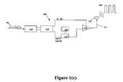
- FIG. 1( c )shows a general block diagram of a transmitter incorporating aspects of the invention.
- FIG. 2shows a transmitter embodiment
- FIGS. 3( a )–( d )show amplifier embodiments.
- Embodiments of the present inventioninclude apparatus, methods and articles of manufacture for transmitting and receiving electromagnetic waves and signals.
- Embodiments of the inventionmay be entirely comprised of hardware, software and/or may be a combination of software and hardware. Accordingly, individual blocks and combinations of blocks in the drawings support combinations of means for performing the specified functions and/or combinations of steps for performing the specified functions.
- Each of the blocks of the drawings, and combinations of blocks of the drawingsmay be embodied in many different ways, as is well known to those of skill in the art.
- SAsegmented amplifier
- baseband I and Q data signalsmay be applied directly to the SA.
- SAsegmented amplifier
- embodiments of the inventionmay also utilize a constant envelope RF signal in power amplification by applying the analog I and Q signals directly to the segments of the SA.
- FIG. 1( a )shows one embodiment of a general transmitter 100 for receiving an input wave 101 and transmitting an output signal 102 using a quadrature based modulation scheme. While described herein in terms of a transmitter, those of ordinary skill in the art will appreciate that the invention may also be used for receivers and tranceivers as well.
- an input wave 101may consist of varying types of intelligence, e.g., voice, data, etc.
- the input wave 101may be analog or digital, and is not limited.
- the transmitted output signal 102may consist of various types of intelligence modulated onto a carrier wave, e.g. voice, data, etc. as is further described below. While the output signal may be analog, a digital output signal may be constructed as well and the invention is not limited.
- signalis used herein to describe an electromagnetic wave that has been modulated in some fashion, usually by the impression of intelligence upon the wave, for example imposing data upon a carrier wave.
- signal and wavein the singular includes the plural (or multiple signals and waves respectively) as often transmitters, receivers and transceivers generate more than one signal and/or wave in the normal course of their operation.
- multiple harmonics of the basebandmight be desirably generated as in amplitude modulation; multiple frequencies might be generated, etc.
- embodiments of the inventionmight be used as well to input and/or output waves, as well as signals, as is further described below.
- Transmitter 100may comprise a baseband processor 115 , signal processor 118 , mixers 105 and 106 , carrier wave source 110 , a combiner 119 , an amplifier system 120 , load line 121 , and an antenna 125 .
- a baseband input wave 101may be inputted into baseband processor 115 , which may generate I and Q data signals (analog or digital) representative of input wave 101 .
- a signal processor 118may be used to further process the I and Q signals, such as correcting the signals for non-linearities produced in power amplifier 120 or to filter unwanted frequency components from the signal.
- the I and Q signalsmay then pass to mixer 105 and 106 along separate channels I and Q respectively.
- Each of the I and Q data signalsmay then be mixed with a carrier wave generated by carrier wave source 110 .
- the signalmay then be recombined at combiner 119 and fed into amplifier 120 .
- Amplifier system 120may be used to drive antenna 125 through load line 121 using the recombined modulated carrier signal, from which the output signal 102 may be transmitted.
- Output signal 102may represent an amplified version of input wave 101 , modulated onto the carrier wave provided by carrier wave source 110 .
- FIG. 1( b )illustrates one embodiment of a general transmitter used to receive an input wave 101 and generate an output signal using a polar based modulation scheme.
- input wave 101may be received by baseband processor 115 , which generate signals representing the amplitude (R) and phase ( ⁇ ) of input wave 101 , which may be analog or digital signals.
- the phase portion of the signal, ⁇may then be passed to a modulator 112 , where it is used to modulate a carrier wave from carrier wave source 110 .
- This modulated carrier signalwhich typically has a substantially constant envelope, may then be inputted to amplifier system 120 .
- the gain or level of amplification of the modulated carrier wave signal by amplifier system 120may be controlled by the amplitude signal (R) in order to use amplifier system 120 to drive antenna 125 through load line 121 with an output signal 102 , which is an amplified version of input wave 101 modulated onto the carrier wave.
- Ramplitude signal
- Thismay be accomplished, for example, by using individual bits of a digital word representing the amplitude portion of input wave 101 to control individual power amplifiers or segments within amplifier system 120 , each of which receives the modulated carrier wave signal.
- FIG. 1( c )illustrates one embodiment of a general transmitter that may be used to generate an output signal using the system of the invention.
- an input wavemay be received by baseband processor 115 , where it may be converted into two or more signals, which, when combined represent input wave 101 .
- I and Q data signalswill be used. Those of ordinary skill in the art will appreciate, however, that the invention is not limited thereto.
- additional signal processingmay or may not be performed by signal processor 118 .
- a signal containing a characteristic of the signals representing input wave 101such as the sign of an I signal and a Q signal, may be passed to a modulator 114 , where this aspect of the signals representing input wave 101 may be used to modulate a carrier wave from a carrier wave source 110 to produce one or more modulated carrier wave signals.
- the modulated carrier wave signal(s)may then be passed to amplifier system 120 . It would be advantageous for modulated carrier wave signal(s) to have a substantially constant envelope in order to utilize non-linear amplification systems in amplifier 120 .
- the amplifiermay comprise any components or circuitry capable of amplifying an electromagnetic wave, such as one or more power amplifiers or transistor segments forming an SA, etc.
- Another characteristic of the signals representing input wave 101such as the magnitude of an signal (
- Amplifier 120may thus be used to drive antenna 125 through load line 121 with an output signal 102 that is an amplified version of input wave 101 modulated onto a carrier wave signal.
- baseband processor 115may include a controller 210 (e.g., an XY constellation generator) that may receive an input wave and generate two or more signals representing the input wave, such as I and Q data signals.
- Controller 210is not limited, but may comprise a digital signal processor in this embodiment, having an analog to digital converter that may digitize the wave into rectangular coordinates of I and Q data signals.
- these I, Q characteristics of the original input wavemay be modulated into digital pulses comprising a digital word quantitized into bits B 1 to Bn, with a Most Significant Bit (“MSB”) to Least Significant Bit (“LSB”).
- MSBMost Significant Bit
- LSBLeast Significant Bit
- the digital wordmay be of varying lengths in various embodiments. In general, the longer the word the greater the accuracy of reproduction of the input wave by the system (i.e, its resolution).
- the digital wordsmay be converted to analog signals and used to provide control for amplification of the modulated signal, in manner to be described further below.
- a differently composed digital wordmay be used, or none at all; that is, characteristics of the input wave may remain in some analog form.
- the signals representing the input wavemay then be transmitted through separate paths or channels to amplifier system 120 .
- I and Q data signalsmay be passed from baseband processor 115 to a signal processor 118 .
- Signal processor 118may include, for example, filter 212 for filtering out unwanted frequency components to perform shaping of the signal pulses.
- filter 212may use polyphase filter banks that have a configurable number of taps and programmable filter coefficients to support different digital modulation schemes, although not limited thereto.
- filter 212may comprise a low-pass filter, such as a finite impulse response (FIR) or an infinite impulse response (IIR) filter.
- FIRfinite impulse response
- IIRinfinite impulse response
- filter 212may comprise a low-pass filter bank, which is comprised of a series of filters F 0 to F n ⁇ l .
- the impulse responses of filters F 0 to F n ⁇ 1may be at h 0 (t) to h n ⁇ 1 (t) respectively.
- one impulse response h(t)may be determined based upon the output to be produced at amplifier 120 that is applied to each of the signal bits.
- the signals representing the input wavemay then be passed through a digital correction system 216 to reduce nonlinearities, such as bowing due to AM/PM distortion, in the resulting signal outputted from amplifier 120 .
- a digital correction system 216may be used.
- digital correction system 216may comprise one or more digital signal processors (that may or may not be part of baseband processor 115 also) that contains an algorithm that uses a look-up table (LUT) containing values based upon a linear approximation of the output from amplifier 120 to correct the signals representing the input wave (e.g., I and Q component signals) to help maintain the linearity of the output signal from power amplifier 120 .
- LUTlook-up table
- the N-bit values of I and Q data signalsmay be translated into new N-bit values that will linearize the resulting output from power amplifier 120 closer to its desired values.
- a correction tablemay comprise 2 N ⁇ 1 (2 N +1) entries, since values for each of the I and Q data signals would comprise 2N bits in this embodiment.
- the actual number of entriesmay be reduced depending on the characteristics of amplifier 120 . The better the characteristics of amplifier 120 , the less phase distortion per state, and the more entries that may be segmented into a smaller number of entries.
- Digital correction system 216may be used to make fine phase and amplitude corrections to the carrier wave signal via phase-locked loop (PLL) 226 and gain pre-stage 230 of carrier wave source 110 .
- Correction signalsmay be computed by digital correction system 216 , for example, based upon I and Q signals that it receives, and passed to PLL 226 and gain pre-stage 230 .
- small phase and amplitude correctionsmay be made to the reference source (f ref ) from an oscillator 246 for the carrier wave (f carrier ) in PLL 226 and to gain pre-stage 230 , as shown in FIG. 2 .
- FIG. 2In the example shown in FIG.
- ⁇ cis the determined correct phase of the signal
- ⁇ icis the incorrect measured phase
- the difference ⁇ c ⁇ icis the amount of the correction that may be applied to PLL 226 .
- r cis the correct magnitude for the signal
- r icis the incorrect measured magnitude
- the ratio r c /r icis the correction amount that may be applied to the carrier wave at gain pre-stage 230 .
- the output I and Q signalsmay be linearized as close as possible to the desired resulting output, and only small amplitude and phase corrections need to be made to the carrier signal.
- digital baseband correctionis typically one-dimensional, being applied to the amplitude aspect of the input wave, and all of the phase correction must be done in the PLL of a phase modulator. This results in a greater sensitivity of polar based systems to phase error, particularly at higher sampling rates.
- each I signal componentmay be passed to a mixer 232 in modulator 114 , where it may be modulated onto a carrier wave produced by oscillator 246 and PLL 226 in carrier wave source 110 .
- Carrier wave oscillator 246may be any source of electromagnetic waves that is capable of producing a signal wave, such as a voltage-controlled oscillator (VCO). In another embodiment this signal source may be a TCXO.
- VCOvoltage-controlled oscillator
- this signal sourcemay be a TCXO.
- the sign portion of a Q signal componentmay be inputted to a mixer 236 within modulator 114 .
- the modulated wave outputted from mixers 232 and 236may each have a substantially constant envelope, i.e., they have no amplitude variations, yet have characteristics of the original input wave. Because the Q data signal is in quadrature with the I data signal, the carrier wave may be phase shifted by ninety degrees using phase shifter 234 .
- Phase shifter 234may comprise any mechanism capable of shifting the phase of the carrier signal wave, such as through the use of delay lines, waveguide elements, microstrips, etc.
- modulator 114is not limited to the embodiment disclosed herein, but may comprise any circuitry and/or components capable of producing one or more modulated carrier wave signals based upon the inputting of a carrier wave and a characteristic of two or more signals that represent the input wave. For example, if a carrier wave of frequency ⁇ c is inputted to modulator 114 , along with the sign ( ⁇ ) of an I and a Q signal representing the input wave, then modulator 114 may output one or more signals, such as +cos( ⁇ c ), ⁇ cos( ⁇ c ), +sin( ⁇ c ), and ⁇ sin( ⁇ c ). This may be accomplished in the above-described manner or any other.
- Another characteristic of the signals that represent the input wave when combinedsuch as the magnitude portion of each I and Q signal component, may be passed through digital to analog converter 222 , for conversion to an analog control signal.
- the converted signalmay also be filtered.
- Each I and Q control signalmay be passed to amplifier 120 for controlling the power outputted therefrom.
- amplifier 120may be an analog segmented amplifier comprising a plurality of amplifying segments 240 .
- Each of the segmentsmay receive a signal from a control component if the control component is on, and so each segment is regulated according to that component.
- the regulationmay be of the bias current to the segments, as is described further below, and so the control component may be referred to as a bias control circuit, and a number of them as a bias network.
- itmay be desired to statically or dynamically allocate one or more control circuits to one or more segments.
- the amplifiermay include disjoint I and Q amplifying sections 324 and 326 .
- the modulated carrier wave(s) from modulator 114( FIG. 2) may be inputted into each section.
- the magnitude control for the I signal componentmay be inputted into the I section 324 and the magnitude control for the Q signal component may be inputted into the Q section 325 .
- Each section 324 , 326may include a plurality of individual power amplifying segments ( 310 – 312 and 314 – 316 , respectively). These may comprise, for example, power amplifiers, although not limited thereto.
- Each of the power amplifying segmentsmay or may not produce an output depending on the magnitude control signal received by it.
- Combining circuit 320is not particularly limited, and may comprise any mechanism for combining the output from each power amplifier, such as by using power transformers, quarter-wave transmission lines, discrete LC components (e.g., Pi-networks), and the like.
- the amplifiermay also contain segmented transistors 330 and 332 , which may serve as potential current sources.
- Each amplifying segment of the transistorsmay or may not act as a current source, because it is regulated via the appropriate analog signal from the I or Q data signal for regulating that control component, and activation of a segment is dependant upon the value of control signal, and concomitant regulation of the appropriate control component.
- the transistors and their segmentsmay be an HBT transistor.
- Other transistorsmay be used as well, such as FET, etc., as well as other current or wave characteristic sources.
- Other componentsmay be interposed as well, e.g., a driver before transistor 400 , a VGA to reduce the drive current to the transistor segments, etc.
- each of the amplifying segmentsmay vary in size. For example, if the overall gain of the amplifier is to be “A”, one segment may be twice the size of the next segment, which in turn may be twice the size of the next segment, and so on until reaching the final segment, where the sum of the gain of all of the segments is equal to A.
- the largest segmentmay be controlled by the analog signal for the magnitude of the I (and/or Q) that correlates to MSB of the original digital signal word, the analog signal representing the next bit to the next largest segment, etc., until the analog signal representing the LSB, which is sent to the smallest segment.
- other embodimentsmay have a different pattern of matching signal to segment.
- other wave characteristicsmay be fed to another source of wave characteristics and so regulate that source.
- FIGS. 3( c ) and 3 ( d )show embodiments of amplifier 120 in which a series of segments may be used.
- a single segmentmaybe used as well.
- the analog amplitude component of each of an I and a Q signalmay be used to control a single segment (or series of segments in an alternating fashion, where the alternating outputs of the segment are combined.
- I and Q analog control signalsmay be filtered together to produce a control signal for a single amplifier segment or series of segments.
- a portion of the signals that represent the input wavemay be used to actuate individual amplifying segments within amplifier 120 to amplify the modulated carrier signal in relation to the original input wave. This produces an output current from amplifier 120 that represents an amplified carrier wave carrying the intelligence contained within the input wave.
- transmitter embodimentsmay proceed with various types of antennas, both active and passive. Additionally, it should be noted that an antenna may not be required in some embodiments, e.g. in wired transmitter, receiver, and/or transceiver embodiments.
- a transmitter, receiver, and transceiver of the inventionmay be specialized for particular input waves, carrier waves and output signals, e.g. various types of cell phones, such as CDMA, CDMA2000, W-CDMA, GSM, TDMA, as well as various other types of devices, both wired and wireless, e.g. Bluetooth, 802.11 a , - b , - g , GPS, radar, 1 ⁇ RTT, radios, GPRS, computers and computer communication devices, handheld devices, etc.
- various types of cell phonessuch as CDMA, CDMA2000, W-CDMA, GSM, TDMA
- various other types of devicese.g. Bluetooth, 802.11 a , - b , - g , GPS, radar, 1 ⁇ RTT, radios, GPRS, computers and computer communication devices, handheld devices, etc.
- GMSKwhich is used in GSM
- GFSKwhich is used in DECT & Bluetooth
- 8-PSKwhich is used in EDGE
- OQPSK & HPSKwhich are used in IS-2000
- p/4 DQPSKwhich is used in TDMA
- OFDMwhich is used in 802.11.
- Various embodimentsmay utilize both analog and digital components insofar as these embodiments manipulate waves and signals requiring both.
- cell phone embodimentsmay utilize both analog and digital components.
- Various types of system architecturesmay be utilized for constructing the embodiments.
- an ASIC compositionmay be used in realizing the various architectures.
- CMOS and/or BiCMOS fabrication techniquesmay be used as well as a combination of both, e.g. a BiCMOS Phase modulator area combined with a CMOS baseband area.
- transistor speedis a concern, and BiCMOS provides faster speed.
- BiCMOSprovides less current drain than an all CMOS configuration.
- the inventionimproves over the systems of the prior art.
- Conventional I/Q modulatorshave been used with linear modulation schemes and amplifiers. Not using such linear modulation eliminates the problem of I/Q imbalance and distortion that occurs when these systems are used.
- Q data in the system of the inventionalso has advantages over other modulation schemes, such as, for example, polar based modulation.
- the inventioneliminates the need for a polar conversion stage and the difficulties associated with the design of a phase modulator module that would be required for interfacing the phase signal to an ASA.
- the bandwidth and quantization requirements for the I and Q signalsare much smaller than those for the amplitude and phase signals used in polar based modulation.
- Power controlmay be accomplished by varying the input power levels to the power amplifier via a voltage-controlled attenuator, along with the base bias voltages on the buffer and I, Q modulator stages.
- the modulation functionis performed at the final stage in the transmit line-up. This allows for a very efficient solution for the overall transmitter as the modulated RF carrier signal applied to all gain blocks of the transmitter will be constant envelope.
Landscapes
- Engineering & Computer Science (AREA)
- Computer Networks & Wireless Communication (AREA)
- Signal Processing (AREA)
- Amplifiers (AREA)
- Transmitters (AREA)
- Digital Transmission Methods That Use Modulated Carrier Waves (AREA)
Abstract
Description
Claims (41)
Priority Applications (3)
| Application Number | Priority Date | Filing Date | Title |
|---|---|---|---|
| US10/606,079US7221915B2 (en) | 2003-06-25 | 2003-06-25 | Electromagnetic wave transmitter, receiver and transceiver systems, methods and articles of manufacture |
| PCT/US2003/031782WO2004034566A1 (en) | 2002-10-08 | 2003-10-07 | Electromagnetic wave transmitter, receiver and transceiver systems, methods and articles of manufacture |
| AU2003275477AAU2003275477A1 (en) | 2002-10-08 | 2003-10-07 | Electromagnetic wave transmitter, receiver and transceiver systems, methods and articles of manufacture |
Applications Claiming Priority (1)
| Application Number | Priority Date | Filing Date | Title |
|---|---|---|---|
| US10/606,079US7221915B2 (en) | 2003-06-25 | 2003-06-25 | Electromagnetic wave transmitter, receiver and transceiver systems, methods and articles of manufacture |
Publications (2)
| Publication Number | Publication Date |
|---|---|
| US20040266359A1 US20040266359A1 (en) | 2004-12-30 |
| US7221915B2true US7221915B2 (en) | 2007-05-22 |
Family
ID=33539981
Family Applications (1)
| Application Number | Title | Priority Date | Filing Date |
|---|---|---|---|
| US10/606,079Expired - Fee RelatedUS7221915B2 (en) | 2002-10-08 | 2003-06-25 | Electromagnetic wave transmitter, receiver and transceiver systems, methods and articles of manufacture |
Country Status (1)
| Country | Link |
|---|---|
| US (1) | US7221915B2 (en) |
Cited By (5)
| Publication number | Priority date | Publication date | Assignee | Title |
|---|---|---|---|---|
| US20070146090A1 (en)* | 2005-12-22 | 2007-06-28 | M/A-Com Eurotec Bv | Apparatus, system, and method for digital base modulation of power amplifier in polar transmitter |
| US20120236965A1 (en)* | 2011-03-16 | 2012-09-20 | Ontario, Canada) | Quadrature communications device with power combiner and related methods |
| US20120236960A1 (en)* | 2011-03-16 | 2012-09-20 | Ontario, Canada) | Quadrature communications device with i antennas and q antennas and related methods |
| US20120236959A1 (en)* | 2011-03-16 | 2012-09-20 | of Ontario, Canada) | Quadrature communications device with i antennas and q antennas and modulated power supply and related methods |
| WO2013086361A1 (en)* | 2011-12-07 | 2013-06-13 | Texas Instruments Incorporated | Transformer power combiner with filter response |
Families Citing this family (8)
| Publication number | Priority date | Publication date | Assignee | Title |
|---|---|---|---|---|
| US7751496B2 (en)* | 2003-06-25 | 2010-07-06 | Pine Valley Investments, Inc. | Electromagnetic wave transmitter, receiver and transceiver systems, methods and articles of manufacture |
| US7221915B2 (en) | 2003-06-25 | 2007-05-22 | M/A-Com, Inc. | Electromagnetic wave transmitter, receiver and transceiver systems, methods and articles of manufacture |
| US7151913B2 (en)* | 2003-06-30 | 2006-12-19 | M/A-Com, Inc. | Electromagnetic wave transmitter, receiver and transceiver systems, methods and articles of manufacture |
| US7027793B2 (en) | 2002-11-15 | 2006-04-11 | Qualcomm Incorporated | Direct conversion with variable amplitude LO signals |
| US7599448B2 (en)* | 2006-02-03 | 2009-10-06 | Pine Valley Investments, Inc. | Multi-mode selectable modulation architecture calibration and power control apparatus, system, and method for radio frequency power amplifier |
| US20070216455A1 (en)* | 2006-03-17 | 2007-09-20 | M/A-Com, Inc. | Partial cascode delay locked loop architecture |
| EP2501094B1 (en)* | 2011-03-16 | 2016-12-07 | BlackBerry Limited | Quadrature communications device with i antennas and q antennas and related methods |
| EP2501093B1 (en)* | 2011-03-16 | 2019-06-05 | BlackBerry Limited | Quadrature communications device with I antennas and Q antennas and modulated power supply and related methods |
Citations (66)
| Publication number | Priority date | Publication date | Assignee | Title |
|---|---|---|---|---|
| GB363535A (en) | 1930-02-12 | 1931-12-24 | Budd Wheel Co | Improvements in or relating to wheels |
| US3896395A (en) | 1974-07-18 | 1975-07-22 | Bell Telephone Labor Inc | Linear amplification using quantized envelope components to phase reverse modulate quadrature reference signals |
| US5056109A (en) | 1989-11-07 | 1991-10-08 | Qualcomm, Inc. | Method and apparatus for controlling transmission power in a cdma cellular mobile telephone system |
| US5066923A (en) | 1990-10-31 | 1991-11-19 | Motorola, Inc. | Linear transmitter training method and apparatus |
| US5249201A (en) | 1991-02-01 | 1993-09-28 | Mst, Inc. | Transmission of multiple carrier signals in a nonlinear system |
| US5257283A (en) | 1989-11-07 | 1993-10-26 | Qualcomm Incorporated | Spread spectrum transmitter power control method and system |
| US5265119A (en) | 1989-11-07 | 1993-11-23 | Qualcomm Incorporated | Method and apparatus for controlling transmission power in a CDMA cellular mobile telephone system |
| US5267262A (en) | 1989-11-07 | 1993-11-30 | Qualcomm Incorporated | Transmitter power control system |
| WO1994024759A1 (en) | 1993-04-14 | 1994-10-27 | Acrodyne Industries, Inc. | Balanced modulator-transmitter |
| US5396516A (en) | 1993-02-22 | 1995-03-07 | Qualcomm Incorporated | Method and system for the dynamic modification of control paremeters in a transmitter power control system |
| US5420536A (en) | 1993-03-16 | 1995-05-30 | Victoria University Of Technology | Linearized power amplifier |
| US5452473A (en) | 1994-02-28 | 1995-09-19 | Qualcomm Incorporated | Reverse link, transmit power correction and limitation in a radiotelephone system |
| US5485486A (en) | 1989-11-07 | 1996-01-16 | Qualcomm Incorporated | Method and apparatus for controlling transmission power in a CDMA cellular mobile telephone system |
| US5507017A (en) | 1993-09-29 | 1996-04-09 | Linear Modulation Technology Limited | Control of attenuation and amplification in foward and feedback paths for power control for cartesian amplifiers |
| US5661434A (en) | 1995-05-12 | 1997-08-26 | Fujitsu Compound Semiconductor, Inc. | High efficiency multiple power level amplifier circuit |
| US5703902A (en) | 1995-06-16 | 1997-12-30 | Qualcomm Incorporated | Method and apparatus for determining signal strength in a variable data rate system |
| US5758269A (en) | 1995-03-30 | 1998-05-26 | Lucent Technologies Inc. | High-efficient configurable power amplifier for use in a portable unit |
| US5757858A (en) | 1994-12-23 | 1998-05-26 | Qualcomm Incorporated | Dual-mode digital FM communication system |
| US5861773A (en) | 1995-07-06 | 1999-01-19 | Sgs-Thomson Microelectronics S.A. | Circuit for detecting the locked condition of PSK or QAM |
| US5894496A (en) | 1996-09-16 | 1999-04-13 | Ericsson Inc. | Method and apparatus for detecting and compensating for undesired phase shift in a radio transceiver |
| US5901346A (en) | 1996-12-11 | 1999-05-04 | Motorola, Inc. | Method and apparatus utilizing a compensated multiple output signal source |
| US5903554A (en) | 1996-09-27 | 1999-05-11 | Qualcomm Incorporation | Method and apparatus for measuring link quality in a spread spectrum communication system |
| US5974041A (en) | 1995-12-27 | 1999-10-26 | Qualcomm Incorporated | Efficient parallel-stage power amplifier |
| US6011437A (en)* | 1998-05-04 | 2000-01-04 | Marvell Technology Group, Ltd. | High precision, high bandwidth variable gain amplifier and method |
| US6075974A (en) | 1996-11-20 | 2000-06-13 | Qualcomm Inc. | Method and apparatus for adjusting thresholds and measurements of received signals by anticipating power control commands yet to be executed |
| WO2000041371A2 (en) | 1999-01-07 | 2000-07-13 | Ericsson, Inc. | Power i-q modulation systems and methods using predistortion circuit |
| EP1035701A1 (en) | 1999-03-08 | 2000-09-13 | Motorola, Inc. | Modulator using envelope elimination and restoration by means of look-up tables |
| US6178313B1 (en) | 1998-12-31 | 2001-01-23 | Nokia Mobile Phones Limited | Control of gain and power consumption in a power amplifier |
| US6185432B1 (en) | 1997-10-13 | 2001-02-06 | Qualcomm Incorporated | System and method for selecting power control modes |
| US6191653B1 (en) | 1998-11-18 | 2001-02-20 | Ericsson Inc. | Circuit and method for linearizing amplitude modulation in a power amplifier |
| US6194963B1 (en)* | 1998-11-18 | 2001-02-27 | Ericsson Inc. | Circuit and method for I/Q modulation with independent, high efficiency amplitude modulation |
| US6259928B1 (en) | 1997-10-13 | 2001-07-10 | Qualcomm Inc. | System and method for optimized power control |
| US6272336B1 (en) | 1998-12-30 | 2001-08-07 | Samsung Electronics Co., Ltd. | Traffic-weighted closed loop power detection system for use with an RF power amplifier and method of operation |
| US6295442B1 (en) | 1998-12-07 | 2001-09-25 | Ericsson Inc. | Amplitude modulation to phase modulation cancellation method in an RF amplifier |
| US6308057B1 (en) | 1998-01-16 | 2001-10-23 | Oki Electric Industry Co., Ltd. | Radio receiver having compensation for direct current offset |
| US6313703B1 (en) | 1998-06-19 | 2001-11-06 | Datum Telegraphic, Inc | Use of antiphase signals for predistortion training within an amplifier system |
| US6320913B1 (en) | 1997-06-23 | 2001-11-20 | Nec Corporation | Circuit and method for controlling transmission amplifiers |
| US6330462B1 (en) | 1997-07-01 | 2001-12-11 | Qualcomm Incorporated | Method and apparatus for pre-transmission power control using lower rate for high rate communication |
| EP1170915A1 (en) | 1999-03-31 | 2002-01-09 | Kabushiki Kaisha Toshiba | Signal modulation circuit and method for signal modulation |
| US6351650B1 (en) | 1999-01-28 | 2002-02-26 | Qualcomm Incorporated | System and method for forward link power balancing in a wireless communication system |
| US6370109B1 (en) | 1999-03-10 | 2002-04-09 | Qualcomm Incorporated | CDMA signal power control using quadrature signal calculations |
| US6411655B1 (en)* | 1998-12-18 | 2002-06-25 | Ericsson Inc. | Systems and methods for converting a stream of complex numbers into an amplitude and phase-modulated radio power signal |
| US6421327B1 (en) | 1999-06-28 | 2002-07-16 | Qualcomm Incorporated | Method and apparatus for controlling transmission energy in a communication system employing orthogonal transmit diversity |
| US6438360B1 (en) | 1999-07-22 | 2002-08-20 | Motorola, Inc. | Amplifier system with load control to produce an amplitude envelope |
| US6449465B1 (en) | 1999-12-20 | 2002-09-10 | Motorola, Inc. | Method and apparatus for linear amplification of a radio frequency signal |
| US6466628B1 (en) | 1998-04-18 | 2002-10-15 | Lucent Technologies Inc. | Technique for effectively rendering power amplification and control in wireless communications |
| US6490460B1 (en) | 1998-12-01 | 2002-12-03 | Qualcomm Incorporated | Forward and reverse link power control using position and mobility information |
| US20020196864A1 (en) | 2001-06-19 | 2002-12-26 | Booth Richard W.D. | Hybrid polar modulator differential phase cartesian feedback correction circuit for power amplifier linearization |
| US20030073419A1 (en) | 2001-10-10 | 2003-04-17 | Zarlink Semiconductor Limited | Power control in polar loop transmitters |
| US6628165B1 (en) | 2000-11-07 | 2003-09-30 | Linear Technology Corporation | Power controllers for amplitude modulation |
| US6633199B2 (en) | 2000-12-15 | 2003-10-14 | Nokia Corporation | Amplifier circuit, radio transmitter, method and use |
| US6653909B2 (en) | 2000-12-15 | 2003-11-25 | Nokia Corporation | Digital signals, radio transmitter circuits and method |
| US20030223510A1 (en) | 2002-05-31 | 2003-12-04 | Noriyuki Kurakami | Semiconductor integrated circuit for communication, radio-communications apparatus, and transmission starting method |
| US6690233B2 (en) | 2000-12-21 | 2004-02-10 | Tropian, Inc. | Efficient, precise RF modulation using multiple amplifier stages |
| US6701134B1 (en) | 2002-11-05 | 2004-03-02 | Rf Micro Devices, Inc. | Increased dynamic range for power amplifiers used with polar modulation |
| US6714071B1 (en) | 2001-06-25 | 2004-03-30 | Nortel Networks Limited | Gate modulation for high power amplifiers |
| US20040192369A1 (en) | 2002-08-08 | 2004-09-30 | Magnus Nilsson | Method and apparatus for reducing dynamic range of a power amplifier |
| US20040266359A1 (en) | 2003-06-25 | 2004-12-30 | M/A-Com, Inc. | Electromagnetic wave transmitter, receiver and transceiver systems, methods and articles of manufacture |
| US20040264583A1 (en) | 2003-06-30 | 2004-12-30 | M/A-Com, Inc. | Electromagnetic wave transmitter, receiver and transceiver systems, methods and articles of manufacture |
| US20050030104A1 (en) | 2003-08-07 | 2005-02-10 | Ntt Docomo, Inc. | Power amplifier |
| US6865396B2 (en) | 1998-11-26 | 2005-03-08 | Nokia Corporation | System and method of power control using a modulated signal |
| US6870435B2 (en)* | 2003-06-30 | 2005-03-22 | Mia-Com, Inc. | Electromagnetic wave transmitter, receiver and transceiver systems, methods and articles of manufacture |
| US20050226340A1 (en) | 2003-06-25 | 2005-10-13 | M/A-Com, Inc. | Electromagnetic wave transmitter, receiver and transceiver systems, methods and articles of manufacturre |
| US6973394B2 (en)* | 2001-01-08 | 2005-12-06 | Alcatel | Device for remote power feeding a terminal in a telecommunication network, and a concentrator and a repreater including the device |
| US7002417B2 (en) | 2003-03-21 | 2006-02-21 | Nokia Corporation | RC and SC filter compensation in a radio transceiver |
| US7062236B2 (en) | 2000-12-22 | 2006-06-13 | Nokia Corporation | Transmitter circuits |
- 2003
- 2003-06-25USUS10/606,079patent/US7221915B2/ennot_activeExpired - Fee Related
Patent Citations (71)
| Publication number | Priority date | Publication date | Assignee | Title |
|---|---|---|---|---|
| GB363535A (en) | 1930-02-12 | 1931-12-24 | Budd Wheel Co | Improvements in or relating to wheels |
| US3896395A (en) | 1974-07-18 | 1975-07-22 | Bell Telephone Labor Inc | Linear amplification using quantized envelope components to phase reverse modulate quadrature reference signals |
| US5485486A (en) | 1989-11-07 | 1996-01-16 | Qualcomm Incorporated | Method and apparatus for controlling transmission power in a CDMA cellular mobile telephone system |
| US5056109A (en) | 1989-11-07 | 1991-10-08 | Qualcomm, Inc. | Method and apparatus for controlling transmission power in a cdma cellular mobile telephone system |
| US5257283A (en) | 1989-11-07 | 1993-10-26 | Qualcomm Incorporated | Spread spectrum transmitter power control method and system |
| US5265119A (en) | 1989-11-07 | 1993-11-23 | Qualcomm Incorporated | Method and apparatus for controlling transmission power in a CDMA cellular mobile telephone system |
| US5267262A (en) | 1989-11-07 | 1993-11-30 | Qualcomm Incorporated | Transmitter power control system |
| US5066923A (en) | 1990-10-31 | 1991-11-19 | Motorola, Inc. | Linear transmitter training method and apparatus |
| US5249201A (en) | 1991-02-01 | 1993-09-28 | Mst, Inc. | Transmission of multiple carrier signals in a nonlinear system |
| US5396516A (en) | 1993-02-22 | 1995-03-07 | Qualcomm Incorporated | Method and system for the dynamic modification of control paremeters in a transmitter power control system |
| US5420536A (en) | 1993-03-16 | 1995-05-30 | Victoria University Of Technology | Linearized power amplifier |
| WO1994024759A1 (en) | 1993-04-14 | 1994-10-27 | Acrodyne Industries, Inc. | Balanced modulator-transmitter |
| US5507017A (en) | 1993-09-29 | 1996-04-09 | Linear Modulation Technology Limited | Control of attenuation and amplification in foward and feedback paths for power control for cartesian amplifiers |
| US5452473A (en) | 1994-02-28 | 1995-09-19 | Qualcomm Incorporated | Reverse link, transmit power correction and limitation in a radiotelephone system |
| US5590408A (en) | 1994-02-28 | 1996-12-31 | Qualcomm Incorporated | Reverse link, transmit power correction and limitation in a radiotelephone system |
| US5655220A (en) | 1994-02-28 | 1997-08-05 | Qualcomm Incorporated | Reverse link, transmit power correction and limitation in a radiotelephone system |
| US5757858A (en) | 1994-12-23 | 1998-05-26 | Qualcomm Incorporated | Dual-mode digital FM communication system |
| US5758269A (en) | 1995-03-30 | 1998-05-26 | Lucent Technologies Inc. | High-efficient configurable power amplifier for use in a portable unit |
| US5661434A (en) | 1995-05-12 | 1997-08-26 | Fujitsu Compound Semiconductor, Inc. | High efficiency multiple power level amplifier circuit |
| US5703902A (en) | 1995-06-16 | 1997-12-30 | Qualcomm Incorporated | Method and apparatus for determining signal strength in a variable data rate system |
| US5861773A (en) | 1995-07-06 | 1999-01-19 | Sgs-Thomson Microelectronics S.A. | Circuit for detecting the locked condition of PSK or QAM |
| US5974041A (en) | 1995-12-27 | 1999-10-26 | Qualcomm Incorporated | Efficient parallel-stage power amplifier |
| US5894496A (en) | 1996-09-16 | 1999-04-13 | Ericsson Inc. | Method and apparatus for detecting and compensating for undesired phase shift in a radio transceiver |
| US5903554A (en) | 1996-09-27 | 1999-05-11 | Qualcomm Incorporation | Method and apparatus for measuring link quality in a spread spectrum communication system |
| US6075974A (en) | 1996-11-20 | 2000-06-13 | Qualcomm Inc. | Method and apparatus for adjusting thresholds and measurements of received signals by anticipating power control commands yet to be executed |
| US6374085B1 (en) | 1996-11-20 | 2002-04-16 | Qualcomm Incorporated | Method and apparatus for adjusting thresholds and measurements of received signals by anticipating power control commands yet to be executed |
| US5901346A (en) | 1996-12-11 | 1999-05-04 | Motorola, Inc. | Method and apparatus utilizing a compensated multiple output signal source |
| US6320913B1 (en) | 1997-06-23 | 2001-11-20 | Nec Corporation | Circuit and method for controlling transmission amplifiers |
| US6330462B1 (en) | 1997-07-01 | 2001-12-11 | Qualcomm Incorporated | Method and apparatus for pre-transmission power control using lower rate for high rate communication |
| US6185432B1 (en) | 1997-10-13 | 2001-02-06 | Qualcomm Incorporated | System and method for selecting power control modes |
| US6259928B1 (en) | 1997-10-13 | 2001-07-10 | Qualcomm Inc. | System and method for optimized power control |
| US6308057B1 (en) | 1998-01-16 | 2001-10-23 | Oki Electric Industry Co., Ltd. | Radio receiver having compensation for direct current offset |
| US6466628B1 (en) | 1998-04-18 | 2002-10-15 | Lucent Technologies Inc. | Technique for effectively rendering power amplification and control in wireless communications |
| US6011437A (en)* | 1998-05-04 | 2000-01-04 | Marvell Technology Group, Ltd. | High precision, high bandwidth variable gain amplifier and method |
| US6313703B1 (en) | 1998-06-19 | 2001-11-06 | Datum Telegraphic, Inc | Use of antiphase signals for predistortion training within an amplifier system |
| US6194963B1 (en)* | 1998-11-18 | 2001-02-27 | Ericsson Inc. | Circuit and method for I/Q modulation with independent, high efficiency amplitude modulation |
| US6191653B1 (en) | 1998-11-18 | 2001-02-20 | Ericsson Inc. | Circuit and method for linearizing amplitude modulation in a power amplifier |
| US6865396B2 (en) | 1998-11-26 | 2005-03-08 | Nokia Corporation | System and method of power control using a modulated signal |
| US6490460B1 (en) | 1998-12-01 | 2002-12-03 | Qualcomm Incorporated | Forward and reverse link power control using position and mobility information |
| US6295442B1 (en) | 1998-12-07 | 2001-09-25 | Ericsson Inc. | Amplitude modulation to phase modulation cancellation method in an RF amplifier |
| US6411655B1 (en)* | 1998-12-18 | 2002-06-25 | Ericsson Inc. | Systems and methods for converting a stream of complex numbers into an amplitude and phase-modulated radio power signal |
| US6272336B1 (en) | 1998-12-30 | 2001-08-07 | Samsung Electronics Co., Ltd. | Traffic-weighted closed loop power detection system for use with an RF power amplifier and method of operation |
| US6178313B1 (en) | 1998-12-31 | 2001-01-23 | Nokia Mobile Phones Limited | Control of gain and power consumption in a power amplifier |
| WO2000041371A2 (en) | 1999-01-07 | 2000-07-13 | Ericsson, Inc. | Power i-q modulation systems and methods using predistortion circuit |
| US6181199B1 (en) | 1999-01-07 | 2001-01-30 | Ericsson Inc. | Power IQ modulation systems and methods |
| US6351650B1 (en) | 1999-01-28 | 2002-02-26 | Qualcomm Incorporated | System and method for forward link power balancing in a wireless communication system |
| EP1035701A1 (en) | 1999-03-08 | 2000-09-13 | Motorola, Inc. | Modulator using envelope elimination and restoration by means of look-up tables |
| US6370109B1 (en) | 1999-03-10 | 2002-04-09 | Qualcomm Incorporated | CDMA signal power control using quadrature signal calculations |
| EP1170915A1 (en) | 1999-03-31 | 2002-01-09 | Kabushiki Kaisha Toshiba | Signal modulation circuit and method for signal modulation |
| US6914943B2 (en)* | 1999-03-31 | 2005-07-05 | Kabushiki Kaisha Toshiba | Signal modulation circuit and signal modulation method |
| US6421327B1 (en) | 1999-06-28 | 2002-07-16 | Qualcomm Incorporated | Method and apparatus for controlling transmission energy in a communication system employing orthogonal transmit diversity |
| US6438360B1 (en) | 1999-07-22 | 2002-08-20 | Motorola, Inc. | Amplifier system with load control to produce an amplitude envelope |
| US6449465B1 (en) | 1999-12-20 | 2002-09-10 | Motorola, Inc. | Method and apparatus for linear amplification of a radio frequency signal |
| US6628165B1 (en) | 2000-11-07 | 2003-09-30 | Linear Technology Corporation | Power controllers for amplitude modulation |
| US6633199B2 (en) | 2000-12-15 | 2003-10-14 | Nokia Corporation | Amplifier circuit, radio transmitter, method and use |
| US6653909B2 (en) | 2000-12-15 | 2003-11-25 | Nokia Corporation | Digital signals, radio transmitter circuits and method |
| US6690233B2 (en) | 2000-12-21 | 2004-02-10 | Tropian, Inc. | Efficient, precise RF modulation using multiple amplifier stages |
| US7062236B2 (en) | 2000-12-22 | 2006-06-13 | Nokia Corporation | Transmitter circuits |
| US6973394B2 (en)* | 2001-01-08 | 2005-12-06 | Alcatel | Device for remote power feeding a terminal in a telecommunication network, and a concentrator and a repreater including the device |
| US20020196864A1 (en) | 2001-06-19 | 2002-12-26 | Booth Richard W.D. | Hybrid polar modulator differential phase cartesian feedback correction circuit for power amplifier linearization |
| US6714071B1 (en) | 2001-06-25 | 2004-03-30 | Nortel Networks Limited | Gate modulation for high power amplifiers |
| US20030073419A1 (en) | 2001-10-10 | 2003-04-17 | Zarlink Semiconductor Limited | Power control in polar loop transmitters |
| US20030223510A1 (en) | 2002-05-31 | 2003-12-04 | Noriyuki Kurakami | Semiconductor integrated circuit for communication, radio-communications apparatus, and transmission starting method |
| US20040192369A1 (en) | 2002-08-08 | 2004-09-30 | Magnus Nilsson | Method and apparatus for reducing dynamic range of a power amplifier |
| US6701134B1 (en) | 2002-11-05 | 2004-03-02 | Rf Micro Devices, Inc. | Increased dynamic range for power amplifiers used with polar modulation |
| US7002417B2 (en) | 2003-03-21 | 2006-02-21 | Nokia Corporation | RC and SC filter compensation in a radio transceiver |
| US20040266359A1 (en) | 2003-06-25 | 2004-12-30 | M/A-Com, Inc. | Electromagnetic wave transmitter, receiver and transceiver systems, methods and articles of manufacture |
| US20050226340A1 (en) | 2003-06-25 | 2005-10-13 | M/A-Com, Inc. | Electromagnetic wave transmitter, receiver and transceiver systems, methods and articles of manufacturre |
| US20040264583A1 (en) | 2003-06-30 | 2004-12-30 | M/A-Com, Inc. | Electromagnetic wave transmitter, receiver and transceiver systems, methods and articles of manufacture |
| US6870435B2 (en)* | 2003-06-30 | 2005-03-22 | Mia-Com, Inc. | Electromagnetic wave transmitter, receiver and transceiver systems, methods and articles of manufacture |
| US20050030104A1 (en) | 2003-08-07 | 2005-02-10 | Ntt Docomo, Inc. | Power amplifier |
Cited By (11)
| Publication number | Priority date | Publication date | Assignee | Title |
|---|---|---|---|---|
| US20070146090A1 (en)* | 2005-12-22 | 2007-06-28 | M/A-Com Eurotec Bv | Apparatus, system, and method for digital base modulation of power amplifier in polar transmitter |
| US20070247253A1 (en)* | 2005-12-22 | 2007-10-25 | Eoin Carey | Apparatus, system, and method for digital modulation of power amplifier in polar transmitter |
| US8884714B2 (en)* | 2005-12-22 | 2014-11-11 | Pine Valley Investments, Inc. | Apparatus, system, and method for digital base modulation of power amplifier in polar transmitter |
| US20120236965A1 (en)* | 2011-03-16 | 2012-09-20 | Ontario, Canada) | Quadrature communications device with power combiner and related methods |
| US20120236960A1 (en)* | 2011-03-16 | 2012-09-20 | Ontario, Canada) | Quadrature communications device with i antennas and q antennas and related methods |
| US20120236959A1 (en)* | 2011-03-16 | 2012-09-20 | of Ontario, Canada) | Quadrature communications device with i antennas and q antennas and modulated power supply and related methods |
| US8553802B2 (en)* | 2011-03-16 | 2013-10-08 | Blackberry Limited | Quadrature communications device with I antennas and Q antennas and modulated power supply and related methods |
| US8588330B2 (en)* | 2011-03-16 | 2013-11-19 | Blackberry Limited | Quadrature communications device with I antennas and Q antennas and related methods |
| US8594233B2 (en)* | 2011-03-16 | 2013-11-26 | Blackberry Limited | Quadrature communications device with power combiner and related methods |
| WO2013086361A1 (en)* | 2011-12-07 | 2013-06-13 | Texas Instruments Incorporated | Transformer power combiner with filter response |
| US8654867B2 (en) | 2011-12-07 | 2014-02-18 | Texas Instruments Incorporated | Transformer power combiner with filter response |
Also Published As
| Publication number | Publication date |
|---|---|
| US20040266359A1 (en) | 2004-12-30 |
Similar Documents
| Publication | Publication Date | Title |
|---|---|---|
| US7151913B2 (en) | Electromagnetic wave transmitter, receiver and transceiver systems, methods and articles of manufacture | |
| US7751496B2 (en) | Electromagnetic wave transmitter, receiver and transceiver systems, methods and articles of manufacture | |
| US7343138B2 (en) | Compensating for load pull in electromagentic signal propagation using adaptive impedance matching | |
| US6737914B2 (en) | Removing effects of gain and phase mismatch in a linear amplification with nonlinear components (LINC) system | |
| US7792214B2 (en) | Polar modulation transmitter circuit and communications device | |
| CN101331728B (en) | Transmission circuit and communication device using the transmission circuit | |
| US7023292B2 (en) | Polar modulation using amplitude modulated quadrature signals | |
| JPH07183729A (en) | Power amplifier | |
| US7254186B2 (en) | Electromagnetic wave transmitter, receiver and transceiver systems, methods and articles of manufacture | |
| US7221915B2 (en) | Electromagnetic wave transmitter, receiver and transceiver systems, methods and articles of manufacture | |
| US6870435B2 (en) | Electromagnetic wave transmitter, receiver and transceiver systems, methods and articles of manufacture | |
| US9059661B2 (en) | Variable-size mixer for high gain range transmitter | |
| US7502422B2 (en) | Electromagnetic wave transmitter systems, methods and articles of manufacture | |
| US6903619B2 (en) | Electromagnetic wave transmitter systems, methods and articles of manufacture | |
| US7356091B2 (en) | Apparatus, methods and articles of manufacture for signal propagation using unwrapped phase | |
| JP2007104007A (en) | Quadrature modulator and vector correction method in quadrature modulator | |
| WO2004036737A2 (en) | Transmitter | |
| WO2004034603A2 (en) | Transmitter and methods of transmission using separate phase and amplitude modulators | |
| WO2004034566A1 (en) | Electromagnetic wave transmitter, receiver and transceiver systems, methods and articles of manufacture | |
| WO2004034658A2 (en) | Method of digital modulation and corresponding transmitter | |
| WO2004034596A2 (en) | Method and apparatus for transmission using digital modulator | |
| WO2004034667A2 (en) | Electromagnetic wave trasmitter systems, methods and articles of manufacture | |
| EP1750411B1 (en) | Electromagnetic wave transmitter systems, methods and articles of manufacture | |
| WO2004034659A2 (en) | Method and apparatus for digital modulation using a cordic algorithm |
Legal Events
| Date | Code | Title | Description |
|---|---|---|---|
| AS | Assignment | Owner name:M/A-COM, INC., MASSACHUSETTS Free format text:ASSIGNMENT OF ASSIGNORS INTEREST;ASSIGNOR:TRIPP, JEFFREY WILLIAM;REEL/FRAME:014666/0716 Effective date:20031007 | |
| AS | Assignment | Owner name:M/A-COM, INC., MASSACHUSETTS Free format text:ASSIGNMENT OF ASSIGNORS INTEREST;ASSIGNOR:AHMED, WALID KHAIRY MOHAMED;REEL/FRAME:019148/0868 Effective date:20030617 | |
| AS | Assignment | Owner name:PINE VALLEY INVESTMENTS, INC., NEVADA Free format text:ASSIGNMENT OF ASSIGNORS INTEREST;ASSIGNORS:TYCO ELECTRONICS GROUP S.A.;TYCO ELECTRONICS CORPORATION;THE WHITAKER CORPORATION;AND OTHERS;REEL/FRAME:023065/0269 Effective date:20090529 Owner name:PINE VALLEY INVESTMENTS, INC.,NEVADA Free format text:ASSIGNMENT OF ASSIGNORS INTEREST;ASSIGNORS:TYCO ELECTRONICS GROUP S.A.;TYCO ELECTRONICS CORPORATION;THE WHITAKER CORPORATION;AND OTHERS;REEL/FRAME:023065/0269 Effective date:20090529 | |
| FPAY | Fee payment | Year of fee payment:4 | |
| REMI | Maintenance fee reminder mailed | ||
| LAPS | Lapse for failure to pay maintenance fees | ||
| STCH | Information on status: patent discontinuation | Free format text:PATENT EXPIRED DUE TO NONPAYMENT OF MAINTENANCE FEES UNDER 37 CFR 1.362 | |
| FP | Lapsed due to failure to pay maintenance fee | Effective date:20150522 |