US7221017B2 - Memory utilizing oxide-conductor nanolaminates - Google Patents
Memory utilizing oxide-conductor nanolaminatesDownload PDFInfo
- Publication number
- US7221017B2 US7221017B2US10/191,336US19133602AUS7221017B2US 7221017 B2US7221017 B2US 7221017B2US 19133602 AUS19133602 AUS 19133602AUS 7221017 B2US7221017 B2US 7221017B2
- Authority
- US
- United States
- Prior art keywords
- floating gate
- oxide
- conductor
- gate transistor
- nanolaminate layers
- Prior art date
- Legal status (The legal status is an assumption and is not a legal conclusion. Google has not performed a legal analysis and makes no representation as to the accuracy of the status listed.)
- Expired - Fee Related
Links
Images


Classifications
- G—PHYSICS
- G11—INFORMATION STORAGE
- G11C—STATIC STORES
- G11C11/00—Digital stores characterised by the use of particular electric or magnetic storage elements; Storage elements therefor
- G11C11/56—Digital stores characterised by the use of particular electric or magnetic storage elements; Storage elements therefor using storage elements with more than two stable states represented by steps, e.g. of voltage, current, phase, frequency
- G11C11/5671—Digital stores characterised by the use of particular electric or magnetic storage elements; Storage elements therefor using storage elements with more than two stable states represented by steps, e.g. of voltage, current, phase, frequency using charge trapping in an insulator
- H—ELECTRICITY
- H10—SEMICONDUCTOR DEVICES; ELECTRIC SOLID-STATE DEVICES NOT OTHERWISE PROVIDED FOR
- H10B—ELECTRONIC MEMORY DEVICES
- H10B69/00—Erasable-and-programmable ROM [EPROM] devices not provided for in groups H10B41/00 - H10B63/00, e.g. ultraviolet erasable-and-programmable ROM [UVEPROM] devices
- H—ELECTRICITY
- H10—SEMICONDUCTOR DEVICES; ELECTRIC SOLID-STATE DEVICES NOT OTHERWISE PROVIDED FOR
- H10D—INORGANIC ELECTRIC SEMICONDUCTOR DEVICES
- H10D30/00—Field-effect transistors [FET]
- H10D30/60—Insulated-gate field-effect transistors [IGFET]
- H10D30/68—Floating-gate IGFETs
- H10D30/681—Floating-gate IGFETs having only two programming levels
- H10D30/684—Floating-gate IGFETs having only two programming levels programmed by hot carrier injection
- H10D30/685—Floating-gate IGFETs having only two programming levels programmed by hot carrier injection from the channel
- H—ELECTRICITY
- H10—SEMICONDUCTOR DEVICES; ELECTRIC SOLID-STATE DEVICES NOT OTHERWISE PROVIDED FOR
- H10D—INORGANIC ELECTRIC SEMICONDUCTOR DEVICES
- H10D30/00—Field-effect transistors [FET]
- H10D30/60—Insulated-gate field-effect transistors [IGFET]
- H10D30/68—Floating-gate IGFETs
- H10D30/6891—Floating-gate IGFETs characterised by the shapes, relative sizes or dispositions of the floating gate electrode
- H10D30/6893—Floating-gate IGFETs characterised by the shapes, relative sizes or dispositions of the floating gate electrode wherein the floating gate has multiple non-connected parts, e.g. multi-particle floating gate
- G—PHYSICS
- G11—INFORMATION STORAGE
- G11C—STATIC STORES
- G11C16/00—Erasable programmable read-only memories
- G11C16/02—Erasable programmable read-only memories electrically programmable
- G11C16/04—Erasable programmable read-only memories electrically programmable using variable threshold transistors, e.g. FAMOS
- G11C16/0408—Erasable programmable read-only memories electrically programmable using variable threshold transistors, e.g. FAMOS comprising cells containing floating gate transistors
- G11C16/0416—Erasable programmable read-only memories electrically programmable using variable threshold transistors, e.g. FAMOS comprising cells containing floating gate transistors comprising cells containing a single floating gate transistor and no select transistor, e.g. UV EPROM
Definitions
- the present inventionrelates generally to semiconductor integrated circuits and, more particularly, to memory utilizing oxide-conductor nanolaminates.
- DRAMdynamic random access memory
- MOSFETmetal oxide semiconducting field effect transistor
- a conventional horizontal floating gate transistor structureincludes a source region and a drain region separated by a channel region in a horizontal substrate.
- a floating gateis separated by a thin tunnel gate oxide.
- the structureis programmed by storing a charge on the floating gate.
- a control gateis separated from the floating gate by an intergate dielectric.
- a charge stored on the floating gateeffects the conductivity of the cell when a read voltage potential is applied to the control gate. The state of cell can thus be determined by sensing a change in the device conductivity between the programmed and un-programmed states.
- Multilayer insulatorshave been previously employed in memory devices.
- the devices in the above referencesemployed oxide-tungsten oxide-oxide layers.
- Other previously described structures describedhave employed charge-trapping layers implanted into graded layer insulator structures.
- Flash memories based on electron trappingare well known and commonly used electronic components. Recently NAND flash memory cells have become common in applications requiring high storage density while NOR flash memory cells are used in applications requiring high access and read speeds. NAND flash memories have a higher density because 16 or more devices are placed in series, this increases density at the expense of speed.
- This disclosuredescribes a flash memory device, programmable logic array device or memory address and decode correction device with an oxide-conductor nanolaminate floating gate rather than a conventional polysilicon floating gate.
- an embodiment of the present inventionincludes a floating gate transistor utilizing oxide-conductor nanolaminates.
- the floating gate transistorincludes a first source/drain region, a second source/drain region, and a channel region therebetween.
- a floating gateis separated from the channel region by a first gate oxide.
- the floating gateincludes oxide-conductor nanolaminate layers to trap charge in potential wells formed by different electron affinities of the oxide-conductor nanolaminate layers.
- FIG. 1Ais a block diagram of a metal oxide semiconductor field effect floating gate transistor (MOSFET) in a substrate according to the teachings of the prior art.
- MOSFETmetal oxide semiconductor field effect floating gate transistor
- FIG. 1Billustrates the MOSFET of FIG. 1A operated in the forward direction showing some degree of device degradation due to electrons being trapped in the gate oxide near the drain region over gradual use.
- FIG. 1Cis a graph showing the square root of the current signal (Ids) taken at the drain region of the conventional MOSFET versus the voltage potential (VGS) established between the gate and the source region.
- FIG. 2Ais a diagram of an embodiment for a programmed floating gate transistor, having oxide-conductor nanolaminate layers, which can be used as a floating gate transistor cell according to the teachings of the present invention.
- FIG. 2Bis a diagram suitable for explaining a method embodiment by which a floating gate transistor, having oxide-conductor nanolaminate layers, can be programmed to achieve the embodiments of the present invention.
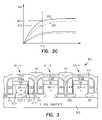
- FIG. 2Cis a graph plotting the current signal (Ids) detected at the drain region versus a voltage potential, or drain voltage, (VDS) set up between the drain region and the source region (Ids vs. VDS).
- FIG. 3illustrates a portion of an embodiment of a memory array according to the teachings of the present invention.
- FIG. 4illustrates an embodiment for an electrical equivalent circuit for the portion of the memory array shown in FIG. 3 .
- FIG. 5illustrates an energy band diagram for an embodiment of a gate stack according to the teachings of the present invention.
- FIG. 6is a graph which plots electron affinity versus the energy bandgap for various insulators.
- FIGS. 7A–7Billustrates an embodiment for the operation of a floating gate transistor cell having oxide-conductor nanolaminate layers according to the teachings of the present invention.
- FIG. 8illustrates the operation of a conventional DRAM cell.
- FIG. 9illustrates an embodiment of a memory device according to the teachings of the present invention.
- FIG. 10is a schematic diagram illustrating a conventional NOR-NOR programmable logic array.
- FIG. 11is a schematic diagram illustrating generally an architecture of one embodiment of a programmable logic array (PLA) with logic cells, having oxide-conductor nanolaminate layers according to the teachings of the present invention.
- PLAprogrammable logic array
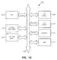
- FIG. 12is a block diagram of an electrical system, or processor-based system, utilizing oxide-conductor nanolaminates constructed in accordance with the present invention.
- wafer and substrate used in the following descriptioninclude any structure having an exposed surface with which to form the integrated circuit (IC) structure of the invention.
- substrateis understood to include semiconductor wafers.
- substrateis also used to refer to semiconductor structures during processing, and may include other layers that have been fabricated thereupon. Both wafer and substrate include doped and undoped semiconductors, epitaxial semiconductor layers supported by a base semiconductor or insulator, as well as other semiconductor structures well known to one skilled in the art.
- conductoris understood to include semiconductors
- insulatoris defined to include any material that is less electrically conductive than the materials referred to as conductors.
- FIG. 1Ais useful in illustrating the conventional operation of a MOSFET such as can be used in a DRAM array.
- FIG. 1Aillustrates the normal hot electron injection and degradation of devices operated in the forward direction. As is explained below, since the electrons are trapped near the drain they are not very effective in changing the device characteristics.
- FIG. 1Ais a block diagram of a metal oxide semiconductor field effect floating gate transistor (MOSFET) 101 in a substrate 100 .
- the MOSFET 101includes a source region 102 , a drain region 104 , a channel region 106 in the substrate 100 between the source region 102 and the drain region 104 .
- a gate 108is separated from the channel region 108 by a gate oxide 110 .
- a sourceline 112is coupled to the source region 102 .
- a bitline 114is coupled to the drain region 104 .
- a wordline 116is coupled to the gate 108 .
- a drain to source voltage potential(Vds) is set up between the drain region 104 and the source region 102 .
- a voltage potentialis then applied to the gate 108 via a wordline 116 .
- Vtcharacteristic voltage threshold
- a channel 106forms in the substrate 100 between the drain region 104 and the source region 102 . Formation of the channel 106 permits conduction between the drain region 104 and the source region 102 , and a current signal (Ids) can be detected at the drain region 104 .
- FIG. 1Cillustrates this point.
- FIG. 1Cis a graph showing the square root of the current signal (Ids) taken at the drain region versus the voltage potential (VGS) established between the gate 108 and the source region 102 .
- the change in the slope of the plot of ⁇ square root over (Ids) ⁇ versus VGSrepresents the change in the charge carrier mobility in the channel 106 .
- ⁇ VTrepresents the minimal change in the MOSFET's threshold voltage resulting from electrons gradually being trapped in the gate oxide 110 near the drain region 104 , under normal operation, due to device degradation. This results in a fixed trapped charge in the gate oxide 110 near the drain region 104 .
- Slope 103represents the charge carrier mobility in the channel 106 for FIG. 1A having no electrons trapped in the gate oxide 110 .
- Slope 105represents the charge mobility in the channel 106 for the conventional MOSFET of FIG. 1B having electrons 117 trapped in the gate oxide 110 near the drain region 104 .
- slope 103 and slope 105 in FIG. 1Cthe electrons 117 trapped in the gate oxide 110 near the drain region 104 of the conventional MOSFET do not significantly change the charge mobility in the channel 106 .
- One componentincludes a threshold voltage shift due to the trapped electrons and a second component includes mobility degradation due to additional scattering of carrier electrons caused by this trapped charge and additional surface states.
- a conventional MOSFETdegrades, or is “stressed,” over operation in the forward direction, electrons do gradually get injected and become trapped in the gate oxide near the drain. In this portion of the conventional MOSFET there is virtually no channel underneath the gate oxide. Thus the trapped charge modulates the threshold voltage and charge mobility only slightly.
- normal flash memory cellscan be programmed by operation in the reverse direction and utilizing avalanche hot electron injection to trap electrons on the floating gate of the floating gate transistor.
- the programmed floating gate transistorWhen the programmed floating gate transistor is subsequently operated in the forward direction the electrons trapped on the floating gate cause the channel to have a different threshold voltage.
- the novel programmed floating gate transistors of the present inventionconduct significantly less current than conventional flash cells which have not been programmed. These electrons will remain trapped on the floating gate unless negative control gate voltages are applied. The electrons will not be removed from the floating gate when positive or zero control gate voltages are applied. Erasure can be accomplished by applying negative control gate voltages and/or increasing the temperature with negative control gate bias applied to cause the trapped electrons on the floating gate to be re-emitted back into the silicon channel of the MOSFET.
- FIG. 2Ais a diagram of an embodiment for a programmed floating gate transistor cell 201 having oxide-conductor nanolaminate layers according to the teachings of the present invention.
- the floating gate transistor cell 201includes a floating gate transistor in a substrate 200 which has a first source/drain region 202 , a second source/drain region 204 , and a channel region 206 between the first and second source/drain regions, 202 and 204 .
- the first source/drain region 202includes a source region 202 for the floating gate transistor cell 201 and the second source/drain region 204 includes a drain region 204 for the floating gate transistor cell 201 .
- FIG. 1is a diagram of an embodiment for a programmed floating gate transistor cell 201 having oxide-conductor nanolaminate layers according to the teachings of the present invention.
- the floating gate transistor cell 201includes a floating gate transistor in a substrate 200 which has a first source/drain region 202 , a second source/drain region
- FIG. 2Afurther illustrates the floating gate transistor cell 201 having oxide-conductor nanolaminate layers 208 serving as a floating gate 208 and separated from the channel region 206 by a first gate oxide 210 .
- An sourceline or array plate 212is coupled to the first source/drain region 202 and a transmission line 214 is coupled to the second source/drain region 204 .
- the transmission line 214includes a bit line 214 .
- a control gate 216is separated from the oxide-conductor nanolaminate layers 208 , or floating gate 208 , by a second gate oxide 218 .
- floating gate transistor cell 201illustrates an embodiment of a programmed floating gate transistor.
- This programmed floating gate transistorhas a charge 217 trapped in potential wells in the oxide-conductor nanolaminate layers 208 , or floating gate 208 , formed by the different electron affinities between materials in the structures 208 , 210 and 218 .
- the charge 217 trapped on the floating gate 208includes a trapped electron charge 217 .
- FIG. 2Bis a diagram suitable for explaining the method by which the oxide-conductor nanolaminate layers 208 , or floating gate 208 , of the floating gate transistor cell 201 of the present invention can be programmed to achieve the embodiments of the present invention.
- the methodincludes programming the floating gate transistor.
- Programming the floating gate transistorincludes applying a first voltage potential V1 to a drain region 204 of the floating gate transistor and a second voltage potential V2 to the source region 202 .
- applying a first voltage potential V1 to the drain region 204 of the floating gate transistorincludes grounding the drain region 204 of the floating gate transistor as shown in FIG. 2B .
- applying a second voltage potential V2 to the source region 202includes biasing the array plate 212 to a voltage higher than VDD, as shown in FIG. 2B .
- a gate potential VGSis applied to the control gate 216 of the floating gate transistor.
- the gate potential VGSincludes a voltage potential which is less than the second voltage potential V2, but which is sufficient to establish conduction in the channel 206 of the floating gate transistor between the drain region 204 and the source region 202 . As shown in FIG.
- applying the first, second and gate potentials (V1, V2, and VGS respectively) to the floating gate transistorcreates a hot electron injection into the oxide-conductor nanolaminate layers 208 , or floating gate 208 , of the floating gate transistor.
- applying the first, second and gate potentials (V1, V2, and VGS respectively)provides enough energy to the charge carriers, e.g. electrons, being conducted across the channel 206 that, once the charge carriers are near the source region 202 , a number of the charge carriers get excited into the oxide-conductor nanolaminate layers 208 .
- the charge carriersbecome trapped in potential wells in the oxide-conductor nanolaminate layers 208 formed by the different electron affinities between materials in the structures 208 , 210 and 218 .
- applying a first voltage potential V1 to the drain region 204 of the floating gate transistorincludes biasing the drain region 204 of the floating gate transistor to a voltage higher than VDD.
- applying a second voltage potential V2 to the source region 202includes grounding the sourceline or array plate 212 .
- a gate potential VGSis applied to the control gate 216 of the floating gate transistor.
- the gate potential VGSincludes a voltage potential which is less than the first voltage potential V1, but which is sufficient to establish conduction in the channel 206 of the floating gate transistor between the drain region 204 and the source region 202 .
- Applying the first, second and gate potentials (V1, V2, and VGS respectively) to the floating gate transistorcreates a hot electron injection into the oxide-conductor nanolaminate layers 208 of the floating gate transistor.
- applying the first, second and gate potentials (V1, V2, and VGS respectively)provides enough energy to the charge carriers, e.g. electrons, being conducted across the channel 206 that, once the charge carriers are near the drain region 204 , a number of the charge carriers get excited into the oxide-conductor nanolaminate layers 208 , or floating gate 208 .
- the charge carriersbecome trapped in potential wells in the oxide-conductor nanolaminate layers 208 formed by the different electron affinities between materials in the structures 208 , 210 and 218 , as shown in FIG. 2A .
- the methodis continued by subsequently operating the floating gate transistor in the forward direction in its programmed state during a read operation.
- the read operationincludes grounding the source region 202 and precharging the drain region a fractional voltage of VDD. If the device is addressed by a wordline coupled to the gate, then its conductivity will be determined by the presence or absence of stored charge in the oxide-conductor nanolaminate layers 208 , or floating gate 208 . That is, a gate potential can be applied to the gate 216 by a wordline 220 in an effort to form a conduction channel between the source and the drain regions as done with addressing and reading conventional DRAM cells.
- the conduction channel 206 of the floating gate transistorwill have a higher voltage threshold and will not conduct.
- FIG. 2Cis a graph plotting a current signal (IDS) detected at the second source/drain region 204 versus a voltage potential, or drain voltage, (VDS) set up between the second source/drain region 204 and the first source/drain region 202 (IDS vs. VDS).
- VDSrepresents the voltage potential set up between the drain region 204 and the source region 202 .
- the curve plotted as 205represents the conduction behavior of a conventional floating gate transistor where the transistor is not programmed (is normal or not stressed) according to the teachings of the present invention.
- the curve 207represents the conduction behavior of the programmed floating gate transistor (stressed), described above in connection with FIG.
- the current signal (IDS 2 ) detected at the second source/drain region 204 for the programmed floating gate transistor (curve 207 )is significantly lower than the current signal (IDS 1 ) detected at the second source/drain region 204 for the conventional floating gate transistor cell (curve 205 ) which is not programmed according to the teachings of the present invention.
- VDSdrain voltage
- NROMflash memories
- This latter work in Israel and Germanyis based on employing charge trapping in a silicon nitride layer in a non-conventional flash memory device structure.
- Charge trapping in silicon nitride gate insulatorswas the basic mechanism used in MNOS memory devices
- charge trapping in aluminum oxide gateswas the mechanism used in MIOS memory devices
- one of the present inventors, along with another,has previously disclosed charge trapping at isolated point defects in gate insulators.
- none of the above described referencesaddressed forming transistor cells utilizing charge trapping in potential wells in oxide insulator nanolaminate layers formed by the different electron affinities of the insulators.
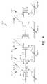
- FIG. 3illustrates an embodiment for a portion of a memory array 300 according to the teachings of the present invention.
- the memory in FIG. 3is shown illustrating a number of vertical pillars, or floating gate transistor cells, 301 - 1 , 301 - 2 , . . . , 301 -N, formed according to the teachings of the present invention.
- the number of vertical pillarare formed in rows and columns extending outwardly from a substrate 303 .
- the number of vertical pillars, 301 - 1 , 301 - 2 , . . . , 301 -Nare separated by a number of trenches 340 .
- the number of vertical pillars, 301 - 1 , 301 - 2 , . . . , 301 -Nserve as floating gate transistors including a first source/drain region, e.g. 302 - 1 and 302 - 2 respectively.
- the first source/drain region, 302 - 1 and 302 - 2is coupled to a sourceline 304 .
- the sourceline 304is formed in a bottom of the trenches 340 between rows of the vertical pillars, 301 - 1 , 301 - 2 , . . . , 301 -N.
- the sourceline 304is formed from a doped region implanted in the bottom of the trenches 340 .
- a second source/drain regione.g. 306 - 1 and 306 - 2 respectively, is coupled to a bitline (not shown).
- a channel region 305is located between the first and the second source/drain regions.
- oxide-conductor nanolaminate layers or floating gateare separated from the channel region 305 by a first oxide layer 307 in the trenches 340 along rows of the vertical pillars, 301 - 1 , 301 - 2 , . . . , 301 -N.
- a wordline 313is formed across the number of pillars and in the trenches 340 between the oxide-conductor nanolaminate layers 309 .
- the wordline 313is separated from the pillars and the oxide-conductor nanolaminate layers 309 , or floating gate 309 , by a second oxide layer 317 .
- the wordline 313serves as a control gate 313 for each pillar.
- FIG. 4illustrates an electrical equivalent circuit 400 for the portion of the memory array shown in FIG. 3 .
- a number of vertical floating gate transistor cells401 - 1 , 401 - 2 , . . . , 401 -N, are provided.
- a channel region 405 between the first and the second source/drain regionsa channel region 405 between the first and the second source/drain regions, and oxide-conductor nanolaminate layers serving as a floating gate, shown generally as 409 , separated from the channel region by a first oxide layer.
- FIG. 4further illustrates a number of bit lines, e.g. 411 - 1 and 411 - 2 .
- a single bit line, e.g. 411 - 1is coupled to the second source/drain regions, e.g. 406 - 1 and 406 - 2 , for a pair of floating gate transistor cells 401 - 1 and 401 - 2 since, as shown in FIG. 3 , each pillar contains two floating gate transistor cells.
- the number of bit lines, 411 - 1 and 411 - 2are coupled to the second source/drain regions, e.g.
- a number of word linessuch as wordline 413 in FIG. 4 , are coupled to a control gate 412 of each floating gate transistor cell along columns of the memory array.
- a number of sourcelines, 415 - 1 , 415 - 2 , . . . , 415 -Nare formed in a bottom of the trenches between rows of the vertical pillars, described in connection with FIG. 3 , such that first source/drain regions, e.g. 402 - 2 and 402 - 3 , in column adjacent floating gate transistor cells, e.g.
- 401 - 2 and 401 - 3separated by a trench, share a common sourceline, e.g. 415 - 1 .
- the number of sourcelines, 415 - 1 , 415 - 2 , . . . , 415 -Nare shared by column adjacent floating gate transistor cells, e.g. 401 - 2 and 401 - 3 , separated by a trench, along rows of the memory array 400 .
- column adjacent floating gate transistor cellse.g. 401 - 2 and 401 - 3 , separated by a trench, when one column adjacent floating gate transistor cell, e.g. 401 - 2 , is being read its complement column adjacent floating gate transistor cell, e.g. 401 - 3 , can operate as a reference cell.
- FIG. 5illustrates an energy band diagram for an embodiment of a gate stack according to the teachings of the present invention.
- the embodimentconsists of insulator stacks, 501 - 1 , oxide-conductor nanolaminate 501 - 2 and insulator stacks 501 - 3 , e.g. SiO 2 /oxide-conductor nanolaminate layers/SiO 2 .
- the structure shown in FIG. 5illustrates the present invention's use in various embodiments of metallic conductors, doped oxide conductors, and metals as a nanolaminate between two layers of silicon oxide.
- Tantalum nitride, titanium nitride, and tungsten nitrideare mid-gap work function metallic conductors described for use in CMOS devices. Tantalum nitride, titanium nitride, and tungsten nitride are employed in the present invention as oxide-conductor nanolaminate layers, formed by atomic layer deposition (ALD). These metallic conductors have large electron affinities around 4.7 eV which is larger than the 4.1 ev electron affinity of silicon oxide.
- atomic layer deposition, ALD, of a number of other conductorsis used to form the nanolaminate structures.
- ALDatomic layer deposition
- the oxide-conductor nanolaminate layers used in the present inventioninclude:
- Titanium nitride, tantalum nitride and tungsten nitrideare mid-gap work function metallic conductors, with no or zero band gaps and large electron affinities as shown in FIG. 6 , commonly described for use in CMOS devices.
- oxide-conductor nanolaminate layersas floating gates to trap charge in potential wells formed by the different electron affinities of the insulator layers.
- These layers formed by ALDare of atomic dimensions, or nanolaminates, with precisely controlled interfaces and layer thickness. Operation of the device specifically depends on and utilizes the electron affinity of the oxide-conductor nanolaminate layers being higher than that of silicon oxide. This creates a potential energy well in the multi-layer nanolaminate gate insulator structure.
- TaNPlasma-enhanced atomic layer deposition (PEALD) of tantalum nitride (Ta—N) thin films at a deposition temperature of 260° C. using hydrogen radicals as a reducing agent for Tertbutylimidotris(diethylamido)tantalum has been described.
- the PEALDyielded superior Ta—N films with an electric resistivity of 400 ⁇ cm and no aging effect under exposure to air.
- the film densityis higher than that of Ta—N films formed by typical ALD, in which NH 3 is used instead of hydrogen radicals.
- the as-deposited filmsare not amorphous, but rather polycrystalline structure of cubit TaN.
- the density and crystallinity of the filmsincreased with the pulse time of hydrogen plasma.
- the filmsare Ta-rich in composition and contain around 15 atomic % of carbon impurity.
- hydrogen radicalsare used a reducing agent instead of NH 3 , which is used as a reactant gas in typical Ta—N ALD.
- the liquid precursoris contained in a bubbler heated at 70° C. and carried by 35 sccm argon.
- One deposition cycleconsist of an exposure to a metallorganic precursor of TBTDET, a purge period with Ar, and an exposure to hydrogen plasma, followed by another purge period with Ar.
- the Ar purge periodof 15 seconds instead between each reactant gas pulse isolates the reactant gases from each other.
- a rectangular shaped electrical poweris applied between the upper and lower electrode.
- the showerhead for uniform distribution of the reactant gases in the reactorcapacitively coupled with an rf (13.56 MHz) plasma source operated at a power of 100 W, is used, as the upper electrode.
- the lower electrode, on which a wafer resides,is grounded. Film thickness and morphology are analyzed by field emission scanning electron microscopy.
- TiNAtomic layer deposition (ALD) of amorphous TiN films on SiO2 between 170° C. and 210° C. has been achieved by the alternate supply of reactant sources, Ti[N(C2H5CH3)2]4 [tetrakis(ethylmethylamino)titanium:TEMAT] and NH3.
- reactant sourcesTi[N(C2H5CH3)2]4 [tetrakis(ethylmethylamino)titanium:TEMAT] and NH3.
- reactant sourcesare injected into the reactor in the following order: TEMAT vapor pulse, Ar gas pulse, NH3 gas pulse and Ar gas pulse.
- Film thickness per cyclesaturated at around 1.6 monolayers per cycle with sufficient pulse times of reactant sources at 200° C. The results suggest that film thickness per cycle could exceed 1 ML/cycle in ALD, and are explained by the rechemisorption mechanism of the reactant sources. An ideal linear relationship between number of cycles and film thickness has been confirmed.
- TiN and TaNDeposition of thin and conformal copper films of has been examined using atomic layer deposition, ALD, of TiN and TaN as possible seed layer for subsequent electro-deposition.
- the copper filmsare deposited on glass as well as Ta, TIN, and TaN films on Si wafers. Typical resistivities of these films range from 4.25 ⁇ cm for 20 nm thick copper films to 1.78 ⁇ cm for 120 nm thick films.
- the adhesion of the copper films deposited on TiN and TaN at 300° C.is excellent. These films are highly conformal over high aspect ratio trenches.
- TiN, TaN x , NbN, and MoN xAtomic layer deposition of Tin, TaN x , NbN, and MoN x thin films from the corresponding metal chlorides and 1,1-dimethyl-hydrazine (DMHy) have been studied. Generally, the same films deposited at 400° C. exhibit better characteristics compared to the films deposited at the same temperature using NH 3 as the nitrogen source. In addition, films can be deposited at lower temperatures down to 200° C. Even though the carbon content in the films is quite high, in the range of 10 atom %, the results encourage further studies. The effect of carbon on the barrier properties and the use of other possibly less carbon-contaminating hydrazine derivatives can be considered.
- WNTungsten nitride films have been deposited with atomic layer control using sequential surface reactions. The tungsten nitride film growth is accomplished by separating the binary reaction 2WF 6 +NH 3 ⁇ >W 2 N+3HF+9/2 F2 into two half-reactions. Successive application of the WF 6 and NH 3 half-reactions in an ABAB . . . sequence produce tungsten nitride deposition at substrate temperatures between 600 and 800 K. Transmission Fourier transform infrared (FTIR) spectroscopy has been used to monitor the coverage Of WF x * and NH y * surface species on high surface area particles during the WF 6 and NH 3 half-reactions.
- FTIRTransmission Fourier transform infrared
- the FTIR spectroscope resultsdemonstrate the WF 6 and NH 3 half-reactions are complete and self-limiting at temperatures >600 K.
- In situ spectroscopic ellipsometryhas been used to monitor the film growth on Si( 100 ) substrate vs. temperature and reactant exposure.
- a tungsten nitride deposition rate of 2.55 ⁇ /AB cycleis measured at 600–800 K for WF 6 and NH 3 reactant exposure>3000 L and 10,000 L, respectively.
- X-ray photoelectron spectroscopy depth-profiling experimentshave been used to determine that the films had a W 2 N stoichiometry with low C and O impurity concentrations.
- X-ray diffraction investigationsreveal that the tungsten nitride films are microcrystalline. Atomic force microscopy measurements of the deposited films illustrate remarkably flat surface indicating smooth film growth. These smooth tungsten nitride films deposited with atomic layer have been be used as diffusion control for Cu on contact and via holes.
- ZnOcan be deposited by ALD.
- the aim of previous experimentsis to improve the performance of Cd-free ZnO/Cu(JnGa)Se 2 solar cells using a high-resistivity ZnO buffer layer.
- Buffer layersare deposited by atomic layer deposition (ALD) using diethylzinc (DEZn) and H 2 O as reactant gases.
- ALDatomic layer deposition
- DEZndiethylzinc
- H 2 Oreactant gases.
- the structural and electrical properties of the ZnO films on glass substrateshave been characterized.
- a high resistivity of more than 10 3 ⁇ cm and a transmittance of above 80% in the visible rangewere obtained.
- Suticai Chaitsak et al.focused on determining the optimum deposition parameters for the ALD-ZnO buffer layer.
- resultsindicate that the thickness and resistivity of the ALD-ZnO buffer layer, as well as the heat treatment prior to the deposition of the buffer layer, affect the device characteristics.
- the best efficiency obtained with an ALD-ZnO buffer layer of solar cells without an antireflective coatingis 12.1%.
- the reversible light soaking effectis observed in these devices.
- ZoO itself howeveris highly resistive, doping ZnO as described below is required to make it conductive and useful here.
- Films of ZnO 1 ⁇ x S xare deposited using dimethyzinc, 1% hydrogen sulfide in nitrogen, and the trace oxygen and/or water present (up to 2 ppm) in ultrahigh-purity (UHP) nitrogen.
- the dimethyzincis contained in a stainless steel cylinder equipped with a dip tube. To lower the dimethylzinc vapor pressure, the cylinder is held at 273 K using an ice water bath. Prepurified nitrogin served as a carrier gas for the dimethylzinc. Gas pressure are given in the table below:
- Nitrogen flush pressure50 psig Dimethylzinc cylinder pressure 50 psig Hydrogen sulfide cylinder pressure 30, 50, or 70 psig Dimethylzinc reaction time 2 s Hydrogen sulfide reaction time 5 s Nitrogen purge times 11 s at a standard flow rate of 1 L/mm Delay to allow nitrogen back- 0 8 s pressure to drop
- the electrical resistivity, mobility, and carrier concentration results from Hall measurements on some samplesare given in the following table:
- WThe atomic layer deposition (ALD) of tungsten (W) films has been demonstrated using alternate exposure of tungsten hexafluoride (WF 6 ) and disilane (Si 2 H 6 ).
- WF 6tungsten hexafluoride
- Si 2 H 6disilane
- the present investigationexplored the kinetics of the WF 6 and Si 2 H 6 surface reactions during W ALD at 303–623 K using Auger electron spectroscopy technique.
- the reaction of WF 6 with the Si 2 H 6 -saturated W surfaceproceeded to completion at 373–573 Kelvin (K).
- K373–573 Kelvin
- the WF 6 exposures necessary to reach saturationincreased with decreasing temperature.
- the WF 6 reactiondid not consume all the silicon (Si) surface species remaining from the previous Si 2 H 6 exposure.
- the reaction of Si 2 H 6 with the WF 6 -saturated W surfacedisplayed three kinetic regimes.
- the Si 2 H 6 reactionshowed an apparent saturation behavior with Si thickness at saturation at increased at substrate temperature.
- additional Siis deposited with an approximately logarithmic dependence on Si 2 H 6 exposure.
- a thin film of elementary nickelis formed by atomic layer deposition (ALD).
- the deposition cycleconsisted of two consecutive chemical reaction steps: an oxidizing step and a reducing step.
- An atomic layer of nickel oxideis made by sequentially supplying bis(cyclopentadienyl)-nickel as a nickel precursor and water as an oxidation agent; the preformed atomic layer of nickel oxide is then reduced to elementary nickel metal by exposure to hydrogen radical at a deposition temperature of 165° C.
- Auger electron spectroscopy analysisdetected negligible oxygen content in the grown films, indicating that the hydrogen radical had completely reduced the nickel oxide to metallic film films.
- carbon impurities in the filmdropped from 16 atomic % to less than 5 atomic % during the reaction.
- the proposed two-stage ALD method for elementary metalis successful in forming continuous and conformal nickel films.
- the nickel filmsformed an effective glue layer between chemical vapor deposited copper and diffusion barrier layer of TiN.
- the addition of a 1 ⁇ m thick copper film to a 15 nm thick nickel glue layer over a TiN barrier filmis excellent, with no failures occurring during adhesive tape peel tests.
- the gate insulator structure shown in FIG. 5is employed in a wide variety of different flash memory type devices. That is, in embodiments of the present invention, the gate structure embodiment of FIG. 5 , having silicon oxide-conductor-silicon oxide-nanolaminates, is used in place of the gate structure provided in the following commonly assigned patents: U.S. Pat. Nos. 5,936,274; 6,143,636; 5,973,356; 6,238,976; 5,991,225; 6,153,468; and 6,124,729.
- the gate structure embodiment of FIG. 5having silicon oxide-conductor silicon oxide-nanolaminates, is used in place of the gate structure provided in the following commonly assigned pending applications: Forbes, L., “Write Once Read Only Memory Employing Charge Trapping in Gate Insulators,” application Ser. No. 10/177,077; Forbes, L., “Write Once Read Only Memory Employing Floating Gates application Ser. No. 10/177,083; Forbes, L., “Write Once Read Only Memory With Large Work Function Floating Gates,” application Ser. No. 10/177,213; Forbes, L., “Nanocrystal Write Once Read Only Memory For Archival Storage,” application Ser. No.
- embodiments of the novel floating gate transistor hereinwhich are substituted for the gate structures described in the references above, are programmed by grounding a source line and applying a gate voltage and a voltage to the drain to cause channel hot electron injection.
- the drain and ground or sourcehave the normal connections and the conductivity of the floating gate transistor determined using low voltages so as not to disturb the memory state.
- the devicescan be erased by applying a large negative voltage to the gate.
- the gate structure embodiment of FIG. 5having silicon oxide-conductor-silicon oxide-nanolaminates, is used in place of the gate structure provided in the following commonly assigned patents: U.S. Pat. Nos. 5,936,274, 6,143,636, 5,973,356 and 6,238,976 (vertical flash memory devices with high density); U.S. Pat. Nos. 5,991,225 and 6,153,468 (programmable memory address and decode circuits); and U.S. Pat. No. 6,124,729 (programmable logic arrays).
- the gate structure embodiment of FIG. 5having silicon oxide-metal oxide-silicon oxide-conductor nanolaminates, is used in place of the gate structure provided in the following: Eitan, B. et al., “NROM: A novel localized Trapping, 2-Bit Nonvolatile Memory Cell,” IEEE Electron Device Lett., 21(11), 543–545 (November 2000); Eitan, B. et al., “Characterization of Channel Hot Electron Injection by the Subthreshold Slope of NROM device, IEEE Electron Device Lett., 22(11), 556–558 (November 2001); Maayan, E.
- the gate structure embodiment of FIG. 5having silicon oxide-metal oxide-silicon oxide-conductor nanolaminates used in place of the gate structures in those references, can be programmed in the reverse direction and read in the forward direction to obtain more sensitivity in the device characteristics to the stored charge.
- a floating gate transistor arrayincludes a number of floating gate transistor cells extending from a substrate, where the number of floating gate transistor cells operate as equivalent to a floating gate transistor having a size equal to or less than 2.0 lithographic feature squared (2F 2 ).
- an electronic systemincludes a number of floating gate transistors, where each floating gate transistor operates as equivalent to a floating transistor having a size equal to or less than 2.0 lithographic feature squared (2F 2 ).
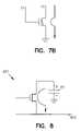
- FIGS. 7A–B and 8are embodiments useful in illustrating the use of charge storage in the oxide-conductor nanolaminate layers to modulate the conductivity of the floating gate transistor cell according to the teachings of the present invention. That is, FIGS. 7A–7B illustrates the operation of an embodiment for a novel floating gate transistor cell 701 formed according to the teachings of the present invention. And, FIG. 8 illustrates the operation of a conventional DRAM cell 701 . As shown in FIG. 7A , the embodiment consists of a gate insulator stack having insulator layers, 710 , 708 and 718 , e.g. SiO 2 /oxide-conductor nanolaminate layers/SiO 2 . In the embodiment of FIG.
- the gate insulator stack having insulator layers, 710 , 708 and 718has a thickness 711 thicker than in a conventional DRAM cell, e.g. 801 and is equal to or greater than 10 nm or 100 ⁇ (10 ⁇ 6 cm).
- a floating gate transistor cellhas dimensions 713 of 0.1 ⁇ m (10 ⁇ 5 cm) by 0.1 ⁇ m.
- the capacitance, Ci, of the structuredepends on the dielectric constant, ⁇ i , and the thickness of the insulating layers, t.
- a charge of 10 12 electrons/cm 2is programmed into the oxide-conductor nanolaminate layers of the floating gate transistor cell.
- the charge carriersbecome trapped in potential wells in the oxide-conductor nanolaminate layers 708 formed by the different electron affinities of the insulators 710 , 708 and 718 , as shown in FIG. 7A .
- This produces a stored charge ⁇ Q10 12 electrons/cm 2 ⁇ 1.6 ⁇ 10 ⁇ 19 Coulombs.
- an original V Tis approximately 1 ⁇ 2 Volt and the V T with charge trapping is approximately 1 Volt.
- FIG. 7Baids to further illustrate the conduction behavior of the novel floating gate transistor cell of the present invention.
- Vthe nominal threshold voltage without the floating gate charged
- the oxide-conductor nanolaminate layersare charged the floating gate transistor cell of the present invention will be off and not conduct.
- an un-written, or un-programmed floating gate transistor cellcan conduct a current of the order 12.5 ⁇ A, whereas if the oxide-conductor nanolaminate layers are charged then the floating gate transistor cell will not conduct.
- the sense amplifiers used in DRAM arrayscan easily detect such differences in current on the bit lines.
- the floating gate transistor cellshaving the gate structure with oxide-conductor nanolaminate layers, in the array are utilized not just as passive on or off switches as transfer devices in DRAM arrays but rather as active devices providing gain.
- to program the floating gate transistor cell “off,”requires only a stored charge in the oxide-conductor nanolaminate layers of about 100 electrons if the area is 0.1 ⁇ m by 0.1 ⁇ m.
- the floating gate transistor cellis un-programmed, e.g. no stored charge trapped in the oxide-conductor nanolaminate layers, and if the floating gate transistor cell is addressed over 10 nS a current of 12.5 ⁇ A is provided.
- the integrated drain currentthen has a charge of 125 fC or 800,000 electrons. This is in comparison to the charge on a DRAM capacitor of 50 fC which is only about 300,000 electrons.
- the use of floating gate transistor cells, having the gate structure with oxide-conductor nanolaminate layers, in the array as active devices with gain, rather than just switches,provides an amplification of the stored charge, in the oxide-conductor nanolaminate layers, from 100 to 800,000 electrons over a read address period of 10 nS.
- the memory device 940contains a memory array 942 , row and column decoders 944 , 948 and a sense amplifier circuit 946 .
- the memory array 942consists of a plurality of floating gate transistor cells 900 , having oxide-conductor nanolaminate layers in the gate stack, whose word lines 980 and bit lines 960 are commonly arranged into rows and columns, respectively.
- the bit lines 960 of the memory array 942are connected to the sense amplifier circuit 946 , while its word lines 980 are connected to the row decoder 944 .
- Address and control signalsare input on address/control lines 961 into the memory device 940 and connected to the column decoder 948 , sense amplifier circuit 946 and row decoder 944 and are used to gain read and write access, among other things, to the memory array 942 .
- the column decoder 948is connected to the sense amplifier circuit 946 via control and column select signals on column select lines 962 .
- the sense amplifier circuit 946receives input data destined for the memory array 942 and outputs data read from the memory array 942 over input/output (I/O) data lines 963 .
- Datais read from the cells of the memory array 942 by activating a word line 980 (via the row decoder 944 ), which couples all of the memory cells corresponding to that word line to respective bit lines 960 , which define the columns of the array.
- One or more bit lines 960are also activated.
- the sense amplifier circuit 946 connected to a bit line columndetects and amplifies the conduction sensed through a given floating gate transistor cell and transferred to its bit line 960 by measuring the potential difference between the activated bit line 960 and a reference line which may be an inactive bit line. Again, in the read operation the source region of a given cell is couple to a grounded sourceline or array plate (not shown).
- the operation of Memory device sense amplifiersis described, for example, in U.S. Pat. Nos. 5,627,785; 5,280,205; and 5,042,011, all assigned to Micron Technology Inc., and incorporated by reference herein.
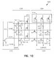
- FIG. 10shows a conventional NOR-NOR logic array 1000 which is programmable at the gate mask level by either fabricating a thin oxide gate transistor, e.g. logic cells 1001 - 1 , 1001 - 2 , . . . , 1001 -N and 1003 - 1 , 1003 - 2 , . . . , 1003 -N, at the intersection of lines in the array or not fabricating a thin oxide gate transistor, e.g. missing thin oxide transistors, 1002 - 1 , 1002 - 2 , . . . , 1002 -N, at such an intersection.
- a thin oxide gate transistore.g. logic cells 1001 - 1 , 1001 - 2 , . . . , 1001 -N and 1003 - 1 , 1003 - 2 , . . . , 1003 -N, at such an intersection.
- NMOS transistors1016 and 1018 respectively, are used as load devices.
- the conventional logic array shown in FIG. 10includes a first logic plane 1010 which receives a number of input signals at input lines 1012 .
- first logic plane 1010can include inverters to produce the complementary signals when needed in a specific application.
- First logic plane 1010includes a number of thin oxide gate transistors, e.g. transistors 1001 - 1 , 1001 - 2 , . . . , 1001 -N.
- the thin oxide gate transistors, 1001 - 1 , 1001 - 2 , . . . , 1001 -N,are located at the intersection of input lines 1012 , and interconnect lines 1014 .
- this selective fabrication of thin oxide gate transistore.g. transistors 1001 - 1 , 1001 - 2 , . . .
- 1001 -Nis referred to as programming since the logical function implemented by the programmable logic array is entered into the array by the selective arrangement of the thin oxide gate transistors, or logic cells, 1001 - 1 , 1001 - 2 , . . . , 1001 -N, at the intersections of input lines 1012 , and interconnect lines 1014 in the array.
- each of the interconnect lines 1014acts as a NOR gate for the input lines 1012 that are connected to the interconnect lines 1014 through the thin oxide gate transistors, 1001 - 1 , 1001 - 2 , . . . , 1001 -N, of the array.
- interconnection line 1014 Aacts as a NOR gate for the signals on input lines 1012 A and 1012 B. That is, interconnect line 1014 A is maintained at a high potential unless one or more of the thin oxide gate transistors, 1001 - 1 , 1001 - 2 , . . . , 1001 -N, that are coupled to interconnect line 1014 A are turned on by a high logic level signal on one of the input lines 1012 .
- each thin oxide gate transistore.g. transistors 1001 - 1 , 1001 - 2 , . . . , 1001 -N, conducts which performs the NOR positive logic circuit function
- an inversion of the OR circuit functionresults from inversion of data onto the interconnect lines 1014 through the thin oxide gate transistors, 1001 - 1 , 1001 - 2 , . . . , 1001 -N, of the array.
- a second logic plane 1024which includes a number of thin oxide gate transistor, e.g. transistors 1003 - 1 , 1003 - 2 , . . . , 1003 -N.
- the thin oxide gate transistors, 1003 - 1 , 1003 - 2 , . . . , 1003 -N,are located at the intersection of interconnect lines 1014 , and output lines 1020 .
- the logical function of the second logic plane 1024is implemented by the selective arrangement of the thin oxide gate transistors, 1003 - 1 , 1003 - 2 , . . .
- the second logic plane 1024is also configured such that the output lines 1020 comprise a logical NOR function of the signals from the interconnection lines 1014 that are coupled to particular output lines 1020 through the thin oxide gate transistors, 1003 - 1 , 1003 - 2 , . . . , 1003 -N, of the second logic plane 1024 .
- the incoming signals on each lineare used to drive the gates of transistors in the NOR logic array as the same is known by one of ordinary skill in the art and will be understood by reading this disclosure.
- FIG. 11illustrates an embodiment of a novel in-service programmable logic array (PLA) formed with logic cells having a floating gate structure with oxide-conductor nanolaminate layers, according to the teachings of the present invention.
- PLA 1100implements an illustrative logical function using a two level logic approach.
- PLA 1100includes first and second logic planes 1110 and 1122 .
- the logic functionis implemented using NOR-NOR logic.
- first and second logic planes 1110 and 1122each include an array of, logic cells, having a gate structure with oxide-conductor nanolaminate layers, which serve as driver floating gate transistors, 1101 - 1 , 1101 - 2 , . .
- driver floating gate transistors1101 - 1 , 1101 - 2 , . . . , 1101 -N, and 1102 - 1 , 1102 - 2 , . . . , 1102 -N respectively, formed according to the teachings of the present invention.
- the driver floating gate transistors, 1101 - 1 , 1101 - 2 , . . . , 1101 -N, and 1102 - 1 , 1102 - 2 , . . . , 1102 -Nhave their first source/drain regions coupled to source lines or a conductive source plane.
- the driver floating gate transistors, 1101 - 1 , 1101 - 2 , . . . , 1101 -N, and 1102 - 1 , 1102 - 2 , . . . , 1102 -Nare shown as n-channel floating gate transistors. However, the invention is not so limited. Also, as shown in FIG. 11 , a number of p-channel metal oxide semiconductor (PMOS) floating gate transistors are provided as load device floating gate transistors, 1116 and 1124 respectively, having their source regions coupled to a voltage potential (VDD).
- PMOSmetal oxide semiconductor
- load device floating gate transistors, 1116 and 1124respectively, operate in complement to the driver floating gate transistors, 1101 - 1 , 1101 - 2 , . . . , 1101 -N, and 1102 - 1 , 1102 - 2 , . . . , 1102 -N to form load inverters.
- FIG. 11is provided by way of example and not by way of limitation. Specifically, the teachings of the present application are not limited to programmable logic arrays in the NOR-NOR approach. Further, the teachings of the present application are not limited to the specific logical function shown in FIG. 11 . Other logical functions can be implemented in a programmable logic array, with the driver floating gate transistors, having a gate structure with oxide-conductor nanolaminate layers, 1101 - 1 , 1101 - 2 , . . . , 1101 -N, and 1102 - 1 , 1102 - 2 , . . . , 1102 -N and load device floating gate transistors, 1116 and 1124 respectively, of the present invention, using any one of the various two level logic approaches.
- First logic plane 1110receives a number of input signals at input lines 1112 .
- no invertersare provided for generating complements of the input signals.
- first logic plane 1110can include inverters to produce the complementary signals when needed in a specific application.
- First logic plane 1110includes a number of driver floating gate transistors, having a gate structure with oxide-conductor nanolaminate layers, 1101 - 1 , 1101 - 2 , . . . , 1101 -N, that form an array.
- the driver floating gate transistors, 1101 - 1 , 1101 - 2 , . . . , 1101 -Nare located at the intersection of input lines 1112 , and interconnect lines 1114 . Not all of the driver floating gate transistors, 1101 - 1 , 1101 - 2 , . . . , 1101 -N, are operatively conductive in the first logic plane.
- the driver floating gate transistors, 1101 - 1 , 1101 - 2 , . . . , 1101 -Nare selectively programmed, as has been described herein, to respond to the input lines 1112 and change the potential of the interconnect lines 1114 so as to implement a desired logic function.
- This selective interconnectionis referred to as programming since the logical function implemented by the programmable logic array is entered into the array by the driver floating gate transistors, 1101 - 1 , 1101 - 2 , . . . , 1101 -N, that are used at the intersections of input lines 1112 , and interconnect lines 1114 in the array.
- each of the interconnect lines 1114acts as a NOR gate for the input lines 1112 that are connected to the interconnect lines 1114 through the driver floating gate transistors, 1101 - 1 , 1101 - 2 , . . . , 1101 -N, of the array 1100 .
- interconnection line 1114 Aacts as a NOR gate for the signals on input lines 1112 A, 1112 B and 1112 C.
- Programmability of the driver floating gate transistors, 1101 - 1 , 1101 - 2 , . . . , 1101 -Nis achieved by trapping charge carriers in potential wells in the oxide-conductor nanolaminate layers of the gate stack, as described herein.
- That driver floating gate transistor, 1101 - 1 , 1101 - 2 , . . . , 1101 -Nwill remain in an off state until it is reprogrammed.
- Applying and removing a charge to the oxide-conductor nanolaminate layersis performed by tunneling charge into the oxide-conductor nanolaminate layers of the driver floating gate transistors, 1101 - 1 , 1101 - 2 , . . . , 1101 -N.
- a driver floating gate transistors, 1101 - 1 , 1101 - 2 , . . . , 1101 -N programmed in an off stateremains in that state until the charge is removed from the oxide-conductor nanolaminate layers.
- Driver floating gate transistors, 1101 - 1 , 1101 - 2 , . . . , 1101 -N not having their corresponding gate structure with oxide-conductor nanolaminate layers chargedoperate in either an on state or an off state, wherein input signals received by the input lines 1112 A, 1112 B and 1112 C determine the applicable state. If any of the input lines 1112 A, 1112 B and 1112 C are turned on by input signals received by the input lines 1112 A, 1112 B and 1112 C, then a ground is provided to load device floating gate transistors 1116 . The load device floating gate transistors 1116 are attached to the interconnect lines 1114 .
- the load device floating gate transistors 1116provide a low voltage level when any one of the driver floating gate transistors, 1101 - 1 , 1101 - 2 , . . . , 1101 -N connected to the corresponding interconnect line 1114 is activated. This performs the NOR logic circuit function, an inversion of the OR circuit function results from inversion of data onto the interconnect lines 1114 through the driver floating gate transistors, 1101 - 1 , 1101 - 2 , . . . , 1101 -N of the array 1100 .
- each of the driver floating gate transistors, 1101 - 1 , 1101 - 2 , . . . , 1101 -N described hereinare formed according to the teachings of the present, having a gate structure with oxide-conductor nanolaminate layers.
- second logic plane 1122comprises a second array of driver floating gate transistors, 1102 - 1 , 1102 - 2 , . . . , 1102 -N that are selectively programmed to provide the second level of the two level logic needed to implement a specific logical function.
- the array of driver floating gate transistors, 1102 - 1 , 1102 - 2 , . . . , 1102 -Nis also configured such that the output lines 1120 comprise a logical NOR function of the signals from the interconnection lines 1114 that are coupled to particular output lines 1120 through the driver floating gate transistors, 1102 - 1 , 1102 - 2 , . . . , 1102 -N of the second logic plane 1122 .
- Applying and removing a charge to the oxide-conductor nanolaminate layersare performed by tunneling charge into the oxide-conductor nanolaminate layers of the driver floating gate transistors, 1101 - 1 , 1101 - 2 , . . . , 1101 -N.
- a driver floating gate transistor, e.g. 1102 - 1 , 1102 - 2 , . . . , 1102 -N, programmed in an off stateremains in that state until the charge is removed from the oxide-conductor nanolaminate layers.
- Driver floating gate transistors, 1102 - 1 , 1102 - 2 , . . . , 1102 -N not having their corresponding gate structure with oxide-conductor nanolaminate layers chargedoperate in either an on state or an off state, wherein signals received by the interconnect lines 1114 determine the applicable state. If any of the interconnect lines 1114 are turned on, then a ground is provided to load device floating gate transistors 1124 by applying a ground potential to the source line or conductive source plane coupled to the floating gate transistors first source/drain region as described herein. The load device floating gate transistors 1124 are attached to the output lines 1120 .
- the load device floating gate transistors 1124provide a low voltage level when any one of the driver floating gate transistors, 1102 - 1 , 1102 - 2 , . . . , 1102 -N connected to the corresponding output line is activated. This performs the NOR logic circuit function, an inversion of the OR circuit function results from inversion of data onto the output lines 1120 through the driver floating gate transistors, 1102 - 1 , 1102 - 2 , . . . , 1102 -N of the array 1100 .
- each of the driver floating gate transistors, 1102 - 1 , 1102 - 2 , . . . , 1102 -N described hereinare formed according to the teachings of the present, having a gate structure with oxide-conductor nanolaminate layers.
- FIG. 11shows an embodiment for the application of the novel floating gate transistor cells, having a gate structure with oxide-conductor nanolaminate layers, in a logic array.
- a driver floating gate transistors1101 - 1 , 1101 - 2 , . . . , 1101 -N, and 1102 - 1 , 1102 - 2 , . . . , 1102 -N, is programmed with a negative charge trapped in potential wells, formed with the oxide-conductor nanolaminate layers, it is effectively removed from the array.
- the array logic functionscan be programmed even when the circuit is in the final circuit or in the field and being used in a system.
- the absence or presence of charge trapped in potential wells, formed by the oxide-conductor nanolaminate layers,is read by addressing the input lines 1112 or control gate lines and y-column/sourcelines to form a coincidence in address at a particular logic cell.
- the control gate linewould for instance be driven positive at some voltage of 1.0 Volts and the y-column/sourceline grounded, if the oxide-conductor nanolaminate layers are not charged with electrons then the floating gate transistor would turn on tending to hold the interconnect line on that particular row down indicating the presence of a stored “one” in the cell.
- this particular floating gate transistor cellhas charge trapped in potential wells, formed by the oxide-conductor nanolaminate layers, the floating gate transistor will not turn on and the presence of a stored “zero” is indicated in the cell. In this manner, data stored on a particular floating gate transistor cell can be read.
- Programmingcan be achieved by hot electron injection.
- the interconnect lines, coupled to the second source/drain region for the floating gate transistor cells in the first logic plane,are driven with a higher drain voltage like 2 Volts for 0.1 micron technology and the control gate line is addressed by some nominal voltage in the range of twice this value. Erasure is accomplished by driving the control gate line with a large positive voltage and the sourceline and/or backgate or substrate/well address line of the floating gate transistor with a negative bias so the total voltage difference is in the order of 3 Volts causing electrons to tunnel out of the oxide-conductor nanolaminate layers of the driver floating gate transistors.
- Writingcan be performed, as also described above, by normal channel hot electron injection
- FIG. 12is a block diagram of an electrical system, or processor-based system, 1200 utilizing floating gate transistor cells with a gate structure having oxide-conductor nanolaminate layers.
- memory 1212is constructed in accordance with the present invention to have floating gate transistor cells with a gate structure having oxide-conductor nanolaminate layers. The same applies to floating gate transistors in the CPU, etc., the invention is not so limited.
- the processor-based system 1200may be a computer system, a process control system or any other system employing a processor and associated memory.
- the system 1200includes a central processing unit (CPU) 1202 , e.g., a microprocessor, that communicates with the NOR flash memory 1212 and an I/O device 1208 over a bus 1220 .
- CPUcentral processing unit
- the bus 1220may be a series of buses and bridges commonly used in a processor-based system, but for convenience purposes only, the bus 1220 has been illustrated as a single bus.
- a second I/O device 1210is illustrated, but is not necessary to practice the invention.
- the processor-based system 1200can also includes read-only memory (ROM) 1214 and may include peripheral devices such as a floppy disk drive 1204 and a compact disk (CD) ROM drive 1206 that also communicates with the CPU 1202 over the bus 1220 as is well known in the art.
- ROMread-only memory
- peripheral devicessuch as a floppy disk drive 1204 and a compact disk (CD) ROM drive 1206 that also communicates with the CPU 1202 over the bus 1220 as is well known in the art.
- CDcompact disk
- At least one of the floating gate transistor cells, having a gate structure with oxide-conductor nanolaminate layers in memory 1212includes a programmed floating gate transistor cell according to the teachings of the present invention.
- FIG. 12illustrates an embodiment for electronic system circuitry in which the novel floating gate transistor cells of the present invention are used.
- the illustration of system 1200is intended to provide a general understanding of one application for the structure and circuitry of the present invention, and is not intended to serve as a complete description of all the elements and features of an electronic system using the novel floating gate transistor cell structures.
- the inventionis equally applicable to any size and type of memory device 1200 using the novel floating gate transistor cells of the present invention and is not intended to be limited to that described above.
- such an electronic systemcan be fabricated in single-package processing units, or even on a single semiconductor chip, in order to reduce the communication time between the processor and the memory device.
- Applications containing the novel floating gate transistor cell of the present invention as described in this disclosureinclude electronic systems for use in memory modules, device drivers, power modules, communication modems, processor modules, and application-specific modules, and may include multilayer, multichip modules.
- Such circuitrycan further be a subcomponent of a variety of electronic systems, such as a clock, a television, a cell phone, a personal computer, an automobile, an industrial control system, an aircraft, and others.
- This disclosuredescribes the use of oxide-conductor nanolaminate layers as floating gates to trap charge in potential wells formed by the different electron affinities of the oxide-conductor nanolaminate layers. That is, this disclosure describes a flash memory device, programmable logic array device or memory address and decode correction device with a conductor nanolaminate floating gate rather than a conventional polysilicon floating gate.
Landscapes
- Engineering & Computer Science (AREA)
- Computer Hardware Design (AREA)
- Non-Volatile Memory (AREA)
- Semiconductor Memories (AREA)
Abstract
Description
- Boulin et al., “Semiconductor Memory Apparatus with a Multi-Layer Insulator Contacting the Semiconductor,” U.S. Pat. No. 3,877,054;
- Kahng et al., “Method for Fabricating Multilayer Insulator-Semiconductor Memory Apparatus,” U.S. Pat. No. 3,964,085;
- DiMaria, D. J., “Graded or Stepped Energy Band-Gap-Insulator MIS structures (GI-MIS or SI-MIS),” Journal of Applied Physics, 50(9). 5826–9 (September 1979);
- DeKeersmaecker et al., “Non-Volatile Memory Devices Fabricated From Graded or Stepped Energy Band Gap Insulator MIM or MIS Structure,” U.S. Pat. No. 4,217,601, RE31,083;
- Eitan, “Non-volatile semiconductor memory cell utilizing asymmetrical charge trapping,” U.S. Pat. No. 5,768,192;
- Etian, B. et al., “NROM: A Novel Localized Trapping, 2-Bit Nonvolatile Memory Cell,” IEEE Electron Device Lett., 21(11), 543–545 (November 2000);
- Eitan, B. et al., “Characterization of Channel Hot Electron Injection by the Subthreshold Slope of NROM device, IEEE Electron Device Lett., 22(11), 556–558 (November 2001);
- Frohman-Bentchkowsky, D., “An Integrated Metal-Nitride-Oxide-Silicon (MNOS) Memory,” Proceedings of the IEEE, 57(6), 1190–2 (June 1969);
- Nakamuma et al., “Memory matrix using MIS semiconductor element,” U.S. Pat. No. 3,665,423;
- Britton, J. et al., “Metal-Nitride-Oxide IC Memory Retains Data for Meter Reader,” Electronics, 45(22); 119–23 (23 Oct. 1972);
- B. Dipert and L. Hebert, “Flash Memory goes Mainstream,” IEEE Spectrum, No. 10, pp. 48–52, (October 1993);
- R. Goodwins, “New Memory Technologies on the Way,” http://zdnet.com.com/2100-1103-846950.html);
- C. -G. Hwang, “Semiconductor Memories for the IT Era,” Abst. IEEE Int. Solid-State Circuits Conf., San Francisco, 2002, pp. 24–27;
- R. Shirota et al., “A 2.3 mu2memory cell structure for 16 Mb NAND EEPROMs,” Digest of IEEE Int. Electron Device Meeting, San Francisco, 1990, pp. 103–106;
- L. Forbes, W. P. Noble and E. H. Cloud, “MOSFET Technology for Programmable Address Decode and Correction,” U.S. Pat. No. 6,521,950;
- S. Sze, Physics of Semiconductor Devices, Wiley, N.Y., 1981, pp. 504–506);
- L. Forbes and J. Geusic, “Memory Using Insulator Traps,” U.S. Pat. No. 6,140,181;
- A. Yagishita et al., “Dynamic threshold voltage damascene metal gate MOSFET (DT-DMG-MOS) with low threshold voltage, high drive current and uniform electrical characteristics,” Digest Technical Papers Int. Electron Devices Meeting, San Francisco, pp. 663–666 (December 2000);
- H. Shimada et al., “Tantalum Nitride Metal Gate FD-SOI CMOS FETs Using Low Resistivity Self-Grown BCC-Tantalum Layer,” IEEE Trans. Electron Devices, Vol. 48, No. 8, pp. 1619–1626 (2000);
- M. Moriwaki et al. “Improved Metal Gate Process by Simultaneous Gate-Oxide Nitridation During W/WN/Sub X/Gate Formation,” Jpn. J. Appl. Phys., Vol. 39, No. 4B, pp. 2177–2180 (2000);
- A. Yagishita et al., “Dynamic Threshold Voltage Damascene Metal Gate MOSFET (DT-DMG-MOS) With Low Threshold Voltage, High Drive Current and Uniform Electrical Characteristics,” Digest Technical Papers Int. Electron Devices Meeting, San Francisco, December 2000, pp. 663–666;
- Jin-Seong Park et al, “Plasma-Enhanced Atomic Layer Deposition of Tantalum Nitrides Using Hydrogen Radicals as a Reducing Agent,” Electrochemical and Solid-State Lett.);
- J. -S. Min et al., “Atomic Layer Deposition of TiN Films by Alternate Supply on Tetrakis (Ethylmethyllamino)-Titanium and Ammonia,” Jpn. J. Appl. Phys., Vol. 37,
Part 1, No. 9A, pp. 4999–5004 (15 Sep. 1998); - Raj Solanki et al., “Atomic Layer Deposition of Copper Seed Layers,” Electrochemical and Solid-State Letters, 3 (10) 479–480 (2000);
- Marika Juppo et al., “Use of 1,1-Dimethylhydrazine in the Atomic Layer Deposition of Transition Metal Nitride Thin Films,” Jour. of the Electrochemical Soc., 147 (9) 3377–3381 (2000);
- Kraus, J. W. et al., “Atomic Layer Deposition of Tungsten Nitride Films Using Sequential Surface Reactions,” Jour. of the Electrochemical Soc., Vol. 147, No. 3, 1173–1181 (2000);
- Suticai Chaitsak et al, “Cu(InGa)Se2Thin-Film Solar Cells with High Resistivity ZnO Buffer Layers Deposited by Atomic Layer Deposition,” Jpn. J. Appl. Phys., Vol. 38, pp. 4989–4992 (1999);
- B. W. Sanders et al, “Zinc Oxysulfide Thin Films Grown by Atomic Layer Deposition,” Chem. Mater. 1992, 4, 1005–1011;
- Elam, J. W. et al., “Kinetics of the WF6and Si2H6Surface Reactions During Tungsten Atomic Layer Deposition,” Surface Science, Vol. 479, No. 1–3, pp. 121–135 (2001);
- Junghun Chea et al., “Atomic Layer Deposition of Nickel by the Reduction of Preformed Nickel Oxide,” Electrochemical and Solid-State Letters, 5, (6) C4–C66 (2002);
- Forbes et al., “High Density Flash Memory,” U.S. Pat. Nos. 5,936,274, 6,143,636;
- Noble et al., “Ultra High Density Flash Memory,” U.S. Pat. No. 5,973,356;
- Noble et al., “Method of Forming High Density Flash Memory,” U.S. Pat. No. 6,238,976;
- Forbes et al., “Programmable Memory Address Decode Array with Vertical Transistors,” U.S. Pat. No. 5,991,225;
- Forbes et al., “Method of Forming a Logic Array for a Decoder,” U.S. Pat. No. 6,153,468;
- Nobel et al., “Field Programmable Logic Arrays with Vertical Transistors,” U.S. Pat. No. 6,124,729;
- (i) Metallic Conductors, TaN, TiN, WN, NbN, MoN
- (ii) Doped Oxide Conductors, ZnOS
- (iii) Metals, including tungsten, W, and Nickel, Ni
| Nitrogen flush pressure | 50 psig |
| Dimethylzinc cylinder pressure | 50 psig |
| Hydrogen sulfide cylinder pressure | 30, 50, or 70 psig |
| Dimethylzinc reaction time | 2 s |
| Hydrogen sulfide reaction time | 5 s |
| Nitrogen purge times | 11 s at a standard flow rate of |
| 1 L/mm | |
| Delay to allow nitrogen back- | 0 8 s |
| pressure to drop | |
The electrical resistivity, mobility, and carrier concentration results from Hall measurements on some samples are given in the following table:
| X in | Resistivity, | Donor concentration, | Mobility, |
| ZnO1−xSx | Ω cm | cm−3 | cm2/V s |
| 0 | 0.0048 | 4.8 × 10¹⁹ | 13.2 |
| 0.25 | 0.101 | 1.7 × 10¹⁸ | 36.1 |
| 0.56 | 0.042 | 1.66 × 10¹⁹ | 32.2 |
| 0.66 | 1.28 | 2.0 × 10¹⁷ | 24 |
| 0.82 | 8.27 | 2.4 × 10¹⁶ | 28 |
| 0.92 | 67.9 | 2.61 × 10¹⁵ | 94 |
Atomic Layer Deposition of Metal Films
Claims (30)
Priority Applications (4)
| Application Number | Priority Date | Filing Date | Title |
|---|---|---|---|
| US10/191,336US7221017B2 (en) | 2002-07-08 | 2002-07-08 | Memory utilizing oxide-conductor nanolaminates |
| US11/217,767US20070178643A1 (en) | 2002-07-08 | 2005-08-31 | Memory utilizing oxide-conductor nanolaminates |
| US11/217,771US7583534B2 (en) | 2002-07-08 | 2005-08-31 | Memory utilizing oxide-conductor nanolaminates |
| US11/496,196US7687848B2 (en) | 2002-07-08 | 2006-07-31 | Memory utilizing oxide-conductor nanolaminates |
Applications Claiming Priority (1)
| Application Number | Priority Date | Filing Date | Title |
|---|---|---|---|
| US10/191,336US7221017B2 (en) | 2002-07-08 | 2002-07-08 | Memory utilizing oxide-conductor nanolaminates |
Related Child Applications (3)
| Application Number | Title | Priority Date | Filing Date |
|---|---|---|---|
| US11/217,767DivisionUS20070178643A1 (en) | 2002-07-08 | 2005-08-31 | Memory utilizing oxide-conductor nanolaminates |
| US11/217,771DivisionUS7583534B2 (en) | 2002-07-08 | 2005-08-31 | Memory utilizing oxide-conductor nanolaminates |
| US11/496,196DivisionUS7687848B2 (en) | 2002-07-08 | 2006-07-31 | Memory utilizing oxide-conductor nanolaminates |
Publications (2)
| Publication Number | Publication Date |
|---|---|
| US20040004245A1 US20040004245A1 (en) | 2004-01-08 |
| US7221017B2true US7221017B2 (en) | 2007-05-22 |
Family
ID=29999976
Family Applications (4)
| Application Number | Title | Priority Date | Filing Date |
|---|---|---|---|
| US10/191,336Expired - Fee RelatedUS7221017B2 (en) | 2002-07-08 | 2002-07-08 | Memory utilizing oxide-conductor nanolaminates |
| US11/217,771Expired - LifetimeUS7583534B2 (en) | 2002-07-08 | 2005-08-31 | Memory utilizing oxide-conductor nanolaminates |
| US11/217,767AbandonedUS20070178643A1 (en) | 2002-07-08 | 2005-08-31 | Memory utilizing oxide-conductor nanolaminates |
| US11/496,196Expired - LifetimeUS7687848B2 (en) | 2002-07-08 | 2006-07-31 | Memory utilizing oxide-conductor nanolaminates |
Family Applications After (3)
| Application Number | Title | Priority Date | Filing Date |
|---|---|---|---|
| US11/217,771Expired - LifetimeUS7583534B2 (en) | 2002-07-08 | 2005-08-31 | Memory utilizing oxide-conductor nanolaminates |
| US11/217,767AbandonedUS20070178643A1 (en) | 2002-07-08 | 2005-08-31 | Memory utilizing oxide-conductor nanolaminates |
| US11/496,196Expired - LifetimeUS7687848B2 (en) | 2002-07-08 | 2006-07-31 | Memory utilizing oxide-conductor nanolaminates |
Country Status (1)
| Country | Link |
|---|---|
| US (4) | US7221017B2 (en) |
Cited By (25)
| Publication number | Priority date | Publication date | Assignee | Title |
|---|---|---|---|---|
| US20040004247A1 (en)* | 2002-07-08 | 2004-01-08 | Micron Technology, Inc. | Memory utilizing oxide-nitride nanolaminates |
| US20060008966A1 (en)* | 2002-07-08 | 2006-01-12 | Micron Technology, Inc. | Memory utilizing oxide-conductor nanolaminates |
| US20060240626A1 (en)* | 2002-06-21 | 2006-10-26 | Micron Technology, Inc. | Write once read only memory employing charge trapping in insulators |
| US20060284246A1 (en)* | 2002-07-08 | 2006-12-21 | Micron Technology, Inc. | Memory utilizing oxide nanolaminates |
| US20080032475A1 (en)* | 2006-08-02 | 2008-02-07 | Spansion Llc | Memory cell system with gradient charge isolation |
| US7405454B2 (en) | 2003-03-04 | 2008-07-29 | Micron Technology, Inc. | Electronic apparatus with deposited dielectric layers |
| US7410910B2 (en) | 2005-08-31 | 2008-08-12 | Micron Technology, Inc. | Lanthanum aluminum oxynitride dielectric films |
| US7554161B2 (en) | 2002-06-05 | 2009-06-30 | Micron Technology, Inc. | HfAlO3 films for gate dielectrics |
| US20090174010A1 (en)* | 2008-01-03 | 2009-07-09 | International Business Machines Corporation | Sram device structure including same band gap transistors having gate stacks with high-k dielectrics and same work function |
| US7560395B2 (en) | 2005-01-05 | 2009-07-14 | Micron Technology, Inc. | Atomic layer deposited hafnium tantalum oxide dielectrics |
| US7572695B2 (en) | 2005-05-27 | 2009-08-11 | Micron Technology, Inc. | Hafnium titanium oxide films |
| US7575978B2 (en) | 2005-08-04 | 2009-08-18 | Micron Technology, Inc. | Method for making conductive nanoparticle charge storage element |
| US7588988B2 (en) | 2004-08-31 | 2009-09-15 | Micron Technology, Inc. | Method of forming apparatus having oxide films formed using atomic layer deposition |
| US7589029B2 (en) | 2002-05-02 | 2009-09-15 | Micron Technology, Inc. | Atomic layer deposition and conversion |
| US20090290416A1 (en)* | 2008-05-22 | 2009-11-26 | Kabushiki Kaisha Toshiba | Nonvolatile semiconductor memory device |
| US7625794B2 (en) | 2003-03-31 | 2009-12-01 | Micron Technology, Inc. | Methods of forming zirconium aluminum oxide |
| US7670646B2 (en) | 2002-05-02 | 2010-03-02 | Micron Technology, Inc. | Methods for atomic-layer deposition |
| US7709402B2 (en) | 2006-02-16 | 2010-05-04 | Micron Technology, Inc. | Conductive layers for hafnium silicon oxynitride films |
| US7719065B2 (en) | 2004-08-26 | 2010-05-18 | Micron Technology, Inc. | Ruthenium layer for a dielectric layer containing a lanthanide oxide |
| US7754618B2 (en) | 2005-02-10 | 2010-07-13 | Micron Technology, Inc. | Method of forming an apparatus having a dielectric containing cerium oxide and aluminum oxide |
| US20100197095A1 (en)* | 2009-02-03 | 2010-08-05 | John Mark Meldrim | Methods Of Forming Memory Cells |
| US7867919B2 (en) | 2004-08-31 | 2011-01-11 | Micron Technology, Inc. | Method of fabricating an apparatus having a lanthanum-metal oxide dielectric layer |
| US7927948B2 (en) | 2005-07-20 | 2011-04-19 | Micron Technology, Inc. | Devices with nanocrystals and methods of formation |
| US7989290B2 (en) | 2005-08-04 | 2011-08-02 | Micron Technology, Inc. | Methods for forming rhodium-based charge traps and apparatus including rhodium-based charge traps |
| US8110469B2 (en) | 2005-08-30 | 2012-02-07 | Micron Technology, Inc. | Graded dielectric layers |
Families Citing this family (59)
| Publication number | Priority date | Publication date | Assignee | Title |
|---|---|---|---|---|
| US6521958B1 (en)* | 1999-08-26 | 2003-02-18 | Micron Technology, Inc. | MOSFET technology for programmable address decode and correction |
| US6674667B2 (en)* | 2001-02-13 | 2004-01-06 | Micron Technology, Inc. | Programmable fuse and antifuse and method therefor |
| US6852167B2 (en) | 2001-03-01 | 2005-02-08 | Micron Technology, Inc. | Methods, systems, and apparatus for uniform chemical-vapor depositions |
| US7253467B2 (en) | 2001-06-28 | 2007-08-07 | Samsung Electronics Co., Ltd. | Non-volatile semiconductor memory devices |
| US8253183B2 (en) | 2001-06-28 | 2012-08-28 | Samsung Electronics Co., Ltd. | Charge trapping nonvolatile memory devices with a high-K blocking insulation layer |
| US20060180851A1 (en)* | 2001-06-28 | 2006-08-17 | Samsung Electronics Co., Ltd. | Non-volatile memory devices and methods of operating the same |
| US7012297B2 (en)* | 2001-08-30 | 2006-03-14 | Micron Technology, Inc. | Scalable flash/NV structures and devices with extended endurance |
| US7068544B2 (en)* | 2001-08-30 | 2006-06-27 | Micron Technology, Inc. | Flash memory with low tunnel barrier interpoly insulators |
| US7075829B2 (en)* | 2001-08-30 | 2006-07-11 | Micron Technology, Inc. | Programmable memory address and decode circuits with low tunnel barrier interpoly insulators |
| US6784480B2 (en)* | 2002-02-12 | 2004-08-31 | Micron Technology, Inc. | Asymmetric band-gap engineered nonvolatile memory device |
| US7045430B2 (en)* | 2002-05-02 | 2006-05-16 | Micron Technology Inc. | Atomic layer-deposited LaAlO3 films for gate dielectrics |
| US7205218B2 (en) | 2002-06-05 | 2007-04-17 | Micron Technology, Inc. | Method including forming gate dielectrics having multiple lanthanide oxide layers |
| US7193893B2 (en)* | 2002-06-21 | 2007-03-20 | Micron Technology, Inc. | Write once read only memory employing floating gates |
| US6996009B2 (en) | 2002-06-21 | 2006-02-07 | Micron Technology, Inc. | NOR flash memory cell with high storage density |
| US7154140B2 (en)* | 2002-06-21 | 2006-12-26 | Micron Technology, Inc. | Write once read only memory with large work function floating gates |
| US6921702B2 (en)* | 2002-07-30 | 2005-07-26 | Micron Technology Inc. | Atomic layer deposited nanolaminates of HfO2/ZrO2 films as gate dielectrics |
| US7084078B2 (en)* | 2002-08-29 | 2006-08-01 | Micron Technology, Inc. | Atomic layer deposited lanthanide doped TiOx dielectric films |
| US7101813B2 (en)* | 2002-12-04 | 2006-09-05 | Micron Technology Inc. | Atomic layer deposited Zr-Sn-Ti-O films |
| US6958302B2 (en)* | 2002-12-04 | 2005-10-25 | Micron Technology, Inc. | Atomic layer deposited Zr-Sn-Ti-O films using TiI4 |
| US7183186B2 (en)* | 2003-04-22 | 2007-02-27 | Micro Technology, Inc. | Atomic layer deposited ZrTiO4 films |
| SE0301350D0 (en)* | 2003-05-08 | 2003-05-08 | Forskarpatent I Uppsala Ab | A thin-film solar cell |
| US7192824B2 (en)* | 2003-06-24 | 2007-03-20 | Micron Technology, Inc. | Lanthanide oxide / hafnium oxide dielectric layers |
| US7220665B2 (en)* | 2003-08-05 | 2007-05-22 | Micron Technology, Inc. | H2 plasma treatment |
| TW200514256A (en)* | 2003-10-15 | 2005-04-16 | Powerchip Semiconductor Corp | Non-volatile memory device and method of manufacturing the same |
| US7184315B2 (en)* | 2003-11-04 | 2007-02-27 | Micron Technology, Inc. | NROM flash memory with self-aligned structural charge separation |
| US8197468B2 (en)* | 2003-11-13 | 2012-06-12 | Synergetics, Inc. | Surgical instrument handle with adjustable actuator position |
| US7301804B2 (en)* | 2003-12-16 | 2007-11-27 | Micro Technology, Inc. | NROM memory cell, memory array, related devices and methods |
| US7050330B2 (en)* | 2003-12-16 | 2006-05-23 | Micron Technology, Inc. | Multi-state NROM device |
| WO2005093837A1 (en)* | 2004-03-29 | 2005-10-06 | Industry-University Cooperation Foundation Hanyang University | Flash memory device utilizing nanocrystals embeded in polymer |
| US7601649B2 (en)* | 2004-08-02 | 2009-10-13 | Micron Technology, Inc. | Zirconium-doped tantalum oxide films |
| US8501828B2 (en)* | 2004-08-11 | 2013-08-06 | Huntsman Petrochemical Llc | Cure rebond binder |
| US20060113586A1 (en)* | 2004-11-29 | 2006-06-01 | Macronix International Co., Ltd. | Charge trapping dielectric structure for non-volatile memory |
| US7235501B2 (en) | 2004-12-13 | 2007-06-26 | Micron Technology, Inc. | Lanthanum hafnium oxide dielectrics |
| KR100576081B1 (en)* | 2005-01-31 | 2006-05-03 | 삼성전자주식회사 | Thin film manufacturing method, flash memory device manufacturing method and capacitor manufacturing method using same |
| KR100631905B1 (en)* | 2005-02-22 | 2006-10-11 | 삼성전기주식회사 | Nitride single crystal substrate manufacturing method and nitride semiconductor light emitting device manufacturing method using the same |
| US7687409B2 (en) | 2005-03-29 | 2010-03-30 | Micron Technology, Inc. | Atomic layer deposited titanium silicon oxide films |
| US8314024B2 (en) | 2008-12-19 | 2012-11-20 | Unity Semiconductor Corporation | Device fabrication |
| US7662729B2 (en)* | 2005-04-28 | 2010-02-16 | Micron Technology, Inc. | Atomic layer deposition of a ruthenium layer to a lanthanide oxide dielectric layer |
| US7679118B2 (en) | 2005-06-13 | 2010-03-16 | Micron Technology, Inc. | Vertical transistor, memory cell, device, system and method of forming same |
| US20070049023A1 (en)* | 2005-08-29 | 2007-03-01 | Micron Technology, Inc. | Zirconium-doped gadolinium oxide films |
| US8071476B2 (en) | 2005-08-31 | 2011-12-06 | Micron Technology, Inc. | Cobalt titanium oxide dielectric films |
| US7615446B2 (en) | 2005-10-13 | 2009-11-10 | Samsung Electronics Co., Ltd. | Charge trap flash memory device, fabrication method thereof, and write/read operation control method thereof |
| KR100719047B1 (en) | 2005-12-19 | 2007-05-16 | 한양대학교 산학협력단 | A multilevel flash memory device using a multi-layered nanoparticle layer formed spontaneously in a polymer thin film as a floating gate, a fabrication method thereof, and a method of controlling the write / read operation thereof |
| US7605030B2 (en) | 2006-08-31 | 2009-10-20 | Micron Technology, Inc. | Hafnium tantalum oxynitride high-k dielectric and metal gates |
| KR101146589B1 (en)* | 2006-11-30 | 2012-05-16 | 삼성전자주식회사 | Charge trap semiconductor memory device and manufacturing method the same |
| CN101207179B (en)* | 2006-12-19 | 2012-05-23 | 国际商业机器公司 | Memory cell and its manufacturing method |
| US20080272421A1 (en)* | 2007-05-02 | 2008-11-06 | Micron Technology, Inc. | Methods, constructions, and devices including tantalum oxide layers |
| US8012532B2 (en) | 2007-12-18 | 2011-09-06 | Micron Technology, Inc. | Methods of making crystalline tantalum pentoxide |
| US7973357B2 (en)* | 2007-12-20 | 2011-07-05 | Samsung Electronics Co., Ltd. | Non-volatile memory devices |
| US8208241B2 (en)* | 2008-06-04 | 2012-06-26 | Micron Technology, Inc. | Crystallographically orientated tantalum pentoxide and methods of making same |
| US8759876B2 (en)* | 2008-10-06 | 2014-06-24 | Massachusetts Institute Of Technology | Enhancement-mode nitride transistor |
| US8891283B2 (en)* | 2009-01-05 | 2014-11-18 | Hewlett-Packard Development Company, L.P. | Memristive device based on current modulation by trapped charges |
| CN102044289B (en)* | 2009-10-20 | 2012-12-05 | 中芯国际集成电路制造(上海)有限公司 | Green transistor, nano silicon ferroelectric memory and driving method thereof |
| US8892808B2 (en)* | 2011-04-22 | 2014-11-18 | Hewlett-Packard Development Company, L.P. | Retention-value associated memory |
| KR102442621B1 (en) | 2015-11-30 | 2022-09-13 | 삼성전자주식회사 | Methods of forming thin film and integrated circuit device using niobium compound |
| JP6717024B2 (en)* | 2016-04-18 | 2020-07-01 | 富士通株式会社 | MEMORY AND MEMORY CONTROL METHOD |
| US9859157B1 (en) | 2016-07-14 | 2018-01-02 | International Business Machines Corporation | Method for forming improved liner layer and semiconductor device including the same |
| CN115020229A (en)* | 2022-05-30 | 2022-09-06 | 上海华力集成电路制造有限公司 | A process method for improving continuity of metal floating gate |
| US12428727B2 (en)* | 2022-06-13 | 2025-09-30 | Tokyo Electron Limited | Cyclic film deposition using reductant gas |
Citations (125)
| Publication number | Priority date | Publication date | Assignee | Title |
|---|---|---|---|---|
| US3665423A (en) | 1969-03-15 | 1972-05-23 | Nippon Electric Co | Memory matrix using mis semiconductor element |
| US3877054A (en) | 1973-03-01 | 1975-04-08 | Bell Telephone Labor Inc | Semiconductor memory apparatus with a multilayer insulator contacting the semiconductor |
| US3964085A (en) | 1975-08-18 | 1976-06-15 | Bell Telephone Laboratories, Incorporated | Method for fabricating multilayer insulator-semiconductor memory apparatus |
| US4217601A (en) | 1979-02-15 | 1980-08-12 | International Business Machines Corporation | Non-volatile memory devices fabricated from graded or stepped energy band gap insulator MIM or MIS structure |
| US4413022A (en) | 1979-02-28 | 1983-11-01 | Canon Kabushiki Kaisha | Method for performing growth of compound thin films |
| US4507673A (en) | 1979-10-13 | 1985-03-26 | Tokyo Shibaura Denki Kabushiki Kaisha | Semiconductor memory device |
| US4661833A (en) | 1984-10-30 | 1987-04-28 | Kabushiki Kaisha Toshiba | Electrically erasable and programmable read only memory |
| US4939559A (en) | 1981-12-14 | 1990-07-03 | International Business Machines Corporation | Dual electron injector structures using a conductive oxide between injectors |
| US5021999A (en) | 1987-12-17 | 1991-06-04 | Mitsubishi Denki Kabushiki Kaisha | Non-volatile semiconductor memory device with facility of storing tri-level data |
| US5027171A (en) | 1989-08-28 | 1991-06-25 | The United States Of America As Represented By The Secretary Of The Navy | Dual polarity floating gate MOS analog memory device |
| JPH03222367A (en) | 1990-01-26 | 1991-10-01 | Fujitsu Ltd | Insulated gate type field effect transistor |
| US5111430A (en) | 1989-06-22 | 1992-05-05 | Nippon Telegraph And Telephone Corporation | Non-volatile memory with hot carriers transmitted to floating gate through control gate |
| US5253196A (en) | 1991-01-09 | 1993-10-12 | The United States Of America As Represented By The Secretary Of The Navy | MOS analog memory with injection capacitors |
| US5274249A (en) | 1991-12-20 | 1993-12-28 | University Of Maryland | Superconducting field effect devices with thin channel layer |
| US5293560A (en) | 1988-06-08 | 1994-03-08 | Eliyahou Harari | Multi-state flash EEPROM system using incremental programing and erasing methods |
| US5298447A (en) | 1993-07-22 | 1994-03-29 | United Microelectronics Corporation | Method of fabricating a flash memory cell |
| US5303182A (en) | 1991-11-08 | 1994-04-12 | Rohm Co., Ltd. | Nonvolatile semiconductor memory utilizing a ferroelectric film |
| US5317535A (en) | 1992-06-19 | 1994-05-31 | Intel Corporation | Gate/source disturb protection for sixteen-bit flash EEPROM memory arrays |
| JPH06224431A (en) | 1993-01-26 | 1994-08-12 | Sharp Corp | Thin-film transistor and liquid crystal display panel |
| JPH06302828A (en) | 1993-04-14 | 1994-10-28 | Matsushita Electric Ind Co Ltd | Nonvolatile semiconductor memory device |
| US5388069A (en) | 1992-03-19 | 1995-02-07 | Fujitsu Limited | Nonvolatile semiconductor memory device for preventing erroneous operation caused by over-erase phenomenon |
| US5409859A (en) | 1992-09-10 | 1995-04-25 | Cree Research, Inc. | Method of forming platinum ohmic contact to p-type silicon carbide |
| US5424993A (en) | 1993-11-15 | 1995-06-13 | Micron Technology, Inc. | Programming method for the selective healing of over-erased cells on a flash erasable programmable read-only memory device |
| US5430670A (en) | 1993-11-08 | 1995-07-04 | Elantec, Inc. | Differential analog memory cell and method for adjusting same |
| US5434815A (en) | 1994-01-19 | 1995-07-18 | Atmel Corporation | Stress reduction for non-volatile memory cell |
| US5438544A (en) | 1993-03-19 | 1995-08-01 | Fujitsu Limited | Non-volatile semiconductor memory device with function of bringing memory cell transistors to overerased state, and method of writing data in the device |
| US5449941A (en) | 1991-10-29 | 1995-09-12 | Semiconductor Energy Laboratory Co., Ltd. | Semiconductor memory device |
| US5467306A (en) | 1993-10-04 | 1995-11-14 | Texas Instruments Incorporated | Method of using source bias to increase threshold voltages and/or to correct for over-erasure of flash eproms |
| US5477485A (en) | 1995-02-22 | 1995-12-19 | National Semiconductor Corporation | Method for programming a single EPROM or FLASH memory cell to store multiple levels of data that utilizes a floating substrate |
| US5485422A (en) | 1994-06-02 | 1996-01-16 | Intel Corporation | Drain bias multiplexing for multiple bit flash cell |
| US5493140A (en) | 1993-07-05 | 1996-02-20 | Sharp Kabushiki Kaisha | Nonvolatile memory cell and method of producing the same |
| US5508543A (en)* | 1994-04-29 | 1996-04-16 | International Business Machines Corporation | Low voltage memory |
| US5530581A (en) | 1995-05-31 | 1996-06-25 | Eic Laboratories, Inc. | Protective overlayer material and electro-optical coating using same |
| JPH08255878A (en) | 1995-03-16 | 1996-10-01 | Fujitsu Ltd | Floating gate transistor and manufacturing method thereof |
| US5602777A (en) | 1994-09-28 | 1997-02-11 | Sharp Kabushiki Kaisha | Semiconductor memory device having floating gate transistors and data holding means |
| US5627781A (en) | 1994-11-11 | 1997-05-06 | Sony Corporation | Nonvolatile semiconductor memory |
| US5670790A (en) | 1995-09-21 | 1997-09-23 | Kabushikik Kaisha Toshiba | Electronic device |
| US5698022A (en) | 1996-08-14 | 1997-12-16 | Advanced Technology Materials, Inc. | Lanthanide/phosphorus precursor compositions for MOCVD of lanthanide/phosphorus oxide films |
| US5714766A (en) | 1995-09-29 | 1998-02-03 | International Business Machines Corporation | Nano-structure memory device |
| US5740104A (en) | 1997-01-29 | 1998-04-14 | Micron Technology, Inc. | Multi-state flash memory cell and method for programming single electron differences |
| US5754477A (en) | 1997-01-29 | 1998-05-19 | Micron Technology, Inc. | Differential flash memory cell and method for programming |
| US5768192A (en) | 1996-07-23 | 1998-06-16 | Saifun Semiconductors, Ltd. | Non-volatile semiconductor memory cell utilizing asymmetrical charge trapping |
| US5795808A (en) | 1995-11-13 | 1998-08-18 | Hyundai Electronics Industries C., Ltd. | Method for forming shallow junction for semiconductor device |
| US5801401A (en) | 1997-01-29 | 1998-09-01 | Micron Technology, Inc. | Flash memory with microcrystalline silicon carbide film floating gate |
| US5828605A (en) | 1997-10-14 | 1998-10-27 | Taiwan Semiconductor Manufacturing Company Ltd. | Snapback reduces the electron and hole trapping in the tunneling oxide of flash EEPROM |
| US5840897A (en) | 1990-07-06 | 1998-11-24 | Advanced Technology Materials, Inc. | Metal complex source reagents for chemical vapor deposition |
| US5852306A (en) | 1997-01-29 | 1998-12-22 | Micron Technology, Inc. | Flash memory with nanocrystalline silicon film floating gate |
| US5856688A (en) | 1997-05-09 | 1999-01-05 | Samsung Electronics Co., Ltd. | Integrated circuit memory devices having nonvolatile single transistor unit cells therein |
| WO1999007000A2 (en) | 1997-08-01 | 1999-02-11 | Saifun Semiconductors Ltd. | Two bit eeprom using asymmetrical charge trapping |
| US5886368A (en) | 1997-07-29 | 1999-03-23 | Micron Technology, Inc. | Transistor with silicon oxycarbide gate and methods of fabrication and use |
| WO1999017371A1 (en) | 1997-09-26 | 1999-04-08 | Thunderbird Technologies, Inc. | Metal gate fermi-threshold field effect transistors |
| US5912488A (en) | 1996-07-30 | 1999-06-15 | Samsung Electronics Co., Ltd | Stacked-gate flash EEPROM memory devices having mid-channel injection characteristics for high speed programming |
| US5936274A (en) | 1997-07-08 | 1999-08-10 | Micron Technology, Inc. | High density flash memory |
| US5943262A (en) | 1997-12-31 | 1999-08-24 | Samsung Electronics Co., Ltd. | Non-volatile memory device and method for operating and fabricating the same |
| US5973356A (en) | 1997-07-08 | 1999-10-26 | Micron Technology, Inc. | Ultra high density flash memory |
| US5991225A (en) | 1998-02-27 | 1999-11-23 | Micron Technology, Inc. | Programmable memory address decode array with vertical transistors |
| US6005790A (en) | 1998-12-22 | 1999-12-21 | Stmicroelectronics, Inc. | Floating gate content addressable memory |
| US6020024A (en) | 1997-08-04 | 2000-02-01 | Motorola, Inc. | Method for forming high dielectric constant metal oxides |
| US6027961A (en) | 1998-06-30 | 2000-02-22 | Motorola, Inc. | CMOS semiconductor devices and method of formation |
| US6049479A (en) | 1999-09-23 | 2000-04-11 | Advanced Micro Devices, Inc. | Operational approach for the suppression of bi-directional tunnel oxide stress of a flash cell |
| US6072209A (en) | 1997-07-08 | 2000-06-06 | Micro Technology, Inc. | Four F2 folded bit line DRAM cell structure having buried bit and word lines |
| US6110529A (en) | 1990-07-06 | 2000-08-29 | Advanced Tech Materials | Method of forming metal films on a substrate by chemical vapor deposition |
| US6115281A (en) | 1997-06-09 | 2000-09-05 | Telcordia Technologies, Inc. | Methods and structures to cure the effects of hydrogen annealing on ferroelectric capacitors |
| US6122201A (en) | 1999-10-20 | 2000-09-19 | Taiwan Semiconductor Manufacturing Company | Clipped sine wave channel erase method to reduce oxide trapping charge generation rate of flash EEPROM |
| US6124729A (en) | 1998-02-27 | 2000-09-26 | Micron Technology, Inc. | Field programmable logic arrays with vertical transistors |
| US6160739A (en) | 1999-04-16 | 2000-12-12 | Sandisk Corporation | Non-volatile memories with improved endurance and extended lifetime |
| US6171900B1 (en) | 1999-04-15 | 2001-01-09 | Taiwan Semiconductor Manufacturing Company | CVD Ta2O5/oxynitride stacked gate insulator with TiN gate electrode for sub-quarter micron MOSFET |
| US6194228B1 (en) | 1997-10-22 | 2001-02-27 | Fujitsu Limited | Electronic device having perovskite-type oxide film, production thereof, and ferroelectric capacitor |
| US6203613B1 (en) | 1999-10-19 | 2001-03-20 | International Business Machines Corporation | Atomic layer deposition with nitrate containing precursors |
| US6212103B1 (en)* | 1999-07-28 | 2001-04-03 | Xilinx, Inc. | Method for operating flash memory |
| US6222768B1 (en) | 2000-01-28 | 2001-04-24 | Advanced Micro Devices, Inc. | Auto adjusting window placement scheme for an NROM virtual ground array |
| US6225168B1 (en) | 1998-06-04 | 2001-05-01 | Advanced Micro Devices, Inc. | Semiconductor device having metal gate electrode and titanium or tantalum nitride gate dielectric barrier layer and process of fabrication thereof |
| US6232643B1 (en) | 1997-11-13 | 2001-05-15 | Micron Technology, Inc. | Memory using insulator traps |
| US6243300B1 (en) | 2000-02-16 | 2001-06-05 | Advanced Micro Devices, Inc. | Substrate hole injection for neutralizing spillover charge generated during programming of a non-volatile memory cell |
| US6294813B1 (en) | 1998-05-29 | 2001-09-25 | Micron Technology, Inc. | Information handling system having improved floating gate tunneling devices |
| US6310376B1 (en) | 1997-10-03 | 2001-10-30 | Sharp Kabushiki Kaisha | Semiconductor storage device capable of improving controllability of density and size of floating gate |
| US6313518B1 (en) | 1997-10-14 | 2001-11-06 | Micron Technology, Inc. | Porous silicon oxycarbide integrated circuit insulator |
| US6320786B1 (en) | 2000-12-22 | 2001-11-20 | Macronix International Co., Ltd. | Method of controlling multi-state NROM |
| US6320784B1 (en) | 2000-03-14 | 2001-11-20 | Motorola, Inc. | Memory cell and method for programming thereof |
| US20020003252A1 (en)* | 1998-09-03 | 2002-01-10 | Ravi Iyer | Flash memory circuit with with resistance to disturb effect |
| US6353554B1 (en) | 1995-02-27 | 2002-03-05 | Btg International Inc. | Memory apparatus including programmable non-volatile multi-bit memory cell, and apparatus and method for demarcating memory states of the cell |
| US20020027264A1 (en) | 1999-08-26 | 2002-03-07 | Micron Technology, Inc. | MOSFET technology for programmable address decode and correction |
| US6365470B1 (en) | 2000-08-24 | 2002-04-02 | Secretary Of Agency Of Industrial Science And Technology | Method for manufacturing self-matching transistor |
| US6387712B1 (en) | 1996-06-26 | 2002-05-14 | Tdk Corporation | Process for preparing ferroelectric thin films |
| US20020074565A1 (en) | 2000-06-29 | 2002-06-20 | Flagan Richard C. | Aerosol silicon nanoparticles for use in semiconductor device fabrication |
| US20020089023A1 (en) | 2001-01-05 | 2002-07-11 | Motorola, Inc. | Low leakage current metal oxide-nitrides and method of fabricating same |
| US6420902B1 (en)* | 2000-05-31 | 2002-07-16 | Micron Technology, Inc. | Field programmable logic arrays with transistors with vertical gates |
| US6429063B1 (en) | 1999-10-26 | 2002-08-06 | Saifun Semiconductors Ltd. | NROM cell with generally decoupled primary and secondary injection |
| US6432779B1 (en) | 2000-05-18 | 2002-08-13 | Motorola, Inc. | Selective removal of a metal oxide dielectric |
| US20020115252A1 (en) | 2000-10-10 | 2002-08-22 | Haukka Suvi P. | Dielectric interface films and methods therefor |
| US6445030B1 (en) | 2001-01-30 | 2002-09-03 | Advanced Micro Devices, Inc. | Flash memory erase speed by fluorine implant or fluorination |
| US6445023B1 (en) | 1999-03-16 | 2002-09-03 | Micron Technology, Inc. | Mixed metal nitride and boride barrier layers |
| US6449188B1 (en) | 2001-06-19 | 2002-09-10 | Advanced Micro Devices, Inc. | Low column leakage nor flash array-double cell implementation |
| US6456536B1 (en) | 2000-06-23 | 2002-09-24 | Advanced Micro Devices, Inc. | Method of programming a non-volatile memory cell using a substrate bias |
| US6456531B1 (en) | 2000-06-23 | 2002-09-24 | Advanced Micro Devices, Inc. | Method of drain avalanche programming of a non-volatile memory cell |
| US6458701B1 (en) | 1999-10-20 | 2002-10-01 | Samsung Electronics Co., Ltd. | Method for forming metal layer of semiconductor device using metal halide gas |
| US6459618B1 (en) | 2000-08-25 | 2002-10-01 | Advanced Micro Devices, Inc. | Method of programming a non-volatile memory cell using a drain bias |
| US6465306B1 (en) | 2000-11-28 | 2002-10-15 | Advanced Micro Devices, Inc. | Simultaneous formation of charge storage and bitline to wordline isolation |
| US6487121B1 (en) | 2000-08-25 | 2002-11-26 | Advanced Micro Devices, Inc. | Method of programming a non-volatile memory cell using a vertical electric field |
| US6490204B2 (en) | 2000-05-04 | 2002-12-03 | Saifun Semiconductors Ltd. | Programming and erasing methods for a reference cell of an NROM array |
| US6490205B1 (en) | 2000-02-16 | 2002-12-03 | Advanced Micro Devices, Inc. | Method of erasing a non-volatile memory cell using a substrate bias |
| US6504755B1 (en)* | 1999-05-14 | 2003-01-07 | Hitachi, Ltd. | Semiconductor memory device |
| US20030032270A1 (en) | 2001-08-10 | 2003-02-13 | John Snyder | Fabrication method for a device for regulating flow of electric current with high dielectric constant gate insulating layer and source/drain forming schottky contact or schottky-like region with substrate |
| US6521950B1 (en) | 1993-06-30 | 2003-02-18 | The United States Of America As Represented By The Secretary Of The Navy | Ultra-high resolution liquid crystal display on silicon-on-sapphire |
| US6552387B1 (en) | 1997-07-30 | 2003-04-22 | Saifun Semiconductors Ltd. | Non-volatile electrically erasable and programmable semiconductor memory cell utilizing asymmetrical charge trapping |
| US6559014B1 (en) | 2001-10-15 | 2003-05-06 | Advanced Micro Devices, Inc. | Preparation of composite high-K / standard-K dielectrics for semiconductor devices |
| US6567312B1 (en) | 2000-05-15 | 2003-05-20 | Fujitsu Limited | Non-volatile semiconductor memory device having a charge storing insulation film and data holding method therefor |
| US6567303B1 (en) | 2001-01-31 | 2003-05-20 | Advanced Micro Devices, Inc. | Charge injection |
| US6570787B1 (en) | 2002-04-19 | 2003-05-27 | Advanced Micro Devices, Inc. | Programming with floating source for low power, low leakage and high density flash memory devices |
| US6580118B2 (en) | 1999-06-08 | 2003-06-17 | Infineon Technologies Ag | Non-volatile semiconductor memory cell having a metal oxide dielectric, and method for fabricating the memory cell |
| US6580124B1 (en)* | 2000-08-14 | 2003-06-17 | Matrix Semiconductor Inc. | Multigate semiconductor device with vertical channel current and method of fabrication |
| US6618290B1 (en) | 2000-06-23 | 2003-09-09 | Advanced Micro Devices, Inc. | Method of programming a non-volatile memory cell using a baking process |
| US6642573B1 (en) | 2002-03-13 | 2003-11-04 | Advanced Micro Devices, Inc. | Use of high-K dielectric material in modified ONO structure for semiconductor devices |
| US20030235077A1 (en) | 2002-06-21 | 2003-12-25 | Micron Technology, Inc. | Write once read only memory employing floating gates |
| US20030235066A1 (en) | 2002-06-21 | 2003-12-25 | Micron Technology, Inc. | Ferroelectric write once read only memory for archival storage |
| US20030235081A1 (en) | 2002-06-21 | 2003-12-25 | Micron Technology, Inc. | Nanocrystal write once read only memory for archival storage |
| US20030235079A1 (en) | 2002-06-21 | 2003-12-25 | Micron Technology, Inc. | Nor flash memory cell with high storage density |
| US20030235085A1 (en) | 2002-06-21 | 2003-12-25 | Micron Technology, Inc. | Write once read only memory employing charge trapping in insulators |
| US20030234420A1 (en) | 2002-06-21 | 2003-12-25 | Micron Technology, Inc. | Write once read only memory with large work function floating gates |
| US6674138B1 (en) | 2001-12-31 | 2004-01-06 | Advanced Micro Devices, Inc. | Use of high-k dielectric materials in modified ONO structure for semiconductor devices |
| US20040063276A1 (en) | 2001-03-12 | 2004-04-01 | Naoki Yamamoto | Process for producing semiconductor integated circuit device |
| US6867097B1 (en)* | 1999-10-28 | 2005-03-15 | Advanced Micro Devices, Inc. | Method of making a memory cell with polished insulator layer |
| US6873539B1 (en) | 2001-06-18 | 2005-03-29 | Pierre Fazan | Semiconductor device |
| US20060008966A1 (en) | 2002-07-08 | 2006-01-12 | Micron Technology, Inc. | Memory utilizing oxide-conductor nanolaminates |
| US7045430B2 (en) | 2002-05-02 | 2006-05-16 | Micron Technology Inc. | Atomic layer-deposited LaAlO3 films for gate dielectrics |
Family Cites Families (116)
| Publication number | Priority date | Publication date | Assignee | Title |
|---|---|---|---|---|
| US3381114A (en)* | 1963-12-28 | 1968-04-30 | Nippon Electric Co | Device for manufacturing epitaxial crystals |
| BE755039A (en)* | 1969-09-15 | 1971-02-01 | Ibm | PERMANENT SEMI-CONDUCTOR MEMORY |
| US4152627A (en) | 1977-06-10 | 1979-05-01 | Monolithic Memories Inc. | Low power write-once, read-only memory array |
| US4215156A (en) | 1977-08-26 | 1980-07-29 | International Business Machines Corporation | Method for fabricating tantalum semiconductor contacts |
| US4173791A (en) | 1977-09-16 | 1979-11-06 | Fairchild Camera And Instrument Corporation | Insulated gate field-effect transistor read-only memory array |
| US4333808A (en) | 1979-10-30 | 1982-06-08 | International Business Machines Corporation | Method for manufacture of ultra-thin film capacitor |
| GB2085166A (en) | 1980-10-07 | 1982-04-21 | Itt Ind Ltd | Semiconductor gas sensor |
| DE3364607D1 (en)* | 1982-03-15 | 1986-08-28 | Toshiba Kk | Optical type information recording medium |
| US4590042A (en) | 1984-12-24 | 1986-05-20 | Tegal Corporation | Plasma reactor having slotted manifold |
| US4920071A (en)* | 1985-03-15 | 1990-04-24 | Fairchild Camera And Instrument Corporation | High temperature interconnect system for an integrated circuit |
| US5017977A (en)* | 1985-03-26 | 1991-05-21 | Texas Instruments Incorporated | Dual EPROM cells on trench walls with virtual ground buried bit lines |
| DE3606959A1 (en) | 1986-03-04 | 1987-09-10 | Leybold Heraeus Gmbh & Co Kg | DEVICE FOR PLASMA TREATMENT OF SUBSTRATES IN A PLASMA DISCHARGE EXCITED BY HIGH FREQUENCY |
| US5016215A (en)* | 1987-09-30 | 1991-05-14 | Texas Instruments Incorporated | High speed EPROM with reverse polarity voltages applied to source and drain regions during reading and writing |
| US5677867A (en) | 1991-06-12 | 1997-10-14 | Hazani; Emanuel | Memory with isolatable expandable bit lines |
| JPH029115A (en)* | 1988-06-28 | 1990-01-12 | Mitsubishi Electric Corp | semiconductor manufacturing equipment |
| US4888733A (en) | 1988-09-12 | 1989-12-19 | Ramtron Corporation | Non-volatile memory cell and sensing method |
| US5042011A (en) | 1989-05-22 | 1991-08-20 | Micron Technology, Inc. | Sense amplifier pulldown device with tailored edge input |
| US4993358A (en)* | 1989-07-28 | 1991-02-19 | Watkins-Johnson Company | Chemical vapor deposition reactor and method of operation |
| US5198029A (en)* | 1989-08-01 | 1993-03-30 | Gte Products Corporation | Apparatus for coating small solids |
| EP0435765B1 (en) | 1989-12-22 | 1997-04-02 | Sumitomo Electric Industries, Ltd. | Method of fabricating a superconductive microwave component |
| US5080928A (en)* | 1990-10-05 | 1992-01-14 | Gte Laboratories Incorporated | Method for making moisture insensitive zinc sulfide based luminescent materials |
| US5399516A (en)* | 1992-03-12 | 1995-03-21 | International Business Machines Corporation | Method of making shadow RAM cell having a shallow trench EEPROM |
| US5280205A (en)* | 1992-04-16 | 1994-01-18 | Micron Technology, Inc. | Fast sense amplifier |
| JPH0677434A (en) | 1992-08-27 | 1994-03-18 | Hitachi Ltd | Semiconductor memory device |
| US5379255A (en)* | 1992-12-14 | 1995-01-03 | Texas Instruments Incorporated | Three dimensional famos memory devices and methods of fabricating |
| US5539279A (en) | 1993-06-23 | 1996-07-23 | Hitachi, Ltd. | Ferroelectric memory |
| US5424975A (en) | 1993-12-30 | 1995-06-13 | Micron Technology, Inc. | Reference circuit for a non-volatile ferroelectric memory |
| JP3710507B2 (en) | 1994-01-18 | 2005-10-26 | ローム株式会社 | Non-volatile memory |
| US5410504A (en)* | 1994-05-03 | 1995-04-25 | Ward; Calvin B. | Memory based on arrays of capacitors |
| US5828080A (en) | 1994-08-17 | 1998-10-27 | Tdk Corporation | Oxide thin film, electronic device substrate and electronic device |
| US5457649A (en) | 1994-08-26 | 1995-10-10 | Microchip Technology, Inc. | Semiconductor memory device and write-once, read-only semiconductor memory array using amorphous-silicon and method therefor |
| US5822256A (en) | 1994-09-06 | 1998-10-13 | Intel Corporation | Method and circuitry for usage of partially functional nonvolatile memory |
| US5572459A (en) | 1994-09-16 | 1996-11-05 | Ramtron International Corporation | Voltage reference for a ferroelectric 1T/1C based memory |
| JPH08203266A (en)* | 1995-01-27 | 1996-08-09 | Nec Corp | Ferroelectric memory device |
| JP2692639B2 (en)* | 1995-03-10 | 1997-12-17 | 日本電気株式会社 | Manufacturing method of nonvolatile semiconductor memory device |
| US5530668A (en) | 1995-04-12 | 1996-06-25 | Ramtron International Corporation | Ferroelectric memory sensing scheme using bit lines precharged to a logic one voltage |
| JP3360098B2 (en)* | 1995-04-20 | 2002-12-24 | 東京エレクトロン株式会社 | Shower head structure of processing equipment |
| US5753934A (en) | 1995-08-04 | 1998-05-19 | Tok Corporation | Multilayer thin film, substrate for electronic device, electronic device, and preparation of multilayer oxide thin film |
| US5627785A (en) | 1996-03-15 | 1997-05-06 | Micron Technology, Inc. | Memory device with a sense amplifier |
| US5735960A (en)* | 1996-04-02 | 1998-04-07 | Micron Technology, Inc. | Apparatus and method to increase gas residence time in a reactor |
| US6429120B1 (en) | 2000-01-18 | 2002-08-06 | Micron Technology, Inc. | Methods and apparatus for making integrated-circuit wiring from copper, silver, gold, and other metals |
| US5916365A (en) | 1996-08-16 | 1999-06-29 | Sherman; Arthur | Sequential chemical vapor deposition |
| US5923056A (en)* | 1996-10-10 | 1999-07-13 | Lucent Technologies Inc. | Electronic components with doped metal oxide dielectric materials and a process for making electronic components with doped metal oxide dielectric materials |
| KR100492258B1 (en) | 1996-10-11 | 2005-09-02 | 가부시키가이샤 에바라 세이사꾸쇼 | Reaction gas ejection head |
| EP0854210B1 (en) | 1996-12-19 | 2002-03-27 | Toshiba Ceramics Co., Ltd. | Vapor deposition apparatus for forming thin film |
| US5909618A (en)* | 1997-07-08 | 1999-06-01 | Micron Technology, Inc. | Method of making memory cell with vertical transistor and buried word and body lines |
| US6191470B1 (en) | 1997-07-08 | 2001-02-20 | Micron Technology, Inc. | Semiconductor-on-insulator memory cell with buried word and body lines |
| US6150687A (en) | 1997-07-08 | 2000-11-21 | Micron Technology, Inc. | Memory cell having a vertical transistor with buried source/drain and dual gates |
| US6013553A (en)* | 1997-07-24 | 2000-01-11 | Texas Instruments Incorporated | Zirconium and/or hafnium oxynitride gate dielectric |
| US6031263A (en) | 1997-07-29 | 2000-02-29 | Micron Technology, Inc. | DEAPROM and transistor with gallium nitride or gallium aluminum nitride gate |
| US6063202A (en) | 1997-09-26 | 2000-05-16 | Novellus Systems, Inc. | Apparatus for backside and edge exclusion of polymer film during chemical vapor deposition |
| US6161500A (en) | 1997-09-30 | 2000-12-19 | Tokyo Electron Limited | Apparatus and method for preventing the premature mixture of reactant gases in CVD and PECVD reactions |
| US6066869A (en) | 1997-10-06 | 2000-05-23 | Micron Technology, Inc. | Circuit and method for a folded bit line memory cell with vertical transistor and trench capacitor |
| US6028783A (en) | 1997-11-14 | 2000-02-22 | Ramtron International Corporation | Memory cell configuration for a 1T/1C ferroelectric memory |
| US6198168B1 (en)* | 1998-01-20 | 2001-03-06 | Micron Technologies, Inc. | Integrated circuits using high aspect ratio vias through a semiconductor wafer and method for forming same |
| US6025225A (en)* | 1998-01-22 | 2000-02-15 | Micron Technology, Inc. | Circuits with a trench capacitor having micro-roughened semiconductor surfaces and methods for forming the same |
| US5963469A (en) | 1998-02-24 | 1999-10-05 | Micron Technology, Inc. | Vertical bipolar read access for low voltage memory cell |
| US6150188A (en)* | 1998-02-26 | 2000-11-21 | Micron Technology Inc. | Integrated circuits using optical fiber interconnects formed through a semiconductor wafer and methods for forming same |
| US6090636A (en) | 1998-02-26 | 2000-07-18 | Micron Technology, Inc. | Integrated circuits using optical waveguide interconnects formed through a semiconductor wafer and methods for forming same |
| US6043527A (en)* | 1998-04-14 | 2000-03-28 | Micron Technology, Inc. | Circuits and methods for a memory cell with a trench plate trench capacitor and a vertical bipolar read device |
| US5981350A (en)* | 1998-05-29 | 1999-11-09 | Micron Technology, Inc. | Method for forming high capacitance memory cells |
| US6302964B1 (en) | 1998-06-16 | 2001-10-16 | Applied Materials, Inc. | One-piece dual gas faceplate for a showerhead in a semiconductor wafer processing system |
| US6134175A (en) | 1998-08-04 | 2000-10-17 | Micron Technology, Inc. | Memory address decode array with vertical transistors |
| US6208164B1 (en)* | 1998-08-04 | 2001-03-27 | Micron Technology, Inc. | Programmable logic array with vertical transistors |
| US6093623A (en)* | 1998-08-04 | 2000-07-25 | Micron Technology, Inc. | Methods for making silicon-on-insulator structures |
| US6391769B1 (en) | 1998-08-19 | 2002-05-21 | Samsung Electronics Co., Ltd. | Method for forming metal interconnection in semiconductor device and interconnection structure fabricated thereby |
| US6125062A (en) | 1998-08-26 | 2000-09-26 | Micron Technology, Inc. | Single electron MOSFET memory device and method |
| US6141260A (en) | 1998-08-27 | 2000-10-31 | Micron Technology, Inc. | Single electron resistor memory device and method for use thereof |
| EP1001459B1 (en)* | 1998-09-09 | 2011-11-09 | Texas Instruments Incorporated | Integrated circuit comprising a capacitor and method |
| US6444895B1 (en) | 1998-09-28 | 2002-09-03 | Nec Corporation | Device and method for nondestructive inspection on semiconductor device |
| US6034882A (en)* | 1998-11-16 | 2000-03-07 | Matrix Semiconductor, Inc. | Vertically stacked field programmable nonvolatile memory and method of fabrication |
| US6255683B1 (en)* | 1998-12-29 | 2001-07-03 | Infineon Technologies Ag | Dynamic random access memory |
| KR100319884B1 (en)* | 1999-04-12 | 2002-01-10 | 윤종용 | Capacitor of semiconductor device and method for fabricating the same |
| US6206972B1 (en)* | 1999-07-08 | 2001-03-27 | Genus, Inc. | Method and apparatus for providing uniform gas delivery to substrates in CVD and PECVD processes |
| US6141237A (en) | 1999-07-12 | 2000-10-31 | Ramtron International Corporation | Ferroelectric non-volatile latch circuits |
| US6297539B1 (en) | 1999-07-19 | 2001-10-02 | Sharp Laboratories Of America, Inc. | Doped zirconia, or zirconia-like, dielectric film transistor structure and deposition method for same |
| US6498362B1 (en) | 1999-08-26 | 2002-12-24 | Micron Technology, Inc. | Weak ferroelectric transistor |
| US6141238A (en) | 1999-08-30 | 2000-10-31 | Micron Technology, Inc. | Dynamic random access memory (DRAM) cells with repressed ferroelectric memory methods of reading same, and apparatuses including same |
| US6337805B1 (en)* | 1999-08-30 | 2002-01-08 | Micron Technology, Inc. | Discrete devices including EAPROM transistor and NVRAM memory cell with edge defined ferroelectric capacitance, methods for operating same, and apparatuses including same |
| KR100313091B1 (en) | 1999-12-29 | 2001-11-07 | 박종섭 | Method of forming gate dielectric layer with TaON |
| US6407435B1 (en) | 2000-02-11 | 2002-06-18 | Sharp Laboratories Of America, Inc. | Multilayer dielectric stack and method |
| US6438031B1 (en) | 2000-02-16 | 2002-08-20 | Advanced Micro Devices, Inc. | Method of programming a non-volatile memory cell using a substrate bias |
| US6444039B1 (en) | 2000-03-07 | 2002-09-03 | Simplus Systems Corporation | Three-dimensional showerhead apparatus |
| US6269023B1 (en) | 2000-05-19 | 2001-07-31 | Advanced Micro Devices, Inc. | Method of programming a non-volatile memory cell using a current limiter |
| US6596617B1 (en)* | 2000-06-22 | 2003-07-22 | Progressant Technologies, Inc. | CMOS compatible process for making a tunable negative differential resistance (NDR) device |
| WO2002009167A2 (en)* | 2000-07-20 | 2002-01-31 | North Carolina State University | High dielectric constant metal silicates formed by controlled metal-surface reactions |
| US6465334B1 (en) | 2000-10-05 | 2002-10-15 | Advanced Micro Devices, Inc. | Enhanced electroless deposition of dielectric precursor materials for use in in-laid gate MOS transistors |
| US6368941B1 (en)* | 2000-11-08 | 2002-04-09 | United Microelectronics Corp. | Fabrication of a shallow trench isolation by plasma oxidation |
| US6683337B2 (en) | 2001-02-09 | 2004-01-27 | Micron Technology, Inc. | Dynamic memory based on single electron storage |
| US6495436B2 (en) | 2001-02-09 | 2002-12-17 | Micron Technology, Inc. | Formation of metal oxide gate dielectric |
| US6454912B1 (en)* | 2001-03-15 | 2002-09-24 | Micron Technology, Inc. | Method and apparatus for the fabrication of ferroelectric films |
| US6586792B2 (en)* | 2001-03-15 | 2003-07-01 | Micron Technology, Inc. | Structures, methods, and systems for ferroelectric memory transistors |
| US6541280B2 (en)* | 2001-03-20 | 2003-04-01 | Motorola, Inc. | High K dielectric film |
| US6514828B2 (en)* | 2001-04-20 | 2003-02-04 | Micron Technology, Inc. | Method of fabricating a highly reliable gate oxide |
| US7037862B2 (en) | 2001-06-13 | 2006-05-02 | Micron Technology, Inc. | Dielectric layer forming method and devices formed therewith |
| US20030008243A1 (en) | 2001-07-09 | 2003-01-09 | Micron Technology, Inc. | Copper electroless deposition technology for ULSI metalization |
| US6534420B2 (en)* | 2001-07-18 | 2003-03-18 | Micron Technology, Inc. | Methods for forming dielectric materials and methods for forming semiconductor devices |
| US6919266B2 (en) | 2001-07-24 | 2005-07-19 | Micron Technology, Inc. | Copper technology for ULSI metallization |
| TW520514B (en)* | 2001-08-02 | 2003-02-11 | Macronix Int Co Ltd | Circuit and method of qualification test for non-volatile memory |
| US6525969B1 (en)* | 2001-08-10 | 2003-02-25 | Advanced Micro Devices, Inc. | Decoder apparatus and methods for pre-charging bit lines |
| US7042043B2 (en)* | 2001-08-30 | 2006-05-09 | Micron Technology, Inc. | Programmable array logic or memory devices with asymmetrical tunnel barriers |
| US7476925B2 (en)* | 2001-08-30 | 2009-01-13 | Micron Technology, Inc. | Atomic layer deposition of metal oxide and/or low asymmetrical tunnel barrier interploy insulators |
| US6778441B2 (en) | 2001-08-30 | 2004-08-17 | Micron Technology, Inc. | Integrated circuit memory device and method |
| US7135734B2 (en) | 2001-08-30 | 2006-11-14 | Micron Technology, Inc. | Graded composition metal oxide tunnel barrier interpoly insulators |
| US6754108B2 (en) | 2001-08-30 | 2004-06-22 | Micron Technology, Inc. | DRAM cells with repressed floating gate memory, low tunnel barrier interpoly insulators |
| US7132711B2 (en)* | 2001-08-30 | 2006-11-07 | Micron Technology, Inc. | Programmable array logic or memory with p-channel devices and asymmetrical tunnel barriers |
| US6812100B2 (en) | 2002-03-13 | 2004-11-02 | Micron Technology, Inc. | Evaporation of Y-Si-O films for medium-k dielectrics |
| US7221586B2 (en)* | 2002-07-08 | 2007-05-22 | Micron Technology, Inc. | Memory utilizing oxide nanolaminates |
| US7847344B2 (en)* | 2002-07-08 | 2010-12-07 | Micron Technology, Inc. | Memory utilizing oxide-nitride nanolaminates |
| US6921702B2 (en) | 2002-07-30 | 2005-07-26 | Micron Technology Inc. | Atomic layer deposited nanolaminates of HfO2/ZrO2 films as gate dielectrics |
| US6790791B2 (en) | 2002-08-15 | 2004-09-14 | Micron Technology, Inc. | Lanthanide doped TiOx dielectric films |
| US20040036129A1 (en)* | 2002-08-22 | 2004-02-26 | Micron Technology, Inc. | Atomic layer deposition of CMOS gates with variable work functions |
| US6972599B2 (en)* | 2002-08-27 | 2005-12-06 | Micron Technology Inc. | Pseudo CMOS dynamic logic with delayed clocks |
| US7101813B2 (en) | 2002-12-04 | 2006-09-05 | Micron Technology Inc. | Atomic layer deposited Zr-Sn-Ti-O films |
| US6970053B2 (en) | 2003-05-22 | 2005-11-29 | Micron Technology, Inc. | Atomic layer deposition (ALD) high permeability layered magnetic films to reduce noise in high speed interconnection |
| US7157769B2 (en) | 2003-12-18 | 2007-01-02 | Micron Technology, Inc. | Flash memory having a high-permittivity tunnel dielectric |
- 2002
- 2002-07-08USUS10/191,336patent/US7221017B2/ennot_activeExpired - Fee Related
- 2005
- 2005-08-31USUS11/217,771patent/US7583534B2/ennot_activeExpired - Lifetime
- 2005-08-31USUS11/217,767patent/US20070178643A1/ennot_activeAbandoned
- 2006
- 2006-07-31USUS11/496,196patent/US7687848B2/ennot_activeExpired - Lifetime
Patent Citations (146)
| Publication number | Priority date | Publication date | Assignee | Title |
|---|---|---|---|---|
| US3665423A (en) | 1969-03-15 | 1972-05-23 | Nippon Electric Co | Memory matrix using mis semiconductor element |
| US3877054A (en) | 1973-03-01 | 1975-04-08 | Bell Telephone Labor Inc | Semiconductor memory apparatus with a multilayer insulator contacting the semiconductor |
| US3964085A (en) | 1975-08-18 | 1976-06-15 | Bell Telephone Laboratories, Incorporated | Method for fabricating multilayer insulator-semiconductor memory apparatus |
| US4217601A (en) | 1979-02-15 | 1980-08-12 | International Business Machines Corporation | Non-volatile memory devices fabricated from graded or stepped energy band gap insulator MIM or MIS structure |
| US4413022A (en) | 1979-02-28 | 1983-11-01 | Canon Kabushiki Kaisha | Method for performing growth of compound thin films |
| US4507673A (en) | 1979-10-13 | 1985-03-26 | Tokyo Shibaura Denki Kabushiki Kaisha | Semiconductor memory device |
| US4939559A (en) | 1981-12-14 | 1990-07-03 | International Business Machines Corporation | Dual electron injector structures using a conductive oxide between injectors |
| US4661833A (en) | 1984-10-30 | 1987-04-28 | Kabushiki Kaisha Toshiba | Electrically erasable and programmable read only memory |
| US5021999A (en) | 1987-12-17 | 1991-06-04 | Mitsubishi Denki Kabushiki Kaisha | Non-volatile semiconductor memory device with facility of storing tri-level data |
| US5293560A (en) | 1988-06-08 | 1994-03-08 | Eliyahou Harari | Multi-state flash EEPROM system using incremental programing and erasing methods |
| US5111430A (en) | 1989-06-22 | 1992-05-05 | Nippon Telegraph And Telephone Corporation | Non-volatile memory with hot carriers transmitted to floating gate through control gate |
| US5027171A (en) | 1989-08-28 | 1991-06-25 | The United States Of America As Represented By The Secretary Of The Navy | Dual polarity floating gate MOS analog memory device |
| JPH03222367A (en) | 1990-01-26 | 1991-10-01 | Fujitsu Ltd | Insulated gate type field effect transistor |
| US5840897A (en) | 1990-07-06 | 1998-11-24 | Advanced Technology Materials, Inc. | Metal complex source reagents for chemical vapor deposition |
| US6110529A (en) | 1990-07-06 | 2000-08-29 | Advanced Tech Materials | Method of forming metal films on a substrate by chemical vapor deposition |
| US5253196A (en) | 1991-01-09 | 1993-10-12 | The United States Of America As Represented By The Secretary Of The Navy | MOS analog memory with injection capacitors |
| US5449941A (en) | 1991-10-29 | 1995-09-12 | Semiconductor Energy Laboratory Co., Ltd. | Semiconductor memory device |
| US5303182A (en) | 1991-11-08 | 1994-04-12 | Rohm Co., Ltd. | Nonvolatile semiconductor memory utilizing a ferroelectric film |
| US5274249A (en) | 1991-12-20 | 1993-12-28 | University Of Maryland | Superconducting field effect devices with thin channel layer |
| US5388069A (en) | 1992-03-19 | 1995-02-07 | Fujitsu Limited | Nonvolatile semiconductor memory device for preventing erroneous operation caused by over-erase phenomenon |
| US5317535A (en) | 1992-06-19 | 1994-05-31 | Intel Corporation | Gate/source disturb protection for sixteen-bit flash EEPROM memory arrays |
| US5409859A (en) | 1992-09-10 | 1995-04-25 | Cree Research, Inc. | Method of forming platinum ohmic contact to p-type silicon carbide |
| JPH06224431A (en) | 1993-01-26 | 1994-08-12 | Sharp Corp | Thin-film transistor and liquid crystal display panel |
| US5438544A (en) | 1993-03-19 | 1995-08-01 | Fujitsu Limited | Non-volatile semiconductor memory device with function of bringing memory cell transistors to overerased state, and method of writing data in the device |
| JPH06302828A (en) | 1993-04-14 | 1994-10-28 | Matsushita Electric Ind Co Ltd | Nonvolatile semiconductor memory device |
| US6521950B1 (en) | 1993-06-30 | 2003-02-18 | The United States Of America As Represented By The Secretary Of The Navy | Ultra-high resolution liquid crystal display on silicon-on-sapphire |
| US5493140A (en) | 1993-07-05 | 1996-02-20 | Sharp Kabushiki Kaisha | Nonvolatile memory cell and method of producing the same |
| US5298447A (en) | 1993-07-22 | 1994-03-29 | United Microelectronics Corporation | Method of fabricating a flash memory cell |
| US5467306A (en) | 1993-10-04 | 1995-11-14 | Texas Instruments Incorporated | Method of using source bias to increase threshold voltages and/or to correct for over-erasure of flash eproms |
| US5430670A (en) | 1993-11-08 | 1995-07-04 | Elantec, Inc. | Differential analog memory cell and method for adjusting same |
| US5424993A (en) | 1993-11-15 | 1995-06-13 | Micron Technology, Inc. | Programming method for the selective healing of over-erased cells on a flash erasable programmable read-only memory device |
| US5434815A (en) | 1994-01-19 | 1995-07-18 | Atmel Corporation | Stress reduction for non-volatile memory cell |
| US5508543A (en)* | 1994-04-29 | 1996-04-16 | International Business Machines Corporation | Low voltage memory |
| US5485422A (en) | 1994-06-02 | 1996-01-16 | Intel Corporation | Drain bias multiplexing for multiple bit flash cell |
| US5602777A (en) | 1994-09-28 | 1997-02-11 | Sharp Kabushiki Kaisha | Semiconductor memory device having floating gate transistors and data holding means |
| US5627781A (en) | 1994-11-11 | 1997-05-06 | Sony Corporation | Nonvolatile semiconductor memory |
| US5477485A (en) | 1995-02-22 | 1995-12-19 | National Semiconductor Corporation | Method for programming a single EPROM or FLASH memory cell to store multiple levels of data that utilizes a floating substrate |
| US6353554B1 (en) | 1995-02-27 | 2002-03-05 | Btg International Inc. | Memory apparatus including programmable non-volatile multi-bit memory cell, and apparatus and method for demarcating memory states of the cell |
| US6714455B2 (en) | 1995-02-27 | 2004-03-30 | Btg International Inc. | Memory apparatus including programmable non-volatile multi-bit memory cell, and apparatus and method for demarcating memory states of the cell |
| JPH08255878A (en) | 1995-03-16 | 1996-10-01 | Fujitsu Ltd | Floating gate transistor and manufacturing method thereof |
| US5530581A (en) | 1995-05-31 | 1996-06-25 | Eic Laboratories, Inc. | Protective overlayer material and electro-optical coating using same |
| US5670790A (en) | 1995-09-21 | 1997-09-23 | Kabushikik Kaisha Toshiba | Electronic device |
| US5714766A (en) | 1995-09-29 | 1998-02-03 | International Business Machines Corporation | Nano-structure memory device |
| US5795808A (en) | 1995-11-13 | 1998-08-18 | Hyundai Electronics Industries C., Ltd. | Method for forming shallow junction for semiconductor device |
| US6387712B1 (en) | 1996-06-26 | 2002-05-14 | Tdk Corporation | Process for preparing ferroelectric thin films |
| US5768192A (en) | 1996-07-23 | 1998-06-16 | Saifun Semiconductors, Ltd. | Non-volatile semiconductor memory cell utilizing asymmetrical charge trapping |
| US5912488A (en) | 1996-07-30 | 1999-06-15 | Samsung Electronics Co., Ltd | Stacked-gate flash EEPROM memory devices having mid-channel injection characteristics for high speed programming |
| US5698022A (en) | 1996-08-14 | 1997-12-16 | Advanced Technology Materials, Inc. | Lanthanide/phosphorus precursor compositions for MOCVD of lanthanide/phosphorus oxide films |
| US5852306A (en) | 1997-01-29 | 1998-12-22 | Micron Technology, Inc. | Flash memory with nanocrystalline silicon film floating gate |
| US5740104A (en) | 1997-01-29 | 1998-04-14 | Micron Technology, Inc. | Multi-state flash memory cell and method for programming single electron differences |
| US6166401A (en) | 1997-01-29 | 2000-12-26 | Micron Technology, Inc. | Flash memory with microcrystalline silicon carbide film floating gate |
| US5754477A (en) | 1997-01-29 | 1998-05-19 | Micron Technology, Inc. | Differential flash memory cell and method for programming |
| US5959896A (en) | 1997-01-29 | 1999-09-28 | Micron Technology Inc. | Multi-state flash memory cell and method for programming single electron differences |
| US5801401A (en) | 1997-01-29 | 1998-09-01 | Micron Technology, Inc. | Flash memory with microcrystalline silicon carbide film floating gate |
| US5989958A (en) | 1997-01-29 | 1999-11-23 | Micron Technology, Inc. | Flash memory with microcrystalline silicon carbide film floating gate |
| US5856688A (en) | 1997-05-09 | 1999-01-05 | Samsung Electronics Co., Ltd. | Integrated circuit memory devices having nonvolatile single transistor unit cells therein |
| US6115281A (en) | 1997-06-09 | 2000-09-05 | Telcordia Technologies, Inc. | Methods and structures to cure the effects of hydrogen annealing on ferroelectric capacitors |
| US6072209A (en) | 1997-07-08 | 2000-06-06 | Micro Technology, Inc. | Four F2 folded bit line DRAM cell structure having buried bit and word lines |
| US6143636A (en) | 1997-07-08 | 2000-11-07 | Micron Technology, Inc. | High density flash memory |
| US5973356A (en) | 1997-07-08 | 1999-10-26 | Micron Technology, Inc. | Ultra high density flash memory |
| US5936274A (en) | 1997-07-08 | 1999-08-10 | Micron Technology, Inc. | High density flash memory |
| US6238976B1 (en) | 1997-07-08 | 2001-05-29 | Micron Technology, Inc. | Method for forming high density flash memory |
| US5886368A (en) | 1997-07-29 | 1999-03-23 | Micron Technology, Inc. | Transistor with silicon oxycarbide gate and methods of fabrication and use |
| US6566699B2 (en) | 1997-07-30 | 2003-05-20 | Saifun Semiconductors Ltd. | Non-volatile electrically erasable and programmable semiconductor memory cell utilizing asymmetrical charge trapping |
| US6552387B1 (en) | 1997-07-30 | 2003-04-22 | Saifun Semiconductors Ltd. | Non-volatile electrically erasable and programmable semiconductor memory cell utilizing asymmetrical charge trapping |
| US6011725A (en) | 1997-08-01 | 2000-01-04 | Saifun Semiconductors, Ltd. | Two bit non-volatile electrically erasable and programmable semiconductor memory cell utilizing asymmetrical charge trapping |
| WO1999007000A2 (en) | 1997-08-01 | 1999-02-11 | Saifun Semiconductors Ltd. | Two bit eeprom using asymmetrical charge trapping |
| US6020024A (en) | 1997-08-04 | 2000-02-01 | Motorola, Inc. | Method for forming high dielectric constant metal oxides |
| WO1999017371A1 (en) | 1997-09-26 | 1999-04-08 | Thunderbird Technologies, Inc. | Metal gate fermi-threshold field effect transistors |
| US6310376B1 (en) | 1997-10-03 | 2001-10-30 | Sharp Kabushiki Kaisha | Semiconductor storage device capable of improving controllability of density and size of floating gate |
| US6313518B1 (en) | 1997-10-14 | 2001-11-06 | Micron Technology, Inc. | Porous silicon oxycarbide integrated circuit insulator |
| US5828605A (en) | 1997-10-14 | 1998-10-27 | Taiwan Semiconductor Manufacturing Company Ltd. | Snapback reduces the electron and hole trapping in the tunneling oxide of flash EEPROM |
| US6194228B1 (en) | 1997-10-22 | 2001-02-27 | Fujitsu Limited | Electronic device having perovskite-type oxide film, production thereof, and ferroelectric capacitor |
| US6545314B2 (en) | 1997-11-13 | 2003-04-08 | Micron Technology, Inc. | Memory using insulator traps |
| US6232643B1 (en) | 1997-11-13 | 2001-05-15 | Micron Technology, Inc. | Memory using insulator traps |
| US6351411B2 (en) | 1997-11-13 | 2002-02-26 | Micron Technology, Inc. | Memory using insulator traps |
| US6246606B1 (en) | 1997-11-13 | 2001-06-12 | Micron Technology, Inc. | Memory using insulator traps |
| US5943262A (en) | 1997-12-31 | 1999-08-24 | Samsung Electronics Co., Ltd. | Non-volatile memory device and method for operating and fabricating the same |
| US6124729A (en) | 1998-02-27 | 2000-09-26 | Micron Technology, Inc. | Field programmable logic arrays with vertical transistors |
| US5991225A (en) | 1998-02-27 | 1999-11-23 | Micron Technology, Inc. | Programmable memory address decode array with vertical transistors |
| US6153468A (en) | 1998-02-27 | 2000-11-28 | Micron Technololgy, Inc. | Method of forming a logic array for a decoder |
| US6294813B1 (en) | 1998-05-29 | 2001-09-25 | Micron Technology, Inc. | Information handling system having improved floating gate tunneling devices |
| US6225168B1 (en) | 1998-06-04 | 2001-05-01 | Advanced Micro Devices, Inc. | Semiconductor device having metal gate electrode and titanium or tantalum nitride gate dielectric barrier layer and process of fabrication thereof |
| US6027961A (en) | 1998-06-30 | 2000-02-22 | Motorola, Inc. | CMOS semiconductor devices and method of formation |
| US20020003252A1 (en)* | 1998-09-03 | 2002-01-10 | Ravi Iyer | Flash memory circuit with with resistance to disturb effect |
| US6005790A (en) | 1998-12-22 | 1999-12-21 | Stmicroelectronics, Inc. | Floating gate content addressable memory |
| US6445023B1 (en) | 1999-03-16 | 2002-09-03 | Micron Technology, Inc. | Mixed metal nitride and boride barrier layers |
| US6171900B1 (en) | 1999-04-15 | 2001-01-09 | Taiwan Semiconductor Manufacturing Company | CVD Ta2O5/oxynitride stacked gate insulator with TiN gate electrode for sub-quarter micron MOSFET |
| US6160739A (en) | 1999-04-16 | 2000-12-12 | Sandisk Corporation | Non-volatile memories with improved endurance and extended lifetime |
| US6504755B1 (en)* | 1999-05-14 | 2003-01-07 | Hitachi, Ltd. | Semiconductor memory device |
| US6580118B2 (en) | 1999-06-08 | 2003-06-17 | Infineon Technologies Ag | Non-volatile semiconductor memory cell having a metal oxide dielectric, and method for fabricating the memory cell |
| US6212103B1 (en)* | 1999-07-28 | 2001-04-03 | Xilinx, Inc. | Method for operating flash memory |
| US6521958B1 (en) | 1999-08-26 | 2003-02-18 | Micron Technology, Inc. | MOSFET technology for programmable address decode and correction |
| US20020027264A1 (en) | 1999-08-26 | 2002-03-07 | Micron Technology, Inc. | MOSFET technology for programmable address decode and correction |
| US6049479A (en) | 1999-09-23 | 2000-04-11 | Advanced Micro Devices, Inc. | Operational approach for the suppression of bi-directional tunnel oxide stress of a flash cell |
| US6203613B1 (en) | 1999-10-19 | 2001-03-20 | International Business Machines Corporation | Atomic layer deposition with nitrate containing precursors |
| US6122201A (en) | 1999-10-20 | 2000-09-19 | Taiwan Semiconductor Manufacturing Company | Clipped sine wave channel erase method to reduce oxide trapping charge generation rate of flash EEPROM |
| US6458701B1 (en) | 1999-10-20 | 2002-10-01 | Samsung Electronics Co., Ltd. | Method for forming metal layer of semiconductor device using metal halide gas |
| US6429063B1 (en) | 1999-10-26 | 2002-08-06 | Saifun Semiconductors Ltd. | NROM cell with generally decoupled primary and secondary injection |
| US6867097B1 (en)* | 1999-10-28 | 2005-03-15 | Advanced Micro Devices, Inc. | Method of making a memory cell with polished insulator layer |
| US6222768B1 (en) | 2000-01-28 | 2001-04-24 | Advanced Micro Devices, Inc. | Auto adjusting window placement scheme for an NROM virtual ground array |
| US6490205B1 (en) | 2000-02-16 | 2002-12-03 | Advanced Micro Devices, Inc. | Method of erasing a non-volatile memory cell using a substrate bias |
| US6243300B1 (en) | 2000-02-16 | 2001-06-05 | Advanced Micro Devices, Inc. | Substrate hole injection for neutralizing spillover charge generated during programming of a non-volatile memory cell |
| US6320784B1 (en) | 2000-03-14 | 2001-11-20 | Motorola, Inc. | Memory cell and method for programming thereof |
| US6490204B2 (en) | 2000-05-04 | 2002-12-03 | Saifun Semiconductors Ltd. | Programming and erasing methods for a reference cell of an NROM array |
| US6567312B1 (en) | 2000-05-15 | 2003-05-20 | Fujitsu Limited | Non-volatile semiconductor memory device having a charge storing insulation film and data holding method therefor |
| US6432779B1 (en) | 2000-05-18 | 2002-08-13 | Motorola, Inc. | Selective removal of a metal oxide dielectric |
| US6420902B1 (en)* | 2000-05-31 | 2002-07-16 | Micron Technology, Inc. | Field programmable logic arrays with transistors with vertical gates |
| US6456531B1 (en) | 2000-06-23 | 2002-09-24 | Advanced Micro Devices, Inc. | Method of drain avalanche programming of a non-volatile memory cell |
| US6618290B1 (en) | 2000-06-23 | 2003-09-09 | Advanced Micro Devices, Inc. | Method of programming a non-volatile memory cell using a baking process |
| US6456536B1 (en) | 2000-06-23 | 2002-09-24 | Advanced Micro Devices, Inc. | Method of programming a non-volatile memory cell using a substrate bias |
| US6586785B2 (en)* | 2000-06-29 | 2003-07-01 | California Institute Of Technology | Aerosol silicon nanoparticles for use in semiconductor device fabrication |
| US20020074565A1 (en) | 2000-06-29 | 2002-06-20 | Flagan Richard C. | Aerosol silicon nanoparticles for use in semiconductor device fabrication |
| US6580124B1 (en)* | 2000-08-14 | 2003-06-17 | Matrix Semiconductor Inc. | Multigate semiconductor device with vertical channel current and method of fabrication |
| US6365470B1 (en) | 2000-08-24 | 2002-04-02 | Secretary Of Agency Of Industrial Science And Technology | Method for manufacturing self-matching transistor |
| US6459618B1 (en) | 2000-08-25 | 2002-10-01 | Advanced Micro Devices, Inc. | Method of programming a non-volatile memory cell using a drain bias |
| US6487121B1 (en) | 2000-08-25 | 2002-11-26 | Advanced Micro Devices, Inc. | Method of programming a non-volatile memory cell using a vertical electric field |
| US20020115252A1 (en) | 2000-10-10 | 2002-08-22 | Haukka Suvi P. | Dielectric interface films and methods therefor |
| US6465306B1 (en) | 2000-11-28 | 2002-10-15 | Advanced Micro Devices, Inc. | Simultaneous formation of charge storage and bitline to wordline isolation |
| US6541816B2 (en) | 2000-11-28 | 2003-04-01 | Advanced Micro Devices, Inc. | Planar structure for non-volatile memory devices |
| US6320786B1 (en) | 2000-12-22 | 2001-11-20 | Macronix International Co., Ltd. | Method of controlling multi-state NROM |
| US20020089023A1 (en) | 2001-01-05 | 2002-07-11 | Motorola, Inc. | Low leakage current metal oxide-nitrides and method of fabricating same |
| US6445030B1 (en) | 2001-01-30 | 2002-09-03 | Advanced Micro Devices, Inc. | Flash memory erase speed by fluorine implant or fluorination |
| US6567303B1 (en) | 2001-01-31 | 2003-05-20 | Advanced Micro Devices, Inc. | Charge injection |
| US20040063276A1 (en) | 2001-03-12 | 2004-04-01 | Naoki Yamamoto | Process for producing semiconductor integated circuit device |
| US6873539B1 (en) | 2001-06-18 | 2005-03-29 | Pierre Fazan | Semiconductor device |
| US6449188B1 (en) | 2001-06-19 | 2002-09-10 | Advanced Micro Devices, Inc. | Low column leakage nor flash array-double cell implementation |
| US20030032270A1 (en) | 2001-08-10 | 2003-02-13 | John Snyder | Fabrication method for a device for regulating flow of electric current with high dielectric constant gate insulating layer and source/drain forming schottky contact or schottky-like region with substrate |
| US6559014B1 (en) | 2001-10-15 | 2003-05-06 | Advanced Micro Devices, Inc. | Preparation of composite high-K / standard-K dielectrics for semiconductor devices |
| US6674138B1 (en) | 2001-12-31 | 2004-01-06 | Advanced Micro Devices, Inc. | Use of high-k dielectric materials in modified ONO structure for semiconductor devices |
| US6642573B1 (en) | 2002-03-13 | 2003-11-04 | Advanced Micro Devices, Inc. | Use of high-K dielectric material in modified ONO structure for semiconductor devices |
| US6570787B1 (en) | 2002-04-19 | 2003-05-27 | Advanced Micro Devices, Inc. | Programming with floating source for low power, low leakage and high density flash memory devices |
| US7045430B2 (en) | 2002-05-02 | 2006-05-16 | Micron Technology Inc. | Atomic layer-deposited LaAlO3 films for gate dielectrics |
| US20030235066A1 (en) | 2002-06-21 | 2003-12-25 | Micron Technology, Inc. | Ferroelectric write once read only memory for archival storage |
| US20030234420A1 (en) | 2002-06-21 | 2003-12-25 | Micron Technology, Inc. | Write once read only memory with large work function floating gates |
| US20030235085A1 (en) | 2002-06-21 | 2003-12-25 | Micron Technology, Inc. | Write once read only memory employing charge trapping in insulators |
| US6804136B2 (en) | 2002-06-21 | 2004-10-12 | Micron Technology, Inc. | Write once read only memory employing charge trapping in insulators |
| US20030235079A1 (en) | 2002-06-21 | 2003-12-25 | Micron Technology, Inc. | Nor flash memory cell with high storage density |
| US20030235081A1 (en) | 2002-06-21 | 2003-12-25 | Micron Technology, Inc. | Nanocrystal write once read only memory for archival storage |
| US6888739B2 (en) | 2002-06-21 | 2005-05-03 | Micron Technology Inc. | Nanocrystal write once read only memory for archival storage |
| US6970370B2 (en) | 2002-06-21 | 2005-11-29 | Micron Technology, Inc. | Ferroelectric write once read only memory for archival storage |
| US20060002188A1 (en) | 2002-06-21 | 2006-01-05 | Micron Technology, Inc. | Write once read only memory employing floating gates |
| US20060001080A1 (en) | 2002-06-21 | 2006-01-05 | Micron Technology, Inc. | Write once read only memory employing floating gates |
| US6996009B2 (en) | 2002-06-21 | 2006-02-07 | Micron Technology, Inc. | NOR flash memory cell with high storage density |
| US20030235077A1 (en) | 2002-06-21 | 2003-12-25 | Micron Technology, Inc. | Write once read only memory employing floating gates |
| US20060008966A1 (en) | 2002-07-08 | 2006-01-12 | Micron Technology, Inc. | Memory utilizing oxide-conductor nanolaminates |
Non-Patent Citations (75)
| Title |
|---|
| Abbas, S. A., et al., "N-Channel Igfet Design Limitations Due to Hot Electron Trapping", Technical Digest, International Electron Devices Meeting., Washington, DC,(Dec. 1975),35-38. |
| Ahn, Seong-Deok , et al., "Surface Morphology Improvement of Metalorganic Chemical Vapor Deposition Al Films by Layered Deposition of Al and Ultrathin TiN", Japanese Journal of Applied Physics, Part 1(Regular Papers, Short Notes & Review Papers)39(6A), (Jun 2000),3394-3354. |
| Alen, Petra , et al., "Atomic LAyer Deposition of Ta(Al)N(C) Thin Films Using Trimethylaluminum as a Reducing Agent", Journal of the Electrochemical Society, 148(10), (Oct. 2001),G566-G571. |
| Asari, K , et al., "Multi-mode and multi-level technologies for FeRAM embedded reconfigurable hardware", Solid-State Circuits Conference, 1999. Digest of Technical Papers. ISSCC. 1999 IEEE International , Feb. 15-17, 1999, (1999),106-107. |
| Britton, J , et al., "Metal-nitride-oxide IC memory retains data for meter reader", Electronics, 45(22), (Oct. 23, 1972),119-23. |
| Carter, R J., "Electrical Characterization of High-k Materials Prepared By Atomic Layer CVD", IWGI, (2001),94-99. |
| Chae, Junghun , et al., "Atomic Layer Deposition of Nickel by the Reduction of Preformed Nickel Oxide", Electrochemical & Solid-State Letters, 5(6), (Jun. 2002),C64-C66. |
| Chaitsak, Suticai , et al., "Cu(InGa)Se/sub 2/ thin-film solar cells with high resistivity ZnO buffer layers deposited by atomic layer deposition", Japanese Journal of Applied Physics Part 1-Regular Papers Short Notes & Review Papers, 38(9A), (Sep. 1999),4989-4992. |
| Chang, C. , "Novel Passivation Dielectrics-The Boron- or Phosphorus-Doped Hydrogenated Amorphous Silicon Carbide Films", Journal of the Electrochemical Society, 132, (Feb. 1985),418-422. |
| Cricchi, J R., et al., "Hardened MNOS/SOS electrically reprogrammable nonvolatile memory", IEEE Transactions on Nuclear Science, 24(6), (Dec. 1977),2185-9. |
| Demichelis, F. , "Influence of Doping on the Structural and Optoelectronic Properties of Amorphous and Microcrystalline Silicon Carbide", Journal of Applied Physics, 72, (Aug. 15, 1992),1327-1333. |
| Demichelis, F. , "Physical Properties of Undoped and Doped Microcrystalline SiC:H Deposited By PECVD", Materials Research Society Symposium Proceedings, 219, Anaheim, CA,(Apr. 30-May 3, 1991),413-418. |
| Dimaria, D J., "Graded or stepped energy band-gap-insulator MIS structures (GI-MIS or SI-MIS)", Journal of Applied Physics, 50(9), (Sep. 1979),5826-5829. |
| Dimaria, D. , "Graded or stepped energy band-gap-insulator MIS structures (GI-MIS or SI-MIS)", J. Appl. Phys., 50(9),(Sep. 1979),5826-5829. |
| Dipert, B. , et al., "Flash Memory goes Mainstream", IEE Spectrum, No. 10, (Oct. 1993),48-50. |
| Dipert, Brian , "Flash Memory Goes Mainstream", IEEE Spectrum, 30(10), (Oct. 1993),48-52. |
| Eitan, Boaz , "NROM: A Novel Localized Trapping, 2-Bit Nonvolatite Memory Cell", IEEE Electron Device Letters, 21(11), (Nov. 2000),543-545. |
| Elam et al., "Kinetics of the WF6 and Si2H6 surface reactions during tungsten atomic layer deposition", May 20, 2001, Surface Science, Issue 1-3, pp. 121-135.* |
| Elam, J W., "Kinetics of the WF6 and Si2H6 surface reactions during tungsten atomic layer deposition", Surface Science, 479(1-3), (May 2001),121-135. |
| Fauchet, P M., et al., "Optoelectronics and photovoltaic applications of microcrystalline SIC", Symp. on Materials Issues in Mecrocystalline Semiconductors, (1989),291-292. |
| Ferris-Prabhu, A V., "Amnesia in layered insulator FET memory devices", Institution of Electrical Engineers, (2002),Abstract. |
| Ferris-Prabhu, A V., "Charge transfer in layered insulators", Institution of Electrical Engineers, (2002),Abstract. |
| Ferris-Prabhu, A V., "Tunnelling theories of non-volatile semiconductor memories", Physics Status Solidi A, 35(1), (May 16, 1976),243-50. |
| Fisch, D E., et al., "Analysis of thin film ferroelectric aging", Proc. IEEE Int. Reliability Physics Symp., (1990),237-242. |
| Forbes, L. , et al., "Field Induced Re-Emission of Electrons Trapped in SiO", IEEE Transactions on Electron Devices, ED-26 (11), Briefs,(Nov. 1979),1816-1818. |
| Forsgren, Katarina , "Atomic Layer Deposition of HfO2 using hafnium iodide", Conference held in Monterey, California, (May 2001),1 page. |
| Frohman-Bentchkowsky, D , "An integrated metal-nitride-oxide-silicon (MNOS) memory", Proceedings of the IEEE, 57(6), (Jun. 1969),1190-1192. |
| Goodwins, Rupert , "New Memory Technologies on the Way", http://zdnet.com.com/2100-1103-846950.html, (Feb. 2002). |
| Guha, S , et al., "Atomic beam deposition of lanthanum-and yttrium-based oxide thin films for gate dielectrics", Appl. Phys. Lett., 77, (2000),2710-2712. |
| Hwang, C G., "Semiconductor Memories for the IT Era", 2002 IEEE International Solid-State Circuits Conference. Digest of Technical Papers IEEE. Part vol. 1, San Francisco,(2002),24-27. |
| Hwang, N. , et al., "Tunneling and Thermal Emission of Electrons from a Distribution of Deep Traps in SiO", IEEE Transactions on Electron Devices, 40(6), (Jun. 1993),1100-1103. |
| Juppo, Marika, et al., "Use of 1,1Dimethylhydrazine in the Atomic Layer Deposition of Transition Metal Nitride Thin Films", Journal of the Electrochemical Society, 147(9), (Sep. 2000),3377-3381. |
| Klaus, J W., et al., "Atomic layer deposition of tungsten nitride films using seguential surface reactions", Journal of the Electrochemical Society, 147(3), (Mar. 2000),1175-81. |
| Kukli, K , et al., "Tailoring the dielectric properties of HfO2-Ta2O3 nanolaminates", Appl. Phys. Lett., 68, (1996),3737-3739. |
| Leskela, M , et al., "ALD precursor chemistry: Evolution and future challenges", Journal de Physique IV (Proceedings), 9(8), (Sep. 1999),837-852. |
| Liu, Z. , et al., "Low Programming Voltages and Long Retention Time in Metal Nanocrystal EEPROM Devices", Digest of the IEEE Device Research Conference, Notre Dame, Indiana, (Jun. 25-27, 2001), 79-80. |
| Luan, H. , "High Quality Ta2O5 Gate Dielectrics with Tox,eq<10A",IEDM, (1999),pp. 141-144. |
| Luan, H. , "High Quality Ta2O5 Gate Dielectrics with Tox,eq<10A", IEDM, (1999),pp. 141-144. |
| Lusky, E , et al., "Characterization of Channel Hot Electron Injection by the Subthreshold Slope of NROM Device", IEEE Electron Device Letters, 22(11), (Nov. 2001),556-558. |
| Lusky, et al., "Characterization of channel hot electro injection by the subthreshold slope of NROM/sup TM/ device", IEEE Electron Device Letters, vol. 22, No. 11, (Nov. 2001),556-558. |
| Maayan, E., et al., "A 512Mb BROM Flash Data Storage: Memory with 8MB/s Data Rate", ISSCC 2002 / Session 6 / SRAM and Non-Volatile Memories, (Feb. 2002),4 pages. |
| Maayan, Eduardo , et al., "A 512Mb NROM Flash Data Storage Memory with 8MB/s Data Rate", Solid-State Curcuits Conference, 2002. Digest of Technical Papers. ISSCC, (2002), 100-101. |
| Martins, R , "Transport Properties of Doped Silicon Oxycarbide Microcrystalline Films Produced by Spatial Separation Techniques", Solar Energy Materials and Solar Cells, 41-42, (1996),493-517. |
| Martins, R. , "Wide Band Gap Microcrystalline Silicon Thin Films", Duffusion and Defect Data : Solid State Phenomena, 44-46, Part 1, Scitec Publications,(1995),299-346. |
| Min, J. , "Metal-organic atomic-layer deposition of titanium-silicon-nitride films", Applied Physics Letters, 75(11), (1999),1521-1523. |
| Min, Jae-Sik , et al., "Atomic layer deposition of TiN films by alternate supply of tetrakis (ethylmethylamino)-titanium and ammonia", Japanese Journal of Applied Physics Part 1-Regular Papers Short Notes & Review Papers, vol. 37, No. 9A, (Sep. 1998),4999-5004. |
| Moazzami, R , "Endurance properties of Ferroelectric PZT thin films", Int. Electron Devices Mtg., San Francisco,(1990),417-20. |
| Moazzami, R , "Ferroelectric PZT thin films for semiconductor memory", Ph.D Thesis, University of California, Berkeley, (1991). |
| Morishita, S , "Atomic-layer chemical-vapor-deposition of SiO/sub 2/ by cyclic exposures of CH/sub 3/OSi(NCO)/sub 3/ and H/sub 2/O/sub 2/", Japanese Journal of Applied Physics Part 1-Regular Papers Short Notes & Review Papers, vol. 34, No. 10, (Oct. 1995),5738-42. |
| Moriwaki, M , "Improved metal gate process by simultaneous gate-oxide nitridation during W/WN/sub x/gate formation", Japanese Journal of Applied Physics Part 1-Regular Papers Short Notes & Review Papers, 39(4B), (Apr. 2000),2177-2180. |
| Muller, R. S., et al., In: Device Electronics for Integrated Circuits, Second Edition, John Wiley & Sons, New York, (1986), p. 157. |
| Niilisk, A , "Atomic-scale optical monitoring of the initial growth of TiO2 thin films", Proceedings of the SPIE-The International Society for Optical Engineering, 4318, (2001),72-77. |
| Park, Jin-Seong , et al., "Plasma-Enhanced Atomic Layer Deposition of Tantalum Nitrides Using Hydrogen Radicals as a Reducing Agent", Electrochemical & Solid-State Letters, 4(4), (Apr. 2001),C17-19. |
| Renlund, G. M., "Silicon oxycarbide glasses: Part 1. Preparation and chemistry", J. Mater. Res., (Dec. 1991),pp. 2716-2722. |
| Renlund, G. M., "Silicon oxycarbide glasses: Part II. Structure and properties", J. Mater. Res., vol. 6, No. 12,(Dec. 1991),pp. 2723-2734. |
| Ritala, Mikko , "Atomic Layer Epitaxy Growth of Titanium, Zirconium and Hafnium Dioxide Thin Films", Annales Academiae Scientiarum Fennicae, (1994),24-25. |
| Robertson, J. , "Band offsets of wide-band-gap oxides and implications for future electronic devices", Journal of Vacuum Science & Technology B (Microelectronics and Nanometer Structures), 18(3), (May-Jun. 2000),1785-1791. |
| Sanders, B W., et al., "Zinc Oxysulfide Thin Films Grown by Atomic Layer Deposition", Chemistry of Materials, 4(5), (1992),1005-1011. |
| She, Min , et al., "Modeling and design study of nanocrystal memory devices", IEEE Device Research Conference, (2001), 139-40. |
| Shimada, H , et al., "Tantalum nitride metal gate FD-SOI CMOS FETs using low resistivity self-grown bcc-tantalum layer", IEEE Transactions on Electron Devices, vol. 48, No. 8, (Aug. 200),1619-1626. |
| Shirota, R , et al., "A 2.3 mu m/sup 2/ memory cell structure for 16 Mb NAND EEPROMs", International Electron Devices Meeting 1990. Technical Digest, San Francisco,(1990),103-106. |
| Sneh, Ofer , "Thin film atomic layer deposition equipment for semiconductor processing", Thin Solid Films, vol. 402, No. 1-2, (Jan. 2002),248-261. |
| Solanki, Raj , et al., "Atomic Layer Deposition of Copper Seed Layers", Electrochemical & Solid-State Letters, 3(10), (Oct. 2000),479-480. |
| Song, Hyun-Jung , et al., "Atomic Layer Deposition of Ta2O5 Films Using Ta(OC2H5)5 and NH3", Ultrathin SiO/sub 2/ and High-K Materials for ULSI Gate Dielectrics. Symposium, (1999),469-471. |
| Suntola, T , "Atomic layer epitaxy", Thin Solid Films, 216(1), (Aug. 28, 1992),84-89. |
| Suntola, T. , "Atomic Layer Epitaxy", Handbook of Crystal Growth, 3: Thin Films of Epitaxy, Part B: Growth Mechanics and Dynamics, Amsterdam,(1994),602-663. |
| Sze, S M., "Physics of Semiconductor Devices", New York : Wiley, (1981),504-506. |
| Sze, S M., "Physics of semiconductor devices", New York: Wiley, (1981),504-506. |
| Wei, L S., et al., "Trapping, emission and generation in MNOS memory devices", Solid-State Electronics, 17(6), (Jun. 1974),591-8. |
| White, M H., "Direct tunneling in metal-nitride-oxide-silicon (MNOS) structures", Programmme of the 31st physical electronics conference, (1971), 1. |
| White, M H., et al., "Characterization of thin-oxide MNOS memory transistors", IEEE Transactions on Electron Devices, ED-19(12), (Dec. 1972),1280-1288. |
| Wood, S W., "Ferroelectric memory design", M.A.Sc. thesis, University of Toronto, (1992). |
| Yagishita, A , "Dynamic threshold voltage damascene metal gate MOSFET (DT-DMG-MOS) with low threshold voltage, high drive current and uniform electrical characterizatics", International Electron Devices Meeting 2000, Technical Digest. IEDM, (Dec. 2000),663-666. |
| Yoder, M , "Wide Bandgap Semiconductor Materials and Devices", IEEE Transactions on Electron Devices, 43, (Oct. 1996),1633-1636. |
| Zhu, W J., et al., "Current transport in metal/hafnium oxide/silicon structure", IEEE Electron Device Letters, 23, (2002),97-99. |
Cited By (57)
| Publication number | Priority date | Publication date | Assignee | Title |
|---|---|---|---|---|
| US7589029B2 (en) | 2002-05-02 | 2009-09-15 | Micron Technology, Inc. | Atomic layer deposition and conversion |
| US7670646B2 (en) | 2002-05-02 | 2010-03-02 | Micron Technology, Inc. | Methods for atomic-layer deposition |
| US7554161B2 (en) | 2002-06-05 | 2009-06-30 | Micron Technology, Inc. | HfAlO3 films for gate dielectrics |
| US8188533B2 (en) | 2002-06-21 | 2012-05-29 | Micron Technology, Inc. | Write once read only memory employing charge trapping in insulators |
| US20060240626A1 (en)* | 2002-06-21 | 2006-10-26 | Micron Technology, Inc. | Write once read only memory employing charge trapping in insulators |
| US7622355B2 (en) | 2002-06-21 | 2009-11-24 | Micron Technology, Inc. | Write once read only memory employing charge trapping in insulators |
| US7433237B2 (en) | 2002-07-08 | 2008-10-07 | Micron Technology, Inc. | Memory utilizing oxide nanolaminates |
| US8228725B2 (en) | 2002-07-08 | 2012-07-24 | Micron Technology, Inc. | Memory utilizing oxide nanolaminates |
| US7489545B2 (en) | 2002-07-08 | 2009-02-10 | Micron Technology, Inc. | Memory utilizing oxide-nitride nanolaminates |
| US7847344B2 (en) | 2002-07-08 | 2010-12-07 | Micron Technology, Inc. | Memory utilizing oxide-nitride nanolaminates |
| US20060284246A1 (en)* | 2002-07-08 | 2006-12-21 | Micron Technology, Inc. | Memory utilizing oxide nanolaminates |
| US7728626B2 (en) | 2002-07-08 | 2010-06-01 | Micron Technology, Inc. | Memory utilizing oxide nanolaminates |
| US20040004247A1 (en)* | 2002-07-08 | 2004-01-08 | Micron Technology, Inc. | Memory utilizing oxide-nitride nanolaminates |
| US7687848B2 (en) | 2002-07-08 | 2010-03-30 | Micron Technology, Inc. | Memory utilizing oxide-conductor nanolaminates |
| US20060258097A1 (en)* | 2002-07-08 | 2006-11-16 | Micron Technology, Inc. | Memory utilizing oxide-nitride nanolaminates |
| US7583534B2 (en)* | 2002-07-08 | 2009-09-01 | Micron Technolgy, Inc. | Memory utilizing oxide-conductor nanolaminates |
| US20060008966A1 (en)* | 2002-07-08 | 2006-01-12 | Micron Technology, Inc. | Memory utilizing oxide-conductor nanolaminates |
| US7405454B2 (en) | 2003-03-04 | 2008-07-29 | Micron Technology, Inc. | Electronic apparatus with deposited dielectric layers |
| US7625794B2 (en) | 2003-03-31 | 2009-12-01 | Micron Technology, Inc. | Methods of forming zirconium aluminum oxide |
| US7719065B2 (en) | 2004-08-26 | 2010-05-18 | Micron Technology, Inc. | Ruthenium layer for a dielectric layer containing a lanthanide oxide |
| US8558325B2 (en) | 2004-08-26 | 2013-10-15 | Micron Technology, Inc. | Ruthenium for a dielectric containing a lanthanide |
| US8907486B2 (en) | 2004-08-26 | 2014-12-09 | Micron Technology, Inc. | Ruthenium for a dielectric containing a lanthanide |
| US8237216B2 (en) | 2004-08-31 | 2012-08-07 | Micron Technology, Inc. | Apparatus having a lanthanum-metal oxide semiconductor device |
| US7588988B2 (en) | 2004-08-31 | 2009-09-15 | Micron Technology, Inc. | Method of forming apparatus having oxide films formed using atomic layer deposition |
| US8541276B2 (en) | 2004-08-31 | 2013-09-24 | Micron Technology, Inc. | Methods of forming an insulating metal oxide |
| US7867919B2 (en) | 2004-08-31 | 2011-01-11 | Micron Technology, Inc. | Method of fabricating an apparatus having a lanthanum-metal oxide dielectric layer |
| US8154066B2 (en) | 2004-08-31 | 2012-04-10 | Micron Technology, Inc. | Titanium aluminum oxide films |
| US8524618B2 (en) | 2005-01-05 | 2013-09-03 | Micron Technology, Inc. | Hafnium tantalum oxide dielectrics |
| US8278225B2 (en) | 2005-01-05 | 2012-10-02 | Micron Technology, Inc. | Hafnium tantalum oxide dielectrics |
| US7602030B2 (en) | 2005-01-05 | 2009-10-13 | Micron Technology, Inc. | Hafnium tantalum oxide dielectrics |
| US7560395B2 (en) | 2005-01-05 | 2009-07-14 | Micron Technology, Inc. | Atomic layer deposited hafnium tantalum oxide dielectrics |
| US7754618B2 (en) | 2005-02-10 | 2010-07-13 | Micron Technology, Inc. | Method of forming an apparatus having a dielectric containing cerium oxide and aluminum oxide |
| US7700989B2 (en) | 2005-05-27 | 2010-04-20 | Micron Technology, Inc. | Hafnium titanium oxide films |
| US7572695B2 (en) | 2005-05-27 | 2009-08-11 | Micron Technology, Inc. | Hafnium titanium oxide films |
| US7927948B2 (en) | 2005-07-20 | 2011-04-19 | Micron Technology, Inc. | Devices with nanocrystals and methods of formation |
| US8921914B2 (en) | 2005-07-20 | 2014-12-30 | Micron Technology, Inc. | Devices with nanocrystals and methods of formation |
| US8501563B2 (en) | 2005-07-20 | 2013-08-06 | Micron Technology, Inc. | Devices with nanocrystals and methods of formation |
| US8288818B2 (en) | 2005-07-20 | 2012-10-16 | Micron Technology, Inc. | Devices with nanocrystals and methods of formation |
| US9496355B2 (en) | 2005-08-04 | 2016-11-15 | Micron Technology, Inc. | Conductive nanoparticles |
| US7575978B2 (en) | 2005-08-04 | 2009-08-18 | Micron Technology, Inc. | Method for making conductive nanoparticle charge storage element |
| US7989290B2 (en) | 2005-08-04 | 2011-08-02 | Micron Technology, Inc. | Methods for forming rhodium-based charge traps and apparatus including rhodium-based charge traps |
| US8314456B2 (en) | 2005-08-04 | 2012-11-20 | Micron Technology, Inc. | Apparatus including rhodium-based charge traps |
| US8110469B2 (en) | 2005-08-30 | 2012-02-07 | Micron Technology, Inc. | Graded dielectric layers |
| US8951903B2 (en) | 2005-08-30 | 2015-02-10 | Micron Technology, Inc. | Graded dielectric structures |
| US9627501B2 (en) | 2005-08-30 | 2017-04-18 | Micron Technology, Inc. | Graded dielectric structures |
| US7410910B2 (en) | 2005-08-31 | 2008-08-12 | Micron Technology, Inc. | Lanthanum aluminum oxynitride dielectric films |
| US7531869B2 (en)* | 2005-08-31 | 2009-05-12 | Micron Technology, Inc. | Lanthanum aluminum oxynitride dielectric films |
| US8785312B2 (en) | 2006-02-16 | 2014-07-22 | Micron Technology, Inc. | Conductive layers for hafnium silicon oxynitride |
| US7709402B2 (en) | 2006-02-16 | 2010-05-04 | Micron Technology, Inc. | Conductive layers for hafnium silicon oxynitride films |
| US8067794B2 (en) | 2006-02-16 | 2011-11-29 | Micron Technology, Inc. | Conductive layers for hafnium silicon oxynitride films |
| US20080032475A1 (en)* | 2006-08-02 | 2008-02-07 | Spansion Llc | Memory cell system with gradient charge isolation |
| US7728392B2 (en) | 2008-01-03 | 2010-06-01 | International Business Machines Corporation | SRAM device structure including same band gap transistors having gate stacks with high-K dielectrics and same work function |
| US20090174010A1 (en)* | 2008-01-03 | 2009-07-09 | International Business Machines Corporation | Sram device structure including same band gap transistors having gate stacks with high-k dielectrics and same work function |
| US8059462B2 (en)* | 2008-05-22 | 2011-11-15 | Kabushiki Kaisha Toshiba | Nonvolatile semiconductor memory device |
| US20090290416A1 (en)* | 2008-05-22 | 2009-11-26 | Kabushiki Kaisha Toshiba | Nonvolatile semiconductor memory device |
| US8093129B2 (en) | 2009-02-03 | 2012-01-10 | Micron Technology, Inc. | Methods of forming memory cells |
| US20100197095A1 (en)* | 2009-02-03 | 2010-08-05 | John Mark Meldrim | Methods Of Forming Memory Cells |
Also Published As
| Publication number | Publication date |
|---|---|
| US7583534B2 (en) | 2009-09-01 |
| US20040004245A1 (en) | 2004-01-08 |
| US7687848B2 (en) | 2010-03-30 |
| US20070178643A1 (en) | 2007-08-02 |
| US20060008966A1 (en) | 2006-01-12 |
| US20090218612A1 (en) | 2009-09-03 |
Similar Documents
| Publication | Publication Date | Title |
|---|---|---|
| US7221017B2 (en) | Memory utilizing oxide-conductor nanolaminates | |
| US7847344B2 (en) | Memory utilizing oxide-nitride nanolaminates | |
| US7450423B2 (en) | Methods of operating non-volatile memory cells having an oxide/nitride multilayer insulating structure | |
| US7728626B2 (en) | Memory utilizing oxide nanolaminates | |
| US6754108B2 (en) | DRAM cells with repressed floating gate memory, low tunnel barrier interpoly insulators | |
| US8026136B2 (en) | Methods of forming low hydrogen concentration charge-trapping layer structures for non-volatile memory | |
| US10957703B2 (en) | Method of reducing charge loss in non-volatile memories | |
| US6952032B2 (en) | Programmable array logic or memory devices with asymmetrical tunnel barriers | |
| US8143666B2 (en) | Semiconductor device with amorphous silicon monos memory cell structure and method for manufacturing thereof | |
| US20030043633A1 (en) | Programmable array logic or memory with p-channel devices and asymmetrical tunnel barriers | |
| US8022466B2 (en) | Non-volatile memory cells having a polysilicon-containing, multi-layer insulating structure, memory arrays including the same and methods of operating the same | |
| US20030043630A1 (en) | Deaprom with insulating metal oxide interpoly insulators | |
| CN101179079A (en) | Dense array and charge storage device and method of manufacturing the same | |
| US20070201276A1 (en) | Dual-gate, non-volatile memory cells, arrays thereof, methods of manufacturing the same and methods of operating the same | |
| JP4792620B2 (en) | Nonvolatile semiconductor memory device and manufacturing method thereof | |
| US8487366B2 (en) | TFT MONOS or SONOS memory cell structures | |
| US6429093B1 (en) | Sidewall process for forming a low resistance source line |
Legal Events
| Date | Code | Title | Description |
|---|---|---|---|
| AS | Assignment | Owner name:MICRON TECHNOLOGY, INC., IDAHO Free format text:ASSIGNMENT OF ASSIGNORS INTEREST;ASSIGNORS:FORBES, LEONARD;AHN, KIE Y.;REEL/FRAME:013104/0061;SIGNING DATES FROM 20020624 TO 20020627 | |
| STCF | Information on status: patent grant | Free format text:PATENTED CASE | |
| CC | Certificate of correction | ||
| FPAY | Fee payment | Year of fee payment:4 | |
| FPAY | Fee payment | Year of fee payment:8 | |
| AS | Assignment | Owner name:U.S. BANK NATIONAL ASSOCIATION, AS COLLATERAL AGENT, CALIFORNIA Free format text:SECURITY INTEREST;ASSIGNOR:MICRON TECHNOLOGY, INC.;REEL/FRAME:038669/0001 Effective date:20160426 Owner name:U.S. BANK NATIONAL ASSOCIATION, AS COLLATERAL AGEN Free format text:SECURITY INTEREST;ASSIGNOR:MICRON TECHNOLOGY, INC.;REEL/FRAME:038669/0001 Effective date:20160426 | |
| AS | Assignment | Owner name:MORGAN STANLEY SENIOR FUNDING, INC., AS COLLATERAL AGENT, MARYLAND Free format text:PATENT SECURITY AGREEMENT;ASSIGNOR:MICRON TECHNOLOGY, INC.;REEL/FRAME:038954/0001 Effective date:20160426 Owner name:MORGAN STANLEY SENIOR FUNDING, INC., AS COLLATERAL Free format text:PATENT SECURITY AGREEMENT;ASSIGNOR:MICRON TECHNOLOGY, INC.;REEL/FRAME:038954/0001 Effective date:20160426 | |
| AS | Assignment | Owner name:U.S. BANK NATIONAL ASSOCIATION, AS COLLATERAL AGENT, CALIFORNIA Free format text:CORRECTIVE ASSIGNMENT TO CORRECT THE REPLACE ERRONEOUSLY FILED PATENT #7358718 WITH THE CORRECT PATENT #7358178 PREVIOUSLY RECORDED ON REEL 038669 FRAME 0001. ASSIGNOR(S) HEREBY CONFIRMS THE SECURITY INTEREST;ASSIGNOR:MICRON TECHNOLOGY, INC.;REEL/FRAME:043079/0001 Effective date:20160426 Owner name:U.S. BANK NATIONAL ASSOCIATION, AS COLLATERAL AGEN Free format text:CORRECTIVE ASSIGNMENT TO CORRECT THE REPLACE ERRONEOUSLY FILED PATENT #7358718 WITH THE CORRECT PATENT #7358178 PREVIOUSLY RECORDED ON REEL 038669 FRAME 0001. ASSIGNOR(S) HEREBY CONFIRMS THE SECURITY INTEREST;ASSIGNOR:MICRON TECHNOLOGY, INC.;REEL/FRAME:043079/0001 Effective date:20160426 | |
| AS | Assignment | Owner name:JPMORGAN CHASE BANK, N.A., AS COLLATERAL AGENT, ILLINOIS Free format text:SECURITY INTEREST;ASSIGNORS:MICRON TECHNOLOGY, INC.;MICRON SEMICONDUCTOR PRODUCTS, INC.;REEL/FRAME:047540/0001 Effective date:20180703 Owner name:JPMORGAN CHASE BANK, N.A., AS COLLATERAL AGENT, IL Free format text:SECURITY INTEREST;ASSIGNORS:MICRON TECHNOLOGY, INC.;MICRON SEMICONDUCTOR PRODUCTS, INC.;REEL/FRAME:047540/0001 Effective date:20180703 | |
| AS | Assignment | Owner name:MICRON TECHNOLOGY, INC., IDAHO Free format text:RELEASE BY SECURED PARTY;ASSIGNOR:U.S. BANK NATIONAL ASSOCIATION, AS COLLATERAL AGENT;REEL/FRAME:047243/0001 Effective date:20180629 | |
| FEPP | Fee payment procedure | Free format text:MAINTENANCE FEE REMINDER MAILED (ORIGINAL EVENT CODE: REM.); ENTITY STATUS OF PATENT OWNER: LARGE ENTITY | |
| LAPS | Lapse for failure to pay maintenance fees | Free format text:PATENT EXPIRED FOR FAILURE TO PAY MAINTENANCE FEES (ORIGINAL EVENT CODE: EXP.); ENTITY STATUS OF PATENT OWNER: LARGE ENTITY | |
| STCH | Information on status: patent discontinuation | Free format text:PATENT EXPIRED DUE TO NONPAYMENT OF MAINTENANCE FEES UNDER 37 CFR 1.362 | |
| FP | Lapsed due to failure to pay maintenance fee | Effective date:20190522 | |
| AS | Assignment | Owner name:MICRON TECHNOLOGY, INC., IDAHO Free format text:RELEASE BY SECURED PARTY;ASSIGNOR:MORGAN STANLEY SENIOR FUNDING, INC., AS COLLATERAL AGENT;REEL/FRAME:050937/0001 Effective date:20190731 | |
| AS | Assignment | Owner name:MICRON SEMICONDUCTOR PRODUCTS, INC., IDAHO Free format text:RELEASE BY SECURED PARTY;ASSIGNOR:JPMORGAN CHASE BANK, N.A., AS COLLATERAL AGENT;REEL/FRAME:051028/0001 Effective date:20190731 Owner name:MICRON TECHNOLOGY, INC., IDAHO Free format text:RELEASE BY SECURED PARTY;ASSIGNOR:JPMORGAN CHASE BANK, N.A., AS COLLATERAL AGENT;REEL/FRAME:051028/0001 Effective date:20190731 |