US7220915B1 - Memory card and its manufacturing method - Google Patents
Memory card and its manufacturing methodDownload PDFInfo
- Publication number
- US7220915B1 US7220915B1US11/060,263US6026305AUS7220915B1US 7220915 B1US7220915 B1US 7220915B1US 6026305 AUS6026305 AUS 6026305AUS 7220915 B1US7220915 B1US 7220915B1
- Authority
- US
- United States
- Prior art keywords
- circuit board
- memory card
- leads
- leadframe
- signal pad
- Prior art date
- Legal status (The legal status is an assumption and is not a legal conclusion. Google has not performed a legal analysis and makes no representation as to the accuracy of the status listed.)
- Expired - Lifetime, expires
Links
Images


Classifications
- G—PHYSICS
- G11—INFORMATION STORAGE
- G11C—STATIC STORES
- G11C29/00—Checking stores for correct operation ; Subsequent repair; Testing stores during standby or offline operation
- G11C29/04—Detection or location of defective memory elements, e.g. cell constructio details, timing of test signals
- G11C29/08—Functional testing, e.g. testing during refresh, power-on self testing [POST] or distributed testing
- G11C29/48—Arrangements in static stores specially adapted for testing by means external to the store, e.g. using direct memory access [DMA] or using auxiliary access paths
- G—PHYSICS
- G11—INFORMATION STORAGE
- G11C—STATIC STORES
- G11C29/00—Checking stores for correct operation ; Subsequent repair; Testing stores during standby or offline operation
- G11C29/04—Detection or location of defective memory elements, e.g. cell constructio details, timing of test signals
- G11C29/08—Functional testing, e.g. testing during refresh, power-on self testing [POST] or distributed testing
- G11C29/12—Built-in arrangements for testing, e.g. built-in self testing [BIST] or interconnection details
- G11C29/1201—Built-in arrangements for testing, e.g. built-in self testing [BIST] or interconnection details comprising I/O circuitry
- H—ELECTRICITY
- H01—ELECTRIC ELEMENTS
- H01L—SEMICONDUCTOR DEVICES NOT COVERED BY CLASS H10
- H01L23/00—Details of semiconductor or other solid state devices
- H01L23/48—Arrangements for conducting electric current to or from the solid state body in operation, e.g. leads, terminal arrangements ; Selection of materials therefor
- H01L23/488—Arrangements for conducting electric current to or from the solid state body in operation, e.g. leads, terminal arrangements ; Selection of materials therefor consisting of soldered or bonded constructions
- H01L23/498—Leads, i.e. metallisations or lead-frames on insulating substrates, e.g. chip carriers
- H01L23/49855—Leads, i.e. metallisations or lead-frames on insulating substrates, e.g. chip carriers for flat-cards, e.g. credit cards
- H—ELECTRICITY
- H01—ELECTRIC ELEMENTS
- H01L—SEMICONDUCTOR DEVICES NOT COVERED BY CLASS H10
- H01L2224/00—Indexing scheme for arrangements for connecting or disconnecting semiconductor or solid-state bodies and methods related thereto as covered by H01L24/00
- H01L2224/01—Means for bonding being attached to, or being formed on, the surface to be connected, e.g. chip-to-package, die-attach, "first-level" interconnects; Manufacturing methods related thereto
- H01L2224/26—Layer connectors, e.g. plate connectors, solder or adhesive layers; Manufacturing methods related thereto
- H01L2224/31—Structure, shape, material or disposition of the layer connectors after the connecting process
- H01L2224/32—Structure, shape, material or disposition of the layer connectors after the connecting process of an individual layer connector
- H01L2224/321—Disposition
- H01L2224/32151—Disposition the layer connector connecting between a semiconductor or solid-state body and an item not being a semiconductor or solid-state body, e.g. chip-to-substrate, chip-to-passive
- H01L2224/32221—Disposition the layer connector connecting between a semiconductor or solid-state body and an item not being a semiconductor or solid-state body, e.g. chip-to-substrate, chip-to-passive the body and the item being stacked
- H01L2224/32225—Disposition the layer connector connecting between a semiconductor or solid-state body and an item not being a semiconductor or solid-state body, e.g. chip-to-substrate, chip-to-passive the body and the item being stacked the item being non-metallic, e.g. insulating substrate with or without metallisation
- H—ELECTRICITY
- H01—ELECTRIC ELEMENTS
- H01L—SEMICONDUCTOR DEVICES NOT COVERED BY CLASS H10
- H01L2224/00—Indexing scheme for arrangements for connecting or disconnecting semiconductor or solid-state bodies and methods related thereto as covered by H01L24/00
- H01L2224/01—Means for bonding being attached to, or being formed on, the surface to be connected, e.g. chip-to-package, die-attach, "first-level" interconnects; Manufacturing methods related thereto
- H01L2224/42—Wire connectors; Manufacturing methods related thereto
- H01L2224/47—Structure, shape, material or disposition of the wire connectors after the connecting process
- H01L2224/48—Structure, shape, material or disposition of the wire connectors after the connecting process of an individual wire connector
- H01L2224/481—Disposition
- H01L2224/48135—Connecting between different semiconductor or solid-state bodies, i.e. chip-to-chip
- H01L2224/48137—Connecting between different semiconductor or solid-state bodies, i.e. chip-to-chip the bodies being arranged next to each other, e.g. on a common substrate
- H—ELECTRICITY
- H01—ELECTRIC ELEMENTS
- H01L—SEMICONDUCTOR DEVICES NOT COVERED BY CLASS H10
- H01L2224/00—Indexing scheme for arrangements for connecting or disconnecting semiconductor or solid-state bodies and methods related thereto as covered by H01L24/00
- H01L2224/01—Means for bonding being attached to, or being formed on, the surface to be connected, e.g. chip-to-package, die-attach, "first-level" interconnects; Manufacturing methods related thereto
- H01L2224/42—Wire connectors; Manufacturing methods related thereto
- H01L2224/47—Structure, shape, material or disposition of the wire connectors after the connecting process
- H01L2224/48—Structure, shape, material or disposition of the wire connectors after the connecting process of an individual wire connector
- H01L2224/481—Disposition
- H01L2224/48151—Connecting between a semiconductor or solid-state body and an item not being a semiconductor or solid-state body, e.g. chip-to-substrate, chip-to-passive
- H01L2224/48221—Connecting between a semiconductor or solid-state body and an item not being a semiconductor or solid-state body, e.g. chip-to-substrate, chip-to-passive the body and the item being stacked
- H01L2224/48225—Connecting between a semiconductor or solid-state body and an item not being a semiconductor or solid-state body, e.g. chip-to-substrate, chip-to-passive the body and the item being stacked the item being non-metallic, e.g. insulating substrate with or without metallisation
- H01L2224/48227—Connecting between a semiconductor or solid-state body and an item not being a semiconductor or solid-state body, e.g. chip-to-substrate, chip-to-passive the body and the item being stacked the item being non-metallic, e.g. insulating substrate with or without metallisation connecting the wire to a bond pad of the item
- H—ELECTRICITY
- H01—ELECTRIC ELEMENTS
- H01L—SEMICONDUCTOR DEVICES NOT COVERED BY CLASS H10
- H01L2224/00—Indexing scheme for arrangements for connecting or disconnecting semiconductor or solid-state bodies and methods related thereto as covered by H01L24/00
- H01L2224/01—Means for bonding being attached to, or being formed on, the surface to be connected, e.g. chip-to-package, die-attach, "first-level" interconnects; Manufacturing methods related thereto
- H01L2224/42—Wire connectors; Manufacturing methods related thereto
- H01L2224/47—Structure, shape, material or disposition of the wire connectors after the connecting process
- H01L2224/48—Structure, shape, material or disposition of the wire connectors after the connecting process of an individual wire connector
- H01L2224/481—Disposition
- H01L2224/48151—Connecting between a semiconductor or solid-state body and an item not being a semiconductor or solid-state body, e.g. chip-to-substrate, chip-to-passive
- H01L2224/48221—Connecting between a semiconductor or solid-state body and an item not being a semiconductor or solid-state body, e.g. chip-to-substrate, chip-to-passive the body and the item being stacked
- H01L2224/48245—Connecting between a semiconductor or solid-state body and an item not being a semiconductor or solid-state body, e.g. chip-to-substrate, chip-to-passive the body and the item being stacked the item being metallic
- H01L2224/48247—Connecting between a semiconductor or solid-state body and an item not being a semiconductor or solid-state body, e.g. chip-to-substrate, chip-to-passive the body and the item being stacked the item being metallic connecting the wire to a bond pad of the item
- H—ELECTRICITY
- H01—ELECTRIC ELEMENTS
- H01L—SEMICONDUCTOR DEVICES NOT COVERED BY CLASS H10
- H01L2224/00—Indexing scheme for arrangements for connecting or disconnecting semiconductor or solid-state bodies and methods related thereto as covered by H01L24/00
- H01L2224/73—Means for bonding being of different types provided for in two or more of groups H01L2224/10, H01L2224/18, H01L2224/26, H01L2224/34, H01L2224/42, H01L2224/50, H01L2224/63, H01L2224/71
- H01L2224/732—Location after the connecting process
- H01L2224/73251—Location after the connecting process on different surfaces
- H01L2224/73265—Layer and wire connectors
- H—ELECTRICITY
- H01—ELECTRIC ELEMENTS
- H01L—SEMICONDUCTOR DEVICES NOT COVERED BY CLASS H10
- H01L24/00—Arrangements for connecting or disconnecting semiconductor or solid-state bodies; Methods or apparatus related thereto
- H01L24/01—Means for bonding being attached to, or being formed on, the surface to be connected, e.g. chip-to-package, die-attach, "first-level" interconnects; Manufacturing methods related thereto
- H01L24/42—Wire connectors; Manufacturing methods related thereto
- H01L24/47—Structure, shape, material or disposition of the wire connectors after the connecting process
- H01L24/48—Structure, shape, material or disposition of the wire connectors after the connecting process of an individual wire connector
- H—ELECTRICITY
- H01—ELECTRIC ELEMENTS
- H01L—SEMICONDUCTOR DEVICES NOT COVERED BY CLASS H10
- H01L2924/00—Indexing scheme for arrangements or methods for connecting or disconnecting semiconductor or solid-state bodies as covered by H01L24/00
- H01L2924/0001—Technical content checked by a classifier
- H01L2924/00014—Technical content checked by a classifier the subject-matter covered by the group, the symbol of which is combined with the symbol of this group, being disclosed without further technical details
- H—ELECTRICITY
- H01—ELECTRIC ELEMENTS
- H01L—SEMICONDUCTOR DEVICES NOT COVERED BY CLASS H10
- H01L2924/00—Indexing scheme for arrangements or methods for connecting or disconnecting semiconductor or solid-state bodies as covered by H01L24/00
- H01L2924/10—Details of semiconductor or other solid state devices to be connected
- H01L2924/11—Device type
- H01L2924/14—Integrated circuits
- H—ELECTRICITY
- H01—ELECTRIC ELEMENTS
- H01L—SEMICONDUCTOR DEVICES NOT COVERED BY CLASS H10
- H01L2924/00—Indexing scheme for arrangements or methods for connecting or disconnecting semiconductor or solid-state bodies as covered by H01L24/00
- H01L2924/15—Details of package parts other than the semiconductor or other solid state devices to be connected
- H01L2924/181—Encapsulation
- H—ELECTRICITY
- H01—ELECTRIC ELEMENTS
- H01L—SEMICONDUCTOR DEVICES NOT COVERED BY CLASS H10
- H01L2924/00—Indexing scheme for arrangements or methods for connecting or disconnecting semiconductor or solid-state bodies as covered by H01L24/00
- H01L2924/30—Technical effects
- H01L2924/301—Electrical effects
- H01L2924/3025—Electromagnetic shielding
Definitions
- the present inventionrelates generally to memory cards, and more particularly to a memory card (e.g., a multi-media card (MMC)) which is uniquely configured to include one or more separate I/O pads specifically adapted for use in carrying out testing and/or programming processes for the card.
- MMCmulti-media card
- the memory card of the present inventionmay also be configured such that certain metal features of a leadframe thereof are effectively covered by an outer memory card body or cap to prevent inadvertent damage to (e.g., scratching) or short circuiting with the host socket of an external device.
- memory cardsare being used in increasing numbers to provide memory storage and other electronic functions for devices such as digital cameras, MP3 players, cellular phones, and personal digital assistants.
- memory cardsare provided in various formats, including multi-media cards and secure digital cards.
- memory cardscomprise multiple integrated circuit devices or semiconductor dies which are interconnected using a circuit board substrate.
- Memory cardsalso include electrical contacts for providing an external interface to an insertion point or socket. These electrical contacts are typically exposed on the backside of the circuit board substrate, with the electrical connection to the dies being provided by vias which extend through the circuit board substrate.
- Memory cardsincluding leadframe based memory cards, are subject to testing and programming processes after the completion of the manufacture thereof.
- testing and programmingis often a time consuming process.
- leadframe based memory cardsare often susceptible to a design constraint regarding the number of I/O pads that can be included in the leadframe and thus the completed memory card, i.e., the number of I/O pads that can be included in the memory card is limited due to the structure of the leadframe. Accordingly, in currently known leadframe based memory cards, it is typically necessary to perform the testing and programming processes using only a limited number of I/O pads.
- Another drawback associated with currently known leadframe based memory cardsis the exposure of certain metal features of leadframe in the leading edge of the memory card.
- Memory cardssuch as multi-media, cards are used by advancing the same into a host socket which includes a plurality of connector pins. Any metal features of the leadframe exposed in the leading edge of the memory card are thus initially advanced into the host socket, and give rise to a potential short against the metal features of the host socket.
- the exposed metal features of the leadframealso may potentially scratch or otherwise damage the host socket when the memory card is advanced thereinto.
- the present inventionaddresses and overcomes the above-described deficiencies of currently known leadframe based memory cards by providing a memory card which is uniquely configured to include one or more separate I/O pads specifically adapted for use in carrying out testing and/or programming processes for the card.
- the memory card of the present inventionallows for substantial increases in the efficiency by which the testing and programming processes may be completed in relation thereto.
- the memory card of the present inventionmay also be configured such that metal features of the leadframe which could otherwise short against or damage the metal features of the host socket into which the memory card is inserted are effectively covered by an outer memory card body or cap.
- a memory cardthe contacts of which are defined by an internal leadframe of the card.
- the memory card of the present inventionincludes a circuit board element which is operatively interfaced to the leadframe.
- the circuit board of the memory cardis uniquely configured to include one or more I/O pads which are specifically dedicated for use in relation to the completion of testing and programming processes on the fully formed memory card. These dedicated I/O pads of the memory card are themselves electrically connected to electronic circuit elements which are also electrically connected to each other and to the leadframe in a prescribed manner.
- the I/O pad(s) of the memory card dedicated to such functionsare covered or shielded with another component of the card, thus concealing them from view in the completed memory card.
- the memory cardmay be configured such that certain metal features of the leadframe are effectively covered by an outer memory card body or cap to prevent inadvertent damage or short circuiting with the host socket of an external device.
- FIG. 1Ais a top perspective view of a memory card constructed in accordance with a first embodiment of the present invention
- FIG. 1Bis a bottom perspective view of the memory card shown in FIG. 1A ;
- FIG. 1Cis a cross-sectional view of the memory card of the first embodiment taken along line 1 — 1 of FIG. 1A ;
- FIG. 1Dis a bottom plan view of the memory card of the first embodiment with the encapsulant package body removed therefrom;
- FIG. 2Ais a side elevational view of the circuit board of the memory card of the first embodiment having the electronic circuit element mounted thereto;
- FIG. 2Bis a top plan view of the circuit board shown in FIG. 2A ;
- FIG. 2Cis a top plan view of an alternatively configured circuit board which may be integrated into the memory card of the first embodiment
- FIG. 3Ais a cross-sectional view of the memory card of the first embodiment, illustrating the electrical connection between the leadframe and the circuit board of the memory card;
- FIG. 3Bis an enlargement of the encircled region 3 shown in FIG. 3A ;
- FIG. 4is a cross-sectional view of a memory card constructed in accordance with a second embodiment of the present invention.
- FIGS. 5A–5Fillustrate an exemplary sequence of steps which may be used to facilitate the fabrication of the memory card of the first embodiment shown in FIGS. 1A–1D ;
- FIGS. 6A–6Billustrate an exemplary sequence of steps which may be used to facilitate the fabrication of the memory card of the second embodiment shown in FIG. 4 .
- FIGS. 1A–1Cdepict a memory card 100 constructed in accordance with a first embodiment of the present invention.
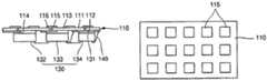
- the memory card 100includes a circuit board 110 which has a generally quadrangular configuration.
- the circuit board 110includes and insulative layer 113 which has a generally planar upper surface 111 , and an opposed, generally planar lower surface 112 .
- Formed on the lower surface 112 of insulative layer 113is an electrically conductive pattern 114 .
- the circuit board 110Formed on the upper surface 11 of the insulative layer 113 are a plurality of test I/O pads 115 .
- the conductive pattern 114is electrically connected to the I/O pads 115 by one or more conductive vias 116 which extend through the insulative layer 113 .
- the circuit board 110and in particular the insulative layer 113 thereof, may be a hardened printed circuit board, a flexible printed circuit board, or its equivalent, the present invention not being limited to any particular material for the insulative layer 113 .
- each of the I/O pads 115 disposed on the upper surface 111 of the circuit board 110may have a generally quadrangular (e.g., square) configuration. Additionally, the I/O pads 115 may arranged in a full array form, defining a plurality of rows and columns ( FIG. 2B ). However, in an alternative embodiment of the circuit board 110 shown in FIG. 2C , it is contemplated that test I/O pads 115 may be arranged in a partial array form wherein they are arranged in a single row which extends along one of the lateral peripheral edge segments of the insulative layer 113 .
- test I/O pads 115as shown in FIGS. 2B and 2C is exemplary only, and that the I/O pads 115 may be included on the upper surface 111 of the insulative layer 113 in a multiplicity of different arrangements or patterns.
- the memory card 100includes a leadframe 120 which is disposed on and attached to the lower surface 112 of the insulative layer 113 .
- the leadframe 120is also electrically connected to the circuit board 110 in a manner which will be described in more detail below.
- the leadframe 120includes a ground lead 121 which has a generally U-shaped configuration and includes a pair of partially etched distal end portions. The ground lead 121 is adhered to the lower surface 112 of the insulative layer 113 so as to extend along three of the four peripheral edge segments defined by the insulative layer 113 .
- the ground lead 121 of the leadframe 120is facilitated by a layer of adhesive 123 .
- the ground lead 121will include at least one bent portion 121 b at a predetermined section thereof.
- the bent portion 121 bis bent upwardly and is electrically connected to the conductive pattern 114 formed on the lower surface 112 of the insulative layer 113 of the circuit board 110 .
- FIG. 3AAs best seen in FIG. 3A and 3B , it is contemplated that the ground lead 121 will include at least one bent portion 121 b at a predetermined section thereof.
- the bent portion 121 bis bent upwardly and is electrically connected to the conductive pattern 114 formed on the lower surface 112 of the insulative layer 113 of the circuit board 110 .
- the adhesive 123 used to attach the leadframe 120 to the circuit board 110is applied to the ground lead 121 such that no adhesive 123 is included between the bent portion 121 b and the conductive pattern 114 , thus allowing for the electrical contact between the bent portion 120 b and such conductive pattern 114 .
- the leadframe 120includes multiple leads 122 .
- Each of the leads 122includes a bonding portion 124 , a bent portion 125 , a signal I/O pad portion 126 , and a partially etched portion 127 .
- the generally planar upper surface 124 a of the bonding portion 124 of each lead 122may be adhered to the lower surface 112 of the insulative layer 113 of the circuit board 110 through the use of an adhesive 131 .
- the bent portion 125 of each lead 122slopes downwardly from the corresponding bonding portion 124 at a predetermined angle and is of a predetermined length.
- the signal I/O pad portion 126 of each lead 122defines a generally planar lower surface 126 a and extends generally horizontally from the corresponding bent portion 125 (i.e., the lower surface 126 a extends in spaced, generally parallel relation to the upper surface 124 a of the corresponding bonding portion 124 ), and is also of a predetermined length. It is contemplated that the signal I/O pad portion 126 of each lead 122 may include a plating layer 128 which is applied to the lower surface 126 a thereof to improve the electrical connection with an external device. The plating layer 128 of each lead 122 may be formed of a material having superior conductivity.
- Exemplary materials for the plating layers 128include gold, silver or their equivalents, though the present invention is not limited to any particular material for the plating layers 128 .
- the partially etched portion 127 of each lead 122extends horizontally from the corresponding signal I/O pad portion 126 , and is also of a predetermined length.
- the generally planar upper surface of the partially etched portion 127 of each lead 122is continuous with the generally planar upper surface of the corresponding signal I/O pad portion 126 , with the lower surface of the partially etched portion 127 being vertically recessed or offset relative to the lower surface 126 a of the corresponding signal I/O pad portion 126 .
- each lead 122is used to increase the bonding force between the lead 122 and an encapsulant body of the memory card 100 in a manner which will be described in more detail below.
- the leadframe 120 of the memory card 100is preferably fabricated from a conductive metal material (e.g., copper) through either a chemical etching or mechanical stamping process.
- the memory card 100 of the first embodimentfurther comprises an electronic circuit element 130 which is attached to the lower surface 112 of the insulative layer 113 of the circuit board 110 through the use of an adhesive 131 .
- the electronic circuit element 130may comprise a semiconductor package 132 , a semiconductor die 133 , and a passive element 134 . In the absence of the passive element 134 , the semiconductor package 132 and/or the semiconductor device 133 may be adhered to the lower surface 112 of the insulative layer 113 . In this regard, though the electronic circuit element 130 is shown in FIGS.
- conductive wires 140are used to facilitate the electrical connection between the electronic circuit element 130 and the circuit board 110 , between the electronic circuit element 130 and the leads 122 of the leadframe 120 , between the electronic circuit element 130 and the ground lead 121 of the leadframe 120 , and between the individual components of the electronic circuit element 130 .
- conductive wires 140are advanced between the electronic circuit element 130 and the bonding portions 124 of the leads 122 , and between the electronic circuit element 130 and the conductive pattern 114 formed on the lower surface 112 of the insulative layer 113 of the circuit board 110 .
- a flip chip bonding methodmay be used as an alternative to conductive wires 140 to facilitate the electrical connection of the electronic circuit element 130 to the circuit board 110 and/or the leadframe 120 .
- grounding treatment for the electronic circuit element 130 , the circuit board 110 , and the leads 122may be facilitated, thereby improving the electrical performance of the electronic circuit element 130 .
- the memory card 100 of the first embodimentfurther comprises an encapsulant body 150 which at least partially encapsulates the circuit board 110 , the leadframe 120 , the electronic circuit element 130 and the conductive wires 140 to protect the same from the external environment.
- the test I/O pads 115 of the circuit board 110are exposed in the upper surface 151 of the body 150 .
- the plating layer 128 formed on the lower surface 126 a of the signal I/O pad portion 126 of each lead 122is itself exposed in the lower surface 152 of the body 150 .
- the signal I/O pads portions 126may be connected to an external device.
- the distal ends of the partially etched portions 127 of the leads 122 and the distal ends of the partially etched distal end portions of the ground lead 121are exposed in and substantially flush with a common side surface of the body 150 .
- the encapsulant material used to form the body 150may include, for example, an epoxy, a plastic molding compound, or equivalents thereto, the present invention not being limited to any specific material for the body 150 .
- a label 160will be attached to the upper surface 151 of the body 150 in a manner covering the exposed test I/O pads 115 of the circuit board 110 , thus shielding them from view. As a result, the inclusion of the test I/O pads 115 in the memory card 100 does not adversely affect the appearance thereof.
- FIGS. 5A–5Fthere is shown an exemplary sequence of steps which may be used to facilitate the fabrication of the memory card 100 of the first embodiment of the present invention.
- the above-described leadframe 120is provided ( FIG. 5A ).
- the circuit board 110is then adhered to the upper surface 121 a of the ground lead 121 of the leadframe 120 in the above-described manner through the use of the adhesive 123 ( FIG. 5B ).
- a predetermined section or area of the lower surface 112 of the insulative layer 113 of the circuit board 110may be adhered to the upper surfaces 124 a of one or more of the bonding parts 124 of the leads 122 through the use of adhesive 131 .
- the attachment of the circuit board 110 to the leadframe 120also will typically facilitate the electrical communication therebetween by virtue of the contact between the bent portion 121 b of the ground lead 121 and the conductive pattern 114 of the circuit board 110 .
- the electronic circuit element 130is adhered to the lower surface 112 of the insulative layer 113 of the circuit board 110 through the use of the adhesive 131 ( FIG. 5C ). Thereafter, the bonding wires 140 are applied in a manner facilitating the electrical connection between the electronic circuit element 130 and the leads 122 , between the electronic circuit element 130 and the circuit board 110 , between the electronic circuit element 130 and the ground lead 121 , and between the individual components of the electronic circuit element 130 ( FIG. 5D ).
- one or more conductive wires 140may be used to facilitate the electrical connection between the circuit board 110 and the ground lead 121 .
- the leadframe 120 , the circuit board 110 , the electronic circuit element 130 and the conductive wires 140are then encapsulated with the body 150 in the above-described manner ( FIG. 5E ).
- the test I/O pads 115 of the circuit board 110are exposed in the upper surface 151 of the body 150 , with the plating layers 128 formed on the signal I/O pad portions 126 of the leads 122 being exposed in the lower surface 152 of the body 150 .
- the recessed lower surfaces of the partially etched portions 127 of the leads 122 and the recessed lower surfaces of the partially etched distal end portions of the ground lead 121are each covered by the body 150 , thereby strengthening the mechanical interlock between the body 150 and the leads 121 , 122 .
- testing and programming processesare typically performed using the test I/O pads 115 .
- These processesare used to test the memory card electrically and to store desired programs necessary to facilitate desired memory functions.
- ittakes only about 30 to 40 seconds per memory card 100 to perform the programming and testing processes due to the inclusion of the test I/O pads 115 therein.
- the label 160is adhered to the body 150 in the above-described manner ( FIG. 5F ). As indicated above, the attachment of the label 160 to the body 150 effectively conceals the test I/O pads 115 , thus not detracting from the appearance of the memory card 100 .
- the leadframe 120may initially be provided in an unsignulated state wherein the partially etched portions 127 of the leads 122 and the partially etched end portions of the ground lead 121 are attached to a common dambar (not shown).
- the attachment of the leads 121 , 122 to the common dambarmaintains the same in their prescribed orientations relative to each other in the process of attaching the leadframe 120 and the circuit board 110 to each other.
- the body 150is thereafter formed such that the dambar remains exposed, and is not covered thereby.
- the dambarmay be removed from the remainder of the leadframe 120 through the completion of a singulation or severing process. As a result of such singulation, the severed ends of the leads 121 , 122 remain exposed in and substantially flush with a side surface of the body 150 .
- FIG. 4there is shown a memory card 200 constructed in accordance with a second embodiment of the present invention.
- the memory card 200 of the second embodimentbears substantially similarity in construction to the memory card 100 of the first embodiment, with the 200 series reference numerals in FIG. 4 being used to identify the same structures identified by the corresponding 100 series reference numerals included in FIGS. 1A–1D .
- the distinctions between the memory cards 200 , 100will be discussed below.
- the memory card 200differs from the memory card 100 in that the memory card 200 further includes an outer body or cap 260 which is coupled to the upper surface 251 and a side surface 253 of the body 250 .
- the test I/O pads 215 of the circuit board 210are not exposed to the exterior due to the same being effectively covered by the cap 260 .
- the distal ends of the partially etched portions 227 of the leads 222 and the distal ends of the partially etched distal end portions of the ground lead 221 which are exposed in the side surface 253 of the body 250are covered by the cap 260 , thus preventing inadvertent damage to or shorting with an external device into which the memory card 200 is advanced.
- a label 270may be adhered to the cap 260 .
- FIGS. 6A and 6Bthere is shown an exemplary sequence of steps which may be used to facilitate the fabrication of the memory card 200 of the second embodiment of the present invention.
- the method for forming the memory card 200is identical to that described above in relation to FIGS. 5A–5F regarding the steps for fabricating the memory card 100 of the first embodiment.
- the cap 260Upon the completion of the testing and programming processes on the memory card 200 , the cap 260 is attached to the body 250 in a manner covering the upper surface 251 and side surface 253 thereof.
- the cap 260itself defines an upper surface 262 and a side surface 263 , and is attached to the body 250 in a manner effectively covering and concealing the test I/O pads 215 .
- the cap 260also effectively covers and conceals the distal end portions of the partially etched portions 227 of the leads 222 and the distal ends of the partially etched distal end portions of the ground lead 221 which are exposed in the side surface 253 of the body 250 .
Landscapes
- Physics & Mathematics (AREA)
- Condensed Matter Physics & Semiconductors (AREA)
- General Physics & Mathematics (AREA)
- Engineering & Computer Science (AREA)
- Computer Hardware Design (AREA)
- Microelectronics & Electronic Packaging (AREA)
- Power Engineering (AREA)
- Credit Cards Or The Like (AREA)
Abstract
Description
Claims (20)
Priority Applications (1)
| Application Number | Priority Date | Filing Date | Title |
|---|---|---|---|
| US11/060,263US7220915B1 (en) | 2005-02-17 | 2005-02-17 | Memory card and its manufacturing method |
Applications Claiming Priority (1)
| Application Number | Priority Date | Filing Date | Title |
|---|---|---|---|
| US11/060,263US7220915B1 (en) | 2005-02-17 | 2005-02-17 | Memory card and its manufacturing method |
Publications (1)
| Publication Number | Publication Date |
|---|---|
| US7220915B1true US7220915B1 (en) | 2007-05-22 |
Family
ID=38049547
Family Applications (1)
| Application Number | Title | Priority Date | Filing Date |
|---|---|---|---|
| US11/060,263Expired - LifetimeUS7220915B1 (en) | 2005-02-17 | 2005-02-17 | Memory card and its manufacturing method |
Country Status (1)
| Country | Link |
|---|---|
| US (1) | US7220915B1 (en) |
Cited By (9)
| Publication number | Priority date | Publication date | Assignee | Title |
|---|---|---|---|---|
| US20070145972A1 (en)* | 2005-06-15 | 2007-06-28 | Albert Auburger | Integrated magnetic sensor component |
| US20090152544A1 (en)* | 2007-12-17 | 2009-06-18 | Arie Frenklakh | Disguising test pads in a semiconductor package |
| USD628202S1 (en)* | 2009-10-20 | 2010-11-30 | Sandisk Corporation | MicroSD memory card with different color surfaces |
| WO2010104543A3 (en)* | 2008-12-31 | 2010-12-02 | Arizona Board Of Regents, For And On Behalf Of Arizona State University | Integrated circuits secure from invasion and methods of manufacturing the same |
| US20110090277A1 (en)* | 2009-10-20 | 2011-04-21 | Itzhak Pomerantz | Method and System for Printing Graphical Content onto a Plurality of Memory Devices and for Providing a Visually Distinguishable Memory Device |
| USD638431S1 (en) | 2009-10-20 | 2011-05-24 | Sandisk Corporation | MicroSD memory card with a semi-transparent color surface |
| CN101690431B (en)* | 2007-06-21 | 2012-07-04 | 罗伯特.博世有限公司 | electrical components |
| WO2018063631A1 (en)* | 2016-09-28 | 2018-04-05 | Intel Corporation | Leadframe for surface mounted contact fingers |
| US20220030701A1 (en)* | 2018-10-17 | 2022-01-27 | 3M Innovative Properties Company | Encapsulated printed circuit board assembly |
Citations (33)
| Publication number | Priority date | Publication date | Assignee | Title |
|---|---|---|---|---|
| US3668299A (en) | 1971-04-29 | 1972-06-06 | Beckman Instruments Inc | Electrical circuit module and method of assembly |
| US4532419A (en) | 1982-09-09 | 1985-07-30 | Sony Corporation | Memory card having static electricity protection |
| US4905124A (en) | 1987-03-31 | 1990-02-27 | Mitsubishi Denki Kabushiki Kaisha | IC card |
| US4974120A (en) | 1989-01-12 | 1990-11-27 | Mitsubishi Denki Kabushiki Kaisha | IC card |
| JPH03112688A (en) | 1989-09-27 | 1991-05-14 | Asahi Chem Ind Co Ltd | Ic card |
| US5172214A (en) | 1991-02-06 | 1992-12-15 | Motorola, Inc. | Leadless semiconductor device and method for making the same |
| US5360992A (en) | 1991-12-20 | 1994-11-01 | Micron Technology, Inc. | Two piece assembly for the selection of pinouts and bond options on a semiconductor device |
| KR940010938B1 (en) | 1987-05-26 | 1994-11-19 | 미쯔비시 긴소꾸 가부시기가이샤 | Hexagonal-bipyramid crystalline scandium oxide powder and process for preparing the same |
| JPH0717175A (en) | 1993-06-22 | 1995-01-20 | Seiko Epson Corp | memory card |
| JPH08190615A (en) | 1995-01-09 | 1996-07-23 | Seiko Epson Corp | memory card |
| US5574309A (en) | 1991-11-25 | 1996-11-12 | Gemplus Card International | Integrated circuit card comprising means for the protection of the integrated circuit |
| US5742479A (en) | 1994-03-09 | 1998-04-21 | Seiko Epson Corporation | Card-type electronic device with plastic frame sandwiched between printed circuit board and metal panel |
| US5753532A (en) | 1995-08-30 | 1998-05-19 | Samsung Electronics Co., Ltd. | Method of manufacturing semiconductor chip package |
| US5789280A (en) | 1994-10-11 | 1998-08-04 | Motorola, Inc. | Leadframe having secured outer leads, semiconductor device using the leadframe and method of making them |
| US5808359A (en) | 1994-10-28 | 1998-09-15 | Hitachi, Ltd | Semiconductor device having a heat sink with bumpers for protecting outer leads |
| US5822190A (en) | 1996-06-11 | 1998-10-13 | Kabushiki Kaisha Toshiba | Card type memory device and a method for manufacturing the same |
| JPH10334205A (en) | 1997-05-30 | 1998-12-18 | Toshiba Corp | IC card and memory package |
| US5893724A (en) | 1995-10-28 | 1999-04-13 | Institute Of Microelectronics | Method for forming a highly reliable and planar ball grid array package |
| US5977613A (en) | 1996-03-07 | 1999-11-02 | Matsushita Electronics Corporation | Electronic component, method for making the same, and lead frame and mold assembly for use therein |
| US6040622A (en) | 1998-06-11 | 2000-03-21 | Sandisk Corporation | Semiconductor package using terminals formed on a conductive layer of a circuit board |
| US6053414A (en)* | 1996-04-22 | 2000-04-25 | Siemens Aktiengesellschaft | Data carrier card |
| US6143981A (en) | 1998-06-24 | 2000-11-07 | Amkor Technology, Inc. | Plastic integrated circuit package and method and leadframe for making the package |
| USD445096S1 (en) | 1998-04-01 | 2001-07-17 | Sandisk Corporation | Removable memory card for use with portable electronic devices |
| USD446525S1 (en) | 1999-08-24 | 2001-08-14 | Kabushiki Kaisha Toshiba | IC memory card |
| US6376283B1 (en) | 2000-04-19 | 2002-04-23 | Power Digital Card Co., Ltd. | Mono-chip multimediacard fabrication method |
| US6384472B1 (en) | 2000-03-24 | 2002-05-07 | Siliconware Precision Industries Co., Ltd | Leadless image sensor package structure and method for making the same |
| US20020140068A1 (en) | 2001-03-28 | 2002-10-03 | Ming-Hsun Lee | Leadframe-based semiconductor package for multi-media card |
| US6462273B1 (en)* | 2001-03-16 | 2002-10-08 | Micron Technology, Inc. | Semiconductor card and method of fabrication |
| US6476469B2 (en) | 2000-11-23 | 2002-11-05 | Siliconware Precision Industries Co., Ltd. | Quad flat non-leaded package structure for housing CMOS sensor |
| US6545332B2 (en) | 2001-01-17 | 2003-04-08 | Siliconware Precision Industries Co., Ltd. | Image sensor of a quad flat package |
| US6624005B1 (en) | 2000-09-06 | 2003-09-23 | Amkor Technology, Inc. | Semiconductor memory cards and method of making same |
| US6911718B1 (en)* | 2003-07-03 | 2005-06-28 | Amkor Technology, Inc. | Double downset double dambar suspended leadframe |
| US6965159B1 (en)* | 2001-09-19 | 2005-11-15 | Amkor Technology, Inc. | Reinforced lead-frame assembly for interconnecting circuits within a circuit module |
- 2005
- 2005-02-17USUS11/060,263patent/US7220915B1/ennot_activeExpired - Lifetime
Patent Citations (36)
| Publication number | Priority date | Publication date | Assignee | Title |
|---|---|---|---|---|
| US3668299A (en) | 1971-04-29 | 1972-06-06 | Beckman Instruments Inc | Electrical circuit module and method of assembly |
| US4532419A (en) | 1982-09-09 | 1985-07-30 | Sony Corporation | Memory card having static electricity protection |
| US4905124A (en) | 1987-03-31 | 1990-02-27 | Mitsubishi Denki Kabushiki Kaisha | IC card |
| KR940010938B1 (en) | 1987-05-26 | 1994-11-19 | 미쯔비시 긴소꾸 가부시기가이샤 | Hexagonal-bipyramid crystalline scandium oxide powder and process for preparing the same |
| US4974120A (en) | 1989-01-12 | 1990-11-27 | Mitsubishi Denki Kabushiki Kaisha | IC card |
| JPH03112688A (en) | 1989-09-27 | 1991-05-14 | Asahi Chem Ind Co Ltd | Ic card |
| US5172214A (en) | 1991-02-06 | 1992-12-15 | Motorola, Inc. | Leadless semiconductor device and method for making the same |
| US5574309A (en) | 1991-11-25 | 1996-11-12 | Gemplus Card International | Integrated circuit card comprising means for the protection of the integrated circuit |
| US5360992A (en) | 1991-12-20 | 1994-11-01 | Micron Technology, Inc. | Two piece assembly for the selection of pinouts and bond options on a semiconductor device |
| JPH0717175A (en) | 1993-06-22 | 1995-01-20 | Seiko Epson Corp | memory card |
| US5742479A (en) | 1994-03-09 | 1998-04-21 | Seiko Epson Corporation | Card-type electronic device with plastic frame sandwiched between printed circuit board and metal panel |
| US5784259A (en) | 1994-03-09 | 1998-07-21 | Seiko Epson Corporation | Card-type electronic device with plastic frame sandwiched between printed circuit boarding metal panel |
| US5789280A (en) | 1994-10-11 | 1998-08-04 | Motorola, Inc. | Leadframe having secured outer leads, semiconductor device using the leadframe and method of making them |
| US5808359A (en) | 1994-10-28 | 1998-09-15 | Hitachi, Ltd | Semiconductor device having a heat sink with bumpers for protecting outer leads |
| JPH08190615A (en) | 1995-01-09 | 1996-07-23 | Seiko Epson Corp | memory card |
| US5753532A (en) | 1995-08-30 | 1998-05-19 | Samsung Electronics Co., Ltd. | Method of manufacturing semiconductor chip package |
| US5893724A (en) | 1995-10-28 | 1999-04-13 | Institute Of Microelectronics | Method for forming a highly reliable and planar ball grid array package |
| US5977613A (en) | 1996-03-07 | 1999-11-02 | Matsushita Electronics Corporation | Electronic component, method for making the same, and lead frame and mold assembly for use therein |
| US6053414A (en)* | 1996-04-22 | 2000-04-25 | Siemens Aktiengesellschaft | Data carrier card |
| US5822190A (en) | 1996-06-11 | 1998-10-13 | Kabushiki Kaisha Toshiba | Card type memory device and a method for manufacturing the same |
| JPH10334205A (en) | 1997-05-30 | 1998-12-18 | Toshiba Corp | IC card and memory package |
| USD445096S1 (en) | 1998-04-01 | 2001-07-17 | Sandisk Corporation | Removable memory card for use with portable electronic devices |
| US6040622A (en) | 1998-06-11 | 2000-03-21 | Sandisk Corporation | Semiconductor package using terminals formed on a conductive layer of a circuit board |
| US6143981A (en) | 1998-06-24 | 2000-11-07 | Amkor Technology, Inc. | Plastic integrated circuit package and method and leadframe for making the package |
| USD446525S1 (en) | 1999-08-24 | 2001-08-14 | Kabushiki Kaisha Toshiba | IC memory card |
| US6384472B1 (en) | 2000-03-24 | 2002-05-07 | Siliconware Precision Industries Co., Ltd | Leadless image sensor package structure and method for making the same |
| US6376283B1 (en) | 2000-04-19 | 2002-04-23 | Power Digital Card Co., Ltd. | Mono-chip multimediacard fabrication method |
| US6624005B1 (en) | 2000-09-06 | 2003-09-23 | Amkor Technology, Inc. | Semiconductor memory cards and method of making same |
| US6476469B2 (en) | 2000-11-23 | 2002-11-05 | Siliconware Precision Industries Co., Ltd. | Quad flat non-leaded package structure for housing CMOS sensor |
| US6545332B2 (en) | 2001-01-17 | 2003-04-08 | Siliconware Precision Industries Co., Ltd. | Image sensor of a quad flat package |
| US6462273B1 (en)* | 2001-03-16 | 2002-10-08 | Micron Technology, Inc. | Semiconductor card and method of fabrication |
| US20020140068A1 (en) | 2001-03-28 | 2002-10-03 | Ming-Hsun Lee | Leadframe-based semiconductor package for multi-media card |
| US6603196B2 (en) | 2001-03-28 | 2003-08-05 | Siliconware Precision Industries Co., Ltd. | Leadframe-based semiconductor package for multi-media card |
| US6965159B1 (en)* | 2001-09-19 | 2005-11-15 | Amkor Technology, Inc. | Reinforced lead-frame assembly for interconnecting circuits within a circuit module |
| US6998702B1 (en)* | 2001-09-19 | 2006-02-14 | Amkor Technology, Inc. | Front edge chamfer feature for fully-molded memory cards |
| US6911718B1 (en)* | 2003-07-03 | 2005-06-28 | Amkor Technology, Inc. | Double downset double dambar suspended leadframe |
Cited By (18)
| Publication number | Priority date | Publication date | Assignee | Title |
|---|---|---|---|---|
| US7385394B2 (en)* | 2005-06-15 | 2008-06-10 | Infineon Technologies Ag | Integrated magnetic sensor component |
| US20070145972A1 (en)* | 2005-06-15 | 2007-06-28 | Albert Auburger | Integrated magnetic sensor component |
| US8379395B2 (en) | 2007-06-21 | 2013-02-19 | Robert Bosch Gmbh | Electrical component |
| CN101690431B (en)* | 2007-06-21 | 2012-07-04 | 罗伯特.博世有限公司 | electrical components |
| US20110156035A1 (en)* | 2007-12-17 | 2011-06-30 | Arie Frenklakh | Disguising test pads in a semiconductor package |
| US20090152544A1 (en)* | 2007-12-17 | 2009-06-18 | Arie Frenklakh | Disguising test pads in a semiconductor package |
| US7901957B2 (en) | 2007-12-17 | 2011-03-08 | Sandisk Corporation | Disguising test pads in a semiconductor package |
| US8283664B2 (en) | 2007-12-17 | 2012-10-09 | Sandisk Technologies Inc. | Disguising test pads in a semiconductor package |
| WO2010104543A3 (en)* | 2008-12-31 | 2010-12-02 | Arizona Board Of Regents, For And On Behalf Of Arizona State University | Integrated circuits secure from invasion and methods of manufacturing the same |
| US8860197B2 (en) | 2008-12-31 | 2014-10-14 | Arizona Board Of Regents, A Body Corporate Of The State Of Arizona Acting For And On Behalf Of Arizona State University | Integrated circuits secure from invasion and methods of manufacturing the same |
| USD638431S1 (en) | 2009-10-20 | 2011-05-24 | Sandisk Corporation | MicroSD memory card with a semi-transparent color surface |
| US20110090277A1 (en)* | 2009-10-20 | 2011-04-21 | Itzhak Pomerantz | Method and System for Printing Graphical Content onto a Plurality of Memory Devices and for Providing a Visually Distinguishable Memory Device |
| USD628202S1 (en)* | 2009-10-20 | 2010-11-30 | Sandisk Corporation | MicroSD memory card with different color surfaces |
| US8690283B2 (en) | 2009-10-20 | 2014-04-08 | Sandisk Il Ltd. | Method and system for printing graphical content onto a plurality of memory devices and for providing a visually distinguishable memory device |
| USRE47112E1 (en) | 2009-10-20 | 2018-11-06 | Sandisk Il Ltd. | Method and system for printing graphical content onto a plurality of memory devices and for providing a visually distinguishable memory device |
| WO2018063631A1 (en)* | 2016-09-28 | 2018-04-05 | Intel Corporation | Leadframe for surface mounted contact fingers |
| US20220030701A1 (en)* | 2018-10-17 | 2022-01-27 | 3M Innovative Properties Company | Encapsulated printed circuit board assembly |
| US11683880B2 (en)* | 2018-10-17 | 2023-06-20 | 3M Innovative Properties Company | Encapsulated printed circuit board assembly |
Similar Documents
| Publication | Publication Date | Title |
|---|---|---|
| US7293716B1 (en) | Secure digital memory card using land grid array structure | |
| US7011251B1 (en) | Die down multi-media card and method of making same | |
| US7598599B2 (en) | Semiconductor package system with substrate having different bondable heights at lead finger tips | |
| US7190062B1 (en) | Embedded leadframe semiconductor package | |
| US6670221B2 (en) | Semiconductor device having a built-in contact-type sensor and manufacturing method thereof | |
| US20090057822A1 (en) | Semiconductor component and method of manufacture | |
| US6091137A (en) | Semiconductor device substrate and method of manufacturing the same | |
| US6998702B1 (en) | Front edge chamfer feature for fully-molded memory cards | |
| US20070096265A1 (en) | Multiple die integrated circuit package | |
| US7936032B2 (en) | Film type package for fingerprint sensor | |
| US7202554B1 (en) | Semiconductor package and its manufacturing method | |
| EP1880419A1 (en) | Method of assembling semiconductor devices with leds | |
| US7633763B1 (en) | Double mold memory card and its manufacturing method | |
| US7214326B1 (en) | Increased capacity leadframe and semiconductor package using the same | |
| US7220915B1 (en) | Memory card and its manufacturing method | |
| US6963135B2 (en) | Semiconductor package for memory chips | |
| US7095103B1 (en) | Leadframe based memory card | |
| US6911718B1 (en) | Double downset double dambar suspended leadframe | |
| US7825505B2 (en) | Semiconductor package and method therefor | |
| US6897550B1 (en) | Fully-molded leadframe stand-off feature | |
| CN111554652B (en) | Conductive trace design for smart cards | |
| US7193305B1 (en) | Memory card ESC substrate insert | |
| US6717822B1 (en) | Lead-frame method and circuit module assembly including edge stiffener | |
| US20090021921A1 (en) | Memory card and its manufacturing method | |
| US7556986B1 (en) | Tape supported memory card leadframe structure |
Legal Events
| Date | Code | Title | Description |
|---|---|---|---|
| AS | Assignment | Owner name:AMKOR TECHNOLOGY, INC., ARIZONA Free format text:ASSIGNMENT OF ASSIGNORS INTEREST;ASSIGNORS:PARK, CHUL WOO;JANG, SANG JAE;PARK, SUNG SU;AND OTHERS;REEL/FRAME:016304/0064 Effective date:20050216 | |
| STCF | Information on status: patent grant | Free format text:PATENTED CASE | |
| AS | Assignment | Owner name:BANK OF AMERICA, N.A., TEXAS Free format text:PATENT SECURITY AGREEMENT;ASSIGNOR:AMKOR TECHNOLOGY, INC.;REEL/FRAME:022764/0864 Effective date:20090416 Owner name:BANK OF AMERICA, N.A.,TEXAS Free format text:PATENT SECURITY AGREEMENT;ASSIGNOR:AMKOR TECHNOLOGY, INC.;REEL/FRAME:022764/0864 Effective date:20090416 | |
| FPAY | Fee payment | Year of fee payment:4 | |
| FPAY | Fee payment | Year of fee payment:8 | |
| AS | Assignment | Owner name:BANK OF AMERICA, N.A., AS AGENT, CALIFORNIA Free format text:SECURITY INTEREST;ASSIGNOR:AMKOR TECHNOLOGY, INC.;REEL/FRAME:046683/0139 Effective date:20180713 | |
| MAFP | Maintenance fee payment | Free format text:PAYMENT OF MAINTENANCE FEE, 12TH YEAR, LARGE ENTITY (ORIGINAL EVENT CODE: M1553); ENTITY STATUS OF PATENT OWNER: LARGE ENTITY Year of fee payment:12 | |
| AS | Assignment | Owner name:AMKOR TECHNOLOGY SINGAPORE HOLDING PTE.LTD., SINGAPORE Free format text:ASSIGNMENT OF ASSIGNORS INTEREST;ASSIGNOR:AMKOR TECHNOLOGY, INC.;REEL/FRAME:054067/0135 Effective date:20191119 |