US7220673B2 - Method for depositing tungsten-containing layers by vapor deposition techniques - Google Patents
Method for depositing tungsten-containing layers by vapor deposition techniquesDownload PDFInfo
- Publication number
- US7220673B2 US7220673B2US11/461,909US46190906AUS7220673B2US 7220673 B2US7220673 B2US 7220673B2US 46190906 AUS46190906 AUS 46190906AUS 7220673 B2US7220673 B2US 7220673B2
- Authority
- US
- United States
- Prior art keywords
- tungsten
- substrate
- layer
- gas
- processing
- Prior art date
- Legal status (The legal status is an assumption and is not a legal conclusion. Google has not performed a legal analysis and makes no representation as to the accuracy of the status listed.)
- Expired - Lifetime
Links
- 238000000034methodMethods0.000titleclaimsabstractdescription84
- WFKWXMTUELFFGS-UHFFFAOYSA-NtungstenChemical compound[W]WFKWXMTUELFFGS-UHFFFAOYSA-N0.000titleclaimsabstractdescription77
- 229910052721tungstenInorganic materials0.000titleclaimsabstractdescription77
- 239000010937tungstenSubstances0.000titleclaimsabstractdescription77
- 238000000151depositionMethods0.000titleclaimsdescription53
- 238000007740vapor depositionMethods0.000titledescription2
- 239000000758substrateSubstances0.000claimsabstractdescription90
- 230000006911nucleationEffects0.000claimsabstractdescription33
- 238000010899nucleationMethods0.000claimsabstractdescription33
- 238000000231atomic layer depositionMethods0.000claimsabstractdescription28
- 230000008569processEffects0.000claimsabstractdescription25
- 238000005229chemical vapour depositionMethods0.000claimsabstractdescription20
- 239000012713reactive precursorSubstances0.000claimsabstractdescription16
- 239000000463materialSubstances0.000claimsabstractdescription13
- 230000004888barrier functionEffects0.000claimsabstractdescription12
- 229910052796boronInorganic materials0.000claimsabstractdescription11
- VYPSYNLAJGMNEJ-UHFFFAOYSA-NSilicium dioxideChemical compoundO=[Si]=OVYPSYNLAJGMNEJ-UHFFFAOYSA-N0.000claimsabstractdescription7
- NRTOMJZYCJJWKI-UHFFFAOYSA-NTitanium nitrideChemical compound[Ti]#NNRTOMJZYCJJWKI-UHFFFAOYSA-N0.000claimsabstractdescription6
- RTAQQCXQSZGOHL-UHFFFAOYSA-NTitaniumChemical compound[Ti]RTAQQCXQSZGOHL-UHFFFAOYSA-N0.000claimsabstractdescription5
- 239000010936titaniumSubstances0.000claimsabstractdescription5
- 229910052719titaniumInorganic materials0.000claimsabstractdescription5
- ZOXJGFHDIHLPTG-UHFFFAOYSA-NBoronChemical compound[B]ZOXJGFHDIHLPTG-UHFFFAOYSA-N0.000claimsabstract10
- 229910052814silicon oxideInorganic materials0.000claimsabstract5
- 239000007789gasSubstances0.000claimsdescription83
- NXHILIPIEUBEPD-UHFFFAOYSA-Htungsten hexafluorideChemical compoundF[W](F)(F)(F)(F)FNXHILIPIEUBEPD-UHFFFAOYSA-H0.000claimsdescription15
- XKRFYHLGVUSROY-UHFFFAOYSA-NArgonChemical compound[Ar]XKRFYHLGVUSROY-UHFFFAOYSA-N0.000claimsdescription14
- XUIMIQQOPSSXEZ-UHFFFAOYSA-NSiliconChemical compound[Si]XUIMIQQOPSSXEZ-UHFFFAOYSA-N0.000claimsdescription9
- 229910052710siliconInorganic materials0.000claimsdescription9
- 239000010703siliconSubstances0.000claimsdescription9
- 229910052786argonInorganic materials0.000claimsdescription7
- BLRPTPMANUNPDV-UHFFFAOYSA-NSilaneChemical compound[SiH4]BLRPTPMANUNPDV-UHFFFAOYSA-N0.000claimsdescription4
- 239000001257hydrogenSubstances0.000claimsdescription4
- 229910052739hydrogenInorganic materials0.000claimsdescription4
- 125000004435hydrogen atomChemical class[H]*0.000claimsdescription4
- 229910000077silaneInorganic materials0.000claimsdescription4
- 238000005019vapor deposition processMethods0.000claims2
- QJGQUHMNIGDVPM-UHFFFAOYSA-Nnitrogen groupChemical group[N]QJGQUHMNIGDVPM-UHFFFAOYSA-N0.000claims1
- 239000003989dielectric materialSubstances0.000abstract1
- 239000010410layerSubstances0.000description81
- 230000008021depositionEffects0.000description31
- NJPPVKZQTLUDBO-UHFFFAOYSA-NnovaluronChemical compoundC1=C(Cl)C(OC(F)(F)C(OC(F)(F)F)F)=CC=C1NC(=O)NC(=O)C1=C(F)C=CC=C1FNJPPVKZQTLUDBO-UHFFFAOYSA-N0.000description16
- 239000003870refractory metalSubstances0.000description14
- 238000010926purgeMethods0.000description11
- 238000004891communicationMethods0.000description8
- 239000004065semiconductorSubstances0.000description8
- 239000012159carrier gasSubstances0.000description7
- 125000004429atomChemical group0.000description4
- 230000008901benefitEffects0.000description4
- 230000015572biosynthetic processEffects0.000description4
- 239000000203mixtureSubstances0.000description4
- 150000001875compoundsChemical class0.000description3
- 230000001419dependent effectEffects0.000description3
- 238000005137deposition processMethods0.000description3
- 238000002347injectionMethods0.000description3
- 239000007924injectionSubstances0.000description3
- 230000010354integrationEffects0.000description3
- 239000003446ligandSubstances0.000description3
- 238000005240physical vapour depositionMethods0.000description3
- 238000003877atomic layer epitaxyMethods0.000description2
- 238000004590computer programMethods0.000description2
- 230000001351cycling effectEffects0.000description2
- 239000012530fluidSubstances0.000description2
- 230000006870functionEffects0.000description2
- 238000004519manufacturing processMethods0.000description2
- 238000005086pumpingMethods0.000description2
- 239000002356single layerSubstances0.000description2
- 229940126062Compound ADrugs0.000description1
- NLDMNSXOCDLTTB-UHFFFAOYSA-NHeterophylliin ANatural productsO1C2COC(=O)C3=CC(O)=C(O)C(O)=C3C3=C(O)C(O)=C(O)C=C3C(=O)OC2C(OC(=O)C=2C=C(O)C(O)=C(O)C=2)C(O)C1OC(=O)C1=CC(O)=C(O)C(O)=C1NLDMNSXOCDLTTB-UHFFFAOYSA-N0.000description1
- 239000000654additiveSubstances0.000description1
- 230000000996additive effectEffects0.000description1
- 238000006243chemical reactionMethods0.000description1
- 229910052681coesiteInorganic materials0.000description1
- 239000004020conductorSubstances0.000description1
- 230000001276controlling effectEffects0.000description1
- 229910052906cristobaliteInorganic materials0.000description1
- 238000006073displacement reactionMethods0.000description1
- 230000000694effectsEffects0.000description1
- 238000005516engineering processMethods0.000description1
- 230000004907fluxEffects0.000description1
- 239000008246gaseous mixtureSubstances0.000description1
- 239000011261inert gasSubstances0.000description1
- 230000007246mechanismEffects0.000description1
- 238000000206photolithographyMethods0.000description1
- 239000002243precursorSubstances0.000description1
- 238000004886process controlMethods0.000description1
- 238000002310reflectometryMethods0.000description1
- 230000001105regulatory effectEffects0.000description1
- 229920006395saturated elastomerPolymers0.000description1
- 239000000377silicon dioxideSubstances0.000description1
- 229910052682stishoviteInorganic materials0.000description1
- 238000003860storageMethods0.000description1
- MAKDTFFYCIMFQP-UHFFFAOYSA-Ntitanium tungstenChemical compound[Ti].[W]MAKDTFFYCIMFQP-UHFFFAOYSA-N0.000description1
- 238000012876topographyMethods0.000description1
- 229910052905tridymiteInorganic materials0.000description1
Images


Classifications
- C—CHEMISTRY; METALLURGY
- C23—COATING METALLIC MATERIAL; COATING MATERIAL WITH METALLIC MATERIAL; CHEMICAL SURFACE TREATMENT; DIFFUSION TREATMENT OF METALLIC MATERIAL; COATING BY VACUUM EVAPORATION, BY SPUTTERING, BY ION IMPLANTATION OR BY CHEMICAL VAPOUR DEPOSITION, IN GENERAL; INHIBITING CORROSION OF METALLIC MATERIAL OR INCRUSTATION IN GENERAL
- C23C—COATING METALLIC MATERIAL; COATING MATERIAL WITH METALLIC MATERIAL; SURFACE TREATMENT OF METALLIC MATERIAL BY DIFFUSION INTO THE SURFACE, BY CHEMICAL CONVERSION OR SUBSTITUTION; COATING BY VACUUM EVAPORATION, BY SPUTTERING, BY ION IMPLANTATION OR BY CHEMICAL VAPOUR DEPOSITION, IN GENERAL
- C23C16/00—Chemical coating by decomposition of gaseous compounds, without leaving reaction products of surface material in the coating, i.e. chemical vapour deposition [CVD] processes
- C23C16/02—Pretreatment of the material to be coated
- C23C16/0272—Deposition of sub-layers, e.g. to promote the adhesion of the main coating
- C—CHEMISTRY; METALLURGY
- C23—COATING METALLIC MATERIAL; COATING MATERIAL WITH METALLIC MATERIAL; CHEMICAL SURFACE TREATMENT; DIFFUSION TREATMENT OF METALLIC MATERIAL; COATING BY VACUUM EVAPORATION, BY SPUTTERING, BY ION IMPLANTATION OR BY CHEMICAL VAPOUR DEPOSITION, IN GENERAL; INHIBITING CORROSION OF METALLIC MATERIAL OR INCRUSTATION IN GENERAL
- C23C—COATING METALLIC MATERIAL; COATING MATERIAL WITH METALLIC MATERIAL; SURFACE TREATMENT OF METALLIC MATERIAL BY DIFFUSION INTO THE SURFACE, BY CHEMICAL CONVERSION OR SUBSTITUTION; COATING BY VACUUM EVAPORATION, BY SPUTTERING, BY ION IMPLANTATION OR BY CHEMICAL VAPOUR DEPOSITION, IN GENERAL
- C23C16/00—Chemical coating by decomposition of gaseous compounds, without leaving reaction products of surface material in the coating, i.e. chemical vapour deposition [CVD] processes
- C23C16/22—Chemical coating by decomposition of gaseous compounds, without leaving reaction products of surface material in the coating, i.e. chemical vapour deposition [CVD] processes characterised by the deposition of inorganic material, other than metallic material
- C23C16/30—Deposition of compounds, mixtures or solid solutions, e.g. borides, carbides, nitrides
- C23C16/34—Nitrides
- C—CHEMISTRY; METALLURGY
- C23—COATING METALLIC MATERIAL; COATING MATERIAL WITH METALLIC MATERIAL; CHEMICAL SURFACE TREATMENT; DIFFUSION TREATMENT OF METALLIC MATERIAL; COATING BY VACUUM EVAPORATION, BY SPUTTERING, BY ION IMPLANTATION OR BY CHEMICAL VAPOUR DEPOSITION, IN GENERAL; INHIBITING CORROSION OF METALLIC MATERIAL OR INCRUSTATION IN GENERAL
- C23C—COATING METALLIC MATERIAL; COATING MATERIAL WITH METALLIC MATERIAL; SURFACE TREATMENT OF METALLIC MATERIAL BY DIFFUSION INTO THE SURFACE, BY CHEMICAL CONVERSION OR SUBSTITUTION; COATING BY VACUUM EVAPORATION, BY SPUTTERING, BY ION IMPLANTATION OR BY CHEMICAL VAPOUR DEPOSITION, IN GENERAL
- C23C16/00—Chemical coating by decomposition of gaseous compounds, without leaving reaction products of surface material in the coating, i.e. chemical vapour deposition [CVD] processes
- C23C16/44—Chemical coating by decomposition of gaseous compounds, without leaving reaction products of surface material in the coating, i.e. chemical vapour deposition [CVD] processes characterised by the method of coating
- C23C16/455—Chemical coating by decomposition of gaseous compounds, without leaving reaction products of surface material in the coating, i.e. chemical vapour deposition [CVD] processes characterised by the method of coating characterised by the method used for introducing gases into reaction chamber or for modifying gas flows in reaction chamber
- C23C16/45523—Pulsed gas flow or change of composition over time
- C23C16/45525—Atomic layer deposition [ALD]
- C23C16/45527—Atomic layer deposition [ALD] characterized by the ALD cycle, e.g. different flows or temperatures during half-reactions, unusual pulsing sequence, use of precursor mixtures or auxiliary reactants or activations
- C—CHEMISTRY; METALLURGY
- C23—COATING METALLIC MATERIAL; COATING MATERIAL WITH METALLIC MATERIAL; CHEMICAL SURFACE TREATMENT; DIFFUSION TREATMENT OF METALLIC MATERIAL; COATING BY VACUUM EVAPORATION, BY SPUTTERING, BY ION IMPLANTATION OR BY CHEMICAL VAPOUR DEPOSITION, IN GENERAL; INHIBITING CORROSION OF METALLIC MATERIAL OR INCRUSTATION IN GENERAL
- C23C—COATING METALLIC MATERIAL; COATING MATERIAL WITH METALLIC MATERIAL; SURFACE TREATMENT OF METALLIC MATERIAL BY DIFFUSION INTO THE SURFACE, BY CHEMICAL CONVERSION OR SUBSTITUTION; COATING BY VACUUM EVAPORATION, BY SPUTTERING, BY ION IMPLANTATION OR BY CHEMICAL VAPOUR DEPOSITION, IN GENERAL
- C23C16/00—Chemical coating by decomposition of gaseous compounds, without leaving reaction products of surface material in the coating, i.e. chemical vapour deposition [CVD] processes
- C23C16/44—Chemical coating by decomposition of gaseous compounds, without leaving reaction products of surface material in the coating, i.e. chemical vapour deposition [CVD] processes characterised by the method of coating
- C23C16/455—Chemical coating by decomposition of gaseous compounds, without leaving reaction products of surface material in the coating, i.e. chemical vapour deposition [CVD] processes characterised by the method of coating characterised by the method used for introducing gases into reaction chamber or for modifying gas flows in reaction chamber
- C23C16/45561—Gas plumbing upstream of the reaction chamber
- C—CHEMISTRY; METALLURGY
- C30—CRYSTAL GROWTH
- C30B—SINGLE-CRYSTAL GROWTH; UNIDIRECTIONAL SOLIDIFICATION OF EUTECTIC MATERIAL OR UNIDIRECTIONAL DEMIXING OF EUTECTOID MATERIAL; REFINING BY ZONE-MELTING OF MATERIAL; PRODUCTION OF A HOMOGENEOUS POLYCRYSTALLINE MATERIAL WITH DEFINED STRUCTURE; SINGLE CRYSTALS OR HOMOGENEOUS POLYCRYSTALLINE MATERIAL WITH DEFINED STRUCTURE; AFTER-TREATMENT OF SINGLE CRYSTALS OR A HOMOGENEOUS POLYCRYSTALLINE MATERIAL WITH DEFINED STRUCTURE; APPARATUS THEREFOR
- C30B25/00—Single-crystal growth by chemical reaction of reactive gases, e.g. chemical vapour-deposition growth
- C30B25/02—Epitaxial-layer growth
- C30B25/14—Feed and outlet means for the gases; Modifying the flow of the reactive gases
- C—CHEMISTRY; METALLURGY
- C30—CRYSTAL GROWTH
- C30B—SINGLE-CRYSTAL GROWTH; UNIDIRECTIONAL SOLIDIFICATION OF EUTECTIC MATERIAL OR UNIDIRECTIONAL DEMIXING OF EUTECTOID MATERIAL; REFINING BY ZONE-MELTING OF MATERIAL; PRODUCTION OF A HOMOGENEOUS POLYCRYSTALLINE MATERIAL WITH DEFINED STRUCTURE; SINGLE CRYSTALS OR HOMOGENEOUS POLYCRYSTALLINE MATERIAL WITH DEFINED STRUCTURE; AFTER-TREATMENT OF SINGLE CRYSTALS OR A HOMOGENEOUS POLYCRYSTALLINE MATERIAL WITH DEFINED STRUCTURE; APPARATUS THEREFOR
- C30B29/00—Single crystals or homogeneous polycrystalline material with defined structure characterised by the material or by their shape
- C30B29/10—Inorganic compounds or compositions
- C30B29/38—Nitrides
- H—ELECTRICITY
- H01—ELECTRIC ELEMENTS
- H01L—SEMICONDUCTOR DEVICES NOT COVERED BY CLASS H10
- H01L21/00—Processes or apparatus adapted for the manufacture or treatment of semiconductor or solid state devices or of parts thereof
- H01L21/02—Manufacture or treatment of semiconductor devices or of parts thereof
- H01L21/04—Manufacture or treatment of semiconductor devices or of parts thereof the devices having potential barriers, e.g. a PN junction, depletion layer or carrier concentration layer
- H01L21/18—Manufacture or treatment of semiconductor devices or of parts thereof the devices having potential barriers, e.g. a PN junction, depletion layer or carrier concentration layer the devices having semiconductor bodies comprising elements of Group IV of the Periodic Table or AIIIBV compounds with or without impurities, e.g. doping materials
- H01L21/28—Manufacture of electrodes on semiconductor bodies using processes or apparatus not provided for in groups H01L21/20 - H01L21/268
- H01L21/283—Deposition of conductive or insulating materials for electrodes conducting electric current
- H01L21/285—Deposition of conductive or insulating materials for electrodes conducting electric current from a gas or vapour, e.g. condensation
- H01L21/28506—Deposition of conductive or insulating materials for electrodes conducting electric current from a gas or vapour, e.g. condensation of conductive layers
- H01L21/28512—Deposition of conductive or insulating materials for electrodes conducting electric current from a gas or vapour, e.g. condensation of conductive layers on semiconductor bodies comprising elements of Group IV of the Periodic Table
- H01L21/28556—Deposition of conductive or insulating materials for electrodes conducting electric current from a gas or vapour, e.g. condensation of conductive layers on semiconductor bodies comprising elements of Group IV of the Periodic Table by chemical means, e.g. CVD, LPCVD, PECVD, laser CVD
- H01L21/28562—Selective deposition
- H—ELECTRICITY
- H01—ELECTRIC ELEMENTS
- H01L—SEMICONDUCTOR DEVICES NOT COVERED BY CLASS H10
- H01L21/00—Processes or apparatus adapted for the manufacture or treatment of semiconductor or solid state devices or of parts thereof
- H01L21/70—Manufacture or treatment of devices consisting of a plurality of solid state components formed in or on a common substrate or of parts thereof; Manufacture of integrated circuit devices or of parts thereof
- H01L21/71—Manufacture of specific parts of devices defined in group H01L21/70
- H01L21/768—Applying interconnections to be used for carrying current between separate components within a device comprising conductors and dielectrics
- H01L21/76838—Applying interconnections to be used for carrying current between separate components within a device comprising conductors and dielectrics characterised by the formation and the after-treatment of the conductors
- H01L21/76841—Barrier, adhesion or liner layers
- H01L21/76843—Barrier, adhesion or liner layers formed in openings in a dielectric
- H—ELECTRICITY
- H01—ELECTRIC ELEMENTS
- H01L—SEMICONDUCTOR DEVICES NOT COVERED BY CLASS H10
- H01L21/00—Processes or apparatus adapted for the manufacture or treatment of semiconductor or solid state devices or of parts thereof
- H01L21/70—Manufacture or treatment of devices consisting of a plurality of solid state components formed in or on a common substrate or of parts thereof; Manufacture of integrated circuit devices or of parts thereof
- H01L21/71—Manufacture of specific parts of devices defined in group H01L21/70
- H01L21/768—Applying interconnections to be used for carrying current between separate components within a device comprising conductors and dielectrics
- H01L21/76838—Applying interconnections to be used for carrying current between separate components within a device comprising conductors and dielectrics characterised by the formation and the after-treatment of the conductors
- H01L21/76841—Barrier, adhesion or liner layers
- H01L21/76871—Layers specifically deposited to enhance or enable the nucleation of further layers, i.e. seed layers
- H01L21/76876—Layers specifically deposited to enhance or enable the nucleation of further layers, i.e. seed layers for deposition from the gas phase, e.g. CVD
- H—ELECTRICITY
- H01—ELECTRIC ELEMENTS
- H01L—SEMICONDUCTOR DEVICES NOT COVERED BY CLASS H10
- H01L21/00—Processes or apparatus adapted for the manufacture or treatment of semiconductor or solid state devices or of parts thereof
- H01L21/70—Manufacture or treatment of devices consisting of a plurality of solid state components formed in or on a common substrate or of parts thereof; Manufacture of integrated circuit devices or of parts thereof
- H01L21/71—Manufacture of specific parts of devices defined in group H01L21/70
- H01L21/768—Applying interconnections to be used for carrying current between separate components within a device comprising conductors and dielectrics
- H01L21/76838—Applying interconnections to be used for carrying current between separate components within a device comprising conductors and dielectrics characterised by the formation and the after-treatment of the conductors
- H01L21/76877—Filling of holes, grooves or trenches, e.g. vias, with conductive material
Definitions
- This inventionrelates to the processing of semiconductor substrates. More particularly, this invention relates to improvements in the process of depositing refractory metal layers on semiconductor substrates.
- CVDChemical Vapor Deposition
- ALDAtomic Layer Deposition
- ALDis based upon Atomic Layer Epitaxy (ALE) that was employed originally to fabricate electroluminescent displays.
- ALEAtomic Layer Epitaxy
- ALDemploys chemisorption to deposit a saturated monolayer of reactive precursor molecules on a substrate surface. This is achieved by alternatingly pulsing an appropriate reactive precursor into a deposition chamber. Each injection of a reactive precursor is separated by an inert gas purge to provide a new atomic layer additive to previously deposited layers to form a uniform layer on the substrate. The cycle is repeated to form the layer to a desired thickness.
- a drawback with ALD techniquesis that the deposition rate is much lower than typical CVD techniques by at least one order of magnitude.
- tungstenby traditional CVD methods, however, is attendant with several disadvantages. For example, blanket deposition of a tungsten layer on a semiconductor wafer is time-consuming at temperatures below 400° C. The deposition rate of tungsten may be improved by increasing the deposition temperature to, e.g., about 500° C. to about 550° C.; however, temperatures in this higher range may compromise the structural and operational integrity of the underlying portions of the integrated circuit being formed. Use of tungsten has also frustrated photolithography steps during the manufacturing process as it results in a relatively rough surface having a reflectivity of 20% or less than that of a silicon substrate. Finally, tungsten has proven difficult to deposit uniformly. Variance in film thickness of greater than 1% has been shown with tungsten, thereby frustrating control of the resistivity of the layer. Several prior attempts to overcome the aforementioned drawbacks have been attempted.
- a methodis disclosed to improve, inter alia, uniformity of tungsten layers by varying the deposition chemistry.
- the methodincludes, in pertinent part, formation of a nucleation layer over an intermediate barrier, layer before depositing the tungsten layer via bulk deposition.
- the nucleation layeris formed from a gaseous mixture of tungsten hexafluoride, hydrogen, silane, and argon.
- the nucleation layeris described as providing a layer of growth sites to promote uniform deposition of a tungsten layer thereon.
- the benefits provided by the nucleation layerare described as being dependent upon the barrier layer present.
- the tungsten layer's thickness uniformityis improved as much as 15%.
- the barrier layer formed from sputtered tungsten or sputtered titanium tungstenthe benefits provided by the nucleation layer are not as pronounced.
- U.S. Pat. No. 5,879,459 to Gadgil et al.discloses an apparatus that takes advantage of ALD.
- the apparatusa low profile, compact atomic layer deposition reactor (LP-CAR)
- LP-CARlow profile, compact atomic layer deposition reactor
- the apparatushas a body with a substrate processing region adapted to serve a single substrate or a planar array of substrates, as well as a valve, and a port for substrate loading and unloading.
- multiple reactorsare stacked vertically and share a common robotic handler interface with a CVD system. In this manner, the robotic handler may manipulate substrates associated with both the CVD system and the LP-CAR.
- the compact reactoris distinguished by having individual injectors, each of which comprises a charge tube formed between a charge valve and an injection valve.
- the charge valveconnects the charge tube to a pressure regulated supply, and the injection valve opens the charge tube into the compact reactor. Rapidly cycling the valves injects fixed mass-charges of gas or vapor into the compact reactor.
- a method and system to form a refractory metal layer on a substratefeatures nucleating a substrate using sequential deposition techniques in which the substrate is serially exposed to first and second reactive gases followed by forming a layer, employing vapor deposition, to subject the nucleation layer to a bulk deposition of a compound contained in one of the first and second reactive gases.
- the systemincludes a processing chamber that has a holder disposed therein to support the substrate.
- a gas delivery system and a pressure control systemis in fluid communication with the processing chamber.
- a temperature control systemis in thermal communication therewith.
- a controlleris in electrical communication with gas delivery systems, temperature control systems, pressure control systems.
- a memoryis in data communication with the controller.
- the memorycomprises a computer-readable medium having a computer-readable program embodied therein.
- the computer readable programincludes instructions for controlling the operation of the processing chamber.
- FIG. 1is a perspective view of a semiconductor processing system in accordance with the present invention
- FIG. 2is a detailed view of the processing chambers shown in FIG. 1 ;
- FIG. 3is a schematic view showing deposition of a first molecule onto a substrate during ALD
- FIG. 4is a schematic view showing deposition of second molecule onto a substrate during ALD to form a refractory metal layer
- FIG. 5is a graphical representation showing the concentration of gases, introduced into the processing chamber shown in FIG. 2 , and the time in which the gases are present in the processing chamber, in accordance with the present invention
- FIG. 6is a graphical representation showing the relationship between the number of ALD cycles and the thickness of a layer formed on a substrate employing ALD, in accordance with the present invention
- FIG. 7is a graphical representation showing the relationship between the number of ALD cycles and the resistivity of a layer formed on a substrate employing ALD, in accordance with the present invention.
- FIG. 8is a graphical representation showing the relationship between the deposition rate of a layer formed on a substrate employing ALD and the temperature of the substrate;
- FIG. 9is a graphical representation showing the relationship between the resistivity of a layer formed on a substrate employing ALD and the temperature of the substrate, in accordance with the present invention.
- FIG. 10is a cross-sectional view of a patterned substrate having a nucleation layer formed thereon employing ALD, in accordance with the present invention.
- FIG. 11is a partial cross-sectional view of the substrate, shown in FIG. 10 , with a refractory metal layer formed atop of the nucleation layer employing CVD, in accordance with the present invention.
- FIG. 12is a graphical representation showing the concentration of gases shown in FIG. 3 , in accordance with a first alternate embodiment of the present invention.
- an exemplary wafer processing systemincludes one or more processing chambers 12 and 14 disposed in a common work area 16 surrounded by a wall 18 .
- the processing chambers 12 and 14are in data communication with a controller 22 that is connected to one or more monitors, shown as 24 and 26 .
- the monitorstypically display common information concerning the process associated with the processing chambers 12 and 14 .
- One of the monitors 26is mounted to the wall 18 , with the remaining monitor 24 being disposed in the work area 16 .
- Operational control of the processing chambers 12 and 14may be achieved by the use of a light pen, associated with one of the monitors 24 and 26 , to communicate with the controller 22 .
- light pen 28is associated with monitor 24 and facilitates communication with the controller 22 through monitor 24 .
- Light pen 29facilitates communication with the controller 22 through monitor 26 .
- each of the processing chambers 12 and 14includes a housing 30 having a base wall 32 , a cover 34 , disposed opposite to the base wall 32 , and a sidewall 36 , extending therebetween.
- the housing 30defines a chamber 37 , and a pedestal 38 is disposed within the processing chamber 37 to support a substrate 42 , such as a semiconductor wafer.
- the pedestal 38may be mounted to move between the cover 34 and the base wall 32 , using a displacement mechanism (not shown), but the position thereof is typically fixed.
- Supplies of processing gases 39 a , 39 b , and 39 care in fluid communication with the processing chamber 37 via a showerhead 40 . Regulation of the flow of gases from the supplies 39 a , 39 b , and 39 c is effectuated via flow valves 41 .
- the substrate 42may be heated to a desired temperature prior to layer deposition via a heater embedded within the pedestal 38 .
- the pedestal 38may be resistively heated by applying an electric current from an AC power supply 43 to the heater element 44 .
- the substrate 42is, in turn, heated by the pedestal 38 , and can be maintained within a desired process temperature range of, for example, about 20° C. to about 750° C.
- a temperature sensor 46such as a thermocouple, is also embedded in the wafer support pedestal 38 to monitor the temperature of the pedestal 38 in a conventional manner.
- the measured temperaturemay be used in a feedback loop to control the electrical current applied to the heater element 44 by the power supply 43 such that the substrate temperature can be maintained or controlled at a desired temperature that is suitable for the particular process application.
- the pedestal 38may be heated using radiant heat (not shown).
- a vacuum pump 48is used to evacuate the processing chamber 37 and to help maintain the proper gas flows and pressure inside the processing chamber 37 .
- one or both of the processing chambers 12 and 14may operate to deposit refractory metal layers on the substrate employing sequential deposition techniques.
- sequential deposition techniquesin accordance with the present invention includes atomic layer deposition (ALD).
- ALDatomic layer deposition
- the refractory metal layermay be deposited on the material from which the substrate 42 is fabricated, e.g., SiO 2 .
- the refractory metal layermay also be deposited on a layer previously formed on the substrate 42 , e.g., titanium, titanium nitride and the like.
- a batch of a first processing gasresults in a layer of A being deposited on the substrate 42 having a surface of ligand a exposed to the processing chamber 37 .
- a purge gasenters the processing chamber 37 to purge the gas Aa x .
- a second batch of processing gas, Bb yis introduced into the processing chamber 37 .
- the a ligand present on the substrate surfacereacts with the b ligand and B atom on the releasing molecules ab and Ba, that move away from the substrate 42 and are subsequently pumped from the processing chamber 37 .
- the composition of the layer of A compoundmay be a monolayer of atoms typically formed employing ALD techniques.
- the layer of compound Amay include a layer of multiple atoms.
- the first processing gasesmay include a mixture of process gases each of which has atoms that would adhere to the substrate 42 . The process proceeds cycle after cycle, until the desired thickness is achieved.
- the processing gas Aa xincludes WF 6 and the processing gas Bb y is B 2 H 6 .
- Two purge gasesare employed: Ar and N 2 .
- Each of the processing gaseswas flowed into the processing chamber 37 with a carrier gas, which in this example were one of the purge gases: WF 6 is introduced with Ar and B 2 H 6 is introduced with N 2 .
- WF 6is introduced with Ar
- B 2 H 6is introduced with N 2 .
- the purge gasmay differ from the carrier gas, discussed more fully below.
- One cycle of the ALD technique in accordance with the present inventionincludes flowing the purge gas, N 2 , into the processing chamber 37 during time t 1 , which is approximately 0.01 seconds to 15 seconds before B 2 H 6 is flowed into the processing chamber 37 .
- the processing gas B 2 H 6is flowed into the processing chamber 37 for a time in the range of 0.01 seconds to 15 seconds, along with a carrier gas, which in this example is N 2 .
- a carrier gaswhich in this example is N 2 .
- the flow of B 2 H 6terminates and the flow of N 2 continues during time t 3 for an additional time in the range of 0.01 seconds to 15 seconds, purging the processing chamber of B 2 H 6 .
- the processing chamber 37is pumped so as to remove most, if not all, gases.
- the carrier gas Aris introduced for a time in the range of 0.01 seconds to 15 seconds during time t 5 , after which time the process gas WF 6 is introduced into the processing chamber 37 , along with the carrier gas Ar during time t 6 .
- the time t 6lasts between 0.01 seconds to 15 seconds.
- the flow of the processing gas WF 6 into the processing chamber 37is terminated approximately 0.01 seconds to 15 seconds after it commenced.
- the flow of Arcontinues for an additional time in the range of 0.01 seconds to 15 seconds, during time t 7 .
- the processing chamber 37is pumped so as to remove most, if not all, gases therein, during time t 8 .
- the pumping processlasts approximately thirty seconds, thereby concluding one cycle of the sequential deposition technique in accordance with the present invention.
- the benefits of employing the sequential deposition techniqueare manifold, including flux-independence of layer formation that provides uniformity of deposition independent of the size of a substrate. For example, the measured difference of the layer uniformity and thickness measured between a 200 mm substrate and a 32 mm substrate deposited in the same chamber is negligible. This is due to the self-limiting characteristics of the sequential deposition techniques. Further, this technique contributes to a near-perfect step coverage over complex topography.
- the thickness of the layer Bmay be easily controlled while minimizing the resistance of the same by employing sequential deposition techniques.
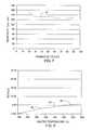
- FIG. 6it is seen in the slope of line 50 that the thickness of the tungsten layer B is proportional to the number of cycles employed to form the same.
- the resistivity of the tungsten layeris relatively independent of the thickness of the layer, as shown by the slope of line 52 in FIG. 7 .
- the thickness of a refractory metal layermay be easily controlled as a function of the cycling of the process gases introduced into the processing chamber with a negligible effect on the resistivity.
- control of the deposition ratewas found to be dependent upon the temperature of the substrate 42 .
- increasing the temperature of the substrate 42increased the deposition rate of the tungsten layer B.
- the deposition rateis shown to be approximately 2 ⁇ /cycle at a temperature of 250° C.
- the deposition rateis approximately 5 ⁇ /cycle at a temperature of 450° C.
- the resistivity of the tungsten layeris virtually independent of the layer thickness, as shown by the slope of curve 58 , shown in FIG. 9 .
- the deposition rate of the tungsten layermay be controlled as a function of temperature without compromising the resistivity of the same. However, it may be desired to reduce the time necessary to deposit an entire layer of a refractory metal.
- a bulk deposition of the refractory metal layermay be included in the deposition process.
- the bulk deposition of the refractory metaloccurs after the nucleation layer is formed in a common processing chamber.
- nucleation of a tungsten layeroccurs in chamber 12 employing the sequential deposition techniques discussed above, with the substrate 42 being heated in the range of 200° C. to 400° C., and the processing chamber 37 being pressurized in the range of 1 Torr to 10 Torr.
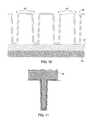
- a nucleation layer 60 of approximately 12 nm to 20 nmis formed on a patterned substrate 42 , shown in FIG. 10 .
- the substrate 42includes a barrier layer 61 and a patterned layer having a plurality of vias 63 .
- the nucleation layeris formed adjacent to the patterned layer covering the vias 63 .
- forming the nucleation layer 60 employing ALD techniquesprovides 100% step coverage.
- a bulk deposition of tungsten onto the nucleation layer 60occurs using CVD techniques, while the substrate 42 is disposed in the same processing chamber 12 , shown in FIG. 1 .
- the bulk depositionmay be performed using recipes well known in the art. In this manner, a tungsten layer 65 providing a complete plug fill is achieved on the patterned layer with vias having aspect ratios of approximately 6:1, shown in FIG. 11 .
- the carrier gasmay differ from the purge gas, as shown in FIG. 12 .
- the purge gaswhich is introduced at time intervals t 1 , t 3 , t 5 , and t 7 comprises of Ar.
- the carrier gaswhich is introduced at time intervals t 2 and t 6 , comprises of N 2 .
- the gases introduced into the processing chamberinclude a mixture of B 2 H 6 and N 2 , and a time interval t 6 , the gas mixture includes B 2 H 6 and N 2 .
- the pump process during time intervals t 4 and t 8is identical to the pump process discussed above with respect to FIG. 5 .
- the process for depositing the tungsten layermay be controlled using a computer program product that is executed by the controller 22 .
- the controller 22includes a central processing unit (CPU) 70 , a volatile memory, such as a random access memory (RAM) 72 and permanent storage media, such as a floppy disk drive for use with a floppy diskette, or hard disk drive 74 .
- the computer program codecan be written in any conventional computer readable programming language; for example, 68000 assembly language, C, C++, Pascal, FORTRAN and the like. Suitable program code is entered into a single file, or multiple files, using a conventional text editor and stored or embodied in a computer-readable medium, such as the hard disk drive 74 .
- the codeis compiled and the resultant compiler code is then linked with an object code of precompiled WINDOWS® library routines.
- the system userinvokes the object code, causing the CPU 70 to load the code in RAM 72 .
- the CPU 70then reads and executes the code to perform the tasks identified in the program.
- the inventionhas been described in terms of specific embodiments, one skilled in the art will recognize that various changes to the reaction conditions, i.e., temperature, pressure, film thickness and the like can be substituted and are meant to be included herein. Additionally, while the deposition process has been described as occurring in the same chamber, it may be bifurcated. In this manner, the nucleation layer may be deposited in one chamber and the bulk deposition occurring in a differing chamber, located within the same mainframe deposition system. However, the bulk deposition may occur in a processing chamber of a mainframe deposition system that is different from the mainframe deposition system in which the processing chamber is located that is employed to deposit the nucleation layer.
- refractory metalsmay be deposited, in addition to tungsten, and other deposition techniques may be employed in lieu of CVD.
- deposition techniquesfor example, physical vapor deposition (PVD) techniques, or a combination of both CVD and PVD techniques may be employed.
- PVDphysical vapor deposition
Landscapes
- Chemical & Material Sciences (AREA)
- Engineering & Computer Science (AREA)
- Organic Chemistry (AREA)
- Metallurgy (AREA)
- Materials Engineering (AREA)
- Chemical Kinetics & Catalysis (AREA)
- General Chemical & Material Sciences (AREA)
- Mechanical Engineering (AREA)
- Power Engineering (AREA)
- Microelectronics & Electronic Packaging (AREA)
- Computer Hardware Design (AREA)
- Manufacturing & Machinery (AREA)
- Physics & Mathematics (AREA)
- General Physics & Mathematics (AREA)
- Condensed Matter Physics & Semiconductors (AREA)
- Crystallography & Structural Chemistry (AREA)
- Inorganic Chemistry (AREA)
- Chemical Vapour Deposition (AREA)
- Electrodes Of Semiconductors (AREA)
Abstract
Description
This application is a continuation of U.S. Ser. No. 09/678,266 , filed Oct. 3, 2000, and issued as U.S. Pat. No. 7,101,795, which is a continuation-in-part of U.S. Ser. No. 09/605,593 , filed Jun. 28, 2000, and issued as U.S. Pat. No. 6,551,929, which are herein incorporated by reference in their entirety.
1. Field of the Invention
This invention relates to the processing of semiconductor substrates. More particularly, this invention relates to improvements in the process of depositing refractory metal layers on semiconductor substrates.
2. Description of the Related Art
The semiconductor processing industry continues to strive for larger production yields while increasing the uniformity of layers deposited on substrates having larger surface areas. These same factors in combination with new materials also provide higher integration of circuits per unit area of the substrate. As circuit integration increases, the need for greater uniformity and process control regarding layer thickness rises. As a result, various technologies have been developed to deposit layers on substrates in a cost-effective manner, while maintaining control over the characteristics of the layer. Chemical Vapor Deposition (CVD) is one of the most common deposition processes employed for depositing layers on a substrate. CVD is a flux-dependent deposition technique that requires precise control of the substrate temperature and precursors introduced into the processing chamber in order to produce a desired layer of uniform thickness. These requirements become more critical as substrate size increases, creating a need for more complexity in chamber design and gas flow technique to maintain adequate uniformity.
A variant of CVD that demonstrates superior step coverage, compared to CVD, and is Atomic Layer Deposition (ALD). ALD is based upon Atomic Layer Epitaxy (ALE) that was employed originally to fabricate electroluminescent displays. ALD employs chemisorption to deposit a saturated monolayer of reactive precursor molecules on a substrate surface. This is achieved by alternatingly pulsing an appropriate reactive precursor into a deposition chamber. Each injection of a reactive precursor is separated by an inert gas purge to provide a new atomic layer additive to previously deposited layers to form a uniform layer on the substrate. The cycle is repeated to form the layer to a desired thickness. A drawback with ALD techniques is that the deposition rate is much lower than typical CVD techniques by at least one order of magnitude.
Formation of film layers at a high deposition rate while providing adequate step coverage are conflicting characteristics often necessitating sacrificing one to obtain the other. This conflict is true particularly when refractory metal layers are deposited to cover gaps or vias during formation of contacts that interconnect adjacent metallic layers separated by dielectric layers. Historically, CVD techniques have been employed to deposit conductive material such as refractory metals in order to inexpensively and quickly form contacts. Due to the increasing integration of semiconductor circuitry, tungsten has been used based upon superior step coverage. As a result, deposition of tungsten employing CVD techniques enjoys wide application in semiconductor processing due to the high throughput of the process.
Depositing tungsten by traditional CVD methods, however, is attendant with several disadvantages. For example, blanket deposition of a tungsten layer on a semiconductor wafer is time-consuming at temperatures below 400° C. The deposition rate of tungsten may be improved by increasing the deposition temperature to, e.g., about 500° C. to about 550° C.; however, temperatures in this higher range may compromise the structural and operational integrity of the underlying portions of the integrated circuit being formed. Use of tungsten has also frustrated photolithography steps during the manufacturing process as it results in a relatively rough surface having a reflectivity of 20% or less than that of a silicon substrate. Finally, tungsten has proven difficult to deposit uniformly. Variance in film thickness of greater than 1% has been shown with tungsten, thereby frustrating control of the resistivity of the layer. Several prior attempts to overcome the aforementioned drawbacks have been attempted.
For example, in U.S. Pat. No. 5,028,565 to Chang et al., which is assigned to the assignee of the present invention, a method is disclosed to improve, inter alia, uniformity of tungsten layers by varying the deposition chemistry. The method includes, in pertinent part, formation of a nucleation layer over an intermediate barrier, layer before depositing the tungsten layer via bulk deposition. The nucleation layer is formed from a gaseous mixture of tungsten hexafluoride, hydrogen, silane, and argon. The nucleation layer is described as providing a layer of growth sites to promote uniform deposition of a tungsten layer thereon. The benefits provided by the nucleation layer are described as being dependent upon the barrier layer present. For example, were the barrier layer formed from titanium nitride the tungsten layer's thickness uniformity is improved as much as 15%. Were the barrier layer formed from sputtered tungsten or sputtered titanium tungsten, the benefits provided by the nucleation layer are not as pronounced.
U.S. Pat. No. 5,879,459 to Gadgil et al. discloses an apparatus that takes advantage of ALD. To that end, the apparatus, a low profile, compact atomic layer deposition reactor (LP-CAR), has a body with a substrate processing region adapted to serve a single substrate or a planar array of substrates, as well as a valve, and a port for substrate loading and unloading. In some embodiments multiple reactors are stacked vertically and share a common robotic handler interface with a CVD system. In this manner, the robotic handler may manipulate substrates associated with both the CVD system and the LP-CAR. The compact reactor is distinguished by having individual injectors, each of which comprises a charge tube formed between a charge valve and an injection valve. The charge valve connects the charge tube to a pressure regulated supply, and the injection valve opens the charge tube into the compact reactor. Rapidly cycling the valves injects fixed mass-charges of gas or vapor into the compact reactor.
What is needed, however, is a technique to deposit conductive layers having a deposition rate comparable to CVD techniques while providing the step coverage associated with ALD techniques.
A method and system to form a refractory metal layer on a substrate features nucleating a substrate using sequential deposition techniques in which the substrate is serially exposed to first and second reactive gases followed by forming a layer, employing vapor deposition, to subject the nucleation layer to a bulk deposition of a compound contained in one of the first and second reactive gases. To that end, the system includes a processing chamber that has a holder disposed therein to support the substrate. A gas delivery system and a pressure control system is in fluid communication with the processing chamber. A temperature control system is in thermal communication therewith. A controller is in electrical communication with gas delivery systems, temperature control systems, pressure control systems. A memory is in data communication with the controller. The memory comprises a computer-readable medium having a computer-readable program embodied therein. The computer readable program includes instructions for controlling the operation of the processing chamber.
Referring toFIG. 1 , an exemplary wafer processing system includes one ormore processing chambers common work area 16 surrounded by awall 18. Theprocessing chambers controller 22 that is connected to one or more monitors, shown as24 and26. The monitors typically display common information concerning the process associated with theprocessing chambers monitors 26 is mounted to thewall 18, with the remainingmonitor 24 being disposed in thework area 16. Operational control of theprocessing chambers monitors controller 22. For example,light pen 28 is associated withmonitor 24 and facilitates communication with thecontroller 22 throughmonitor 24.Light pen 29 facilitates communication with thecontroller 22 throughmonitor 26.
Referring both the toFIGS. 1 and 2 , each of theprocessing chambers housing 30 having abase wall 32, acover 34, disposed opposite to thebase wall 32, and asidewall 36, extending therebetween. Thehousing 30 defines achamber 37, and apedestal 38 is disposed within theprocessing chamber 37 to support asubstrate 42, such as a semiconductor wafer. Thepedestal 38 may be mounted to move between thecover 34 and thebase wall 32, using a displacement mechanism (not shown), but the position thereof is typically fixed. Supplies of processinggases processing chamber 37 via ashowerhead 40. Regulation of the flow of gases from thesupplies flow valves 41.
Depending on the specific process, thesubstrate 42 may be heated to a desired temperature prior to layer deposition via a heater embedded within thepedestal 38. For example, thepedestal 38 may be resistively heated by applying an electric current from anAC power supply 43 to theheater element 44. Thesubstrate 42 is, in turn, heated by thepedestal 38, and can be maintained within a desired process temperature range of, for example, about 20° C. to about 750° C.A temperature sensor 46, such as a thermocouple, is also embedded in thewafer support pedestal 38 to monitor the temperature of thepedestal 38 in a conventional manner. For example, the measured temperature may be used in a feedback loop to control the electrical current applied to theheater element 44 by thepower supply 43 such that the substrate temperature can be maintained or controlled at a desired temperature that is suitable for the particular process application. Optionally, thepedestal 38 may be heated using radiant heat (not shown). Avacuum pump 48 is used to evacuate theprocessing chamber 37 and to help maintain the proper gas flows and pressure inside theprocessing chamber 37.
Referring toFIGS. 1 and 3 , one or both of theprocessing chambers substrate 42 is fabricated, e.g., SiO2. The refractory metal layer may also be deposited on a layer previously formed on thesubstrate 42, e.g., titanium, titanium nitride and the like.
During the sequential deposition technique in accordance with the present invention, a batch of a first processing gas, in this case Aax, results in a layer of A being deposited on thesubstrate 42 having a surface of ligand a exposed to theprocessing chamber 37. Thereafter, a purge gas enters theprocessing chamber 37 to purge the gas Aax. After purging gas Aaxfrom theprocessing chamber 37, a second batch of processing gas, Bby, is introduced into theprocessing chamber 37. The a ligand present on the substrate surface reacts with the b ligand and B atom on the releasing molecules ab and Ba, that move away from thesubstrate 42 and are subsequently pumped from theprocessing chamber 37. In this manner, a surface comprising a layer of A compound remains upon thesubstrate 42 and exposed to theprocessing chamber 37, shown inFIG. 4 . The composition of the layer of A compound may be a monolayer of atoms typically formed employing ALD techniques. Alternatively, the layer of compound A may include a layer of multiple atoms. In such as case, the first processing gases may include a mixture of process gases each of which has atoms that would adhere to thesubstrate 42. The process proceeds cycle after cycle, until the desired thickness is achieved.
Referring to bothFIGS. 2 and 5 , although any type of processing gas may be employed, in the present example, the processing gas Aaxincludes WF6and the processing gas Bbyis B2H6. Two purge gases are employed: Ar and N2. Each of the processing gases was flowed into theprocessing chamber 37 with a carrier gas, which in this example were one of the purge gases: WF6is introduced with Ar and B2H6is introduced with N2. It should be understood, however, that the purge gas may differ from the carrier gas, discussed more fully below. One cycle of the ALD technique in accordance with the present invention includes flowing the purge gas, N2, into theprocessing chamber 37 during time t1, which is approximately 0.01 seconds to 15 seconds before B2H6is flowed into theprocessing chamber 37. During time t2, the processing gas B2H6is flowed into theprocessing chamber 37 for a time in the range of 0.01 seconds to 15 seconds, along with a carrier gas, which in this example is N2. After 0.01 seconds to 15 seconds have lapsed, the flow of B2H6terminates and the flow of N2continues during time t3for an additional time in the range of 0.01 seconds to 15 seconds, purging the processing chamber of B2H6. During time t4, theprocessing chamber 37 is pumped so as to remove most, if not all, gases. After pumping of theprocess chamber 37, the carrier gas Ar is introduced for a time in the range of 0.01 seconds to 15 seconds during time t5, after which time the process gas WF6is introduced into theprocessing chamber 37, along with the carrier gas Ar during time t6. The time t6lasts between 0.01 seconds to 15 seconds. The flow of the processing gas WF6into theprocessing chamber 37 is terminated approximately 0.01 seconds to 15 seconds after it commenced. After the flow of WF6into theprocessing chamber 37 terminates, the flow of Ar continues for an additional time in the range of 0.01 seconds to 15 seconds, during time t7. Thereafter, theprocessing chamber 37 is pumped so as to remove most, if not all, gases therein, during time t8. As before, the pumping process lasts approximately thirty seconds, thereby concluding one cycle of the sequential deposition technique in accordance with the present invention.
The benefits of employing the sequential deposition technique are manifold, including flux-independence of layer formation that provides uniformity of deposition independent of the size of a substrate. For example, the measured difference of the layer uniformity and thickness measured between a 200 mm substrate and a 32 mm substrate deposited in the same chamber is negligible. This is due to the self-limiting characteristics of the sequential deposition techniques. Further, this technique contributes to a near-perfect step coverage over complex topography.
In addition, the thickness of the layer B, shown inFIG. 4 , may be easily controlled while minimizing the resistance of the same by employing sequential deposition techniques. With reference toFIG. 6 it is seen in the slope ofline 50 that the thickness of the tungsten layer B is proportional to the number of cycles employed to form the same. The resistivity of the tungsten layer, however, is relatively independent of the thickness of the layer, as shown by the slope ofline 52 inFIG. 7 . Thus, employing sequential deposition techniques, the thickness of a refractory metal layer may be easily controlled as a function of the cycling of the process gases introduced into the processing chamber with a negligible effect on the resistivity.
Referring toFIG. 8 , control of the deposition rate was found to be dependent upon the temperature of thesubstrate 42. As shown by the slope ofline 54, increasing the temperature of thesubstrate 42 increased the deposition rate of the tungsten layer B. For example, at56, the deposition rate is shown to be approximately 2 Å/cycle at a temperature of 250° C. However atpoint 56 the deposition rate is approximately 5 Å/cycle at a temperature of 450° C. The resistivity of the tungsten layer, however, is virtually independent of the layer thickness, as shown by the slope ofcurve 58, shown inFIG. 9 . As a result, the deposition rate of the tungsten layer may be controlled as a function of temperature without compromising the resistivity of the same. However, it may be desired to reduce the time necessary to deposit an entire layer of a refractory metal.
To that end, a bulk deposition of the refractory metal layer may be included in the deposition process. Typically, the bulk deposition of the refractory metal occurs after the nucleation layer is formed in a common processing chamber. Specifically, in the present example, nucleation of a tungsten layer occurs inchamber 12 employing the sequential deposition techniques discussed above, with thesubstrate 42 being heated in the range of 200° C. to 400° C., and theprocessing chamber 37 being pressurized in the range of 1 Torr to 10 Torr. Anucleation layer 60 of approximately 12 nm to 20 nm is formed on a patternedsubstrate 42, shown inFIG. 10 . As shown, thesubstrate 42 includes abarrier layer 61 and a patterned layer having a plurality ofvias 63. The nucleation layer is formed adjacent to the patterned layer covering thevias 63. As shown, forming thenucleation layer 60 employing ALD techniques provides 100% step coverage. To decrease the time required to form a complete layer of tungsten, a bulk deposition of tungsten onto thenucleation layer 60 occurs using CVD techniques, while thesubstrate 42 is disposed in thesame processing chamber 12, shown inFIG. 1 . The bulk deposition may be performed using recipes well known in the art. In this manner, atungsten layer 65 providing a complete plug fill is achieved on the patterned layer with vias having aspect ratios of approximately 6:1, shown inFIG. 11 .
As mentioned above, in an alternate embodiment of the present invention, the carrier gas may differ from the purge gas, as shown inFIG. 12 . The purge gas, which is introduced at time intervals t1, t3, t5, and t7comprises of Ar. The carrier gas, which is introduced at time intervals t2and t6, comprises of N2. Thus, at time interval t2the gases introduced into the processing chamber include a mixture of B2H6and N2, and a time interval t6, the gas mixture includes B2H6and N2. The pump process during time intervals t4and t8is identical to the pump process discussed above with respect toFIG. 5 .
Referring again toFIG. 2 , the process for depositing the tungsten layer may be controlled using a computer program product that is executed by thecontroller 22. To that end, thecontroller 22 includes a central processing unit (CPU)70, a volatile memory, such as a random access memory (RAM)72 and permanent storage media, such as a floppy disk drive for use with a floppy diskette, orhard disk drive 74. The computer program code can be written in any conventional computer readable programming language; for example, 68000 assembly language, C, C++, Pascal, FORTRAN and the like. Suitable program code is entered into a single file, or multiple files, using a conventional text editor and stored or embodied in a computer-readable medium, such as thehard disk drive 74. If the entered code text is in a high level language, the code is compiled and the resultant compiler code is then linked with an object code of precompiled WINDOWS® library routines. To execute the linked and, compiled object code the system user invokes the object code, causing theCPU 70 to load the code inRAM 72. TheCPU 70 then reads and executes the code to perform the tasks identified in the program.
Although the invention has been described in terms of specific embodiments, one skilled in the art will recognize that various changes to the reaction conditions, i.e., temperature, pressure, film thickness and the like can be substituted and are meant to be included herein. Additionally, while the deposition process has been described as occurring in the same chamber, it may be bifurcated. In this manner, the nucleation layer may be deposited in one chamber and the bulk deposition occurring in a differing chamber, located within the same mainframe deposition system. However, the bulk deposition may occur in a processing chamber of a mainframe deposition system that is different from the mainframe deposition system in which the processing chamber is located that is employed to deposit the nucleation layer. Finally, other refractory metals may be deposited, in addition to tungsten, and other deposition techniques may be employed in lieu of CVD. For example, physical vapor deposition (PVD) techniques, or a combination of both CVD and PVD techniques may be employed. The scope of the invention should not be based upon the foregoing description. Rather, the scope of the invention should be determined based upon the claims recited herein, including the full scope of equivalents thereof.
Claims (38)
1. A method for forming a tungsten-containing material on a substrate, comprising:
forming a tungsten nucleation layer by sequentially exposing a substrate to a boron-containing gas and a tungsten-containing gas within a processing chamber during an atomic layer deposition process; and
forming a tungsten bulk layer on the tungsten nucleation layer by exposing the substrate to a processing gas comprising the tungsten-containing gas and a reactive precursor gas within another processing chamber during a chemical vapor deposition process.
2. The method ofclaim 1 , wherein the boron-containing gas comprises diborane.
3. The method ofclaim 2 , wherein the tungsten-containing gas comprises tungsten hexafluoride.
4. The method ofclaim 3 , wherein the substrate is exposed to argon gas prior to sequentially exposing the substrate to the boron-containing gas and the tungsten-containing gas.
5. The method ofclaim 1 , wherein the tungsten nucleation layer is deposited on a barrier layer disposed on the substrate.
6. The method ofclaim 5 , wherein the barrier layer comprises a material selected from the group consisting of titanium, titanium nitride, and combinations thereof.
7. The method ofclaim 1 , wherein the tungsten nucleation layer is deposited on a silicon-containing layer disposed on the substrate.
8. The method ofclaim 7 , wherein the silicon-containing layer comprises silicon oxide.
9. The method ofclaim 1 , wherein the reactive precursor gas comprises a gas selected from the group consisting of silane, hydrogen, argon, and combinations thereof.
10. A method for forming a tungsten-containing material on a substrate, comprising:
providing a substrate comprising a dielectric surface into a processing chamber;
exposing the dielectric surface to tungsten hexafluoride for a predetermined time within the processing chamber;
depositing a first tungsten-containing layer on the dielectric surface by sequentially exposing the substrate to the tungsten hexafluoride and a reactive precursor gas within the processing chamber during an atomic layer deposition process, wherein the reactive precursor gas comprises a nitrogen-containinci gas; and
depositing a second tungsten-containing layer on the first tungsten-containing layer by exposing the substrate to the tungsten hexafluoride and another reactive precursor gas during a vapor deposition process.
11. The method ofclaim 10 , wherein the dielectric surface comprises a silicon-containing material.
12. The method ofclaim 11 , wherein the silicon-containing layer comprises silicon oxide.
13. The method ofclaim 10 , wherein the second tungsten-containing layer is deposited on the first tungsten-containing layer within the processing chamber.
14. The method ofclaim 10 , wherein the predetermined time is within a range from about 0.01 seconds to about 15 seconds.
15. A method for forming a tungsten-containing material on a substrate, comprising:
positioning a substrate within a processing chamber, wherein the substrate comprises a plurality of vias formed therein;
exposing the substrate sequentially to a boron-containing gas and a tungsten-containing gas to form a tungsten nucleation layer within the vias during an atomic layer deposition process;
exposing the substrate to a flow of a processing gas comprising the tungsten-containing gas to form a tungsten bulk layer on the tungsten nucleation layer within the vias during a chemical vapor deposition process; and
flowing the processing gas until the vias are filled with the tungsten bulk layer.
16. The method ofclaim 15 , wherein the boron-containing gas comprises diborane.
17. The method ofclaim 16 , wherein the tungsten-containing gas comprises tungsten hexafluoride.
18. The method ofclaim 17 , wherein the substrate is exposed to argon gas prior to sequentially exposing the substrate to the boron-containing gas and the tungsten-containing gas.
19. The method ofclaim 15 , wherein the tungsten nucleation layer is deposited on a barrier layer disposed within the vias on the substrate.
20. The method ofclaim 19 , wherein the barrier layer comprises a material selected from the group consisting of titanium, titanium nitride, and combinations thereof.
21. The method ofclaim 15 , wherein the tungsten nucleation layer is deposited on a silicon-containing layer disposed on the substrate.
22. The method ofclaim 21 , wherein the silicon-containing layer comprises silicon oxide.
23. The method ofclaim 15 , wherein the processing gas further comprises a reactive precursor gas.
24. The method ofclaim 23 , wherein the reactive precursor gas comprises a gas selected from the group consisting of silane, hydrogen, argon, and combinations thereof.
25. The method ofclaim 15 , wherein the vias comprises aspect ratios of about 6:1.
26. A method for forming a tungsten-containing material on a substrate, comprising:
transferring a substrate to a first processing position within a processing system;
forming a tungsten nucleation layer by sequentially exposing the substrate to a boron-containing gas and a tungsten-containing gas at the first processing position during an atomic layer deposition process;
transferring the substrate to a second processing position within the processing system; and
forming a tungsten bulk layer on the tungsten nucleation layer by exposing the substrate to a processing gas comprising the tungsten-containing gas and a reactive precursor gas at the second processing position during a chemical vapor deposition process.
27. The method ofclaim 26 , wherein the boron-containing gas comprises diborane.
28. The method ofclaim 27 , wherein the tungsten-containing gas comprises tungsten hexafluoride.
29. The method ofclaim 28 , wherein the substrate is exposed to argon gas prior to sequentially exposing the substrate to the boron-containing gas and the tungsten-containing gas.
30. The method ofclaim 26 , wherein the tungsten nucleation layer is deposited on a barrier layer disposed on the substrate.
31. The method ofclaim 30 , wherein the barrier layer comprises a material selected from the group consisting of titanium, titanium nitride, and combinations thereof.
32. The method ofclaim 26 , wherein the tungsten nucleation layer is deposited on a silicon-containing layer disposed on the substrate.
33. The method ofclaim 32 , wherein the silicon-containing layer comprises silicon oxide.
34. The method ofclaim 26 , wherein the reactive precursor gas comprises a gas selected from the group consisting of silane, hydrogen, argon, and combinations thereof.
35. A method for forming a tungsten-containing material on a substrate, comprising:
transferring a substrate to a first processing position within a processing system;
exposing the substrate to tungsten hexafluoride for a predetermined time at the first processing position;
depositing a first tungsten-containing layer on the substrate by sequentially exposing the substrate to the tungsten hexafluoride and a reactive precursor gas during an atomic layer deposition process;
transferring the substrate to a second processing position within the processing system; and
depositing a second tungsten-containing layer on the first tungsten-containing layer by exposing the substrate to the tungsten hexafluoride and another reactive precursor gas during a vapor deposition process.
36. The method ofclaim 35 , wherein the reactive precursor gas comprises a nitrogen-containing gas.
37. The method ofclaim 35 , wherein first tungsten-containing layer is deposited at the first processing position.
38. The method ofclaim 35 , wherein the predetermined time is within a range from about 0.01 seconds to about 15 seconds.
Priority Applications (3)
| Application Number | Priority Date | Filing Date | Title |
|---|---|---|---|
| US11/461,909US7220673B2 (en) | 2000-06-28 | 2006-08-02 | Method for depositing tungsten-containing layers by vapor deposition techniques |
| US11/749,016US7465665B2 (en) | 2000-06-28 | 2007-05-15 | Method for depositing tungsten-containing layers by vapor deposition techniques |
| US12/335,976US7709385B2 (en) | 2000-06-28 | 2008-12-16 | Method for depositing tungsten-containing layers by vapor deposition techniques |
Applications Claiming Priority (3)
| Application Number | Priority Date | Filing Date | Title |
|---|---|---|---|
| US09/605,593US6551929B1 (en) | 2000-06-28 | 2000-06-28 | Bifurcated deposition process for depositing refractory metal layers employing atomic layer deposition and chemical vapor deposition techniques |
| US09/678,266US7101795B1 (en) | 2000-06-28 | 2000-10-03 | Method and apparatus for depositing refractory metal layers employing sequential deposition techniques to form a nucleation layer |
| US11/461,909US7220673B2 (en) | 2000-06-28 | 2006-08-02 | Method for depositing tungsten-containing layers by vapor deposition techniques |
Related Parent Applications (1)
| Application Number | Title | Priority Date | Filing Date |
|---|---|---|---|
| US09/678,266ContinuationUS7101795B1 (en) | 2000-06-28 | 2000-10-03 | Method and apparatus for depositing refractory metal layers employing sequential deposition techniques to form a nucleation layer |
Related Child Applications (1)
| Application Number | Title | Priority Date | Filing Date |
|---|---|---|---|
| US11/749,016ContinuationUS7465665B2 (en) | 2000-06-28 | 2007-05-15 | Method for depositing tungsten-containing layers by vapor deposition techniques |
Publications (2)
| Publication Number | Publication Date |
|---|---|
| US20060264031A1 US20060264031A1 (en) | 2006-11-23 |
| US7220673B2true US7220673B2 (en) | 2007-05-22 |
Family
ID=27084989
Family Applications (5)
| Application Number | Title | Priority Date | Filing Date |
|---|---|---|---|
| US09/678,266Expired - LifetimeUS7101795B1 (en) | 2000-06-28 | 2000-10-03 | Method and apparatus for depositing refractory metal layers employing sequential deposition techniques to form a nucleation layer |
| US10/762,764AbandonedUS20040209465A1 (en) | 2000-06-28 | 2004-01-22 | Method and apparatus for depositing refractory metal layers employing sequential deposition techniques to form a nucleation layer |
| US11/461,909Expired - LifetimeUS7220673B2 (en) | 2000-06-28 | 2006-08-02 | Method for depositing tungsten-containing layers by vapor deposition techniques |
| US11/749,016Expired - Fee RelatedUS7465665B2 (en) | 2000-06-28 | 2007-05-15 | Method for depositing tungsten-containing layers by vapor deposition techniques |
| US12/335,976Expired - Fee RelatedUS7709385B2 (en) | 2000-06-28 | 2008-12-16 | Method for depositing tungsten-containing layers by vapor deposition techniques |
Family Applications Before (2)
| Application Number | Title | Priority Date | Filing Date |
|---|---|---|---|
| US09/678,266Expired - LifetimeUS7101795B1 (en) | 2000-06-28 | 2000-10-03 | Method and apparatus for depositing refractory metal layers employing sequential deposition techniques to form a nucleation layer |
| US10/762,764AbandonedUS20040209465A1 (en) | 2000-06-28 | 2004-01-22 | Method and apparatus for depositing refractory metal layers employing sequential deposition techniques to form a nucleation layer |
Family Applications After (2)
| Application Number | Title | Priority Date | Filing Date |
|---|---|---|---|
| US11/749,016Expired - Fee RelatedUS7465665B2 (en) | 2000-06-28 | 2007-05-15 | Method for depositing tungsten-containing layers by vapor deposition techniques |
| US12/335,976Expired - Fee RelatedUS7709385B2 (en) | 2000-06-28 | 2008-12-16 | Method for depositing tungsten-containing layers by vapor deposition techniques |
Country Status (6)
| Country | Link |
|---|---|
| US (5) | US7101795B1 (en) |
| EP (1) | EP1167567A1 (en) |
| JP (1) | JP5021123B2 (en) |
| KR (1) | KR100731399B1 (en) |
| CN (1) | CN1332267A (en) |
| TW (1) | TWI291497B (en) |
Cited By (19)
| Publication number | Priority date | Publication date | Assignee | Title |
|---|---|---|---|---|
| US7335594B1 (en)* | 2005-04-27 | 2008-02-26 | Spansion Llc | Method for manufacturing a memory device having a nanocrystal charge storage region |
| US7465666B2 (en) | 2000-06-28 | 2008-12-16 | Applied Materials, Inc. | Method for forming tungsten materials during vapor deposition processes |
| US7465665B2 (en)* | 2000-06-28 | 2008-12-16 | Applied Materials, Inc. | Method for depositing tungsten-containing layers by vapor deposition techniques |
| US7494908B2 (en) | 2001-09-26 | 2009-02-24 | Applied Materials, Inc. | Apparatus for integration of barrier layer and seed layer |
| US7501343B2 (en) | 2000-06-27 | 2009-03-10 | Applied Materials, Inc. | Formation of boride barrier layers using chemisorption techniques |
| US20090081866A1 (en)* | 2000-06-28 | 2009-03-26 | Sang-Hyeob Lee | Vapor deposition of tungsten materials |
| US7595263B2 (en) | 2003-06-18 | 2009-09-29 | Applied Materials, Inc. | Atomic layer deposition of barrier materials |
| US7605083B2 (en) | 2001-07-16 | 2009-10-20 | Applied Materials, Inc. | Formation of composite tungsten films |
| US7611990B2 (en) | 2001-07-25 | 2009-11-03 | Applied Materials, Inc. | Deposition methods for barrier and tungsten materials |
| US7682946B2 (en) | 2005-11-04 | 2010-03-23 | Applied Materials, Inc. | Apparatus and process for plasma-enhanced atomic layer deposition |
| US7695563B2 (en) | 2001-07-13 | 2010-04-13 | Applied Materials, Inc. | Pulsed deposition process for tungsten nucleation |
| US7745329B2 (en) | 2002-02-26 | 2010-06-29 | Applied Materials, Inc. | Tungsten nitride atomic layer deposition processes |
| US7745333B2 (en) | 2000-06-28 | 2010-06-29 | Applied Materials, Inc. | Methods for depositing tungsten layers employing atomic layer deposition techniques |
| US7749815B2 (en) | 2001-07-16 | 2010-07-06 | Applied Materials, Inc. | Methods for depositing tungsten after surface treatment |
| US7867914B2 (en) | 2002-04-16 | 2011-01-11 | Applied Materials, Inc. | System and method for forming an integrated barrier layer |
| US20110049646A1 (en)* | 2009-09-03 | 2011-03-03 | Tai-Soo Lim | Semiconductor Device and Method of Forming the Same |
| US7964505B2 (en) | 2005-01-19 | 2011-06-21 | Applied Materials, Inc. | Atomic layer deposition of tungsten materials |
| US10403502B2 (en) | 2017-02-01 | 2019-09-03 | Applied Materials, Inc. | Boron doped tungsten carbide for hardmask applications |
| US20210292900A1 (en)* | 2017-08-18 | 2021-09-23 | Samsung Electronics Co., Ltd. | Precursor supply unit, substrate processing system, and method of fabricating semiconductor device using the same |
Families Citing this family (100)
| Publication number | Priority date | Publication date | Assignee | Title |
|---|---|---|---|---|
| US6482262B1 (en) | 1959-10-10 | 2002-11-19 | Asm Microchemistry Oy | Deposition of transition metal carbides |
| US6342277B1 (en) | 1996-08-16 | 2002-01-29 | Licensee For Microelectronics: Asm America, Inc. | Sequential chemical vapor deposition |
| US6974766B1 (en) | 1998-10-01 | 2005-12-13 | Applied Materials, Inc. | In situ deposition of a low κ dielectric layer, barrier layer, etch stop, and anti-reflective coating for damascene application |
| FI20000099A0 (en) | 2000-01-18 | 2000-01-18 | Asm Microchemistry Ltd | A method for growing thin metal films |
| US6592942B1 (en) | 2000-07-07 | 2003-07-15 | Asm International N.V. | Method for vapour deposition of a film onto a substrate |
| US6827796B2 (en)* | 2000-11-02 | 2004-12-07 | Composite Tool Company, Inc. | High strength alloys and methods for making same |
| US6951804B2 (en)* | 2001-02-02 | 2005-10-04 | Applied Materials, Inc. | Formation of a tantalum-nitride layer |
| US9076843B2 (en) | 2001-05-22 | 2015-07-07 | Novellus Systems, Inc. | Method for producing ultra-thin tungsten layers with improved step coverage |
| JP4032872B2 (en)* | 2001-08-14 | 2008-01-16 | 東京エレクトロン株式会社 | Method for forming tungsten film |
| JP4938962B2 (en) | 2001-09-14 | 2012-05-23 | エーエスエム インターナショナル エヌ.ヴェー. | Metal nitride deposition by ALD using gettering reactant |
| TW589684B (en)* | 2001-10-10 | 2004-06-01 | Applied Materials Inc | Method for depositing refractory metal layers employing sequential deposition techniques |
| US7150789B2 (en) | 2002-07-29 | 2006-12-19 | Micron Technology, Inc. | Atomic layer deposition methods |
| US7097782B2 (en) | 2002-11-12 | 2006-08-29 | Micron Technology, Inc. | Method of exposing a substrate to a surface microwave plasma, etching method, deposition method, surface microwave plasma generating apparatus, semiconductor substrate etching apparatus, semiconductor substrate deposition apparatus, and microwave plasma generating antenna assembly |
| US7022605B2 (en) | 2002-11-12 | 2006-04-04 | Micron Technology, Inc. | Atomic layer deposition methods |
| JP2004207281A (en)* | 2002-12-20 | 2004-07-22 | Fujitsu Ltd | Multilayer wiring structure, method of forming the same, and semiconductor device |
| JP3956049B2 (en)* | 2003-03-07 | 2007-08-08 | 東京エレクトロン株式会社 | Method for forming tungsten film |
| US6818517B1 (en) | 2003-08-29 | 2004-11-16 | Asm International N.V. | Methods of depositing two or more layers on a substrate in situ |
| US7405143B2 (en) | 2004-03-25 | 2008-07-29 | Asm International N.V. | Method for fabricating a seed layer |
| CN100523293C (en)* | 2004-11-30 | 2009-08-05 | 东京毅力科创株式会社 | Film forming method and film forming apparatus |
| JP4863625B2 (en)* | 2005-02-17 | 2012-01-25 | アイメック | Strengthening method for starting film growth |
| JP4945937B2 (en) | 2005-07-01 | 2012-06-06 | 東京エレクトロン株式会社 | Tungsten film forming method, film forming apparatus, and storage medium |
| US8993055B2 (en) | 2005-10-27 | 2015-03-31 | Asm International N.V. | Enhanced thin film deposition |
| KR100707092B1 (en)* | 2005-12-29 | 2007-04-13 | 동부일렉트로닉스 주식회사 | Method of forming thin film and metal wiring in semiconductor device |
| US8268409B2 (en) | 2006-10-25 | 2012-09-18 | Asm America, Inc. | Plasma-enhanced deposition of metal carbide films |
| US7611751B2 (en) | 2006-11-01 | 2009-11-03 | Asm America, Inc. | Vapor deposition of metal carbide films |
| US7713874B2 (en) | 2007-05-02 | 2010-05-11 | Asm America, Inc. | Periodic plasma annealing in an ALD-type process |
| CN100590803C (en)* | 2007-06-22 | 2010-02-17 | 中芯国际集成电路制造(上海)有限公司 | Atomic layer deposition method and formed semiconductor device |
| US20090032949A1 (en)* | 2007-08-02 | 2009-02-05 | Micron Technology, Inc. | Method of depositing Tungsten using plasma-treated tungsten nitride |
| JP5428151B2 (en)* | 2007-11-26 | 2014-02-26 | 富士通セミコンダクター株式会社 | Manufacturing method of semiconductor device |
| KR101540077B1 (en) | 2008-04-16 | 2015-07-28 | 에이에스엠 아메리카, 인코포레이티드 | Atomic layer deposition of metal carbide films using aluminum hydrocarbon compounds |
| US7666474B2 (en) | 2008-05-07 | 2010-02-23 | Asm America, Inc. | Plasma-enhanced pulsed deposition of metal carbide films |
| JP2010093116A (en)* | 2008-10-09 | 2010-04-22 | Panasonic Corp | Semiconductor device and method for manufacturing the same |
| US9159571B2 (en) | 2009-04-16 | 2015-10-13 | Lam Research Corporation | Tungsten deposition process using germanium-containing reducing agent |
| US20100267230A1 (en)* | 2009-04-16 | 2010-10-21 | Anand Chandrashekar | Method for forming tungsten contacts and interconnects with small critical dimensions |
| US10256142B2 (en) | 2009-08-04 | 2019-04-09 | Novellus Systems, Inc. | Tungsten feature fill with nucleation inhibition |
| WO2011049816A2 (en) | 2009-10-20 | 2011-04-28 | Asm International N.V. | Processes for passivating dielectric films |
| TWI602283B (en) | 2012-03-27 | 2017-10-11 | 諾發系統有限公司 | Tungsten feature fill |
| KR101990051B1 (en) | 2012-08-31 | 2019-10-01 | 에스케이하이닉스 주식회사 | Semiconductor device with fluorine free tungsten barrier layer and method for fabricating the same |
| US8853080B2 (en) | 2012-09-09 | 2014-10-07 | Novellus Systems, Inc. | Method for depositing tungsten film with low roughness and low resistivity |
| US9169556B2 (en)* | 2012-10-11 | 2015-10-27 | Applied Materials, Inc. | Tungsten growth modulation by controlling surface composition |
| US9412602B2 (en) | 2013-03-13 | 2016-08-09 | Asm Ip Holding B.V. | Deposition of smooth metal nitride films |
| US8846550B1 (en) | 2013-03-14 | 2014-09-30 | Asm Ip Holding B.V. | Silane or borane treatment of metal thin films |
| US8841182B1 (en) | 2013-03-14 | 2014-09-23 | Asm Ip Holding B.V. | Silane and borane treatments for titanium carbide films |
| US9153486B2 (en) | 2013-04-12 | 2015-10-06 | Lam Research Corporation | CVD based metal/semiconductor OHMIC contact for high volume manufacturing applications |
| JP6336866B2 (en)* | 2013-10-23 | 2018-06-06 | 株式会社日立国際電気 | Semiconductor device manufacturing method, substrate processing apparatus, and program |
| US9589808B2 (en) | 2013-12-19 | 2017-03-07 | Lam Research Corporation | Method for depositing extremely low resistivity tungsten |
| US9394609B2 (en) | 2014-02-13 | 2016-07-19 | Asm Ip Holding B.V. | Atomic layer deposition of aluminum fluoride thin films |
| JP6147913B2 (en)* | 2014-03-28 | 2017-06-14 | 株式会社日立国際電気 | Semiconductor device manufacturing method, substrate processing apparatus, and program |
| US10643925B2 (en) | 2014-04-17 | 2020-05-05 | Asm Ip Holding B.V. | Fluorine-containing conductive films |
| US9997405B2 (en) | 2014-09-30 | 2018-06-12 | Lam Research Corporation | Feature fill with nucleation inhibition |
| US10002936B2 (en) | 2014-10-23 | 2018-06-19 | Asm Ip Holding B.V. | Titanium aluminum and tantalum aluminum thin films |
| US9953984B2 (en) | 2015-02-11 | 2018-04-24 | Lam Research Corporation | Tungsten for wordline applications |
| US9978605B2 (en) | 2015-05-27 | 2018-05-22 | Lam Research Corporation | Method of forming low resistivity fluorine free tungsten film without nucleation |
| US9613818B2 (en) | 2015-05-27 | 2017-04-04 | Lam Research Corporation | Deposition of low fluorine tungsten by sequential CVD process |
| US9754824B2 (en) | 2015-05-27 | 2017-09-05 | Lam Research Corporation | Tungsten films having low fluorine content |
| US9941425B2 (en) | 2015-10-16 | 2018-04-10 | Asm Ip Holdings B.V. | Photoactive devices and materials |
| US9786492B2 (en) | 2015-11-12 | 2017-10-10 | Asm Ip Holding B.V. | Formation of SiOCN thin films |
| US9786491B2 (en) | 2015-11-12 | 2017-10-10 | Asm Ip Holding B.V. | Formation of SiOCN thin films |
| TWI720106B (en)* | 2016-01-16 | 2021-03-01 | 美商應用材料股份有限公司 | Pecvd tungsten containing hardmask films and methods of making |
| KR102378021B1 (en) | 2016-05-06 | 2022-03-23 | 에이에스엠 아이피 홀딩 비.브이. | Formation of SiOC thin films |
| US10573522B2 (en) | 2016-08-16 | 2020-02-25 | Lam Research Corporation | Method for preventing line bending during metal fill process |
| US10847529B2 (en) | 2017-04-13 | 2020-11-24 | Asm Ip Holding B.V. | Substrate processing method and device manufactured by the same |
| US10504901B2 (en) | 2017-04-26 | 2019-12-10 | Asm Ip Holding B.V. | Substrate processing method and device manufactured using the same |
| JP6788545B2 (en)* | 2017-04-26 | 2020-11-25 | 東京エレクトロン株式会社 | How to form a tungsten film |
| CN114875388A (en) | 2017-05-05 | 2022-08-09 | Asm Ip 控股有限公司 | Plasma enhanced deposition method for controlled formation of oxygen-containing films |
| US10622214B2 (en) | 2017-05-25 | 2020-04-14 | Applied Materials, Inc. | Tungsten defluorination by high pressure treatment |
| WO2019036292A1 (en) | 2017-08-14 | 2019-02-21 | Lam Research Corporation | Metal fill process for three-dimensional vertical nand wordline |
| US10276411B2 (en) | 2017-08-18 | 2019-04-30 | Applied Materials, Inc. | High pressure and high temperature anneal chamber |
| US20190067003A1 (en)* | 2017-08-30 | 2019-02-28 | Asm Ip Holding B.V. | Methods for depositing a molybdenum metal film on a dielectric surface of a substrate and related semiconductor device structures |
| TWI761636B (en) | 2017-12-04 | 2022-04-21 | 荷蘭商Asm Ip控股公司 | PLASMA ENHANCED ATOMIC LAYER DEPOSITION PROCESS AND METHOD OF DEPOSITING SiOC THIN FILM |
| TWI799494B (en) | 2018-01-19 | 2023-04-21 | 荷蘭商Asm 智慧財產控股公司 | Deposition method |
| US10633740B2 (en) | 2018-03-19 | 2020-04-28 | Applied Materials, Inc. | Methods for depositing coatings on aerospace components |
| US11015252B2 (en) | 2018-04-27 | 2021-05-25 | Applied Materials, Inc. | Protection of components from corrosion |
| KR102806630B1 (en) | 2018-05-03 | 2025-05-12 | 램 리써치 코포레이션 | Method for depositing tungsten and other metals on 3D NAND structures |
| KR102719807B1 (en)* | 2018-07-26 | 2024-10-21 | 삼성전자주식회사 | Layer deposition method and layer deposition apparatus |
| US11009339B2 (en) | 2018-08-23 | 2021-05-18 | Applied Materials, Inc. | Measurement of thickness of thermal barrier coatings using 3D imaging and surface subtraction methods for objects with complex geometries |
| US12148623B2 (en) | 2018-11-19 | 2024-11-19 | Lam Research Corporation | Deposition of tungsten on molybdenum templates |
| US10636705B1 (en) | 2018-11-29 | 2020-04-28 | Applied Materials, Inc. | High pressure annealing of metal gate structures |
| US11972952B2 (en) | 2018-12-14 | 2024-04-30 | Lam Research Corporation | Atomic layer deposition on 3D NAND structures |
| KR20210077797A (en) | 2018-12-19 | 2021-06-25 | 엔테그리스, 아이엔씨. | Method of depositing a layer of tungsten or molybdenum in the presence of a reducing co-reactant |
| CN113366144B (en) | 2019-01-28 | 2023-07-07 | 朗姆研究公司 | Deposition of metal films |
| US12359315B2 (en) | 2019-02-14 | 2025-07-15 | Asm Ip Holding B.V. | Deposition of oxides and nitrides |
| SG11202109796QA (en)* | 2019-03-11 | 2021-10-28 | Lam Res Corp | Precursors for deposition of molybdenum-containing films |
| WO2020210260A1 (en) | 2019-04-11 | 2020-10-15 | Lam Research Corporation | High step coverage tungsten deposition |
| EP3959356A4 (en) | 2019-04-26 | 2023-01-18 | Applied Materials, Inc. | Methods of protecting aerospace components against corrosion and oxidation |
| US11794382B2 (en) | 2019-05-16 | 2023-10-24 | Applied Materials, Inc. | Methods for depositing anti-coking protective coatings on aerospace components |
| US12237221B2 (en) | 2019-05-22 | 2025-02-25 | Lam Research Corporation | Nucleation-free tungsten deposition |
| US11697879B2 (en) | 2019-06-14 | 2023-07-11 | Applied Materials, Inc. | Methods for depositing sacrificial coatings on aerospace components |
| KR20220047333A (en) | 2019-08-12 | 2022-04-15 | 램 리써치 코포레이션 | Tungsten Deposition |
| WO2021046058A1 (en) | 2019-09-03 | 2021-03-11 | Lam Research Corporation | Molybdenum deposition |
| US11466364B2 (en) | 2019-09-06 | 2022-10-11 | Applied Materials, Inc. | Methods for forming protective coatings containing crystallized aluminum oxide |
| US12327762B2 (en) | 2019-10-15 | 2025-06-10 | Lam Research Corporation | Molybdenum fill |
| US12341005B2 (en) | 2020-01-17 | 2025-06-24 | Asm Ip Holding B.V. | Formation of SiCN thin films |
| US12142479B2 (en) | 2020-01-17 | 2024-11-12 | Asm Ip Holding B.V. | Formation of SiOCN thin films |
| US11519066B2 (en) | 2020-05-21 | 2022-12-06 | Applied Materials, Inc. | Nitride protective coatings on aerospace components and methods for making the same |
| TW202200828A (en) | 2020-06-24 | 2022-01-01 | 荷蘭商Asm Ip私人控股有限公司 | Vapor deposition of films comprising molybdenum |
| WO2022005696A1 (en) | 2020-07-03 | 2022-01-06 | Applied Materials, Inc. | Methods for refurbishing aerospace components |
| US11976002B2 (en) | 2021-01-05 | 2024-05-07 | Applied Materials, Inc. | Methods for encapsulating silver mirrors on optical structures |
| US12037682B2 (en)* | 2021-10-05 | 2024-07-16 | Applied Materials, Inc. | Methods for forming low resistivity tungsten features |
| TW202429539A (en)* | 2023-01-13 | 2024-07-16 | 美商應用材料股份有限公司 | Low resistivity gapfill for logic devices |
Citations (167)
| Publication number | Priority date | Publication date | Assignee | Title |
|---|---|---|---|---|
| US5306666A (en) | 1992-07-24 | 1994-04-26 | Nippon Steel Corporation | Process for forming a thin metal film by chemical vapor deposition |
| US5526244A (en) | 1993-05-24 | 1996-06-11 | Bishop; Vernon R. | Overhead luminaire |
| US5804488A (en) | 1995-08-24 | 1998-09-08 | Taiwan Semiconductor Manufacturing Company, Ltd. | Method of forming a tungsten silicide capacitor having a high breakdown voltage |
| US5834372A (en) | 1995-07-24 | 1998-11-10 | Lg Semicon., Ltd. | Pretreatment of semiconductor substrate |
| US6015917A (en) | 1998-01-23 | 2000-01-18 | Advanced Technology Materials, Inc. | Tantalum amide precursors for deposition of tantalum nitride on a substrate |
| US6026967A (en) | 1997-01-30 | 2000-02-22 | Electrocom Automation | Method and apparatus for sorting flat articles |
| US6099904A (en) | 1997-12-02 | 2000-08-08 | Applied Materials, Inc. | Low resistivity W using B2 H6 nucleation step |
| US6156382A (en) | 1997-05-16 | 2000-12-05 | Applied Materials, Inc. | Chemical vapor deposition process for depositing tungsten |
| US6207487B1 (en) | 1998-10-13 | 2001-03-27 | Samsung Electronics Co., Ltd. | Method for forming dielectric film of capacitor having different thicknesses partly |
| US6218298B1 (en) | 1999-05-19 | 2001-04-17 | Infineon Technologies North America Corp. | Tungsten-filled deep trenches |
| US20010002280A1 (en) | 1999-03-11 | 2001-05-31 | Ofer Sneh | Radical-assisted sequential CVD |
| US20010009695A1 (en) | 2000-01-18 | 2001-07-26 | Saanila Ville Antero | Process for growing metalloid thin films |
| US6274484B1 (en) | 2000-03-17 | 2001-08-14 | Taiwan Semiconductor Manufacturing Company | Fabrication process for low resistivity tungsten layer with good adhesion to insulator layers |
| US6284646B1 (en) | 1997-08-19 | 2001-09-04 | Samsung Electronics Co., Ltd | Methods of forming smooth conductive layers for integrated circuit devices |
| US20010024387A1 (en) | 1999-12-03 | 2001-09-27 | Ivo Raaijmakers | Conformal thin films over textured capacitor electrodes |
| US20010025979A1 (en) | 1999-12-22 | 2001-10-04 | Min-Soo Kim | Semiconductor device incorporated therein high K capacitor dielectric and method for the manufacture thereof |
| US6326297B1 (en) | 1999-09-30 | 2001-12-04 | Novellus Systems, Inc. | Method of making a tungsten nitride barrier layer with improved adhesion and stability using a silicon layer |
| US20010050039A1 (en) | 2000-06-07 | 2001-12-13 | Park Chang-Soo | Method of forming a thin film using atomic layer deposition method |
| US6333260B1 (en) | 1998-06-24 | 2001-12-25 | Samsung Electronics Co., Ltd. | Semiconductor device having improved metal line structure and manufacturing method therefor |
| US20010054730A1 (en) | 2000-06-07 | 2001-12-27 | Samsung Electronics Co., Ltd. | Metal-insulator-metal capacitor and manufacturing method thereof |
| US20010054769A1 (en) | 2000-05-15 | 2001-12-27 | Ivo Raaijmakers | Protective layers prior to alternating layer deposition |
| US6335280B1 (en) | 1997-01-13 | 2002-01-01 | Asm America, Inc. | Tungsten silicide deposition process |
| US20020000598A1 (en) | 1999-12-08 | 2002-01-03 | Sang-Bom Kang | Semiconductor devices having metal layers as barrier layers on upper or lower electrodes of capacitors |
| US20020004293A1 (en) | 2000-05-15 | 2002-01-10 | Soininen Pekka J. | Method of growing electrical conductors |
| US20020007790A1 (en) | 2000-07-22 | 2002-01-24 | Park Young-Hoon | Atomic layer deposition (ALD) thin film deposition equipment having cleaning apparatus and cleaning method |
| US20020009544A1 (en) | 1999-08-20 | 2002-01-24 | Mcfeely F. Read | Delivery systems for gases for gases via the sublimation of solid precursors |
| US6342277B1 (en) | 1996-08-16 | 2002-01-29 | Licensee For Microelectronics: Asm America, Inc. | Sequential chemical vapor deposition |
| US20020019121A1 (en) | 2000-06-20 | 2002-02-14 | Pyo Sung Gyu | Method of forming a metal wiring in a semiconductor device |
| US6348376B2 (en) | 1997-09-29 | 2002-02-19 | Samsung Electronics Co., Ltd. | Method of forming metal nitride film by chemical vapor deposition and method of forming metal contact and capacitor of semiconductor device using the same |
| US20020020869A1 (en) | 1999-12-22 | 2002-02-21 | Ki-Seon Park | Semiconductor device incorporated therein high K capacitor dielectric and method for the manufacture thereof |
| US20020021544A1 (en) | 2000-08-11 | 2002-02-21 | Hag-Ju Cho | Integrated circuit devices having dielectric regions protected with multi-layer insulation structures and methods of fabricating same |
| US6355561B1 (en) | 2000-11-21 | 2002-03-12 | Micron Technology, Inc. | ALD method to improve surface coverage |
| US6358829B2 (en) | 1998-09-17 | 2002-03-19 | Samsung Electronics Company., Ltd. | Semiconductor device fabrication method using an interface control layer to improve a metal interconnection layer |
| US20020037630A1 (en) | 2000-06-08 | 2002-03-28 | Micron Technology, Inc. | Methods for forming and integrated circuit structures containing ruthenium and tungsten containing layers |
| US6368954B1 (en) | 2000-07-28 | 2002-04-09 | Advanced Micro Devices, Inc. | Method of copper interconnect formation using atomic layer copper deposition |
| US6369430B1 (en) | 2001-04-02 | 2002-04-09 | Motorola, Inc. | Method of preventing two neighboring contacts from a short-circuit caused by a void between them and device having the same |
| US20020041931A1 (en) | 1994-11-28 | 2002-04-11 | Tuomo Suntola | Method for growing thin films |
| US6372598B2 (en) | 1998-06-16 | 2002-04-16 | Samsung Electronics Co., Ltd. | Method of forming selective metal layer and method of forming capacitor and filling contact hole using the same |
| US20020048635A1 (en) | 1998-10-16 | 2002-04-25 | Kim Yeong-Kwan | Method for manufacturing thin film |
| US20020048880A1 (en) | 2000-08-09 | 2002-04-25 | Joo-Won Lee | Method of manufacturing a semiconductor device including metal contact and capacitor |
| US20020052097A1 (en) | 2000-06-24 | 2002-05-02 | Park Young-Hoon | Apparatus and method for depositing thin film on wafer using atomic layer deposition |
| US6391785B1 (en) | 1999-08-24 | 2002-05-21 | Interuniversitair Microelektronica Centrum (Imec) | Method for bottomless deposition of barrier layers in integrated circuit metallization schemes |
| US20020060363A1 (en) | 1997-05-14 | 2002-05-23 | Applied Materials, Inc. | Reliability barrier integration for Cu application |
| US6399491B2 (en) | 2000-04-20 | 2002-06-04 | Samsung Electronics Co., Ltd. | Method of manufacturing a barrier metal layer using atomic layer deposition |
| US20020068458A1 (en) | 2000-12-06 | 2002-06-06 | Chiang Tony P. | Method for integrated in-situ cleaning and susequent atomic layer deposition within a single processing chamber |
| US20020076507A1 (en) | 2000-12-15 | 2002-06-20 | Chiang Tony P. | Process sequence for atomic layer deposition |
| US20020076837A1 (en) | 2000-11-30 | 2002-06-20 | Juha Hujanen | Thin films for magnetic device |
| US20020073924A1 (en) | 2000-12-15 | 2002-06-20 | Chiang Tony P. | Gas introduction system for a reactor |
| US20020076481A1 (en) | 2000-12-15 | 2002-06-20 | Chiang Tony P. | Chamber pressure state-based control for a reactor |
| US20020076508A1 (en) | 2000-12-15 | 2002-06-20 | Chiang Tony P. | Varying conductance out of a process region to control gas flux in an ALD reactor |
| US20020074588A1 (en) | 2000-12-20 | 2002-06-20 | Kyu-Mann Lee | Ferroelectric capacitors for integrated circuit memory devices and methods of manufacturing same |
| US20020086507A1 (en) | 2000-12-29 | 2002-07-04 | Park Dae Gyu | Method of forming a metal gate in a semiconductor device |
| US20020086111A1 (en) | 2001-01-03 | 2002-07-04 | Byun Jeong Soo | Method of forming refractory metal nitride layers using chemisorption techniques |
| US6416822B1 (en) | 2000-12-06 | 2002-07-09 | Angstrom Systems, Inc. | Continuous method for depositing a film by modulated ion-induced atomic layer deposition (MII-ALD) |
| US6420189B1 (en) | 2001-04-27 | 2002-07-16 | Advanced Micro Devices, Inc. | Superconducting damascene interconnected for integrated circuit |
| US6423619B1 (en) | 2001-11-30 | 2002-07-23 | Motorola, Inc. | Transistor metal gate structure that minimizes non-planarity effects and method of formation |
| US20020098627A1 (en) | 2000-11-24 | 2002-07-25 | Pomarede Christophe F. | Surface preparation prior to deposition |
| US6428859B1 (en) | 2000-12-06 | 2002-08-06 | Angstron Systems, Inc. | Sequential method for depositing a film by modulated ion-induced atomic layer deposition (MII-ALD) |
| US20020105088A1 (en) | 2001-02-08 | 2002-08-08 | Samsung Electronics Co., Ltd. | Semiconductor device having multilayer interconnection structure and manfacturing method thereof |
| US20020106536A1 (en) | 2001-02-02 | 2002-08-08 | Jongho Lee | Dielectric layer for semiconductor device and method of manufacturing the same |
| US20020106846A1 (en) | 2001-02-02 | 2002-08-08 | Applied Materials, Inc. | Formation of a tantalum-nitride layer |
| US20020104481A1 (en) | 2000-12-06 | 2002-08-08 | Chiang Tony P. | System and method for modulated ion-induced atomic layer deposition (MII-ALD) |
| US20020109168A1 (en) | 2001-02-12 | 2002-08-15 | Samsung Electronics Co., Ltd. | Ferroelectric memory device and method of forming the same |
| US20020115886A1 (en) | 2000-12-25 | 2002-08-22 | Sakiko Yasuhara | Tantalum tertiary amylimido tris (dimethylamide), a process for producing the same, a solution of starting material for MOCVD using the same, and a method of forming a tantalum nitride film using the same |
| US20020117399A1 (en) | 2001-02-23 | 2002-08-29 | Applied Materials, Inc. | Atomically thin highly resistive barrier layer in a copper via |
| US20020121241A1 (en) | 2001-03-02 | 2002-09-05 | Nguyen Anh N. | Processing chamber and method of distributing process fluids therein to facilitate sequential deposition of films |
| US20020121697A1 (en) | 2000-08-30 | 2002-09-05 | Marsh Eugene P. | Process for the formation of RuSixOy-containing barrier layers for high-k dielectrics |
| US20020121342A1 (en) | 2001-03-02 | 2002-09-05 | Nguyen Anh N. | Lid assembly for a processing system to facilitate sequential deposition techniques |
| US6447933B1 (en) | 2001-04-30 | 2002-09-10 | Advanced Micro Devices, Inc. | Formation of alloy material using alternating depositions of alloy doping element and bulk material |
| US6451119B2 (en) | 1999-03-11 | 2002-09-17 | Genus, Inc. | Apparatus and concept for minimizing parasitic chemical vapor deposition during atomic layer deposition |
| US20020135071A1 (en) | 2001-01-17 | 2002-09-26 | Sang-Bom Kang | Integrated circuit device contact plugs having a liner layer that exerts compressive stress thereon and methods of manufacturing same |
| US6458701B1 (en) | 1999-10-20 | 2002-10-01 | Samsung Electronics Co., Ltd. | Method for forming metal layer of semiconductor device using metal halide gas |
| US20020144655A1 (en) | 2001-04-05 | 2002-10-10 | Chiang Tony P. | Gas valve system for a reactor |
| US20020144657A1 (en) | 2001-04-05 | 2002-10-10 | Chiang Tony P. | ALD reactor employing electrostatic chuck |
| US6468924B2 (en) | 2000-12-06 | 2002-10-22 | Samsung Electronics Co., Ltd. | Methods of forming thin films by atomic layer deposition |
| US6475276B1 (en) | 1999-10-15 | 2002-11-05 | Asm Microchemistry Oy | Production of elemental thin films using a boron-containing reducing agent |
| US20020162506A1 (en) | 2000-11-29 | 2002-11-07 | Ofer Sneh | Apparatus and concept for minimizing parasitic chemical vapor deposition during atomic layer deposition |
| US20020164423A1 (en) | 2001-03-19 | 2002-11-07 | Chiang Tony P. | Continuous method for depositing a film by modulated ion-induced atomic layer deposition (MII-ALD) |
| US6478872B1 (en) | 1999-01-18 | 2002-11-12 | Samsung Electronics Co., Ltd. | Method of delivering gas into reaction chamber and shower head used to deliver gas |
| US20020177282A1 (en) | 2001-05-23 | 2002-11-28 | Samsung Electronics Co., Ltd. | Method of forming semiconductor device having a GAA type transistor |
| US20020182320A1 (en) | 2001-03-16 | 2002-12-05 | Markku Leskela | Method for preparing metal nitride thin films |
| US20020187631A1 (en) | 2000-12-06 | 2002-12-12 | Ki-Bum Kim | Copper interconnect structure having stuffed diffusion barrier |
| US20020197402A1 (en) | 2000-12-06 | 2002-12-26 | Chiang Tony P. | System for depositing a film by modulated ion-induced atomic layer deposition (MII-ALD) |
| US20020197863A1 (en) | 2001-06-20 | 2002-12-26 | Mak Alfred W. | System and method to form a composite film stack utilizing sequential deposition techniques |
| US20030013320A1 (en) | 2001-05-31 | 2003-01-16 | Samsung Electronics Co., Ltd. | Method of forming a thin film using atomic layer deposition |
| US20030013300A1 (en) | 2001-07-16 | 2003-01-16 | Applied Materials, Inc. | Method and apparatus for depositing tungsten after surface treatment to improve film characteristics |
| US20030017697A1 (en) | 2001-07-19 | 2003-01-23 | Kyung-In Choi | Methods of forming metal layers using metallic precursors |
| US6511539B1 (en) | 1999-09-08 | 2003-01-28 | Asm America, Inc. | Apparatus and method for growth of a thin film |
| US20030032281A1 (en) | 2000-03-07 | 2003-02-13 | Werkhoven Christiaan J. | Graded thin films |
| US6524952B1 (en) | 1999-06-25 | 2003-02-25 | Applied Materials, Inc. | Method of forming a titanium silicide layer on a substrate |
| US20030038369A1 (en) | 2001-08-22 | 2003-02-27 | Nace Layadi | Method for reducing a metal seam in an interconnect structure and a device manufactured thereby |
| US20030042630A1 (en) | 2001-09-05 | 2003-03-06 | Babcoke Jason E. | Bubbler for gas delivery |
| US20030049942A1 (en) | 2001-08-31 | 2003-03-13 | Suvi Haukka | Low temperature gate stack |
| US20030049931A1 (en) | 2001-09-19 | 2003-03-13 | Applied Materials, Inc. | Formation of refractory metal nitrides using chemisorption techniques |
| US6534404B1 (en) | 1999-11-24 | 2003-03-18 | Novellus Systems, Inc. | Method of depositing diffusion barrier for copper interconnect in integrated circuit |
| US20030053799A1 (en) | 2001-09-14 | 2003-03-20 | Lei Lawrence C. | Apparatus and method for vaporizing solid precursor for CVD or atomic layer deposition |
| US20030059538A1 (en) | 2001-09-26 | 2003-03-27 | Applied Materials, Inc. | Integration of barrier layer and seed layer |
| US20030057527A1 (en) | 2001-09-26 | 2003-03-27 | Applied Materials, Inc. | Integration of barrier layer and seed layer |
| US20030057526A1 (en) | 2001-09-26 | 2003-03-27 | Applied Materials, Inc. | Integration of barrier layer and seed layer |
| US6548424B2 (en) | 2000-04-14 | 2003-04-15 | Asm Microchemistry Oy | Process for producing oxide thin films |
| US20030072884A1 (en) | 2001-10-15 | 2003-04-17 | Applied Materials, Inc. | Method of titanium and titanium nitride layer deposition |
| US20030072975A1 (en) | 2001-10-02 | 2003-04-17 | Shero Eric J. | Incorporation of nitrogen into high k dielectric film |
| US6551929B1 (en)* | 2000-06-28 | 2003-04-22 | Applied Materials, Inc. | Bifurcated deposition process for depositing refractory metal layers employing atomic layer deposition and chemical vapor deposition techniques |
| US20030082300A1 (en) | 2001-02-12 | 2003-05-01 | Todd Michael A. | Improved Process for Deposition of Semiconductor Films |
| US20030082307A1 (en) | 2001-10-26 | 2003-05-01 | Applied Materials, Inc. | Integration of ALD tantalum nitride and alpha-phase tantalum for copper metallization application |
| US20030082296A1 (en) | 2001-09-14 | 2003-05-01 | Kai Elers | Metal nitride deposition by ALD with reduction pulse |
| US20030104126A1 (en) | 2001-10-10 | 2003-06-05 | Hongbin Fang | Method for depositing refractory metal layers employing sequential deposition techniques |
| US20030108674A1 (en) | 2001-12-07 | 2003-06-12 | Applied Materials, Inc. | Cyclical deposition of refractory metal silicon nitride |
| US20030106490A1 (en) | 2001-12-06 | 2003-06-12 | Applied Materials, Inc. | Apparatus and method for fast-cycle atomic layer deposition |
| US20030116087A1 (en) | 2001-12-21 | 2003-06-26 | Nguyen Anh N. | Chamber hardware design for titanium nitride atomic layer deposition |
| US6585823B1 (en) | 2000-07-07 | 2003-07-01 | Asm International, N.V. | Atomic layer deposition |
| US20030123216A1 (en) | 2001-12-27 | 2003-07-03 | Yoon Hyungsuk A. | Deposition of tungsten for the formation of conformal tungsten silicide |
| US20030121608A1 (en) | 2001-10-26 | 2003-07-03 | Applied Materials, Inc. | Gas delivery apparatus for atomic layer deposition |
| US6596602B2 (en) | 2001-01-29 | 2003-07-22 | Nec Corporation | Method of fabricating a high dielectric constant metal oxide capacity insulator film using atomic layer CVD |
| US20030143328A1 (en) | 2002-01-26 | 2003-07-31 | Applied Materials, Inc. | Apparatus and method for plasma assisted deposition |
| US20030143839A1 (en) | 2000-05-15 | 2003-07-31 | Ivo Raaijmakers | Sealing porous structures |
| US20030143841A1 (en) | 2002-01-26 | 2003-07-31 | Yang Michael X. | Integration of titanium and titanium nitride layers |
| US20030153181A1 (en) | 2002-02-11 | 2003-08-14 | Applied Materials, Inc. | Deposition of tungsten films |
| US6607976B2 (en) | 2001-09-25 | 2003-08-19 | Applied Materials, Inc. | Copper interconnect barrier layer structure and formation method |
| US20030161952A1 (en) | 2002-02-26 | 2003-08-28 | Applied Materials, Inc. | Cyclical deposition of tungsten nitride for metal oxide gate electrode |
| US20030165615A1 (en) | 2002-01-29 | 2003-09-04 | Titta Aaltonen | Process for producing metal thin films by ALD |
| US20030168750A1 (en) | 2002-03-11 | 2003-09-11 | Cem Basceri | MIM capacitor with metal nitride electrode materials and method of formation |
| US6620723B1 (en) | 2000-06-27 | 2003-09-16 | Applied Materials, Inc. | Formation of boride barrier layers using chemisorption techniques |
| US20030173586A1 (en) | 2001-04-02 | 2003-09-18 | Masaru Moriwaki | Semiconductor device and method for manufacture thereof |
| US20030190423A1 (en) | 2002-04-08 | 2003-10-09 | Applied Materials, Inc. | Multiple precursor cyclical deposition system |
| US20030190497A1 (en) | 2002-04-08 | 2003-10-09 | Applied Materials, Inc. | Cyclical deposition of a variable content titanium silicon nitride layer |
| US20030190804A1 (en) | 2002-04-09 | 2003-10-09 | Glenn W. Benjamin | Simultaneous cyclical deposition in different processing regions |
| US6632279B1 (en) | 1999-10-14 | 2003-10-14 | Asm Microchemistry, Oy | Method for growing thin oxide films |
| US20030194493A1 (en) | 2002-04-16 | 2003-10-16 | Applied Materials, Inc. | Multi-station deposition apparatus and method |
| US20030194825A1 (en) | 2002-04-10 | 2003-10-16 | Kam Law | Deposition of gate metallization for active matrix liquid crystal display (AMLCD) applications |
| US6635965B1 (en) | 2001-05-22 | 2003-10-21 | Novellus Systems, Inc. | Method for producing ultra-thin tungsten layers with improved step coverage |
| US20030203616A1 (en) | 2002-04-24 | 2003-10-30 | Applied Materials, Inc. | Atomic layer deposition of tungsten barrier layers using tungsten carbonyls and boranes for copper metallization |
| US20030213987A1 (en) | 2002-05-16 | 2003-11-20 | Cem Basceri | MIS capacitor and method of formation |
| US20030219942A1 (en) | 2002-05-25 | 2003-11-27 | Kyung-In Choi | Methods of forming capacitors and integrated circuit devices including tantalum nitride |
| US20030224600A1 (en) | 2002-03-04 | 2003-12-04 | Wei Cao | Sequential deposition of tantalum nitride using a tantalum-containing precursor and a nitrogen-containing precursor |
| US20030224217A1 (en) | 2002-05-31 | 2003-12-04 | Applied Materials, Inc. | Metal nitride formation |
| US20030224578A1 (en) | 2001-12-21 | 2003-12-04 | Hua Chung | Selective deposition of a barrier layer on a dielectric material |
| US20030232497A1 (en) | 2002-04-16 | 2003-12-18 | Ming Xi | System and method for forming an integrated barrier layer |
| US20040005749A1 (en) | 2002-07-02 | 2004-01-08 | Choi Gil-Heyun | Methods of forming dual gate semiconductor devices having a metal nitride layer |
| US20040009307A1 (en) | 2000-06-08 | 2004-01-15 | Won-Yong Koh | Thin film forming method |
| US20040011504A1 (en) | 2002-07-17 | 2004-01-22 | Ku Vincent W. | Method and apparatus for gas temperature control in a semiconductor processing system |
| US20040015300A1 (en) | 2002-07-22 | 2004-01-22 | Seshadri Ganguli | Method and apparatus for monitoring solid precursor delivery |
| US20040013577A1 (en) | 2002-07-17 | 2004-01-22 | Seshadri Ganguli | Method and apparatus for providing gas to a processing chamber |
| US20040013803A1 (en) | 2002-07-16 | 2004-01-22 | Applied Materials, Inc. | Formation of titanium nitride films using a cyclical deposition process |
| US20040014315A1 (en) | 2001-07-16 | 2004-01-22 | Applied Materials, Inc. | Formation of composite tungsten films |
| US20040018304A1 (en) | 2002-07-10 | 2004-01-29 | Applied Materials, Inc. | Method of film deposition using activated precursor gases |
| US20040018747A1 (en) | 2002-07-20 | 2004-01-29 | Lee Jung-Hyun | Deposition method of a dielectric layer |
| US20040033698A1 (en) | 2002-08-17 | 2004-02-19 | Lee Yun-Jung | Method of forming oxide layer using atomic layer deposition method and method of forming capacitor of semiconductor device using the same |
| US20040041320A1 (en) | 2002-08-30 | 2004-03-04 | Honda Giken Kogyo Kabushiki Kaisha | Hydraulic shock absorber mounting structure |
| US20040043630A1 (en) | 2002-08-28 | 2004-03-04 | Micron Technology, Inc. | Systems and methods for forming metal oxides using metal organo-amines and metal organo-oxides |
| US20040077183A1 (en) | 2002-06-04 | 2004-04-22 | Hua Chung | Titanium tantalum nitride silicide layer |
| US6784096B2 (en) | 2002-09-11 | 2004-08-31 | Applied Materials, Inc. | Methods and apparatus for forming barrier layers in high aspect ratio vias |
| US6790773B1 (en) | 2002-08-28 | 2004-09-14 | Novellus Systems, Inc. | Process for forming barrier/seed structures for integrated circuits |
| US20040187304A1 (en) | 2003-01-07 | 2004-09-30 | Applied Materials, Inc. | Enhancement of Cu line reliability using thin ALD TaN film to cap the Cu line |
| US6800173B2 (en) | 2000-12-15 | 2004-10-05 | Novellus Systems, Inc. | Variable gas conductance control for a process chamber |
| US6803272B1 (en) | 2001-12-31 | 2004-10-12 | Advanced Micro Devices, Inc. | Use of high-K dielectric material in modified ONO structure for semiconductor devices |
| US20040214354A1 (en) | 2003-04-16 | 2004-10-28 | Marsh Eugene P. | Surface treatment of an oxide layer to enhance adhesion of a ruthenium metal layer |
| US20040219784A1 (en) | 2001-07-19 | 2004-11-04 | Sang-Bom Kang | Methods for forming atomic layers and thin films including tantalum nitride and devices including the same |
| US20040235285A1 (en) | 2002-07-17 | 2004-11-25 | Sang-Bom Kang | Methods of producing integrated circuit devices utilizing tantalum amine derivatives |
| US20040256351A1 (en) | 2003-01-07 | 2004-12-23 | Hua Chung | Integration of ALD/CVD barriers with porous low k materials |
| US20050006799A1 (en) | 2002-07-23 | 2005-01-13 | Gregg John N. | Method and apparatus to help promote contact of gas with vaporized material |
| US20050009325A1 (en) | 2003-06-18 | 2005-01-13 | Hua Chung | Atomic layer deposition of barrier materials |
| US20050059240A1 (en) | 2001-07-19 | 2005-03-17 | Kyung-In Choi | Method for forming a wiring of a semiconductor device, method for forming a metal layer of a semiconductor device and apparatus for performing the same |
| US6893915B2 (en) | 2001-09-21 | 2005-05-17 | Samsung Electronics, Co., Ltd | Semiconductor device having barrier layer between ruthenium layer and metal layer and method for manufacturing the same |
| US20050104142A1 (en) | 2003-11-13 | 2005-05-19 | Vijav Narayanan | CVD tantalum compounds for FET get electrodes |
| US6958174B1 (en) | 1999-03-15 | 2005-10-25 | Regents Of The University Of Colorado | Solid material comprising a thin metal film on its surface and methods for producing the same |
| US7101795B1 (en)* | 2000-06-28 | 2006-09-05 | Applied Materials, Inc. | Method and apparatus for depositing refractory metal layers employing sequential deposition techniques to form a nucleation layer |
Family Cites Families (387)
| Publication number | Priority date | Publication date | Assignee | Title |
|---|---|---|---|---|
| FI117944B (en) | 1999-10-15 | 2007-04-30 | Asm Int | Process for making transition metal nitride thin films |
| FI118158B (en) | 1999-10-15 | 2007-07-31 | Asm Int | Process for modifying the starting chemical in an ALD process |
| SE393967B (en) | 1974-11-29 | 1977-05-31 | Sateko Oy | PROCEDURE AND PERFORMANCE OF LAYING BETWEEN THE STORAGE IN A LABOR PACKAGE |
| FI57975C (en) | 1979-02-28 | 1980-11-10 | Lohja Ab Oy | OVER ANCHORING VIDEO UPDATE FOR AVAILABILITY |
| US4389973A (en) | 1980-03-18 | 1983-06-28 | Oy Lohja Ab | Apparatus for performing growth of compound thin films |
| JPS6135847Y2 (en) | 1980-11-05 | 1986-10-18 | ||
| JPS5852819Y2 (en) | 1981-12-26 | 1983-12-01 | 株式会社 ブレスト工業研究所 | Conduit support for slab concrete pouring |
| JPS5898917U (en) | 1981-12-26 | 1983-07-05 | 株式会社フジ医療器 | Arm stretcher attached to chair-type pine surgery machine |
| JPS58105816U (en) | 1982-01-14 | 1983-07-19 | ヤンマー農機株式会社 | Rice transplanter running device |
| JPS58145318A (en) | 1982-02-22 | 1983-08-30 | Nisshin Steel Co Ltd | Inserting type joining method of thin wall metallic pipe |
| FI64878C (en) | 1982-05-10 | 1984-01-10 | Lohja Ab Oy | KOMBINATIONSFILM FOER ISYNNERHET TUNNFILMELEKTROLUMINENSSTRUKTURER |
| JPS59146733A (en) | 1983-02-10 | 1984-08-22 | Mitsubishi Electric Corp | Interference check system for numerically controlled lathe |
| DE3323337C2 (en) | 1983-06-29 | 1986-05-22 | Mtu Motoren- Und Turbinen-Union Friedrichshafen Gmbh, 7990 Friedrichshafen | Method for operating a diesel internal combustion engine |
| JPS6012272A (en) | 1983-07-01 | 1985-01-22 | Nippon Denso Co Ltd | Production of metallic tube |
| JPS6033836A (en) | 1983-08-03 | 1985-02-21 | Hitachi Ltd | Roll joint method |
| JPS6065712A (en) | 1983-09-20 | 1985-04-15 | Toshiba Corp | Method of forming silicon oxide film |
| JPS6075152U (en) | 1983-10-29 | 1985-05-27 | マツダ株式会社 | car glove box |
| JPS60162544A (en) | 1984-01-31 | 1985-08-24 | Toopura:Kk | Slide failure detecting device of thread in thread rolling machine |
| US5259881A (en) | 1991-05-17 | 1993-11-09 | Materials Research Corporation | Wafer processing cluster tool batch preheating and degassing apparatus |
| JPH0766910B2 (en) | 1984-07-26 | 1995-07-19 | 新技術事業団 | Semiconductor single crystal growth equipment |
| GB2162207B (en) | 1984-07-26 | 1989-05-10 | Japan Res Dev Corp | Semiconductor crystal growth apparatus |
| US5294286A (en) | 1984-07-26 | 1994-03-15 | Research Development Corporation Of Japan | Process for forming a thin film of silicon |
| US5693139A (en) | 1984-07-26 | 1997-12-02 | Research Development Corporation Of Japan | Growth of doped semiconductor monolayers |
| JPH0620039B2 (en) | 1985-03-15 | 1994-03-16 | ソニー株式会社 | Manufacturing method of semiconductor device |
| JPH0547666Y2 (en) | 1985-03-15 | 1993-12-15 | ||
| US5250148A (en) | 1985-05-15 | 1993-10-05 | Research Development Corporation | Process for growing GaAs monocrystal film |
| JPH0217634Y2 (en) | 1985-05-28 | 1990-05-17 | ||
| JPS6269508A (en) | 1985-09-20 | 1987-03-30 | Sumitomo Electric Ind Ltd | Compound semiconductor device manufacturing method |
| JPS6291495A (en) | 1985-10-15 | 1987-04-25 | Nec Corp | Vapor growth method for thin semiconductor film |
| JPH0319211Y2 (en) | 1985-10-17 | 1991-04-23 | ||
| WO1987003740A1 (en) | 1985-12-09 | 1987-06-18 | Nippon Telegraph And Telephone Corporation | Process for forming thin film of compound semiconductor |
| JPH0323299Y2 (en) | 1985-12-27 | 1991-05-21 | ||
| JPS62189399A (en) | 1986-02-14 | 1987-08-19 | Fuji Electric Co Ltd | Liquid transfer pump |
| JPS62196522A (en) | 1986-02-21 | 1987-08-29 | Ebara Corp | Heat recovery method from fluidized bed and its equipment |
| JPH051780Y2 (en) | 1986-02-28 | 1993-01-18 | ||
| JPS62210342A (en) | 1986-03-11 | 1987-09-16 | Yazaki Corp | Signal transmission line equipment in systems such as air conditioning and hot water supply |
| JP2652630B2 (en) | 1986-04-02 | 1997-09-10 | 理化学研究所 | Crystal growth method |
| JPS62171999U (en) | 1986-04-09 | 1987-10-31 | ||
| JPS62167297U (en) | 1986-04-14 | 1987-10-23 | ||
| US4917556A (en) | 1986-04-28 | 1990-04-17 | Varian Associates, Inc. | Modular wafer transport and processing system |
| US4838983A (en) | 1986-07-03 | 1989-06-13 | Emcore, Inc. | Gas treatment apparatus and method |
| US4767494A (en) | 1986-07-04 | 1988-08-30 | Nippon Telegraph & Telephone Corporation | Preparation process of compound semiconductor |
| JPH0431391Y2 (en) | 1986-07-15 | 1992-07-28 | ||
| JPH0834180B2 (en) | 1986-08-26 | 1996-03-29 | セイコー電子工業株式会社 | Method for growing compound semiconductor thin film |
| US5246536A (en) | 1986-09-08 | 1993-09-21 | Research Development Corporation Of Japan | Method for growing single crystal thin films of element semiconductor |
| JPH0639357B2 (en) | 1986-09-08 | 1994-05-25 | 新技術開発事業団 | Method for growing element semiconductor single crystal thin film |
| JPH0322569Y2 (en) | 1986-10-24 | 1991-05-16 | ||
| JPH0317678Y2 (en) | 1986-11-20 | 1991-04-15 | ||
| JP2587623B2 (en) | 1986-11-22 | 1997-03-05 | 新技術事業団 | Epitaxial crystal growth method for compound semiconductor |
| JPS6390833U (en) | 1986-12-03 | 1988-06-13 | ||
| JP2929291B2 (en) | 1986-12-04 | 1999-08-03 | セイコーインスツルメンツ株式会社 | Method of manufacturing insulated gate field effect transistor |
| US4951601A (en) | 1986-12-19 | 1990-08-28 | Applied Materials, Inc. | Multi-chamber integrated process system |
| US5000113A (en) | 1986-12-19 | 1991-03-19 | Applied Materials, Inc. | Thermal CVD/PECVD reactor and use for thermal chemical vapor deposition of silicon dioxide and in-situ multi-step planarized process |
| US5882165A (en) | 1986-12-19 | 1999-03-16 | Applied Materials, Inc. | Multiple chamber integrated process system |
| US5923985A (en) | 1987-01-05 | 1999-07-13 | Seiko Instruments Inc. | MOS field effect transistor and its manufacturing method |
| DE3704505A1 (en) | 1987-02-13 | 1988-08-25 | Leybold Ag | INSERT UNIT FOR VACUUM SYSTEMS |
| JPH0620047B2 (en) | 1987-03-12 | 1994-03-16 | 日本電気株式会社 | (III)-(V) Group compound semiconductor atomic layer epitaxial growth method |
| JPH0620046B2 (en) | 1987-03-12 | 1994-03-16 | 日本電気株式会社 | (III)-(V) Group compound semiconductor atomic layer epitaxial growth method |
| WO1990002216A1 (en) | 1988-08-25 | 1990-03-08 | Vac-Tec Systems, Inc. | Physical vapor deposition dual coating apparatus and process |
| JPS63227007A (en) | 1987-03-17 | 1988-09-21 | Matsushita Electric Ind Co Ltd | Vapor phase growth method |
| JPH0727861B2 (en) | 1987-03-27 | 1995-03-29 | 富士通株式会社 | Method for growing group III compound semiconductor crystal |
| JPH0812844B2 (en) | 1987-03-27 | 1996-02-07 | 日本電気株式会社 | (III) -Group V compound semiconductor and method for forming the same |
| JPS63252420A (en) | 1987-04-09 | 1988-10-19 | Nec Corp | Compound semiconductor crystal and manufacture thereof |
| JPS63266814A (en) | 1987-04-24 | 1988-11-02 | Nec Corp | Forming method for al iii-v compound semiconductor thin film |
| DE3714025C2 (en) | 1987-04-27 | 1996-03-28 | Fischer Artur Werke Gmbh | Fastener |
| JPH0431396Y2 (en) | 1987-05-14 | 1992-07-28 | ||
| US5348911A (en) | 1987-06-30 | 1994-09-20 | Aixtron Gmbh | Material-saving process for fabricating mixed crystals |
| DE3721637A1 (en) | 1987-06-30 | 1989-01-12 | Aixtron Gmbh | GAS INLET FOR A MULTIPLE DIFFERENT REACTION GAS IN REACTION VESSELS |
| DE3884682T2 (en) | 1987-07-01 | 1994-05-05 | Nippon Electric Co | Process for growing a III-V group compound semiconductor crystal on a Si substrate. |
| JPH0666274B2 (en) | 1987-07-01 | 1994-08-24 | 日本電気株式会社 | (III) -Method for forming group V compound semiconductor |
| JPS6437832U (en) | 1987-09-02 | 1989-03-07 | ||
| JPH0626190B2 (en) | 1987-09-25 | 1994-04-06 | 日本電気株式会社 | Atomic layer epitaxial growth method of ordered mixed crystal |
| JPS6482676A (en) | 1987-09-25 | 1989-03-28 | Nec Corp | Iii-v compound semiconductor field-effect transistor and manufacture thereof |
| JPS6482671A (en) | 1987-09-25 | 1989-03-28 | Nec Corp | Manufacture of mis field-effect transistor |
| JPS6482615A (en) | 1987-09-25 | 1989-03-28 | Nec Corp | Manufacture of semiconductor element |
| FI81926C (en) | 1987-09-29 | 1990-12-10 | Nokia Oy Ab | FOERFARANDE FOER UPPBYGGNING AV GAAS-FILMER PAO SI- OCH GAAS-SUBSTRATER. |
| JPS6490524A (en) | 1987-10-01 | 1989-04-07 | Nec Corp | Manufacture of semiconductor device |
| JPH01103982A (en) | 1987-10-16 | 1989-04-21 | Nec Corp | Production of single crystal of group iii-v compound semiconductor |
| JPH0547665Y2 (en) | 1987-10-23 | 1993-12-15 | ||
| JPH01117017A (en) | 1987-10-29 | 1989-05-09 | Fujitsu Ltd | GaAs epitaxial growth method on Si substrate |
| JPH01143221A (en) | 1987-11-27 | 1989-06-05 | Nec Corp | Manufacture of insulating thin film |
| JPH01143233A (en) | 1987-11-27 | 1989-06-05 | Nec Corp | Manufacture of semiconductor element |
| JP2828979B2 (en) | 1987-12-11 | 1998-11-25 | 株式会社日立製作所 | Crystal growth method |
| DE3743938C2 (en) | 1987-12-23 | 1995-08-31 | Cs Halbleiter Solartech | Process for atomic layer epitaxy growth of a III / V compound semiconductor thin film |
| JPH01103996U (en) | 1987-12-25 | 1989-07-13 | ||
| FR2626110A1 (en) | 1988-01-19 | 1989-07-21 | Thomson Csf | Process for producing a layer of a superconductive material by epitaxy |
| US5166092A (en) | 1988-01-28 | 1992-11-24 | Fujitsu Limited | Method of growing compound semiconductor epitaxial layer by atomic layer epitaxy |
| JPH0645606Y2 (en) | 1988-03-07 | 1994-11-24 | マツダ株式会社 | Engine oil return device |
| JPH01236657A (en) | 1988-03-17 | 1989-09-21 | Toshiba Corp | Semiconductor device and manufacture thereof |
| JPH01245512A (en) | 1988-03-28 | 1989-09-29 | Nippon Telegr & Teleph Corp <Ntt> | Formation of iii-v compound semiconductor by epitaxial growth |
| JPH01264218A (en) | 1988-04-15 | 1989-10-20 | Fujitsu Ltd | Atomic layer epitaxial growth |
| JPH01270593A (en) | 1988-04-21 | 1989-10-27 | Fujitsu Ltd | Compound semiconductor layer formation method |
| JPH01272108A (en) | 1988-04-25 | 1989-10-31 | Nippon Telegr & Teleph Corp <Ntt> | Growth of compound semiconductor |
| US5130269A (en) | 1988-04-27 | 1992-07-14 | Fujitsu Limited | Hetero-epitaxially grown compound semiconductor substrate and a method of growing the same |
| JPH01290222A (en) | 1988-05-18 | 1989-11-22 | Fujitsu Ltd | Semiconductor vapor phase growth method |
| JPH01290221A (en) | 1988-05-18 | 1989-11-22 | Fujitsu Ltd | Semiconductor vapor phase growth method |
| JPH01296673A (en) | 1988-05-25 | 1989-11-30 | Nec Corp | Iii-v compound semiconductor device |
| JPH0770752B2 (en) | 1988-05-30 | 1995-07-31 | 日本電気株式会社 | Quantum interference device |
| JP2588246B2 (en) | 1988-06-01 | 1997-03-05 | 沖電気工業株式会社 | Method of manufacturing superconducting base transistor |
| JPH01305894A (en) | 1988-06-03 | 1989-12-11 | Matsushita Electric Ind Co Ltd | Thin film crystal growth apparatus and growth method |
| ATE112418T1 (en) | 1988-06-03 | 1994-10-15 | Ibm | PROCESS FOR MANUFACTURING HIGH-TEMPERATURE ARTIFICIAL SUPERCONDUCTORS WITH MULTILAYER STRUCTURE. |
| JPH01313927A (en) | 1988-06-14 | 1989-12-19 | Fujitsu Ltd | Compound-semiconductor crystal growth method |
| US4927670A (en) | 1988-06-22 | 1990-05-22 | Georgia Tech Research Corporation | Chemical vapor deposition of mixed metal oxide coatings |
| US5234561A (en) | 1988-08-25 | 1993-08-10 | Hauzer Industries Bv | Physical vapor deposition dual coating process |
| JP2712367B2 (en) | 1988-09-09 | 1998-02-10 | 富士通株式会社 | Method and apparatus for forming thin film |
| US4931132A (en) | 1988-10-07 | 1990-06-05 | Bell Communications Research, Inc. | Optical control of deposition of crystal monolayers |
| JP2986799B2 (en) | 1988-10-14 | 1999-12-06 | 株式会社日立製作所 | Thin film forming method and thin film forming apparatus |
| JPH0274029U (en) | 1988-11-28 | 1990-06-06 | ||
| JPH02162717A (en) | 1988-12-15 | 1990-06-22 | Fujitsu Ltd | How to form quantum wires |
| JPH02172895A (en) | 1988-12-22 | 1990-07-04 | Nec Corp | Method for growing semiconductor crystal |
| US5013683A (en) | 1989-01-23 | 1991-05-07 | The Regents Of The University Of California | Method for growing tilted superlattices |
| JP2725340B2 (en) | 1989-01-25 | 1998-03-11 | 住友電気工業株式会社 | Atomic layer epitaxial growth equipment for compound semiconductors |
| JPH02203517A (en) | 1989-02-01 | 1990-08-13 | Nec Corp | Selective vapor-phase epitaxy of iii-v compound semiconductor |
| JPH02230690A (en) | 1989-03-03 | 1990-09-13 | Fujitsu Ltd | Thin film el panel |
| JPH02230722A (en) | 1989-03-03 | 1990-09-13 | Nec Corp | Vapor growth method of compound semiconductor |
| JPH0824191B2 (en) | 1989-03-17 | 1996-03-06 | 富士通株式会社 | Thin film transistor |
| JPH02129913U (en) | 1989-03-31 | 1990-10-26 | ||
| JPH02264491A (en) | 1989-04-04 | 1990-10-29 | Mitsubishi Electric Corp | Manufacturing method of distributed feedback semiconductor laser |
| JPH0547668Y2 (en) | 1989-04-14 | 1993-12-15 | ||
| JPH02283084A (en) | 1989-04-25 | 1990-11-20 | Fujitsu Ltd | Manufacturing method of semiconductor laser |
| JP2743471B2 (en) | 1989-05-19 | 1998-04-22 | 日本電気株式会社 | (III)-Vapor phase growth apparatus for Group V compound semiconductor |
| US5186718A (en) | 1989-05-19 | 1993-02-16 | Applied Materials, Inc. | Staged-vacuum wafer processing system and method |
| US5094819A (en) | 1989-06-16 | 1992-03-10 | Washington Research Foundation | Fluorescence-based optical sensor and method for detection of lipid-soluble analytes |
| EP0413982B1 (en) | 1989-07-27 | 1997-05-14 | Junichi Nishizawa | Impurity doping method with adsorbed diffusion source |
| US5028565A (en) | 1989-08-25 | 1991-07-02 | Applied Materials, Inc. | Process for CVD deposition of tungsten layer on semiconductor wafer |
| JP2926798B2 (en) | 1989-11-20 | 1999-07-28 | 国際電気株式会社 | Continuous processing etching method and apparatus |
| EP0430274A3 (en) | 1989-12-01 | 1993-03-24 | Seiko Instruments Inc. | Method of producing bipolar transistor |
| JPH03185716A (en) | 1989-12-14 | 1991-08-13 | Fujitsu Ltd | Method of growing compound semiconductor crystal |
| JP2799755B2 (en) | 1990-01-09 | 1998-09-21 | ティーディーケイ株式会社 | Method for depositing oxides at the atomic layer level by vapor phase epitaxy |
| US5290748A (en) | 1990-01-16 | 1994-03-01 | Neste Oy | Polymerization catalyst for olefines |
| FI87892C (en) | 1991-07-16 | 1993-03-10 | Neste Oy | METHOD OF FREQUENCY CONTAINER WITH METAL HALF |
| US5338389A (en) | 1990-01-19 | 1994-08-16 | Research Development Corporation Of Japan | Method of epitaxially growing compound crystal and doping method therein |
| JPH07105497B2 (en) | 1990-01-31 | 1995-11-13 | 新技術事業団 | Semiconductor device and manufacturing method thereof |
| JP2940051B2 (en) | 1990-02-09 | 1999-08-25 | 富士通株式会社 | Method of forming insulating thin film |
| JP2822536B2 (en) | 1990-02-14 | 1998-11-11 | 住友電気工業株式会社 | Method for forming cubic boron nitride thin film |
| US5316615A (en) | 1990-03-23 | 1994-05-31 | International Business Machines Corporation | Surfactant-enhanced epitaxy |
| JPH03286531A (en) | 1990-04-02 | 1991-12-17 | Kawasaki Steel Corp | Formation of silicon oxide film |
| JPH03286522A (en) | 1990-04-03 | 1991-12-17 | Nec Corp | Growth method of si crystal |
| US5173474A (en) | 1990-04-18 | 1992-12-22 | Xerox Corporation | Silicon substrate having an epitaxial superconducting layer thereon and method of making same |
| JPH042699A (en) | 1990-04-18 | 1992-01-07 | Mitsubishi Electric Corp | Growing of crystal |
| JPH0431396A (en) | 1990-05-24 | 1992-02-03 | Fujitsu Ltd | Semiconductor crystal growth method |
| US5091320A (en) | 1990-06-15 | 1992-02-25 | Bell Communications Research, Inc. | Ellipsometric control of material growth |
| JPH04212411A (en) | 1990-06-19 | 1992-08-04 | Nec Corp | Epitaxial growth method |
| US5225366A (en) | 1990-06-22 | 1993-07-06 | The United States Of America As Represented By The Secretary Of The Navy | Apparatus for and a method of growing thin films of elemental semiconductors |
| JPH04100292A (en) | 1990-08-20 | 1992-04-02 | Fujitsu Ltd | semiconductor laser |
| DE4027628A1 (en) | 1990-08-31 | 1992-03-05 | Wolters Peter Fa | DEVICE FOR CONTROLLING OR CONTROLLING LAEPP, HONING OR POLISHING MACHINES |
| US5483919A (en) | 1990-08-31 | 1996-01-16 | Nippon Telegraph And Telephone Corporation | Atomic layer epitaxy method and apparatus |
| US5085885A (en) | 1990-09-10 | 1992-02-04 | University Of Delaware | Plasma-induced, in-situ generation, transport and use or collection of reactive precursors |
| JPH04151822A (en) | 1990-10-15 | 1992-05-25 | Toshiba Corp | Metal-organic vapor phase growth method for compound semiconductors |
| JPH0344967Y2 (en) | 1990-10-17 | 1991-09-24 | ||
| JPH04162418A (en) | 1990-10-24 | 1992-06-05 | Fujitsu Ltd | Chemical vapor growth method |
| JPH0529228Y2 (en) | 1990-10-31 | 1993-07-27 | ||
| JPH04175299A (en) | 1990-11-09 | 1992-06-23 | Fujitsu Ltd | Compound semiconductor crystal growth and compound semiconductor device |
| JPH04186824A (en) | 1990-11-21 | 1992-07-03 | Fujitsu Ltd | Semiconductor substrate and its manufacturing method |
| JPH0786269B2 (en) | 1990-11-30 | 1995-09-20 | 住友ゴム工業株式会社 | Tool for construction of sinking floor coating |
| US5286296A (en) | 1991-01-10 | 1994-02-15 | Sony Corporation | Multi-chamber wafer process equipment having plural, physically communicating transfer means |
| JP2516983Y2 (en) | 1991-02-01 | 1996-11-13 | ポップリベット・ファスナー株式会社 | Weld stud with cap |
| JPH04260696A (en) | 1991-02-08 | 1992-09-16 | Fujitsu Ltd | Method for manufacturing compound semiconductor crystal |
| JP2998244B2 (en) | 1991-02-27 | 2000-01-11 | 日本電気株式会社 | Region-selective crystal growth method |
| JPH07109032B2 (en) | 1991-03-15 | 1995-11-22 | 株式会社ライムズ | Method of forming continuous thin film |
| JPH04111418U (en) | 1991-03-19 | 1992-09-28 | 三菱重工業株式会社 | twin screw extruder |
| US5705224A (en) | 1991-03-20 | 1998-01-06 | Kokusai Electric Co., Ltd. | Vapor depositing method |
| JP2680202B2 (en) | 1991-03-20 | 1997-11-19 | 国際電気株式会社 | Vapor phase growth method and apparatus |
| US5316793A (en) | 1992-07-27 | 1994-05-31 | Texas Instruments Incorporated | Directed effusive beam atomic layer epitaxy system and method |
| JP3043103B2 (en) | 1991-04-26 | 2000-05-22 | 三洋電機株式会社 | Crystal surface structure control method |
| JPH04328874A (en) | 1991-04-27 | 1992-11-17 | Sanyo Electric Co Ltd | Electrostatic induction transistor and manufacture thereof |
| JPH04132681U (en) | 1991-05-30 | 1992-12-09 | 日本電気株式会社 | Magnetic disk assembly hand mechanism |
| US5270247A (en) | 1991-07-12 | 1993-12-14 | Fujitsu Limited | Atomic layer epitaxy of compound semiconductor |
| JP2828152B2 (en) | 1991-08-13 | 1998-11-25 | 富士通 株式会社 | Method of forming thin film, multilayer structure film, and method of forming silicon thin film transistor |
| JPH05251339A (en) | 1991-08-14 | 1993-09-28 | Fujitsu Ltd | Semiconductor substrate and manufacturing method thereof |
| US6001669A (en) | 1991-09-09 | 1999-12-14 | Philips Electronics North America Corporation | Method for producing II-VI compound semiconductor epitaxial layers having low defects |
| JPH05234899A (en) | 1991-09-17 | 1993-09-10 | Hitachi Ltd | Atomic layer epitaxy system |
| US5311055A (en) | 1991-11-22 | 1994-05-10 | The United States Of America As Represented By The Secretary Of The Navy | Trenched bipolar transistor structures |
| JP2987379B2 (en) | 1991-11-30 | 1999-12-06 | 科学技術振興事業団 | Method for epitaxial growth of semiconductor crystal |
| US5336324A (en) | 1991-12-04 | 1994-08-09 | Emcore Corporation | Apparatus for depositing a coating on a substrate |
| JPH05160152A (en) | 1991-12-05 | 1993-06-25 | Fujitsu Ltd | Manufacture of film transistor |
| US5397428A (en) | 1991-12-20 | 1995-03-14 | The University Of North Carolina At Chapel Hill | Nucleation enhancement for chemical vapor deposition of diamond |
| JP3189061B2 (en) | 1991-12-26 | 2001-07-16 | 富士通株式会社 | Method for manufacturing compound semiconductor device |
| JPH05175145A (en) | 1991-12-26 | 1993-07-13 | Fujitsu Ltd | Crystal growth method |
| JPH05182906A (en) | 1991-12-27 | 1993-07-23 | Sumitomo Electric Ind Ltd | Heteroepitaxial growth method |
| JPH05186295A (en) | 1992-01-13 | 1993-07-27 | Fujitsu Ltd | Crystal growth method |
| JPH05206081A (en)* | 1992-01-28 | 1993-08-13 | Sony Corp | Dry etching method |
| JP3126787B2 (en) | 1992-01-30 | 2001-01-22 | 理化学研究所 | Film forming method and film forming apparatus |
| US5256244A (en) | 1992-02-10 | 1993-10-26 | General Electric Company | Production of diffuse reflective coatings by atomic layer epitaxy |
| US5480818A (en) | 1992-02-10 | 1996-01-02 | Fujitsu Limited | Method for forming a film and method for manufacturing a thin film transistor |
| JPH05235047A (en) | 1992-02-19 | 1993-09-10 | Nec Corp | Manufacture of field-effect transistor |
| JP3103186B2 (en) | 1992-03-19 | 2000-10-23 | 富士通株式会社 | Atomic layer epitaxy apparatus and atomic layer epitaxy method |
| JPH05283336A (en) | 1992-03-31 | 1993-10-29 | Nec Corp | Formation of compound semiconductor layer |
| JPH05291152A (en) | 1992-04-15 | 1993-11-05 | Hitachi Ltd | X-ray analyzer and semiconductor manufacturing apparatus using the same |
| US5458084A (en) | 1992-04-16 | 1995-10-17 | Moxtek, Inc. | X-ray wave diffraction optics constructed by atomic layer epitaxy |
| JPH05304334A (en) | 1992-04-28 | 1993-11-16 | Nec Corp | Fabrication of semiconductor laser |
| KR100279037B1 (en) | 1992-05-22 | 2001-02-01 | 스프레이그 로버트 월터 | II-VI laser diodes with quantum wells grown in the atomic layer by epitaxy and atomic shift enhancing epitaxy |
| JPH05343685A (en) | 1992-06-05 | 1993-12-24 | Fujitsu Ltd | Manufacture of silicon thin film transistor |
| US5278435A (en) | 1992-06-08 | 1994-01-11 | Apa Optics, Inc. | High responsivity ultraviolet gallium nitride detector |
| JPH05343327A (en) | 1992-06-12 | 1993-12-24 | Fujitsu Ltd | Film-forming method |
| FI91422C (en) | 1992-06-18 | 1994-06-27 | Mikrokemia Oy | Method and apparatus for feeding liquid reagents to a chemical reactor |
| JP2646941B2 (en) | 1992-07-02 | 1997-08-27 | 日新電機株式会社 | Thin film formation method |
| JP3415207B2 (en)* | 1992-07-24 | 2003-06-09 | 東京エレクトロン株式会社 | Metal thin film formation method by chemical vapor deposition |
| JPH0750690B2 (en) | 1992-08-21 | 1995-05-31 | 日本電気株式会社 | Method and apparatus for epitaxial growth of semiconductor crystal using halide |
| JP3405466B2 (en) | 1992-09-17 | 2003-05-12 | 富士通株式会社 | Fluid switching valve and semiconductor device manufacturing apparatus |
| JP3137767B2 (en) | 1992-10-20 | 2001-02-26 | 富士通株式会社 | Method for manufacturing semiconductor device |
| US5532511A (en) | 1992-10-23 | 1996-07-02 | Research Development Corp. Of Japan | Semiconductor device comprising a highspeed static induction transistor |
| US5455072A (en) | 1992-11-18 | 1995-10-03 | Bension; Rouvain M. | Initiation and bonding of diamond and other thin films |
| JPH06177349A (en) | 1992-12-02 | 1994-06-24 | Matsushita Electric Ind Co Ltd | High density dram and manufacture thereof |
| JPH06177381A (en) | 1992-12-03 | 1994-06-24 | Fujitsu Ltd | Thin film transistor matrix and manufacturing method thereof |
| JP2726209B2 (en) | 1992-12-22 | 1998-03-11 | 三菱電機株式会社 | Semiconductor optical device and method of manufacturing the same |
| JPH06222388A (en) | 1993-01-28 | 1994-08-12 | Fujitsu Ltd | Production of thin film transistor matrix |
| US5607009A (en) | 1993-01-28 | 1997-03-04 | Applied Materials, Inc. | Method of heating and cooling large area substrates and apparatus therefor |
| JPH06230421A (en) | 1993-02-02 | 1994-08-19 | Fujitsu Ltd | Method of manufacturing thin film transistor matrix |
| JPH06252057A (en) | 1993-02-24 | 1994-09-09 | Toshiba Corp | Manufacture of semiconductor device |
| JP3265042B2 (en) | 1993-03-18 | 2002-03-11 | 東京エレクトロン株式会社 | Film formation method |
| JP3124861B2 (en) | 1993-03-24 | 2001-01-15 | 富士通株式会社 | Thin film growth method and semiconductor device manufacturing method |
| US5443647A (en) | 1993-04-28 | 1995-08-22 | The United States Of America As Represented By The Secretary Of The Army | Method and apparatus for depositing a refractory thin film by chemical vapor deposition |
| US5330610A (en) | 1993-05-28 | 1994-07-19 | Martin Marietta Energy Systems, Inc. | Method of digital epilaxy by externally controlled closed-loop feedback |
| JPH0729897A (en) | 1993-06-25 | 1995-01-31 | Nec Corp | Method for manufacturing semiconductor device |
| JPH0794727A (en)* | 1993-09-21 | 1995-04-07 | Toshiba Corp | Method for manufacturing semiconductor device |
| JPH0794425A (en)* | 1993-09-24 | 1995-04-07 | Toshiba Corp | Metal thin film forming method and metal thin film forming apparatus |
| US6130147A (en) | 1994-04-07 | 2000-10-10 | Sdl, Inc. | Methods for forming group III-V arsenide-nitride semiconductor materials |
| JPH07300649A (en) | 1994-04-27 | 1995-11-14 | Kobe Steel Ltd | Hard film excellent in wear resistance and oxidation resistance and high hardness member |
| JP3181171B2 (en) | 1994-05-20 | 2001-07-03 | シャープ株式会社 | Vapor phase growth apparatus and vapor phase growth method |
| US5665640A (en) | 1994-06-03 | 1997-09-09 | Sony Corporation | Method for producing titanium-containing thin films by low temperature plasma-enhanced chemical vapor deposition using a rotating susceptor reactor |
| JP3008782B2 (en) | 1994-07-15 | 2000-02-14 | 信越半導体株式会社 | Vapor phase growth method and apparatus |
| US5796116A (en) | 1994-07-27 | 1998-08-18 | Sharp Kabushiki Kaisha | Thin-film semiconductor device including a semiconductor film with high field-effect mobility |
| US5641984A (en) | 1994-08-19 | 1997-06-24 | General Electric Company | Hermetically sealed radiation imager |
| TW295677B (en) | 1994-08-19 | 1997-01-11 | Tokyo Electron Co Ltd | |
| US5730801A (en) | 1994-08-23 | 1998-03-24 | Applied Materials, Inc. | Compartnetalized substrate processing chamber |
| US5644128A (en) | 1994-08-25 | 1997-07-01 | Ionwerks | Fast timing position sensitive detector |
| JPH08181076A (en) | 1994-10-26 | 1996-07-12 | Fuji Xerox Co Ltd | Thin film forming method and device |
| JP3358328B2 (en)* | 1994-10-27 | 2002-12-16 | ソニー株式会社 | Method of forming high melting point metal film |
| US6158446A (en) | 1994-11-14 | 2000-12-12 | Fsi International | Ultra-low particle semiconductor cleaner |
| JPH08148431A (en) | 1994-11-24 | 1996-06-07 | Mitsubishi Electric Corp | MBE device and gas branch piping device |
| FI97730C (en) | 1994-11-28 | 1997-02-10 | Mikrokemia Oy | Apparatus for making thin films |
| FI97731C (en) | 1994-11-28 | 1997-02-10 | Mikrokemia Oy | Method and apparatus for making thin films |
| WO1996018756A1 (en) | 1994-12-16 | 1996-06-20 | Nkt Research Center A/S | A PA-CVD PROCESS FOR DEPOSITION OF A SOLID METAL-CONTAINING FILM ONTO A SUBSTRATE CONTAINING AT LEAST 50 % of Fe or WC |
| JPH08245291A (en) | 1995-03-10 | 1996-09-24 | Sumitomo Electric Ind Ltd | Method for growing III-V compound semiconductor crystal |
| JPH08264530A (en) | 1995-03-20 | 1996-10-11 | Fujitsu Ltd | Semiconductor device manufacturing method and semiconductor device manufacturing apparatus |
| JP3288200B2 (en) | 1995-06-09 | 2002-06-04 | 東京エレクトロン株式会社 | Vacuum processing equipment |
| JPH0922896A (en) | 1995-07-07 | 1997-01-21 | Toshiba Corp | Selective metal film formation method |
| KR100244041B1 (en) | 1995-08-05 | 2000-02-01 | 엔도 마코토 | Substrate processing apparatus |
| US5672054A (en) | 1995-12-07 | 1997-09-30 | Carrier Corporation | Rotary compressor with reduced lubrication sensitivity |
| US6084302A (en) | 1995-12-26 | 2000-07-04 | Micron Technologies, Inc. | Barrier layer cladding around copper interconnect lines |
| JPH09260786A (en) | 1996-03-22 | 1997-10-03 | Hitachi Ltd | Semiconductor light emitting device and method of manufacturing the same |
| FI107533B (en) | 1996-04-03 | 2001-08-31 | Fortum Oil & Gas Oy | Functional surfaces for conducting chemical reactions and processes for their preparation |
| US5667592A (en) | 1996-04-16 | 1997-09-16 | Gasonics International | Process chamber sleeve with ring seals for isolating individual process modules in a common cluster |
| JP3231996B2 (en) | 1996-04-26 | 2001-11-26 | シャープ株式会社 | Vapor phase growth equipment |
| US5788799A (en) | 1996-06-11 | 1998-08-04 | Applied Materials, Inc. | Apparatus and method for cleaning of semiconductor process chamber surfaces |
| US6062798A (en) | 1996-06-13 | 2000-05-16 | Brooks Automation, Inc. | Multi-level substrate processing apparatus |
| US5747113A (en) | 1996-07-29 | 1998-05-05 | Tsai; Charles Su-Chang | Method of chemical vapor deposition for producing layer variation by planetary susceptor rotation |
| US5830270A (en) | 1996-08-05 | 1998-11-03 | Lockheed Martin Energy Systems, Inc. | CaTiO3 Interfacial template structure on semiconductor-based material and the growth of electroceramic thin-films in the perovskite class |
| KR100492026B1 (en) | 1996-08-16 | 2005-05-31 | 포워드 테크놀러지 인더스트리즈 인코퍼레이티드 | superheated vapor dryer device |
| US5916365A (en) | 1996-08-16 | 1999-06-29 | Sherman; Arthur | Sequential chemical vapor deposition |
| JP2923753B2 (en) | 1996-08-21 | 1999-07-26 | 工業技術院長 | Method for forming group III atomic layer |
| KR100216542B1 (en) | 1996-08-27 | 1999-08-16 | 정선종 | Multi-target driver for pulsed laser deposition equipment |
| FI100758B (en) | 1996-09-11 | 1998-02-13 | Planar Internat Oy Ltd | Methods to Form a Luminescence Layer of ZnS: Mn for Thin Film Electroluminescence Components |
| US6001420A (en)* | 1996-09-23 | 1999-12-14 | Applied Materials, Inc. | Semi-selective chemical vapor deposition |
| US5835677A (en) | 1996-10-03 | 1998-11-10 | Emcore Corporation | Liquid vaporizer system and method |
| US5923056A (en) | 1996-10-10 | 1999-07-13 | Lucent Technologies Inc. | Electronic components with doped metal oxide dielectric materials and a process for making electronic components with doped metal oxide dielectric materials |
| US5928389A (en) | 1996-10-21 | 1999-07-27 | Applied Materials, Inc. | Method and apparatus for priority based scheduling of wafer processing within a multiple chamber semiconductor wafer processing tool |
| US5807792A (en) | 1996-12-18 | 1998-09-15 | Siemens Aktiengesellschaft | Uniform distribution of reactants in a device layer |
| KR100265859B1 (en) | 1996-12-21 | 2000-09-15 | 정선종 | Light emitting particles for field emission display |
| JPH10190128A (en) | 1996-12-27 | 1998-07-21 | Sony Corp | Manufacture of semiconductor light emitting device |
| US6043177A (en) | 1997-01-21 | 2000-03-28 | University Technology Corporation | Modification of zeolite or molecular sieve membranes using atomic layer controlled chemical vapor deposition |
| US6051286A (en) | 1997-02-12 | 2000-04-18 | Applied Materials, Inc. | High temperature, high deposition rate process and apparatus for depositing titanium layers |
| US5855675A (en) | 1997-03-03 | 1999-01-05 | Genus, Inc. | Multipurpose processing chamber for chemical vapor deposition processes |
| US6174377B1 (en) | 1997-03-03 | 2001-01-16 | Genus, Inc. | Processing chamber for atomic layer deposition processes |
| US5879459A (en) | 1997-08-29 | 1999-03-09 | Genus, Inc. | Vertically-stacked process reactor and cluster tool system for atomic layer deposition |
| JPH10308283A (en) | 1997-03-04 | 1998-11-17 | Denso Corp | El element and its manufacture |
| US5866795A (en) | 1997-03-17 | 1999-02-02 | Applied Materials, Inc. | Liquid flow rate estimation and verification by direct liquid measurement |
| US6026762A (en) | 1997-04-23 | 2000-02-22 | Applied Materials, Inc. | Apparatus for improved remote microwave plasma source for use with substrate processing systems |
| US5851849A (en) | 1997-05-22 | 1998-12-22 | Lucent Technologies Inc. | Process for passivating semiconductor laser structures with severe steps in surface topography |
| US6140237A (en) | 1997-06-16 | 2000-10-31 | Chartered Semiconductor Manufacturing Ltd. | Damascene process for forming coplanar top surface of copper connector isolated by barrier layers in an insulating layer |
| US6309713B1 (en)* | 1997-06-30 | 2001-10-30 | Applied Materials, Inc. | Deposition of tungsten nitride by plasma enhanced chemical vapor deposition |
| US6162715A (en) | 1997-06-30 | 2000-12-19 | Applied Materials, Inc. | Method of forming gate electrode connection structure by in situ chemical vapor deposition of tungsten and tungsten nitride |
| FI972874A0 (en) | 1997-07-04 | 1997-07-04 | Mikrokemia Oy | Foerfarande och anordning Foer framstaellning av tunnfilmer |
| US5882413A (en) | 1997-07-11 | 1999-03-16 | Brooks Automation, Inc. | Substrate processing apparatus having a substrate transport with a front end extension and an internal substrate buffer |
| US5904565A (en) | 1997-07-17 | 1999-05-18 | Sharp Microelectronics Technology, Inc. | Low resistance contact between integrated circuit metal levels and method for same |
| US6287965B1 (en) | 1997-07-28 | 2001-09-11 | Samsung Electronics Co, Ltd. | Method of forming metal layer using atomic layer deposition and semiconductor device having the metal layer as barrier metal layer or upper or lower electrode of capacitor |
| KR100269306B1 (en) | 1997-07-31 | 2000-10-16 | 윤종용 | Integrate circuit device having buffer layer containing metal oxide stabilized by low temperature treatment and fabricating method thereof |
| JP4097747B2 (en)* | 1997-08-07 | 2008-06-11 | 株式会社アルバック | Barrier film formation method |
| US5904569A (en) | 1997-09-03 | 1999-05-18 | National Semiconductor Corporation | Method for forming self-aligned vias in multi-metal integrated circuits |
| US5801634A (en) | 1997-09-08 | 1998-09-01 | Sony Corporation | Signal tower controller |
| JP4048387B2 (en) | 1997-09-10 | 2008-02-20 | 東京エレクトロン株式会社 | Load lock mechanism and processing device |
| US6197683B1 (en)* | 1997-09-29 | 2001-03-06 | Samsung Electronics Co., Ltd. | Method of forming metal nitride film by chemical vapor deposition and method of forming metal contact of semiconductor device using the same |
| KR100274603B1 (en) | 1997-10-01 | 2001-01-15 | 윤종용 | Method for manufacturing semiconductor device and apparatus for manufacturing same |
| US6110556A (en) | 1997-10-17 | 2000-08-29 | Applied Materials, Inc. | Lid assembly for a process chamber employing asymmetric flow geometries |
| US7829144B2 (en)* | 1997-11-05 | 2010-11-09 | Tokyo Electron Limited | Method of forming a metal film for electrode |
| KR100252049B1 (en) | 1997-11-18 | 2000-04-15 | 윤종용 | The atomic layer deposition method for fabricating aluminum layer |
| US5972430A (en) | 1997-11-26 | 1999-10-26 | Advanced Technology Materials, Inc. | Digital chemical vapor deposition (CVD) method for forming a multi-component oxide layer |
| FI104383B (en) | 1997-12-09 | 2000-01-14 | Fortum Oil & Gas Oy | Procedure for coating the inside of a plant |
| KR100269328B1 (en) | 1997-12-31 | 2000-10-16 | 윤종용 | Method for forming conductive layer using atomic layer deposition process |
| TW439151B (en) | 1997-12-31 | 2001-06-07 | Samsung Electronics Co Ltd | Method for forming conductive layer using atomic layer deposition process |
| US6303523B2 (en) | 1998-02-11 | 2001-10-16 | Applied Materials, Inc. | Plasma processes for depositing low dielectric constant films |
| KR19990074809A (en) | 1998-03-14 | 1999-10-05 | 윤종용 | Thin Film Manufacturing Method |
| US6117244A (en) | 1998-03-24 | 2000-09-12 | Applied Materials, Inc. | Deposition resistant lining for CVD chamber |
| US6316098B1 (en) | 1998-03-27 | 2001-11-13 | Yissum Research Development Company Of The Hebrew University Of Jerusalem | Molecular layer epitaxy method and compositions |
| US6025627A (en) | 1998-05-29 | 2000-02-15 | Micron Technology, Inc. | Alternate method and structure for improved floating gate tunneling devices |
| FI105313B (en) | 1998-06-03 | 2000-07-14 | Planar Systems Oy | Process for the preparation of thin film electroluminescence structures |
| NL1009327C2 (en) | 1998-06-05 | 1999-12-10 | Asm Int | Method and device for transferring wafers. |
| US6086677A (en) | 1998-06-16 | 2000-07-11 | Applied Materials, Inc. | Dual gas faceplate for a showerhead in a semiconductor wafer processing system |
| JP2000031387A (en) | 1998-07-14 | 2000-01-28 | Fuji Electric Co Ltd | Method of manufacturing dielectric thin film capacitor |
| KR100275738B1 (en) | 1998-08-07 | 2000-12-15 | 윤종용 | Method for producing thin film using atomatic layer deposition |
| KR20000013654A (en) | 1998-08-12 | 2000-03-06 | 윤종용 | Capacitor having an al2o3/aln mixed dielectric layer by using an atomic layer deposition and a manufacturing method thereof |
| KR100327105B1 (en) | 1998-08-14 | 2002-03-09 | 오길록 | High luminance-phosphor and method for fabricating the same |
| US6291876B1 (en) | 1998-08-20 | 2001-09-18 | The United States Of America As Represented By The Secretary Of The Navy | Electronic devices with composite atomic barrier film and process for making same |
| WO2000011721A1 (en) | 1998-08-20 | 2000-03-02 | The Government Of The United States Of America, Represented By The Secretary Of The Navy | Electronic devices with barrier film and process for making same |
| FI105643B (en) | 1998-08-21 | 2000-09-15 | Planar Systems Oy | Thin film electroluminescence apparatus and method for making them |
| KR20000022003A (en) | 1998-09-10 | 2000-04-25 | 이경수 | Method for forming three-components compound comprising metal and silicon |
| FI108375B (en) | 1998-09-11 | 2002-01-15 | Asm Microchemistry Oy | Still for producing insulating oxide thin films |
| KR100273474B1 (en) | 1998-09-14 | 2000-12-15 | 이경수 | Gas supply apparatus of chemical vapor deposition apparatus |
| JP3580159B2 (en) | 1998-12-18 | 2004-10-20 | 東京エレクトロン株式会社 | Method of forming tungsten film |
| JP2995300B1 (en) | 1999-02-03 | 1999-12-27 | 工業技術院長 | Surface improvement method for machine element parts |
| DE10080457T1 (en)* | 1999-02-12 | 2001-04-26 | Gelest Inc | CVD deposition of tungsten nitride |
| KR100273473B1 (en) | 1999-04-06 | 2000-11-15 | 이경수 | Method for forming a thin film |
| KR100347379B1 (en) | 1999-05-01 | 2002-08-07 | 주식회사 피케이엘 | Atomic layer deposition apparatus for depositing multi substrate |
| FI118342B (en) | 1999-05-10 | 2007-10-15 | Asm Int | Apparatus for making thin films |
| JP2000340883A (en) | 1999-05-27 | 2000-12-08 | Fujitsu Ltd | Multi-wavelength oscillation optical semiconductor device |
| US6174812B1 (en)* | 1999-06-08 | 2001-01-16 | United Microelectronics Corp. | Copper damascene technology for ultra large scale integration circuits |
| US6124158A (en) | 1999-06-08 | 2000-09-26 | Lucent Technologies Inc. | Method of reducing carbon contamination of a thin dielectric film by using gaseous organic precursors, inert gas, and ozone to react with carbon contaminants |
| JP2000353666A (en) | 1999-06-11 | 2000-12-19 | Matsushita Electric Ind Co Ltd | Semiconductor thin film and method of manufacturing the same |
| JP4726369B2 (en) | 1999-06-19 | 2011-07-20 | エー・エス・エムジニテックコリア株式会社 | Chemical vapor deposition reactor and thin film forming method using the same |
| US6071808A (en) | 1999-06-23 | 2000-06-06 | Lucent Technologies Inc. | Method of passivating copper interconnects in a semiconductor |
| JP2003502878A (en) | 1999-06-24 | 2003-01-21 | ナーハ ガジル、プラサード | Atomic layer chemical vapor deposition system |
| US6551292B1 (en)* | 1999-06-28 | 2003-04-22 | The Procter & Gamble Company | Shaped flange for a urine collector |
| KR100319494B1 (en) | 1999-07-15 | 2002-01-09 | 김용일 | Apparatus for Deposition of thin films on wafers through atomic layer epitaxial process |
| FI110311B (en) | 1999-07-20 | 2002-12-31 | Asm Microchemistry Oy | Method and apparatus for eliminating substances from gases |
| KR20010017820A (en) | 1999-08-14 | 2001-03-05 | 윤종용 | Semiconductor device and manufacturing method thereof |
| DE10049257B4 (en) | 1999-10-06 | 2015-05-13 | Samsung Electronics Co., Ltd. | Process for thin film production by means of atomic layer deposition |
| KR100795534B1 (en) | 1999-10-15 | 2008-01-16 | 에이에스엠 인터내셔널 엔.브이. | Uniform lining layer for inlay metallization |
| KR100737901B1 (en) | 1999-10-15 | 2007-07-10 | 에이에스엠 인터내셔널 엔.브이. | Deposition of Nano-Laminated Thin Films on Sensitive Surfaces |
| WO2001029893A1 (en) | 1999-10-15 | 2001-04-26 | Asm America, Inc. | Method for depositing nanolaminate thin films on sensitive surfaces |
| US6203613B1 (en) | 1999-10-19 | 2001-03-20 | International Business Machines Corporation | Atomic layer deposition with nitrate containing precursors |
| SG99871A1 (en) | 1999-10-25 | 2003-11-27 | Motorola Inc | Method for fabricating a semiconductor structure including a metal oxide interface with silicon |
| KR20010047128A (en) | 1999-11-18 | 2001-06-15 | 이경수 | Method of vaporizing a liquid source and apparatus used therefor |
| FI118804B (en) | 1999-12-03 | 2008-03-31 | Asm Int | Process for making oxide films |
| JP4817210B2 (en) | 2000-01-06 | 2011-11-16 | 東京エレクトロン株式会社 | Film forming apparatus and film forming method |
| JP4362919B2 (en) | 2000-02-04 | 2009-11-11 | 株式会社デンソー | Deposition method by atomic layer epitaxial growth method |
| JP4776054B2 (en) | 2000-02-04 | 2011-09-21 | 株式会社デンソー | Thin film formation method by atomic layer growth |
| KR100378871B1 (en) | 2000-02-16 | 2003-04-07 | 주식회사 아펙스 | showerhead apparatus for radical assisted deposition |
| US6492283B2 (en) | 2000-02-22 | 2002-12-10 | Asm Microchemistry Oy | Method of forming ultrathin oxide layer |
| JP4211185B2 (en) | 2000-02-29 | 2009-01-21 | 株式会社デンソー | Glass substrate storage jig for CVD and ALE equipment |
| JP4556282B2 (en) | 2000-03-31 | 2010-10-06 | 株式会社デンソー | Organic EL device and method for manufacturing the same |
| JP2001328900A (en) | 2000-05-15 | 2001-11-27 | Denso Corp | Method for forming thin film |
| US6194310B1 (en)* | 2000-06-01 | 2001-02-27 | Sharp Laboratories Of America, Inc. | Method of forming amorphous conducting diffusion barriers |
| US6797608B1 (en)* | 2000-06-05 | 2004-09-28 | Taiwan Semiconductor Manufacturing Company, Ltd. | Method of forming multilayer diffusion barrier for copper interconnections |
| US7405158B2 (en)* | 2000-06-28 | 2008-07-29 | Applied Materials, Inc. | Methods for depositing tungsten layers employing atomic layer deposition techniques |
| US6592942B1 (en) | 2000-07-07 | 2003-07-15 | Asm International N.V. | Method for vapour deposition of a film onto a substrate |
| US6498091B1 (en)* | 2000-11-01 | 2002-12-24 | Applied Materials, Inc. | Method of using a barrier sputter reactor to remove an underlying barrier layer |
| WO2002070142A1 (en) | 2000-12-06 | 2002-09-12 | Angstron Systems, Inc. | Method and apparatus for improved temperature control in atomic layer deposition |
| TW511135B (en) | 2000-12-06 | 2002-11-21 | Angstron Systems Inc | Method for integrated in-situ cleaning and subsequent atomic layer deposition within a single processing chamber |
| SE518981C2 (en)* | 2000-12-14 | 2002-12-17 | Shl Medical Ab | autoinjector |
| US6596643B2 (en)* | 2001-05-07 | 2003-07-22 | Applied Materials, Inc. | CVD TiSiN barrier for copper integration |
| US7005372B2 (en)* | 2003-01-21 | 2006-02-28 | Novellus Systems, Inc. | Deposition of tungsten nitride |
| US7141494B2 (en)* | 2001-05-22 | 2006-11-28 | Novellus Systems, Inc. | Method for reducing tungsten film roughness and improving step coverage |
| US7262125B2 (en)* | 2001-05-22 | 2007-08-28 | Novellus Systems, Inc. | Method of forming low-resistivity tungsten interconnects |
| US20070009658A1 (en)* | 2001-07-13 | 2007-01-11 | Yoo Jong H | Pulse nucleation enhanced nucleation technique for improved step coverage and better gap fill for WCVD process |
| US7211144B2 (en) | 2001-07-13 | 2007-05-01 | Applied Materials, Inc. | Pulsed nucleation deposition of tungsten layers |
| US20030029715A1 (en)* | 2001-07-25 | 2003-02-13 | Applied Materials, Inc. | An Apparatus For Annealing Substrates In Physical Vapor Deposition Systems |
| JP2005504885A (en) | 2001-07-25 | 2005-02-17 | アプライド マテリアルズ インコーポレイテッド | Barrier formation using a novel sputter deposition method |
| US7049226B2 (en) | 2001-09-26 | 2006-05-23 | Applied Materials, Inc. | Integration of ALD tantalum nitride for copper metallization |
| US6729824B2 (en) | 2001-12-14 | 2004-05-04 | Applied Materials, Inc. | Dual robot processing system |
| US6809026B2 (en)* | 2001-12-21 | 2004-10-26 | Applied Materials, Inc. | Selective deposition of a barrier layer on a metal film |
| US6777352B2 (en) | 2002-02-11 | 2004-08-17 | Applied Materials, Inc. | Variable flow deposition apparatus and method in semiconductor substrate processing |
| US20030157760A1 (en) | 2002-02-20 | 2003-08-21 | Applied Materials, Inc. | Deposition of tungsten films for dynamic random access memory (DRAM) applications |
| US7404985B2 (en)* | 2002-06-04 | 2008-07-29 | Applied Materials, Inc. | Noble metal layer formation for copper film deposition |
| US7910165B2 (en)* | 2002-06-04 | 2011-03-22 | Applied Materials, Inc. | Ruthenium layer formation for copper film deposition |
| US7264846B2 (en) | 2002-06-04 | 2007-09-04 | Applied Materials, Inc. | Ruthenium layer formation for copper film deposition |
| US20040009336A1 (en) | 2002-07-11 | 2004-01-15 | Applied Materials, Inc. | Titanium silicon nitride (TISIN) barrier layer for copper diffusion |
| US7524374B2 (en)* | 2002-07-17 | 2009-04-28 | Applied Materials, Inc. | Method and apparatus for generating a precursor for a semiconductor processing system |
| US6915592B2 (en)* | 2002-07-29 | 2005-07-12 | Applied Materials, Inc. | Method and apparatus for generating gas to a processing chamber |
| US6821563B2 (en)* | 2002-10-02 | 2004-11-23 | Applied Materials, Inc. | Gas distribution system for cyclical layer deposition |
| US20040065255A1 (en) | 2002-10-02 | 2004-04-08 | Applied Materials, Inc. | Cyclical layer deposition system |
| US6905737B2 (en) | 2002-10-11 | 2005-06-14 | Applied Materials, Inc. | Method of delivering activated species for rapid cyclical deposition |
| EP1420080A3 (en) | 2002-11-14 | 2005-11-09 | Applied Materials, Inc. | Apparatus and method for hybrid chemical deposition processes |
| CN1795290B (en) | 2003-05-27 | 2010-06-16 | 应用材料股份有限公司 | A method and apparatus for producing a precursor usable in a semiconductor processing system |
| US20050252449A1 (en)* | 2004-05-12 | 2005-11-17 | Nguyen Son T | Control of gas flow and delivery to suppress the formation of particles in an MOCVD/ALD system |
| US20060019033A1 (en)* | 2004-05-21 | 2006-01-26 | Applied Materials, Inc. | Plasma treatment of hafnium-containing materials |
| US8323754B2 (en)* | 2004-05-21 | 2012-12-04 | Applied Materials, Inc. | Stabilization of high-k dielectric materials |
| US20060153995A1 (en) | 2004-05-21 | 2006-07-13 | Applied Materials, Inc. | Method for fabricating a dielectric stack |
| US20060062917A1 (en)* | 2004-05-21 | 2006-03-23 | Shankar Muthukrishnan | Vapor deposition of hafnium silicate materials with tris(dimethylamino)silane |
| US7241686B2 (en)* | 2004-07-20 | 2007-07-10 | Applied Materials, Inc. | Atomic layer deposition of tantalum-containing materials using the tantalum precursor TAIMATA |
| JP2008521261A (en) | 2004-11-22 | 2008-06-19 | アプライド マテリアルズ インコーポレイテッド | Substrate processing apparatus using batch processing chamber |
| US7429402B2 (en) | 2004-12-10 | 2008-09-30 | Applied Materials, Inc. | Ruthenium as an underlayer for tungsten film deposition |
| US7265048B2 (en) | 2005-03-01 | 2007-09-04 | Applied Materials, Inc. | Reduction of copper dewetting by transition metal deposition |
| US20070020890A1 (en)* | 2005-07-19 | 2007-01-25 | Applied Materials, Inc. | Method and apparatus for semiconductor processing |
| US7317229B2 (en)* | 2005-07-20 | 2008-01-08 | Applied Materials, Inc. | Gate electrode structures and methods of manufacture |
| TWI332532B (en) | 2005-11-04 | 2010-11-01 | Applied Materials Inc | Apparatus and process for plasma-enhanced atomic layer deposition |
| US7977791B2 (en)* | 2007-07-09 | 2011-07-12 | Taiwan Semiconductor Manufacturing Company, Ltd. | Selective formation of boron-containing metal cap pre-layer |
- 2000
- 2000-10-03USUS09/678,266patent/US7101795B1/ennot_activeExpired - Lifetime
- 2001
- 2001-05-31EPEP01304779Apatent/EP1167567A1/ennot_activeWithdrawn
- 2001-06-08TWTW090114005Apatent/TWI291497B/ennot_activeIP Right Cessation
- 2001-06-14CNCN01121274Apatent/CN1332267A/enactivePending
- 2001-06-26JPJP2001192423Apatent/JP5021123B2/ennot_activeExpired - Lifetime
- 2001-06-28KRKR1020010037550Apatent/KR100731399B1/ennot_activeExpired - Fee Related
- 2004
- 2004-01-22USUS10/762,764patent/US20040209465A1/ennot_activeAbandoned
- 2006
- 2006-08-02USUS11/461,909patent/US7220673B2/ennot_activeExpired - Lifetime
- 2007
- 2007-05-15USUS11/749,016patent/US7465665B2/ennot_activeExpired - Fee Related
- 2008
- 2008-12-16USUS12/335,976patent/US7709385B2/ennot_activeExpired - Fee Related
Patent Citations (210)
| Publication number | Priority date | Publication date | Assignee | Title |
|---|---|---|---|---|
| US6482262B1 (en) | 1959-10-10 | 2002-11-19 | Asm Microchemistry Oy | Deposition of transition metal carbides |
| US5306666A (en) | 1992-07-24 | 1994-04-26 | Nippon Steel Corporation | Process for forming a thin metal film by chemical vapor deposition |
| US5526244A (en) | 1993-05-24 | 1996-06-11 | Bishop; Vernon R. | Overhead luminaire |
| US20020041931A1 (en) | 1994-11-28 | 2002-04-11 | Tuomo Suntola | Method for growing thin films |
| US5834372A (en) | 1995-07-24 | 1998-11-10 | Lg Semicon., Ltd. | Pretreatment of semiconductor substrate |
| US5804488A (en) | 1995-08-24 | 1998-09-08 | Taiwan Semiconductor Manufacturing Company, Ltd. | Method of forming a tungsten silicide capacitor having a high breakdown voltage |
| US6342277B1 (en) | 1996-08-16 | 2002-01-29 | Licensee For Microelectronics: Asm America, Inc. | Sequential chemical vapor deposition |
| US20020031618A1 (en) | 1996-08-16 | 2002-03-14 | Arthur Sherman | Sequential chemical vapor deposition |
| US6335280B1 (en) | 1997-01-13 | 2002-01-01 | Asm America, Inc. | Tungsten silicide deposition process |
| US6026967A (en) | 1997-01-30 | 2000-02-22 | Electrocom Automation | Method and apparatus for sorting flat articles |
| US20020060363A1 (en) | 1997-05-14 | 2002-05-23 | Applied Materials, Inc. | Reliability barrier integration for Cu application |
| US6156382A (en) | 1997-05-16 | 2000-12-05 | Applied Materials, Inc. | Chemical vapor deposition process for depositing tungsten |
| US6284646B1 (en) | 1997-08-19 | 2001-09-04 | Samsung Electronics Co., Ltd | Methods of forming smooth conductive layers for integrated circuit devices |
| US6348376B2 (en) | 1997-09-29 | 2002-02-19 | Samsung Electronics Co., Ltd. | Method of forming metal nitride film by chemical vapor deposition and method of forming metal contact and capacitor of semiconductor device using the same |
| US6099904A (en) | 1997-12-02 | 2000-08-08 | Applied Materials, Inc. | Low resistivity W using B2 H6 nucleation step |
| US6379748B1 (en) | 1998-01-23 | 2002-04-30 | Advanced Technology Materials, Inc. | Tantalum amide precursors for deposition of tantalum nitride on a substrate |
| US6015917A (en) | 1998-01-23 | 2000-01-18 | Advanced Technology Materials, Inc. | Tantalum amide precursors for deposition of tantalum nitride on a substrate |
| US6372598B2 (en) | 1998-06-16 | 2002-04-16 | Samsung Electronics Co., Ltd. | Method of forming selective metal layer and method of forming capacitor and filling contact hole using the same |
| US6333260B1 (en) | 1998-06-24 | 2001-12-25 | Samsung Electronics Co., Ltd. | Semiconductor device having improved metal line structure and manufacturing method therefor |
| US6358829B2 (en) | 1998-09-17 | 2002-03-19 | Samsung Electronics Company., Ltd. | Semiconductor device fabrication method using an interface control layer to improve a metal interconnection layer |
| US6207487B1 (en) | 1998-10-13 | 2001-03-27 | Samsung Electronics Co., Ltd. | Method for forming dielectric film of capacitor having different thicknesses partly |
| US20020048635A1 (en) | 1998-10-16 | 2002-04-25 | Kim Yeong-Kwan | Method for manufacturing thin film |
| US6478872B1 (en) | 1999-01-18 | 2002-11-12 | Samsung Electronics Co., Ltd. | Method of delivering gas into reaction chamber and shower head used to deliver gas |
| US6451695B2 (en) | 1999-03-11 | 2002-09-17 | Genus, Inc. | Radical-assisted sequential CVD |
| US6451119B2 (en) | 1999-03-11 | 2002-09-17 | Genus, Inc. | Apparatus and concept for minimizing parasitic chemical vapor deposition during atomic layer deposition |
| US20010002280A1 (en) | 1999-03-11 | 2001-05-31 | Ofer Sneh | Radical-assisted sequential CVD |
| US6475910B1 (en) | 1999-03-11 | 2002-11-05 | Genus, Inc. | Radical-assisted sequential CVD |
| US6958174B1 (en) | 1999-03-15 | 2005-10-25 | Regents Of The University Of Colorado | Solid material comprising a thin metal film on its surface and methods for producing the same |
| US6218298B1 (en) | 1999-05-19 | 2001-04-17 | Infineon Technologies North America Corp. | Tungsten-filled deep trenches |
| US6524952B1 (en) | 1999-06-25 | 2003-02-25 | Applied Materials, Inc. | Method of forming a titanium silicide layer on a substrate |
| US20020009544A1 (en) | 1999-08-20 | 2002-01-24 | Mcfeely F. Read | Delivery systems for gases for gases via the sublimation of solid precursors |
| US20020155722A1 (en) | 1999-08-24 | 2002-10-24 | Alessandra Satta | Method for bottomless deposition of barrier layers in integrated circuit metallization schemes |
| US6391785B1 (en) | 1999-08-24 | 2002-05-21 | Interuniversitair Microelektronica Centrum (Imec) | Method for bottomless deposition of barrier layers in integrated circuit metallization schemes |
| US20030089308A1 (en) | 1999-09-08 | 2003-05-15 | Ivo Raaijmakers | Apparatus and method for growth of a thin film |
| US20030101927A1 (en) | 1999-09-08 | 2003-06-05 | Ivo Raaijmakers | Apparatus and method for growth of a thin film |
| US6511539B1 (en) | 1999-09-08 | 2003-01-28 | Asm America, Inc. | Apparatus and method for growth of a thin film |
| US6326297B1 (en) | 1999-09-30 | 2001-12-04 | Novellus Systems, Inc. | Method of making a tungsten nitride barrier layer with improved adhesion and stability using a silicon layer |
| US6632279B1 (en) | 1999-10-14 | 2003-10-14 | Asm Microchemistry, Oy | Method for growing thin oxide films |
| US20030031807A1 (en) | 1999-10-15 | 2003-02-13 | Kai-Erik Elers | Deposition of transition metal carbides |
| US20020187256A1 (en) | 1999-10-15 | 2002-12-12 | Kai-Erik Elers | Method of producing elemental thin films |
| US6475276B1 (en) | 1999-10-15 | 2002-11-05 | Asm Microchemistry Oy | Production of elemental thin films using a boron-containing reducing agent |
| US6458701B1 (en) | 1999-10-20 | 2002-10-01 | Samsung Electronics Co., Ltd. | Method for forming metal layer of semiconductor device using metal halide gas |
| US6534404B1 (en) | 1999-11-24 | 2003-03-18 | Novellus Systems, Inc. | Method of depositing diffusion barrier for copper interconnect in integrated circuit |
| US20010024387A1 (en) | 1999-12-03 | 2001-09-27 | Ivo Raaijmakers | Conformal thin films over textured capacitor electrodes |
| US20020000598A1 (en) | 1999-12-08 | 2002-01-03 | Sang-Bom Kang | Semiconductor devices having metal layers as barrier layers on upper or lower electrodes of capacitors |
| US20020020869A1 (en) | 1999-12-22 | 2002-02-21 | Ki-Seon Park | Semiconductor device incorporated therein high K capacitor dielectric and method for the manufacture thereof |
| US20010025979A1 (en) | 1999-12-22 | 2001-10-04 | Min-Soo Kim | Semiconductor device incorporated therein high K capacitor dielectric and method for the manufacture thereof |
| US20010009695A1 (en) | 2000-01-18 | 2001-07-26 | Saanila Ville Antero | Process for growing metalloid thin films |
| US6599572B2 (en) | 2000-01-18 | 2003-07-29 | Asm Microchemistry Oy | Process for growing metalloid thin films utilizing boron-containing reducing agents |
| US20030186495A1 (en) | 2000-01-18 | 2003-10-02 | Saanila Ville Antero | Process for growing metal or metal carbide thin films utilizing boron-containing reducing agents |
| US6534395B2 (en) | 2000-03-07 | 2003-03-18 | Asm Microchemistry Oy | Method of forming graded thin films using alternating pulses of vapor phase reactants |
| US20030032281A1 (en) | 2000-03-07 | 2003-02-13 | Werkhoven Christiaan J. | Graded thin films |
| US20030129826A1 (en) | 2000-03-07 | 2003-07-10 | Werkhoven Christiaan J. | Graded thin films |
| US6274484B1 (en) | 2000-03-17 | 2001-08-14 | Taiwan Semiconductor Manufacturing Company | Fabrication process for low resistivity tungsten layer with good adhesion to insulator layers |
| US6548424B2 (en) | 2000-04-14 | 2003-04-15 | Asm Microchemistry Oy | Process for producing oxide thin films |
| US6399491B2 (en) | 2000-04-20 | 2002-06-04 | Samsung Electronics Co., Ltd. | Method of manufacturing a barrier metal layer using atomic layer deposition |
| US20020081844A1 (en) | 2000-04-20 | 2002-06-27 | In-Sang Jeon | Method of manufacturing a barrier metal layer using atomic layer deposition |
| US20030054631A1 (en) | 2000-05-15 | 2003-03-20 | Ivo Raaijmakers | Protective layers prior to alternating layer deposition |
| US6686271B2 (en) | 2000-05-15 | 2004-02-03 | Asm International N.V. | Protective layers prior to alternating layer deposition |
| US20010054769A1 (en) | 2000-05-15 | 2001-12-27 | Ivo Raaijmakers | Protective layers prior to alternating layer deposition |
| US20030134508A1 (en) | 2000-05-15 | 2003-07-17 | Ivo Raaijmakers | Controlled conformality with alternating layer deposition |
| US6482733B2 (en) | 2000-05-15 | 2002-11-19 | Asm Microchemistry Oy | Protective layers prior to alternating layer deposition |
| US6482740B2 (en) | 2000-05-15 | 2002-11-19 | Asm Microchemistry Oy | Method of growing electrical conductors by reducing metal oxide film with organic compound containing -OH, -CHO, or -COOH |
| US20030143839A1 (en) | 2000-05-15 | 2003-07-31 | Ivo Raaijmakers | Sealing porous structures |
| US20020004293A1 (en) | 2000-05-15 | 2002-01-10 | Soininen Pekka J. | Method of growing electrical conductors |
| US20010054730A1 (en) | 2000-06-07 | 2001-12-27 | Samsung Electronics Co., Ltd. | Metal-insulator-metal capacitor and manufacturing method thereof |
| US20010050039A1 (en) | 2000-06-07 | 2001-12-13 | Park Chang-Soo | Method of forming a thin film using atomic layer deposition method |
| US20020055235A1 (en) | 2000-06-08 | 2002-05-09 | Micron Technology, Inc., | Methods for forming and integrated circuit structures containing ruthenium and tungsten containing layers |
| US20040009307A1 (en) | 2000-06-08 | 2004-01-15 | Won-Yong Koh | Thin film forming method |
| US20020037630A1 (en) | 2000-06-08 | 2002-03-28 | Micron Technology, Inc. | Methods for forming and integrated circuit structures containing ruthenium and tungsten containing layers |
| US20020019121A1 (en) | 2000-06-20 | 2002-02-14 | Pyo Sung Gyu | Method of forming a metal wiring in a semiconductor device |
| US20020052097A1 (en) | 2000-06-24 | 2002-05-02 | Park Young-Hoon | Apparatus and method for depositing thin film on wafer using atomic layer deposition |
| US20020094689A1 (en) | 2000-06-24 | 2002-07-18 | Park Young-Hoon | Apparatus and method for depositing thin film on wafer using atomic layer deposition |
| US6620723B1 (en) | 2000-06-27 | 2003-09-16 | Applied Materials, Inc. | Formation of boride barrier layers using chemisorption techniques |
| US20040018723A1 (en) | 2000-06-27 | 2004-01-29 | Applied Materials, Inc. | Formation of boride barrier layers using chemisorption techniques |
| US7101795B1 (en)* | 2000-06-28 | 2006-09-05 | Applied Materials, Inc. | Method and apparatus for depositing refractory metal layers employing sequential deposition techniques to form a nucleation layer |
| US7115494B2 (en)* | 2000-06-28 | 2006-10-03 | Applied Materials, Inc. | Method and system for controlling the presence of fluorine in refractory metal layers |
| US6855368B1 (en) | 2000-06-28 | 2005-02-15 | Applied Materials, Inc. | Method and system for controlling the presence of fluorine in refractory metal layers |
| US6551929B1 (en)* | 2000-06-28 | 2003-04-22 | Applied Materials, Inc. | Bifurcated deposition process for depositing refractory metal layers employing atomic layer deposition and chemical vapor deposition techniques |
| US6585823B1 (en) | 2000-07-07 | 2003-07-01 | Asm International, N.V. | Atomic layer deposition |
| US20020007790A1 (en) | 2000-07-22 | 2002-01-24 | Park Young-Hoon | Atomic layer deposition (ALD) thin film deposition equipment having cleaning apparatus and cleaning method |
| US6368954B1 (en) | 2000-07-28 | 2002-04-09 | Advanced Micro Devices, Inc. | Method of copper interconnect formation using atomic layer copper deposition |
| US20020048880A1 (en) | 2000-08-09 | 2002-04-25 | Joo-Won Lee | Method of manufacturing a semiconductor device including metal contact and capacitor |
| US20020021544A1 (en) | 2000-08-11 | 2002-02-21 | Hag-Ju Cho | Integrated circuit devices having dielectric regions protected with multi-layer insulation structures and methods of fabricating same |
| US20020121697A1 (en) | 2000-08-30 | 2002-09-05 | Marsh Eugene P. | Process for the formation of RuSixOy-containing barrier layers for high-k dielectrics |
| US6355561B1 (en) | 2000-11-21 | 2002-03-12 | Micron Technology, Inc. | ALD method to improve surface coverage |
| US20020061612A1 (en) | 2000-11-21 | 2002-05-23 | Gurtej Sandhu | Novel film composition |
| US20020090829A1 (en) | 2000-11-21 | 2002-07-11 | Gurtej Sandhu | ALD method to improve surface coverage |
| US20020098627A1 (en) | 2000-11-24 | 2002-07-25 | Pomarede Christophe F. | Surface preparation prior to deposition |
| US20020162506A1 (en) | 2000-11-29 | 2002-11-07 | Ofer Sneh | Apparatus and concept for minimizing parasitic chemical vapor deposition during atomic layer deposition |
| US20020076837A1 (en) | 2000-11-30 | 2002-06-20 | Juha Hujanen | Thin films for magnetic device |
| US6416822B1 (en) | 2000-12-06 | 2002-07-09 | Angstrom Systems, Inc. | Continuous method for depositing a film by modulated ion-induced atomic layer deposition (MII-ALD) |
| US20020164421A1 (en) | 2000-12-06 | 2002-11-07 | Chiang Tony P. | Sequential method for depositing a film by modulated ion-induced atomic layer deposition (MII-ALD) |
| US6468924B2 (en) | 2000-12-06 | 2002-10-22 | Samsung Electronics Co., Ltd. | Methods of forming thin films by atomic layer deposition |
| US20020068458A1 (en) | 2000-12-06 | 2002-06-06 | Chiang Tony P. | Method for integrated in-situ cleaning and susequent atomic layer deposition within a single processing chamber |
| US6569501B2 (en) | 2000-12-06 | 2003-05-27 | Angstron Systems, Inc. | Sequential method for depositing a film by modulated ion-induced atomic layer deposition (MII-ALD) |
| US20020104481A1 (en) | 2000-12-06 | 2002-08-08 | Chiang Tony P. | System and method for modulated ion-induced atomic layer deposition (MII-ALD) |
| US20020187631A1 (en) | 2000-12-06 | 2002-12-12 | Ki-Bum Kim | Copper interconnect structure having stuffed diffusion barrier |
| US20020197402A1 (en) | 2000-12-06 | 2002-12-26 | Chiang Tony P. | System for depositing a film by modulated ion-induced atomic layer deposition (MII-ALD) |
| US6428859B1 (en) | 2000-12-06 | 2002-08-06 | Angstron Systems, Inc. | Sequential method for depositing a film by modulated ion-induced atomic layer deposition (MII-ALD) |
| US20020076481A1 (en) | 2000-12-15 | 2002-06-20 | Chiang Tony P. | Chamber pressure state-based control for a reactor |
| US20020076507A1 (en) | 2000-12-15 | 2002-06-20 | Chiang Tony P. | Process sequence for atomic layer deposition |
| US20020073924A1 (en) | 2000-12-15 | 2002-06-20 | Chiang Tony P. | Gas introduction system for a reactor |
| US6800173B2 (en) | 2000-12-15 | 2004-10-05 | Novellus Systems, Inc. | Variable gas conductance control for a process chamber |
| US20020076508A1 (en) | 2000-12-15 | 2002-06-20 | Chiang Tony P. | Varying conductance out of a process region to control gas flux in an ALD reactor |
| US20020074588A1 (en) | 2000-12-20 | 2002-06-20 | Kyu-Mann Lee | Ferroelectric capacitors for integrated circuit memory devices and methods of manufacturing same |
| US6593484B2 (en) | 2000-12-25 | 2003-07-15 | Kabushikikaisha Kojundokagaku Kenkyusho | Tantalum tertiary amylimido tris (dimethylamide), a process for producing the same, a solution of starting material for mocvd using the same, and a method of forming a tantalum nitride film using the same |
| US20020115886A1 (en) | 2000-12-25 | 2002-08-22 | Sakiko Yasuhara | Tantalum tertiary amylimido tris (dimethylamide), a process for producing the same, a solution of starting material for MOCVD using the same, and a method of forming a tantalum nitride film using the same |
| US20020086507A1 (en) | 2000-12-29 | 2002-07-04 | Park Dae Gyu | Method of forming a metal gate in a semiconductor device |
| US20020086111A1 (en) | 2001-01-03 | 2002-07-04 | Byun Jeong Soo | Method of forming refractory metal nitride layers using chemisorption techniques |
| US20020135071A1 (en) | 2001-01-17 | 2002-09-26 | Sang-Bom Kang | Integrated circuit device contact plugs having a liner layer that exerts compressive stress thereon and methods of manufacturing same |
| US6596602B2 (en) | 2001-01-29 | 2003-07-22 | Nec Corporation | Method of fabricating a high dielectric constant metal oxide capacity insulator film using atomic layer CVD |
| US20020106846A1 (en) | 2001-02-02 | 2002-08-08 | Applied Materials, Inc. | Formation of a tantalum-nitride layer |
| US20020106536A1 (en) | 2001-02-02 | 2002-08-08 | Jongho Lee | Dielectric layer for semiconductor device and method of manufacturing the same |
| US20020105088A1 (en) | 2001-02-08 | 2002-08-08 | Samsung Electronics Co., Ltd. | Semiconductor device having multilayer interconnection structure and manfacturing method thereof |
| US20020109168A1 (en) | 2001-02-12 | 2002-08-15 | Samsung Electronics Co., Ltd. | Ferroelectric memory device and method of forming the same |
| US20030082300A1 (en) | 2001-02-12 | 2003-05-01 | Todd Michael A. | Improved Process for Deposition of Semiconductor Films |
| US20020117399A1 (en) | 2001-02-23 | 2002-08-29 | Applied Materials, Inc. | Atomically thin highly resistive barrier layer in a copper via |
| US20020121342A1 (en) | 2001-03-02 | 2002-09-05 | Nguyen Anh N. | Lid assembly for a processing system to facilitate sequential deposition techniques |
| US6660126B2 (en) | 2001-03-02 | 2003-12-09 | Applied Materials, Inc. | Lid assembly for a processing system to facilitate sequential deposition techniques |
| US20020121241A1 (en) | 2001-03-02 | 2002-09-05 | Nguyen Anh N. | Processing chamber and method of distributing process fluids therein to facilitate sequential deposition of films |
| US20020182320A1 (en) | 2001-03-16 | 2002-12-05 | Markku Leskela | Method for preparing metal nitride thin films |
| US20020164423A1 (en) | 2001-03-19 | 2002-11-07 | Chiang Tony P. | Continuous method for depositing a film by modulated ion-induced atomic layer deposition (MII-ALD) |
| US20030173586A1 (en) | 2001-04-02 | 2003-09-18 | Masaru Moriwaki | Semiconductor device and method for manufacture thereof |
| US6369430B1 (en) | 2001-04-02 | 2002-04-09 | Motorola, Inc. | Method of preventing two neighboring contacts from a short-circuit caused by a void between them and device having the same |
| US20020146511A1 (en) | 2001-04-05 | 2002-10-10 | Chiang Tony P. | Chemisorption technique for atomic layer deposition |
| US20020144657A1 (en) | 2001-04-05 | 2002-10-10 | Chiang Tony P. | ALD reactor employing electrostatic chuck |
| US20020144655A1 (en) | 2001-04-05 | 2002-10-10 | Chiang Tony P. | Gas valve system for a reactor |
| US6630201B2 (en) | 2001-04-05 | 2003-10-07 | Angstron Systems, Inc. | Adsorption process for atomic layer deposition |
| US6420189B1 (en) | 2001-04-27 | 2002-07-16 | Advanced Micro Devices, Inc. | Superconducting damascene interconnected for integrated circuit |
| US6447933B1 (en) | 2001-04-30 | 2002-09-10 | Advanced Micro Devices, Inc. | Formation of alloy material using alternating depositions of alloy doping element and bulk material |
| US6635965B1 (en) | 2001-05-22 | 2003-10-21 | Novellus Systems, Inc. | Method for producing ultra-thin tungsten layers with improved step coverage |
| US20020177282A1 (en) | 2001-05-23 | 2002-11-28 | Samsung Electronics Co., Ltd. | Method of forming semiconductor device having a GAA type transistor |
| US20030013320A1 (en) | 2001-05-31 | 2003-01-16 | Samsung Electronics Co., Ltd. | Method of forming a thin film using atomic layer deposition |
| US20020197863A1 (en) | 2001-06-20 | 2002-12-26 | Mak Alfred W. | System and method to form a composite film stack utilizing sequential deposition techniques |
| US6936538B2 (en) | 2001-07-16 | 2005-08-30 | Applied Materials, Inc. | Method and apparatus for depositing tungsten after surface treatment to improve film characteristics |
| US20030013300A1 (en) | 2001-07-16 | 2003-01-16 | Applied Materials, Inc. | Method and apparatus for depositing tungsten after surface treatment to improve film characteristics |
| US20040014315A1 (en) | 2001-07-16 | 2004-01-22 | Applied Materials, Inc. | Formation of composite tungsten films |
| US20050059240A1 (en) | 2001-07-19 | 2005-03-17 | Kyung-In Choi | Method for forming a wiring of a semiconductor device, method for forming a metal layer of a semiconductor device and apparatus for performing the same |
| US20040224506A1 (en) | 2001-07-19 | 2004-11-11 | Kyung-In Choi | Methods of forming metal layers using metallic precursors |
| US20040219784A1 (en) | 2001-07-19 | 2004-11-04 | Sang-Bom Kang | Methods for forming atomic layers and thin films including tantalum nitride and devices including the same |
| US20030017697A1 (en) | 2001-07-19 | 2003-01-23 | Kyung-In Choi | Methods of forming metal layers using metallic precursors |
| US20030038369A1 (en) | 2001-08-22 | 2003-02-27 | Nace Layadi | Method for reducing a metal seam in an interconnect structure and a device manufactured thereby |
| US20030049942A1 (en) | 2001-08-31 | 2003-03-13 | Suvi Haukka | Low temperature gate stack |
| US20030042630A1 (en) | 2001-09-05 | 2003-03-06 | Babcoke Jason E. | Bubbler for gas delivery |
| US20030053799A1 (en) | 2001-09-14 | 2003-03-20 | Lei Lawrence C. | Apparatus and method for vaporizing solid precursor for CVD or atomic layer deposition |
| US20030082296A1 (en) | 2001-09-14 | 2003-05-01 | Kai Elers | Metal nitride deposition by ALD with reduction pulse |
| US20030049931A1 (en) | 2001-09-19 | 2003-03-13 | Applied Materials, Inc. | Formation of refractory metal nitrides using chemisorption techniques |
| US6893915B2 (en) | 2001-09-21 | 2005-05-17 | Samsung Electronics, Co., Ltd | Semiconductor device having barrier layer between ruthenium layer and metal layer and method for manufacturing the same |
| US6607976B2 (en) | 2001-09-25 | 2003-08-19 | Applied Materials, Inc. | Copper interconnect barrier layer structure and formation method |
| US20030059538A1 (en) | 2001-09-26 | 2003-03-27 | Applied Materials, Inc. | Integration of barrier layer and seed layer |
| US20030057527A1 (en) | 2001-09-26 | 2003-03-27 | Applied Materials, Inc. | Integration of barrier layer and seed layer |
| US20030057526A1 (en) | 2001-09-26 | 2003-03-27 | Applied Materials, Inc. | Integration of barrier layer and seed layer |
| US20030072975A1 (en) | 2001-10-02 | 2003-04-17 | Shero Eric J. | Incorporation of nitrogen into high k dielectric film |
| US20030104126A1 (en) | 2001-10-10 | 2003-06-05 | Hongbin Fang | Method for depositing refractory metal layers employing sequential deposition techniques |
| US20030072884A1 (en) | 2001-10-15 | 2003-04-17 | Applied Materials, Inc. | Method of titanium and titanium nitride layer deposition |
| US20030082307A1 (en) | 2001-10-26 | 2003-05-01 | Applied Materials, Inc. | Integration of ALD tantalum nitride and alpha-phase tantalum for copper metallization application |
| US20030082301A1 (en) | 2001-10-26 | 2003-05-01 | Applied Materials, Inc. | Enhanced copper growth with ultrathin barrier layer for high performance interconnects |
| US20030079686A1 (en) | 2001-10-26 | 2003-05-01 | Ling Chen | Gas delivery apparatus and method for atomic layer deposition |
| US20030124262A1 (en) | 2001-10-26 | 2003-07-03 | Ling Chen | Integration of ALD tantalum nitride and alpha-phase tantalum for copper metallization application |
| US20030121608A1 (en) | 2001-10-26 | 2003-07-03 | Applied Materials, Inc. | Gas delivery apparatus for atomic layer deposition |
| US6423619B1 (en) | 2001-11-30 | 2002-07-23 | Motorola, Inc. | Transistor metal gate structure that minimizes non-planarity effects and method of formation |
| US20030106490A1 (en) | 2001-12-06 | 2003-06-12 | Applied Materials, Inc. | Apparatus and method for fast-cycle atomic layer deposition |
| US20030108674A1 (en) | 2001-12-07 | 2003-06-12 | Applied Materials, Inc. | Cyclical deposition of refractory metal silicon nitride |
| US20030224578A1 (en) | 2001-12-21 | 2003-12-04 | Hua Chung | Selective deposition of a barrier layer on a dielectric material |
| US20030116087A1 (en) | 2001-12-21 | 2003-06-26 | Nguyen Anh N. | Chamber hardware design for titanium nitride atomic layer deposition |
| US20030123216A1 (en) | 2001-12-27 | 2003-07-03 | Yoon Hyungsuk A. | Deposition of tungsten for the formation of conformal tungsten silicide |
| US6803272B1 (en) | 2001-12-31 | 2004-10-12 | Advanced Micro Devices, Inc. | Use of high-K dielectric material in modified ONO structure for semiconductor devices |
| US20030143328A1 (en) | 2002-01-26 | 2003-07-31 | Applied Materials, Inc. | Apparatus and method for plasma assisted deposition |
| US20030143841A1 (en) | 2002-01-26 | 2003-07-31 | Yang Michael X. | Integration of titanium and titanium nitride layers |
| US20030165615A1 (en) | 2002-01-29 | 2003-09-04 | Titta Aaltonen | Process for producing metal thin films by ALD |
| US20030153181A1 (en) | 2002-02-11 | 2003-08-14 | Applied Materials, Inc. | Deposition of tungsten films |
| US20030161952A1 (en) | 2002-02-26 | 2003-08-28 | Applied Materials, Inc. | Cyclical deposition of tungsten nitride for metal oxide gate electrode |
| US20030224600A1 (en) | 2002-03-04 | 2003-12-04 | Wei Cao | Sequential deposition of tantalum nitride using a tantalum-containing precursor and a nitrogen-containing precursor |
| US20030205729A1 (en) | 2002-03-11 | 2003-11-06 | Cem Basceri | MIM capacitor with metal nitride electrode materials and method of formation |
| US20030168750A1 (en) | 2002-03-11 | 2003-09-11 | Cem Basceri | MIM capacitor with metal nitride electrode materials and method of formation |
| US20030190423A1 (en) | 2002-04-08 | 2003-10-09 | Applied Materials, Inc. | Multiple precursor cyclical deposition system |
| US20030190497A1 (en) | 2002-04-08 | 2003-10-09 | Applied Materials, Inc. | Cyclical deposition of a variable content titanium silicon nitride layer |
| US20030190804A1 (en) | 2002-04-09 | 2003-10-09 | Glenn W. Benjamin | Simultaneous cyclical deposition in different processing regions |
| US20030194825A1 (en) | 2002-04-10 | 2003-10-16 | Kam Law | Deposition of gate metallization for active matrix liquid crystal display (AMLCD) applications |
| US20030232497A1 (en) | 2002-04-16 | 2003-12-18 | Ming Xi | System and method for forming an integrated barrier layer |
| US20030194493A1 (en) | 2002-04-16 | 2003-10-16 | Applied Materials, Inc. | Multi-station deposition apparatus and method |
| US20030203616A1 (en) | 2002-04-24 | 2003-10-30 | Applied Materials, Inc. | Atomic layer deposition of tungsten barrier layers using tungsten carbonyls and boranes for copper metallization |
| US20030213987A1 (en) | 2002-05-16 | 2003-11-20 | Cem Basceri | MIS capacitor and method of formation |
| US20040046197A1 (en) | 2002-05-16 | 2004-03-11 | Cem Basceri | MIS capacitor and method of formation |
| US20030219942A1 (en) | 2002-05-25 | 2003-11-27 | Kyung-In Choi | Methods of forming capacitors and integrated circuit devices including tantalum nitride |
| US20030224217A1 (en) | 2002-05-31 | 2003-12-04 | Applied Materials, Inc. | Metal nitride formation |
| US20040077183A1 (en) | 2002-06-04 | 2004-04-22 | Hua Chung | Titanium tantalum nitride silicide layer |
| US20040005749A1 (en) | 2002-07-02 | 2004-01-08 | Choi Gil-Heyun | Methods of forming dual gate semiconductor devices having a metal nitride layer |
| US6815285B2 (en) | 2002-07-02 | 2004-11-09 | Samsung Electronics Co., Ltd. | Methods of forming dual gate semiconductor devices having a metal nitride layer |
| US20040018304A1 (en) | 2002-07-10 | 2004-01-29 | Applied Materials, Inc. | Method of film deposition using activated precursor gases |
| US6838125B2 (en) | 2002-07-10 | 2005-01-04 | Applied Materials, Inc. | Method of film deposition using activated precursor gases |
| US20040013803A1 (en) | 2002-07-16 | 2004-01-22 | Applied Materials, Inc. | Formation of titanium nitride films using a cyclical deposition process |
| US20040011504A1 (en) | 2002-07-17 | 2004-01-22 | Ku Vincent W. | Method and apparatus for gas temperature control in a semiconductor processing system |
| US20040013577A1 (en) | 2002-07-17 | 2004-01-22 | Seshadri Ganguli | Method and apparatus for providing gas to a processing chamber |
| US20040235285A1 (en) | 2002-07-17 | 2004-11-25 | Sang-Bom Kang | Methods of producing integrated circuit devices utilizing tantalum amine derivatives |
| US20040014320A1 (en) | 2002-07-17 | 2004-01-22 | Applied Materials, Inc. | Method and apparatus of generating PDMAT precursor |
| US20040018747A1 (en) | 2002-07-20 | 2004-01-29 | Lee Jung-Hyun | Deposition method of a dielectric layer |
| US20040015300A1 (en) | 2002-07-22 | 2004-01-22 | Seshadri Ganguli | Method and apparatus for monitoring solid precursor delivery |
| US20050006799A1 (en) | 2002-07-23 | 2005-01-13 | Gregg John N. | Method and apparatus to help promote contact of gas with vaporized material |
| US20040033698A1 (en) | 2002-08-17 | 2004-02-19 | Lee Yun-Jung | Method of forming oxide layer using atomic layer deposition method and method of forming capacitor of semiconductor device using the same |
| US6790773B1 (en) | 2002-08-28 | 2004-09-14 | Novellus Systems, Inc. | Process for forming barrier/seed structures for integrated circuits |
| US20040043630A1 (en) | 2002-08-28 | 2004-03-04 | Micron Technology, Inc. | Systems and methods for forming metal oxides using metal organo-amines and metal organo-oxides |
| US20040041320A1 (en) | 2002-08-30 | 2004-03-04 | Honda Giken Kogyo Kabushiki Kaisha | Hydraulic shock absorber mounting structure |
| US6784096B2 (en) | 2002-09-11 | 2004-08-31 | Applied Materials, Inc. | Methods and apparatus for forming barrier layers in high aspect ratio vias |
| US20040256351A1 (en) | 2003-01-07 | 2004-12-23 | Hua Chung | Integration of ALD/CVD barriers with porous low k materials |
| US20040187304A1 (en) | 2003-01-07 | 2004-09-30 | Applied Materials, Inc. | Enhancement of Cu line reliability using thin ALD TaN film to cap the Cu line |
| US20040214354A1 (en) | 2003-04-16 | 2004-10-28 | Marsh Eugene P. | Surface treatment of an oxide layer to enhance adhesion of a ruthenium metal layer |
| US20050009325A1 (en) | 2003-06-18 | 2005-01-13 | Hua Chung | Atomic layer deposition of barrier materials |
| US20050104142A1 (en) | 2003-11-13 | 2005-05-19 | Vijav Narayanan | CVD tantalum compounds for FET get electrodes |
Non-Patent Citations (36)
Cited By (29)
| Publication number | Priority date | Publication date | Assignee | Title |
|---|---|---|---|---|
| US7501343B2 (en) | 2000-06-27 | 2009-03-10 | Applied Materials, Inc. | Formation of boride barrier layers using chemisorption techniques |
| US7501344B2 (en) | 2000-06-27 | 2009-03-10 | Applied Materials, Inc. | Formation of boride barrier layers using chemisorption techniques |
| US7674715B2 (en) | 2000-06-28 | 2010-03-09 | Applied Materials, Inc. | Method for forming tungsten materials during vapor deposition processes |
| US7465666B2 (en) | 2000-06-28 | 2008-12-16 | Applied Materials, Inc. | Method for forming tungsten materials during vapor deposition processes |
| US7465665B2 (en)* | 2000-06-28 | 2008-12-16 | Applied Materials, Inc. | Method for depositing tungsten-containing layers by vapor deposition techniques |
| US7745333B2 (en) | 2000-06-28 | 2010-06-29 | Applied Materials, Inc. | Methods for depositing tungsten layers employing atomic layer deposition techniques |
| US20090081866A1 (en)* | 2000-06-28 | 2009-03-26 | Sang-Hyeob Lee | Vapor deposition of tungsten materials |
| US7732327B2 (en) | 2000-06-28 | 2010-06-08 | Applied Materials, Inc. | Vapor deposition of tungsten materials |
| US7709385B2 (en) | 2000-06-28 | 2010-05-04 | Applied Materials, Inc. | Method for depositing tungsten-containing layers by vapor deposition techniques |
| US7846840B2 (en)* | 2000-06-28 | 2010-12-07 | Applied Materials, Inc. | Method for forming tungsten materials during vapor deposition processes |
| US7695563B2 (en) | 2001-07-13 | 2010-04-13 | Applied Materials, Inc. | Pulsed deposition process for tungsten nucleation |
| US7749815B2 (en) | 2001-07-16 | 2010-07-06 | Applied Materials, Inc. | Methods for depositing tungsten after surface treatment |
| US7605083B2 (en) | 2001-07-16 | 2009-10-20 | Applied Materials, Inc. | Formation of composite tungsten films |
| US7611990B2 (en) | 2001-07-25 | 2009-11-03 | Applied Materials, Inc. | Deposition methods for barrier and tungsten materials |
| US7494908B2 (en) | 2001-09-26 | 2009-02-24 | Applied Materials, Inc. | Apparatus for integration of barrier layer and seed layer |
| US7745329B2 (en) | 2002-02-26 | 2010-06-29 | Applied Materials, Inc. | Tungsten nitride atomic layer deposition processes |
| US7867914B2 (en) | 2002-04-16 | 2011-01-11 | Applied Materials, Inc. | System and method for forming an integrated barrier layer |
| US7595263B2 (en) | 2003-06-18 | 2009-09-29 | Applied Materials, Inc. | Atomic layer deposition of barrier materials |
| US7964505B2 (en) | 2005-01-19 | 2011-06-21 | Applied Materials, Inc. | Atomic layer deposition of tungsten materials |
| US7335594B1 (en)* | 2005-04-27 | 2008-02-26 | Spansion Llc | Method for manufacturing a memory device having a nanocrystal charge storage region |
| US7682946B2 (en) | 2005-11-04 | 2010-03-23 | Applied Materials, Inc. | Apparatus and process for plasma-enhanced atomic layer deposition |
| US7850779B2 (en) | 2005-11-04 | 2010-12-14 | Applied Materisals, Inc. | Apparatus and process for plasma-enhanced atomic layer deposition |
| US9032906B2 (en) | 2005-11-04 | 2015-05-19 | Applied Materials, Inc. | Apparatus and process for plasma-enhanced atomic layer deposition |
| US20110049646A1 (en)* | 2009-09-03 | 2011-03-03 | Tai-Soo Lim | Semiconductor Device and Method of Forming the Same |
| US8415674B2 (en) | 2009-09-03 | 2013-04-09 | Samsung Electronics Co., Ltd. | Semiconductor device and method of forming the same |
| US8691682B2 (en) | 2009-09-03 | 2014-04-08 | Samsung Electronics Co., Ltd. | Semiconductor device and method for forming the same |
| US10403502B2 (en) | 2017-02-01 | 2019-09-03 | Applied Materials, Inc. | Boron doped tungsten carbide for hardmask applications |
| US20210292900A1 (en)* | 2017-08-18 | 2021-09-23 | Samsung Electronics Co., Ltd. | Precursor supply unit, substrate processing system, and method of fabricating semiconductor device using the same |
| US11959170B2 (en)* | 2017-08-18 | 2024-04-16 | Samsung Electronics Co., Ltd. | Precursor supply unit, substrate processing system, and method of fabricating semiconductor device using the same |
Also Published As
| Publication number | Publication date |
|---|---|
| US7709385B2 (en) | 2010-05-04 |
| EP1167567A1 (en) | 2002-01-02 |
| JP5021123B2 (en) | 2012-09-05 |
| KR20020001653A (en) | 2002-01-09 |
| TWI291497B (en) | 2007-12-21 |
| US20060264031A1 (en) | 2006-11-23 |
| JP2002038271A (en) | 2002-02-06 |
| US7465665B2 (en) | 2008-12-16 |
| US20090156003A1 (en) | 2009-06-18 |
| KR100731399B1 (en) | 2007-06-21 |
| CN1332267A (en) | 2002-01-23 |
| US20070218688A1 (en) | 2007-09-20 |
| US7101795B1 (en) | 2006-09-05 |
| US20040209465A1 (en) | 2004-10-21 |
Similar Documents
| Publication | Publication Date | Title |
|---|---|---|
| US7220673B2 (en) | Method for depositing tungsten-containing layers by vapor deposition techniques | |
| US6551929B1 (en) | Bifurcated deposition process for depositing refractory metal layers employing atomic layer deposition and chemical vapor deposition techniques | |
| US6936538B2 (en) | Method and apparatus for depositing tungsten after surface treatment to improve film characteristics | |
| US6849545B2 (en) | System and method to form a composite film stack utilizing sequential deposition techniques | |
| US7867896B2 (en) | Sequential deposition of tantalum nitride using a tantalum-containing precursor and a nitrogen-containing precursor |
Legal Events
| Date | Code | Title | Description |
|---|---|---|---|
| AS | Assignment | Owner name:APPLIED MATERIALS, INC., CALIFORNIA Free format text:ASSIGNMENT OF ASSIGNORS INTEREST;ASSIGNORS:XI, MING;SINHA, ASHOK;KORI, MORIS;AND OTHERS;REEL/FRAME:018060/0080;SIGNING DATES FROM 20010108 TO 20010813 | |
| STCF | Information on status: patent grant | Free format text:PATENTED CASE | |
| CC | Certificate of correction | ||
| FPAY | Fee payment | Year of fee payment:4 | |
| FPAY | Fee payment | Year of fee payment:8 | |
| MAFP | Maintenance fee payment | Free format text:PAYMENT OF MAINTENANCE FEE, 12TH YEAR, LARGE ENTITY (ORIGINAL EVENT CODE: M1553); ENTITY STATUS OF PATENT OWNER: LARGE ENTITY Year of fee payment:12 |