US7217631B2 - Semiconductor device and method for fabricating the device - Google Patents
Semiconductor device and method for fabricating the deviceDownload PDFInfo
- Publication number
- US7217631B2 US7217631B2US11/077,212US7721205AUS7217631B2US 7217631 B2US7217631 B2US 7217631B2US 7721205 AUS7721205 AUS 7721205AUS 7217631 B2US7217631 B2US 7217631B2
- Authority
- US
- United States
- Prior art keywords
- region
- insulating
- conductive
- substrate
- hole
- Prior art date
- Legal status (The legal status is an assumption and is not a legal conclusion. Google has not performed a legal analysis and makes no representation as to the accuracy of the status listed.)
- Expired - Lifetime, expires
Links
Images


Classifications
- H—ELECTRICITY
- H01—ELECTRIC ELEMENTS
- H01L—SEMICONDUCTOR DEVICES NOT COVERED BY CLASS H10
- H01L24/00—Arrangements for connecting or disconnecting semiconductor or solid-state bodies; Methods or apparatus related thereto
- H01L24/01—Means for bonding being attached to, or being formed on, the surface to be connected, e.g. chip-to-package, die-attach, "first-level" interconnects; Manufacturing methods related thereto
- H01L24/26—Layer connectors, e.g. plate connectors, solder or adhesive layers; Manufacturing methods related thereto
- H01L24/31—Structure, shape, material or disposition of the layer connectors after the connecting process
- H—ELECTRICITY
- H01—ELECTRIC ELEMENTS
- H01L—SEMICONDUCTOR DEVICES NOT COVERED BY CLASS H10
- H01L21/00—Processes or apparatus adapted for the manufacture or treatment of semiconductor or solid state devices or of parts thereof
- H01L21/02—Manufacture or treatment of semiconductor devices or of parts thereof
- H01L21/04—Manufacture or treatment of semiconductor devices or of parts thereof the devices having potential barriers, e.g. a PN junction, depletion layer or carrier concentration layer
- H01L21/18—Manufacture or treatment of semiconductor devices or of parts thereof the devices having potential barriers, e.g. a PN junction, depletion layer or carrier concentration layer the devices having semiconductor bodies comprising elements of Group IV of the Periodic Table or AIIIBV compounds with or without impurities, e.g. doping materials
- H01L21/30—Treatment of semiconductor bodies using processes or apparatus not provided for in groups H01L21/20 - H01L21/26
- H01L21/302—Treatment of semiconductor bodies using processes or apparatus not provided for in groups H01L21/20 - H01L21/26 to change their surface-physical characteristics or shape, e.g. etching, polishing, cutting
- H01L21/304—Mechanical treatment, e.g. grinding, polishing, cutting
- H—ELECTRICITY
- H01—ELECTRIC ELEMENTS
- H01L—SEMICONDUCTOR DEVICES NOT COVERED BY CLASS H10
- H01L23/00—Details of semiconductor or other solid state devices
- H01L23/48—Arrangements for conducting electric current to or from the solid state body in operation, e.g. leads, terminal arrangements ; Selection of materials therefor
- H01L23/488—Arrangements for conducting electric current to or from the solid state body in operation, e.g. leads, terminal arrangements ; Selection of materials therefor consisting of soldered or bonded constructions
- H01L23/498—Leads, i.e. metallisations or lead-frames on insulating substrates, e.g. chip carriers
- H01L23/49827—Via connections through the substrates, e.g. pins going through the substrate, coaxial cables
- H—ELECTRICITY
- H01—ELECTRIC ELEMENTS
- H01L—SEMICONDUCTOR DEVICES NOT COVERED BY CLASS H10
- H01L23/00—Details of semiconductor or other solid state devices
- H01L23/48—Arrangements for conducting electric current to or from the solid state body in operation, e.g. leads, terminal arrangements ; Selection of materials therefor
- H01L23/488—Arrangements for conducting electric current to or from the solid state body in operation, e.g. leads, terminal arrangements ; Selection of materials therefor consisting of soldered or bonded constructions
- H01L23/498—Leads, i.e. metallisations or lead-frames on insulating substrates, e.g. chip carriers
- H01L23/49833—Leads, i.e. metallisations or lead-frames on insulating substrates, e.g. chip carriers the chip support structure consisting of a plurality of insulating substrates
- H—ELECTRICITY
- H01—ELECTRIC ELEMENTS
- H01L—SEMICONDUCTOR DEVICES NOT COVERED BY CLASS H10
- H01L23/00—Details of semiconductor or other solid state devices
- H01L23/52—Arrangements for conducting electric current within the device in operation from one component to another, i.e. interconnections, e.g. wires, lead frames
- H01L23/522—Arrangements for conducting electric current within the device in operation from one component to another, i.e. interconnections, e.g. wires, lead frames including external interconnections consisting of a multilayer structure of conductive and insulating layers inseparably formed on the semiconductor body
- H01L23/5226—Via connections in a multilevel interconnection structure
- H—ELECTRICITY
- H01—ELECTRIC ELEMENTS
- H01L—SEMICONDUCTOR DEVICES NOT COVERED BY CLASS H10
- H01L25/00—Assemblies consisting of a plurality of semiconductor or other solid state devices
- H01L25/03—Assemblies consisting of a plurality of semiconductor or other solid state devices all the devices being of a type provided for in a single subclass of subclasses H10B, H10D, H10F, H10H, H10K or H10N, e.g. assemblies of rectifier diodes
- H01L25/04—Assemblies consisting of a plurality of semiconductor or other solid state devices all the devices being of a type provided for in a single subclass of subclasses H10B, H10D, H10F, H10H, H10K or H10N, e.g. assemblies of rectifier diodes the devices not having separate containers
- H01L25/065—Assemblies consisting of a plurality of semiconductor or other solid state devices all the devices being of a type provided for in a single subclass of subclasses H10B, H10D, H10F, H10H, H10K or H10N, e.g. assemblies of rectifier diodes the devices not having separate containers the devices being of a type provided for in group H10D89/00
- H01L25/0657—Stacked arrangements of devices
- H—ELECTRICITY
- H01—ELECTRIC ELEMENTS
- H01L—SEMICONDUCTOR DEVICES NOT COVERED BY CLASS H10
- H01L2224/00—Indexing scheme for arrangements for connecting or disconnecting semiconductor or solid-state bodies and methods related thereto as covered by H01L24/00
- H01L2224/01—Means for bonding being attached to, or being formed on, the surface to be connected, e.g. chip-to-package, die-attach, "first-level" interconnects; Manufacturing methods related thereto
- H01L2224/02—Bonding areas; Manufacturing methods related thereto
- H01L2224/04—Structure, shape, material or disposition of the bonding areas prior to the connecting process
- H01L2224/05—Structure, shape, material or disposition of the bonding areas prior to the connecting process of an individual bonding area
- H01L2224/0554—External layer
- H01L2224/0556—Disposition
- H01L2224/05571—Disposition the external layer being disposed in a recess of the surface
- H01L2224/05572—Disposition the external layer being disposed in a recess of the surface the external layer extending out of an opening
- H—ELECTRICITY
- H01—ELECTRIC ELEMENTS
- H01L—SEMICONDUCTOR DEVICES NOT COVERED BY CLASS H10
- H01L2224/00—Indexing scheme for arrangements for connecting or disconnecting semiconductor or solid-state bodies and methods related thereto as covered by H01L24/00
- H01L2224/80—Methods for connecting semiconductor or other solid state bodies using means for bonding being attached to, or being formed on, the surface to be connected
- H01L2224/80001—Methods for connecting semiconductor or other solid state bodies using means for bonding being attached to, or being formed on, the surface to be connected by connecting a bonding area directly to another bonding area, i.e. connectorless bonding, e.g. bumpless bonding
- H01L2224/808—Bonding techniques
- H01L2224/80894—Direct bonding, i.e. joining surfaces by means of intermolecular attracting interactions at their interfaces, e.g. covalent bonds, van der Waals forces
- H01L2224/80895—Direct bonding, i.e. joining surfaces by means of intermolecular attracting interactions at their interfaces, e.g. covalent bonds, van der Waals forces between electrically conductive surfaces, e.g. copper-copper direct bonding, surface activated bonding
- H—ELECTRICITY
- H01—ELECTRIC ELEMENTS
- H01L—SEMICONDUCTOR DEVICES NOT COVERED BY CLASS H10
- H01L2224/00—Indexing scheme for arrangements for connecting or disconnecting semiconductor or solid-state bodies and methods related thereto as covered by H01L24/00
- H01L2224/91—Methods for connecting semiconductor or solid state bodies including different methods provided for in two or more of groups H01L2224/80 - H01L2224/90
- H01L2224/92—Specific sequence of method steps
- H01L2224/9202—Forming additional connectors after the connecting process
- H—ELECTRICITY
- H01—ELECTRIC ELEMENTS
- H01L—SEMICONDUCTOR DEVICES NOT COVERED BY CLASS H10
- H01L2225/00—Details relating to assemblies covered by the group H01L25/00 but not provided for in its subgroups
- H01L2225/03—All the devices being of a type provided for in the same main group of the same subclass of class H10, e.g. assemblies of rectifier diodes
- H01L2225/04—All the devices being of a type provided for in the same main group of the same subclass of class H10, e.g. assemblies of rectifier diodes the devices not having separate containers
- H01L2225/065—All the devices being of a type provided for in the same main group of the same subclass of class H10
- H01L2225/06503—Stacked arrangements of devices
- H01L2225/06513—Bump or bump-like direct electrical connections between devices, e.g. flip-chip connection, solder bumps
- H—ELECTRICITY
- H01—ELECTRIC ELEMENTS
- H01L—SEMICONDUCTOR DEVICES NOT COVERED BY CLASS H10
- H01L2924/00—Indexing scheme for arrangements or methods for connecting or disconnecting semiconductor or solid-state bodies as covered by H01L24/00
- H01L2924/0001—Technical content checked by a classifier
- H01L2924/0002—Not covered by any one of groups H01L24/00, H01L24/00 and H01L2224/00
- H—ELECTRICITY
- H01—ELECTRIC ELEMENTS
- H01L—SEMICONDUCTOR DEVICES NOT COVERED BY CLASS H10
- H01L2924/00—Indexing scheme for arrangements or methods for connecting or disconnecting semiconductor or solid-state bodies as covered by H01L24/00
- H01L2924/01—Chemical elements
- H01L2924/01004—Beryllium [Be]
- H—ELECTRICITY
- H01—ELECTRIC ELEMENTS
- H01L—SEMICONDUCTOR DEVICES NOT COVERED BY CLASS H10
- H01L2924/00—Indexing scheme for arrangements or methods for connecting or disconnecting semiconductor or solid-state bodies as covered by H01L24/00
- H01L2924/01—Chemical elements
- H01L2924/01005—Boron [B]
- H—ELECTRICITY
- H01—ELECTRIC ELEMENTS
- H01L—SEMICONDUCTOR DEVICES NOT COVERED BY CLASS H10
- H01L2924/00—Indexing scheme for arrangements or methods for connecting or disconnecting semiconductor or solid-state bodies as covered by H01L24/00
- H01L2924/01—Chemical elements
- H01L2924/01006—Carbon [C]
- H—ELECTRICITY
- H01—ELECTRIC ELEMENTS
- H01L—SEMICONDUCTOR DEVICES NOT COVERED BY CLASS H10
- H01L2924/00—Indexing scheme for arrangements or methods for connecting or disconnecting semiconductor or solid-state bodies as covered by H01L24/00
- H01L2924/01—Chemical elements
- H01L2924/01013—Aluminum [Al]
- H—ELECTRICITY
- H01—ELECTRIC ELEMENTS
- H01L—SEMICONDUCTOR DEVICES NOT COVERED BY CLASS H10
- H01L2924/00—Indexing scheme for arrangements or methods for connecting or disconnecting semiconductor or solid-state bodies as covered by H01L24/00
- H01L2924/01—Chemical elements
- H01L2924/01029—Copper [Cu]
- H—ELECTRICITY
- H01—ELECTRIC ELEMENTS
- H01L—SEMICONDUCTOR DEVICES NOT COVERED BY CLASS H10
- H01L2924/00—Indexing scheme for arrangements or methods for connecting or disconnecting semiconductor or solid-state bodies as covered by H01L24/00
- H01L2924/01—Chemical elements
- H01L2924/01033—Arsenic [As]
- H—ELECTRICITY
- H01—ELECTRIC ELEMENTS
- H01L—SEMICONDUCTOR DEVICES NOT COVERED BY CLASS H10
- H01L2924/00—Indexing scheme for arrangements or methods for connecting or disconnecting semiconductor or solid-state bodies as covered by H01L24/00
- H01L2924/01—Chemical elements
- H01L2924/01068—Erbium [Er]
- H—ELECTRICITY
- H01—ELECTRIC ELEMENTS
- H01L—SEMICONDUCTOR DEVICES NOT COVERED BY CLASS H10
- H01L2924/00—Indexing scheme for arrangements or methods for connecting or disconnecting semiconductor or solid-state bodies as covered by H01L24/00
- H01L2924/095—Indexing scheme for arrangements or methods for connecting or disconnecting semiconductor or solid-state bodies as covered by H01L24/00 with a principal constituent of the material being a combination of two or more materials provided in the groups H01L2924/013 - H01L2924/0715
- H01L2924/097—Glass-ceramics, e.g. devitrified glass
- H01L2924/09701—Low temperature co-fired ceramic [LTCC]
- H—ELECTRICITY
- H01—ELECTRIC ELEMENTS
- H01L—SEMICONDUCTOR DEVICES NOT COVERED BY CLASS H10
- H01L2924/00—Indexing scheme for arrangements or methods for connecting or disconnecting semiconductor or solid-state bodies as covered by H01L24/00
- H01L2924/10—Details of semiconductor or other solid state devices to be connected
- H01L2924/11—Device type
- H01L2924/12—Passive devices, e.g. 2 terminal devices
- H01L2924/1204—Optical Diode
- H01L2924/12044—OLED
- H—ELECTRICITY
- H01—ELECTRIC ELEMENTS
- H01L—SEMICONDUCTOR DEVICES NOT COVERED BY CLASS H10
- H01L2924/00—Indexing scheme for arrangements or methods for connecting or disconnecting semiconductor or solid-state bodies as covered by H01L24/00
- H01L2924/15—Details of package parts other than the semiconductor or other solid state devices to be connected
- H01L2924/151—Die mounting substrate
- H01L2924/156—Material
- H01L2924/15786—Material with a principal constituent of the material being a non metallic, non metalloid inorganic material
- H01L2924/15787—Ceramics, e.g. crystalline carbides, nitrides or oxides
- H—ELECTRICITY
- H01—ELECTRIC ELEMENTS
- H01L—SEMICONDUCTOR DEVICES NOT COVERED BY CLASS H10
- H01L2924/00—Indexing scheme for arrangements or methods for connecting or disconnecting semiconductor or solid-state bodies as covered by H01L24/00
- H01L2924/19—Details of hybrid assemblies other than the semiconductor or other solid state devices to be connected
- H01L2924/1901—Structure
- H01L2924/1904—Component type
- H01L2924/19041—Component type being a capacitor
Definitions
- the present inventionrelates to a semiconductor device that has a plurality of substrates and a method for fabricating the device.
- the present inventorhas proposed this kind of semiconductor device obtained by laminating a conductive layer and an insulating layer on a first semiconductor substrate, polishing its surface by chemical mechanical polishing (hereinafter abbreviated to CMP) for the formation of a flat first bonding surface on which a silicon nitride film that serves as an insulating layer and copper that is a through hole conductor for plugging a through hole of the silicon nitride film are exposed, laminating a conductive layer and an insulating layer on a second semiconductor substrate, subjecting its surface to CMP for the formation of a flat second bonding surface on which a silicon nitride film and copper that is a through hole conductor are exposed, further applying pressure welding loads to the first semiconductor substrate and the second semiconductor substrate for the achievement of the solid state bonding of the first bonding surface to the second bonding surface and electrically connecting the through hole conductors to each other.
- CMPchemical mechanical polishing
- This semiconductor devicehas the advantages that it can simply prevent electromagnetic radiation noises because of the provision of the conductive layer on the first and second substrates and that the interconnections can be made short and easy because the through hole conductors are bonded together in the solid state bonding manner.
- the aforementioned semiconductor devicein which the through hole conductors that are made of copper and provided inside the through holes of the silicon nitride films have a hardness lower than that of the silicon nitride films that are the insulating layers. Therefore, when the first bonding surface and the second bonding surface are subjected to CMP, then dishing (a dish-shaped hollow) occurs on the surface of the through hole conductors, and this possibly leads to a fail in directly bonding the through hole conductors to each other. That is, the electrical connection of the through hole conductors has no reliability.
- the object of the present inventionis to provide a semiconductor device and a method for fabricating the device capable of achieving reliable electrical connection by securely directly bonding conductors to each other even though their bonding surfaces are subjected to CMP and solid state bonding.
- the present inventionprovides a semiconductor device comprising:
- a first portionhaving a first substrate, a conductive layer and an insulating layer laminated on the first substrate and a bonding surface that is chemically mechanically polished and exposes a conductive region and an insulating region;
- a second portionhaving a second substrate, a conductive layer and an insulating layer laminated on the second substrate and a bonding surface that is chemically mechanically polished and exposes at least a conductive region;
- the bonding surface of the first portion and the bonding surface of the second portionare solid-state-bonded to each other and
- At least one of the bonding surface of the first portion and the bonding surface of the second portionhas the insulating region lowered with respect to the conductive region.
- the bonding surfaces of the first and second portionsare chemically mechanically polished, and therefore, dishing portions occur in the conductive regions adjacent to the insulating regions.
- the insulating regionis lowered with respect to the conductive region on at least one of the bonding surface of the first portion and the bonding surface of the second portion, and therefore, the conductive region is protruding. Accordingly, the conductive regions are securely directly bonded to each other even though the dishing portions exist. Therefore, a high-reliability electrical connection of the conductive regions can be obtained.
- dishing portions of the conductive regionsare bonded to each other.
- the conductive region of the first portion and the conductive region of the second portionare solid-state-bonded to each other, and the insulating region of the first portion and the insulating region of the second portion face each other with interposition of a clearance.
- the insulating region that surrounds the conductive region of the first portion and the insulating region that surrounds the conductive region of the second portionface each other with interposition of a clearance.
- the conductive region of the first portion and the conductive region of the second portionare solid-state-bonded to each other, and the insulating region of the first portion and the insulating region of the second portion are put in contact with or solid-state-bonded to each other.
- the insulating region that surrounds the conductive region of the first portion and the insulating region that surrounds the conductive region of the second portionare put in contact with or solid-state-bonded to each other.
- the conductive regionsare end surfaces of through hole conductors and the insulating regions are end surfaces of through hole insulators that surround the respective through hole conductors.
- the first substrate or the second substrateis any one of a semiconductor substrate, an inorganic substrate and an organic substrate.
- a semiconductor device fabricating methodcomprising the steps of:
- first portionhaving a first substrate, a conductive layer and an insulating layer laminated on the first substrate and a bonding surface that is chemically mechanically polished and exposes a conductive region and an insulating region;
- a second portionhaving a second substrate, a conductive layer and an insulating layer laminated on the second substrate and a bonding surface that is chemically mechanically polished and exposes at least a conductive region;
- the bonding surfaces of the first and second portionsare chemically mechanically polished, and therefore, dishing portions occur in the conductive regions adjacent to the insulating regions.
- the surface of the insulating regionis lowered with respect to the surface of the conductive region by selectively etching the insulating region on at least one of the bonding surface of the first portion and the bonding surface of the second portion, and therefore, the surface of the conductive region is protruding from the surface of the insulating region. Accordingly, the conductive regions are securely directly bonded to each other even though the dishing portions exist in the conductive regions. Therefore, a high-reliability electrical connection of the conductive regions can be obtained.
- the surface of the insulating regionis lowered by reactive ion etching.
- etchingis performed so that a height of a bottom of a dishing portion of the conductive region and a height of the insulating region become approximately equal to each other.
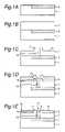
- FIGS, 1 A, 1 B, 1 C, 1 D and 1 Eare views for explaining a semiconductor device fabricating method according to a first embodiment of the present invention
- FIGS. 2A , 2 B and 2 Care views for explaining an etching process of the first embodiment
- FIG. 3is a view for explaining a state immediately before the execution of the solid state bonding of the first embodiment
- FIG. 4is a sectional view of the semiconductor device of the first embodiment
- FIGS. 5A , 5 B, 5 C, 5 D and 5 Eare views for explaining a semiconductor device fabricating method according to a second embodiment of the present invention.
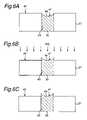
- FIGS. 6A , 6 B and 6 Care views for explaining an etching process of the second embodiment
- FIG. 7is a view for explaining a state immediately before the execution of the solid state bonding of the second embodiment.
- FIG. 8is a sectional view of the semiconductor device of the second embodiment.
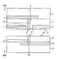
- FIGS. 1A through 1E , 2 A through 2 C, 3 and 4show a semiconductor device fabricating method of the first embodiment.
- a wiring layer 3is provided as an example of a conductive layer on a semiconductor substrate 1 that serves as an example of a first substrate.
- an insulating layer 7is laminated on the semiconductor substrate 1 and the wiring layer 3 .
- the wiring layer 3is made of a metal of, for example, copper, an aluminum alloy or the like, a polysilicon doped with an impurity, a silicide or the like, while the insulating layer 7 is made of, for example, silicon nitride.
- a through hole 13 that reaches the wiring layer 3is formed through the insulating layer 7 , and a grounding wiring groove 8 is formed on the insulating layer 7 by the techniques of photolithography and dry etching.
- a portion of the insulating layer 7 that is left between the through hole 13 and the grounding wiring groove 8becomes a through hole insulator 11 that forms a wall surface of the through hole 13 .
- a conductive layer 9 made of, for example, copperis formed on the insulating layer 7 so as to entirely cover the insulating layer 7 and fill up the through hole 13 and the grounding wiring groove 8 .
- the conductive layer 9is flattened by polishing according to the CMP method until the through hole insulator 11 is exposed. As described above, by performing polishing according to the CMP method until the through hole insulator 11 is exposed, the conductive layer 9 is separated into a through hole conductor 5 that is made of copper and fills up the through hole 13 and a grounding wiring layer 6 that buries the grounding wiring groove 8 . The surfaces of the through hole conductor 5 , the through hole insulator 11 and the grounding wiring layer 6 form a bonding surface 12 of an approximately same height.
- the through hole conductor 5 and the grounding wiring layer 6which are made of copper, have a hardness lower than that of the through hole insulator 11 . Therefore, as shown in FIG. 1E and FIG. 2A , the surfaces of the through hole conductor 5 and the grounding wiring layer 6 become concave in a dish-like shape and lowered with respect to the surface of the through hole insulator 11 by the CMP. That is, a dishing portion 17 that is concave in a dish-like shape occurs on the surface of the through hole conductor 5 .
- the through hole insulator 11is selectively etched until the through hole insulator 11 comes to have a height equal to the height of the bottom portion 19 of the dishing portion 17 of the through hole conductor 5 .
- This reactive ion etchinghas selectivity and anisotropy, and therefore, the through hole insulator 11 can be finely processed to make the through hole insulator 11 have a height approximately equal to the height of the bottom portion 19 of the dishing portion 17 .
- the height of the surface of the through hole insulator 11is lowered with respect to the height of the surface of the through hole conductor 5 . That is, the through hole conductor 5 is protruding from the surface of the through hole insulator 11 .
- a first portion 100 constructed of the semiconductor substrate 1 , the wiring layer 3 , the insulating layer 7 , the through hole insulator 11 , the through hole conductor 5 and the grounding wiring layer 6is thus formed.
- semiconductor elementssuch as transistors, capacitors and so on are built in the first portion 100 .
- a second portion 200 as shown in FIG. 3is formed.
- This second portion 200is constructed of a semiconductor substrate 20 that serves as a second substrate, a wiring layer 23 that serves as a conductive layer, an insulating layer 27 , a grounding wiring layer 26 that serves as a conductive layer, a through hole insulator 21 and a through hole conductor 25 .
- a bonding surface 22 of this second portion 200is flattened by polishing according to the CMP method, and therefore, a dishing portion is formed on the through hole conductor 25 and the grounding wiring layer 26 , which serve as conductive regions.
- the through hole insulator 21is selectively etched by reactive ion etching so that the bottom portion of the dishing portion 29 of the through hole conductor 25 and the through hole insulator 21 come to have an approximately equal height.
- a reference numeral 28denotes a through hole.
- semiconductor elementssuch as transistors, capacitors and so on are built in the second portion 200 , similarly to the first portion.
- the bonding surfaces 12 and 22 of the first portion 100 and the second portion 200are subjected to a cleaning process in a vacuum to become clean surfaces.
- the bonding surfaces 12 and 22are activated.
- the bonding surface 12 of the first portion 100 and the bonding surface 22 of the second portion 200are made to face each other in a manner that the through hole conductors 5 and 25 are aligned with each other and the grounding wiring layers 6 and 26 are aligned with each other, respectively. Then, as shown in FIG.
- the through hole conductors 5 and 25are solid-state-bonded or bonded at a room temperature (room temperature bonding) to each other, and the grounding wiring layers 6 and 26 are solid-state-bonded to each other. Then, the height of the bottom portions of the dishing portions 17 and 29 of the through hole conductors 5 and 25 becomes approximately equal to the height of the through hole insulators 11 and 21 . As a whole, the through hole conductors 5 and 25 and the grounding wiring layers 6 and 26 are convex with respect to the surfaces of the through hole insulators 11 and 21 .
- the through hole conductor 5 and the grounding wiring layer 6are securely solid-state-bonded to the through hole conductor 25 and the grounding wiring layer 26 , respectively.
- the electrical connection of the through hole conductors 5 and 25 and the electrical connection of the grounding wiring layers 6 and 26can be improved in terms of reliability.
- a clearance 30occurs in a portion located between the through hole insulators 11 and 21 and around the through hole conductors 5 and 25 that have been solid-state-bonded (i.e., in a surface activated bonding manner).
- the through hole conductors 5 and 25 and the grounding wiring layers 6 and 26can be more securely solid-state-bonded to each other, respectively, enabling the achievement of more secure mechanical and electrical bonding. It is also acceptable to put the through hole insulators 11 and 21 in light contact or make them solid-state-bonded without providing the clearance 30 .
- the bonding of the first portion 100 to the second portion 200is made more firm.
- the surfaces of the through hole insulators 11 and 21are lowered with respect to the surfaces of the through hole conductors 5 and 25 on both the bonding surface 12 of the first portion 100 and the bonding surface 22 of the second portion 200 .
- it is acceptable to perform etchingso that the through hole insulator is much lowered with respect to the surface of the through hole conductor on one bonding surface and to make the entire surface of the dishing portion of the through hole conductor lower than the surface of the through hole insulator without performing the etching for adjusting the height of the through hole insulator on the other bonding surface.
- Even with this arrangementby increasing the quantity of etching of one through hole insulator, the through hole conductors can be securely electrically connected to each other even through the dishing portions exist.
- FIGS. 5A through 5E , 6 A through 6 C, 7 and 8are views for explaining the semiconductor device fabricating method of the second embodiment.
- a first portion 100has the same construction as that of the first portion 100 of the first embodiment and is fabricated through the same processes. Therefore, no description is provided for the first portion 100 , and the same reference numerals as those used in the first embodiment are used.
- a second portion 300is fabricated through the processes shown in FIGS. 5A through 5E and 6 A through 6 C.
- a wiring layer 33is provided as an example of the conductive layer on a semiconductor substrate 31 that serves as an example of the second substrate.
- an insulating layer 37is laminated on the semiconductor substrate 31 and the wiring layer 33 .
- the wiring layer 33is made of a polysilicon doped with an impurity, copper, an aluminum alloy or the like, while the insulating layer 37 is made of, for example, silicon nitride, silicon oxide or the like.
- a through hole 43 that reaches the wiring layer 33is formed through the insulating layer 37 by the techniques of photolithography and dry etching.
- a conductive layer 39 made of, for example, polysiliconis formed on the insulator 37 and the wiring layer 33 located at the bottom of the through hole 43 so as to fill up the through hole 43 .
- the conductive layer 39 and the insulating layer 37are flattened by polishing according to the CMP method.
- the surfaces of the through hole conductor 35 positioned inside the through hole 43 and the insulating layer 37form a bonding surface 42 having an approximately equal height.
- the through hole conductor 35 made of polysiliconhas a hardness lower than that of the insulating layer 37 made of silicon nitride. Therefore, as shown in FIG. 5E and FIG. 6A , the surface of the through hole conductor 35 becomes concave in a dish-like shape and lowered with respect to the surface of the insulating layer 37 by the CMP. That is, a dishing portion 47 that is concave in a dish-like shape occurs on the surface of the through hole conductor 35 .
- the insulating layer 37is selectively etched until the insulating layer 37 comes to have a height equal to the height of the bottom portion 49 of the dishing portion 47 of the through hole conductor 35 .
- the height of the surface of the insulating layer 37is lowered with respect to the height of the surface of the through hole conductor 35 . That is, the through hole conductor 35 is protruding from the surface of the insulating layer 37 .
- the second portion 300 constructed of the semiconductor substrate 31 , the wiring layer 33 , the insulating layer 37 and the through hole conductor 35is thus formed.
- the bonding surfaces 12 and 42 of the first portion 100 and the second portion 300are subjected to a cleaning process in a vacuum to become clean surfaces.
- the bonding surfaces 12 and 42are activated.
- the bonding surface 12 of the first portion 100 and the bonding surface 42 of the second portion 300are made to face each other in a manner that the through hole conductors 5 and 35 are aligned with each other. Then, as shown in FIG.
- the through hole conductors 5 and 35are solid-state-bonded to each other, and the grounding wiring layer 6 and the insulating layer 37 are solid-state-bonded to each other. Then, the height of the bottom portion of the dishing portion 17 of the through hole conductor 5 becomes approximately equal to the height of the through hole insulator 11 .
- the through hole conductor 5 and the grounding wiring layer 6are totally convex with respect to the through hole insulator 11 .
- the height of the bottom portion of the dishing portion 47 of the through hole conductor 35is approximately equal to the height of the insulating layer 37 , and the through hole conductor 35 is convex with respect to the insulating layer 37 . Therefore, the through hole conductor 5 and the through hole conductor 35 are securely solid-state-bonded to each other, while the grounding wiring layer 6 and the insulating layer 37 are securely solid-state-bonded to each other. With this arrangement, the mechanical connection and electrical connection of the through hole conductors 5 and 35 as well as the mechanical connection of the grounding wiring layer 6 and the insulating layer 37 can be improved in terms of reliability.
- a clearance 40occurs between the through hole insulator 11 and the insulating layer 37 and around the through hole conductors 5 and 35 that have been solid-state-bonded.
- the clearance 40between the through hole insulator 11 and the insulating layer 37 , the solid state bonding of the through hole conductor 5 to the through hole conductor 35 and the solid state bonding of the grounding wiring layer 6 to the insulating layer 37 can be further secured for the achievement of more secure mechanical and electrical bonding. It is also acceptable to put the through hole insulator 11 and the insulating layer 37 in light contact or make them solid-state-bonded without providing, the clearance 40 . As described above, when the through hole insulator 11 and the insulating layer 37 are solid-state-bonded to each other, the bonding of the first portion 100 to the second portion 300 is made more firm.
- the insulating regions (through hole insulators and insulating layer) 11 , 21 and 37surround the conductive regions (through hole conductors) 5 , 25 and 35 on the bonding surfaces 12 , 22 and 42 .
- the insulating regionsare not required to surround the respective conductive regions, and it is only required to provide the conductive regions and the insulating regions. It is also acceptable that one bonding surface has the conductive region and the insulating region while the other bonding surface has only the conductive region.
- the insulating regionis etched so that the dishing portion in the conductive region protrudes above the insulating region on the bonding surface polished by the CMP method. Therefore, the present invention can be applicable if at least one bonding surface has the conductive region and the insulating region.
- the through hole conductor 5is solid-state-bonded to the through hole conductor 25 or 35
- the grounding wiring layer 6is solid-state-bonded to the grounding wiring layer 26 or the insulating layer 37 .
- the present inventionis, of course, not limited to this.
- the conductive layeris made of copper or polysilicon in the aforementioned embodiments, the conductive layer may be formed of, for example, silicide, an aluminum alloy or the like, while the insulating layer may be formed of silicon oxide besides the silicon nitride.
- the semiconductor substrateis employed as a substrate in the aforementioned embodiments, it is acceptable to employ an inorganic substrate such as a glass substrate and a ceramic substrate or an organic substrate made of an organic compound.
- the insulating regionis lowered with respect to the conductive region on at least one of the two bonding surfaces that are to be polished by the CMP method and then solid-state-bonded. Therefore, the conductive regions can be securely subjected to solid state bonding and securely electrically connected to each other.
- the insulating regionis selectively etched so that the surface of the insulating region is lowered with respect to the surface of the conductive region on at least one of the two bonding surfaces that have been polished by the CMP method. Therefore, the conductive regions can be securely subjected to solid state bonding and securely electrically connected to each other even though a dishing portion exists on the conductive region.
Landscapes
- Engineering & Computer Science (AREA)
- Microelectronics & Electronic Packaging (AREA)
- Power Engineering (AREA)
- Computer Hardware Design (AREA)
- Physics & Mathematics (AREA)
- Condensed Matter Physics & Semiconductors (AREA)
- General Physics & Mathematics (AREA)
- Manufacturing & Machinery (AREA)
- Internal Circuitry In Semiconductor Integrated Circuit Devices (AREA)
Abstract
Description
Claims (18)
Priority Applications (1)
| Application Number | Priority Date | Filing Date | Title |
|---|---|---|---|
| US11/077,212US7217631B2 (en) | 2000-07-05 | 2005-03-11 | Semiconductor device and method for fabricating the device |
Applications Claiming Priority (4)
| Application Number | Priority Date | Filing Date | Title |
|---|---|---|---|
| JP2000-203871 | 2000-07-05 | ||
| JP2000203871AJP3440057B2 (en) | 2000-07-05 | 2000-07-05 | Semiconductor device and manufacturing method thereof |
| US09/898,082US7078811B2 (en) | 2000-07-05 | 2001-07-05 | Semiconductor device and method for fabricating the device |
| US11/077,212US7217631B2 (en) | 2000-07-05 | 2005-03-11 | Semiconductor device and method for fabricating the device |
Related Parent Applications (1)
| Application Number | Title | Priority Date | Filing Date |
|---|---|---|---|
| US09/898,082DivisionUS7078811B2 (en) | 2000-07-05 | 2001-07-05 | Semiconductor device and method for fabricating the device |
Publications (2)
| Publication Number | Publication Date |
|---|---|
| US20050170626A1 US20050170626A1 (en) | 2005-08-04 |
| US7217631B2true US7217631B2 (en) | 2007-05-15 |
Family
ID=18701224
Family Applications (2)
| Application Number | Title | Priority Date | Filing Date |
|---|---|---|---|
| US09/898,082Expired - LifetimeUS7078811B2 (en) | 2000-07-05 | 2001-07-05 | Semiconductor device and method for fabricating the device |
| US11/077,212Expired - LifetimeUS7217631B2 (en) | 2000-07-05 | 2005-03-11 | Semiconductor device and method for fabricating the device |
Family Applications Before (1)
| Application Number | Title | Priority Date | Filing Date |
|---|---|---|---|
| US09/898,082Expired - LifetimeUS7078811B2 (en) | 2000-07-05 | 2001-07-05 | Semiconductor device and method for fabricating the device |
Country Status (5)
| Country | Link |
|---|---|
| US (2) | US7078811B2 (en) |
| JP (1) | JP3440057B2 (en) |
| KR (1) | KR100438163B1 (en) |
| DE (1) | DE10132024B4 (en) |
| TW (1) | TW495958B (en) |
Cited By (9)
| Publication number | Priority date | Publication date | Assignee | Title |
|---|---|---|---|---|
| US20080237310A1 (en)* | 2007-03-26 | 2008-10-02 | Shanggar Periaman | Die backside wire bond technology for single or stacked die package |
| US20090065951A1 (en)* | 2007-09-10 | 2009-03-12 | Bok Eng Cheah | Stacked die package |
| US20150028493A1 (en)* | 2013-07-23 | 2015-01-29 | Kabushiki Kaisha Toshiba | Semiconductor device and manufacturing method thereof |
| US20150162294A1 (en)* | 2013-12-11 | 2015-06-11 | Kabushiki Kaisha Toshiba | Method for manufacturing semiconductor device and semiconductor device |
| US10381322B1 (en) | 2018-04-23 | 2019-08-13 | Sandisk Technologies Llc | Three-dimensional memory device containing self-aligned interlocking bonded structure and method of making the same |
| US10879260B2 (en) | 2019-02-28 | 2020-12-29 | Sandisk Technologies Llc | Bonded assembly of a support die and plural memory dies containing laterally shifted vertical interconnections and methods for making the same |
| US20220093492A1 (en)* | 2020-09-18 | 2022-03-24 | Intel Corporation | Direct bonding in microelectronic assemblies |
| US11990448B2 (en) | 2020-09-18 | 2024-05-21 | Intel Corporation | Direct bonding in microelectronic assemblies |
| US12381168B2 (en) | 2015-08-25 | 2025-08-05 | Adeia Semiconductor Bonding Technologies Inc. | Conductive barrier direct hybrid bonding |
Families Citing this family (108)
| Publication number | Priority date | Publication date | Assignee | Title |
|---|---|---|---|---|
| FR2773261B1 (en) | 1997-12-30 | 2000-01-28 | Commissariat Energie Atomique | METHOD FOR THE TRANSFER OF A THIN FILM COMPRISING A STEP OF CREATING INCLUSIONS |
| JP2002353424A (en)* | 2001-03-23 | 2002-12-06 | Seiko Epson Corp | Method for manufacturing substrate device and substrate device, method for manufacturing electro-optical device, electro-optical device, and electronic apparatus |
| US6793759B2 (en) | 2001-10-09 | 2004-09-21 | Dow Corning Corporation | Method for creating adhesion during fabrication of electronic devices |
| US6596640B1 (en)* | 2002-06-21 | 2003-07-22 | Intel Corporation | Method of forming a raised contact for a substrate |
| US7064055B2 (en)* | 2002-12-31 | 2006-06-20 | Massachusetts Institute Of Technology | Method of forming a multi-layer semiconductor structure having a seamless bonding interface |
| AU2003300040A1 (en)* | 2002-12-31 | 2004-07-29 | Massachusetts Institute Of Technology | Multi-layer integrated semiconductor structure having an electrical shielding portion |
| US20040124538A1 (en)* | 2002-12-31 | 2004-07-01 | Rafael Reif | Multi-layer integrated semiconductor structure |
| US6962835B2 (en) | 2003-02-07 | 2005-11-08 | Ziptronix, Inc. | Method for room temperature metal direct bonding |
| FR2856844B1 (en)* | 2003-06-24 | 2006-02-17 | Commissariat Energie Atomique | HIGH PERFORMANCE CHIP INTEGRATED CIRCUIT |
| FR2861497B1 (en) | 2003-10-28 | 2006-02-10 | Soitec Silicon On Insulator | METHOD FOR CATASTROPHIC TRANSFER OF A FINE LAYER AFTER CO-IMPLANTATION |
| US7602069B2 (en) | 2004-03-31 | 2009-10-13 | Universität Duisburg-Essen | Micro electronic component with electrically accessible metallic clusters |
| US20050218394A1 (en)* | 2004-03-31 | 2005-10-06 | Gunther Schmid | Micro electronic component |
| US7485968B2 (en) | 2005-08-11 | 2009-02-03 | Ziptronix, Inc. | 3D IC method and device |
| US8241995B2 (en)* | 2006-09-18 | 2012-08-14 | International Business Machines Corporation | Bonding of substrates including metal-dielectric patterns with metal raised above dielectric |
| FR2910179B1 (en) | 2006-12-19 | 2009-03-13 | Commissariat Energie Atomique | METHOD FOR MANUFACTURING THIN LAYERS OF GaN BY IMPLANTATION AND RECYCLING OF A STARTING SUBSTRATE |
| FR2910706B1 (en)* | 2006-12-21 | 2009-03-20 | Commissariat Energie Atomique | INTERCONNECTION ELEMENT BASED ON CARBON NANOTUBES |
| FR2913145B1 (en) | 2007-02-22 | 2009-05-15 | Stmicroelectronics Crolles Sas | ASSEMBLY OF TWO PARTS OF INTEGRATED ELECTRONIC CIRCUIT |
| US8134235B2 (en)* | 2007-04-23 | 2012-03-13 | Taiwan Semiconductor Manufacturing Co., Ltd. | Three-dimensional semiconductor device |
| US8350382B2 (en)* | 2007-09-21 | 2013-01-08 | Infineon Technologies Ag | Semiconductor device including electronic component coupled to a backside of a chip |
| US7999388B2 (en)* | 2007-09-24 | 2011-08-16 | Research Triangle Institute | Preventing breakage of long metal signal conductors on semiconductor substrates |
| US8053900B2 (en)* | 2008-10-21 | 2011-11-08 | Taiwan Semiconductor Manufacturing Company, Ltd. | Through-substrate vias (TSVs) electrically connected to a bond pad design with reduced dishing effect |
| FR2947098A1 (en) | 2009-06-18 | 2010-12-24 | Commissariat Energie Atomique | METHOD OF TRANSFERRING A THIN LAYER TO A TARGET SUBSTRATE HAVING A THERMAL EXPANSION COEFFICIENT DIFFERENT FROM THAT OF THE THIN LAYER |
| JP5272922B2 (en)* | 2009-06-24 | 2013-08-28 | 日本電気株式会社 | Semiconductor device and manufacturing method thereof |
| FI123860B (en)* | 2010-05-18 | 2013-11-29 | Corelase Oy | Method for sealing and contacting substrates with laser light |
| JP6342033B2 (en)* | 2010-06-30 | 2018-06-13 | キヤノン株式会社 | Solid-state imaging device |
| JP2012033894A (en) | 2010-06-30 | 2012-02-16 | Canon Inc | Solid state image sensor |
| TWI422009B (en)* | 2010-07-08 | 2014-01-01 | Nat Univ Tsing Hua | Multi-chip stacked structure |
| JP5517800B2 (en) | 2010-07-09 | 2014-06-11 | キヤノン株式会社 | Member for solid-state imaging device and method for manufacturing solid-state imaging device |
| EP2717300B1 (en) | 2011-05-24 | 2020-03-18 | Sony Corporation | Semiconductor device |
| JP6291822B2 (en)* | 2012-12-25 | 2018-03-14 | 株式会社ニコン | Substrate and substrate bonding method |
| WO2015040784A1 (en)* | 2013-09-17 | 2015-03-26 | パナソニックIpマネジメント株式会社 | Semiconductor device and method for manufacturing same |
| US20150262902A1 (en) | 2014-03-12 | 2015-09-17 | Invensas Corporation | Integrated circuits protected by substrates with cavities, and methods of manufacture |
| TWI517343B (en)* | 2014-03-25 | 2016-01-11 | 恆勁科技股份有限公司 | Flip-chip package-on-package structure and its fabrication method |
| US11069734B2 (en) | 2014-12-11 | 2021-07-20 | Invensas Corporation | Image sensor device |
| JP6165127B2 (en) | 2014-12-22 | 2017-07-19 | 三菱重工工作機械株式会社 | Semiconductor device and manufacturing method of semiconductor device |
| US9741620B2 (en) | 2015-06-24 | 2017-08-22 | Invensas Corporation | Structures and methods for reliable packages |
| CN104979226B (en)* | 2015-06-24 | 2018-09-07 | 武汉新芯集成电路制造有限公司 | A kind of hybrid bonded method of copper |
| US10886250B2 (en) | 2015-07-10 | 2021-01-05 | Invensas Corporation | Structures and methods for low temperature bonding using nanoparticles |
| US9852988B2 (en) | 2015-12-18 | 2017-12-26 | Invensas Bonding Technologies, Inc. | Increased contact alignment tolerance for direct bonding |
| US10446532B2 (en) | 2016-01-13 | 2019-10-15 | Invensas Bonding Technologies, Inc. | Systems and methods for efficient transfer of semiconductor elements |
| US10204893B2 (en) | 2016-05-19 | 2019-02-12 | Invensas Bonding Technologies, Inc. | Stacked dies and methods for forming bonded structures |
| JP6865544B2 (en)* | 2016-07-27 | 2021-04-28 | 日本放送協会 | Spatial Light Modulators and Methods for Manufacturing Spatial Light Modulators |
| US10446487B2 (en) | 2016-09-30 | 2019-10-15 | Invensas Bonding Technologies, Inc. | Interface structures and methods for forming same |
| US10580735B2 (en) | 2016-10-07 | 2020-03-03 | Xcelsis Corporation | Stacked IC structure with system level wiring on multiple sides of the IC die |
| TWI822659B (en) | 2016-10-27 | 2023-11-21 | 美商艾德亞半導體科技有限責任公司 | Structures and methods for low temperature bonding |
| US10002844B1 (en) | 2016-12-21 | 2018-06-19 | Invensas Bonding Technologies, Inc. | Bonded structures |
| US20180182665A1 (en) | 2016-12-28 | 2018-06-28 | Invensas Bonding Technologies, Inc. | Processed Substrate |
| CN117878055A (en) | 2016-12-28 | 2024-04-12 | 艾德亚半导体接合科技有限公司 | Stacking substrate processing |
| TWI837879B (en) | 2016-12-29 | 2024-04-01 | 美商艾德亞半導體接合科技有限公司 | Bonded structures with integrated passive component |
| US10276909B2 (en) | 2016-12-30 | 2019-04-30 | Invensas Bonding Technologies, Inc. | Structure comprising at least a first element bonded to a carrier having a closed metallic channel waveguide formed therein |
| EP3580166A4 (en) | 2017-02-09 | 2020-09-02 | Invensas Bonding Technologies, Inc. | Bonded structures |
| WO2018169968A1 (en) | 2017-03-16 | 2018-09-20 | Invensas Corporation | Direct-bonded led arrays and applications |
| US10515913B2 (en) | 2017-03-17 | 2019-12-24 | Invensas Bonding Technologies, Inc. | Multi-metal contact structure |
| US10508030B2 (en) | 2017-03-21 | 2019-12-17 | Invensas Bonding Technologies, Inc. | Seal for microelectronic assembly |
| US10784191B2 (en) | 2017-03-31 | 2020-09-22 | Invensas Bonding Technologies, Inc. | Interface structures and methods for forming same |
| US10269756B2 (en) | 2017-04-21 | 2019-04-23 | Invensas Bonding Technologies, Inc. | Die processing |
| US10879212B2 (en) | 2017-05-11 | 2020-12-29 | Invensas Bonding Technologies, Inc. | Processed stacked dies |
| US10446441B2 (en) | 2017-06-05 | 2019-10-15 | Invensas Corporation | Flat metal features for microelectronics applications |
| US10217720B2 (en) | 2017-06-15 | 2019-02-26 | Invensas Corporation | Multi-chip modules formed using wafer-level processing of a reconstitute wafer |
| US10840205B2 (en) | 2017-09-24 | 2020-11-17 | Invensas Bonding Technologies, Inc. | Chemical mechanical polishing for hybrid bonding |
| US10923408B2 (en) | 2017-12-22 | 2021-02-16 | Invensas Bonding Technologies, Inc. | Cavity packages |
| US11380597B2 (en) | 2017-12-22 | 2022-07-05 | Invensas Bonding Technologies, Inc. | Bonded structures |
| US10727219B2 (en) | 2018-02-15 | 2020-07-28 | Invensas Bonding Technologies, Inc. | Techniques for processing devices |
| US11169326B2 (en) | 2018-02-26 | 2021-11-09 | Invensas Bonding Technologies, Inc. | Integrated optical waveguides, direct-bonded waveguide interface joints, optical routing and interconnects |
| US11256004B2 (en) | 2018-03-20 | 2022-02-22 | Invensas Bonding Technologies, Inc. | Direct-bonded lamination for improved image clarity in optical devices |
| US11056348B2 (en) | 2018-04-05 | 2021-07-06 | Invensas Bonding Technologies, Inc. | Bonding surfaces for microelectronics |
| US10790262B2 (en) | 2018-04-11 | 2020-09-29 | Invensas Bonding Technologies, Inc. | Low temperature bonded structures |
| US11244916B2 (en) | 2018-04-11 | 2022-02-08 | Invensas Bonding Technologies, Inc. | Low temperature bonded structures |
| US10964664B2 (en) | 2018-04-20 | 2021-03-30 | Invensas Bonding Technologies, Inc. | DBI to Si bonding for simplified handle wafer |
| JP7258494B2 (en)* | 2018-04-26 | 2023-04-17 | 株式会社Maruwa | COMPOSITE SUBSTRATE AND METHOD FOR MANUFACTURING COMPOSITE SUBSTRATE |
| US11004757B2 (en) | 2018-05-14 | 2021-05-11 | Invensas Bonding Technologies, Inc. | Bonded structures |
| US11276676B2 (en) | 2018-05-15 | 2022-03-15 | Invensas Bonding Technologies, Inc. | Stacked devices and methods of fabrication |
| US11393779B2 (en) | 2018-06-13 | 2022-07-19 | Invensas Bonding Technologies, Inc. | Large metal pads over TSV |
| KR20210009426A (en) | 2018-06-13 | 2021-01-26 | 인벤사스 본딩 테크놀로지스 인코포레이티드 | TV as a pad |
| US11462419B2 (en) | 2018-07-06 | 2022-10-04 | Invensas Bonding Technologies, Inc. | Microelectronic assemblies |
| US11158606B2 (en) | 2018-07-06 | 2021-10-26 | Invensas Bonding Technologies, Inc. | Molded direct bonded and interconnected stack |
| US12406959B2 (en) | 2018-07-26 | 2025-09-02 | Adeia Semiconductor Bonding Technologies Inc. | Post CMP processing for hybrid bonding |
| US11515291B2 (en) | 2018-08-28 | 2022-11-29 | Adeia Semiconductor Inc. | Integrated voltage regulator and passive components |
| US20200075533A1 (en) | 2018-08-29 | 2020-03-05 | Invensas Bonding Technologies, Inc. | Bond enhancement in microelectronics by trapping contaminants and arresting cracks during direct-bonding processes |
| US11011494B2 (en) | 2018-08-31 | 2021-05-18 | Invensas Bonding Technologies, Inc. | Layer structures for making direct metal-to-metal bonds at low temperatures in microelectronics |
| CN109119426B (en)* | 2018-09-28 | 2024-04-16 | 长江存储科技有限责任公司 | 3D memory device |
| US11158573B2 (en) | 2018-10-22 | 2021-10-26 | Invensas Bonding Technologies, Inc. | Interconnect structures |
| CN109390305B (en)* | 2018-10-22 | 2021-05-11 | 长江存储科技有限责任公司 | Bonding wafer and preparation method thereof |
| US11244920B2 (en) | 2018-12-18 | 2022-02-08 | Invensas Bonding Technologies, Inc. | Method and structures for low temperature device bonding |
| CN113330557A (en) | 2019-01-14 | 2021-08-31 | 伊文萨思粘合技术公司 | Bonding structure |
| US11901281B2 (en) | 2019-03-11 | 2024-02-13 | Adeia Semiconductor Bonding Technologies Inc. | Bonded structures with integrated passive component |
| US11610846B2 (en) | 2019-04-12 | 2023-03-21 | Adeia Semiconductor Bonding Technologies Inc. | Protective elements for bonded structures including an obstructive element |
| US11205625B2 (en) | 2019-04-12 | 2021-12-21 | Invensas Bonding Technologies, Inc. | Wafer-level bonding of obstructive elements |
| US11373963B2 (en) | 2019-04-12 | 2022-06-28 | Invensas Bonding Technologies, Inc. | Protective elements for bonded structures |
| US11355404B2 (en) | 2019-04-22 | 2022-06-07 | Invensas Bonding Technologies, Inc. | Mitigating surface damage of probe pads in preparation for direct bonding of a substrate |
| US11385278B2 (en) | 2019-05-23 | 2022-07-12 | Invensas Bonding Technologies, Inc. | Security circuitry for bonded structures |
| US12374641B2 (en) | 2019-06-12 | 2025-07-29 | Adeia Semiconductor Bonding Technologies Inc. | Sealed bonded structures and methods for forming the same |
| US11315871B2 (en) | 2019-06-13 | 2022-04-26 | Nanya Technology Corporation | Integrated circuit device with bonding structure and method of forming the same |
| US11296053B2 (en) | 2019-06-26 | 2022-04-05 | Invensas Bonding Technologies, Inc. | Direct bonded stack structures for increased reliability and improved yield in microelectronics |
| US12080672B2 (en) | 2019-09-26 | 2024-09-03 | Adeia Semiconductor Bonding Technologies Inc. | Direct gang bonding methods including directly bonding first element to second element to form bonded structure without adhesive |
| US11762200B2 (en) | 2019-12-17 | 2023-09-19 | Adeia Semiconductor Bonding Technologies Inc. | Bonded optical devices |
| CN112885777B (en) | 2020-01-07 | 2022-12-09 | 长江存储科技有限责任公司 | Metal-dielectric bonding method and structure |
| US11742314B2 (en) | 2020-03-31 | 2023-08-29 | Adeia Semiconductor Bonding Technologies Inc. | Reliable hybrid bonded apparatus |
| WO2021236361A1 (en) | 2020-05-19 | 2021-11-25 | Invensas Bonding Technologies, Inc. | Laterally unconfined structure |
| US11631647B2 (en) | 2020-06-30 | 2023-04-18 | Adeia Semiconductor Bonding Technologies Inc. | Integrated device packages with integrated device die and dummy element |
| KR102712153B1 (en) | 2020-07-29 | 2024-09-30 | 삼성전자주식회사 | semiconductor package for improving the bonding reliability |
| US11728273B2 (en) | 2020-09-04 | 2023-08-15 | Adeia Semiconductor Bonding Technologies Inc. | Bonded structure with interconnect structure |
| US11764177B2 (en) | 2020-09-04 | 2023-09-19 | Adeia Semiconductor Bonding Technologies Inc. | Bonded structure with interconnect structure |
| US11264357B1 (en) | 2020-10-20 | 2022-03-01 | Invensas Corporation | Mixed exposure for large die |
| JP2022096892A (en)* | 2020-12-18 | 2022-06-30 | ソニーセミコンダクタソリューションズ株式会社 | Semiconductor devices, semiconductor device manufacturing methods, and electronic devices |
| JP2024501017A (en) | 2020-12-28 | 2024-01-10 | アデイア セミコンダクター ボンディング テクノロジーズ インコーポレイテッド | Structure with through-substrate via and method for forming the same |
| JP2024501559A (en) | 2020-12-30 | 2024-01-12 | アデイア セミコンダクター ボンディング テクノロジーズ インコーポレイテッド | Structures with conductive features and methods of forming the same |
| KR20240036698A (en) | 2021-08-02 | 2024-03-20 | 아데이아 세미컨덕터 본딩 테크놀로지스 인코포레이티드 | Protective semiconductor elements for combined structures |
Citations (14)
| Publication number | Priority date | Publication date | Assignee | Title |
|---|---|---|---|---|
| US4612083A (en) | 1984-07-20 | 1986-09-16 | Nec Corporation | Process of fabricating three-dimensional semiconductor device |
| WO1989003122A1 (en) | 1987-09-24 | 1989-04-06 | Santa Barbara Research Center | Oxide removal from metallic contact bumps formed on semiconductor devices to improve hybridization cold-welds |
| US4939568A (en) | 1986-03-20 | 1990-07-03 | Fujitsu Limited | Three-dimensional integrated circuit and manufacturing method thereof |
| EP0700088A2 (en) | 1994-08-29 | 1996-03-06 | Matsushita Electric Industrial Co., Ltd. | Semiconductor device and comprising two semiconductor substrates |
| US5939789A (en) | 1994-02-28 | 1999-08-17 | Hitachi, Ltd. | Multilayer substrates methods for manufacturing multilayer substrates and electronic devices |
| JPH11284066A (en) | 1998-03-26 | 1999-10-15 | Ricoh Co Ltd | Semiconductor device and manufacturing method thereof |
| US5986339A (en) | 1997-02-13 | 1999-11-16 | General Dynamics Information Systems, Inc. | Laminated multilayer substrates |
| US5985748A (en)* | 1997-12-01 | 1999-11-16 | Motorola, Inc. | Method of making a semiconductor device using chemical-mechanical polishing having a combination-step process |
| US6080640A (en) | 1997-07-11 | 2000-06-27 | Advanced Micro Devices, Inc. | Metal attachment method and structure for attaching substrates at low temperatures |
| US6171949B1 (en)* | 1999-06-09 | 2001-01-09 | Advanced Micro Devices, Inc. | Low energy passivation of conductive material in damascene process for semiconductors |
| US6251772B1 (en)* | 1999-04-29 | 2001-06-26 | Advanced Micro Devicees, Inc. | Dielectric adhesion enhancement in damascene process for semiconductors |
| US6255217B1 (en)* | 1999-01-04 | 2001-07-03 | International Business Machines Corporation | Plasma treatment to enhance inorganic dielectric adhesion to copper |
| US6281576B1 (en) | 1999-06-16 | 2001-08-28 | International Business Machines Corporation | Method of fabricating structure for chip micro-joining |
| US6541372B2 (en)* | 2000-03-07 | 2003-04-01 | Infineon Technologies Ag | Method for manufacturing a conductor structure for an integrated circuit |
Family Cites Families (7)
| Publication number | Priority date | Publication date | Assignee | Title |
|---|---|---|---|---|
| DE4314913C1 (en)* | 1993-05-05 | 1994-08-25 | Siemens Ag | Method for producing a semiconductor component with a contact structuring for vertical contacting with further semiconductor components |
| JPH09509011A (en)* | 1994-02-16 | 1997-09-09 | シーメンス アクチエンゲゼルシヤフト | Manufacturing method of three-dimensional circuit device |
| US5756395A (en)* | 1995-08-18 | 1998-05-26 | Lsi Logic Corporation | Process for forming metal interconnect structures for use with integrated circuit devices to form integrated circuit structures |
| JPH1083980A (en)* | 1996-09-06 | 1998-03-31 | Hitachi Ltd | Method for manufacturing semiconductor device |
| JPH10223636A (en)* | 1997-02-12 | 1998-08-21 | Nec Yamagata Ltd | Manufacture of semiconductor integrated circuit device |
| JP3532788B2 (en)* | 1999-04-13 | 2004-05-31 | 唯知 須賀 | Semiconductor device and manufacturing method thereof |
| WO2008093121A2 (en) | 2007-02-02 | 2008-08-07 | G24 Innovations Limited | Photovoltaic electrochemical cell arrays |
- 2000
- 2000-07-05JPJP2000203871Apatent/JP3440057B2/ennot_activeExpired - Lifetime
- 2001
- 2001-07-03DEDE10132024Apatent/DE10132024B4/ennot_activeExpired - Lifetime
- 2001-07-04KRKR10-2001-0039827Apatent/KR100438163B1/ennot_activeExpired - Lifetime
- 2001-07-05USUS09/898,082patent/US7078811B2/ennot_activeExpired - Lifetime
- 2001-07-05TWTW090116507Apatent/TW495958B/ennot_activeIP Right Cessation
- 2005
- 2005-03-11USUS11/077,212patent/US7217631B2/ennot_activeExpired - Lifetime
Patent Citations (14)
| Publication number | Priority date | Publication date | Assignee | Title |
|---|---|---|---|---|
| US4612083A (en) | 1984-07-20 | 1986-09-16 | Nec Corporation | Process of fabricating three-dimensional semiconductor device |
| US4939568A (en) | 1986-03-20 | 1990-07-03 | Fujitsu Limited | Three-dimensional integrated circuit and manufacturing method thereof |
| WO1989003122A1 (en) | 1987-09-24 | 1989-04-06 | Santa Barbara Research Center | Oxide removal from metallic contact bumps formed on semiconductor devices to improve hybridization cold-welds |
| US5939789A (en) | 1994-02-28 | 1999-08-17 | Hitachi, Ltd. | Multilayer substrates methods for manufacturing multilayer substrates and electronic devices |
| EP0700088A2 (en) | 1994-08-29 | 1996-03-06 | Matsushita Electric Industrial Co., Ltd. | Semiconductor device and comprising two semiconductor substrates |
| US5986339A (en) | 1997-02-13 | 1999-11-16 | General Dynamics Information Systems, Inc. | Laminated multilayer substrates |
| US6080640A (en) | 1997-07-11 | 2000-06-27 | Advanced Micro Devices, Inc. | Metal attachment method and structure for attaching substrates at low temperatures |
| US5985748A (en)* | 1997-12-01 | 1999-11-16 | Motorola, Inc. | Method of making a semiconductor device using chemical-mechanical polishing having a combination-step process |
| JPH11284066A (en) | 1998-03-26 | 1999-10-15 | Ricoh Co Ltd | Semiconductor device and manufacturing method thereof |
| US6255217B1 (en)* | 1999-01-04 | 2001-07-03 | International Business Machines Corporation | Plasma treatment to enhance inorganic dielectric adhesion to copper |
| US6251772B1 (en)* | 1999-04-29 | 2001-06-26 | Advanced Micro Devicees, Inc. | Dielectric adhesion enhancement in damascene process for semiconductors |
| US6171949B1 (en)* | 1999-06-09 | 2001-01-09 | Advanced Micro Devices, Inc. | Low energy passivation of conductive material in damascene process for semiconductors |
| US6281576B1 (en) | 1999-06-16 | 2001-08-28 | International Business Machines Corporation | Method of fabricating structure for chip micro-joining |
| US6541372B2 (en)* | 2000-03-07 | 2003-04-01 | Infineon Technologies Ag | Method for manufacturing a conductor structure for an integrated circuit |
Non-Patent Citations (3)
| Title |
|---|
| German Office Action dated Dec. 15, 2005 (w/English translation thereof). |
| U.S. Appl. No. 09/548,916, filed Apr. 13, 2000 entitled "Semiconductor Device and Manufacturing Method Thereof". |
| U.S. Appl. No. 09/898,082, filed Jul. 5, 2001. |
Cited By (18)
| Publication number | Priority date | Publication date | Assignee | Title |
|---|---|---|---|---|
| US20080237310A1 (en)* | 2007-03-26 | 2008-10-02 | Shanggar Periaman | Die backside wire bond technology for single or stacked die package |
| US8198716B2 (en) | 2007-03-26 | 2012-06-12 | Intel Corporation | Die backside wire bond technology for single or stacked die package |
| US20090065951A1 (en)* | 2007-09-10 | 2009-03-12 | Bok Eng Cheah | Stacked die package |
| US8044497B2 (en)* | 2007-09-10 | 2011-10-25 | Intel Corporation | Stacked die package |
| US20120003792A1 (en)* | 2007-09-10 | 2012-01-05 | Bok Eng Cheah | Stacked die package |
| US8697495B2 (en)* | 2007-09-10 | 2014-04-15 | Intel Corporation | Stacked die package |
| US9287225B2 (en)* | 2013-07-23 | 2016-03-15 | Kabushiki Kaisha Toshiba | Semiconductor device and manufacturing method thereof |
| US20150028493A1 (en)* | 2013-07-23 | 2015-01-29 | Kabushiki Kaisha Toshiba | Semiconductor device and manufacturing method thereof |
| US9673147B2 (en) | 2013-07-23 | 2017-06-06 | Kabushiki Kaisha Toshiba | Semiconductor device and manufacturing method thereof |
| US20150162294A1 (en)* | 2013-12-11 | 2015-06-11 | Kabushiki Kaisha Toshiba | Method for manufacturing semiconductor device and semiconductor device |
| US9437568B2 (en)* | 2013-12-11 | 2016-09-06 | Kabushiki Kaisha Toshiba | Method for manufacturing semiconductor device having a multilayer interconnection |
| US10840204B2 (en) | 2013-12-11 | 2020-11-17 | Toshiba Memory Corporation | Semiconductor device for bonding conductive layers exposed from surfaces of respective interconnection layers |
| US12381168B2 (en) | 2015-08-25 | 2025-08-05 | Adeia Semiconductor Bonding Technologies Inc. | Conductive barrier direct hybrid bonding |
| US10381322B1 (en) | 2018-04-23 | 2019-08-13 | Sandisk Technologies Llc | Three-dimensional memory device containing self-aligned interlocking bonded structure and method of making the same |
| US10879260B2 (en) | 2019-02-28 | 2020-12-29 | Sandisk Technologies Llc | Bonded assembly of a support die and plural memory dies containing laterally shifted vertical interconnections and methods for making the same |
| US20220093492A1 (en)* | 2020-09-18 | 2022-03-24 | Intel Corporation | Direct bonding in microelectronic assemblies |
| US11990448B2 (en) | 2020-09-18 | 2024-05-21 | Intel Corporation | Direct bonding in microelectronic assemblies |
| US12199018B2 (en)* | 2020-09-18 | 2025-01-14 | Intel Corporation | Direct bonding in microelectronic assemblies |
Also Published As
| Publication number | Publication date |
|---|---|
| DE10132024A1 (en) | 2002-01-24 |
| US20020003307A1 (en) | 2002-01-10 |
| JP3440057B2 (en) | 2003-08-25 |
| TW495958B (en) | 2002-07-21 |
| DE10132024B4 (en) | 2007-02-08 |
| JP2002026123A (en) | 2002-01-25 |
| US7078811B2 (en) | 2006-07-18 |
| US20050170626A1 (en) | 2005-08-04 |
| KR20020004874A (en) | 2002-01-16 |
| KR100438163B1 (en) | 2004-07-01 |
Similar Documents
| Publication | Publication Date | Title |
|---|---|---|
| US7217631B2 (en) | Semiconductor device and method for fabricating the device | |
| JP3354424B2 (en) | Semiconductor device and method of manufacturing semiconductor device | |
| KR100526445B1 (en) | Wafer passivation structure | |
| US6025277A (en) | Method and structure for preventing bonding pad peel back | |
| JP2012231173A (en) | Electrical connection between two surfaces of substrate and method of manufacturing the same | |
| KR100415045B1 (en) | Semiconductor device and method of manufacturing the same | |
| US6404058B1 (en) | Semiconductor device having interconnection implemented by refractory metal nitride layer and refractory metal silicide layer and process of fabrication thereof | |
| JPH1022457A (en) | Capacitance device, semiconductor device, and manufacturing method thereof | |
| US20040053427A1 (en) | Method of fabricating a ferromagnetic memory device | |
| US6576970B2 (en) | Bonding pad structure of semiconductor device and method for fabricating the same | |
| KR100294755B1 (en) | Semiconductor device and its manufacturing method | |
| US6211569B1 (en) | Interconnection lines for improving thermal conductivity in integrated circuits and method for fabricating the same | |
| JPH1197525A (en) | Semiconductor device and manufacturing method thereof | |
| CN112768462A (en) | Three-dimensional memory and preparation method thereof | |
| US20220189845A1 (en) | Heat dissipating substrate, manufacturing method thereof, and semiconductor integrated device including the same | |
| US7084057B2 (en) | Bit line contact structure and fabrication method thereof | |
| US7777342B2 (en) | Semiconductor device and method for manufacturing the same | |
| JP2003503854A (en) | Semiconductor device | |
| JPH09115888A (en) | Manufacture of semiconductor device | |
| KR100259168B1 (en) | Structure of metal interconnection line for semiconductor device and method of forming the same | |
| KR0172725B1 (en) | Multi-layer metal wire forming method of semiconductor device | |
| KR100457407B1 (en) | Method for forming metal interconnection of semiconductor device to improve electrical characteristic of metal interconnection | |
| US20020068437A1 (en) | Method of forming unlanded via | |
| KR100223872B1 (en) | Forming method of metalization structure | |
| KR20030058585A (en) | Method for manufacturing semiconductor device |
Legal Events
| Date | Code | Title | Description |
|---|---|---|---|
| AS | Assignment | Owner name:RENESAS TECHNOLOGY CORP., JAPAN Free format text:ASSIGNMENT OF ASSIGNORS INTEREST;ASSIGNOR:HITACHI, LTD.;REEL/FRAME:017927/0484 Effective date:20060315 Owner name:RENESAS TECHNOLOGY CORP., JAPAN Free format text:ASSIGNMENT OF ASSIGNORS INTEREST;ASSIGNORS:DENKI, MITSUBISHI;KAISHA, KABUSHIKI;REEL/FRAME:017927/0217 Effective date:20060315 | |
| AS | Assignment | Owner name:RENESAS TECHNOLOGY CORP., JAPAN Free format text:ASSIGNMENT OF ASSIGNORS INTEREST;ASSIGNORS:DENKI, MITSUBISHI;KAISHA, KABUSHIKI;REEL/FRAME:017950/0065 Effective date:20060315 | |
| AS | Assignment | Owner name:RENESAS TECHNOLOGY CORP., JAPAN Free format text:ASSIGNMENT OF ASSIGNORS INTEREST;ASSIGNOR:MITSUBISHI DENKI KABUSHIKI KAISHA;REEL/FRAME:017972/0602 Effective date:20060315 | |
| STCF | Information on status: patent grant | Free format text:PATENTED CASE | |
| AS | Assignment | Owner name:OKI SEMICONDUCTOR CO., LTD, JAPAN Free format text:CHANGE OF NAME;ASSIGNOR:OKI ELECTRIC INDUSTRY CO., LTD;REEL/FRAME:021901/0913 Effective date:20081001 | |
| AS | Assignment | Owner name:FUJITSU MICROELECTRONICS LIMITED, JAPAN Free format text:ASSIGNMENT OF ASSIGNORS INTEREST;ASSIGNOR:FUJITSU LIMITED;REEL/FRAME:022248/0521 Effective date:20090123 Owner name:FUJITSU MICROELECTRONICS LIMITED,JAPAN Free format text:ASSIGNMENT OF ASSIGNORS INTEREST;ASSIGNOR:FUJITSU LIMITED;REEL/FRAME:022248/0521 Effective date:20090123 | |
| FPAY | Fee payment | Year of fee payment:4 | |
| AS | Assignment | Owner name:RENESAS ELECTRONICS CORPORATION, JAPAN Free format text:MERGER AND CHANGE OF NAME;ASSIGNORS:RENESAS TECHNOLOGY CORP.;NEC ELECTRONICS CORPORATION;REEL/FRAME:025238/0234 Effective date:20100413 | |
| AS | Assignment | Owner name:FUJITSU SEMICONDUCTOR LIMITED, JAPAN Free format text:CHANGE OF NAME;ASSIGNOR:FUJITSU MICROELECTRONICS LIMITED;REEL/FRAME:027327/0143 Effective date:20100401 | |
| AS | Assignment | Owner name:LAPIS SEMICONDUCTOR CO., LTD., JAPAN Free format text:CHANGE OF NAME;ASSIGNOR:OKI SEMICONDUCTOR CO., LTD;REEL/FRAME:032495/0483 Effective date:20111003 | |
| FPAY | Fee payment | Year of fee payment:8 | |
| AS | Assignment | Owner name:RENESAS ELECTRONICS CORPORATION, JAPAN Free format text:CHANGE OF ADDRESS;ASSIGNOR:RENESAS ELECTRONICS CORPORATION;REEL/FRAME:044928/0001 Effective date:20150806 | |
| MAFP | Maintenance fee payment | Free format text:PAYMENT OF MAINTENANCE FEE, 12TH YEAR, LARGE ENTITY (ORIGINAL EVENT CODE: M1553); ENTITY STATUS OF PATENT OWNER: LARGE ENTITY Year of fee payment:12 |