US7217606B2 - Method of forming vertical sub-micron CMOS transistors on (110), (111), (311), (511), and higher order surfaces of bulk, soi and thin film structures - Google Patents
Method of forming vertical sub-micron CMOS transistors on (110), (111), (311), (511), and higher order surfaces of bulk, soi and thin film structuresDownload PDFInfo
- Publication number
- US7217606B2 US7217606B2US10/222,997US22299702AUS7217606B2US 7217606 B2US7217606 B2US 7217606B2US 22299702 AUS22299702 AUS 22299702AUS 7217606 B2US7217606 B2US 7217606B2
- Authority
- US
- United States
- Prior art keywords
- transistors
- substrate
- transistor
- higher order
- drain
- Prior art date
- Legal status (The legal status is an assumption and is not a legal conclusion. Google has not performed a legal analysis and makes no representation as to the accuracy of the status listed.)
- Expired - Fee Related, expires
Links
- 238000000034methodMethods0.000titleclaimsabstractdescription17
- 239000010409thin filmSubstances0.000titledescription5
- 239000000758substrateSubstances0.000claimsabstractdescription14
- 239000013078crystalSubstances0.000claimsdescription21
- XUIMIQQOPSSXEZ-UHFFFAOYSA-NSiliconChemical compound[Si]XUIMIQQOPSSXEZ-UHFFFAOYSA-N0.000claimsdescription4
- 229910052710siliconInorganic materials0.000claimsdescription4
- 239000010703siliconSubstances0.000claimsdescription4
- 239000012212insulatorSubstances0.000claimsdescription3
- 230000000295complement effectEffects0.000abstract1
- 238000005516engineering processMethods0.000description15
- 230000037230mobilityEffects0.000description12
- 235000012431wafersNutrition0.000description11
- 230000008901benefitEffects0.000description5
- 238000005530etchingMethods0.000description5
- 230000006870functionEffects0.000description3
- 239000010410layerSubstances0.000description3
- 230000008569processEffects0.000description3
- 230000006872improvementEffects0.000description2
- 239000000463materialSubstances0.000description2
- 239000004065semiconductorSubstances0.000description2
- 239000013598vectorSubstances0.000description2
- 238000002425crystallisationMethods0.000description1
- 230000008025crystallizationEffects0.000description1
- 230000001627detrimental effectEffects0.000description1
- 238000010586diagramMethods0.000description1
- 239000007943implantSubstances0.000description1
- 230000010354integrationEffects0.000description1
- 238000012986modificationMethods0.000description1
- 230000004048modificationEffects0.000description1
- 230000003071parasitic effectEffects0.000description1
- 230000002093peripheral effectEffects0.000description1
- 238000001953recrystallisationMethods0.000description1
- 229920006395saturated elastomerPolymers0.000description1
- 238000009738saturatingMethods0.000description1
- 238000006467substitution reactionMethods0.000description1
- 239000002344surface layerSubstances0.000description1
Images


Classifications
- H—ELECTRICITY
- H10—SEMICONDUCTOR DEVICES; ELECTRIC SOLID-STATE DEVICES NOT OTHERWISE PROVIDED FOR
- H10D—INORGANIC ELECTRIC SEMICONDUCTOR DEVICES
- H10D30/00—Field-effect transistors [FET]
- H10D30/60—Insulated-gate field-effect transistors [IGFET]
- H10D30/67—Thin-film transistors [TFT]
- H10D30/6729—Thin-film transistors [TFT] characterised by the electrodes
- H10D30/673—Thin-film transistors [TFT] characterised by the electrodes characterised by the shapes, relative sizes or dispositions of the gate electrodes
- H10D30/6733—Multi-gate TFTs
- H10D30/6734—Multi-gate TFTs having gate electrodes arranged on both top and bottom sides of the channel, e.g. dual-gate TFTs
- H—ELECTRICITY
- H10—SEMICONDUCTOR DEVICES; ELECTRIC SOLID-STATE DEVICES NOT OTHERWISE PROVIDED FOR
- H10D—INORGANIC ELECTRIC SEMICONDUCTOR DEVICES
- H10D30/00—Field-effect transistors [FET]
- H10D30/60—Insulated-gate field-effect transistors [IGFET]
- H10D30/67—Thin-film transistors [TFT]
- H10D30/6704—Thin-film transistors [TFT] having supplementary regions or layers in the thin films or in the insulated bulk substrates for controlling properties of the device
- H10D30/6727—Thin-film transistors [TFT] having supplementary regions or layers in the thin films or in the insulated bulk substrates for controlling properties of the device having source or drain regions connected to bulk conducting substrates
- H—ELECTRICITY
- H10—SEMICONDUCTOR DEVICES; ELECTRIC SOLID-STATE DEVICES NOT OTHERWISE PROVIDED FOR
- H10D—INORGANIC ELECTRIC SEMICONDUCTOR DEVICES
- H10D30/00—Field-effect transistors [FET]
- H10D30/60—Insulated-gate field-effect transistors [IGFET]
- H10D30/67—Thin-film transistors [TFT]
- H10D30/6728—Vertical TFTs
- H—ELECTRICITY
- H10—SEMICONDUCTOR DEVICES; ELECTRIC SOLID-STATE DEVICES NOT OTHERWISE PROVIDED FOR
- H10D—INORGANIC ELECTRIC SEMICONDUCTOR DEVICES
- H10D62/00—Semiconductor bodies, or regions thereof, of devices having potential barriers
- H10D62/40—Crystalline structures
- H10D62/405—Orientations of crystalline planes
- H—ELECTRICITY
- H10—SEMICONDUCTOR DEVICES; ELECTRIC SOLID-STATE DEVICES NOT OTHERWISE PROVIDED FOR
- H10D—INORGANIC ELECTRIC SEMICONDUCTOR DEVICES
- H10D84/00—Integrated devices formed in or on semiconductor substrates that comprise only semiconducting layers, e.g. on Si wafers or on GaAs-on-Si wafers
- H10D84/01—Manufacture or treatment
- H10D84/0123—Integrating together multiple components covered by H10D12/00 or H10D30/00, e.g. integrating multiple IGBTs
- H10D84/0126—Integrating together multiple components covered by H10D12/00 or H10D30/00, e.g. integrating multiple IGBTs the components including insulated gates, e.g. IGFETs
- H10D84/0165—Integrating together multiple components covered by H10D12/00 or H10D30/00, e.g. integrating multiple IGBTs the components including insulated gates, e.g. IGFETs the components including complementary IGFETs, e.g. CMOS devices
- H10D84/0167—Manufacturing their channels
- H—ELECTRICITY
- H10—SEMICONDUCTOR DEVICES; ELECTRIC SOLID-STATE DEVICES NOT OTHERWISE PROVIDED FOR
- H10D—INORGANIC ELECTRIC SEMICONDUCTOR DEVICES
- H10D84/00—Integrated devices formed in or on semiconductor substrates that comprise only semiconducting layers, e.g. on Si wafers or on GaAs-on-Si wafers
- H10D84/01—Manufacture or treatment
- H10D84/0123—Integrating together multiple components covered by H10D12/00 or H10D30/00, e.g. integrating multiple IGBTs
- H10D84/0126—Integrating together multiple components covered by H10D12/00 or H10D30/00, e.g. integrating multiple IGBTs the components including insulated gates, e.g. IGFETs
- H10D84/0165—Integrating together multiple components covered by H10D12/00 or H10D30/00, e.g. integrating multiple IGBTs the components including insulated gates, e.g. IGFETs the components including complementary IGFETs, e.g. CMOS devices
- H10D84/0195—Integrating together multiple components covered by H10D12/00 or H10D30/00, e.g. integrating multiple IGBTs the components including insulated gates, e.g. IGFETs the components including complementary IGFETs, e.g. CMOS devices the components including vertical IGFETs
- H—ELECTRICITY
- H10—SEMICONDUCTOR DEVICES; ELECTRIC SOLID-STATE DEVICES NOT OTHERWISE PROVIDED FOR
- H10D—INORGANIC ELECTRIC SEMICONDUCTOR DEVICES
- H10D84/00—Integrated devices formed in or on semiconductor substrates that comprise only semiconducting layers, e.g. on Si wafers or on GaAs-on-Si wafers
- H10D84/01—Manufacture or treatment
- H10D84/02—Manufacture or treatment characterised by using material-based technologies
- H10D84/03—Manufacture or treatment characterised by using material-based technologies using Group IV technology, e.g. silicon technology or silicon-carbide [SiC] technology
- H10D84/038—Manufacture or treatment characterised by using material-based technologies using Group IV technology, e.g. silicon technology or silicon-carbide [SiC] technology using silicon technology, e.g. SiGe
- H—ELECTRICITY
- H10—SEMICONDUCTOR DEVICES; ELECTRIC SOLID-STATE DEVICES NOT OTHERWISE PROVIDED FOR
- H10D—INORGANIC ELECTRIC SEMICONDUCTOR DEVICES
- H10D86/00—Integrated devices formed in or on insulating or conducting substrates, e.g. formed in silicon-on-insulator [SOI] substrates or on stainless steel or glass substrates
- H10D86/201—Integrated devices formed in or on insulating or conducting substrates, e.g. formed in silicon-on-insulator [SOI] substrates or on stainless steel or glass substrates the substrates comprising an insulating layer on a semiconductor body, e.g. SOI
Definitions
- the present inventionrelates to a method of improving hole mobility and thus velocity saturating vertical transistors by forming the vertical transistors on crystal surfaces of higher order. Also, the present invention deals with the method of forming the vertical transistors and their use in memory cells.
- the nearly universal standard silicon wafer crystal orientation for VLSI(“Very Large Scale Integration”) is the (100) orientation. This orientation was chosen over the previously used (111) orientation due to its low surface state density on thermally oxidized surfaces, 9 ⁇ 10 10 /cm 2 versus 5 ⁇ 10 11 /cm 2 as shown in FIG. 1C .
- FIGS. 1A and 1Bsimply illustrate conventional crystal orientations.
- the difference between high and low surface state densitieswas originally a particularly important consideration for NMOS technology in that a high surface state density makes it difficult to control active and parasitic device threshold voltages as compared to low surface state densities.
- the surface state charge densityis 2 ⁇ 10 11 e/cm 2 , which is about double that of the (100) orientation. In present day technology, however, this would amount to less than 0.10 V offset in active device threshold voltage and is readily compensated by the surface threshold voltage ion implant, body bias, and/or potentials of the backgates in SOI (“silicon-on-insulator”) technology.
- inversion layer hole mobilitycan be twice as high on the (110) surfaces than on the (100) surfaces, as is shown in FIG. 1C , which illustrates assorted properties of the various crystal orientations, overall circuit performance will be enhanced by basing the sub-micron CMOS technology on (110) oriented substrate wafers.
- FIG. 2is a graph showing 70% to 80% higher hole mobility for conduction in the ⁇ 100> directions on (110) surfaces and for conduction on (111) surfaces than on (100) surfaces.
- the present inventionseeks to achieve more uniform current flow as well as improve surface area utilization of the crystal surface.
- the present inventionseeks to mitigate the problems of the prior art by forming vertical transistors on higher order crystal orientations.
- the thus-formed vertical transistorshave side gates, and may have back side gates, rather than a gate formed on top of the transistor, i.e. on the opposite side of the transistor from the substrate.
- the side gates and the back side gatesfacilitate current flow in the transistor.
- the basic premise of the present inventionis to increase the hole mobility in the transistors by forming the transistors on surfaces with higher order crystal orientations.
- higher orderwe mean surfaces which include the (110), (111), (311), and (511) surfaces as well as higher order surfaces.
- Such an increase in the hole mobilitymakes it more likely that the transistors, both NMOS and PMOS, are velocity saturated, thus making the transistors function better.
- the thus formed transistorsare biased to operate in veolcity saturation.
- this improvement in hole mobilityis a direct result of forming the transistors on higher order crystal orientations.
- the operation of the transistoris further enhanced by forming the transistors vertically, rather than horizontally.
- the vertical transistorsallow for a shorter channel length, thus improving transistor operation.
- the thus formed transistorsmay be utilized in digital logic circuits, for example, in memory cells, such as DRAMs or SRAMs, among others.
- FIGS. 1A and 1Bare illustrations showing assorted crystal surfaces and directions
- FIG. 1Cis a table listing assorted properties of the surfaces pictured in FIG. 1 ;
- FIG. 2is a graph depicting hole mobility on various surfaces as a function of voltage
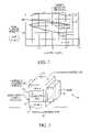
- FIG. 3illustrates an example of a vertical transistor according to a first embodiment of the present invention
- FIGS. 4A–4Cillustrate embodiments of the present invention
- FIG. 5illustrates a crystal and various planes therein
- FIG. 6Adepicts the recrystallization of thin films a prior art horizontal transistor
- FIG. 6Bdepicts vertical transistors according to the present invention.
- FIG. 7shows a schematic diagram of a processing system including a DRAM or an SRAM, or both, having CMOS transistors fabricated according to the present invention.
- FIG. 3illustrates an example of a vertical device 10 , used in logic or memory applications.
- Vertical device 10is formed on the sidewalls of intersecting trenches.
- device 10includes, from top to bottom, a drain 12 , a conduction area 14 , and a source 16 , all of which are formed on a substrate or insulator 18 .
- Gate 20is formed on the side of the device 10 .
- the upper drain surface 12 - ais formed on a (100) crystal orientation.
- conductionoccurs in the ⁇ 100> direction, from the source to the drain.
- the sidewalls 10 - a of the device 10are in this example formed on a (110) crystal orientation.
- Such devices as that pictured at 10 in FIG. 3have the features of SOI devices, and may be fabricated on conventional bulk wafers via a conventional process. Similar vertical devices have been proposed for electrically programmable devices and SRAMs.
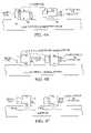
- the first maskdefines a set of parallel stripes for etching trenches to define section areas upon which the devices will be built.
- the starting waferis a (100) orientation, for example, a p-type orientation wafer 40 , and the first mask is oriented along the ⁇ 110> direction
- the trenches 46 , 48which are formed prior to the n-p-n structure is built vertically, will be the (110) planes.
- the process used, if followed to completion,will result in vertical NFET and PFET devices having channels lying in the (110) plane with a current flow in the ⁇ 100> direction.
- the vertical transistorseach include a lower doped section 42 , 44 , which is either n+ or p+, with the lower doped sections 42 , 44 being formed in trenches 46 , 48 respectively. According to the data in FIG.
- the surface hole mobility of the room temperature PFET thus formedis 70% greater than that of the conventional planar device on the (100) plane. Also, the resultant device current is correspondingly higher. Because circuit performance is limited by PFET current, a corresponding performance improvement will occur. The enhanced performance will not be as great as if the device were formed such that channel conduction is in the ⁇ 110> direction parallel to the wafer surfaces, but the vertical transistors are easier to fabricate and occupy less surface area and thus have a higher density of transistors.
- Vertical (110) surfaces 50 perpendicular to the wafer surfacecan also be formed by etching the (111) surface orientation wafers as illustrated in FIG. 5 , the (110) and (111) surfaces being at 90 degrees to one another.
- the surface mobility of holesis 80% higher on the (111) surfaces than on the (100) surfaces.
- (111) surfacescan also be used as illustrated in FIG. 4B , as can higher order surfaces such as (311), (511) and other higher order surfaces.
- (111) and higher order surfaceshave not been widely utilized in CMOS technology, since the higher surface state charge density is detrimental to micron sized dimensional technology, but is irrelevant in deep sub-micron technology.
- Higher order surfacescan be used for deep sub-micron CMOS technology by etching (110) surface oriented wafers and forming vertical sidewalls. A wide variety of orientations can be formed depending upon the orientation of the mask used for etching.
- the thus formed transistorshave substantially matching characteristics, such as the switching characteristics of the transistors and the current characteristics of the transistors.
- FIG. 5illustrates perpendicular (111) and (110) planes. However, as shown below, the dot product of two vectors (a, b, c) and (x, y, z) is ax+by+cz and if this sum is zero then the planes are perpendicular.
- the (01 ⁇ )is equivalent to the (110) plane and thus, by taking the dot product of (311) and (01 ⁇ ), (511) and (01 ⁇ ), and (111) and (01 ⁇ ), which is also known to be equivalent to the (110) plane, then the results show that the (311) and (511) planes are perpendicular to the (011) plane. The results also show that the (111) plane is perpendicular to the (110) plane in that all turn out to be have a zero sum vector dot product.
- Other higher order surfacessuch as the (311) surface and the (511) surface can be produced by rotation of the etch mask. As shown in FIG. 4B , these planes, i.e. the (311) and (511) surfaces, can be perpendicular to the (110) surface.
- the characteristics of the (311) surfacehave been previously investigated for use in MOS technology, and the (511) surfaces have some unique properties and can have a very low surface state density.
- Transistorscan be formed in bulk along these sidewalls as shown in FIGS. 4A and 4B , as well as in SOI technology as shown in FIG. 4C .
- FIG. 6Billustrates a vertical transistor formed in thin film transistor technology and the current flow therein.
- the vertical transistorhas a front gate 70 and may have a back gate 72 .
- the front gate 70 and the back gate 72allow the current to flow vertically from source to drain rather than across grain boundaries as in the horizontal transistors of FIG. 6A .
- a body contactmay be used rather than a back gate.
- FIG. 7illustrates a processor-based system including a CPU 100 , input/out devices 110 , either SRAM unit 120 or DRAM unit 130 , either of which functions as a memory device, and a storage device such as a RAM 140 .
- the DRAM 130 or the SRAM 120include peripheral circuits having NMOS and PMOS transistors fabricated in accordance with the method of the present invention.
- the NMOS DRAM or SRAM transistorsare as pictured in FIGS. 4A and 4C , as are the PMOS transistors, which differ from the NMOS transistors by switching the n type semiconductor material for p type semiconductor material.
- the transistors of the DRAM or SRAMare formed on the (111), (311), (511) or higher order crystal surfaces of the silicon substrate.
- the RAM 140is connected to the NMOS/PMOS DRAM or SRAM transistor pair.
Landscapes
- Metal-Oxide And Bipolar Metal-Oxide Semiconductor Integrated Circuits (AREA)
- Thin Film Transistor (AREA)
Abstract
Description
Claims (7)
Priority Applications (1)
| Application Number | Priority Date | Filing Date | Title |
|---|---|---|---|
| US10/222,997US7217606B2 (en) | 1999-08-13 | 2002-08-19 | Method of forming vertical sub-micron CMOS transistors on (110), (111), (311), (511), and higher order surfaces of bulk, soi and thin film structures |
Applications Claiming Priority (2)
| Application Number | Priority Date | Filing Date | Title |
|---|---|---|---|
| US09/386,313US6483171B1 (en) | 1999-08-13 | 1999-08-13 | Vertical sub-micron CMOS transistors on (110), (111), (311), (511), and higher order surfaces of bulk, SOI and thin film structures and method of forming same |
| US10/222,997US7217606B2 (en) | 1999-08-13 | 2002-08-19 | Method of forming vertical sub-micron CMOS transistors on (110), (111), (311), (511), and higher order surfaces of bulk, soi and thin film structures |
Related Parent Applications (1)
| Application Number | Title | Priority Date | Filing Date |
|---|---|---|---|
| US09/386,313DivisionUS6483171B1 (en) | 1999-08-13 | 1999-08-13 | Vertical sub-micron CMOS transistors on (110), (111), (311), (511), and higher order surfaces of bulk, SOI and thin film structures and method of forming same |
Publications (2)
| Publication Number | Publication Date |
|---|---|
| US20040161886A1 US20040161886A1 (en) | 2004-08-19 |
| US7217606B2true US7217606B2 (en) | 2007-05-15 |
Family
ID=23525078
Family Applications (2)
| Application Number | Title | Priority Date | Filing Date |
|---|---|---|---|
| US09/386,313Expired - LifetimeUS6483171B1 (en) | 1999-08-13 | 1999-08-13 | Vertical sub-micron CMOS transistors on (110), (111), (311), (511), and higher order surfaces of bulk, SOI and thin film structures and method of forming same |
| US10/222,997Expired - Fee RelatedUS7217606B2 (en) | 1999-08-13 | 2002-08-19 | Method of forming vertical sub-micron CMOS transistors on (110), (111), (311), (511), and higher order surfaces of bulk, soi and thin film structures |
Family Applications Before (1)
| Application Number | Title | Priority Date | Filing Date |
|---|---|---|---|
| US09/386,313Expired - LifetimeUS6483171B1 (en) | 1999-08-13 | 1999-08-13 | Vertical sub-micron CMOS transistors on (110), (111), (311), (511), and higher order surfaces of bulk, SOI and thin film structures and method of forming same |
Country Status (1)
| Country | Link |
|---|---|
| US (2) | US6483171B1 (en) |
Cited By (10)
| Publication number | Priority date | Publication date | Assignee | Title |
|---|---|---|---|---|
| US20070158739A1 (en)* | 2006-01-06 | 2007-07-12 | International Business Machines Corporation | Higher performance CMOS on (110) wafers |
| US20070221989A1 (en)* | 2006-03-21 | 2007-09-27 | The-Tu Chau | Ultra-low drain-source resistance power MOSFET |
| US20070262360A1 (en)* | 2005-12-22 | 2007-11-15 | Deva Pattanayak | High mobility power metal-oxide semiconductor field-effect transistors |
| US20090197379A1 (en)* | 2004-01-27 | 2009-08-06 | Leslie Terrence C | Selective epitaxy vertical integrated circuit components and methods |
| US9263586B2 (en) | 2014-06-06 | 2016-02-16 | Taiwan Semiconductor Manufacturing Company, Ltd. | Quantum well fin-like field effect transistor (QWFinFET) having a two-section combo QW structure |
| US9412833B2 (en) | 2005-03-11 | 2016-08-09 | Vishay-Siliconix | Narrow semiconductor trench structure |
| US10354920B2 (en) | 2011-11-22 | 2019-07-16 | Taiwan Semiconductor Manufacturing Company | Methods and apparatus for MOS capacitors in replacement gate process |
| US10453841B2 (en) | 2015-09-25 | 2019-10-22 | International Business Machines Corporation | Orientation engineering in complementary metal oxide semiconductor fin field effect transistor integration for increased mobility and sharper junction |
| US11469225B2 (en) | 2020-10-16 | 2022-10-11 | Globalfoundries U.S. Inc. | Device integration schemes leveraging a bulk semiconductor substrate having a <111 > crystal orientation |
| EP4010930A4 (en)* | 2019-08-09 | 2023-03-01 | Micron Technology, Inc. | TRANSISTOR AND METHOD OF MAKING TRANSISTORS |
Families Citing this family (109)
| Publication number | Priority date | Publication date | Assignee | Title |
|---|---|---|---|---|
| US6642579B2 (en)* | 2001-08-28 | 2003-11-04 | International Business Machines Corporation | Method of reducing the extrinsic body resistance in a silicon-on-insulator body contacted MOSFET |
| US6967351B2 (en)* | 2001-12-04 | 2005-11-22 | International Business Machines Corporation | Finfet SRAM cell using low mobility plane for cell stability and method for forming |
| US8080459B2 (en)* | 2002-09-24 | 2011-12-20 | Vishay-Siliconix | Self aligned contact in a semiconductor device and method of fabricating the same |
| US6611029B1 (en)* | 2002-11-08 | 2003-08-26 | Advanced Micro Devices, Inc. | Double gate semiconductor device having separate gates |
| US6853020B1 (en) | 2002-11-08 | 2005-02-08 | Advanced Micro Devices, Inc. | Double-gate semiconductor device |
| US7388259B2 (en)* | 2002-11-25 | 2008-06-17 | International Business Machines Corporation | Strained finFET CMOS device structures |
| SG124265A1 (en)* | 2002-12-02 | 2006-08-30 | Tadahiro Ohmi | Semiconductor device and method of manufacturing the same |
| US7148526B1 (en) | 2003-01-23 | 2006-12-12 | Advanced Micro Devices, Inc. | Germanium MOSFET devices and methods for making same |
| US6902962B2 (en)* | 2003-04-04 | 2005-06-07 | Taiwan Semiconductor Manufacturing Company, Ltd. | Silicon-on-insulator chip with multiple crystal orientations |
| US6974733B2 (en)* | 2003-06-16 | 2005-12-13 | Intel Corporation | Double-gate transistor with enhanced carrier mobility |
| US7148559B2 (en)* | 2003-06-20 | 2006-12-12 | International Business Machines Corporation | Substrate engineering for optimum CMOS device performance |
| US7410846B2 (en)* | 2003-09-09 | 2008-08-12 | International Business Machines Corporation | Method for reduced N+ diffusion in strained Si on SiGe substrate |
| US6887751B2 (en) | 2003-09-12 | 2005-05-03 | International Business Machines Corporation | MOSFET performance improvement using deformation in SOI structure |
| US7170126B2 (en)* | 2003-09-16 | 2007-01-30 | International Business Machines Corporation | Structure of vertical strained silicon devices |
| US6872641B1 (en)* | 2003-09-23 | 2005-03-29 | International Business Machines Corporation | Strained silicon on relaxed sige film with uniform misfit dislocation density |
| US7144767B2 (en)* | 2003-09-23 | 2006-12-05 | International Business Machines Corporation | NFETs using gate induced stress modulation |
| US7119403B2 (en) | 2003-10-16 | 2006-10-10 | International Business Machines Corporation | High performance strained CMOS devices |
| US7303949B2 (en) | 2003-10-20 | 2007-12-04 | International Business Machines Corporation | High performance stress-enhanced MOSFETs using Si:C and SiGe epitaxial source/drain and method of manufacture |
| US7037770B2 (en) | 2003-10-20 | 2006-05-02 | International Business Machines Corporation | Method of manufacturing strained dislocation-free channels for CMOS |
| US7319258B2 (en)* | 2003-10-31 | 2008-01-15 | Taiwan Semiconductor Manufacturing Company, Ltd. | Semiconductor-on-insulator chip with<100>-oriented transistors |
| US7129126B2 (en) | 2003-11-05 | 2006-10-31 | International Business Machines Corporation | Method and structure for forming strained Si for CMOS devices |
| US7015082B2 (en)* | 2003-11-06 | 2006-03-21 | International Business Machines Corporation | High mobility CMOS circuits |
| US7029964B2 (en) | 2003-11-13 | 2006-04-18 | International Business Machines Corporation | Method of manufacturing a strained silicon on a SiGe on SOI substrate |
| US7122849B2 (en)* | 2003-11-14 | 2006-10-17 | International Business Machines Corporation | Stressed semiconductor device structures having granular semiconductor material |
| US7247534B2 (en) | 2003-11-19 | 2007-07-24 | International Business Machines Corporation | Silicon device on Si:C-OI and SGOI and method of manufacture |
| US7091566B2 (en)* | 2003-11-20 | 2006-08-15 | International Business Machines Corp. | Dual gate FinFet |
| US7198995B2 (en) | 2003-12-12 | 2007-04-03 | International Business Machines Corporation | Strained finFETs and method of manufacture |
| KR100571827B1 (en)* | 2003-12-17 | 2006-04-17 | 삼성전자주식회사 | Thin Film Transistor and Manufacturing Method Thereof |
| US7247912B2 (en)* | 2004-01-05 | 2007-07-24 | International Business Machines Corporation | Structures and methods for making strained MOSFETs |
| US7118999B2 (en)* | 2004-01-16 | 2006-10-10 | International Business Machines Corporation | Method and apparatus to increase strain effect in a transistor channel |
| US7202132B2 (en) | 2004-01-16 | 2007-04-10 | International Business Machines Corporation | Protecting silicon germanium sidewall with silicon for strained silicon/silicon germanium MOSFETs |
| US7381609B2 (en)* | 2004-01-16 | 2008-06-03 | International Business Machines Corporation | Method and structure for controlling stress in a transistor channel |
| US8217450B1 (en) | 2004-02-03 | 2012-07-10 | GlobalFoundries, Inc. | Double-gate semiconductor device with gate contacts formed adjacent sidewalls of a fin |
| US7923782B2 (en)* | 2004-02-27 | 2011-04-12 | International Business Machines Corporation | Hybrid SOI/bulk semiconductor transistors |
| US7205206B2 (en) | 2004-03-03 | 2007-04-17 | International Business Machines Corporation | Method of fabricating mobility enhanced CMOS devices |
| US7223994B2 (en) | 2004-06-03 | 2007-05-29 | International Business Machines Corporation | Strained Si on multiple materials for bulk or SOI substrates |
| US7132751B2 (en)* | 2004-06-22 | 2006-11-07 | Intel Corporation | Memory cell using silicon carbide |
| TWI463526B (en)* | 2004-06-24 | 2014-12-01 | Ibm | Method for improving stress-induced CMOS components and components prepared by the method |
| US7288443B2 (en)* | 2004-06-29 | 2007-10-30 | International Business Machines Corporation | Structures and methods for manufacturing p-type MOSFET with graded embedded silicon-germanium source-drain and/or extension |
| US7384829B2 (en) | 2004-07-23 | 2008-06-10 | International Business Machines Corporation | Patterned strained semiconductor substrate and device |
| US7160769B2 (en)* | 2004-10-20 | 2007-01-09 | Freescale Semiconductor, Inc. | Channel orientation to enhance transistor performance |
| US7173312B2 (en)* | 2004-12-15 | 2007-02-06 | International Business Machines Corporation | Structure and method to generate local mechanical gate stress for MOSFET channel mobility modification |
| KR100849177B1 (en)* | 2005-01-04 | 2008-07-30 | 삼성전자주식회사 | Semiconductor integrated circuit devices employing a MOS transistor with facet channels and methods of fabricating the same |
| US7274084B2 (en)* | 2005-01-12 | 2007-09-25 | International Business Machines Corporation | Enhanced PFET using shear stress |
| US7256081B2 (en)* | 2005-02-01 | 2007-08-14 | International Business Machines Corporation | Structure and method to induce strain in a semiconductor device channel with stressed film under the gate |
| US7224033B2 (en) | 2005-02-15 | 2007-05-29 | International Business Machines Corporation | Structure and method for manufacturing strained FINFET |
| US7348610B2 (en)* | 2005-02-24 | 2008-03-25 | International Business Machines Corporation | Multiple layer and crystal plane orientation semiconductor substrate |
| US7545004B2 (en) | 2005-04-12 | 2009-06-09 | International Business Machines Corporation | Method and structure for forming strained devices |
| US7544577B2 (en)* | 2005-08-26 | 2009-06-09 | International Business Machines Corporation | Mobility enhancement in SiGe heterojunction bipolar transistors |
| US7202513B1 (en)* | 2005-09-29 | 2007-04-10 | International Business Machines Corporation | Stress engineering using dual pad nitride with selective SOI device architecture |
| US7575975B2 (en)* | 2005-10-31 | 2009-08-18 | Freescale Semiconductor, Inc. | Method for forming a planar and vertical semiconductor structure having a strained semiconductor layer |
| US7615806B2 (en) | 2005-10-31 | 2009-11-10 | Freescale Semiconductor, Inc. | Method for forming a semiconductor structure and structure thereof |
| US20070099360A1 (en)* | 2005-11-03 | 2007-05-03 | International Business Machines Corporation | Integrated circuits having strained channel field effect transistors and methods of making |
| US7655511B2 (en) | 2005-11-03 | 2010-02-02 | International Business Machines Corporation | Gate electrode stress control for finFET performance enhancement |
| US7785950B2 (en)* | 2005-11-10 | 2010-08-31 | International Business Machines Corporation | Dual stress memory technique method and related structure |
| US7348638B2 (en)* | 2005-11-14 | 2008-03-25 | International Business Machines Corporation | Rotational shear stress for charge carrier mobility modification |
| US7709317B2 (en)* | 2005-11-14 | 2010-05-04 | International Business Machines Corporation | Method to increase strain enhancement with spacerless FET and dual liner process |
| US7564081B2 (en) | 2005-11-30 | 2009-07-21 | International Business Machines Corporation | finFET structure with multiply stressed gate electrode |
| US7776695B2 (en)* | 2006-01-09 | 2010-08-17 | International Business Machines Corporation | Semiconductor device structure having low and high performance devices of same conductive type on same substrate |
| US7635620B2 (en) | 2006-01-10 | 2009-12-22 | International Business Machines Corporation | Semiconductor device structure having enhanced performance FET device |
| JP2007189008A (en)* | 2006-01-12 | 2007-07-26 | Elpida Memory Inc | Semiconductor memory device and manufacturing method thereof |
| US7691698B2 (en) | 2006-02-21 | 2010-04-06 | International Business Machines Corporation | Pseudomorphic Si/SiGe/Si body device with embedded SiGe source/drain |
| US7473946B2 (en)* | 2006-02-22 | 2009-01-06 | International Business Machines Corporation | CMOS structure and method including multiple crystallographic planes |
| US7615418B2 (en)* | 2006-04-28 | 2009-11-10 | International Business Machines Corporation | High performance stress-enhance MOSFET and method of manufacture |
| US7521307B2 (en)* | 2006-04-28 | 2009-04-21 | International Business Machines Corporation | CMOS structures and methods using self-aligned dual stressed layers |
| US7608489B2 (en)* | 2006-04-28 | 2009-10-27 | International Business Machines Corporation | High performance stress-enhance MOSFET and method of manufacture |
| US8853746B2 (en)* | 2006-06-29 | 2014-10-07 | International Business Machines Corporation | CMOS devices with stressed channel regions, and methods for fabricating the same |
| US7790540B2 (en) | 2006-08-25 | 2010-09-07 | International Business Machines Corporation | Structure and method to use low k stress liner to reduce parasitic capacitance |
| US8754446B2 (en)* | 2006-08-30 | 2014-06-17 | International Business Machines Corporation | Semiconductor structure having undercut-gate-oxide gate stack enclosed by protective barrier material |
| US7462522B2 (en) | 2006-08-30 | 2008-12-09 | International Business Machines Corporation | Method and structure for improving device performance variation in dual stress liner technology |
| US7649243B2 (en)* | 2006-11-06 | 2010-01-19 | International Business Machines Corporation | Semiconductor structures incorporating multiple crystallographic planes and methods for fabrication thereof |
| US9437729B2 (en) | 2007-01-08 | 2016-09-06 | Vishay-Siliconix | High-density power MOSFET with planarized metalization |
| US9947770B2 (en)* | 2007-04-03 | 2018-04-17 | Vishay-Siliconix | Self-aligned trench MOSFET and method of manufacture |
| US7615435B2 (en)* | 2007-07-31 | 2009-11-10 | International Business Machines Corporation | Semiconductor device and method of manufacture |
| US8115254B2 (en) | 2007-09-25 | 2012-02-14 | International Business Machines Corporation | Semiconductor-on-insulator structures including a trench containing an insulator stressor plug and method of fabricating same |
| US9484451B2 (en) | 2007-10-05 | 2016-11-01 | Vishay-Siliconix | MOSFET active area and edge termination area charge balance |
| US8183628B2 (en)* | 2007-10-29 | 2012-05-22 | Unisantis Electronics Singapore Pte Ltd. | Semiconductor structure and method of fabricating the semiconductor structure |
| US8492846B2 (en) | 2007-11-15 | 2013-07-23 | International Business Machines Corporation | Stress-generating shallow trench isolation structure having dual composition |
| US8598650B2 (en)* | 2008-01-29 | 2013-12-03 | Unisantis Electronics Singapore Pte Ltd. | Semiconductor device and production method therefor |
| JP5317343B2 (en)* | 2009-04-28 | 2013-10-16 | ユニサンティス エレクトロニクス シンガポール プライベート リミテッド | Semiconductor device and manufacturing method thereof |
| US9443974B2 (en)* | 2009-08-27 | 2016-09-13 | Vishay-Siliconix | Super junction trench power MOSFET device fabrication |
| US9425306B2 (en) | 2009-08-27 | 2016-08-23 | Vishay-Siliconix | Super junction trench power MOSFET devices |
| JP5356970B2 (en) | 2009-10-01 | 2013-12-04 | ユニサンティス エレクトロニクス シンガポール プライベート リミテッド | Semiconductor device |
| US9431530B2 (en) | 2009-10-20 | 2016-08-30 | Vishay-Siliconix | Super-high density trench MOSFET |
| JP4912513B2 (en)* | 2010-03-08 | 2012-04-11 | ユニサンティス エレクトロニクス シンガポール プライベート リミテッド | Solid-state imaging device |
| US8487357B2 (en) | 2010-03-12 | 2013-07-16 | Unisantis Electronics Singapore Pte Ltd. | Solid state imaging device having high sensitivity and high pixel density |
| US8598006B2 (en) | 2010-03-16 | 2013-12-03 | International Business Machines Corporation | Strain preserving ion implantation methods |
| JP5066590B2 (en) | 2010-06-09 | 2012-11-07 | ユニサンティス エレクトロニクス シンガポール プライベート リミテッド | Semiconductor device and manufacturing method thereof |
| JP5087655B2 (en) | 2010-06-15 | 2012-12-05 | ユニサンティス エレクトロニクス シンガポール プライベート リミテッド | Semiconductor device and manufacturing method thereof |
| US8637898B2 (en) | 2011-01-26 | 2014-01-28 | Triquint Semiconductor, Inc. | Linear voltage-controlled current source |
| US8564034B2 (en) | 2011-09-08 | 2013-10-22 | Unisantis Electronics Singapore Pte. Ltd. | Solid-state imaging device |
| US8669601B2 (en) | 2011-09-15 | 2014-03-11 | Unisantis Electronics Singapore Pte. Ltd. | Method for producing semiconductor device and semiconductor device having pillar-shaped semiconductor |
| US8772175B2 (en) | 2011-12-19 | 2014-07-08 | Unisantis Electronics Singapore Pte. Ltd. | Method for manufacturing semiconductor device and semiconductor device |
| US8916478B2 (en) | 2011-12-19 | 2014-12-23 | Unisantis Electronics Singapore Pte. Ltd. | Method for manufacturing semiconductor device and semiconductor device |
| US8748938B2 (en) | 2012-02-20 | 2014-06-10 | Unisantis Electronics Singapore Pte. Ltd. | Solid-state imaging device |
| US9842911B2 (en) | 2012-05-30 | 2017-12-12 | Vishay-Siliconix | Adaptive charge balanced edge termination |
| JP2014093319A (en)* | 2012-10-31 | 2014-05-19 | Toshiba Corp | Semiconductor device and method for manufacturing the same |
| KR102046761B1 (en) | 2013-01-14 | 2019-12-02 | 삼성전자 주식회사 | Nonvolatile memory device |
| US9006798B2 (en)* | 2013-05-03 | 2015-04-14 | Infineon Technologies Ag | Semiconductor device including trench transistor cell array and manufacturing method |
| JP5688190B1 (en)* | 2013-09-03 | 2015-03-25 | ユニサンティス エレクトロニクス シンガポール プライベート リミテッドUnisantis Electronics Singapore Pte Ltd. | Semiconductor device |
| US9887259B2 (en) | 2014-06-23 | 2018-02-06 | Vishay-Siliconix | Modulated super junction power MOSFET devices |
| US9882044B2 (en) | 2014-08-19 | 2018-01-30 | Vishay-Siliconix | Edge termination for super-junction MOSFETs |
| US10234486B2 (en) | 2014-08-19 | 2019-03-19 | Vishay/Siliconix | Vertical sense devices in vertical trench MOSFET |
| US9431536B1 (en) | 2015-03-16 | 2016-08-30 | Taiwan Semiconductor Manufacturing Co., Ltd. | Semiconductor device structure with raised source/drain having cap element |
| US9431305B1 (en)* | 2015-12-18 | 2016-08-30 | International Business Machines Corporation | Vertical transistor fabrication and devices |
| US9859421B1 (en)* | 2016-09-21 | 2018-01-02 | International Business Machines Corporation | Vertical field effect transistor with subway etch replacement metal gate |
| CN110098250B (en)* | 2018-01-31 | 2022-07-05 | 中国科学院微电子研究所 | Vertical device with body region, method for manufacturing the same, and corresponding electronic device |
| US11195764B2 (en)* | 2018-04-04 | 2021-12-07 | International Business Machines Corporation | Vertical transport field-effect transistors having germanium channel surfaces |
| US12271306B2 (en)* | 2021-03-27 | 2025-04-08 | Intel Corporation | Integrated three-dimensional (3D) DRAM cache |
Citations (21)
| Publication number | Priority date | Publication date | Assignee | Title |
|---|---|---|---|---|
| US3603848A (en) | 1969-02-27 | 1971-09-07 | Tokyo Shibaura Electric Co | Complementary field-effect-type semiconductor device |
| US4236166A (en)* | 1979-07-05 | 1980-11-25 | Bell Telephone Laboratories, Incorporated | Vertical field effect transistor |
| US4670768A (en)* | 1983-12-16 | 1987-06-02 | Hitachi, Ltd. | Complementary MOS integrated circuits having vertical channel FETs |
| US4768076A (en) | 1984-09-14 | 1988-08-30 | Hitachi, Ltd. | Recrystallized CMOS with different crystal planes |
| US4857986A (en) | 1985-10-17 | 1989-08-15 | Kabushiki Kaisha Toshiba | Short channel CMOS on 110 crystal plane |
| US5227660A (en)* | 1987-11-09 | 1993-07-13 | Hitachi, Ltd. | Semiconductor device |
| US5296403A (en)* | 1990-01-31 | 1994-03-22 | Research Development Corp. Of Japan | Method of manufacturing a static induction field-effect transistor |
| US5384473A (en)* | 1991-10-01 | 1995-01-24 | Kabushiki Kaisha Toshiba | Semiconductor body having element formation surfaces with different orientations |
| US5616935A (en) | 1994-02-08 | 1997-04-01 | Semiconductor Energy Laboratory Co., Ltd. | Semiconductor integrated circuit having N-channel and P-channel transistors |
| US5691230A (en)* | 1996-09-04 | 1997-11-25 | Micron Technology, Inc. | Technique for producing small islands of silicon on insulator |
| US5883012A (en)* | 1995-12-21 | 1999-03-16 | Motorola, Inc. | Method of etching a trench into a semiconductor substrate |
| US5895948A (en) | 1996-09-27 | 1999-04-20 | Nec Corporation | Semiconductor device and fabrication process thereof |
| US5942768A (en) | 1994-10-07 | 1999-08-24 | Semionductor Energy Laboratory Co., Ltd. | Semiconductor device having improved crystal orientation |
| US5963800A (en) | 1995-06-16 | 1999-10-05 | Interuniversitair Micro-Elektronica Centrum (Imec Vzw) | CMOS integration process having vertical channel |
| US5991225A (en) | 1998-02-27 | 1999-11-23 | Micron Technology, Inc. | Programmable memory address decode array with vertical transistors |
| US6037610A (en) | 1993-05-26 | 2000-03-14 | Semiconductor Energy Laboratory Co., Ltd. | Transistor and semiconductor device having columnar crystals |
| US6114205A (en)* | 1998-10-30 | 2000-09-05 | Sony Corporation | Epitaxial channel vertical MOS transistor |
| US6245615B1 (en)* | 1999-08-31 | 2001-06-12 | Micron Technology, Inc. | Method and apparatus on (110) surfaces of silicon structures with conduction in the <110> direction |
| US6307214B1 (en) | 1997-06-06 | 2001-10-23 | Semiconductor Energy Laboratory Co., Ltd. | Semiconductor thin film and semiconductor device |
| US6383871B1 (en)* | 1999-08-31 | 2002-05-07 | Micron Technology, Inc. | Method of forming multiple oxide thicknesses for merged memory and logic applications |
| US6436748B1 (en)* | 1999-08-31 | 2002-08-20 | Micron Technology, Inc. | Method for fabricating CMOS transistors having matching characteristics and apparatus formed thereby |
- 1999
- 1999-08-13USUS09/386,313patent/US6483171B1/ennot_activeExpired - Lifetime
- 2002
- 2002-08-19USUS10/222,997patent/US7217606B2/ennot_activeExpired - Fee Related
Patent Citations (21)
| Publication number | Priority date | Publication date | Assignee | Title |
|---|---|---|---|---|
| US3603848A (en) | 1969-02-27 | 1971-09-07 | Tokyo Shibaura Electric Co | Complementary field-effect-type semiconductor device |
| US4236166A (en)* | 1979-07-05 | 1980-11-25 | Bell Telephone Laboratories, Incorporated | Vertical field effect transistor |
| US4670768A (en)* | 1983-12-16 | 1987-06-02 | Hitachi, Ltd. | Complementary MOS integrated circuits having vertical channel FETs |
| US4768076A (en) | 1984-09-14 | 1988-08-30 | Hitachi, Ltd. | Recrystallized CMOS with different crystal planes |
| US4857986A (en) | 1985-10-17 | 1989-08-15 | Kabushiki Kaisha Toshiba | Short channel CMOS on 110 crystal plane |
| US5227660A (en)* | 1987-11-09 | 1993-07-13 | Hitachi, Ltd. | Semiconductor device |
| US5296403A (en)* | 1990-01-31 | 1994-03-22 | Research Development Corp. Of Japan | Method of manufacturing a static induction field-effect transistor |
| US5384473A (en)* | 1991-10-01 | 1995-01-24 | Kabushiki Kaisha Toshiba | Semiconductor body having element formation surfaces with different orientations |
| US6037610A (en) | 1993-05-26 | 2000-03-14 | Semiconductor Energy Laboratory Co., Ltd. | Transistor and semiconductor device having columnar crystals |
| US5616935A (en) | 1994-02-08 | 1997-04-01 | Semiconductor Energy Laboratory Co., Ltd. | Semiconductor integrated circuit having N-channel and P-channel transistors |
| US5942768A (en) | 1994-10-07 | 1999-08-24 | Semionductor Energy Laboratory Co., Ltd. | Semiconductor device having improved crystal orientation |
| US5963800A (en) | 1995-06-16 | 1999-10-05 | Interuniversitair Micro-Elektronica Centrum (Imec Vzw) | CMOS integration process having vertical channel |
| US5883012A (en)* | 1995-12-21 | 1999-03-16 | Motorola, Inc. | Method of etching a trench into a semiconductor substrate |
| US5691230A (en)* | 1996-09-04 | 1997-11-25 | Micron Technology, Inc. | Technique for producing small islands of silicon on insulator |
| US5895948A (en) | 1996-09-27 | 1999-04-20 | Nec Corporation | Semiconductor device and fabrication process thereof |
| US6307214B1 (en) | 1997-06-06 | 2001-10-23 | Semiconductor Energy Laboratory Co., Ltd. | Semiconductor thin film and semiconductor device |
| US5991225A (en) | 1998-02-27 | 1999-11-23 | Micron Technology, Inc. | Programmable memory address decode array with vertical transistors |
| US6114205A (en)* | 1998-10-30 | 2000-09-05 | Sony Corporation | Epitaxial channel vertical MOS transistor |
| US6245615B1 (en)* | 1999-08-31 | 2001-06-12 | Micron Technology, Inc. | Method and apparatus on (110) surfaces of silicon structures with conduction in the <110> direction |
| US6383871B1 (en)* | 1999-08-31 | 2002-05-07 | Micron Technology, Inc. | Method of forming multiple oxide thicknesses for merged memory and logic applications |
| US6436748B1 (en)* | 1999-08-31 | 2002-08-20 | Micron Technology, Inc. | Method for fabricating CMOS transistors having matching characteristics and apparatus formed thereby |
Non-Patent Citations (7)
Cited By (26)
| Publication number | Priority date | Publication date | Assignee | Title |
|---|---|---|---|---|
| US20090197379A1 (en)* | 2004-01-27 | 2009-08-06 | Leslie Terrence C | Selective epitaxy vertical integrated circuit components and methods |
| US7851309B2 (en)* | 2004-01-27 | 2010-12-14 | Micron Technology, Inc. | Selective epitaxy vertical integrated circuit components and methods |
| US9685524B2 (en) | 2005-03-11 | 2017-06-20 | Vishay-Siliconix | Narrow semiconductor trench structure |
| US9412833B2 (en) | 2005-03-11 | 2016-08-09 | Vishay-Siliconix | Narrow semiconductor trench structure |
| US9425043B2 (en)* | 2005-12-22 | 2016-08-23 | Vishay-Siliconix | High mobility power metal-oxide semiconductor field-effect transistors |
| US20070262360A1 (en)* | 2005-12-22 | 2007-11-15 | Deva Pattanayak | High mobility power metal-oxide semiconductor field-effect transistors |
| US20080220571A1 (en)* | 2005-12-22 | 2008-09-11 | Vishay-Siliconix | High mobility power metal-oxide semiconductor field-effect transistors |
| US9437424B2 (en) | 2005-12-22 | 2016-09-06 | Vishay-Siliconix | High mobility power metal-oxide semiconductor field-effect transistors |
| US20070158739A1 (en)* | 2006-01-06 | 2007-07-12 | International Business Machines Corporation | Higher performance CMOS on (110) wafers |
| US8409954B2 (en) | 2006-03-21 | 2013-04-02 | Vishay-Silconix | Ultra-low drain-source resistance power MOSFET |
| US20070221989A1 (en)* | 2006-03-21 | 2007-09-27 | The-Tu Chau | Ultra-low drain-source resistance power MOSFET |
| US9887266B2 (en) | 2006-03-21 | 2018-02-06 | Vishay-Siliconix | Ultra-low drain-source resistance power MOSFET |
| US10720361B2 (en) | 2011-11-22 | 2020-07-21 | Taiwan Semiconductor Manufacturing Company | Methods and apparatus for MOS capacitors in replacement gate process |
| US10354920B2 (en) | 2011-11-22 | 2019-07-16 | Taiwan Semiconductor Manufacturing Company | Methods and apparatus for MOS capacitors in replacement gate process |
| US9620633B2 (en) | 2014-06-06 | 2017-04-11 | Taiwan Semiconductor Manufacturing Company, Ltd. | Quantum well fin-like field effect transistor (QWFinFET) having a two-section combo QW structure |
| US9263586B2 (en) | 2014-06-06 | 2016-02-16 | Taiwan Semiconductor Manufacturing Company, Ltd. | Quantum well fin-like field effect transistor (QWFinFET) having a two-section combo QW structure |
| US10734385B2 (en) | 2015-09-25 | 2020-08-04 | International Business Machines Corporation | Orientation engineering in complementary metal oxide semiconductor fin field effect transistor integration for increased mobility and sharper junction |
| US10529717B2 (en) | 2015-09-25 | 2020-01-07 | International Business Machines Corporation | Orientation engineering in complementary metal oxide semiconductor fin field effect transistor integration for increased mobility and sharper junction |
| US10453841B2 (en) | 2015-09-25 | 2019-10-22 | International Business Machines Corporation | Orientation engineering in complementary metal oxide semiconductor fin field effect transistor integration for increased mobility and sharper junction |
| US10777557B2 (en) | 2015-09-25 | 2020-09-15 | International Business Machines Corporation | Orientation engineering in complementary metal oxide semiconductor fin field effect transistor integration for increased mobility and sharper junction |
| US10840247B2 (en) | 2015-09-25 | 2020-11-17 | International Business Machines Corporation | Orientation engineering in complementary metal oxide semiconductor fin field effect transistor integration for increased mobility and sharper junction |
| EP4010930A4 (en)* | 2019-08-09 | 2023-03-01 | Micron Technology, Inc. | TRANSISTOR AND METHOD OF MAKING TRANSISTORS |
| US12191354B2 (en) | 2019-08-09 | 2025-01-07 | Micron Technology, Inc. | Vertical transistors having at least 50% grain boundaries offset between top and bottom source/drain regions and the channel region that is vertically therebetween |
| US11469225B2 (en) | 2020-10-16 | 2022-10-11 | Globalfoundries U.S. Inc. | Device integration schemes leveraging a bulk semiconductor substrate having a <111 > crystal orientation |
| US12087764B2 (en) | 2020-10-16 | 2024-09-10 | Globalfoundries U.S. Inc. | Device integration schemes leveraging a bulk semiconductor substrate having a <111> crystal orientation |
| US12419098B2 (en) | 2020-10-16 | 2025-09-16 | Globalfoundries U.S. Inc. | Device integration schemes leveraging a bulk semiconductor substrate having a <111> crystal orientation |
Also Published As
| Publication number | Publication date |
|---|---|
| US6483171B1 (en) | 2002-11-19 |
| US20040161886A1 (en) | 2004-08-19 |
Similar Documents
| Publication | Publication Date | Title |
|---|---|---|
| US7217606B2 (en) | Method of forming vertical sub-micron CMOS transistors on (110), (111), (311), (511), and higher order surfaces of bulk, soi and thin film structures | |
| US6867460B1 (en) | FinFET SRAM cell with chevron FinFET logic | |
| JP4947902B2 (en) | High density dual planar device | |
| US5198379A (en) | Method of making a MOS thin film transistor with self-aligned asymmetrical structure | |
| US7075153B2 (en) | Grounded body SOI SRAM cell | |
| US7045880B2 (en) | Method and apparatus on (110) surfaces of silicon structures with conduction in the <110> direction | |
| US7087477B2 (en) | FinFET SRAM cell using low mobility plane for cell stability and method for forming | |
| US6924560B2 (en) | Compact SRAM cell with FinFET | |
| US7301206B2 (en) | Semiconductor-on-insulator SRAM configured using partially-depleted and fully-depleted transistors | |
| US7888201B2 (en) | Semiconductor-on-insulator SRAM configured using partially-depleted and fully-depleted transistors | |
| US7880231B2 (en) | Integration of a floating body memory on SOI with logic transistors on bulk substrate | |
| CN101160667B (en) | Hybrid bulk SOI 6T-SRAM cell with improved cell stability and performance | |
| US6861304B2 (en) | Semiconductor integrated circuit device and method of manufacturing thereof | |
| EP1946375B1 (en) | Highly manufacturable sram cells in substrates with hybrid crystal orientation | |
| US20090224321A1 (en) | Semiconductor device and method of manufacturing semiconductor device | |
| US20120202330A1 (en) | Semiconductor device and method of manufacturing the same | |
| JP2009520346A (en) | Substrate solution for back gate controlled SRAM with coexisting logic devices | |
| US6069390A (en) | Semiconductor integrated circuits with mesas | |
| US6300663B1 (en) | Insulated-gate field-effect transistors having different gate capacitances | |
| JP2787546B2 (en) | Method for manufacturing thin film transistor | |
| JP3082073B2 (en) | SRAM cell and method of manufacturing the same | |
| US5953606A (en) | Method for manufacturing a TFT SRAM memory device with improved performance | |
| Mukai et al. | Proposal of a logic compatible merged-type gain cell for high-density embedded DRAM's | |
| KR100654535B1 (en) | FinFET Static Memory Cell Using Reverse FIFNFC Thin Film Transistor | |
| JPH08236643A (en) | Static memory cell |
Legal Events
| Date | Code | Title | Description |
|---|---|---|---|
| STCF | Information on status: patent grant | Free format text:PATENTED CASE | |
| FEPP | Fee payment procedure | Free format text:PAYOR NUMBER ASSIGNED (ORIGINAL EVENT CODE: ASPN); ENTITY STATUS OF PATENT OWNER: LARGE ENTITY | |
| FPAY | Fee payment | Year of fee payment:4 | |
| FEPP | Fee payment procedure | Free format text:PAYER NUMBER DE-ASSIGNED (ORIGINAL EVENT CODE: RMPN); ENTITY STATUS OF PATENT OWNER: LARGE ENTITY Free format text:PAYOR NUMBER ASSIGNED (ORIGINAL EVENT CODE: ASPN); ENTITY STATUS OF PATENT OWNER: LARGE ENTITY | |
| FPAY | Fee payment | Year of fee payment:8 | |
| AS | Assignment | Owner name:U.S. BANK NATIONAL ASSOCIATION, AS COLLATERAL AGENT, CALIFORNIA Free format text:SECURITY INTEREST;ASSIGNOR:MICRON TECHNOLOGY, INC.;REEL/FRAME:038669/0001 Effective date:20160426 Owner name:U.S. BANK NATIONAL ASSOCIATION, AS COLLATERAL AGEN Free format text:SECURITY INTEREST;ASSIGNOR:MICRON TECHNOLOGY, INC.;REEL/FRAME:038669/0001 Effective date:20160426 | |
| AS | Assignment | Owner name:MORGAN STANLEY SENIOR FUNDING, INC., AS COLLATERAL AGENT, MARYLAND Free format text:PATENT SECURITY AGREEMENT;ASSIGNOR:MICRON TECHNOLOGY, INC.;REEL/FRAME:038954/0001 Effective date:20160426 Owner name:MORGAN STANLEY SENIOR FUNDING, INC., AS COLLATERAL Free format text:PATENT SECURITY AGREEMENT;ASSIGNOR:MICRON TECHNOLOGY, INC.;REEL/FRAME:038954/0001 Effective date:20160426 | |
| AS | Assignment | Owner name:U.S. BANK NATIONAL ASSOCIATION, AS COLLATERAL AGENT, CALIFORNIA Free format text:CORRECTIVE ASSIGNMENT TO CORRECT THE REPLACE ERRONEOUSLY FILED PATENT #7358718 WITH THE CORRECT PATENT #7358178 PREVIOUSLY RECORDED ON REEL 038669 FRAME 0001. ASSIGNOR(S) HEREBY CONFIRMS THE SECURITY INTEREST;ASSIGNOR:MICRON TECHNOLOGY, INC.;REEL/FRAME:043079/0001 Effective date:20160426 Owner name:U.S. BANK NATIONAL ASSOCIATION, AS COLLATERAL AGEN Free format text:CORRECTIVE ASSIGNMENT TO CORRECT THE REPLACE ERRONEOUSLY FILED PATENT #7358718 WITH THE CORRECT PATENT #7358178 PREVIOUSLY RECORDED ON REEL 038669 FRAME 0001. ASSIGNOR(S) HEREBY CONFIRMS THE SECURITY INTEREST;ASSIGNOR:MICRON TECHNOLOGY, INC.;REEL/FRAME:043079/0001 Effective date:20160426 | |
| AS | Assignment | Owner name:JPMORGAN CHASE BANK, N.A., AS COLLATERAL AGENT, ILLINOIS Free format text:SECURITY INTEREST;ASSIGNORS:MICRON TECHNOLOGY, INC.;MICRON SEMICONDUCTOR PRODUCTS, INC.;REEL/FRAME:047540/0001 Effective date:20180703 Owner name:JPMORGAN CHASE BANK, N.A., AS COLLATERAL AGENT, IL Free format text:SECURITY INTEREST;ASSIGNORS:MICRON TECHNOLOGY, INC.;MICRON SEMICONDUCTOR PRODUCTS, INC.;REEL/FRAME:047540/0001 Effective date:20180703 | |
| AS | Assignment | Owner name:MICRON TECHNOLOGY, INC., IDAHO Free format text:RELEASE BY SECURED PARTY;ASSIGNOR:U.S. BANK NATIONAL ASSOCIATION, AS COLLATERAL AGENT;REEL/FRAME:047243/0001 Effective date:20180629 | |
| FEPP | Fee payment procedure | Free format text:MAINTENANCE FEE REMINDER MAILED (ORIGINAL EVENT CODE: REM.); ENTITY STATUS OF PATENT OWNER: LARGE ENTITY | |
| LAPS | Lapse for failure to pay maintenance fees | Free format text:PATENT EXPIRED FOR FAILURE TO PAY MAINTENANCE FEES (ORIGINAL EVENT CODE: EXP.); ENTITY STATUS OF PATENT OWNER: LARGE ENTITY | |
| STCH | Information on status: patent discontinuation | Free format text:PATENT EXPIRED DUE TO NONPAYMENT OF MAINTENANCE FEES UNDER 37 CFR 1.362 | |
| FP | Lapsed due to failure to pay maintenance fee | Effective date:20190515 | |
| AS | Assignment | Owner name:MICRON TECHNOLOGY, INC., IDAHO Free format text:RELEASE BY SECURED PARTY;ASSIGNOR:MORGAN STANLEY SENIOR FUNDING, INC., AS COLLATERAL AGENT;REEL/FRAME:050937/0001 Effective date:20190731 | |
| AS | Assignment | Owner name:MICRON TECHNOLOGY, INC., IDAHO Free format text:RELEASE BY SECURED PARTY;ASSIGNOR:JPMORGAN CHASE BANK, N.A., AS COLLATERAL AGENT;REEL/FRAME:051028/0001 Effective date:20190731 Owner name:MICRON SEMICONDUCTOR PRODUCTS, INC., IDAHO Free format text:RELEASE BY SECURED PARTY;ASSIGNOR:JPMORGAN CHASE BANK, N.A., AS COLLATERAL AGENT;REEL/FRAME:051028/0001 Effective date:20190731 |