US7217603B2 - Methods of forming reacted conductive gate electrodes - Google Patents
Methods of forming reacted conductive gate electrodesDownload PDFInfo
- Publication number
- US7217603B2 US7217603B2US11/073,976US7397605AUS7217603B2US 7217603 B2US7217603 B2US 7217603B2US 7397605 AUS7397605 AUS 7397605AUS 7217603 B2US7217603 B2US 7217603B2
- Authority
- US
- United States
- Prior art keywords
- strain
- layer
- strained
- silicon
- sige
- Prior art date
- Legal status (The legal status is an assumption and is not a legal conclusion. Google has not performed a legal analysis and makes no representation as to the accuracy of the status listed.)
- Expired - Lifetime
Links
- 238000000034methodMethods0.000titleclaimsabstractdescription72
- 239000004065semiconductorSubstances0.000claimsabstractdescription74
- 229910052710siliconInorganic materials0.000claimsabstractdescription64
- 239000010703siliconSubstances0.000claimsabstractdescription64
- 239000000463materialSubstances0.000claimsabstractdescription57
- 229910052732germaniumInorganic materials0.000claimsabstractdescription27
- GNPVGFCGXDBREM-UHFFFAOYSA-Ngermanium atomChemical compound[Ge]GNPVGFCGXDBREM-UHFFFAOYSA-N0.000claimsabstractdescription25
- 229910000577Silicon-germaniumInorganic materials0.000claimsdescription93
- 239000000758substrateSubstances0.000claimsdescription85
- XUIMIQQOPSSXEZ-UHFFFAOYSA-NSiliconChemical compound[Si]XUIMIQQOPSSXEZ-UHFFFAOYSA-N0.000claimsdescription57
- FVBUAEGBCNSCDD-UHFFFAOYSA-Nsilicide(4-)Chemical compound[Si-4]FVBUAEGBCNSCDD-UHFFFAOYSA-N0.000claimsdescription36
- 229910021332silicideInorganic materials0.000claimsdescription34
- 238000002955isolationMethods0.000claimsdescription18
- 239000007769metal materialSubstances0.000claimsdescription13
- 229910021420polycrystalline siliconInorganic materials0.000claimsdescription13
- PXHVJJICTQNCMI-UHFFFAOYSA-NNickelChemical compound[Ni]PXHVJJICTQNCMI-UHFFFAOYSA-N0.000claimsdescription11
- 238000000137annealingMethods0.000claimsdescription10
- 238000000151depositionMethods0.000claimsdescription9
- 230000008021depositionEffects0.000claimsdescription5
- 229910052759nickelInorganic materials0.000claimsdescription5
- BASFCYQUMIYNBI-UHFFFAOYSA-NplatinumChemical compound[Pt]BASFCYQUMIYNBI-UHFFFAOYSA-N0.000claimsdescription5
- 239000012212insulatorSubstances0.000claimsdescription3
- 230000003647oxidationEffects0.000claimsdescription3
- 238000007254oxidation reactionMethods0.000claimsdescription3
- QCWXUUIWCKQGHC-UHFFFAOYSA-NZirconiumChemical compound[Zr]QCWXUUIWCKQGHC-UHFFFAOYSA-N0.000claimsdescription2
- 229910052697platinumInorganic materials0.000claimsdescription2
- 229910052726zirconiumInorganic materials0.000claimsdescription2
- 230000001939inductive effectEffects0.000claims18
- 229910052751metalInorganic materials0.000abstractdescription37
- 239000002184metalSubstances0.000abstractdescription37
- 239000010410layerSubstances0.000description178
- 239000000203mixtureSubstances0.000description29
- 230000015572biosynthetic processEffects0.000description24
- 238000004519manufacturing processMethods0.000description19
- 238000006243chemical reactionMethods0.000description14
- 235000012431wafersNutrition0.000description14
- 238000012545processingMethods0.000description11
- VYPSYNLAJGMNEJ-UHFFFAOYSA-NSilicium dioxideChemical compoundO=[Si]=OVYPSYNLAJGMNEJ-UHFFFAOYSA-N0.000description9
- 230000008569processEffects0.000description9
- 125000006850spacer groupChemical group0.000description8
- 229920005591polysiliconPolymers0.000description7
- 229910045601alloyInorganic materials0.000description6
- 239000000956alloySubstances0.000description6
- 239000010936titaniumSubstances0.000description6
- 239000002019doping agentSubstances0.000description5
- RTAQQCXQSZGOHL-UHFFFAOYSA-NTitaniumChemical compound[Ti]RTAQQCXQSZGOHL-UHFFFAOYSA-N0.000description4
- 230000008901benefitEffects0.000description4
- 239000010941cobaltSubstances0.000description4
- 229910017052cobaltInorganic materials0.000description4
- GUTLYIVDDKVIGB-UHFFFAOYSA-Ncobalt atomChemical compound[Co]GUTLYIVDDKVIGB-UHFFFAOYSA-N0.000description4
- 239000000377silicon dioxideSubstances0.000description4
- 229910052719titaniumInorganic materials0.000description4
- 229910006990Si1-xGexInorganic materials0.000description3
- 229910007020Si1−xGexInorganic materials0.000description3
- 239000003989dielectric materialSubstances0.000description3
- 238000002513implantationMethods0.000description3
- 235000012239silicon dioxideNutrition0.000description3
- 239000002344surface layerSubstances0.000description3
- 229910052581Si3N4Inorganic materials0.000description2
- LEVVHYCKPQWKOP-UHFFFAOYSA-N[Si].[Ge]Chemical compound[Si].[Ge]LEVVHYCKPQWKOP-UHFFFAOYSA-N0.000description2
- 238000005054agglomerationMethods0.000description2
- 230000002776aggregationEffects0.000description2
- 239000007795chemical reaction productSubstances0.000description2
- 150000001875compoundsChemical class0.000description2
- 238000013461designMethods0.000description2
- 238000011161developmentMethods0.000description2
- 238000009792diffusion processMethods0.000description2
- -1for exampleSubstances0.000description2
- 230000006872improvementEffects0.000description2
- 150000002739metalsChemical class0.000description2
- 229920000642polymerPolymers0.000description2
- 238000000926separation methodMethods0.000description2
- HQVNEWCFYHHQES-UHFFFAOYSA-Nsilicon nitrideChemical compoundN12[Si]34N5[Si]62N3[Si]51N64HQVNEWCFYHHQES-UHFFFAOYSA-N0.000description2
- 229910021341titanium silicideInorganic materials0.000description2
- RYGMFSIKBFXOCR-UHFFFAOYSA-NCopperChemical compound[Cu]RYGMFSIKBFXOCR-UHFFFAOYSA-N0.000description1
- ZOKXTWBITQBERF-UHFFFAOYSA-NMolybdenumChemical compound[Mo]ZOKXTWBITQBERF-UHFFFAOYSA-N0.000description1
- 229910052782aluminiumInorganic materials0.000description1
- XAGFODPZIPBFFR-UHFFFAOYSA-NaluminiumChemical compound[Al]XAGFODPZIPBFFR-UHFFFAOYSA-N0.000description1
- 238000005229chemical vapour depositionMethods0.000description1
- 229910052681coesiteInorganic materials0.000description1
- 229910052802copperInorganic materials0.000description1
- 239000010949copperSubstances0.000description1
- 229910052906cristobaliteInorganic materials0.000description1
- 230000007547defectEffects0.000description1
- 238000010586diagramMethods0.000description1
- 238000009826distributionMethods0.000description1
- 230000005669field effectEffects0.000description1
- 239000011521glassSubstances0.000description1
- 230000010354integrationEffects0.000description1
- 238000005468ion implantationMethods0.000description1
- 150000002500ionsChemical class0.000description1
- 238000001459lithographyMethods0.000description1
- 238000004377microelectronicMethods0.000description1
- 238000012986modificationMethods0.000description1
- 230000004048modificationEffects0.000description1
- 239000011733molybdenumSubstances0.000description1
- 229910052750molybdenumInorganic materials0.000description1
- 150000004767nitridesChemical class0.000description1
- 229920003986novolacPolymers0.000description1
- 238000000059patterningMethods0.000description1
- 238000000206photolithographyMethods0.000description1
- 229920002120photoresistant polymerPolymers0.000description1
- 238000005498polishingMethods0.000description1
- 238000003672processing methodMethods0.000description1
- 230000035484reaction timeEffects0.000description1
- 229910052814silicon oxideInorganic materials0.000description1
- 238000000992sputter etchingMethods0.000description1
- 229910052682stishoviteInorganic materials0.000description1
- 229910052905tridymiteInorganic materials0.000description1
- WFKWXMTUELFFGS-UHFFFAOYSA-NtungstenChemical compound[W]WFKWXMTUELFFGS-UHFFFAOYSA-N0.000description1
- 229910052721tungstenInorganic materials0.000description1
- 239000010937tungstenSubstances0.000description1
Images


Classifications
- H—ELECTRICITY
- H10—SEMICONDUCTOR DEVICES; ELECTRIC SOLID-STATE DEVICES NOT OTHERWISE PROVIDED FOR
- H10D—INORGANIC ELECTRIC SEMICONDUCTOR DEVICES
- H10D30/00—Field-effect transistors [FET]
- H10D30/60—Insulated-gate field-effect transistors [IGFET]
- H10D30/791—Arrangements for exerting mechanical stress on the crystal lattice of the channel regions
- H10D30/797—Arrangements for exerting mechanical stress on the crystal lattice of the channel regions being in source or drain regions, e.g. SiGe source or drain
- H—ELECTRICITY
- H01—ELECTRIC ELEMENTS
- H01L—SEMICONDUCTOR DEVICES NOT COVERED BY CLASS H10
- H01L21/00—Processes or apparatus adapted for the manufacture or treatment of semiconductor or solid state devices or of parts thereof
- H01L21/02—Manufacture or treatment of semiconductor devices or of parts thereof
- H01L21/04—Manufacture or treatment of semiconductor devices or of parts thereof the devices having potential barriers, e.g. a PN junction, depletion layer or carrier concentration layer
- H01L21/18—Manufacture or treatment of semiconductor devices or of parts thereof the devices having potential barriers, e.g. a PN junction, depletion layer or carrier concentration layer the devices having semiconductor bodies comprising elements of Group IV of the Periodic Table or AIIIBV compounds with or without impurities, e.g. doping materials
- H01L21/28—Manufacture of electrodes on semiconductor bodies using processes or apparatus not provided for in groups H01L21/20 - H01L21/268
- H01L21/28008—Making conductor-insulator-semiconductor electrodes
- H01L21/28017—Making conductor-insulator-semiconductor electrodes the insulator being formed after the semiconductor body, the semiconductor being silicon
- H01L21/28026—Making conductor-insulator-semiconductor electrodes the insulator being formed after the semiconductor body, the semiconductor being silicon characterised by the conductor
- H01L21/28035—Making conductor-insulator-semiconductor electrodes the insulator being formed after the semiconductor body, the semiconductor being silicon characterised by the conductor the final conductor layer next to the insulator being silicon, e.g. polysilicon, with or without impurities
- H01L21/28044—Making conductor-insulator-semiconductor electrodes the insulator being formed after the semiconductor body, the semiconductor being silicon characterised by the conductor the final conductor layer next to the insulator being silicon, e.g. polysilicon, with or without impurities the conductor comprising at least another non-silicon conductive layer
- H01L21/28052—Making conductor-insulator-semiconductor electrodes the insulator being formed after the semiconductor body, the semiconductor being silicon characterised by the conductor the final conductor layer next to the insulator being silicon, e.g. polysilicon, with or without impurities the conductor comprising at least another non-silicon conductive layer the conductor comprising a silicide layer formed by the silicidation reaction of silicon with a metal layer
- H—ELECTRICITY
- H01—ELECTRIC ELEMENTS
- H01L—SEMICONDUCTOR DEVICES NOT COVERED BY CLASS H10
- H01L21/00—Processes or apparatus adapted for the manufacture or treatment of semiconductor or solid state devices or of parts thereof
- H01L21/02—Manufacture or treatment of semiconductor devices or of parts thereof
- H01L21/04—Manufacture or treatment of semiconductor devices or of parts thereof the devices having potential barriers, e.g. a PN junction, depletion layer or carrier concentration layer
- H01L21/18—Manufacture or treatment of semiconductor devices or of parts thereof the devices having potential barriers, e.g. a PN junction, depletion layer or carrier concentration layer the devices having semiconductor bodies comprising elements of Group IV of the Periodic Table or AIIIBV compounds with or without impurities, e.g. doping materials
- H01L21/28—Manufacture of electrodes on semiconductor bodies using processes or apparatus not provided for in groups H01L21/20 - H01L21/268
- H01L21/28008—Making conductor-insulator-semiconductor electrodes
- H01L21/28017—Making conductor-insulator-semiconductor electrodes the insulator being formed after the semiconductor body, the semiconductor being silicon
- H01L21/28026—Making conductor-insulator-semiconductor electrodes the insulator being formed after the semiconductor body, the semiconductor being silicon characterised by the conductor
- H01L21/2807—Making conductor-insulator-semiconductor electrodes the insulator being formed after the semiconductor body, the semiconductor being silicon characterised by the conductor the final conductor layer next to the insulator being Si or Ge or C and their alloys except Si
- H—ELECTRICITY
- H01—ELECTRIC ELEMENTS
- H01L—SEMICONDUCTOR DEVICES NOT COVERED BY CLASS H10
- H01L21/00—Processes or apparatus adapted for the manufacture or treatment of semiconductor or solid state devices or of parts thereof
- H01L21/02—Manufacture or treatment of semiconductor devices or of parts thereof
- H01L21/04—Manufacture or treatment of semiconductor devices or of parts thereof the devices having potential barriers, e.g. a PN junction, depletion layer or carrier concentration layer
- H01L21/18—Manufacture or treatment of semiconductor devices or of parts thereof the devices having potential barriers, e.g. a PN junction, depletion layer or carrier concentration layer the devices having semiconductor bodies comprising elements of Group IV of the Periodic Table or AIIIBV compounds with or without impurities, e.g. doping materials
- H01L21/28—Manufacture of electrodes on semiconductor bodies using processes or apparatus not provided for in groups H01L21/20 - H01L21/268
- H01L21/28008—Making conductor-insulator-semiconductor electrodes
- H01L21/28255—Making conductor-insulator-semiconductor electrodes the insulator being formed after the semiconductor body, the semiconductor belonging to Group IV and not being elemental silicon, e.g. Ge, SiGe, SiGeC
- H—ELECTRICITY
- H01—ELECTRIC ELEMENTS
- H01L—SEMICONDUCTOR DEVICES NOT COVERED BY CLASS H10
- H01L21/00—Processes or apparatus adapted for the manufacture or treatment of semiconductor or solid state devices or of parts thereof
- H01L21/02—Manufacture or treatment of semiconductor devices or of parts thereof
- H01L21/04—Manufacture or treatment of semiconductor devices or of parts thereof the devices having potential barriers, e.g. a PN junction, depletion layer or carrier concentration layer
- H01L21/18—Manufacture or treatment of semiconductor devices or of parts thereof the devices having potential barriers, e.g. a PN junction, depletion layer or carrier concentration layer the devices having semiconductor bodies comprising elements of Group IV of the Periodic Table or AIIIBV compounds with or without impurities, e.g. doping materials
- H01L21/28—Manufacture of electrodes on semiconductor bodies using processes or apparatus not provided for in groups H01L21/20 - H01L21/268
- H01L21/283—Deposition of conductive or insulating materials for electrodes conducting electric current
- H01L21/285—Deposition of conductive or insulating materials for electrodes conducting electric current from a gas or vapour, e.g. condensation
- H01L21/28506—Deposition of conductive or insulating materials for electrodes conducting electric current from a gas or vapour, e.g. condensation of conductive layers
- H01L21/28512—Deposition of conductive or insulating materials for electrodes conducting electric current from a gas or vapour, e.g. condensation of conductive layers on semiconductor bodies comprising elements of Group IV of the Periodic Table
- H01L21/28518—Deposition of conductive or insulating materials for electrodes conducting electric current from a gas or vapour, e.g. condensation of conductive layers on semiconductor bodies comprising elements of Group IV of the Periodic Table the conductive layers comprising silicides
- H—ELECTRICITY
- H01—ELECTRIC ELEMENTS
- H01L—SEMICONDUCTOR DEVICES NOT COVERED BY CLASS H10
- H01L21/00—Processes or apparatus adapted for the manufacture or treatment of semiconductor or solid state devices or of parts thereof
- H01L21/02—Manufacture or treatment of semiconductor devices or of parts thereof
- H01L21/04—Manufacture or treatment of semiconductor devices or of parts thereof the devices having potential barriers, e.g. a PN junction, depletion layer or carrier concentration layer
- H01L21/18—Manufacture or treatment of semiconductor devices or of parts thereof the devices having potential barriers, e.g. a PN junction, depletion layer or carrier concentration layer the devices having semiconductor bodies comprising elements of Group IV of the Periodic Table or AIIIBV compounds with or without impurities, e.g. doping materials
- H01L21/30—Treatment of semiconductor bodies using processes or apparatus not provided for in groups H01L21/20 - H01L21/26
- H01L21/324—Thermal treatment for modifying the properties of semiconductor bodies, e.g. annealing, sintering
- H—ELECTRICITY
- H10—SEMICONDUCTOR DEVICES; ELECTRIC SOLID-STATE DEVICES NOT OTHERWISE PROVIDED FOR
- H10D—INORGANIC ELECTRIC SEMICONDUCTOR DEVICES
- H10D30/00—Field-effect transistors [FET]
- H10D30/01—Manufacture or treatment
- H10D30/021—Manufacture or treatment of FETs having insulated gates [IGFET]
- H10D30/0212—Manufacture or treatment of FETs having insulated gates [IGFET] using self-aligned silicidation
- H—ELECTRICITY
- H10—SEMICONDUCTOR DEVICES; ELECTRIC SOLID-STATE DEVICES NOT OTHERWISE PROVIDED FOR
- H10D—INORGANIC ELECTRIC SEMICONDUCTOR DEVICES
- H10D30/00—Field-effect transistors [FET]
- H10D30/60—Insulated-gate field-effect transistors [IGFET]
- H10D30/751—Insulated-gate field-effect transistors [IGFET] having composition variations in the channel regions
- H—ELECTRICITY
- H10—SEMICONDUCTOR DEVICES; ELECTRIC SOLID-STATE DEVICES NOT OTHERWISE PROVIDED FOR
- H10D—INORGANIC ELECTRIC SEMICONDUCTOR DEVICES
- H10D30/00—Field-effect transistors [FET]
- H10D30/60—Insulated-gate field-effect transistors [IGFET]
- H10D30/791—Arrangements for exerting mechanical stress on the crystal lattice of the channel regions
- H—ELECTRICITY
- H10—SEMICONDUCTOR DEVICES; ELECTRIC SOLID-STATE DEVICES NOT OTHERWISE PROVIDED FOR
- H10D—INORGANIC ELECTRIC SEMICONDUCTOR DEVICES
- H10D62/00—Semiconductor bodies, or regions thereof, of devices having potential barriers
- H10D62/10—Shapes, relative sizes or dispositions of the regions of the semiconductor bodies; Shapes of the semiconductor bodies
- H10D62/13—Semiconductor regions connected to electrodes carrying current to be rectified, amplified or switched, e.g. source or drain regions
- H10D62/149—Source or drain regions of field-effect devices
- H10D62/151—Source or drain regions of field-effect devices of IGFETs
- H—ELECTRICITY
- H10—SEMICONDUCTOR DEVICES; ELECTRIC SOLID-STATE DEVICES NOT OTHERWISE PROVIDED FOR
- H10D—INORGANIC ELECTRIC SEMICONDUCTOR DEVICES
- H10D62/00—Semiconductor bodies, or regions thereof, of devices having potential barriers
- H10D62/80—Semiconductor bodies, or regions thereof, of devices having potential barriers characterised by the materials
- H10D62/82—Heterojunctions
- H10D62/822—Heterojunctions comprising only Group IV materials heterojunctions, e.g. Si/Ge heterojunctions
- H—ELECTRICITY
- H10—SEMICONDUCTOR DEVICES; ELECTRIC SOLID-STATE DEVICES NOT OTHERWISE PROVIDED FOR
- H10D—INORGANIC ELECTRIC SEMICONDUCTOR DEVICES
- H10D62/00—Semiconductor bodies, or regions thereof, of devices having potential barriers
- H10D62/80—Semiconductor bodies, or regions thereof, of devices having potential barriers characterised by the materials
- H10D62/83—Semiconductor bodies, or regions thereof, of devices having potential barriers characterised by the materials being Group IV materials, e.g. B-doped Si or undoped Ge
- H10D62/832—Semiconductor bodies, or regions thereof, of devices having potential barriers characterised by the materials being Group IV materials, e.g. B-doped Si or undoped Ge being Group IV materials comprising two or more elements, e.g. SiGe
- H—ELECTRICITY
- H10—SEMICONDUCTOR DEVICES; ELECTRIC SOLID-STATE DEVICES NOT OTHERWISE PROVIDED FOR
- H10D—INORGANIC ELECTRIC SEMICONDUCTOR DEVICES
- H10D64/00—Electrodes of devices having potential barriers
- H10D64/60—Electrodes characterised by their materials
- H10D64/62—Electrodes ohmically coupled to a semiconductor
- H—ELECTRICITY
- H10—SEMICONDUCTOR DEVICES; ELECTRIC SOLID-STATE DEVICES NOT OTHERWISE PROVIDED FOR
- H10D—INORGANIC ELECTRIC SEMICONDUCTOR DEVICES
- H10D64/00—Electrodes of devices having potential barriers
- H10D64/60—Electrodes characterised by their materials
- H10D64/66—Electrodes having a conductor capacitively coupled to a semiconductor by an insulator, e.g. MIS electrodes
- H—ELECTRICITY
- H10—SEMICONDUCTOR DEVICES; ELECTRIC SOLID-STATE DEVICES NOT OTHERWISE PROVIDED FOR
- H10D—INORGANIC ELECTRIC SEMICONDUCTOR DEVICES
- H10D30/00—Field-effect transistors [FET]
- H10D30/01—Manufacture or treatment
- H10D30/021—Manufacture or treatment of FETs having insulated gates [IGFET]
- H10D30/0223—Manufacture or treatment of FETs having insulated gates [IGFET] having source and drain regions or source and drain extensions self-aligned to sides of the gate
- H10D30/0227—Manufacture or treatment of FETs having insulated gates [IGFET] having source and drain regions or source and drain extensions self-aligned to sides of the gate having both lightly-doped source and drain extensions and source and drain regions self-aligned to the sides of the gate, e.g. lightly-doped drain [LDD] MOSFET or double-diffused drain [DDD] MOSFET
Definitions
- the inventiongenerally relates to semiconductor devices, and, more particularly, to the fabrication and structure of contacts in transistors.
- conductive contacts and interconnectsMaterials and processes for forming conductive contacts and interconnects must accommodate, for example, dimensional requirements, processing temperatures, reliability needs and materials compatibility.
- Traditional aluminum-based interconnectshave gradually given way to copper interconnects for fine dimensions; cobalt silicide and other metallic materials are gradually supplanting titanium silicide source and drain contacts and titanium silicide caps on doped polycrystalline silicon gate contacts.
- SiGesilicon-germanium
- Mobility enhancements obtained from strained silicon, in combination with source-drain and gate silicidation techniques,provide the opportunity to increase speed, reduce power consumption, and provide the basis of other advances in microelectronics, such as analog and digital device integration.
- substrates that include a SiGe layercan increase fabrication complexity relative to that for conventional silicon wafer-based devices.
- formation of source and drain contacts through reaction of a metal layer, such as titanium or cobalt, with SiGe in the substratehas preferred process conditions that are different from silicide formation with relatively pure silicon.
- the inventioninvolves structures and fabrication methods for semiconductor devices that preferably have semiconductor layers including two materials in both a substrate and in a gate contact.
- the inventionprovides simplified processing for semiconductor devices, as well as improved semiconductor device structures that include compound and/or alloyed semiconductors in both contacts and substrates.
- the inventionprovides for simultaneous reaction of a metal layer to form reacted material contacts in the substrate and a reacted material upper portion of a gate contact.
- the metal layerexhibits a similar reaction behavior with the semiconductor layers in both the substrate and in the upper portion of the gate contact due to a similar composition ratio of the two materials in both semiconductor layers.
- Preferred embodiments of the inventionfeature substrates and contacts that include one or more semiconductor alloy layers of silicon and germanium.
- Preferred embodimentsinclude SiGe layers of similar composition in both a substrate and a contact; conductive portions are formed by simultaneously reacting the SiGe layers in the substrate and the contact with a metal layer.
- source and drain contacts in a substratecan be formed simultaneously with formation of a conductive upper (distal) portion of a gate contact having a portion that includes the semiconductor alloy. In this way, some processing steps are rendered unnecessary during basic device fabrication.
- Simplified processingcan be achieved in part because reaction of a metal layer with the substrate and with a semiconductor layer in a gate contact need not be decoupled to accommodate, for example, SiGe in the substrate and polycrystalline silicon in the gate.
- Proper material selectionprovides substrates and gate contacts that have similar or identical silicide formation steps. Other benefits can arise, such as lower temperature processing for silicide formation.
- the inventionfeatures transistors that include a gate electrode including SiGe in at least an upper portion of a gate contact (i.e., electrode) and a strained-silicon channel layer on a relaxed SiGe layer in a substrate.
- a gate electrode including SiGein at least an upper portion of a gate contact (i.e., electrode) and a strained-silicon channel layer on a relaxed SiGe layer in a substrate.
- the inventionfeatures a method for fabricating a semiconductor device.
- the methodincludes provision of a semiconductor layer that includes a first material and a second material.
- the semiconductor layercan be an alloy of two or more materials.
- the first and second materialscan be silicon and germanium.
- the semiconductor layercan be or include a relaxed layer.
- the relaxed layercan be part of a substrate having a portion, adjacent to the relaxed layer, with a lattice spacing mismatched to that of the relaxed layer.
- the relaxed layercan be grown on intermediate layers that accommodate mismatch to a silicon wafer.
- the relaxed layercan reside on an oxide layer.
- the methodalso includes the formation of a contact that has a portion proximal to the relaxed semiconductor layer and a portion distal to the relaxed semiconductor layer.
- the distal portionincludes the first material and the second material.
- a metal layeris formed adjacent to the relaxed semiconductor layer and adjacent to the distal portion of the contact. The metal layer is simultaneously reacted with the relaxed semiconductor layer and with the distal portion of the contact.
- the silicon and germanium of the distal portion of the contactcan have an atomic density ratio that is substantially the same as an atomic density ratio of the silicon and germanium of the relaxed semiconductor layer.
- the proximal portion of the contactcan consist essentially of silicon or essentially of germanium.
- the proximal portioncan include silicon and germanium, the atomic density ratio of the silicon and germanium of the proximal portion can differ from the atomic density ratio of the silicon and germanium of the distal portion.
- the inventionfeatures a semiconductor device.
- the deviceincludes a substrate that has a reacted conductive layer that comprises silicon, germanium and a metallic material.
- the metallic materialcan be, e.g., titanium, nickel or cobalt.
- the devicealso includes a contact that has a portion proximal to the substrate and a reacted conductive portion distal to the substrate.
- the reacted conductive distal portion of the contactincludes silicon, germanium and the same metallic material as in the substrate reacted conductive layer.
- the substratecan further include a strained semiconductor layer, for example, of silicon, adjacent to the contact.
- the inventionfeatures a semiconductor device that includes a substrate that has a reacted conductive layer comprising a first material, a second material and a metallic material.
- the deviceincludes a contact having a portion proximal to the substrate and a reacted conductive portion distal to the substrate, the distal portion comprising the first material, the second material and the metallic material.
- FIG. 1is a cross-sectional view of a conventional silicon-based MOSFET.
- FIG. 2is a cross-sectional view of an embodiment of a MOSFET that includes a strained-silicon channel layer on a SiGe layer.
- FIG. 3is a graph of sheet resistance versus anneal time.
- FIG. 4is a graph of sheet resistance versus anneal temperature.
- FIG. 5is a flowchart of an embodiment of a method of fabricating a semiconductor device.
- FIG. 6is a cross-sectional view of an embodiment of a substrate used for fabrication of an embodiment of a MOSFET.
- FIGS. 7A and 7Bare cross-sectional views of structures at intermediate steps during fabrication of an embodiment of a MOSFET, utilizing the substrate of FIG. 6 .
- FIGS. 8A and 8Bare cross-sectional views of structures at fabrication steps that follow the steps illustrated in FIGS. 7A and 7B .
- MOSmetal-oxide-semiconductor
- the inventionprovides means to avoid separation of metal layer reaction with the substrate and metal layer reaction with a polycrystalline silicon portion of a gate contact.
- the inventionfurther provides improved gate design in conjunction with the advantages of a substrate that includes a SiGe layer, among other advantages.
- MOSis here used to refer generally to semiconductor devices that include a conductive gate spaced at least by an insulting layer from a semiconducting channel layer.
- SiGeand Si 1 ⁇ x Ge x ” are here used interchangeably to refer to silicon-germanium alloys.
- siicideis here used to refer to a reaction product of a metal, silicon, and optionally other components, such as germanium.
- siicideis also used, less formally, to refer to the reaction product of a metal with an elemental semiconductor, a compound semiconductor or an alloy semiconductor.
- FIG. 1is cross-sectional view of a conventional silicon-based MOS field-effect transistor (MOSFET) 100 .
- the transistor 100includes a gate contact 120 , a pair of spacers 150 , a source 135 , a source silicide contact 130 , a gate oxide 126 , a drain 145 , a drain silicide contact 140 and a silicon substrate 110 .
- the transistor 100is electrically isolated from neighboring transistors by a shallow trench isolation (STI) portion 170 .
- STIshallow trench isolation
- the gate contact 120includes a doped, conductive polycrystalline silicon (“polysilicon”) portion 124 proximal to the gate oxide 126 and a distal gate silicide portion 122 .
- the source 135 and drain 145include doped regions formed by implantation of dopant species into the substrate 110 and annealing, with the spacers 150 controlling the distribution of dopant beneath the gate oxide 126 .
- the silicide contacts 130 , 140 and gate silicide portion 122provide good ohmic interfaces respectively to the source 135 and drain 145 and to the gate polysilicon portion 124 .
- the MOSFET 100has a surface channel, which may be defined in physical or electrical terms. Physically, the surface channel is the p-type or n-type silicon that is adjacent to (i.e., below) the gate oxide 126 and which joins the source 135 and drain 145 . Electrically, the channel is an inversion layer, which provides current flow between the source 135 and drain 145 . Thus, from the electrical point of view, the presence and condition of the channel are variable.
- FIG. 2is a cross-sectional view of an embodiment of a MOSFET 200 , which is distinguished from the MOSFET 100 of FIG. 1 by the inclusion of a strained-silicon channel layer on a SiGe layer.
- the following description of the structure of the MOSFET 200is limited to features that are substantially different from features of the conventional MOSFET 100 .
- the MOSFET 200includes a strained-silicon layer 220 , a source 245 , a drain 255 , a source contact 240 , a drain contact 250 and a substrate 210 that includes a relaxed SiGe layer (other embodiments include a strained-SiGe layer).
- the silicon layer 220can be epitaxially grown on the substrate 210 , and provides a surface channel for the MOSFET 200 .
- the source and drain contacts 240 , 250can be formed by reacting a metal layer with portions of the substrate 210 and the silicon layer 220 .
- the source 245 and the drain 255can be formed by diffusing a dopant into the substrate 210 silicon layer 220 .
- the source and drain contacts 240 , 250can be formed by depositing a metal layer and reacting the metal layer with a portion of the substrate 210 , including, at least, portions of the silicon layer 220 and the relaxed SiGe layer.
- FIGS. 3 and 4silicidation of silicon and SiGe are compared.
- Conventional processing methodswould typically decouple the formation of the source and drain contacts 240 , 250 and the formation of the distal (upper) gate silicide portion 122 due to the differing silicidation behavior of SiGe in the substrate 210 and the polysilicon in the gate contact with a metal layer.
- the silicide formation rate of siliconcan be very different from the silicide formation rate of SiGe.
- FIGS. 3 and 4demonstrate differences in silicidation behavior between Si and SiGe after a single annealing step, it should be noted that silicidation processes can utilize multiple annealing steps, oftentimes with unreacted metal being stripped between anneals.
- FIG. 3is a graph showing two curves of the sheet resistance vs. anneal time for samples having a titanium metal layer on Si and on Si 0.7 Ge 0.3 during reaction at 675° C.
- Point Aindicates a typically desired interval of anneal time, between 100–150 seconds.
- the sheet resistance of the Si sampleis more twice that of the Si 0.7 Ge 0.3 sample.
- the sheet resistance of the Si sampleeventually drops below that of the Si 0.7 Ge 0.3 sample after more than 4 minutes of annealing. This time variable annealing behavior arises from the differing reaction rates for silicide formation for Ti with Si and with SiGe.
- FIG. 4shows a graph of the sheet resistance vs. anneal temperature for samples of the same material combinations as those in FIG. 3 .
- the graphshows data taken at various time intervals, from 30 seconds to 5 minutes. Curves are shown for the sheet resistance vs. temperature after 2 minutes of reaction time.
- Point Bindicates a desirable anneal temperature of 675° C.
- the sheet resistance of the reacted Si sampleis more twice that of the reacted Si 0.7 Ge 0.3 sample for anneal times of approximately 2 minutes or less, again demonstrating the difference in the silicidation rates of Si and SiGe for desirable combinations of annealing time and temperature.
- One method for overcoming the differences in silicidation rates of gate and source-drain regionsis to decouple the gate silicide formation from the source-drain silicidation, as described in U.S. Pat. No. 4,755,478.
- the decoupled process for siliciding the source-drain regions and gate electrode regions of a SiGe substratetypically requires more processing steps due to separation of silicidation of polysilicon in a gate contact and silicidation of the source-drain contacts, each set of steps having different optimized conditions. Decoupling tends to increase the costs of the overall silicidation process.
- the silicidation of Sican occur at a much higher temperature than silicidation of SiGe. Therefore, an optimized silicidation process involving a polysilicon gate can make the SiGe substrate layer vulnerable to, for example, interdiffusion, dislocation redistribution and silicide agglomeration.
- Features of the inventioncan remove a need for decoupling, and provide gate contacts and source/drain contacts with similar, optimized processing conditions. The invention can further provide processing at lower temperatures.
- FIG. 5is a flow diagram of an embodiment of a method 500 for fabricating a semiconductor device, according to principles of the invention. Fabrication can begin with provision of a silicon wafer (Step 510 ). A relaxed layer is provided (Step 520 ), and includes first and second materials, for example, silicon and germanium. For example, a substrate that includes a relaxed layer of SiGe, intermediate layers of SiGe and a silicon wafer can be provided; see, e.g., commonly assigned U.S. Pat. No. 6,107,653 to Fitzgerald.
- a channel layerfor example, of silicon, can be provided adjacent to the relaxed layer (Step 530 ).
- a surface channel silicon layercan be epitaxially grown on a SiGe relaxed layer.
- a buried channel layeris provided adjacent to the relaxed layer.
- Some of these embodimentsinclude one or more buried channel layers and a surface channel layer.
- the channel layerscan include, for example Si, Ge or SiGe.
- the composition of a channel layercan be chosen in cooperation with the composition of a relaxed layer to provide a desired level of strain in the channel layer, as is conventional in the art.
- the method 500further includes formation of a contact adjacent to the relaxed layer (Step 550 ).
- the contactincludes a portion that is proximal to the relaxed semiconductor layer and a portion that is distal to the relaxed semiconductor layer, i.e., lower and upper portions.
- the distal portionincludes the first material and the second material, and preferably has substantially the same composition as the relaxed semiconductor layer.
- Similar compositions, for example, of SiGe, in the relaxed layer and in the upper portion of the contactenable similar optimized processing conditions for reaction of a metal layer with the relaxed layer and with the upper portion of the contact. Thus, reaction of a metal layer can proceed simultaneously for the substrate and for the contact.
- Formation of the contactcan commence with formation of a lower portion that includes Si, Ge or SiGe (Step 540 ).
- the distal portioncan then be formed from SiGe having a different composition than the semiconductor of the proximal portion.
- the compositioncan vary abruptly or smoothly with position in the contact through the proximal and the distal portions.
- the composition of the proximal portioncan be chosen, for example, for its electrical performance or compatibility with an adjacent gate dielectric, as described in below.
- the composition of the distal portionin contrast, can be chosen to provide compatibility with the composition of the relaxed layer.
- the method 500further includes formation of a metal layer adjacent to the relaxed semiconductor layer and the distal portion of the contact (Step 560 ).
- the metalcan include, for example, titanium, cobalt, nickel, platinum, molybdenum, tungsten and/or zirconium.
- the metal layeris simultaneously reacted with the substrate and with the distal portion of the contact (Step 570 ).
- most of the metal layer that reacts with the substratewill react with the relaxed semiconductor layer, in part because any surface layers will be relatively thin. Thus, in these embodiments, the relaxed layer will dominate over other portions of the substrate in the reaction with the metal layer.
- the above-described methodpermits the formation of source and drain silicide contacts in a substrate at the same time as formation of a distal germanium silicide portion of a gate contact.
- Both gate silicide and source and drain silicidecan be formed under preferred time and temperature annealing conditions.
- the inventionfacilitates simultaneous processing.
- a substratethat includes a SiGe layer.
- the SiGe layercan be grown on a silicon wafer, and can include more than one layer of alloys of varying composition, thickness and growth conditions.
- the substratecan include a SiGe layer or multiple SiGe layers and/or SiGe layers having graded composition.
- the SiGe layerincludes a relaxed SiGe layer grown on intermediate SiGe layers that accommodate the lattice mismatch with a silicon wafer.
- the substratecan include, for example, a silicon wafer, with the SiGe layers grown on the silicon wafer.
- an oxide layercan be present between the silicon wafer and the SiGe layer.
- Other types of waferscan be used as a base for a substrate, e.g., silicon-on-insulator (SOI) wafers, germanium wafers, glass substrates and laminated substrates.
- SOIsilicon-on-insulator
- a channel layercan be a surface or a buried layer, and can be formed, for example, from silicon, germanium or a combination of silicon and germanium.
- a buried channel layercan be a strained silicon layer epitaxially grown on a relaxed SiGe layer.
- the buried layercan be germanium or can be SiGe having a composition that is different from the SiGe of the relaxed layer.
- the buried channel layercan have a composition of Si 1 ⁇ x Ge x while the relaxed layer has a composition of Si 1 ⁇ y Ge y .
- the buried SiGe layeris under compressive stress, and thus exhibits a compressive strain.
- material combinationscan be chosen to provide a p-channel MOSFET, preferably by provding a compressively strained SiGe buried layer, or an n-channel MOSFET, preferable by providing a tensilely strained silicon layer.
- Some preferred embodiments of the inventionuse relaxed SiGe layers grown on silicon substrates. Silicon, germanium and SiGe layers can be grown via known epitaxial growth techniques. Growth of a buried layer of silicon, germanium or SiGe on a SiGe relaxed layer, or SiGe on silicon, enables production of buried layers of controlled stress and dislocation density.
- Examples of SiGe substrates, in which the Ge content can be up to 100%,include: a relaxed, uniform composition SiGe layer on a graded composition SiGe layer atop a Si substrate; a relaxed, uniform composition SiGe layer directly adjacent to a Si substrate; and a relaxed, uniform composition SiGe layer on an insulating layer like SiO 2 , adjacent a Si substrate.
- FIGS. 6–8are chronologically arranged cross-sectional views of MOSFET-related structures at various stages of an embodiment of a MOSFET fabrication process.
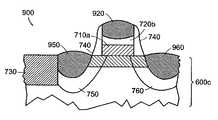
- the completed embodiment of a MOSFET 900is shown in FIG. 8B .
- FIG. 6illustrates an embodiment of a substrate 600 used as a base for fabrication of the embodiment of the MOSFET 900 .
- the substrate 600includes a relaxed SiGe layer 610 and a strained Si surface layer 640 .
- the substrate 600can provide a base for the fabrication of semiconductor devices, such as transistors.
- the substrate 600can be manufactured via epitaxial growth and polishing techniques, as described in commonly assigned U.S. Pat. No. 6,107,653 to Fitzgerald.
- the relaxed SiGe substrate layer 610can form the base substrate of many types of MOSFET devices.
- the thin strained Si layer 640can alternatively be a SiGe layer, a sequence of Si and SiGe layers, or other combination of thin epitaxial layers, as described above.
- FIGS. 7A–Billustrate some fabrication steps of a gate contact for the MOSFET 900 .
- FIG. 7Ashows a cross-sectional view of a device at a stage of fabrication, chronologically following the stage of FIG. 6 .
- regions of isolation portions 730have been formed in the substrate 600 to provide a modified substrate 600 a.
- a dielectric layer 710 and a polycrystalline semiconductor layer 720have been formed on the substrate 600 a.
- the polycrystalline semiconductor layer 720can include silicon and germanium.
- the isolation portion 730preferably is deep enough to cross all channel layers of semiconductor material in the substrate 600 a, ending at least in the SiGe relaxed layer of the substrate 600 a.
- the isolation portions 730are absent or replaced by other isolation means.
- one embodimentincludes semi-recessed oxide isolation (S-ROX) portions.
- S-ROXsemi-recessed oxide isolation
- a relatively high degree of planarityis preferably maintained between the upper surface of the substrate 600 a and the upper surface of the isolation portions 730 .
- the dielectric layer 710which provides a gate dielectric, is formed on the exposed surface of the substrate 600 , possibly consuming a portion of the surface of the strained-silicon layer 640 .
- the dielectric layer 710can be formed by various methods conventional in the art, e.g., via thermal oxidation of the surface of the substrate 600 or via a deposition technique.
- the dielectric layer 710can be, for example, a 15–100 ⁇ (1.5–10.0 nm) thick layer of silicon dioxide.
- Other embodimentsinclude other suitable dielectric materials, e.g., silicon oxynitride, silicon nitride, a plurality of silicon nitride and silicon oxide layers, or a high-k dielectric.
- a polycrystalline semiconductor layer 720is then deposited on the dielectric layer 710 , e.g., via chemical-vapor deposition.
- the polycrystalline semiconductor layer 720can be, for example, 1000 ⁇ (100 nm) thick.
- the polycrystalline semiconductor layer 720preferably has an upper portion including SiGe with a Ge content substantially identical to the Ge content of the relaxed SiGe layer 610 .
- a proximal (lower) portion of the layer 720has a different composition from that of the distal (upper) portion of the layer 720 .
- the composition of the distal portioncan be matched to the substrate layer 610 , while the portion in contact with the dielectric layer 710 can have a composition chosen, for example, for its compatibility with the dielectric material.
- polycrystalline siliconis highly compatible with silicon dioxide dielectric, the interface between these two materials has a relatively very low electrical defect density.
- FIG. 7Billustrates another stage in the production of the MOSFET 900 , related to some steps in the formation of a gate contact.
- the dielectric layer 710 and the polycrystalline semiconductor layer 720have been patterned to respectively form a gate dielectric 710 a and a gate contact semiconductor portion 720 a.
- the patterningcan be performed via methods conventional in the art, e.g., via photolithography and sputter etching.
- Contact sidewall spacers 740have been formed prior to formation of a source region 750 , and a drain region 760 .
- the sidewall spacers 740can provide isolation between the gate contact and source/drain regions 750 , 760 , and facilitate fabrication of self-aligned structures.
- the spacers 740can be formed via methods conventional in the art, e.g., via oxide deposition, thermal oxidation of polysilicon and/or nitride deposition.
- the source region 750 and the drain region 760include dopant, which extends across the interface between the silicon surface layer 640 and the SiGe relaxed layer in the further modified substrate 600 b.
- the structures illustrated in FIG. 7Bare fabricated as follows.
- a layer of photosensitive polymere.g., a Novolak-based photoresist, as known to one having ordinary skill in the semiconductor lithography arts
- the polymeris exposed and developed to define a photo-mask having substantially vertical sidewalls.
- the exposed portions of SiGe semiconductor layer 720are sequentially etched in a directional mode to define the gate contact semiconductor portion 720 a.
- the photo-maskis removed, e.g., via an O 2 plasma etch.
- the sidewall spacers 740are formed on the exposed sides of the gate contact semiconductor portion 720 a.
- the sidewall spacers 740can be formed using one of several known methods.
- a preferred methodis to deposit a layer of chemically vapor-deposited (CVD) oxide over the entire structure, and directionally etch the deposited layer so that it is removed from the horizontal surfaces of the substrate. During this removal step, exposed portions of the underlying dielectric layer 710 are also removed to define the gate dielectric 710 a.
- CVDchemically vapor-deposited
- the source region 750 and the drain region 760are defined, for example, through ion implantation and drive-in anneal.
- the diffusion regionscan be formed using one of several techniques. For example, implantation of dopant ions to define the diffusion regions can use the gate contact and isolation regions 730 as an implantation mask.
- FIGS. 8A–Billustrate aspects of silicide formation for the MOSFET 900 .
- FIG. 8Aillustrates deposition of a metal layer 820 on the structures illustrated in FIG. 7B .
- the metal layer 820is formed during a single deposition step, and is adjacent to portions of both the substrate 600 b and the gate contact semiconductor portion 720 a.
- the metal layer 820preferably is approximately 8–20 nanometers (nm) in thickness.
- FIG. 8Bis a cross-sectional view of the completed embodiment of the MOSFET 900 .
- the MOSFET 900includes a gate contact silicide 920 , source contact silicide 950 and a drain contact silicide 960 .
- the gate contact silicide 920forms from reaction of a portion of the metal layer 820 with SiGe in the gate contact semiconductor portion 720 a.
- the source and drain contacts 950 , 960form from reaction of a portion of the metal layer 820 with Si and SiGe in the substrate 600 b, thus leaving a further modified substrate 600 c.
- the metal layer 820reacts with SiGe having similar or identical compositions in both the gate contact and in the substrate 600 b, providing common silicidation behavior and silicide formation in a single step.
- an unreacted gate semiconductor portion 720 bcan remain in the contact.
- the gate contact semiconductor portion 720 aincludes SiGe with a graded composition.
- a distal portion of the gate contact semiconductor portion 720 ahas a composition that matches the relaxed SiGe layer 610 , and a proximal portion, adjacent to the gate dielectric 710 a, that has a greater Ge content.
- the greater Ge contentcan be substantially pure Ge.
- a proximal portion of the gate contact semiconductor portion 720 ais substantially pure silicon.
- This embodimentprovides single-step silicidation of source, drain and gate, as well as a high quality gate contact/gate oxide interface, for example when the gate oxide 710 a is a silicon dioxide. It can also provide, for example, a gate contact work function that is similar/identical to conventional MOSFETS.
Landscapes
- Engineering & Computer Science (AREA)
- Microelectronics & Electronic Packaging (AREA)
- Condensed Matter Physics & Semiconductors (AREA)
- General Physics & Mathematics (AREA)
- Manufacturing & Machinery (AREA)
- Computer Hardware Design (AREA)
- Physics & Mathematics (AREA)
- Power Engineering (AREA)
- Chemical & Material Sciences (AREA)
- Chemical Kinetics & Catalysis (AREA)
- Insulated Gate Type Field-Effect Transistor (AREA)
- Crystallography & Structural Chemistry (AREA)
- Electrodes Of Semiconductors (AREA)
Abstract
Description
This application is a divisional application of U.S. patent application Ser. No. 10/179,079, filed Jun. 25, 2002, now U.S. Pat. No. 6,982,474 the entire disclosure of which is incorporated by reference herein.
The invention generally relates to semiconductor devices, and, more particularly, to the fabrication and structure of contacts in transistors.
Continuous improvements in the fabrication and design of semiconductor transistors used in integrated circuit devices have permitted ever greater area densities of transistors. Development of materials and processing for interconnects and contacts plays a large role in transistor development.
Materials and processes for forming conductive contacts and interconnects must accommodate, for example, dimensional requirements, processing temperatures, reliability needs and materials compatibility. Traditional aluminum-based interconnects have gradually given way to copper interconnects for fine dimensions; cobalt silicide and other metallic materials are gradually supplanting titanium silicide source and drain contacts and titanium silicide caps on doped polycrystalline silicon gate contacts.
Another avenue for improvement in device performance involves the use of newer types of substrates as replacements for traditional silicon wafers. For example, wafers that have a silicon-germanium (SiGe) layer can provide improved channel layer performance in a strained-silicon layer grown on the SiGe layer.
Mobility enhancements obtained from strained silicon, in combination with source-drain and gate silicidation techniques, provide the opportunity to increase speed, reduce power consumption, and provide the basis of other advances in microelectronics, such as analog and digital device integration.
The use of substrates that include a SiGe layer, however, can increase fabrication complexity relative to that for conventional silicon wafer-based devices. For example, formation of source and drain contacts through reaction of a metal layer, such as titanium or cobalt, with SiGe in the substrate has preferred process conditions that are different from silicide formation with relatively pure silicon.
The invention involves structures and fabrication methods for semiconductor devices that preferably have semiconductor layers including two materials in both a substrate and in a gate contact. The invention provides simplified processing for semiconductor devices, as well as improved semiconductor device structures that include compound and/or alloyed semiconductors in both contacts and substrates. The invention provides for simultaneous reaction of a metal layer to form reacted material contacts in the substrate and a reacted material upper portion of a gate contact. The metal layer exhibits a similar reaction behavior with the semiconductor layers in both the substrate and in the upper portion of the gate contact due to a similar composition ratio of the two materials in both semiconductor layers.
Preferred embodiments of the invention feature substrates and contacts that include one or more semiconductor alloy layers of silicon and germanium. Preferred embodiments include SiGe layers of similar composition in both a substrate and a contact; conductive portions are formed by simultaneously reacting the SiGe layers in the substrate and the contact with a metal layer. Thus, for example, source and drain contacts in a substrate can be formed simultaneously with formation of a conductive upper (distal) portion of a gate contact having a portion that includes the semiconductor alloy. In this way, some processing steps are rendered unnecessary during basic device fabrication.
Simplified processing can be achieved in part because reaction of a metal layer with the substrate and with a semiconductor layer in a gate contact need not be decoupled to accommodate, for example, SiGe in the substrate and polycrystalline silicon in the gate. Proper material selection provides substrates and gate contacts that have similar or identical silicide formation steps. Other benefits can arise, such as lower temperature processing for silicide formation.
In preferred embodiments, the invention features transistors that include a gate electrode including SiGe in at least an upper portion of a gate contact (i.e., electrode) and a strained-silicon channel layer on a relaxed SiGe layer in a substrate. By having SiGe in an upper portion of a gate electrode, the silicidation of gate and source-drain regions can be performed in a single process. A lower portion of the gate contact can have a different material composition, chosen to provide, for example, a desired electrical property and/or compatibility with a gate dielectric material.
Thus, in a first aspect, the invention features a method for fabricating a semiconductor device. The method includes provision of a semiconductor layer that includes a first material and a second material. The semiconductor layer can be an alloy of two or more materials. The first and second materials can be silicon and germanium.
The semiconductor layer can be or include a relaxed layer. The relaxed layer can be part of a substrate having a portion, adjacent to the relaxed layer, with a lattice spacing mismatched to that of the relaxed layer. For example, the relaxed layer can be grown on intermediate layers that accommodate mismatch to a silicon wafer. As another example, the relaxed layer can reside on an oxide layer.
The method also includes the formation of a contact that has a portion proximal to the relaxed semiconductor layer and a portion distal to the relaxed semiconductor layer. The distal portion includes the first material and the second material. A metal layer is formed adjacent to the relaxed semiconductor layer and adjacent to the distal portion of the contact. The metal layer is simultaneously reacted with the relaxed semiconductor layer and with the distal portion of the contact.
The silicon and germanium of the distal portion of the contact can have an atomic density ratio that is substantially the same as an atomic density ratio of the silicon and germanium of the relaxed semiconductor layer. The proximal portion of the contact can consist essentially of silicon or essentially of germanium. Alternatively the proximal portion can include silicon and germanium, the atomic density ratio of the silicon and germanium of the proximal portion can differ from the atomic density ratio of the silicon and germanium of the distal portion.
In a second aspect, the invention features a semiconductor device. The device includes a substrate that has a reacted conductive layer that comprises silicon, germanium and a metallic material. The metallic material can be, e.g., titanium, nickel or cobalt. The device also includes a contact that has a portion proximal to the substrate and a reacted conductive portion distal to the substrate. The reacted conductive distal portion of the contact includes silicon, germanium and the same metallic material as in the substrate reacted conductive layer. The substrate can further include a strained semiconductor layer, for example, of silicon, adjacent to the contact.
In a third aspect, the invention features a semiconductor device that includes a substrate that has a reacted conductive layer comprising a first material, a second material and a metallic material. The device includes a contact having a portion proximal to the substrate and a reacted conductive portion distal to the substrate, the distal portion comprising the first material, the second material and the metallic material.
In the drawings, like reference characters generally refer to the same parts throughout the different views. Also, the drawings are not necessarily to scale, emphasis instead generally being placed upon illustrating the principles of the invention.
Various features of the invention are well suited to application in metal-oxide-semiconductor (MOS) transistors having Si, Si1−xGexand/or Ge layers in and or on a substrate. The invention provides means to avoid separation of metal layer reaction with the substrate and metal layer reaction with a polycrystalline silicon portion of a gate contact. The invention further provides improved gate design in conjunction with the advantages of a substrate that includes a SiGe layer, among other advantages.
The term “MOS” is here used to refer generally to semiconductor devices that include a conductive gate spaced at least by an insulting layer from a semiconducting channel layer. The terms “SiGe” and “Si1−xGex” are here used interchangeably to refer to silicon-germanium alloys. The term “silicide” is here used to refer to a reaction product of a metal, silicon, and optionally other components, such as germanium. The term “silicide” is also used, less formally, to refer to the reaction product of a metal with an elemental semiconductor, a compound semiconductor or an alloy semiconductor.
First, with reference toFIG. 1 , to provide a context for description of features of the invention, the structure and operation of a conventional MOSFET are described.FIG. 1 is cross-sectional view of a conventional silicon-based MOS field-effect transistor (MOSFET)100. Thetransistor 100 includes agate contact 120, a pair ofspacers 150, asource 135, asource silicide contact 130, agate oxide 126, adrain 145, adrain silicide contact 140 and asilicon substrate 110. Thetransistor 100 is electrically isolated from neighboring transistors by a shallow trench isolation (STI)portion 170.
Thegate contact 120 includes a doped, conductive polycrystalline silicon (“polysilicon”)portion 124 proximal to thegate oxide 126 and a distalgate silicide portion 122. Thesource 135 and drain145 include doped regions formed by implantation of dopant species into thesubstrate 110 and annealing, with thespacers 150 controlling the distribution of dopant beneath thegate oxide 126. Thesilicide contacts gate silicide portion 122 provide good ohmic interfaces respectively to thesource 135 and drain145 and to thegate polysilicon portion 124.
TheMOSFET 100 has a surface channel, which may be defined in physical or electrical terms. Physically, the surface channel is the p-type or n-type silicon that is adjacent to (i.e., below) thegate oxide 126 and which joins thesource 135 and drain145. Electrically, the channel is an inversion layer, which provides current flow between thesource 135 and drain145. Thus, from the electrical point of view, the presence and condition of the channel are variable.
TheMOSFET 200 includes a strained-silicon layer 220, asource 245, adrain 255, asource contact 240, adrain contact 250 and asubstrate 210 that includes a relaxed SiGe layer (other embodiments include a strained-SiGe layer). Thesilicon layer 220 can be epitaxially grown on thesubstrate 210, and provides a surface channel for theMOSFET 200. The source anddrain contacts substrate 210 and thesilicon layer 220. Thesource 245 and thedrain 255 can be formed by diffusing a dopant into thesubstrate 210silicon layer 220. The source anddrain contacts substrate 210, including, at least, portions of thesilicon layer 220 and the relaxed SiGe layer.
Referring now toFIGS. 3 and 4 , silicidation of silicon and SiGe are compared. Conventional processing methods would typically decouple the formation of the source anddrain contacts gate silicide portion 122 due to the differing silicidation behavior of SiGe in thesubstrate 210 and the polysilicon in the gate contact with a metal layer. As described below, with reference toFIGS. 3 and 4 , the silicide formation rate of silicon can be very different from the silicide formation rate of SiGe. WhileFIGS. 3 and 4 demonstrate differences in silicidation behavior between Si and SiGe after a single annealing step, it should be noted that silicidation processes can utilize multiple annealing steps, oftentimes with unreacted metal being stripped between anneals.
Point B indicates a desirable anneal temperature of 675° C. The sheet resistance of the reacted Si sample is more twice that of the reacted Si0.7Ge0.3sample for anneal times of approximately 2 minutes or less, again demonstrating the difference in the silicidation rates of Si and SiGe for desirable combinations of annealing time and temperature.
One method for overcoming the differences in silicidation rates of gate and source-drain regions is to decouple the gate silicide formation from the source-drain silicidation, as described in U.S. Pat. No. 4,755,478. The decoupled process for siliciding the source-drain regions and gate electrode regions of a SiGe substrate typically requires more processing steps due to separation of silicidation of polysilicon in a gate contact and silicidation of the source-drain contacts, each set of steps having different optimized conditions. Decoupling tends to increase the costs of the overall silicidation process.
The silicidation of Si can occur at a much higher temperature than silicidation of SiGe. Therefore, an optimized silicidation process involving a polysilicon gate can make the SiGe substrate layer vulnerable to, for example, interdiffusion, dislocation redistribution and silicide agglomeration. Features of the invention can remove a need for decoupling, and provide gate contacts and source/drain contacts with similar, optimized processing conditions. The invention can further provide processing at lower temperatures.
A channel layer, for example, of silicon, can be provided adjacent to the relaxed layer (Step530). For example, a surface channel silicon layer can be epitaxially grown on a SiGe relaxed layer. In some embodiments, a buried channel layer is provided adjacent to the relaxed layer. Some of these embodiments include one or more buried channel layers and a surface channel layer. The channel layers can include, for example Si, Ge or SiGe. The composition of a channel layer can be chosen in cooperation with the composition of a relaxed layer to provide a desired level of strain in the channel layer, as is conventional in the art.
Themethod 500 further includes formation of a contact adjacent to the relaxed layer (Step550). The contact includes a portion that is proximal to the relaxed semiconductor layer and a portion that is distal to the relaxed semiconductor layer, i.e., lower and upper portions. The distal portion includes the first material and the second material, and preferably has substantially the same composition as the relaxed semiconductor layer. Similar compositions, for example, of SiGe, in the relaxed layer and in the upper portion of the contact enable similar optimized processing conditions for reaction of a metal layer with the relaxed layer and with the upper portion of the contact. Thus, reaction of a metal layer can proceed simultaneously for the substrate and for the contact.
Formation of the contact can commence with formation of a lower portion that includes Si, Ge or SiGe (Step540). The distal portion can then be formed from SiGe having a different composition than the semiconductor of the proximal portion. The composition can vary abruptly or smoothly with position in the contact through the proximal and the distal portions. Thus, the composition of the proximal portion can be chosen, for example, for its electrical performance or compatibility with an adjacent gate dielectric, as described in below. The composition of the distal portion, in contrast, can be chosen to provide compatibility with the composition of the relaxed layer.
Themethod 500 further includes formation of a metal layer adjacent to the relaxed semiconductor layer and the distal portion of the contact (Step560). The metal can include, for example, titanium, cobalt, nickel, platinum, molybdenum, tungsten and/or zirconium. The metal layer is simultaneously reacted with the substrate and with the distal portion of the contact (Step570). In preferred embodiments, most of the metal layer that reacts with the substrate will react with the relaxed semiconductor layer, in part because any surface layers will be relatively thin. Thus, in these embodiments, the relaxed layer will dominate over other portions of the substrate in the reaction with the metal layer.
In the case of a substrate that includes a SiGe relaxed semiconductor layer, the above-described method permits the formation of source and drain silicide contacts in a substrate at the same time as formation of a distal germanium silicide portion of a gate contact. Both gate silicide and source and drain silicide can be formed under preferred time and temperature annealing conditions. Thus, rather than decoupling the formation of a conductive cap for the gate contact and formation of source and drain contacts, the invention facilitates simultaneous processing.
Various preferred embodiments of the invention utilize a substrate that includes a SiGe layer. The SiGe layer can be grown on a silicon wafer, and can include more than one layer of alloys of varying composition, thickness and growth conditions. Thus, the substrate can include a SiGe layer or multiple SiGe layers and/or SiGe layers having graded composition. In some embodiments, the SiGe layer includes a relaxed SiGe layer grown on intermediate SiGe layers that accommodate the lattice mismatch with a silicon wafer.
The substrate can include, for example, a silicon wafer, with the SiGe layers grown on the silicon wafer. In this case, an oxide layer can be present between the silicon wafer and the SiGe layer. Other types of wafers can be used as a base for a substrate, e.g., silicon-on-insulator (SOI) wafers, germanium wafers, glass substrates and laminated substrates.
A channel layer can be a surface or a buried layer, and can be formed, for example, from silicon, germanium or a combination of silicon and germanium. For example, a buried channel layer can be a strained silicon layer epitaxially grown on a relaxed SiGe layer. Alternatively, the buried layer, can be germanium or can be SiGe having a composition that is different from the SiGe of the relaxed layer.
For example, the buried channel layer can have a composition of Si1−xGexwhile the relaxed layer has a composition of Si1−yGey. For x>y, the buried SiGe layer is under compressive stress, and thus exhibits a compressive strain. Thus, material combinations can be chosen to provide a p-channel MOSFET, preferably by provding a compressively strained SiGe buried layer, or an n-channel MOSFET, preferable by providing a tensilely strained silicon layer.
Some preferred embodiments of the invention use relaxed SiGe layers grown on silicon substrates. Silicon, germanium and SiGe layers can be grown via known epitaxial growth techniques. Growth of a buried layer of silicon, germanium or SiGe on a SiGe relaxed layer, or SiGe on silicon, enables production of buried layers of controlled stress and dislocation density. Examples of SiGe substrates, in which the Ge content can be up to 100%, include: a relaxed, uniform composition SiGe layer on a graded composition SiGe layer atop a Si substrate; a relaxed, uniform composition SiGe layer directly adjacent to a Si substrate; and a relaxed, uniform composition SiGe layer on an insulating layer like SiO2, adjacent a Si substrate.
Referring now toFIGS. 6–8 , steps in an embodiment of a MOSFET fabrication process, and some preferred device structures, are described.FIGS. 6–8 are chronologically arranged cross-sectional views of MOSFET-related structures at various stages of an embodiment of a MOSFET fabrication process. The completed embodiment of aMOSFET 900 is shown inFIG. 8B .
It will be appreciated by those skilled in the art that the relaxedSiGe substrate layer 610 can form the base substrate of many types of MOSFET devices. The thinstrained Si layer 640 can alternatively be a SiGe layer, a sequence of Si and SiGe layers, or other combination of thin epitaxial layers, as described above.
Theisolation portion 730 preferably is deep enough to cross all channel layers of semiconductor material in thesubstrate 600a,ending at least in the SiGe relaxed layer of thesubstrate 600a.In other embodiments, theisolation portions 730 are absent or replaced by other isolation means. For example, one embodiment includes semi-recessed oxide isolation (S-ROX) portions. Generally, a relatively high degree of planarity is preferably maintained between the upper surface of thesubstrate 600aand the upper surface of theisolation portions 730.
Thedielectric layer 710, which provides a gate dielectric, is formed on the exposed surface of thesubstrate 600, possibly consuming a portion of the surface of the strained-silicon layer 640. Thedielectric layer 710 can be formed by various methods conventional in the art, e.g., via thermal oxidation of the surface of thesubstrate 600 or via a deposition technique.
Thedielectric layer 710 can be, for example, a 15–100 Å (1.5–10.0 nm) thick layer of silicon dioxide. Other embodiments include other suitable dielectric materials, e.g., silicon oxynitride, silicon nitride, a plurality of silicon nitride and silicon oxide layers, or a high-k dielectric.
Apolycrystalline semiconductor layer 720 is then deposited on thedielectric layer 710, e.g., via chemical-vapor deposition. Thepolycrystalline semiconductor layer 720 can be, for example, 1000 Å (100 nm) thick.
Thepolycrystalline semiconductor layer 720 preferably has an upper portion including SiGe with a Ge content substantially identical to the Ge content of therelaxed SiGe layer 610. In some embodiments, a proximal (lower) portion of thelayer 720 has a different composition from that of the distal (upper) portion of thelayer 720. Thus, the composition of the distal portion can be matched to thesubstrate layer 610, while the portion in contact with thedielectric layer 710 can have a composition chosen, for example, for its compatibility with the dielectric material. For example, polycrystalline silicon is highly compatible with silicon dioxide dielectric, the interface between these two materials has a relatively very low electrical defect density.
Contactsidewall spacers 740 have been formed prior to formation of asource region 750, and adrain region 760. The sidewall spacers740 can provide isolation between the gate contact and source/drain regions spacers 740 can be formed via methods conventional in the art, e.g., via oxide deposition, thermal oxidation of polysilicon and/or nitride deposition.
Thesource region 750 and thedrain region 760 include dopant, which extends across the interface between thesilicon surface layer 640 and the SiGe relaxed layer in the further modifiedsubstrate 600b.
For one embodiment of theMOSFET 900, the structures illustrated inFIG. 7B are fabricated as follows. A layer of photosensitive polymer (e.g., a Novolak-based photoresist, as known to one having ordinary skill in the semiconductor lithography arts) is coated on a polycrystalline-SiGe semiconductor layer 720. The polymer is exposed and developed to define a photo-mask having substantially vertical sidewalls. The exposed portions ofSiGe semiconductor layer 720 are sequentially etched in a directional mode to define the gatecontact semiconductor portion 720a.The photo-mask is removed, e.g., via an O2plasma etch.
The sidewall spacers740 are formed on the exposed sides of the gatecontact semiconductor portion 720a.The sidewall spacers740 can be formed using one of several known methods. A preferred method is to deposit a layer of chemically vapor-deposited (CVD) oxide over the entire structure, and directionally etch the deposited layer so that it is removed from the horizontal surfaces of the substrate. During this removal step, exposed portions of theunderlying dielectric layer 710 are also removed to define the gate dielectric710a.
After thesidewall spacers 740 are formed, thesource region 750 and thedrain region 760 are defined, for example, through ion implantation and drive-in anneal. The diffusion regions can be formed using one of several techniques. For example, implantation of dopant ions to define the diffusion regions can use the gate contact andisolation regions 730 as an implantation mask.
Thegate contact silicide 920, forms from reaction of a portion of themetal layer 820 with SiGe in the gatecontact semiconductor portion 720a.The source anddrain contacts metal layer 820 with Si and SiGe in thesubstrate 600b,thus leaving a further modifiedsubstrate 600c.Themetal layer 820 reacts with SiGe having similar or identical compositions in both the gate contact and in thesubstrate 600b,providing common silicidation behavior and silicide formation in a single step.
After reaction of themetal layer 820 with neighboring material, an unreactedgate semiconductor portion 720bcan remain in the contact. Some metals that can be used in themetal layer 820 are described in the following:
- Titanium—can provide a good silicide on SiGe, but generally not well suited to short gate length polysilicon gates.
- Cobalt—generally preferable relative to Ti for sub-quarter micrometer linewidths, but can lead to agglomeration problems in conjunction with SiGe having a Ge atomic fraction of greater than approximately 15%.
- Nickel—generally works well with SiGe, at least for Ge atomic compositions of up to 45–50% or more, and consumes less silicon during silicidation than some other metals.
- Platinum—generally works well with SiGe, at least for Ge atomic compositions of up to 45–50% or more.
- Zirconium—can be used with SiGe.
- Multilayered metals—stacked metal layers (e.g., Pt/Ni) can be used.
- Alloys—can be used (e.g., NiPt).
In one embodiment of theMOSFET 900, the gatecontact semiconductor portion 720aincludes SiGe with a graded composition. In this embodiment, a distal portion of the gatecontact semiconductor portion 720ahas a composition that matches therelaxed SiGe layer 610, and a proximal portion, adjacent to the gate dielectric710a,that has a greater Ge content. The greater Ge content can be substantially pure Ge. This embodiment provides single-step silicidation of source, drain and gate with the further advantage of an improved work function due to the elevated Ge content at the interface with the gate dielectric710a.
In another embodiment, a proximal portion of the gatecontact semiconductor portion 720ais substantially pure silicon. This embodiment provides single-step silicidation of source, drain and gate, as well as a high quality gate contact/gate oxide interface, for example when thegate oxide 710ais a silicon dioxide. It can also provide, for example, a gate contact work function that is similar/identical to conventional MOSFETS.
Variations, modifications, and other implementations of what is described herein will occur to those of ordinary skill in the art without departing from the spirit and the scope of the invention as claimed. Accordingly, the invention is to be defined not by the preceding illustrative description but instead by the spirit and scope of the following claims.
Claims (42)
1. A method for forming a semiconductor device, the method comprising:
providing a substrate;
forming a gate dielectric layer over a portion of the substrate, thereby defining a channel below the gate dielectric layer;
forming a source contact and a drain contact proximate the channel by depositing a metallic material and performing an annealing step, each of the source contact and drain contact comprising a reacted conductive silicide layer, the reacted conductive silicide layer comprising silicon, germanium, and the metallic material; and
forming a gate contact over at least a portion of the gate dielectric layer by depositing the metallic material and performing an annealing step, the gate contact including a reacted conductive silicide portion comprising a semiconductor material and the metallic material,
wherein the channel of the semiconductor device is strained.
2. The method ofclaim 1 , wherein the reacted conductive silicide layer of at least one of the source contact and drain contact is formed proximate a material comprising SiGe.
3. The method ofclaim 2 , further comprising defining an isolation region proximate the material comprising SiGe.
4. The method ofclaim 2 , wherein the SiGe is at least partially relaxed.
5. The method ofclaim 1 , wherein the reacted conductive silicide portion of the gate contact comprises germanium.
6. The method ofclaim 1 , wherein the gate contact comprises an unreacted semiconductor portion.
7. The method ofclaim 6 , wherein the unreacted semiconductor portion consists essentially of polycrystalline silicon.
8. The method ofclaim 6 , wherein the unreacted semiconductor portion comprises germanium.
9. The method ofclaim 1 , further comprising forming a strain-inducing material over at least a portion of the substrate, the strain-inducing material comprising silicon, wherein strain in the strained channel is induced by the strain-inducing material.
10. The method ofclaim 9 , wherein forming the strain-inducing material comprises epitaxial growth.
11. The method ofclaim 9 , further comprising defining an isolation region, wherein the isolation region is disposed proximate the strain-inducing material.
12. The method ofclaim 1 , further comprising forming a strain-inducing material over at least a portion of the substrate, the strain-inducing material comprising germanium, wherein strain in the strained channel is induced by the strain-inducing material.
13. The method ofclaim 12 , wherein forming the strain-inducing material comprises epitaxial growth.
14. The method ofclaim 12 , further comprising defining an isolation region, wherein the isolation region is disposed proximate the strain-inducing material.
15. The method ofclaim 12 , wherein the strain-inducing material is at least partially relaxed.
16. The method ofclaim 1 , wherein the metallic material comprises at least one of nickel, platinum, and zirconium.
17. The method ofclaim 1 , wherein the strained channel comprises at least one of silicon and germanium.
18. The method ofclaim 1 , wherein the strained channel is disposed proximate a material comprising SiGe.
19. The method ofclaim 1 , wherein the strained channel is tensilely strained.
20. The method ofclaim 1 , wherein the strained channel is compressively strained.
21. The method ofclaim 1 , wherein the gate dielectric layer comprises at least one of silicon oxynitride and a high-k dielectric.
22. The method ofclaim 1 , wherein forming the gate dielectric layer comprises at least one of oxidation and deposition.
23. The method ofclaim 1 , wherein the strained channel is disposed over an insulator layer.
24. The method ofclaim 1 , wherein the strained channel is disposed over a relaxed material.
25. The method ofclaim 16 , wherein the metallic material comprises nickel.
26. The method ofclaim 25 , wherein the metallic material consists essentially of nickel.
27. The method ofclaim 26 , wherein the strained channel comprises silicon.
28. The method ofclaim 27 , wherein the strained channel is compressively strained.
29. The method ofclaim 27 , wherein the strained channel consists essentially of silicon.
30. The method ofclaim 29 , wherein the strained channel is compressively strained.
31. The method ofclaim 29 , further comprising forming a strain-inducing material over at least a portion of the substrate, the strain-inducing material consisting essentially of SiGe, wherein strain in the strained channel is induced by the strain-inducing material.
32. The method ofclaim 31 , wherein the strain-inducing material is disposed proximate the reacted conductive silicide layer and the strained channel.
33. The method ofclaim 32 , wherein forming the strain-inducing material comprises epitaxial growth.
34. The method ofclaim 33 , wherein the substrate consists essentially of one or more semiconductor materials.
35. The method ofclaim 34 , wherein the substrate consists essentially of silicon.
36. The method ofclaim 35 , further comprising defining an isolation region, wherein the strain-inducing material is disposed proximate the isolation region.
37. The method ofclaim 36 , wherein the semiconductor device is a p-channel MOSFET.
38. The method ofclaim 37 , wherein the strained channel is compressively strained.
39. The method ofclaim 33 , wherein the strained channel is disposed over an insulator layer.
40. The method ofclaim 39 , further comprising defining an isolation region, wherein the strain-inducing material is disposed proximate the isolation region.
41. The method ofclaim 40 , wherein the semiconductor device is a p-channel MOSFET.
42. The method ofclaim 41 , wherein the strained channel is compressively strained.
Priority Applications (1)
| Application Number | Priority Date | Filing Date | Title |
|---|---|---|---|
| US11/073,976US7217603B2 (en) | 2002-06-25 | 2005-03-07 | Methods of forming reacted conductive gate electrodes |
Applications Claiming Priority (2)
| Application Number | Priority Date | Filing Date | Title |
|---|---|---|---|
| US10/179,079US6982474B2 (en) | 2002-06-25 | 2002-06-25 | Reacted conductive gate electrodes |
| US11/073,976US7217603B2 (en) | 2002-06-25 | 2005-03-07 | Methods of forming reacted conductive gate electrodes |
Related Parent Applications (1)
| Application Number | Title | Priority Date | Filing Date |
|---|---|---|---|
| US10/179,079DivisionUS6982474B2 (en) | 2002-06-25 | 2002-06-25 | Reacted conductive gate electrodes |
Publications (2)
| Publication Number | Publication Date |
|---|---|
| US20050156210A1 US20050156210A1 (en) | 2005-07-21 |
| US7217603B2true US7217603B2 (en) | 2007-05-15 |
Family
ID=29734849
Family Applications (8)
| Application Number | Title | Priority Date | Filing Date |
|---|---|---|---|
| US10/179,079Expired - LifetimeUS6982474B2 (en) | 2002-06-25 | 2002-06-25 | Reacted conductive gate electrodes |
| US10/944,618Expired - Fee RelatedUS8129821B2 (en) | 2002-06-25 | 2004-09-17 | Reacted conductive gate electrodes |
| US11/073,976Expired - LifetimeUS7217603B2 (en) | 2002-06-25 | 2005-03-07 | Methods of forming reacted conductive gate electrodes |
| US13/342,589Expired - LifetimeUS8785315B2 (en) | 2002-06-25 | 2012-01-03 | Reacted conductive gate electrodes and methods of making the same |
| US14/320,065Expired - Fee RelatedUS9048167B2 (en) | 2002-06-25 | 2014-06-30 | Reacted conductive gate electrodes and methods of making the same |
| US14/697,337Expired - LifetimeUS9343539B2 (en) | 2002-06-25 | 2015-04-27 | Reacted conductive gate electrodes and methods of making the same |
| US15/137,517Expired - LifetimeUS9812572B2 (en) | 2002-06-25 | 2016-04-25 | Reacted conductive gate electrodes and methods of making the same |
| US15/784,925Expired - Fee RelatedUS10629735B2 (en) | 2002-06-25 | 2017-10-16 | Reacted conductive gate electrodes and methods of making the same |
Family Applications Before (2)
| Application Number | Title | Priority Date | Filing Date |
|---|---|---|---|
| US10/179,079Expired - LifetimeUS6982474B2 (en) | 2002-06-25 | 2002-06-25 | Reacted conductive gate electrodes |
| US10/944,618Expired - Fee RelatedUS8129821B2 (en) | 2002-06-25 | 2004-09-17 | Reacted conductive gate electrodes |
Family Applications After (5)
| Application Number | Title | Priority Date | Filing Date |
|---|---|---|---|
| US13/342,589Expired - LifetimeUS8785315B2 (en) | 2002-06-25 | 2012-01-03 | Reacted conductive gate electrodes and methods of making the same |
| US14/320,065Expired - Fee RelatedUS9048167B2 (en) | 2002-06-25 | 2014-06-30 | Reacted conductive gate electrodes and methods of making the same |
| US14/697,337Expired - LifetimeUS9343539B2 (en) | 2002-06-25 | 2015-04-27 | Reacted conductive gate electrodes and methods of making the same |
| US15/137,517Expired - LifetimeUS9812572B2 (en) | 2002-06-25 | 2016-04-25 | Reacted conductive gate electrodes and methods of making the same |
| US15/784,925Expired - Fee RelatedUS10629735B2 (en) | 2002-06-25 | 2017-10-16 | Reacted conductive gate electrodes and methods of making the same |
Country Status (3)
| Country | Link |
|---|---|
| US (8) | US6982474B2 (en) |
| AU (1) | AU2003278428A1 (en) |
| WO (1) | WO2004001825A1 (en) |
Cited By (19)
| Publication number | Priority date | Publication date | Assignee | Title |
|---|---|---|---|---|
| US20050158923A1 (en)* | 2003-08-28 | 2005-07-21 | Chun-Chieh Lin | Ultra-thin body transistor with recessed silicide contacts |
| US20050156255A1 (en)* | 2004-01-21 | 2005-07-21 | Taiwan Semiconductor Manufacturing Co. | Noble high-k device |
| US20070108481A1 (en)* | 2005-11-14 | 2007-05-17 | Freescale Semiconductor, Inc. | Electronic devices including a semiconductor layer and a process for forming the same |
| US20070278583A1 (en)* | 2006-06-01 | 2007-12-06 | International Business Machines Corporation | Gate stress engineering for mosfet |
| US20080135873A1 (en)* | 2006-12-08 | 2008-06-12 | Amberwave Systems Corporation | Inducement of Strain in a Semiconductor Layer |
| US20080211000A1 (en)* | 2007-03-01 | 2008-09-04 | Nec Electronics Corporation | Semiconductor device having transistors each having gate electrode of different metal ratio and production process thereof |
| US20090072325A1 (en)* | 2007-01-31 | 2009-03-19 | Chih-Chiang Wu | Metal-oxide semiconductor transistor |
| US20090176343A1 (en)* | 2005-03-09 | 2009-07-09 | Fujitsu Microelectronics Limited | P-channel MOS transistor and fabrication process thereof |
| US20090179251A1 (en)* | 2008-01-11 | 2009-07-16 | International Business Machines Corporation | Device and design structures for memory cells in a non-volatile random access memory and methods of fabricating such device structures |
| US20090179268A1 (en)* | 2008-01-11 | 2009-07-16 | International Business Machines Corporation | Design structures for high-voltage integrated circuits |
| US20090179266A1 (en)* | 2008-01-11 | 2009-07-16 | International Business Machines Corporation | Device structures for a metal-oxide-semiconductor field effect transistor and methods of fabricating such device structures |
| US20090179267A1 (en)* | 2008-01-11 | 2009-07-16 | International Business Machines Corporation | Semiconductor-on-insulator high-voltage device structures, methods of fabricating such device structures, and design structures for high-voltage circuits |
| US20090230427A1 (en)* | 2008-03-13 | 2009-09-17 | International Business Machines Corporation | Semiconductor devices having tensile and/or compressive stress and methods of manufacturing |
| US20100044762A1 (en)* | 2006-06-30 | 2010-02-25 | Freescale Semiconductor, Inc. | Method for forming a semiconductor device and structure thereof |
| US20100181626A1 (en)* | 2009-01-21 | 2010-07-22 | Jing-Cheng Lin | Methods for Forming NMOS and PMOS Devices on Germanium-Based Substrates |
| US20100197084A1 (en)* | 2009-02-04 | 2010-08-05 | Hynix Semiconductor Inc. | Method for manufacturing semiconductor device |
| US8927378B2 (en) | 2010-11-11 | 2015-01-06 | International Business Machines Corporation | Trench silicide contact with low interface resistance |
| US10985076B2 (en) | 2018-08-24 | 2021-04-20 | International Business Machines Corporation | Single metallization scheme for gate, source, and drain contact integration |
| US20230261092A1 (en)* | 2022-02-14 | 2023-08-17 | United Microelectronics Corp. | Middle voltage transistor and fabricating method of the same |
Families Citing this family (31)
| Publication number | Priority date | Publication date | Assignee | Title |
|---|---|---|---|---|
| US6649480B2 (en)* | 2000-12-04 | 2003-11-18 | Amberwave Systems Corporation | Method of fabricating CMOS inverter and integrated circuits utilizing strained silicon surface channel MOSFETs |
| US6830976B2 (en) | 2001-03-02 | 2004-12-14 | Amberwave Systems Corproation | Relaxed silicon germanium platform for high speed CMOS electronics and high speed analog circuits |
| US6703688B1 (en)* | 2001-03-02 | 2004-03-09 | Amberwave Systems Corporation | Relaxed silicon germanium platform for high speed CMOS electronics and high speed analog circuits |
| US6995430B2 (en)* | 2002-06-07 | 2006-02-07 | Amberwave Systems Corporation | Strained-semiconductor-on-insulator device structures |
| US6946371B2 (en)* | 2002-06-10 | 2005-09-20 | Amberwave Systems Corporation | Methods of fabricating semiconductor structures having epitaxially grown source and drain elements |
| US6982474B2 (en) | 2002-06-25 | 2006-01-03 | Amberwave Systems Corporation | Reacted conductive gate electrodes |
| JP3597831B2 (en)* | 2002-07-01 | 2004-12-08 | 株式会社東芝 | Field effect transistor and method of manufacturing the same |
| US6756276B1 (en)* | 2002-09-30 | 2004-06-29 | Advanced Micro Devices, Inc. | Strained silicon MOSFET having improved source/drain extension dopant diffusion resistance and method for its fabrication |
| WO2004081982A2 (en)* | 2003-03-07 | 2004-09-23 | Amberwave Systems Corporation | Shallow trench isolation process |
| JP2005005510A (en)* | 2003-06-12 | 2005-01-06 | Toshiba Corp | Semiconductor device and manufacturing method thereof |
| US7256465B2 (en)* | 2004-01-21 | 2007-08-14 | Sharp Laboratories Of America, Inc. | Ultra-shallow metal oxide surface channel MOS transistor |
| US7449782B2 (en)* | 2004-05-04 | 2008-11-11 | International Business Machines Corporation | Self-aligned metal to form contacts to Ge containing substrates and structure formed thereby |
| US7150516B2 (en) | 2004-09-28 | 2006-12-19 | Hewlett-Packard Development Company, L.P. | Integrated circuit and method for manufacturing |
| US7892905B2 (en)* | 2005-08-02 | 2011-02-22 | Globalfoundries Singapore Pte. Ltd. | Formation of strained Si channel and Si1-xGex source/drain structures using laser annealing |
| TW200725707A (en)* | 2005-12-30 | 2007-07-01 | Ind Tech Res Inst | Method for forming titanium silicide upon a semiconductor device with lower source/drain sheet resistance |
| US7544584B2 (en)* | 2006-02-16 | 2009-06-09 | Micron Technology, Inc. | Localized compressive strained semiconductor |
| US7795661B2 (en)* | 2006-03-07 | 2010-09-14 | International Business Machines Corporation | Vertical SOI transistor memory cell |
| US7618891B2 (en)* | 2006-05-01 | 2009-11-17 | International Business Machines Corporation | Method for forming self-aligned metal silicide contacts |
| US7485544B2 (en)* | 2006-08-02 | 2009-02-03 | Micron Technology, Inc. | Strained semiconductor, devices and systems and methods of formation |
| US8962447B2 (en)* | 2006-08-03 | 2015-02-24 | Micron Technology, Inc. | Bonded strained semiconductor with a desired surface orientation and conductance direction |
| US7968960B2 (en) | 2006-08-18 | 2011-06-28 | Micron Technology, Inc. | Methods of forming strained semiconductor channels |
| US7800182B2 (en)* | 2006-11-20 | 2010-09-21 | Infineon Technologies Ag | Semiconductor devices having pFET with SiGe gate electrode and embedded SiGe source/drain regions and methods of making the same |
| US9379011B2 (en)* | 2008-12-19 | 2016-06-28 | Asm International N.V. | Methods for depositing nickel films and for making nickel silicide and nickel germanide |
| CN102468164B (en) | 2010-10-29 | 2014-10-08 | 中国科学院微电子研究所 | Transistor and method of manufacturing the same |
| US8288758B2 (en) | 2010-12-02 | 2012-10-16 | International Business Machines Corporation | SOI SiGe-base lateral bipolar junction transistor |
| FR2989517B1 (en)* | 2012-04-12 | 2015-01-16 | Commissariat Energie Atomique | RESUME OF CONTACT ON HETEROGENE SEMICONDUCTOR SUBSTRATE |
| CN103489777A (en)* | 2012-06-11 | 2014-01-01 | 中芯国际集成电路制造(上海)有限公司 | Stress memory technology method |
| US9978868B2 (en)* | 2015-11-16 | 2018-05-22 | Taiwan Semiconductor Manufacturing Co., Ltd. | Negative capacitance field effect transistor with charged dielectric material |
| US10978548B2 (en)* | 2016-11-10 | 2021-04-13 | Texas Instruments Incorporated | Integrated capacitor with sidewall having reduced roughness |
| US10438999B2 (en)* | 2017-12-29 | 2019-10-08 | Spin Memory, Inc. | Annular vertical Si etched channel MOS devices |
| US11502106B2 (en)* | 2020-02-11 | 2022-11-15 | Globalfoundries U.S. Inc. | Multi-layered substrates of semiconductor devices |
Citations (322)
| Publication number | Priority date | Publication date | Assignee | Title |
|---|---|---|---|---|
| US4010045A (en) | 1973-12-13 | 1977-03-01 | Ruehrwein Robert A | Process for production of III-V compound crystals |
| US4522662A (en) | 1983-08-12 | 1985-06-11 | Hewlett-Packard Company | CVD lateral epitaxial growth of silicon over insulators |
| JPS61141116U (en) | 1985-02-22 | 1986-09-01 | ||
| US4710788A (en) | 1985-11-30 | 1987-12-01 | Licentia Patent-Verwaltungs-Gmbh | Modulation doped field effect transistor with doped Six Ge1-x -intrinsic Si layering |
| US4717681A (en) | 1986-05-19 | 1988-01-05 | Texas Instruments Incorporated | Method of making a heterojunction bipolar transistor with SIPOS |
| US4749441A (en) | 1986-12-11 | 1988-06-07 | General Motors Corporation | Semiconductor mushroom structure fabrication |
| US4755478A (en) | 1987-08-13 | 1988-07-05 | International Business Machines Corporation | Method of forming metal-strapped polysilicon gate electrode for FET device |
| US4786615A (en) | 1987-08-31 | 1988-11-22 | Motorola Inc. | Method for improved surface planarity in selective epitaxial silicon |
| US4803539A (en) | 1985-03-29 | 1989-02-07 | International Business Machines Corporation | Dopant control of metal silicide formation |
| JPH02210816A (en) | 1989-02-10 | 1990-08-22 | Fujitsu Ltd | Compound semiconductor lamination body |
| US4963506A (en) | 1989-04-24 | 1990-10-16 | Motorola Inc. | Selective deposition of amorphous and polycrystalline silicon |
| US4969031A (en) | 1982-02-03 | 1990-11-06 | Hitachi, Ltd. | Semiconductor devices and method for making the same |
| US4987462A (en) | 1987-01-06 | 1991-01-22 | Texas Instruments Incorporated | Power MISFET |
| US4990979A (en) | 1988-05-13 | 1991-02-05 | Eurosil Electronic Gmbh | Non-volatile memory cell |
| US4997776A (en) | 1989-03-06 | 1991-03-05 | International Business Machines Corp. | Complementary bipolar transistor structure and method for manufacture |
| US5013681A (en) | 1989-09-29 | 1991-05-07 | The United States Of America As Represented By The Secretary Of The Navy | Method of producing a thin silicon-on-insulator layer |
| US5034348A (en) | 1990-08-16 | 1991-07-23 | International Business Machines Corp. | Process for forming refractory metal silicide layers of different thicknesses in an integrated circuit |
| US5089872A (en) | 1990-04-27 | 1992-02-18 | North Carolina State University | Selective germanium deposition on silicon and resulting structures |
| US5091767A (en) | 1991-03-18 | 1992-02-25 | At&T Bell Laboratories | Article comprising a lattice-mismatched semiconductor heterostructure |
| US5108946A (en) | 1989-05-19 | 1992-04-28 | Motorola, Inc. | Method of forming planar isolation regions |
| DE4101167A1 (en) | 1991-01-17 | 1992-07-23 | Daimler Benz Ag | ARRANGEMENT AND METHOD FOR PRODUCING COMPLEMENTARY FIELD EFFECT TRANSISTORS |
| US5155571A (en) | 1990-08-06 | 1992-10-13 | The Regents Of The University Of California | Complementary field effect transistors having strained superlattice structure |
| JPH04307974A (en) | 1991-04-05 | 1992-10-30 | Sharp Corp | Electrically erasable nonvolatile semiconductor memory device |
| EP0514018A2 (en) | 1991-04-24 | 1992-11-19 | AT&T Corp. | Method for making low defect density semiconductor heterostructure and devices made thereby |
| US5166084A (en) | 1991-09-03 | 1992-11-24 | Motorola, Inc. | Process for fabricating a silicon on insulator field effect transistor |
| JPH0474415B2 (en) | 1983-08-26 | 1992-11-26 | ||
| US5177583A (en) | 1990-02-20 | 1993-01-05 | Kabushiki Kaisha Toshiba | Heterojunction bipolar transistor |
| US5198689A (en) | 1988-11-30 | 1993-03-30 | Fujitsu Limited | Heterojunction bipolar transistor |
| US5202284A (en) | 1989-12-01 | 1993-04-13 | Hewlett-Packard Company | Selective and non-selective deposition of Si1-x Gex on a Si subsrate that is partially masked with SiO2 |
| US5208182A (en) | 1991-11-12 | 1993-05-04 | Kopin Corporation | Dislocation density reduction in gallium arsenide on silicon heterostructures |
| US5207864A (en) | 1991-12-30 | 1993-05-04 | Bell Communications Research | Low-temperature fusion of dissimilar semiconductors |
| US5212112A (en) | 1991-05-23 | 1993-05-18 | At&T Bell Laboratories | Selective epitaxy of silicon in silicon dioxide apertures with suppression of unwanted formation of facets |
| US5212110A (en) | 1992-05-26 | 1993-05-18 | Motorola, Inc. | Method for forming isolation regions in a semiconductor device |
| US5217923A (en) | 1989-02-13 | 1993-06-08 | Kabushiki Kaisha Toshiba | Method of fabricating a semiconductor device having silicided source/drain regions |
| JPH05166724A (en) | 1991-12-19 | 1993-07-02 | Fujitsu Ltd | Silicon substrate compound semiconductor device and its manufacture |
| US5225703A (en) | 1990-06-11 | 1993-07-06 | Mitsubishi Denki Kabushiki Kaisha | Dual field effect transistor structure employing a single source region |
| US5241197A (en) | 1989-01-25 | 1993-08-31 | Hitachi, Ltd. | Transistor provided with strained germanium layer |
| US5240876A (en) | 1991-02-22 | 1993-08-31 | Harris Corporation | Method of fabricating SOI wafer with SiGe as an etchback film in a BESOI process |
| US5243207A (en) | 1991-03-15 | 1993-09-07 | Texas Instruments Incorporated | Method to integrate HBTs and FETs |
| US5242847A (en) | 1992-07-27 | 1993-09-07 | North Carolina State University At Raleigh | Selective deposition of doped silion-germanium alloy on semiconductor substrate |
| US5250445A (en) | 1988-12-20 | 1993-10-05 | Texas Instruments Incorporated | Discretionary gettering of semiconductor circuits |
| US5285086A (en) | 1990-08-02 | 1994-02-08 | At&T Bell Laboratories | Semiconductor devices with low dislocation defects |
| US5291439A (en) | 1991-09-12 | 1994-03-01 | International Business Machines Corporation | Semiconductor memory cell and memory array with inversion layer |
| US5294564A (en) | 1989-03-31 | 1994-03-15 | Thomson-Csf | Method for the directed modulation of the composition or doping of semiconductors, notably for the making of planar type monolithic electronic components, use of the method and corresponding products |
| US5298452A (en) | 1986-09-12 | 1994-03-29 | International Business Machines Corporation | Method and apparatus for low temperature, low pressure chemical vapor deposition of epitaxial silicon layers |
| US5310451A (en) | 1993-08-19 | 1994-05-10 | International Business Machines Corporation | Method of forming an ultra-uniform silicon-on-insulator layer |
| US5316958A (en) | 1990-05-31 | 1994-05-31 | International Business Machines Corporation | Method of dopant enhancement in an epitaxial silicon layer by using germanium |
| JPH06177046A (en) | 1992-06-04 | 1994-06-24 | Fujitsu Ltd | Hetero-epitaxial growth method |
| US5334861A (en) | 1992-05-19 | 1994-08-02 | Motorola Inc. | Semiconductor memory cell |
| JPH06244112A (en) | 1993-02-16 | 1994-09-02 | Fujitsu Ltd | Method of growing compound semiconductor crystal |
| US5346848A (en) | 1993-06-01 | 1994-09-13 | Motorola, Inc. | Method of bonding silicon and III-V semiconductor materials |
| US5374564A (en) | 1991-09-18 | 1994-12-20 | Commissariat A L'energie Atomique | Process for the production of thin semiconductor material films |
| US5413679A (en) | 1993-06-30 | 1995-05-09 | The United States Of America As Represented By The Secretary Of The Navy | Method of producing a silicon membrane using a silicon alloy etch stop layer |
| US5424243A (en) | 1993-09-20 | 1995-06-13 | Fujitsu Limited | Method of making a compound semiconductor crystal-on-substrate structure |
| US5426069A (en) | 1992-04-09 | 1995-06-20 | Dalsa Inc. | Method for making silicon-germanium devices using germanium implantation |
| US5426316A (en) | 1992-12-21 | 1995-06-20 | International Business Machines Corporation | Triple heterojunction bipolar transistor |
| US5442205A (en) | 1991-04-24 | 1995-08-15 | At&T Corp. | Semiconductor heterostructure devices with strained semiconductor layers |
| JPH07240372A (en) | 1994-03-01 | 1995-09-12 | Showa Denko Kk | Method of manufacturing epitaxial wafer |
| JPH0794420B2 (en) | 1988-08-30 | 1995-10-11 | 宇部興産株式会社 | Process for producing substituted phenoxyacetaldehyde oximes |
| US5461243A (en) | 1993-10-29 | 1995-10-24 | International Business Machines Corporation | Substrate for tensilely strained semiconductor |
| US5461250A (en) | 1992-08-10 | 1995-10-24 | International Business Machines Corporation | SiGe thin film or SOI MOSFET and method for making the same |
| US5462883A (en) | 1991-06-28 | 1995-10-31 | International Business Machines Corporation | Method of fabricating defect-free silicon on an insulating substrate |
| JPH07106446B2 (en) | 1991-05-31 | 1995-11-15 | 株式会社タムラ製作所 | Atmosphere control method for inert gas reflow equipment |
| EP0683522A2 (en) | 1994-05-20 | 1995-11-22 | International Business Machines Corporation | CMOS with strained Si/SiGe layers |
| US5476813A (en) | 1993-11-15 | 1995-12-19 | Kabushiki Kaisha Toshiba | Method of manufacturing a bonded semiconductor substrate and a dielectric isolated bipolar transistor |
| US5479033A (en) | 1994-05-27 | 1995-12-26 | Sandia Corporation | Complementary junction heterostructure field-effect transistor |
| US5484664A (en) | 1988-04-27 | 1996-01-16 | Fujitsu Limited | Hetero-epitaxially grown compound semiconductor substrate |
| US5496771A (en) | 1994-05-19 | 1996-03-05 | International Business Machines Corporation | Method of making overpass mask/insulator for local interconnects |
| US5496750A (en) | 1994-09-19 | 1996-03-05 | Texas Instruments Incorporated | Elevated source/drain junction metal oxide semiconductor field-effect transistor using blanket silicon deposition |
| US5523592A (en) | 1993-02-03 | 1996-06-04 | Hitachi, Ltd. | Semiconductor optical device, manufacturing method for the same, and opto-electronic integrated circuit using the same |
| US5536361A (en) | 1992-01-31 | 1996-07-16 | Canon Kabushiki Kaisha | Process for preparing semiconductor substrate by bonding to a metallic surface |
| US5572043A (en) | 1992-10-22 | 1996-11-05 | The Furukawa Electric Co., Ltd. | Schottky junction device having a Schottky junction of a semiconductor and a metal |
| US5571373A (en) | 1994-05-18 | 1996-11-05 | Memc Electronic Materials, Inc. | Method of rough polishing semiconductor wafers to reduce surface roughness |
| US5596527A (en) | 1992-12-07 | 1997-01-21 | Nippon Steel Corporation | Electrically alterable n-bit per cell non-volatile memory with reference cells |
| US5617351A (en) | 1992-03-12 | 1997-04-01 | International Business Machines Corporation | Three-dimensional direct-write EEPROM arrays and fabrication methods |
| US5630905A (en) | 1995-02-06 | 1997-05-20 | The Regents Of The University Of California | Method of fabricating quantum bridges by selective etching of superlattice structures |
| US5633202A (en) | 1994-09-30 | 1997-05-27 | Intel Corporation | High tensile nitride layer |
| US5659194A (en) | 1994-01-28 | 1997-08-19 | Mitsubishi Denki Kabushiki Kaisha | Semiconductor device having metal silicide film |
| US5659187A (en) | 1991-05-31 | 1997-08-19 | International Business Machines Corporation | Low defect density/arbitrary lattice constant heteroepitaxial layers |
| US5683934A (en) | 1994-09-26 | 1997-11-04 | Motorola, Inc. | Enhanced mobility MOSFET device and method |
| US5698869A (en) | 1994-09-13 | 1997-12-16 | Kabushiki Kaisha Toshiba | Insulated-gate transistor having narrow-bandgap-source |
| US5710450A (en) | 1994-12-23 | 1998-01-20 | Intel Corporation | Transistor with ultra shallow tip and method of fabrication |
| US5714777A (en) | 1997-02-19 | 1998-02-03 | International Business Machines Corporation | Si/SiGe vertical junction field effect transistor |
| EP0828296A2 (en) | 1996-09-03 | 1998-03-11 | International Business Machines Corporation | High temperature superconductivity in strained Si/SiGe |
| US5728623A (en) | 1994-03-16 | 1998-03-17 | Nec Corporation | Method of bonding a III-V group compound semiconductor layer on a silicon substrate |
| EP0829908A2 (en) | 1996-09-17 | 1998-03-18 | Matsushita Electric Industrial Co., Ltd. | Field-effect transistor and method of producing the same |
| US5739567A (en) | 1992-11-02 | 1998-04-14 | Wong; Chun Chiu D. | Highly compact memory device with nonvolatile vertical transistor memory cell |
| US5777347A (en) | 1995-03-07 | 1998-07-07 | Hewlett-Packard Company | Vertical CMOS digital multi-valued restoring logic device |
| US5786612A (en) | 1995-10-25 | 1998-07-28 | Mitsubishi Denki Kabushiki Kaisha | Semiconductor device comprising trench EEPROM |
| US5786614A (en) | 1997-04-08 | 1998-07-28 | Taiwan Semiconductor Manufacturing Co., Ltd. | Separated floating gate for EEPROM application |
| US5792679A (en) | 1993-08-30 | 1998-08-11 | Sharp Microelectronics Technology, Inc. | Method for forming silicon-germanium/Si/silicon dioxide heterostructure using germanium implant |
| US5808344A (en) | 1996-12-13 | 1998-09-15 | International Business Machines Corporation | Single-transistor logic and CMOS inverters |
| JPH10270685A (en) | 1997-03-27 | 1998-10-09 | Sony Corp | Field-effect transistor and its manufacturing method, semiconductor device and its manufacturing method, logic circuit including the semiconductor device, and semiconductor substrate |
| US5821577A (en) | 1991-01-10 | 1998-10-13 | International Business Machines Corporation | Graded channel field effect transistor |
| US5844260A (en) | 1992-10-09 | 1998-12-01 | Fujitsu Limited | Compound semiconductor device constructed on a heteroepitaxial substrate |
| US5847419A (en) | 1996-09-17 | 1998-12-08 | Kabushiki Kaisha Toshiba | Si-SiGe semiconductor device and method of fabricating the same |
| WO1998059365A1 (en) | 1997-06-24 | 1998-12-30 | Massachusetts Institute Of Technology | CONTROLLING THREADING DISLOCATION DENSITIES IN Ge ON Si USING GRADED GeSi LAYERS AND PLANARIZATION |
| US5869359A (en) | 1997-08-20 | 1999-02-09 | Prabhakar; Venkatraman | Process for forming silicon on insulator devices having elevated source and drain regions |
| US5877070A (en) | 1997-05-31 | 1999-03-02 | Max-Planck Society | Method for the transfer of thin layers of monocrystalline material to a desirable substrate |
| US5877535A (en) | 1996-01-25 | 1999-03-02 | Sony Corporation | CMOS semiconductor device having dual-gate electrode construction and method of production of the same |
| US5876796A (en) | 1995-12-22 | 1999-03-02 | France Telecom | Process for selectively depositing a refractory metal silicide on silicon, and silicon wafer metallized using this process |
| US5891769A (en) | 1997-04-07 | 1999-04-06 | Motorola, Inc. | Method for forming a semiconductor device having a heteroepitaxial layer |
| US5906951A (en) | 1997-04-30 | 1999-05-25 | International Business Machines Corporation | Strained Si/SiGe layers on insulator |
| US5906708A (en) | 1994-11-10 | 1999-05-25 | Lawrence Semiconductor Research Laboratory, Inc. | Silicon-germanium-carbon compositions in selective etch processes |
| US5912479A (en) | 1996-07-26 | 1999-06-15 | Sony Corporation | Heterojunction bipolar semiconductor device |
| US5933741A (en) | 1997-08-18 | 1999-08-03 | Vanguard International Semiconductor Corporation | Method of making titanium silicide source/drains and tungsten silicide gate electrodes for field effect transistors |
| US5943560A (en) | 1996-04-19 | 1999-08-24 | National Science Council | Method to fabricate the thin film transistor |
| JPH11233744A (en) | 1997-12-12 | 1999-08-27 | Matsushita Electron Corp | Non-volatile semiconductor storage device and method for driving the same |
| US5963817A (en) | 1997-10-16 | 1999-10-05 | International Business Machines Corporation | Bulk and strained silicon on insulator using local selective oxidation |
| US5966622A (en) | 1997-10-08 | 1999-10-12 | Lucent Technologies Inc. | Process for bonding crystalline substrates with different crystal lattices |
| US5976939A (en) | 1995-07-03 | 1999-11-02 | Intel Corporation | Low damage doping technique for self-aligned source and drain regions |
| US5998807A (en) | 1996-09-27 | 1999-12-07 | Siemens Aktiengesellschaft | Integrated CMOS circuit arrangement and method for the manufacture thereof |
| US6008111A (en) | 1996-03-15 | 1999-12-28 | Fujitsu Limited | Method of manufacturing semiconductor device |
| US6013134A (en) | 1998-02-18 | 2000-01-11 | International Business Machines Corporation | Advance integrated chemical vapor deposition (AICVD) for semiconductor devices |
| JP2000021783A (en) | 1998-06-30 | 2000-01-21 | Toshiba Corp | Semiconductor device and manufacturing method thereof |
| JP2000031491A (en) | 1998-07-14 | 2000-01-28 | Hitachi Ltd | Semiconductor device, method of manufacturing semiconductor device, semiconductor substrate, and method of manufacturing semiconductor substrate |
| WO1999053539A9 (en) | 1998-04-10 | 2000-02-24 | Massachusetts Inst Technology | Silicon-germanium etch stop layer system |
| US6030887A (en) | 1998-02-26 | 2000-02-29 | Memc Electronic Materials, Inc. | Flattening process for epitaxial semiconductor wafers |
| US6030889A (en) | 1994-09-11 | 2000-02-29 | International Business Machines Corporation | Substrate-holding fixture of non-wettable material |
| US6033974A (en) | 1997-05-12 | 2000-03-07 | Silicon Genesis Corporation | Method for controlled cleaving process |
| US6033995A (en) | 1997-09-16 | 2000-03-07 | Trw Inc. | Inverted layer epitaxial liftoff process |
| GB2342777A (en) | 1998-10-16 | 2000-04-19 | Nec Corp | Gate electrodes for integrated mosfets |
| US6058044A (en) | 1997-12-10 | 2000-05-02 | Kabushiki Kaisha Toshiba | Shielded bit line sensing scheme for nonvolatile semiconductor memory |
| US6066563A (en) | 1997-01-22 | 2000-05-23 | Sony Corporation | Method for manufacturing semiconductor device |
| US6074919A (en) | 1999-01-20 | 2000-06-13 | Advanced Micro Devices, Inc. | Method of forming an ultrathin gate dielectric |
| EP1020900A2 (en) | 1999-01-14 | 2000-07-19 | Matsushita Electric Industrial Co., Ltd. | Semiconductor device and method for fabricating the same |
| US6096647A (en) | 1999-10-25 | 2000-08-01 | Chartered Semiconductor Manufacturing Ltd. | Method to form CoSi2 on shallow junction by Si implantation |
| US6096590A (en) | 1996-07-18 | 2000-08-01 | International Business Machines Corporation | Scalable MOS field effect transistor |
| US6103559A (en) | 1999-03-30 | 2000-08-15 | Amd, Inc. (Advanced Micro Devices) | Method of making disposable channel masking for both source/drain and LDD implant and subsequent gate fabrication |
| WO2000048239A1 (en) | 1999-02-10 | 2000-08-17 | Nova Crystals, Inc | Heteroepitaxial growth with thermal expansion- and lattice-mismatch |
| US6111267A (en) | 1997-05-13 | 2000-08-29 | Siemens Aktiengesellschaft | CMOS integrated circuit including forming doped wells, a layer of intrinsic silicon, a stressed silicon germanium layer where germanium is between 25 and 50%, and another intrinsic silicon layer |
| US6117750A (en) | 1997-12-29 | 2000-09-12 | France Telecom | Process for obtaining a layer of single-crystal germanium or silicon on a substrate of single-crystal silicon or germanium, respectively |
| WO2000054338A1 (en) | 1999-03-12 | 2000-09-14 | International Business Machines Corporation | High speed ge channel heterostructures for field effect devices |
| US6121100A (en) | 1997-12-31 | 2000-09-19 | Intel Corporation | Method of fabricating a MOS transistor with a raised source/drain extension |
| US6130453A (en) | 1999-01-04 | 2000-10-10 | International Business Machines Corporation | Flash memory structure with floating gate in vertical trench |
| US6133124A (en) | 1999-02-05 | 2000-10-17 | Advanced Micro Devices, Inc. | Device improvement by source to drain resistance lowering through undersilicidation |
| US6132806A (en) | 1997-06-30 | 2000-10-17 | Sgs-Thomson Microelectronics S.A. | Method of implementation of MOS transistor gates with a high content |
| US6133799A (en) | 1999-02-25 | 2000-10-17 | International Business Machines Corporation | Voltage controlled oscillator utilizing threshold voltage control of silicon on insulator MOSFETS |
| US6140687A (en) | 1996-11-28 | 2000-10-31 | Matsushita Electric Industrial Co., Ltd. | High frequency ring gate MOSFET |
| US6143636A (en) | 1997-07-08 | 2000-11-07 | Micron Technology, Inc. | High density flash memory |
| US6154475A (en) | 1997-12-04 | 2000-11-28 | The United States Of America As Represented By The Secretary Of The Air Force | Silicon-based strain-symmetrized GE-SI quantum lasers |
| US6153495A (en) | 1998-03-09 | 2000-11-28 | Intersil Corporation | Advanced methods for making semiconductor devices by low temperature direct bonding |
| US6160303A (en) | 1997-08-29 | 2000-12-12 | Texas Instruments Incorporated | Monolithic inductor with guard rings |
| US6159856A (en) | 1996-12-26 | 2000-12-12 | Sony Corporation | Method of manufacturing a semiconductor device with a silicide layer |
| US6159852A (en) | 1998-02-13 | 2000-12-12 | Micron Technology, Inc. | Method of depositing polysilicon, method of fabricating a field effect transistor, method of forming a contact to a substrate, method of forming a capacitor |
| US6162688A (en) | 1999-01-14 | 2000-12-19 | Advanced Micro Devices, Inc. | Method of fabricating a transistor with a dielectric underlayer and device incorporating same |
| US6184111B1 (en) | 1998-06-23 | 2001-02-06 | Silicon Genesis Corporation | Pre-semiconductor process implant and post-process film separation |
| US6187657B1 (en) | 1999-03-24 | 2001-02-13 | Advanced Micro Devices, Inc. | Dual material gate MOSFET technique |
| US6191007B1 (en) | 1997-04-28 | 2001-02-20 | Denso Corporation | Method for manufacturing a semiconductor substrate |
| US6191432B1 (en) | 1996-09-02 | 2001-02-20 | Kabushiki Kaisha Toshiba | Semiconductor device and memory device |
| US6194722B1 (en) | 1997-03-28 | 2001-02-27 | Interuniversitair Micro-Elektronica Centrum, Imec, Vzw | Method of fabrication of an infrared radiation detector and infrared detector device |
| US6204529B1 (en) | 1999-08-27 | 2001-03-20 | Hsing Lan Lung | 8 bit per cell non-volatile semiconductor memory structure utilizing trench technology and dielectric floating gate |
| US6207977B1 (en) | 1995-06-16 | 2001-03-27 | Interuniversitaire Microelektronica | Vertical MISFET devices |
| US6210988B1 (en) | 1999-01-15 | 2001-04-03 | The Regents Of The University Of California | Polycrystalline silicon germanium films for forming micro-electromechanical systems |
| US6214679B1 (en) | 1999-12-30 | 2001-04-10 | Intel Corporation | Cobalt salicidation method on a silicon germanium film |
| US6218677B1 (en) | 1994-08-15 | 2001-04-17 | Texas Instruments Incorporated | III-V nitride resonant tunneling |
| US6228694B1 (en) | 1999-06-28 | 2001-05-08 | Intel Corporation | Method of increasing the mobility of MOS transistors by use of localized stress regions |
| US6232138B1 (en) | 1997-12-01 | 2001-05-15 | Massachusetts Institute Of Technology | Relaxed InxGa(1-x)as buffers |
| US6235567B1 (en) | 1999-08-31 | 2001-05-22 | International Business Machines Corporation | Silicon-germanium bicmos on soi |
| US6235575B1 (en) | 1998-05-08 | 2001-05-22 | Nec Corporation | Semiconductor device and method for manufacturing same |
| US6235568B1 (en) | 1999-01-22 | 2001-05-22 | Intel Corporation | Semiconductor device having deposited silicon regions and a method of fabrication |
| US20010001724A1 (en) | 1997-06-16 | 2001-05-24 | Kwok Slang Ping | Edge stress reduction by noncoincident layers |
| US6242327B1 (en) | 1997-09-19 | 2001-06-05 | Fujitsu Limited | Compound semiconductor device having a reduced source resistance |
| US6242324B1 (en) | 1999-08-10 | 2001-06-05 | The United States Of America As Represented By The Secretary Of The Navy | Method for fabricating singe crystal materials over CMOS devices |
| US6246077B1 (en) | 1996-10-16 | 2001-06-12 | Kabushiki Kaisha Toshiba | Semiconductor device |
| US20010003364A1 (en) | 1998-05-27 | 2001-06-14 | Sony Corporation | Semiconductor and fabrication method thereof |
| US6249022B1 (en) | 1999-10-22 | 2001-06-19 | United Microelectronics Corp. | Trench flash memory with nitride spacers for electron trapping |
| US6251755B1 (en) | 1999-04-22 | 2001-06-26 | International Business Machines Corporation | High resolution dopant/impurity incorporation in semiconductors via a scanned atomic force probe |
| US6251780B1 (en) | 1999-06-16 | 2001-06-26 | Hyundai Electronics Industries Co., Ltd. | Method for fabricating thin film at high temperature |
| US6261929B1 (en) | 2000-02-24 | 2001-07-17 | North Carolina State University | Methods of forming a plurality of semiconductor layers using spaced trench arrays |
| US6266278B1 (en) | 1999-06-30 | 2001-07-24 | Sandisk Corporation | Dual floating gate EEPROM cell array with steering gates shared adjacent cells |
| WO2001054202A1 (en) | 2000-01-20 | 2001-07-26 | Amberwave Systems Corporation | Strained-silicon metal oxide semiconductor field effect transistors |
| US20010009303A1 (en) | 1999-04-14 | 2001-07-26 | Tang Sanh D. | Local interconnect structures for integrated circuits and methods for making the same |
| US6268257B1 (en) | 2000-04-25 | 2001-07-31 | Advanced Micro Devices, Inc. | Method of forming a transistor having a low-resistance gate electrode |
| US6271551B1 (en) | 1995-12-15 | 2001-08-07 | U.S. Philips Corporation | Si-Ge CMOS semiconductor device |
| US6271726B1 (en) | 2000-01-10 | 2001-08-07 | Conexant Systems, Inc. | Wideband, variable gain amplifier |
| US6281532B1 (en) | 1999-06-28 | 2001-08-28 | Intel Corporation | Technique to obtain increased channel mobilities in NMOS transistors by gate electrode engineering |
| US6294448B1 (en) | 2000-01-18 | 2001-09-25 | Taiwan Semiconductor Manufacturing Company | Method to improve TiSix salicide formation |
| US20010031535A1 (en) | 1999-10-26 | 2001-10-18 | Agnello Paul D. | Semiconductor chip having both compact memory and high performance logic |
| US6306698B1 (en) | 2000-04-25 | 2001-10-23 | Advanced Micro Devices, Inc. | Semiconductor device having metal silicide regions of differing thicknesses above the gate electrode and the source/drain regions, and method of making same |
| US6313486B1 (en) | 2000-06-15 | 2001-11-06 | Board Of Regents, The University Of Texas System | Floating gate transistor having buried strained silicon germanium channel layer |
| US6313016B1 (en) | 1998-12-22 | 2001-11-06 | Daimlerchrysler Ag | Method for producing epitaxial silicon germanium layers |
| US6316357B1 (en) | 1997-10-08 | 2001-11-13 | Industrial Technology Research Institute | Method for forming metal silicide by laser irradiation |
| US6316301B1 (en) | 2000-03-08 | 2001-11-13 | Sun Microsystems, Inc. | Method for sizing PMOS pull-up devices |
| US6315384B1 (en) | 1999-03-08 | 2001-11-13 | Hewlett-Packard Company | Thermal inkjet printhead and high-efficiency polycrystalline silicon resistor system for use therein |
| JP2001319935A (en) | 2000-05-11 | 2001-11-16 | Mitsubishi Materials Silicon Corp | Method for forming SiGe film, method for manufacturing heterojunction transistor, and heterojunction bipolar transistor |
| US6319799B1 (en) | 2000-05-09 | 2001-11-20 | Board Of Regents, The University Of Texas System | High mobility heterojunction transistor and method |
| US6323108B1 (en) | 1999-07-27 | 2001-11-27 | The United States Of America As Represented By The Secretary Of The Navy | Fabrication ultra-thin bonded semiconductor layers |
| US20010045604A1 (en) | 2000-05-25 | 2001-11-29 | Hitachi, Ltd. | Semiconductor device and manufacturing method |
| US6326281B1 (en) | 1998-09-23 | 2001-12-04 | Texas Instruments Incorporated | Integrated circuit isolation |
| WO2001093338A1 (en) | 2000-05-26 | 2001-12-06 | Amberwave Systems Corporation | Buried channel strained silicon fet using an ion implanted doped layer |
| US6329063B2 (en) | 1998-12-11 | 2001-12-11 | Nova Crystals, Inc. | Method for producing high quality heteroepitaxial growth using stress engineering and innovative substrates |
| WO2001099169A2 (en) | 2000-06-22 | 2001-12-27 | Massachusetts Institute Of Technology | Etch stop layer system for sige devices |
| US6335546B1 (en) | 1998-07-31 | 2002-01-01 | Sharp Kabushiki Kaisha | Nitride semiconductor structure, method for producing a nitride semiconductor structure, and light emitting device |
| WO2002001544A2 (en) | 2000-06-23 | 2002-01-03 | Submedia, Llc | Display of still images that appear animated to viewers in motion |
| US20020001948A1 (en) | 2000-06-28 | 2002-01-03 | Lee In Haeng | Method of manufacturing a semiconductor device |
| US6339232B1 (en) | 1999-09-20 | 2002-01-15 | Kabushika Kaisha Toshiba | Semiconductor device |
| EP1174928A1 (en) | 1999-03-30 | 2002-01-23 | Hitachi, Ltd. | Semiconductor device and semiconductor substrate |
| US6342421B1 (en) | 1994-09-13 | 2002-01-29 | Kabushiki Kaisha Toshiba | Semiconductor device and manufacturing method thereof |
| US6344375B1 (en) | 1998-07-28 | 2002-02-05 | Matsushita Electric Industrial Co., Ltd | Substrate containing compound semiconductor, method for manufacturing the same and semiconductor device using the same |
| US20020019127A1 (en) | 1997-02-14 | 2002-02-14 | Micron Technology, Inc. | Interconnect structure and method of making |
| US6350311B1 (en) | 1999-06-17 | 2002-02-26 | Taiwan Semiconductor Manufacturing Co., Ltd. | Method for forming an epitaxial silicon-germanium layer |
| US6350993B1 (en) | 1999-03-12 | 2002-02-26 | International Business Machines Corporation | High speed composite p-channel Si/SiGe heterostructure for field effect devices |
| US20020024395A1 (en) | 2000-08-29 | 2002-02-28 | Terumoto Akatsuka | Voltage controlled oscillator with power amplifier |
| US6352909B1 (en) | 2000-01-06 | 2002-03-05 | Silicon Wafer Technologies, Inc. | Process for lift-off of a layer from a substrate |
| JP2002076334A (en) | 2000-08-30 | 2002-03-15 | Hitachi Ltd | Semiconductor device and manufacturing method thereof |
| US6362071B1 (en) | 2000-04-05 | 2002-03-26 | Motorola, Inc. | Method for forming a semiconductor device with an opening in a dielectric layer |
| WO2002027783A1 (en) | 2000-09-29 | 2002-04-04 | International Business Machines Corporation | PREPARATION OF A RELAXED SiGe LAYER ON AN INSULATOR |
| US6368733B1 (en) | 1998-08-06 | 2002-04-09 | Showa Denko K.K. | ELO semiconductor substrate |
| US6368927B1 (en) | 1999-06-29 | 2002-04-09 | Hyunadi Electronics Industries, Ltd. | Method of manufacturing transistor having elevated source and drain regions |
| US6369438B1 (en) | 1998-12-24 | 2002-04-09 | Kabushiki Kaisha Toshiba | Semiconductor device and method for manufacturing the same |
| US6372593B1 (en) | 1999-07-19 | 2002-04-16 | Mitsubishi Denki Kabushika Kaisha | Method of manufacturing SOI substrate and semiconductor device |
| US6372356B1 (en) | 1998-06-04 | 2002-04-16 | Xerox Corporation | Compliant substrates for growing lattice mismatched films |
| US20020043660A1 (en) | 2000-06-27 | 2002-04-18 | Shunpei Yamazaki | Semiconductor device and fabrication method therefor |
| US6376318B1 (en) | 1999-06-30 | 2002-04-23 | Hyundai Electronics Industries Co., Ltd. | Method of manufacturing a semiconductor device |
| US20020048910A1 (en) | 2000-05-26 | 2002-04-25 | Taylor, Jr. William J. | Method and apparatus for forming a semiconductor device utilizing a low temperature process |
| WO2002013262A3 (en) | 2000-08-07 | 2002-05-02 | Amberwave Systems Corp | Gate technology for strained surface channel and strained buried channel mosfet devices |
| US20020056879A1 (en) | 2000-11-16 | 2002-05-16 | Karsten Wieczorek | Field effect transistor with an improved gate contact and method of fabricating the same |
| US6391798B1 (en) | 1987-02-27 | 2002-05-21 | Agere Systems Guardian Corp. | Process for planarization a semiconductor substrate |
| US20020063292A1 (en) | 2000-11-29 | 2002-05-30 | Mark Armstrong | CMOS fabrication process utilizing special transistor orientation |
| JP2002164520A (en) | 2000-11-27 | 2002-06-07 | Shin Etsu Handotai Co Ltd | Manufacturing method of semiconductor wafer |
| US6403975B1 (en) | 1996-04-09 | 2002-06-11 | Max-Planck Gesellschaft Zur Forderung Der Wissenschafteneev | Semiconductor components, in particular photodetectors, light emitting diodes, optical modulators and waveguides with multilayer structures grown on silicon substrates |
| US20020072130A1 (en) | 2000-08-16 | 2002-06-13 | Zhi-Yuan Cheng | Process for producing semiconductor article using graded expital growth |
| WO2002047168A2 (en) | 2000-12-04 | 2002-06-13 | Amberwave Systems Corporation | Cmos inverter circuits utilizing strained silicon surface channel mosfets |
| US6406986B1 (en) | 2000-06-26 | 2002-06-18 | Advanced Micro Devices, Inc. | Fabrication of a wide metal silicide on a narrow polysilicon gate structure |
| US6406973B1 (en) | 1999-06-29 | 2002-06-18 | Hyundai Electronics Industries Co., Ltd. | Transistor in a semiconductor device and method of manufacturing the same |
| US6410371B1 (en) | 2001-02-26 | 2002-06-25 | Advanced Micro Devices, Inc. | Method of fabrication of semiconductor-on-insulator (SOI) wafer having a Si/SiGe/Si active layer |
| US20020096717A1 (en) | 2001-01-25 | 2002-07-25 | International Business Machines Corporation | Transferable device-containing layer for silicon-on-insulator applications |
| US20020100942A1 (en) | 2000-12-04 | 2002-08-01 | Fitzgerald Eugene A. | CMOS inverter and integrated circuits utilizing strained silicon surface channel MOSFETs |
| US6429061B1 (en) | 2000-07-26 | 2002-08-06 | International Business Machines Corporation | Method to fabricate a strained Si CMOS structure using selective epitaxial deposition of Si after device isolation formation |
| WO2001022482A9 (en) | 1999-09-20 | 2002-08-08 | Amberwave Systems Corp | Method of producing relaxed silicon germanium layers |
| US20020123197A1 (en) | 2000-12-04 | 2002-09-05 | Fitzgerald Eugene A. | Method of fabricating CMOS inverter and integrated circuits utilizing strained silicon surface channel mosfets |
| US20020123182A1 (en) | 2001-03-01 | 2002-09-05 | Peter Rabkin | Transistor with ulta-short gate feature and method of fabricating the same |
| US20020123167A1 (en) | 2001-03-02 | 2002-09-05 | Fitzgerald Eugene A. | Relaxed silicon germanium platform for high speed CMOS electronics and high speed analog circuits |
| US20020123183A1 (en) | 2001-03-02 | 2002-09-05 | Fitzgerald Eugene A. | Relaxed silicon germanium platform for high speed CMOS electronics and high speed analog circuits |
| US20020125497A1 (en) | 2001-03-02 | 2002-09-12 | Fitzgerald Eugene A. | Relaxed silicon germanium platform for high speed CMOS electronics and high speed analog circuits |
| WO2002071488A1 (en) | 2001-03-02 | 2002-09-12 | Amberwave Systems Corporation | Relaxed silicon germanium platform for high speed cmos electronics and high speed analog circuits |
| WO2002071491A1 (en) | 2001-03-02 | 2002-09-12 | Amberwave Systems Corporation | Relaxed silicon germanium platform for high speed cmos electronics and high speed analog circuits |
| WO2002071495A1 (en) | 2001-03-02 | 2002-09-12 | Amberwave Systems Corporation | Relaxed silicon germanium platform for high speed cmos electronics and high speed analog circuits |
| US20020140031A1 (en) | 2001-03-31 | 2002-10-03 | Kern Rim | Strained silicon on insulator structures |
| JP2002289533A (en) | 2001-03-26 | 2002-10-04 | Kentaro Sawano | Method for polishing surface of semiconductor, method for fabricating semiconductor device and semiconductor device |
| WO2002082514A1 (en) | 2001-04-04 | 2002-10-17 | Massachusetts Institute Of Technology | A method for semiconductor device fabrication |
| JP2002324765A (en) | 2001-04-25 | 2002-11-08 | Mitsubishi Materials Silicon Corp | Iron silicide film forming method, semiconductor wafer and optical semiconductor device |
| US6486520B2 (en) | 1997-12-24 | 2002-11-26 | Texas Instruments Incorporated | Structure and method for a large-permittivity gate using a germanium layer |
| US6492216B1 (en) | 2002-02-07 | 2002-12-10 | Taiwan Semiconductor Manufacturing Company | Method of forming a transistor with a strained channel |
| US20020190284A1 (en) | 1999-12-30 | 2002-12-19 | Anand Murthy | Novel mos transistor structure and method of fabrication |
| US6498359B2 (en) | 2000-05-22 | 2002-12-24 | Max-Planck-Gesellschaft Zur Foerderung Der Wissenschaften E.V. | Field-effect transistor based on embedded cluster structures and process for its production |
| US20030003679A1 (en) | 2001-06-29 | 2003-01-02 | Doyle Brian S. | Creation of high mobility channels in thin-body SOI devices |
| US6503833B1 (en) | 2000-11-15 | 2003-01-07 | International Business Machines Corporation | Self-aligned silicide (salicide) process for strained silicon MOSFET ON SiGe and structure formed thereby |
| US20030013323A1 (en) | 2001-06-14 | 2003-01-16 | Richard Hammond | Method of selective removal of SiGe alloys |
| US6509587B2 (en) | 2000-09-29 | 2003-01-21 | Kabushiki Kaisha Toshiba | Semiconductor device |
| US20030025131A1 (en) | 2001-08-06 | 2003-02-06 | Massachusetts Institute Of Technology | Formation of planar strained layers |
| US6521508B1 (en) | 1999-12-31 | 2003-02-18 | Hyundai Electronics Industries Co., Ltd. | Method of manufacturing a contact plug in a semiconductor device using selective epitaxial growth of silicon process |
| US20030057439A1 (en) | 2001-08-09 | 2003-03-27 | Fitzgerald Eugene A. | Dual layer CMOS devices |
| US6555880B2 (en) | 2001-06-07 | 2003-04-29 | International Business Machines Corporation | Self-aligned silicide process utilizing ion implants for reduced silicon consumption and control of the silicide formation temperature and structure formed thereby |
| US20030080361A1 (en) | 2001-11-01 | 2003-05-01 | Anand Murthy | Semiconductor transistor having a stressed channel |
| US6562703B1 (en) | 2002-03-13 | 2003-05-13 | Sharp Laboratories Of America, Inc. | Molecular hydrogen implantation method for forming a relaxed silicon germanium layer with high germanium content |
| US6563152B2 (en) | 2000-12-29 | 2003-05-13 | Intel Corporation | Technique to obtain high mobility channels in MOS transistors by forming a strain layer on an underside of a channel |
| US20030089901A1 (en) | 2001-03-02 | 2003-05-15 | Fitzgerald Eugene A. | Relaxed silicon germanium platform for high speed cmos electronics and high speed analog circuits |
| US20030102498A1 (en) | 2001-09-24 | 2003-06-05 | Glyn Braithwaite | RF circuits including transistors having strained material layers |
| US20030113971A1 (en) | 2001-10-25 | 2003-06-19 | Kojiro Nagaoka | Method of manufacturing semiconductor device |
| US6591321B1 (en) | 1999-11-09 | 2003-07-08 | International Business Machines Corporation | Multiprocessor system bus protocol with group addresses, responses, and priorities |
| US6593641B1 (en) | 2001-03-02 | 2003-07-15 | Amberwave Systems Corporation | Relaxed silicon germanium platform for high speed CMOS electronics and high speed analog circuits |
| US6602613B1 (en) | 2000-01-20 | 2003-08-05 | Amberwave Systems Corporation | Heterointegration of materials using deposition and bonding |
| US6605498B1 (en) | 2002-03-29 | 2003-08-12 | Intel Corporation | Semiconductor transistor having a backfilled channel material |
| US6607948B1 (en) | 1998-12-24 | 2003-08-19 | Kabushiki Kaisha Toshiba | Method of manufacturing a substrate using an SiGe layer |
| US20030162348A1 (en) | 2001-11-30 | 2003-08-28 | Taiwan Semiconductor Manufacturing Company | Complementary metal oxide semiconductor transistor technology using selective epitaxy of a strained silicon germanium layer |
| US20030199126A1 (en) | 2002-04-23 | 2003-10-23 | International Business Machines Corporation | Method of forming a SiGe-on-insulator substrate using separation by implantation of oxygen |
| US20030203600A1 (en) | 2002-02-11 | 2003-10-30 | International Business Machines Corporation | Strained Si based layer made by UHV-CVD, and devices therein |
| US20030215990A1 (en) | 2002-03-14 | 2003-11-20 | Eugene Fitzgerald | Methods for fabricating strained layers on semiconductor substrates |
| US20030218189A1 (en) | 2001-06-12 | 2003-11-27 | International Business Machines Corporation | Relaxed SiGe layers on Si or silicon-on-insulator substrates by ion implantation and thermal annealing |
| US6657223B1 (en) | 2002-10-29 | 2003-12-02 | Advanced Micro Devices, Inc. | Strained silicon MOSFET having silicon source/drain regions and method for its fabrication |
| US20030227057A1 (en) | 2002-06-07 | 2003-12-11 | Lochtefeld Anthony J. | Strained-semiconductor-on-insulator device structures |
| US20030227029A1 (en) | 2002-06-07 | 2003-12-11 | Amberwave Systems Corporation | Elevated source and drain elements for strained-channel heterojuntion field-effect transistors |
| US6674150B2 (en) | 1999-06-22 | 2004-01-06 | Matsushita Electric Industrial Co., Ltd. | Heterojunction bipolar transistor and method for fabricating the same |
| US20040005740A1 (en) | 2002-06-07 | 2004-01-08 | Amberwave Systems Corporation | Strained-semiconductor-on-insulator device structures |
| US6677192B1 (en) | 2001-03-02 | 2004-01-13 | Amberwave Systems Corporation | Method of fabricating a relaxed silicon germanium platform having planarizing for high speed CMOS electronics and high speed analog circuits |
| WO2004006311A2 (en) | 2002-07-09 | 2004-01-15 | S.O.I.Tec Silicon On Insulator Technologies | Transfer of a thin layer from a wafer comprising a buffer layer |
| US20040007724A1 (en) | 2002-07-12 | 2004-01-15 | Anand Murthy | Process for ultra-thin body SOI devices that incorporate EPI silicon tips and article made thereby |
| US20040014276A1 (en) | 2002-07-16 | 2004-01-22 | Murthy Anand S. | Method of making a semiconductor transistor |
| US20040014304A1 (en) | 2002-07-18 | 2004-01-22 | Micron Technology, Inc. | Stable PD-SOI devices and methods |
| US6690043B1 (en) | 1999-11-26 | 2004-02-10 | Kabushiki Kaisha Toshiba | Semiconductor device and method of manufacturing the same |
| US20040031979A1 (en) | 2002-06-07 | 2004-02-19 | Amberwave Systems Corporation | Strained-semiconductor-on-insulator device structures |
| US6699765B1 (en) | 2002-08-29 | 2004-03-02 | Micrel, Inc. | Method of fabricating a bipolar transistor using selective epitaxially grown SiGe base layer |
| US20040041210A1 (en) | 2002-04-05 | 2004-03-04 | Chandra Mouli | Semiconductor-on-insulator constructions |
| US6703688B1 (en) | 2001-03-02 | 2004-03-09 | Amberwave Systems Corporation | Relaxed silicon germanium platform for high speed CMOS electronics and high speed analog circuits |
| US6703648B1 (en) | 2002-10-29 | 2004-03-09 | Advanced Micro Devices, Inc. | Strained silicon PMOS having silicon germanium source/drain extensions and method for its fabrication |
| US6709929B2 (en) | 2001-06-25 | 2004-03-23 | North Carolina State University | Methods of forming nano-scale electronic and optoelectronic devices using non-photolithographically defined nano-channel templates |
| US6709903B2 (en) | 2001-06-12 | 2004-03-23 | International Business Machines Corporation | Relaxed SiGe layers on Si or silicon-on-insulator substrates by ion implantation and thermal annealing |
| US20040061191A1 (en) | 2002-09-30 | 2004-04-01 | Advanced Micro Devices, Inc. | Mosfets incorporating nickel germanosilicided gate and methods for their formation |
| US6723661B2 (en) | 2001-03-02 | 2004-04-20 | Amberwave Systems Corporation | Relaxed silicon germanium platform for high speed CMOS electronics and high speed analog circuits |
| US20040075148A1 (en) | 2000-12-08 | 2004-04-22 | Yukihiro Kumagai | Semiconductor device |
| US6743684B2 (en) | 2002-10-11 | 2004-06-01 | Texas Instruments Incorporated | Method to produce localized halo for MOS transistor |
| US6750130B1 (en) | 2000-01-20 | 2004-06-15 | Amberwave Systems Corporation | Heterointegration of materials using deposition and bonding |
| US20040119101A1 (en) | 2002-12-23 | 2004-06-24 | Gerhard Schrom | Contact layout for MOSFETs under tensile strain |
| US20040121564A1 (en) | 2002-12-23 | 2004-06-24 | Motorola Inc. | Method of forming semiconductor devices through epitaxy |
| US20040142545A1 (en) | 2003-01-17 | 2004-07-22 | Advanced Micro Devices, Inc. | Semiconductor with tensile strained substrate and method of making the same |
| US20040173815A1 (en) | 2003-03-04 | 2004-09-09 | Yee-Chia Yeo | Strained-channel transistor structure with lattice-mismatched zone |
| US20040175893A1 (en) | 2003-03-07 | 2004-09-09 | Applied Materials, Inc. | Apparatuses and methods for forming a substantially facet-free epitaxial film |
| US20040217430A1 (en) | 2003-05-01 | 2004-11-04 | Chu Jack Oon | High performance FET devices and methods therefor |
| US6818537B2 (en) | 2001-10-08 | 2004-11-16 | Hynix Semiconductor Inc. | Method of manufacturing a contact plug for a semiconductor device |
| US6818938B1 (en) | 2002-12-10 | 2004-11-16 | National Semiconductor Corporation | MOS transistor and method of forming the transistor with a channel region in a layer of composite material |
| US20040253776A1 (en) | 2003-06-12 | 2004-12-16 | Thomas Hoffmann | Gate-induced strain for MOS performance improvement |
| US20040253774A1 (en) | 2003-06-16 | 2004-12-16 | Boyan Boyanov | Double-gate transistor with enhanced carrier mobility |
| US20040256613A1 (en) | 2003-06-18 | 2004-12-23 | Katsuya Oda | Semiconductor device, semiconductor circuit module and manufacturing method of the same |
| US20040262683A1 (en) | 2003-06-27 | 2004-12-30 | Bohr Mark T. | PMOS transistor strain optimization with raised junction regions |
| US6855990B2 (en) | 2002-11-26 | 2005-02-15 | Taiwan Semiconductor Manufacturing Co., Ltd | Strained-channel multiple-gate transistor |
| US20050042849A1 (en) | 2002-06-25 | 2005-02-24 | Amberwave Systems Corporation | Reacted conductive gate electrodes |
| US6876053B1 (en) | 1999-08-13 | 2005-04-05 | Intel Corporation | Isolation structure configurations for modifying stresses in semiconductor devices |
| US6881360B2 (en) | 2001-03-22 | 2005-04-19 | Heraeus Kulzer Gmbh & Co. Kg | Process for producing a prosthesis and a prosthesis material |
| US6887773B2 (en) | 2002-06-19 | 2005-05-03 | Luxtera, Inc. | Methods of incorporating germanium within CMOS process |
| US6887762B1 (en) | 1998-11-12 | 2005-05-03 | Intel Corporation | Method of fabricating a field effect transistor structure with abrupt source/drain junctions |
| US20050112048A1 (en) | 2003-11-25 | 2005-05-26 | Loucas Tsakalakos | Elongated nano-structures and related devices |
| US20050130454A1 (en) | 2003-12-08 | 2005-06-16 | Anand Murthy | Method for improving transistor performance through reducing the salicide interface resistance |
| US20050176204A1 (en) | 2002-06-10 | 2005-08-11 | Amberwave Systems Corporation | Source and drain elements |
| US6936509B2 (en) | 2001-01-25 | 2005-08-30 | International Business Machines Corporation | STI pull-down to control SiGe facet growth |
| US20050250298A1 (en) | 2004-04-23 | 2005-11-10 | Matthias Bauer | In situ doped epitaxial films |
| US20050277272A1 (en) | 2004-06-10 | 2005-12-15 | Applied Materials, Inc. | Low temperature epitaxial growth of silicon-containing films using UV radiation |
| US20050280026A1 (en) | 2004-06-16 | 2005-12-22 | Isaacson David M | Strained silicon-on-silicon by wafer bonding and layer transfer |
| US20050280098A1 (en) | 2004-06-22 | 2005-12-22 | Samsung Electronics Co., Ltd. | Method of fabricating CMOS transistor and CMOS transistor fabricated thereby |
| US20060009001A1 (en) | 2004-06-10 | 2006-01-12 | Taiwan Semiconductor Manufacturing Company, Ltd. | A Recessed Polysilicon Gate Structure for a Strained Silicon MOSFET Device |
| US20060057825A1 (en) | 2002-12-18 | 2006-03-16 | Agere Systems Inc. | Semiconductor devices with reduced active region defects and unique contacting schemes |
Family Cites Families (12)
| Publication number | Priority date | Publication date | Assignee | Title |
|---|---|---|---|---|
| US52084A (en)* | 1866-01-16 | Improved hay and cotton press | ||
| US4649859A (en) | 1985-02-19 | 1987-03-17 | The United States Of America As Represented By The United States Department Of Energy | Reactor design for uniform chemical vapor deposition-grown films without substrate rotation |
| JPS6292361A (en) | 1985-10-17 | 1987-04-27 | Toshiba Corp | Complementary semiconductor device |
| US5444302A (en)* | 1992-12-25 | 1995-08-22 | Hitachi, Ltd. | Semiconductor device including multi-layer conductive thin film of polycrystalline material |
| JP3036717B2 (en) | 1993-06-17 | 2000-04-24 | シャープ株式会社 | Converter circuit |
| US5714413A (en) | 1995-12-11 | 1998-02-03 | Intel Corporation | Method of making a transistor having a deposited dual-layer spacer structure |
| US6271590B1 (en)* | 1998-08-21 | 2001-08-07 | Micron Technology, Inc. | Graded layer for use in semiconductor circuits and method for making same |
| KR100307636B1 (en) | 1999-10-07 | 2001-11-02 | 윤종용 | FET device having elevated source/drain and method for fabricating with partial facet control |
| JP4698793B2 (en) | 2000-04-03 | 2011-06-08 | ルネサスエレクトロニクス株式会社 | Semiconductor device |
| SG148819A1 (en)* | 2000-09-14 | 2009-01-29 | Semiconductor Energy Lab | Semiconductor device and manufacturing method thereof |
| US20090050972A1 (en)* | 2007-08-20 | 2009-02-26 | Richard Lindsay | Strained Semiconductor Device and Method of Making Same |
| FR2979480B1 (en)* | 2011-08-25 | 2013-09-27 | Commissariat Energie Atomique | METHOD FOR PRODUCING A CONSTRAINED TRANSISTOR DEVICE BY SILICIURING THE SOURCE AND DRAIN AREAS |
- 2002
- 2002-06-25USUS10/179,079patent/US6982474B2/ennot_activeExpired - Lifetime
- 2003
- 2003-06-20WOPCT/US2003/019528patent/WO2004001825A1/ennot_activeApplication Discontinuation
- 2003-06-20AUAU2003278428Apatent/AU2003278428A1/ennot_activeAbandoned
- 2004
- 2004-09-17USUS10/944,618patent/US8129821B2/ennot_activeExpired - Fee Related
- 2005
- 2005-03-07USUS11/073,976patent/US7217603B2/ennot_activeExpired - Lifetime
- 2012
- 2012-01-03USUS13/342,589patent/US8785315B2/ennot_activeExpired - Lifetime
- 2014
- 2014-06-30USUS14/320,065patent/US9048167B2/ennot_activeExpired - Fee Related
- 2015
- 2015-04-27USUS14/697,337patent/US9343539B2/ennot_activeExpired - Lifetime
- 2016
- 2016-04-25USUS15/137,517patent/US9812572B2/ennot_activeExpired - Lifetime
- 2017
- 2017-10-16USUS15/784,925patent/US10629735B2/ennot_activeExpired - Fee Related
Patent Citations (405)
| Publication number | Priority date | Publication date | Assignee | Title |
|---|---|---|---|---|
| US4010045A (en) | 1973-12-13 | 1977-03-01 | Ruehrwein Robert A | Process for production of III-V compound crystals |
| US4969031A (en) | 1982-02-03 | 1990-11-06 | Hitachi, Ltd. | Semiconductor devices and method for making the same |
| US4522662A (en) | 1983-08-12 | 1985-06-11 | Hewlett-Packard Company | CVD lateral epitaxial growth of silicon over insulators |
| JPH0474415B2 (en) | 1983-08-26 | 1992-11-26 | ||
| JPS61141116U (en) | 1985-02-22 | 1986-09-01 | ||
| US4803539A (en) | 1985-03-29 | 1989-02-07 | International Business Machines Corporation | Dopant control of metal silicide formation |
| US4710788A (en) | 1985-11-30 | 1987-12-01 | Licentia Patent-Verwaltungs-Gmbh | Modulation doped field effect transistor with doped Six Ge1-x -intrinsic Si layering |
| US4717681A (en) | 1986-05-19 | 1988-01-05 | Texas Instruments Incorporated | Method of making a heterojunction bipolar transistor with SIPOS |
| US5298452A (en) | 1986-09-12 | 1994-03-29 | International Business Machines Corporation | Method and apparatus for low temperature, low pressure chemical vapor deposition of epitaxial silicon layers |
| US4749441A (en) | 1986-12-11 | 1988-06-07 | General Motors Corporation | Semiconductor mushroom structure fabrication |
| US4987462A (en) | 1987-01-06 | 1991-01-22 | Texas Instruments Incorporated | Power MISFET |
| US6391798B1 (en) | 1987-02-27 | 2002-05-21 | Agere Systems Guardian Corp. | Process for planarization a semiconductor substrate |
| US4755478A (en) | 1987-08-13 | 1988-07-05 | International Business Machines Corporation | Method of forming metal-strapped polysilicon gate electrode for FET device |
| US4786615A (en) | 1987-08-31 | 1988-11-22 | Motorola Inc. | Method for improved surface planarity in selective epitaxial silicon |
| US5484664A (en) | 1988-04-27 | 1996-01-16 | Fujitsu Limited | Hetero-epitaxially grown compound semiconductor substrate |
| US4990979A (en) | 1988-05-13 | 1991-02-05 | Eurosil Electronic Gmbh | Non-volatile memory cell |
| JPH0794420B2 (en) | 1988-08-30 | 1995-10-11 | 宇部興産株式会社 | Process for producing substituted phenoxyacetaldehyde oximes |
| US5198689A (en) | 1988-11-30 | 1993-03-30 | Fujitsu Limited | Heterojunction bipolar transistor |
| US5346840A (en) | 1988-11-30 | 1994-09-13 | Fujitsu Limited | Method of producing heterojunction bipolar transistor having narrow band gap base type |
| US5250445A (en) | 1988-12-20 | 1993-10-05 | Texas Instruments Incorporated | Discretionary gettering of semiconductor circuits |
| US5241197A (en) | 1989-01-25 | 1993-08-31 | Hitachi, Ltd. | Transistor provided with strained germanium layer |
| JPH02210816A (en) | 1989-02-10 | 1990-08-22 | Fujitsu Ltd | Compound semiconductor lamination body |
| US5217923A (en) | 1989-02-13 | 1993-06-08 | Kabushiki Kaisha Toshiba | Method of fabricating a semiconductor device having silicided source/drain regions |
| US4997776A (en) | 1989-03-06 | 1991-03-05 | International Business Machines Corp. | Complementary bipolar transistor structure and method for manufacture |
| EP0390661B1 (en) | 1989-03-31 | 1995-08-30 | Thomson-Csf | Process for the directed modulation of the composition or doping of semiconductors, notably for the manufacture of planar monolithic electronic components, use and corresponding products |
| US5294564A (en) | 1989-03-31 | 1994-03-15 | Thomson-Csf | Method for the directed modulation of the composition or doping of semiconductors, notably for the making of planar type monolithic electronic components, use of the method and corresponding products |
| US4963506A (en) | 1989-04-24 | 1990-10-16 | Motorola Inc. | Selective deposition of amorphous and polycrystalline silicon |
| US5108946A (en) | 1989-05-19 | 1992-04-28 | Motorola, Inc. | Method of forming planar isolation regions |
| US5013681A (en) | 1989-09-29 | 1991-05-07 | The United States Of America As Represented By The Secretary Of The Navy | Method of producing a thin silicon-on-insulator layer |
| US5202284A (en) | 1989-12-01 | 1993-04-13 | Hewlett-Packard Company | Selective and non-selective deposition of Si1-x Gex on a Si subsrate that is partially masked with SiO2 |
| US5177583A (en) | 1990-02-20 | 1993-01-05 | Kabushiki Kaisha Toshiba | Heterojunction bipolar transistor |
| US5089872A (en) | 1990-04-27 | 1992-02-18 | North Carolina State University | Selective germanium deposition on silicon and resulting structures |
| US5316958A (en) | 1990-05-31 | 1994-05-31 | International Business Machines Corporation | Method of dopant enhancement in an epitaxial silicon layer by using germanium |
| US5225703A (en) | 1990-06-11 | 1993-07-06 | Mitsubishi Denki Kabushiki Kaisha | Dual field effect transistor structure employing a single source region |
| US5285086A (en) | 1990-08-02 | 1994-02-08 | At&T Bell Laboratories | Semiconductor devices with low dislocation defects |
| US5155571A (en) | 1990-08-06 | 1992-10-13 | The Regents Of The University Of California | Complementary field effect transistors having strained superlattice structure |
| US5034348A (en) | 1990-08-16 | 1991-07-23 | International Business Machines Corp. | Process for forming refractory metal silicide layers of different thicknesses in an integrated circuit |
| US5821577A (en) | 1991-01-10 | 1998-10-13 | International Business Machines Corporation | Graded channel field effect transistor |
| DE4101167A1 (en) | 1991-01-17 | 1992-07-23 | Daimler Benz Ag | ARRANGEMENT AND METHOD FOR PRODUCING COMPLEMENTARY FIELD EFFECT TRANSISTORS |
| US5240876A (en) | 1991-02-22 | 1993-08-31 | Harris Corporation | Method of fabricating SOI wafer with SiGe as an etchback film in a BESOI process |
| US5243207A (en) | 1991-03-15 | 1993-09-07 | Texas Instruments Incorporated | Method to integrate HBTs and FETs |
| US5091767A (en) | 1991-03-18 | 1992-02-25 | At&T Bell Laboratories | Article comprising a lattice-mismatched semiconductor heterostructure |
| JPH04307974A (en) | 1991-04-05 | 1992-10-30 | Sharp Corp | Electrically erasable nonvolatile semiconductor memory device |
| JPH06252046A (en) | 1991-04-24 | 1994-09-09 | American Teleph & Telegr Co <Att> | Semiconductor device and its manufacture |
| EP0514018A2 (en) | 1991-04-24 | 1992-11-19 | AT&T Corp. | Method for making low defect density semiconductor heterostructure and devices made thereby |
| US5221413A (en) | 1991-04-24 | 1993-06-22 | At&T Bell Laboratories | Method for making low defect density semiconductor heterostructure and devices made thereby |
| US5442205A (en) | 1991-04-24 | 1995-08-15 | At&T Corp. | Semiconductor heterostructure devices with strained semiconductor layers |
| US5212112A (en) | 1991-05-23 | 1993-05-18 | At&T Bell Laboratories | Selective epitaxy of silicon in silicon dioxide apertures with suppression of unwanted formation of facets |
| US5304834A (en) | 1991-05-23 | 1994-04-19 | At&T Bell Laboratories | Selective epitaxy of silicon in silicon dioxide apertures with suppression of unwanted formation of facets |
| US5659187A (en) | 1991-05-31 | 1997-08-19 | International Business Machines Corporation | Low defect density/arbitrary lattice constant heteroepitaxial layers |
| JPH07106446B2 (en) | 1991-05-31 | 1995-11-15 | 株式会社タムラ製作所 | Atmosphere control method for inert gas reflow equipment |
| US5462883A (en) | 1991-06-28 | 1995-10-31 | International Business Machines Corporation | Method of fabricating defect-free silicon on an insulating substrate |
| US5540785A (en) | 1991-06-28 | 1996-07-30 | International Business Machines Corporation | Fabrication of defect free silicon on an insulating substrate |
| US5166084A (en) | 1991-09-03 | 1992-11-24 | Motorola, Inc. | Process for fabricating a silicon on insulator field effect transistor |
| US5291439A (en) | 1991-09-12 | 1994-03-01 | International Business Machines Corporation | Semiconductor memory cell and memory array with inversion layer |
| US5374564A (en) | 1991-09-18 | 1994-12-20 | Commissariat A L'energie Atomique | Process for the production of thin semiconductor material films |
| US5208182A (en) | 1991-11-12 | 1993-05-04 | Kopin Corporation | Dislocation density reduction in gallium arsenide on silicon heterostructures |
| JPH05166724A (en) | 1991-12-19 | 1993-07-02 | Fujitsu Ltd | Silicon substrate compound semiconductor device and its manufacture |
| US5207864A (en) | 1991-12-30 | 1993-05-04 | Bell Communications Research | Low-temperature fusion of dissimilar semiconductors |
| US5536361A (en) | 1992-01-31 | 1996-07-16 | Canon Kabushiki Kaisha | Process for preparing semiconductor substrate by bonding to a metallic surface |
| US5617351A (en) | 1992-03-12 | 1997-04-01 | International Business Machines Corporation | Three-dimensional direct-write EEPROM arrays and fabrication methods |
| US5426069A (en) | 1992-04-09 | 1995-06-20 | Dalsa Inc. | Method for making silicon-germanium devices using germanium implantation |
| US5334861A (en) | 1992-05-19 | 1994-08-02 | Motorola Inc. | Semiconductor memory cell |
| US5212110A (en) | 1992-05-26 | 1993-05-18 | Motorola, Inc. | Method for forming isolation regions in a semiconductor device |
| JPH06177046A (en) | 1992-06-04 | 1994-06-24 | Fujitsu Ltd | Hetero-epitaxial growth method |
| US5336903A (en) | 1992-07-27 | 1994-08-09 | North Carolina State University At Raleigh | Selective deposition of doped silicon-germanium alloy on semiconductor substrate, and resulting structures |
| US5242847A (en) | 1992-07-27 | 1993-09-07 | North Carolina State University At Raleigh | Selective deposition of doped silion-germanium alloy on semiconductor substrate |
| US5461250A (en) | 1992-08-10 | 1995-10-24 | International Business Machines Corporation | SiGe thin film or SOI MOSFET and method for making the same |
| EP0587520B1 (en) | 1992-08-10 | 1998-02-04 | International Business Machines Corporation | A SiGe thin film or SOI MOSFET and method for making the same |
| US5844260A (en) | 1992-10-09 | 1998-12-01 | Fujitsu Limited | Compound semiconductor device constructed on a heteroepitaxial substrate |
| US5572043A (en) | 1992-10-22 | 1996-11-05 | The Furukawa Electric Co., Ltd. | Schottky junction device having a Schottky junction of a semiconductor and a metal |
| US5739567A (en) | 1992-11-02 | 1998-04-14 | Wong; Chun Chiu D. | Highly compact memory device with nonvolatile vertical transistor memory cell |
| US5596527A (en) | 1992-12-07 | 1997-01-21 | Nippon Steel Corporation | Electrically alterable n-bit per cell non-volatile memory with reference cells |
| US5426316A (en) | 1992-12-21 | 1995-06-20 | International Business Machines Corporation | Triple heterojunction bipolar transistor |
| US5523243A (en) | 1992-12-21 | 1996-06-04 | International Business Machines Corporation | Method of fabricating a triple heterojunction bipolar transistor |
| US5523592A (en) | 1993-02-03 | 1996-06-04 | Hitachi, Ltd. | Semiconductor optical device, manufacturing method for the same, and opto-electronic integrated circuit using the same |
| FR2701599B1 (en) | 1993-02-16 | 1995-05-12 | Fujitsu Ltd | Method for growing a composite semiconductor. |
| JPH06244112A (en) | 1993-02-16 | 1994-09-02 | Fujitsu Ltd | Method of growing compound semiconductor crystal |
| US5399522A (en) | 1993-02-16 | 1995-03-21 | Fujitsu Limited | Method of growing compound semiconductor |
| US5346848A (en) | 1993-06-01 | 1994-09-13 | Motorola, Inc. | Method of bonding silicon and III-V semiconductor materials |
| US5413679A (en) | 1993-06-30 | 1995-05-09 | The United States Of America As Represented By The Secretary Of The Navy | Method of producing a silicon membrane using a silicon alloy etch stop layer |
| US5310451A (en) | 1993-08-19 | 1994-05-10 | International Business Machines Corporation | Method of forming an ultra-uniform silicon-on-insulator layer |
| US5792679A (en) | 1993-08-30 | 1998-08-11 | Sharp Microelectronics Technology, Inc. | Method for forming silicon-germanium/Si/silicon dioxide heterostructure using germanium implant |
| US5424243A (en) | 1993-09-20 | 1995-06-13 | Fujitsu Limited | Method of making a compound semiconductor crystal-on-substrate structure |
| US5461243A (en) | 1993-10-29 | 1995-10-24 | International Business Machines Corporation | Substrate for tensilely strained semiconductor |
| US5759898A (en) | 1993-10-29 | 1998-06-02 | International Business Machines Corporation | Production of substrate for tensilely strained semiconductor |
| US5476813A (en) | 1993-11-15 | 1995-12-19 | Kabushiki Kaisha Toshiba | Method of manufacturing a bonded semiconductor substrate and a dielectric isolated bipolar transistor |
| US5659194A (en) | 1994-01-28 | 1997-08-19 | Mitsubishi Denki Kabushiki Kaisha | Semiconductor device having metal silicide film |
| US6319805B1 (en) | 1994-01-28 | 2001-11-20 | Mitsubishi Denki Kabushiki Kaisha | Semiconductor device having metal silicide film and manufacturing method thereof |
| JPH07240372A (en) | 1994-03-01 | 1995-09-12 | Showa Denko Kk | Method of manufacturing epitaxial wafer |
| US5728623A (en) | 1994-03-16 | 1998-03-17 | Nec Corporation | Method of bonding a III-V group compound semiconductor layer on a silicon substrate |
| US5571373A (en) | 1994-05-18 | 1996-11-05 | Memc Electronic Materials, Inc. | Method of rough polishing semiconductor wafers to reduce surface roughness |
| US5496771A (en) | 1994-05-19 | 1996-03-05 | International Business Machines Corporation | Method of making overpass mask/insulator for local interconnects |
| US5534713A (en) | 1994-05-20 | 1996-07-09 | International Business Machines Corporation | Complementary metal-oxide semiconductor transistor logic using strained SI/SIGE heterostructure layers |
| EP0683522A2 (en) | 1994-05-20 | 1995-11-22 | International Business Machines Corporation | CMOS with strained Si/SiGe layers |
| US5479033A (en) | 1994-05-27 | 1995-12-26 | Sandia Corporation | Complementary junction heterostructure field-effect transistor |
| US6218677B1 (en) | 1994-08-15 | 2001-04-17 | Texas Instruments Incorporated | III-V nitride resonant tunneling |
| US6030889A (en) | 1994-09-11 | 2000-02-29 | International Business Machines Corporation | Substrate-holding fixture of non-wettable material |
| US6342421B1 (en) | 1994-09-13 | 2002-01-29 | Kabushiki Kaisha Toshiba | Semiconductor device and manufacturing method thereof |
| US5698869A (en) | 1994-09-13 | 1997-12-16 | Kabushiki Kaisha Toshiba | Insulated-gate transistor having narrow-bandgap-source |
| US5496750A (en) | 1994-09-19 | 1996-03-05 | Texas Instruments Incorporated | Elevated source/drain junction metal oxide semiconductor field-effect transistor using blanket silicon deposition |
| US5683934A (en) | 1994-09-26 | 1997-11-04 | Motorola, Inc. | Enhanced mobility MOSFET device and method |
| US5633202A (en) | 1994-09-30 | 1997-05-27 | Intel Corporation | High tensile nitride layer |
| US5906708A (en) | 1994-11-10 | 1999-05-25 | Lawrence Semiconductor Research Laboratory, Inc. | Silicon-germanium-carbon compositions in selective etch processes |
| US6326664B1 (en) | 1994-12-23 | 2001-12-04 | Intel Corporation | Transistor with ultra shallow tip and method of fabrication |
| US5710450A (en) | 1994-12-23 | 1998-01-20 | Intel Corporation | Transistor with ultra shallow tip and method of fabrication |
| US5630905A (en) | 1995-02-06 | 1997-05-20 | The Regents Of The University Of California | Method of fabricating quantum bridges by selective etching of superlattice structures |
| US5777347A (en) | 1995-03-07 | 1998-07-07 | Hewlett-Packard Company | Vertical CMOS digital multi-valued restoring logic device |
| US6207977B1 (en) | 1995-06-16 | 2001-03-27 | Interuniversitaire Microelektronica | Vertical MISFET devices |
| US5976939A (en) | 1995-07-03 | 1999-11-02 | Intel Corporation | Low damage doping technique for self-aligned source and drain regions |
| US5786612A (en) | 1995-10-25 | 1998-07-28 | Mitsubishi Denki Kabushiki Kaisha | Semiconductor device comprising trench EEPROM |
| US6271551B1 (en) | 1995-12-15 | 2001-08-07 | U.S. Philips Corporation | Si-Ge CMOS semiconductor device |
| US5876796A (en) | 1995-12-22 | 1999-03-02 | France Telecom | Process for selectively depositing a refractory metal silicide on silicon, and silicon wafer metallized using this process |
| US5877535A (en) | 1996-01-25 | 1999-03-02 | Sony Corporation | CMOS semiconductor device having dual-gate electrode construction and method of production of the same |
| US6008111A (en) | 1996-03-15 | 1999-12-28 | Fujitsu Limited | Method of manufacturing semiconductor device |
| US6403975B1 (en) | 1996-04-09 | 2002-06-11 | Max-Planck Gesellschaft Zur Forderung Der Wissenschafteneev | Semiconductor components, in particular photodetectors, light emitting diodes, optical modulators and waveguides with multilayer structures grown on silicon substrates |
| US5943560A (en) | 1996-04-19 | 1999-08-24 | National Science Council | Method to fabricate the thin film transistor |
| US6096590A (en) | 1996-07-18 | 2000-08-01 | International Business Machines Corporation | Scalable MOS field effect transistor |
| US5912479A (en) | 1996-07-26 | 1999-06-15 | Sony Corporation | Heterojunction bipolar semiconductor device |
| US6191432B1 (en) | 1996-09-02 | 2001-02-20 | Kabushiki Kaisha Toshiba | Semiconductor device and memory device |
| EP0828296A2 (en) | 1996-09-03 | 1998-03-11 | International Business Machines Corporation | High temperature superconductivity in strained Si/SiGe |
| US6399970B2 (en) | 1996-09-17 | 2002-06-04 | Matsushita Electric Industrial Co., Ltd. | FET having a Si/SiGeC heterojunction channel |
| EP0829908A2 (en) | 1996-09-17 | 1998-03-18 | Matsushita Electric Industrial Co., Ltd. | Field-effect transistor and method of producing the same |
| US5847419A (en) | 1996-09-17 | 1998-12-08 | Kabushiki Kaisha Toshiba | Si-SiGe semiconductor device and method of fabricating the same |
| EP0838858B1 (en) | 1996-09-27 | 2002-05-15 | Infineon Technologies AG | CMOS integrated circuit and method of manufacturing the same |
| US5998807A (en) | 1996-09-27 | 1999-12-07 | Siemens Aktiengesellschaft | Integrated CMOS circuit arrangement and method for the manufacture thereof |
| US6246077B1 (en) | 1996-10-16 | 2001-06-12 | Kabushiki Kaisha Toshiba | Semiconductor device |
| US6140687A (en) | 1996-11-28 | 2000-10-31 | Matsushita Electric Industrial Co., Ltd. | High frequency ring gate MOSFET |
| US5808344A (en) | 1996-12-13 | 1998-09-15 | International Business Machines Corporation | Single-transistor logic and CMOS inverters |
| US6159856A (en) | 1996-12-26 | 2000-12-12 | Sony Corporation | Method of manufacturing a semiconductor device with a silicide layer |
| US6066563A (en) | 1997-01-22 | 2000-05-23 | Sony Corporation | Method for manufacturing semiconductor device |
| US20020019127A1 (en) | 1997-02-14 | 2002-02-14 | Micron Technology, Inc. | Interconnect structure and method of making |
| US5714777A (en) | 1997-02-19 | 1998-02-03 | International Business Machines Corporation | Si/SiGe vertical junction field effect transistor |
| JPH10270685A (en) | 1997-03-27 | 1998-10-09 | Sony Corp | Field-effect transistor and its manufacturing method, semiconductor device and its manufacturing method, logic circuit including the semiconductor device, and semiconductor substrate |
| US6682965B1 (en) | 1997-03-27 | 2004-01-27 | Sony Corporation | Method of forming n-and p- channel field effect transistors on the same silicon layer having a strain effect |
| US6194722B1 (en) | 1997-03-28 | 2001-02-27 | Interuniversitair Micro-Elektronica Centrum, Imec, Vzw | Method of fabrication of an infrared radiation detector and infrared detector device |
| US5891769A (en) | 1997-04-07 | 1999-04-06 | Motorola, Inc. | Method for forming a semiconductor device having a heteroepitaxial layer |
| US5786614A (en) | 1997-04-08 | 1998-07-28 | Taiwan Semiconductor Manufacturing Co., Ltd. | Separated floating gate for EEPROM application |
| US6191007B1 (en) | 1997-04-28 | 2001-02-20 | Denso Corporation | Method for manufacturing a semiconductor substrate |
| US6059895A (en) | 1997-04-30 | 2000-05-09 | International Business Machines Corporation | Strained Si/SiGe layers on insulator |
| US5906951A (en) | 1997-04-30 | 1999-05-25 | International Business Machines Corporation | Strained Si/SiGe layers on insulator |
| US6033974A (en) | 1997-05-12 | 2000-03-07 | Silicon Genesis Corporation | Method for controlled cleaving process |
| US6111267A (en) | 1997-05-13 | 2000-08-29 | Siemens Aktiengesellschaft | CMOS integrated circuit including forming doped wells, a layer of intrinsic silicon, a stressed silicon germanium layer where germanium is between 25 and 50%, and another intrinsic silicon layer |
| US5877070A (en) | 1997-05-31 | 1999-03-02 | Max-Planck Society | Method for the transfer of thin layers of monocrystalline material to a desirable substrate |
| US20010001724A1 (en) | 1997-06-16 | 2001-05-24 | Kwok Slang Ping | Edge stress reduction by noncoincident layers |
| US6380008B2 (en) | 1997-06-16 | 2002-04-30 | Texas Instruments Incorporated | Edge stress reduction by noncoincident layers |
| US20020084000A1 (en) | 1997-06-24 | 2002-07-04 | Eugene A. Fitzgerald | Controlling threading dislocation densities in Ge on Si using graded GeSi layers and planarization |
| US6107653A (en) | 1997-06-24 | 2000-08-22 | Massachusetts Institute Of Technology | Controlling threading dislocation densities in Ge on Si using graded GeSi layers and planarization |
| US6291321B1 (en) | 1997-06-24 | 2001-09-18 | Massachusetts Institute Of Technology | Controlling threading dislocation densities in Ge on Si using graded GeSi layers and planarization |
| WO1998059365A1 (en) | 1997-06-24 | 1998-12-30 | Massachusetts Institute Of Technology | CONTROLLING THREADING DISLOCATION DENSITIES IN Ge ON Si USING GRADED GeSi LAYERS AND PLANARIZATION |
| US6132806A (en) | 1997-06-30 | 2000-10-17 | Sgs-Thomson Microelectronics S.A. | Method of implementation of MOS transistor gates with a high content |
| US6143636A (en) | 1997-07-08 | 2000-11-07 | Micron Technology, Inc. | High density flash memory |
| US5933741A (en) | 1997-08-18 | 1999-08-03 | Vanguard International Semiconductor Corporation | Method of making titanium silicide source/drains and tungsten silicide gate electrodes for field effect transistors |
| US5869359A (en) | 1997-08-20 | 1999-02-09 | Prabhakar; Venkatraman | Process for forming silicon on insulator devices having elevated source and drain regions |
| US6160303A (en) | 1997-08-29 | 2000-12-12 | Texas Instruments Incorporated | Monolithic inductor with guard rings |
| US6033995A (en) | 1997-09-16 | 2000-03-07 | Trw Inc. | Inverted layer epitaxial liftoff process |
| US6242327B1 (en) | 1997-09-19 | 2001-06-05 | Fujitsu Limited | Compound semiconductor device having a reduced source resistance |
| US5966622A (en) | 1997-10-08 | 1999-10-12 | Lucent Technologies Inc. | Process for bonding crystalline substrates with different crystal lattices |
| US6316357B1 (en) | 1997-10-08 | 2001-11-13 | Industrial Technology Research Institute | Method for forming metal silicide by laser irradiation |
| US5963817A (en) | 1997-10-16 | 1999-10-05 | International Business Machines Corporation | Bulk and strained silicon on insulator using local selective oxidation |
| US6232138B1 (en) | 1997-12-01 | 2001-05-15 | Massachusetts Institute Of Technology | Relaxed InxGa(1-x)as buffers |
| US6154475A (en) | 1997-12-04 | 2000-11-28 | The United States Of America As Represented By The Secretary Of The Air Force | Silicon-based strain-symmetrized GE-SI quantum lasers |
| US6058044A (en) | 1997-12-10 | 2000-05-02 | Kabushiki Kaisha Toshiba | Shielded bit line sensing scheme for nonvolatile semiconductor memory |
| JPH11233744A (en) | 1997-12-12 | 1999-08-27 | Matsushita Electron Corp | Non-volatile semiconductor storage device and method for driving the same |
| US6486520B2 (en) | 1997-12-24 | 2002-11-26 | Texas Instruments Incorporated | Structure and method for a large-permittivity gate using a germanium layer |
| US6117750A (en) | 1997-12-29 | 2000-09-12 | France Telecom | Process for obtaining a layer of single-crystal germanium or silicon on a substrate of single-crystal silicon or germanium, respectively |
| US6121100A (en) | 1997-12-31 | 2000-09-19 | Intel Corporation | Method of fabricating a MOS transistor with a raised source/drain extension |
| US6159852A (en) | 1998-02-13 | 2000-12-12 | Micron Technology, Inc. | Method of depositing polysilicon, method of fabricating a field effect transistor, method of forming a contact to a substrate, method of forming a capacitor |
| US6013134A (en) | 1998-02-18 | 2000-01-11 | International Business Machines Corporation | Advance integrated chemical vapor deposition (AICVD) for semiconductor devices |
| US6425951B1 (en) | 1998-02-18 | 2002-07-30 | International Business Machines Corporation | Advance integrated chemical vapor deposition (AICVD) for semiconductor |
| US6030887A (en) | 1998-02-26 | 2000-02-29 | Memc Electronic Materials, Inc. | Flattening process for epitaxial semiconductor wafers |
| US6153495A (en) | 1998-03-09 | 2000-11-28 | Intersil Corporation | Advanced methods for making semiconductor devices by low temperature direct bonding |
| WO1999053539A9 (en) | 1998-04-10 | 2000-02-24 | Massachusetts Inst Technology | Silicon-germanium etch stop layer system |
| US20010003269A1 (en) | 1998-04-10 | 2001-06-14 | Kenneth C. Wu | Etch stop layer system |
| US6521041B2 (en) | 1998-04-10 | 2003-02-18 | Massachusetts Institute Of Technology | Etch stop layer system |
| US6235575B1 (en) | 1998-05-08 | 2001-05-22 | Nec Corporation | Semiconductor device and method for manufacturing same |
| US20010003364A1 (en) | 1998-05-27 | 2001-06-14 | Sony Corporation | Semiconductor and fabrication method thereof |
| US6372356B1 (en) | 1998-06-04 | 2002-04-16 | Xerox Corporation | Compliant substrates for growing lattice mismatched films |
| US6184111B1 (en) | 1998-06-23 | 2001-02-06 | Silicon Genesis Corporation | Pre-semiconductor process implant and post-process film separation |
| JP2000021783A (en) | 1998-06-30 | 2000-01-21 | Toshiba Corp | Semiconductor device and manufacturing method thereof |
| US6407406B1 (en) | 1998-06-30 | 2002-06-18 | Kabushiki Kaisha Toshiba | Semiconductor device and method of manufacturing the same |
| JP2000031491A (en) | 1998-07-14 | 2000-01-28 | Hitachi Ltd | Semiconductor device, method of manufacturing semiconductor device, semiconductor substrate, and method of manufacturing semiconductor substrate |
| US6344375B1 (en) | 1998-07-28 | 2002-02-05 | Matsushita Electric Industrial Co., Ltd | Substrate containing compound semiconductor, method for manufacturing the same and semiconductor device using the same |
| US6335546B1 (en) | 1998-07-31 | 2002-01-01 | Sharp Kabushiki Kaisha | Nitride semiconductor structure, method for producing a nitride semiconductor structure, and light emitting device |
| US6368733B1 (en) | 1998-08-06 | 2002-04-09 | Showa Denko K.K. | ELO semiconductor substrate |
| US6326281B1 (en) | 1998-09-23 | 2001-12-04 | Texas Instruments Incorporated | Integrated circuit isolation |
| GB2342777A (en) | 1998-10-16 | 2000-04-19 | Nec Corp | Gate electrodes for integrated mosfets |
| US6887762B1 (en) | 1998-11-12 | 2005-05-03 | Intel Corporation | Method of fabricating a field effect transistor structure with abrupt source/drain junctions |
| US6329063B2 (en) | 1998-12-11 | 2001-12-11 | Nova Crystals, Inc. | Method for producing high quality heteroepitaxial growth using stress engineering and innovative substrates |
| US6313016B1 (en) | 1998-12-22 | 2001-11-06 | Daimlerchrysler Ag | Method for producing epitaxial silicon germanium layers |
| US6607948B1 (en) | 1998-12-24 | 2003-08-19 | Kabushiki Kaisha Toshiba | Method of manufacturing a substrate using an SiGe layer |
| US6369438B1 (en) | 1998-12-24 | 2002-04-09 | Kabushiki Kaisha Toshiba | Semiconductor device and method for manufacturing the same |
| US6130453A (en) | 1999-01-04 | 2000-10-10 | International Business Machines Corporation | Flash memory structure with floating gate in vertical trench |
| EP1020900A2 (en) | 1999-01-14 | 2000-07-19 | Matsushita Electric Industrial Co., Ltd. | Semiconductor device and method for fabricating the same |
| US6597016B1 (en) | 1999-01-14 | 2003-07-22 | Matsushita Electric Industrial Co., Ltd. | Semiconductor device and method for fabricating the same |
| US6162688A (en) | 1999-01-14 | 2000-12-19 | Advanced Micro Devices, Inc. | Method of fabricating a transistor with a dielectric underlayer and device incorporating same |
| US6210988B1 (en) | 1999-01-15 | 2001-04-03 | The Regents Of The University Of California | Polycrystalline silicon germanium films for forming micro-electromechanical systems |
| US6074919A (en) | 1999-01-20 | 2000-06-13 | Advanced Micro Devices, Inc. | Method of forming an ultrathin gate dielectric |
| US6235568B1 (en) | 1999-01-22 | 2001-05-22 | Intel Corporation | Semiconductor device having deposited silicon regions and a method of fabrication |
| US6133124A (en) | 1999-02-05 | 2000-10-17 | Advanced Micro Devices, Inc. | Device improvement by source to drain resistance lowering through undersilicidation |
| WO2000048239A1 (en) | 1999-02-10 | 2000-08-17 | Nova Crystals, Inc | Heteroepitaxial growth with thermal expansion- and lattice-mismatch |
| US6133799A (en) | 1999-02-25 | 2000-10-17 | International Business Machines Corporation | Voltage controlled oscillator utilizing threshold voltage control of silicon on insulator MOSFETS |
| US6315384B1 (en) | 1999-03-08 | 2001-11-13 | Hewlett-Packard Company | Thermal inkjet printhead and high-efficiency polycrystalline silicon resistor system for use therein |
| US6350993B1 (en) | 1999-03-12 | 2002-02-26 | International Business Machines Corporation | High speed composite p-channel Si/SiGe heterostructure for field effect devices |
| WO2000054338A1 (en) | 1999-03-12 | 2000-09-14 | International Business Machines Corporation | High speed ge channel heterostructures for field effect devices |
| US6187657B1 (en) | 1999-03-24 | 2001-02-13 | Advanced Micro Devices, Inc. | Dual material gate MOSFET technique |
| EP1174928A1 (en) | 1999-03-30 | 2002-01-23 | Hitachi, Ltd. | Semiconductor device and semiconductor substrate |
| US6103559A (en) | 1999-03-30 | 2000-08-15 | Amd, Inc. (Advanced Micro Devices) | Method of making disposable channel masking for both source/drain and LDD implant and subsequent gate fabrication |
| US20010009303A1 (en) | 1999-04-14 | 2001-07-26 | Tang Sanh D. | Local interconnect structures for integrated circuits and methods for making the same |
| US6251755B1 (en) | 1999-04-22 | 2001-06-26 | International Business Machines Corporation | High resolution dopant/impurity incorporation in semiconductors via a scanned atomic force probe |
| US6251780B1 (en) | 1999-06-16 | 2001-06-26 | Hyundai Electronics Industries Co., Ltd. | Method for fabricating thin film at high temperature |
| US6350311B1 (en) | 1999-06-17 | 2002-02-26 | Taiwan Semiconductor Manufacturing Co., Ltd. | Method for forming an epitaxial silicon-germanium layer |
| US6674150B2 (en) | 1999-06-22 | 2004-01-06 | Matsushita Electric Industrial Co., Ltd. | Heterojunction bipolar transistor and method for fabricating the same |
| US6281532B1 (en) | 1999-06-28 | 2001-08-28 | Intel Corporation | Technique to obtain increased channel mobilities in NMOS transistors by gate electrode engineering |
| US6228694B1 (en) | 1999-06-28 | 2001-05-08 | Intel Corporation | Method of increasing the mobility of MOS transistors by use of localized stress regions |
| US6368927B1 (en) | 1999-06-29 | 2002-04-09 | Hyunadi Electronics Industries, Ltd. | Method of manufacturing transistor having elevated source and drain regions |
| US6406973B1 (en) | 1999-06-29 | 2002-06-18 | Hyundai Electronics Industries Co., Ltd. | Transistor in a semiconductor device and method of manufacturing the same |
| US6266278B1 (en) | 1999-06-30 | 2001-07-24 | Sandisk Corporation | Dual floating gate EEPROM cell array with steering gates shared adjacent cells |
| US6376318B1 (en) | 1999-06-30 | 2002-04-23 | Hyundai Electronics Industries Co., Ltd. | Method of manufacturing a semiconductor device |
| US6372593B1 (en) | 1999-07-19 | 2002-04-16 | Mitsubishi Denki Kabushika Kaisha | Method of manufacturing SOI substrate and semiconductor device |
| US6323108B1 (en) | 1999-07-27 | 2001-11-27 | The United States Of America As Represented By The Secretary Of The Navy | Fabrication ultra-thin bonded semiconductor layers |
| US6242324B1 (en) | 1999-08-10 | 2001-06-05 | The United States Of America As Represented By The Secretary Of The Navy | Method for fabricating singe crystal materials over CMOS devices |
| US6876053B1 (en) | 1999-08-13 | 2005-04-05 | Intel Corporation | Isolation structure configurations for modifying stresses in semiconductor devices |
| US6204529B1 (en) | 1999-08-27 | 2001-03-20 | Hsing Lan Lung | 8 bit per cell non-volatile semiconductor memory structure utilizing trench technology and dielectric floating gate |
| US6235567B1 (en) | 1999-08-31 | 2001-05-22 | International Business Machines Corporation | Silicon-germanium bicmos on soi |
| WO2001022482A9 (en) | 1999-09-20 | 2002-08-08 | Amberwave Systems Corp | Method of producing relaxed silicon germanium layers |
| US6339232B1 (en) | 1999-09-20 | 2002-01-15 | Kabushika Kaisha Toshiba | Semiconductor device |
| US6249022B1 (en) | 1999-10-22 | 2001-06-19 | United Microelectronics Corp. | Trench flash memory with nitride spacers for electron trapping |
| US6096647A (en) | 1999-10-25 | 2000-08-01 | Chartered Semiconductor Manufacturing Ltd. | Method to form CoSi2 on shallow junction by Si implantation |
| US6686617B2 (en) | 1999-10-26 | 2004-02-03 | International Business Machines Corporation | Semiconductor chip having both compact memory and high performance logic |
| US20010031535A1 (en) | 1999-10-26 | 2001-10-18 | Agnello Paul D. | Semiconductor chip having both compact memory and high performance logic |
| US6591321B1 (en) | 1999-11-09 | 2003-07-08 | International Business Machines Corporation | Multiprocessor system bus protocol with group addresses, responses, and priorities |
| US6690043B1 (en) | 1999-11-26 | 2004-02-10 | Kabushiki Kaisha Toshiba | Semiconductor device and method of manufacturing the same |
| US20020190284A1 (en) | 1999-12-30 | 2002-12-19 | Anand Murthy | Novel mos transistor structure and method of fabrication |
| US6214679B1 (en) | 1999-12-30 | 2001-04-10 | Intel Corporation | Cobalt salicidation method on a silicon germanium film |
| US6521508B1 (en) | 1999-12-31 | 2003-02-18 | Hyundai Electronics Industries Co., Ltd. | Method of manufacturing a contact plug in a semiconductor device using selective epitaxial growth of silicon process |
| US6352909B1 (en) | 2000-01-06 | 2002-03-05 | Silicon Wafer Technologies, Inc. | Process for lift-off of a layer from a substrate |
| US6271726B1 (en) | 2000-01-10 | 2001-08-07 | Conexant Systems, Inc. | Wideband, variable gain amplifier |
| US6294448B1 (en) | 2000-01-18 | 2001-09-25 | Taiwan Semiconductor Manufacturing Company | Method to improve TiSix salicide formation |
| US6602613B1 (en) | 2000-01-20 | 2003-08-05 | Amberwave Systems Corporation | Heterointegration of materials using deposition and bonding |
| US6703144B2 (en) | 2000-01-20 | 2004-03-09 | Amberwave Systems Corporation | Heterointegration of materials using deposition and bonding |
| US6750130B1 (en) | 2000-01-20 | 2004-06-15 | Amberwave Systems Corporation | Heterointegration of materials using deposition and bonding |
| WO2001054202A1 (en) | 2000-01-20 | 2001-07-26 | Amberwave Systems Corporation | Strained-silicon metal oxide semiconductor field effect transistors |
| US6261929B1 (en) | 2000-02-24 | 2001-07-17 | North Carolina State University | Methods of forming a plurality of semiconductor layers using spaced trench arrays |
| US6316301B1 (en) | 2000-03-08 | 2001-11-13 | Sun Microsystems, Inc. | Method for sizing PMOS pull-up devices |
| US6362071B1 (en) | 2000-04-05 | 2002-03-26 | Motorola, Inc. | Method for forming a semiconductor device with an opening in a dielectric layer |
| US6268257B1 (en) | 2000-04-25 | 2001-07-31 | Advanced Micro Devices, Inc. | Method of forming a transistor having a low-resistance gate electrode |
| US6306698B1 (en) | 2000-04-25 | 2001-10-23 | Advanced Micro Devices, Inc. | Semiconductor device having metal silicide regions of differing thicknesses above the gate electrode and the source/drain regions, and method of making same |
| US6319799B1 (en) | 2000-05-09 | 2001-11-20 | Board Of Regents, The University Of Texas System | High mobility heterojunction transistor and method |
| JP2001319935A (en) | 2000-05-11 | 2001-11-16 | Mitsubishi Materials Silicon Corp | Method for forming SiGe film, method for manufacturing heterojunction transistor, and heterojunction bipolar transistor |
| US6498359B2 (en) | 2000-05-22 | 2002-12-24 | Max-Planck-Gesellschaft Zur Foerderung Der Wissenschaften E.V. | Field-effect transistor based on embedded cluster structures and process for its production |
| US6724019B2 (en) | 2000-05-25 | 2004-04-20 | Renesas Technology Corporation | Multi-layered, single crystal field effect transistor |
| US20010045604A1 (en) | 2000-05-25 | 2001-11-29 | Hitachi, Ltd. | Semiconductor device and manufacturing method |
| US20020048910A1 (en) | 2000-05-26 | 2002-04-25 | Taylor, Jr. William J. | Method and apparatus for forming a semiconductor device utilizing a low temperature process |
| US6555839B2 (en) | 2000-05-26 | 2003-04-29 | Amberwave Systems Corporation | Buried channel strained silicon FET using a supply layer created through ion implantation |
| US20020052084A1 (en) | 2000-05-26 | 2002-05-02 | Fitzgerald Eugene A. | Buried channel strained silicon FET using a supply layer created through ion implantation |
| US6573160B2 (en) | 2000-05-26 | 2003-06-03 | Motorola, Inc. | Method of recrystallizing an amorphous region of a semiconductor |
| US6593191B2 (en) | 2000-05-26 | 2003-07-15 | Amberwave Systems Corporation | Buried channel strained silicon FET using a supply layer created through ion implantation |
| WO2001093338A1 (en) | 2000-05-26 | 2001-12-06 | Amberwave Systems Corporation | Buried channel strained silicon fet using an ion implanted doped layer |
| US6313486B1 (en) | 2000-06-15 | 2001-11-06 | Board Of Regents, The University Of Texas System | Floating gate transistor having buried strained silicon germanium channel layer |
| WO2001099169A2 (en) | 2000-06-22 | 2001-12-27 | Massachusetts Institute Of Technology | Etch stop layer system for sige devices |
| WO2002001544A2 (en) | 2000-06-23 | 2002-01-03 | Submedia, Llc | Display of still images that appear animated to viewers in motion |
| US6406986B1 (en) | 2000-06-26 | 2002-06-18 | Advanced Micro Devices, Inc. | Fabrication of a wide metal silicide on a narrow polysilicon gate structure |
| US20020043660A1 (en) | 2000-06-27 | 2002-04-18 | Shunpei Yamazaki | Semiconductor device and fabrication method therefor |
| US6461960B2 (en) | 2000-06-28 | 2002-10-08 | Hyundai Electronics Industries Co., Ltd. | Method of manufacturing a semiconductor device |
| US20020001948A1 (en) | 2000-06-28 | 2002-01-03 | Lee In Haeng | Method of manufacturing a semiconductor device |
| US6429061B1 (en) | 2000-07-26 | 2002-08-06 | International Business Machines Corporation | Method to fabricate a strained Si CMOS structure using selective epitaxial deposition of Si after device isolation formation |
| US6583015B2 (en) | 2000-08-07 | 2003-06-24 | Amberwave Systems Corporation | Gate technology for strained surface channel and strained buried channel MOSFET devices |
| US20020068393A1 (en) | 2000-08-07 | 2002-06-06 | Fitzgerald Eugene A. | Gate technology for strained surface channel and strained buried channel MOSFET devices |
| WO2002013262A3 (en) | 2000-08-07 | 2002-05-02 | Amberwave Systems Corp | Gate technology for strained surface channel and strained buried channel mosfet devices |
| US6573126B2 (en) | 2000-08-16 | 2003-06-03 | Massachusetts Institute Of Technology | Process for producing semiconductor article using graded epitaxial growth |
| US6737670B2 (en) | 2000-08-16 | 2004-05-18 | Massachusetts Institute Of Technology | Semiconductor substrate structure |
| US6713326B2 (en) | 2000-08-16 | 2004-03-30 | Masachusetts Institute Of Technology | Process for producing semiconductor article using graded epitaxial growth |
| US20020072130A1 (en) | 2000-08-16 | 2002-06-13 | Zhi-Yuan Cheng | Process for producing semiconductor article using graded expital growth |
| US6420937B1 (en) | 2000-08-29 | 2002-07-16 | Matsushita Electric Industrial Co., Ltd. | Voltage controlled oscillator with power amplifier |
| US20020024395A1 (en) | 2000-08-29 | 2002-02-28 | Terumoto Akatsuka | Voltage controlled oscillator with power amplifier |
| JP2002076334A (en) | 2000-08-30 | 2002-03-15 | Hitachi Ltd | Semiconductor device and manufacturing method thereof |
| US6524935B1 (en) | 2000-09-29 | 2003-02-25 | International Business Machines Corporation | Preparation of strained Si/SiGe on insulator by hydrogen induced layer transfer technique |
| US6509587B2 (en) | 2000-09-29 | 2003-01-21 | Kabushiki Kaisha Toshiba | Semiconductor device |
| WO2002027783A1 (en) | 2000-09-29 | 2002-04-04 | International Business Machines Corporation | PREPARATION OF A RELAXED SiGe LAYER ON AN INSULATOR |
| US6503833B1 (en) | 2000-11-15 | 2003-01-07 | International Business Machines Corporation | Self-aligned silicide (salicide) process for strained silicon MOSFET ON SiGe and structure formed thereby |
| US20020056879A1 (en) | 2000-11-16 | 2002-05-16 | Karsten Wieczorek | Field effect transistor with an improved gate contact and method of fabricating the same |
| US6566718B2 (en) | 2000-11-16 | 2003-05-20 | Advanced Micro Devices, Inc. | Field effect transistor with an improved gate contact and method of fabricating the same |
| JP2002164520A (en) | 2000-11-27 | 2002-06-07 | Shin Etsu Handotai Co Ltd | Manufacturing method of semiconductor wafer |
| US20020063292A1 (en) | 2000-11-29 | 2002-05-30 | Mark Armstrong | CMOS fabrication process utilizing special transistor orientation |
| US20020100942A1 (en) | 2000-12-04 | 2002-08-01 | Fitzgerald Eugene A. | CMOS inverter and integrated circuits utilizing strained silicon surface channel MOSFETs |
| US20030034529A1 (en) | 2000-12-04 | 2003-02-20 | Amberwave Systems Corporation | CMOS inverter and integrated circuits utilizing strained silicon surface channel MOSFETs |
| US20020123197A1 (en) | 2000-12-04 | 2002-09-05 | Fitzgerald Eugene A. | Method of fabricating CMOS inverter and integrated circuits utilizing strained silicon surface channel mosfets |
| US20040075149A1 (en) | 2000-12-04 | 2004-04-22 | Amberwave Systems Corporation | CMOS inverter and integrated circuits utilizing strained silicon surface channel MOSFETs |
| US6649480B2 (en) | 2000-12-04 | 2003-11-18 | Amberwave Systems Corporation | Method of fabricating CMOS inverter and integrated circuits utilizing strained silicon surface channel MOSFETs |
| WO2002047168A2 (en) | 2000-12-04 | 2002-06-13 | Amberwave Systems Corporation | Cmos inverter circuits utilizing strained silicon surface channel mosfets |
| US20020125471A1 (en) | 2000-12-04 | 2002-09-12 | Fitzgerald Eugene A. | CMOS inverter circuits utilizing strained silicon surface channel MOSFETS |
| US20040075148A1 (en) | 2000-12-08 | 2004-04-22 | Yukihiro Kumagai | Semiconductor device |
| US6563152B2 (en) | 2000-12-29 | 2003-05-13 | Intel Corporation | Technique to obtain high mobility channels in MOS transistors by forming a strain layer on an underside of a channel |
| US6936509B2 (en) | 2001-01-25 | 2005-08-30 | International Business Machines Corporation | STI pull-down to control SiGe facet growth |
| US20020096717A1 (en) | 2001-01-25 | 2002-07-25 | International Business Machines Corporation | Transferable device-containing layer for silicon-on-insulator applications |
| US6410371B1 (en) | 2001-02-26 | 2002-06-25 | Advanced Micro Devices, Inc. | Method of fabrication of semiconductor-on-insulator (SOI) wafer having a Si/SiGe/Si active layer |
| US20020123182A1 (en) | 2001-03-01 | 2002-09-05 | Peter Rabkin | Transistor with ulta-short gate feature and method of fabricating the same |
| US20020123167A1 (en) | 2001-03-02 | 2002-09-05 | Fitzgerald Eugene A. | Relaxed silicon germanium platform for high speed CMOS electronics and high speed analog circuits |
| WO2002071495A1 (en) | 2001-03-02 | 2002-09-12 | Amberwave Systems Corporation | Relaxed silicon germanium platform for high speed cmos electronics and high speed analog circuits |
| WO2002071488A1 (en) | 2001-03-02 | 2002-09-12 | Amberwave Systems Corporation | Relaxed silicon germanium platform for high speed cmos electronics and high speed analog circuits |
| US6593641B1 (en) | 2001-03-02 | 2003-07-15 | Amberwave Systems Corporation | Relaxed silicon germanium platform for high speed CMOS electronics and high speed analog circuits |
| US20020125497A1 (en) | 2001-03-02 | 2002-09-12 | Fitzgerald Eugene A. | Relaxed silicon germanium platform for high speed CMOS electronics and high speed analog circuits |
| US20020123183A1 (en) | 2001-03-02 | 2002-09-05 | Fitzgerald Eugene A. | Relaxed silicon germanium platform for high speed CMOS electronics and high speed analog circuits |
| US6723661B2 (en) | 2001-03-02 | 2004-04-20 | Amberwave Systems Corporation | Relaxed silicon germanium platform for high speed CMOS electronics and high speed analog circuits |
| US20030089901A1 (en) | 2001-03-02 | 2003-05-15 | Fitzgerald Eugene A. | Relaxed silicon germanium platform for high speed cmos electronics and high speed analog circuits |
| US6724008B2 (en) | 2001-03-02 | 2004-04-20 | Amberwave Systems Corporation | Relaxed silicon germanium platform for high speed CMOS electronics and high speed analog circuits |
| WO2002071491A1 (en) | 2001-03-02 | 2002-09-12 | Amberwave Systems Corporation | Relaxed silicon germanium platform for high speed cmos electronics and high speed analog circuits |
| US6900103B2 (en) | 2001-03-02 | 2005-05-31 | Amberwave Systems Corporation | Relaxed silicon germanium platform for high speed CMOS electronics and high speed analog circuits |
| US20050077511A1 (en) | 2001-03-02 | 2005-04-14 | Amberwave Systems Corporation | Relaxed SiGe platform for high speed CMOS electronics and high speed analog circuits |
| US20040219726A1 (en) | 2001-03-02 | 2004-11-04 | Amberwave Systems Corporation | Methods of fabricating contact regions for FET incorporating SiGe |
| US6703688B1 (en) | 2001-03-02 | 2004-03-09 | Amberwave Systems Corporation | Relaxed silicon germanium platform for high speed CMOS electronics and high speed analog circuits |
| US6646322B2 (en) | 2001-03-02 | 2003-11-11 | Amberwave Systems Corporation | Relaxed silicon germanium platform for high speed CMOS electronics and high speed analog circuits |
| US6830976B2 (en) | 2001-03-02 | 2004-12-14 | Amberwave Systems Corproation | Relaxed silicon germanium platform for high speed CMOS electronics and high speed analog circuits |
| US6677192B1 (en) | 2001-03-02 | 2004-01-13 | Amberwave Systems Corporation | Method of fabricating a relaxed silicon germanium platform having planarizing for high speed CMOS electronics and high speed analog circuits |
| US6881360B2 (en) | 2001-03-22 | 2005-04-19 | Heraeus Kulzer Gmbh & Co. Kg | Process for producing a prosthesis and a prosthesis material |
| JP2002289533A (en) | 2001-03-26 | 2002-10-04 | Kentaro Sawano | Method for polishing surface of semiconductor, method for fabricating semiconductor device and semiconductor device |
| US6603156B2 (en) | 2001-03-31 | 2003-08-05 | International Business Machines Corporation | Strained silicon on insulator structures |
| US20020140031A1 (en) | 2001-03-31 | 2002-10-03 | Kern Rim | Strained silicon on insulator structures |
| US20020168864A1 (en) | 2001-04-04 | 2002-11-14 | Zhiyuan Cheng | Method for semiconductor device fabrication |
| WO2002082514A1 (en) | 2001-04-04 | 2002-10-17 | Massachusetts Institute Of Technology | A method for semiconductor device fabrication |
| JP2002324765A (en) | 2001-04-25 | 2002-11-08 | Mitsubishi Materials Silicon Corp | Iron silicide film forming method, semiconductor wafer and optical semiconductor device |
| US6555880B2 (en) | 2001-06-07 | 2003-04-29 | International Business Machines Corporation | Self-aligned silicide process utilizing ion implants for reduced silicon consumption and control of the silicide formation temperature and structure formed thereby |
| US20030218189A1 (en) | 2001-06-12 | 2003-11-27 | International Business Machines Corporation | Relaxed SiGe layers on Si or silicon-on-insulator substrates by ion implantation and thermal annealing |
| US6709903B2 (en) | 2001-06-12 | 2004-03-23 | International Business Machines Corporation | Relaxed SiGe layers on Si or silicon-on-insulator substrates by ion implantation and thermal annealing |
| US6855649B2 (en) | 2001-06-12 | 2005-02-15 | International Business Machines Corporation | Relaxed SiGe layers on Si or silicon-on-insulator substrates by ion implantation and thermal annealing |
| US20030013323A1 (en) | 2001-06-14 | 2003-01-16 | Richard Hammond | Method of selective removal of SiGe alloys |
| US6709929B2 (en) | 2001-06-25 | 2004-03-23 | North Carolina State University | Methods of forming nano-scale electronic and optoelectronic devices using non-photolithographically defined nano-channel templates |
| US20050156180A1 (en) | 2001-06-25 | 2005-07-21 | Zhibo Zhang | Optoelectronic devices having arrays of quantum-dot compound semiconductor superlattices therein |
| US20030003679A1 (en) | 2001-06-29 | 2003-01-02 | Doyle Brian S. | Creation of high mobility channels in thin-body SOI devices |
| US6730551B2 (en) | 2001-08-06 | 2004-05-04 | Massachusetts Institute Of Technology | Formation of planar strained layers |
| US20030025131A1 (en) | 2001-08-06 | 2003-02-06 | Massachusetts Institute Of Technology | Formation of planar strained layers |
| US20030057439A1 (en) | 2001-08-09 | 2003-03-27 | Fitzgerald Eugene A. | Dual layer CMOS devices |
| US20030102498A1 (en) | 2001-09-24 | 2003-06-05 | Glyn Braithwaite | RF circuits including transistors having strained material layers |
| US6818537B2 (en) | 2001-10-08 | 2004-11-16 | Hynix Semiconductor Inc. | Method of manufacturing a contact plug for a semiconductor device |
| US6797571B2 (en) | 2001-10-25 | 2004-09-28 | Sony Corporation | Method of manufacturing semiconductor device |
| US20030113971A1 (en) | 2001-10-25 | 2003-06-19 | Kojiro Nagaoka | Method of manufacturing semiconductor device |
| US20040084735A1 (en) | 2001-11-01 | 2004-05-06 | Anand Murthy | Semiconductor transistor having a stressed channel |
| US6861318B2 (en) | 2001-11-01 | 2005-03-01 | Intel Corporation | Semiconductor transistor having a stressed channel |
| US6885084B2 (en) | 2001-11-01 | 2005-04-26 | Intel Corporation | Semiconductor transistor having a stressed channel |
| US20030080361A1 (en) | 2001-11-01 | 2003-05-01 | Anand Murthy | Semiconductor transistor having a stressed channel |
| US6621131B2 (en) | 2001-11-01 | 2003-09-16 | Intel Corporation | Semiconductor transistor having a stressed channel |
| US20040070035A1 (en) | 2001-11-01 | 2004-04-15 | Anand Murthy | Semiconductor transistor having a stressed channel |
| US20030162348A1 (en) | 2001-11-30 | 2003-08-28 | Taiwan Semiconductor Manufacturing Company | Complementary metal oxide semiconductor transistor technology using selective epitaxy of a strained silicon germanium layer |
| US6703271B2 (en) | 2001-11-30 | 2004-03-09 | Taiwan Semiconductor Manufacturing Company | Complementary metal oxide semiconductor transistor technology using selective epitaxy of a strained silicon germanium layer |
| US20050009263A1 (en) | 2001-11-30 | 2005-01-13 | Taiwan Semiconductor Manufacturing Company | Complementary metal oxide semiconductor transistor technology using selective epitaxy of a strained silicon germanium layer |
| US20060008958A1 (en) | 2001-11-30 | 2006-01-12 | Taiwan Semiconductor Manufacturing Company, Ltd. | Complementary metal oxide semiconductor transistor technology using selective epitaxy of a strained silicon germanium layer |
| US6953972B2 (en) | 2001-11-30 | 2005-10-11 | Taiwan Semiconductor Manufacturing Company, Ltd. | Complementary metal oxide semiconductor transistor technology using selective epitaxy of a strained silicon germanium layer |
| US6492216B1 (en) | 2002-02-07 | 2002-12-10 | Taiwan Semiconductor Manufacturing Company | Method of forming a transistor with a strained channel |
| US20030203600A1 (en) | 2002-02-11 | 2003-10-30 | International Business Machines Corporation | Strained Si based layer made by UHV-CVD, and devices therein |
| US6562703B1 (en) | 2002-03-13 | 2003-05-13 | Sharp Laboratories Of America, Inc. | Molecular hydrogen implantation method for forming a relaxed silicon germanium layer with high germanium content |
| US20030215990A1 (en) | 2002-03-14 | 2003-11-20 | Eugene Fitzgerald | Methods for fabricating strained layers on semiconductor substrates |
| US6605498B1 (en) | 2002-03-29 | 2003-08-12 | Intel Corporation | Semiconductor transistor having a backfilled channel material |
| US20040041210A1 (en) | 2002-04-05 | 2004-03-04 | Chandra Mouli | Semiconductor-on-insulator constructions |
| US6992355B2 (en) | 2002-04-05 | 2006-01-31 | Micron Technology, Inc. | Semiconductor-on-insulator constructions |
| US6743651B2 (en) | 2002-04-23 | 2004-06-01 | International Business Machines Corporation | Method of forming a SiGe-on-insulator substrate using separation by implantation of oxygen |
| US20030199126A1 (en) | 2002-04-23 | 2003-10-23 | International Business Machines Corporation | Method of forming a SiGe-on-insulator substrate using separation by implantation of oxygen |
| US20030227057A1 (en) | 2002-06-07 | 2003-12-11 | Lochtefeld Anthony J. | Strained-semiconductor-on-insulator device structures |
| US20040005740A1 (en) | 2002-06-07 | 2004-01-08 | Amberwave Systems Corporation | Strained-semiconductor-on-insulator device structures |
| US20040031979A1 (en) | 2002-06-07 | 2004-02-19 | Amberwave Systems Corporation | Strained-semiconductor-on-insulator device structures |
| US6995430B2 (en) | 2002-06-07 | 2006-02-07 | Amberwave Systems Corporation | Strained-semiconductor-on-insulator device structures |
| US20030227029A1 (en) | 2002-06-07 | 2003-12-11 | Amberwave Systems Corporation | Elevated source and drain elements for strained-channel heterojuntion field-effect transistors |
| US20050176204A1 (en) | 2002-06-10 | 2005-08-11 | Amberwave Systems Corporation | Source and drain elements |
| US6887773B2 (en) | 2002-06-19 | 2005-05-03 | Luxtera, Inc. | Methods of incorporating germanium within CMOS process |
| US20050042849A1 (en) | 2002-06-25 | 2005-02-24 | Amberwave Systems Corporation | Reacted conductive gate electrodes |
| US20050156210A1 (en) | 2002-06-25 | 2005-07-21 | Amberwave Systems Corporation | Methods of forming reacted conductive gate electrodes |
| WO2004006327A2 (en) | 2002-07-09 | 2004-01-15 | S.O.I. Tec Silicon On Insulator Technologies | Transfer of a thin layer from a wafer comprising a buffer layer |
| WO2004006311A2 (en) | 2002-07-09 | 2004-01-15 | S.O.I.Tec Silicon On Insulator Technologies | Transfer of a thin layer from a wafer comprising a buffer layer |
| US20040007724A1 (en) | 2002-07-12 | 2004-01-15 | Anand Murthy | Process for ultra-thin body SOI devices that incorporate EPI silicon tips and article made thereby |
| US6812086B2 (en) | 2002-07-16 | 2004-11-02 | Intel Corporation | Method of making a semiconductor transistor |
| US20040014276A1 (en) | 2002-07-16 | 2004-01-22 | Murthy Anand S. | Method of making a semiconductor transistor |
| US6828632B2 (en) | 2002-07-18 | 2004-12-07 | Micron Technology, Inc. | Stable PD-SOI devices and methods |
| US20040014304A1 (en) | 2002-07-18 | 2004-01-22 | Micron Technology, Inc. | Stable PD-SOI devices and methods |
| US6699765B1 (en) | 2002-08-29 | 2004-03-02 | Micrel, Inc. | Method of fabricating a bipolar transistor using selective epitaxially grown SiGe base layer |
| US20040061191A1 (en) | 2002-09-30 | 2004-04-01 | Advanced Micro Devices, Inc. | Mosfets incorporating nickel germanosilicided gate and methods for their formation |
| US6787864B2 (en) | 2002-09-30 | 2004-09-07 | Advanced Micro Devices, Inc. | Mosfets incorporating nickel germanosilicided gate and methods for their formation |
| US6743684B2 (en) | 2002-10-11 | 2004-06-01 | Texas Instruments Incorporated | Method to produce localized halo for MOS transistor |
| US6703648B1 (en) | 2002-10-29 | 2004-03-09 | Advanced Micro Devices, Inc. | Strained silicon PMOS having silicon germanium source/drain extensions and method for its fabrication |
| US6657223B1 (en) | 2002-10-29 | 2003-12-02 | Advanced Micro Devices, Inc. | Strained silicon MOSFET having silicon source/drain regions and method for its fabrication |
| US6855990B2 (en) | 2002-11-26 | 2005-02-15 | Taiwan Semiconductor Manufacturing Co., Ltd | Strained-channel multiple-gate transistor |
| US6818938B1 (en) | 2002-12-10 | 2004-11-16 | National Semiconductor Corporation | MOS transistor and method of forming the transistor with a channel region in a layer of composite material |
| US20060057825A1 (en) | 2002-12-18 | 2006-03-16 | Agere Systems Inc. | Semiconductor devices with reduced active region defects and unique contacting schemes |
| US20040119101A1 (en) | 2002-12-23 | 2004-06-24 | Gerhard Schrom | Contact layout for MOSFETs under tensile strain |
| US20040121564A1 (en) | 2002-12-23 | 2004-06-24 | Motorola Inc. | Method of forming semiconductor devices through epitaxy |
| US20040142545A1 (en) | 2003-01-17 | 2004-07-22 | Advanced Micro Devices, Inc. | Semiconductor with tensile strained substrate and method of making the same |
| US20040173815A1 (en) | 2003-03-04 | 2004-09-09 | Yee-Chia Yeo | Strained-channel transistor structure with lattice-mismatched zone |
| US20040175893A1 (en) | 2003-03-07 | 2004-09-09 | Applied Materials, Inc. | Apparatuses and methods for forming a substantially facet-free epitaxial film |
| US20050156169A1 (en) | 2003-05-01 | 2005-07-21 | International Business Machines Corporation | High performance FET devices and methods thereof |
| US20050161711A1 (en) | 2003-05-01 | 2005-07-28 | International Business Machines Corporation | High performance FET devices and methods thereof |
| US6909186B2 (en) | 2003-05-01 | 2005-06-21 | International Business Machines Corporation | High performance FET devices and methods therefor |
| US20040217430A1 (en) | 2003-05-01 | 2004-11-04 | Chu Jack Oon | High performance FET devices and methods therefor |
| US6982433B2 (en) | 2003-06-12 | 2006-01-03 | Intel Corporation | Gate-induced strain for MOS performance improvement |
| US20050167652A1 (en) | 2003-06-12 | 2005-08-04 | Thomas Hoffmann | Gate-induced strain for MOS performance improvement |
| US20040253776A1 (en) | 2003-06-12 | 2004-12-16 | Thomas Hoffmann | Gate-induced strain for MOS performance improvement |
| US6974733B2 (en) | 2003-06-16 | 2005-12-13 | Intel Corporation | Double-gate transistor with enhanced carrier mobility |
| US20040253774A1 (en) | 2003-06-16 | 2004-12-16 | Boyan Boyanov | Double-gate transistor with enhanced carrier mobility |
| US20040256613A1 (en) | 2003-06-18 | 2004-12-23 | Katsuya Oda | Semiconductor device, semiconductor circuit module and manufacturing method of the same |
| US20040262683A1 (en) | 2003-06-27 | 2004-12-30 | Bohr Mark T. | PMOS transistor strain optimization with raised junction regions |
| US20050112048A1 (en) | 2003-11-25 | 2005-05-26 | Loucas Tsakalakos | Elongated nano-structures and related devices |
| US20050130454A1 (en) | 2003-12-08 | 2005-06-16 | Anand Murthy | Method for improving transistor performance through reducing the salicide interface resistance |
| US20050250298A1 (en) | 2004-04-23 | 2005-11-10 | Matthias Bauer | In situ doped epitaxial films |
| US20060009001A1 (en) | 2004-06-10 | 2006-01-12 | Taiwan Semiconductor Manufacturing Company, Ltd. | A Recessed Polysilicon Gate Structure for a Strained Silicon MOSFET Device |
| US20050277272A1 (en) | 2004-06-10 | 2005-12-15 | Applied Materials, Inc. | Low temperature epitaxial growth of silicon-containing films using UV radiation |
| US20050280026A1 (en) | 2004-06-16 | 2005-12-22 | Isaacson David M | Strained silicon-on-silicon by wafer bonding and layer transfer |
| US20050280098A1 (en) | 2004-06-22 | 2005-12-22 | Samsung Electronics Co., Ltd. | Method of fabricating CMOS transistor and CMOS transistor fabricated thereby |
Non-Patent Citations (358)
| Title |
|---|
| Abstreiter et al., "Silicon/Germainium Strained Layer Superlattices," Journal of Crystal Growth, 95:431-438 (1989). |
| Ahigren et al., A SiGe HBT BICMOS Technology for Mixed-Signal RF Applications, 1997 IEEE Bipolar/BiCMOS Circuits and Tech. Meeting 195. |
| Ahn et al., Film Stress-Related Vacancy Supersaturation in Silicon Under Low-Pressure Chemical Vapor Deposited Silicon Nitride Films, 64 J. Applied Physics 4914 (1988). |
| Aldrich, et al., "Stability of C54 Titanium Germanosilicide on a Silicon-Geranium Alloy Substrate," Journal of Applied Physics, vol. 77, No. 10 (1995) 5107-5114. |
| Antonelli et al., Pressure and Strain Effects on Diffusion, 163 Materials Res. Soc'y Symp. Proc. 523 (1989). |
| Antoniadis et al., "SOI Devices and Technology," SOI devices and technology, Neuilly sur Seine, France, (1999), pp. 81-87. |
| Aoyama et al., "Facet formation mechanism of silicon selective epitaxial layer by Si ultrahigh vacuum chemical vapor deposition," Journal of Crystal Growth, 136(1994), pp. 349-354. |
| Armstrong et al., "Design of Si/SiGe Heterojunction Complementary Metal-Oxide-Semiconductor Transistors," IEDM Technical Digest (1995 International Electron Devices Meeting), pp. 761-764. |
| Armstrong, "Technology for SiGe Heterostructure-Based CMOS Devices," Ph.D. Thesis, Massachusetts Institute of Technology, Department of Electrical Engineering and Computer Science (Jun. 30, 1999). |
| Arst et al., "Sruface planarity and microstructure of low temperature silicon SEG and ELO," Journal of Materials Research, vol. 6, No. 4 (Apr. 1991), pp. 784-791. |
| Auberton-Hervé et al., "SMART CUT®: The Basic Fabrication Process for UNIBOND® SOI Wafers," IEICE Transactions on Electronics, E80-C(3):358-363 (1997). |
| Aubry-Fortuna et al., "Phase Formation and Strain Relaxation During Thermal Reaction of Zr and Ti with Strained Si<SUB>1-x </SUB>Ge<SUB>x</SUB>C<SUB>y </SUB>Epilayers," Journal of Applied Physics, vol. 88, Iss. 3 (2000), 1481-1423. |
| Aubry-Fortuna et al., "Phase Formation and Strain Relaxation During Thermal Reaction of Zr and Ti with Strained Si1-x GexCy Epilayers," Journal of Applied Physics, vol. 88, Iss. 3 (2000), 1481-1423. |
| Augendre, "Elevated Source/Drain by Sacrifical Selective Epitaxy for rHigh Performance Deep Submicron CMOS: Process Window versus Complexity," IEEE Transactins on Electron Devices, vol. 47, No. 7 (Jul. 2000), pp. 1484-1491. |
| Augusto et al., "Proposal for a New Process Flow for the Fabrication of Silicon-based Complementary MOD-MOSFETs without ion Implantation," Thin Solid Films, vol. 294, No. 1-2, pp. 254-257 (Feb. 15, 1997). |
| Badenes et al, A High Performance 0.18 um CMOS Technology Designed for Manufacturability, 1997 Proc. 27th European Solid-State Device Res. Conf. 404. |
| Badenes et al., Optimization of Critical Parameters in a Low Cost, High Performance Deep Submicron CMOS Technology, 1999 Proc. 29th European Solid-State Device Res. Conf. 628. |
| Barradas et al., "RBS analysis of MBE-grown SiGe/(001) Si heterostructures with thin, high Ge content SiGe channels for HMOS transistors," Modern Physics Letters B, 2001 (abstract). |
| Borenstein et al., "A New Ultra-Hard Etch-Stop Layer for High Precision Micromachining," Proceedings of the 1999 12th IEEE International Conference on Micro Electro Mechanical Systems (MEMs) (Jan. 17-21, 1999), pp. 205-210. |
| Borland et al., Low Temperature Low Pressure Silicon Epitaxial Growth and Its Application to Advanced Dielectric Isolation Technology, 1986 Extended Abstracts 18th Int'l Conf. on Solid State Devices and Materials 53 (1986). |
| Borland, Novel Device Structures by Selective Epitaxial Growth (SEG), 1987 Int'l Electron Devices Meeting Tech. Dig. 12. |
| Bouillon et al., "Search for the optimal channel architecture for 0.18/0.12 mum bulk CMOS experimental study," IEEE, (1996), pp. 21.2.1-21.2.4. |
| Bouillon et al., "Search for the optimal channel architecture for 0.18/0.12 μm bulk CMOS experimental study," IEEE, (1996), pp. 21.2.1-21.2.4. |
| Bruel et al., "(R) Smart Cut: A Promising New SOI Material Technology," Proceedings of the 1995 IEEE International SOI Conference (Oct. 1995), pp. 178-179. |
| Bruel et al., "® Smart Cut: A Promising New SOI Material Technology," Proceedings of the 1995 IEEE International SOI Conference (Oct. 1995), pp. 178-179. |
| Bruel, "Silicon on Insulator Material Technology," Electronic Letters, vol. 31, No. 14 (Jul. 6, 1995), pp. 1201-1202. |
| Bufler et al., "Hole transport in strained Si<SUB>1-x</SUB>Ge<SUB>x </SUB>alloys on Si<SUB>1-y</SUB>Ge<SUB>y </SUB>substrates," Journal of Applied Physics, vol. 84, No. 10 (Nov. 15, 1998), pp. 5597-5602. |
| Bufler et al., "Hole transport in strained Si1-xGex alloys on Si1-yGey substrates," Journal of Applied Physics, vol. 84, No. 10 (Nov. 15, 1998), pp. 5597-5602. |
| Burghartz et al., "Microwave Inductors and Capacitors in Standard Multilevel Interconnect Silicon Technology," IEEE Transactions on Microwave Theory and Techniques, vol. 44, No. 1 (Jan. 1996), pp. 100-104. |
| C. Carter et al., Residual Defects Following Rapid Thermal Annealing of Shallow Boron and Boron Fluoride Implants into Preamorphized Silicon, 44 Applied Physics Letters 459 (1984). |
| Canaperi et al., "Preparation of a relaxed Si-Ge layer on an insulator in fabricating high-speed semiconductor devices with strained epitaxial films," Intern. Business Machines Corporation, USA, 2002 (abstract). |
| Cao et al., "0.18-mum Fully-Depleted Silicon-on-Insulator MOSFFET's," IEEE Electron Device Letters, vol. 18, No. 6 (Jun. 1997), pp. 251-253. |
| Cao et al., "0.18-μm Fully-Depleted Silicon-on-Insulator MOSFFET's," IEEE Electron Device Letters, vol. 18, No. 6 (Jun. 1997), pp. 251-253. |
| Carlin et al., "High Efficiency GaAs-on-Si Solar Cells with High Voc Using Graded GeSi Buffers," IEEE (2000), pp. 1006-1011. |
| Carns et al, Hole Mobility Measurements in Heavily Doped Si1-xGex Strained Layers, 41 IEEE Transactions on Electron Devices 1273 (1994). |
| Chang et al., "Selective Etching of SiGe/Si Heterostructures," Journal of the Electrochemical Society, No. 1 (Jan. 1991), pp. 202-204. |
| Chau et al., "Advanced CMOS Transistors in the Nanotechnology Era for High-Performance, Low-Power Logic Applications," pp. 26-30 (2004). |
| Cheng et al., "Electron Mobility Enhancement in Strained-Si n-MOSFETs Fabricated on SiGe-on-Insulator (SGOI) Substrates," IEEE Electron Device Letters, vol. 22, No. 7 (Jul. 2001), pp. 321-323. |
| Cheng et al., "Relaxed Silicon-Germanium on Insulator Substrate by Layer Transfer," Journal of Electronic Materials, vol. 30, No. 12 (2001), pp. L37-L39. |
| Chieh et al., "Low-Resistance Bandgap-Engineered W/Si<SUB>1-x</SUB>Ge<SUB>x</SUB>/Si Contacts," IEEE Electron Device Letters, vol. 17, No. 7 (Jul. 1996) pp. 360-362. |
| Chieh et al., "Low-Resistance Bandgap-Engineered W/Si1-xGex/Si Contacts," IEEE Electron Device Letters, vol. 17, No. 7 (Jul. 1996) pp. 360-362. |
| Choi et al., "30nm ultra-thin body SOI MOSFET with selectivity deposited Ge raised S/D," 58<SUP>th </SUP>Device Research Conference (2000) pp. 23-24. |
| Choi et al., "Nanoscale Ultrathin Body PMOSFETs With Raised Selective Germanium Source/Drain," IEEE Electron Device Letters, vol. 22, No. 9 (Sep. 2001), pp. 447-448. |
| Choi et al., "30nm ultra-thin body SOI MOSFET with selectivity deposited Ge raised S/D," 58th Device Research Conference (2000) pp. 23-24. |
| Cowern et al., Diffusion in Strained Si(Ge), 72 Physical Review Letters 2585 (1994). |
| Cressler, SiGe HBT Technology: A New Contender for Si-Based RF and Microwave Circuit Applications, 46 IEEE Transactions on Microwave Theory and Tech. 572 (1998). |
| Cullis et al., "Growth ripples upon strained SiGe epitaxial layers on Si and misfit dislocation interactions," Journal of Vacuum Science and Technology A, vol. 12, No. 4 (Jul./Aug. 1994), pp. 1924-1931. |
| Currie et al., "Carrier mobilities and process stability of strained Si n- and p-MOSFETs on SiGe virtual substrates," Journal of Vacuum Science and Technology B, vol. 19, No. 6 (Nov./Dec. 2001), pp. 2268-2279. |
| Currie et al., "Controlling Threading Dislocation in Ge on Si Using Graded SiGe Layers and Chemical-Mechanical Polishing," Applied Physics Letters, vol. 72, No. 14 (feb. 1998), pp. 1718-1720. |
| Czaja, Conditions for the Generation of Slip by Diffusion of Phosphorus into Silicon, 37 J. Applied Physics 3441 (1966). |
| Daembkes et al., The n-Channel SiGe/Si Modulation-Doped Field-Effect Transistor, 33 IEEE Transactions on Electron Devices 633 (1986). |
| Detavernier et al., "CoSi<SUB>2 </SUB>Nucleation in the Presence of Ge," Thin Solid Films, vol. 384, No. 2 (2001), pp. 243-250. |
| Detavernier et al., "CoSi2 Nucleation in the Presence of Ge," Thin Solid Films, vol. 384, No. 2 (2001), pp. 243-250. |
| Drowley et al., "Model for facet and sidewall defect formation during selective epitaxial growth of (001) silicon," Applied Physics Letters, 52 (7) (Feb. 15, 1988), pp. 546-548. |
| Eaglesham et al., "Growth Morphology and the Equilibrium Shape: The Role of "Surfactants" in the Ge/Si Island Formation," Physical Review Letters, vol. 70, No. 7 (Feb. 15, 1993), pp. 966-969. |
| Eaglesham et al., "Dislocation-Free Stranski-Krastanow Growth of Ge on Si(100)," Physical Review Letters, vol. 64, No. 16 (Apr. 16, 1990), pp. 1943-1946. |
| Eberhart et al., "Ni/Ag Metallization for SiGe HBTs using a Ni Silicide Contact," Semiconductor Science and Technology vol. 16, No. 9, (2001) pp. L47-L49. |
| Eichinger et al., "Characterization of MBE Growth SiGe Superlattices with SIMS and RBS," Proceedings of the First International Symposium on Silicon Molecular Beam Epitaxy, 85(7):367-375 (1985). |
| Endo et al., Novel Device Isolation Technology with Selective Epitaxial Growth, 1982 Int'l Electron Devices Meeting Tech. Dig. 241. |
| Endo et al., Scaled CMOS Technology Using SEG Isolation and Buried Well Process, 33 IEEE Transactions on Electron Devices 1659 (1986). |
| Examination Report for European Patent Application No. 01 973 651.1-1528, dated Mar. 22, 2004, 3 pages. |
| Examination Report for European Patent Application No. 01 973 651.1-1528, dated Nov. 12, 2004, 9 pages. |
| Examination Report for European Patent Application No. 01 989 893.1-1235, dated Aug. 16, 2004, 5 pages. |
| Examination Report for European Patent Application No. 02 709 406.9-2203, dated Mar. 24, 2005, 5 pages. |
| Examination Report for European Patent Application No. 02 709 406.9-2203, dated May 11, 2004, 3 pages. |
| Examination Report for European Patent Application No. 98 931 529.6-2203, dated Jan. 10, 2002, 4 pages. |
| Examination Report for European Patent Application No. 98 931 529.6-2203, dated May 9, 2003, 5 pages. |
| Fahey et al., Point Defects and Dopant Diffusion in Silicon, 61 Reviews of Modern Physics 289 (1989). |
| Fair, "Concentration Profiles of Diffused Dopants in Silicon," in Impurity Doping Processes in Silicon, Chapt. 7, pp. 318-442 (1981). |
| Fair, "Quantified Conditions for Emitter-Misfit Dislocation Formation in Silicon," Journal of the Electrochemical Society, 125(6):923-926 (1978). |
| Fair, Boron Diffusion in Silicon-Concentration and Orientation Dependence, Background Effects and Profile Estimation, 122 J. Electrochemical Soc'y 800 (1975). |
| Fathy et al., "Formation of epitaxial layers of Ge on Si substrates by Ge implantation and oxidation," Applied Physics Letters, 51(17): 1337-1339 (1987). |
| Feijoo et al., "Epitaxial Si-Ge Etch Stop Layers with Ethylene Diamine Pyrocatechol for Bonded and Etchback Silicon-on-Insulator," Journal of Electronic Materials, vol. 23, No. 6 (Jun. 1994), pp. 493-496. |
| Fischetti et al., "Band structure, deformation potentials, and carrier mobility in strained Si, Ge, and SiGe alloys," Journal of Applied Phyiscs, vol. 80, No. 4 (Aug. 15, 1996), pp. 2234-2252. |
| Fischetti, "Long-range Coulomb interactions in small Si devices. Part II. Effective electronmobility in thin-oxide structures," Journal of Applied Physics, vol. 89, No. 2 (Jan. 15, 2001), pp. 1232-1250. |
| Fitch, Selectivity Mechanisms in Low Pressure Selective Epitaxial Silicon Growth, 141 J. Electrochemical Soc'y 1046 (1994). |
| Fitzgerald et al., "Dislocation dynamics in relaxed graded composition semiconductors," Materials Science and Engineering, B67 (1999), pp. 53-61. |
| Fitzgerald et al., "Dislocations in Relaxed SiGe/Si Heterostructures," Phys. Stat. Sol. A, Applied Research, Berlin, De, vol. 171, Nr. 1, (1999) pp. 227-238. |
| Fitzgerald et al., "Relaxed GexSi1-x structures for III-V integration with Si and high mobility two-dimensional electron gases in Si," Journal of Vacuum Science and Technology, (Jul./Aug. 1992), pp. 1807-1819. |
| Fitzgerald et al., "Totally Relaxed GexSi1-x Layers with Low Threading Dislocation Densities Grown on Si Substrates," Applied Physics Letters, vol. 59, No. 7 (Aug. 12, 1991), pp. 811-813. |
| Freiman et al., "Kinetics of Processes in the Ti-Si<SUB>1-x </SUB>Ge<SUB>x </SUB>Systems," Applied Physics Letters vol. 69, No. 25 (1996) pp. 3821-3823. |
| Freiman et al., "Titanium Metallization of Si/Ge Alloys and Superlattices," Thin Solid Films vol. 294, No. 1-2 (1997) pp. 217-219. |
| Freiman et al., "Kinetics of Processes in the Ti-Si1-x Gex Systems," Applied Physics Letters vol. 69, No. 25 (1996) pp. 3821-3823. |
| Fuller et al. Diffusion of Donor and Acceptor Elements in Silicon, 27 J. Applied Physics 544 (1956). |
| Gallas et al., "Influence of doping on facet formation at the SiO2/Si interface," Surface Science, 440 (1999), pp. 41-48. |
| Gannavaram, et al. "Low Temperature (<800°C) Recessed Junction Selective Silicon-Germanium Source/Drain Technology for sub-70 nm CMOS," IEEE International Electron Device Meeting Technical Digest, (2000), pp. 437-440. |
| Gannavaram, et al., "Low Temperatuer (≦800 ° C.) Recessed Junction Selective Silicon-Germanium Source/Drain Technology for sub-70 nm CMOS," IEEE International Electron Device Meeting Technical Digest, (2000), pp. 437-440. |
| Garone et al., "Silicon vapor phase epitaxial growth catalysis by the presence of germane," Applied Physics Letters, vol. 56, No. 13 (Mar. 26, 1990), pp. 1275-1277. |
| Gaworzewski et al., Electrical Properties of Lightly Doped p- Type Silicon-Germanium Single Crystals, 83 J. Applied Physics 5258 (1998). |
| Ge et al., "Process-Strained Si (PSS) CMOS Technology Featuring 3D Strain Engineering," IEEE International Electron Devices Meeting Technical Digest, (2003) pp. 73-76. |
| Ghani et al., "A 90nm High Volume Manufacturing Logic Technology Featuring Novel 45nm Gate Length Strained Silicon CMOS Transistors," IEEE International Electron Devices Meeting Technical Digest, (2003), 978-980. |
| Ghani et al., "Effect of oxygen on minority-carrier lifetime and recombination currents in Si1- xGex heterostructure devices," Applied Physics Letters, 58(12): 1317-1319 (1991). |
| Gibbons et al., "Limited reaction processing: Silicon epitaxy." Applied Physics Letters, 47(7): 721-723 (1985). |
| Glück et al., "CoSi<SUB>2 </SUB>and TiSi<SUB>2 </SUB>for Si/SiGe heterodevices," Thin Solid Films, vol. 270 (1995) pp. 549-554. |
| Glück et al., "CoSi2 and TiSi2 for Si/SiGe heterodevices," Thin Solid Films, vol. 270 (1995) pp. 549-554. |
| Godbey et al., (1990) "Fabrication of Bond and Etch-Back Silicon Insulator Using a Strained SI0.7 GE0.3 Layer as an Etch Stop," Journal of the Electrical Society, vol. 137, No. 10 (Oct. 1990) pp. 3219-3223. |
| Godbey et al., "A Si0.7Ge0.3 Strained Layer Etch Stop for the Generation of Bond and Etch Back SOI," IEEE SOS/SOI Tech. Conf. Proc., pp. 143-144 (1989). |
| Goo et al., Scalability of Strained-Si nMOSFETs Down nm Gate Length, 24 IEEE Electron Device Letters 351 (2003). |
| Goulding, "The selective epitaxial growth of silicon," Materials Science and Engineering, B17 (1993), pp. 47-67. |
| Gray et al., "Analysis and Design of Analog Integrated Circuits," John Wiley & Sons, 1984, pp. 605-632. |
| Greve et al., "Growth Rate of Doped and Undoped Silicon by Ultra-High Vacuum Chemical Vapor Deposition," Journal of the Electrochemical Society, vol. 138, No. 6 (Jun. 1991), pp. 1744-1748. |
| Grillot et al., "Acceptor diffusion and segregation in (AIxGa1-x)0.5In0.5P heterostructures," Journal of Applied Physics, vol. 91, No. 8 (2002), pp. 4891-4899. |
| Gronet et al., "Growth of GeSi/Si strained-layer superlattices using limited reaction processing," 61 J. Applied Physics, No. 6, pp. 2407-2409 (1987). |
| Grützmacher et al., "Ge segregation in SiGe/Si heterostructures and its dependence on deposition technique and growth atmosphere," Applied Physics Letters, vol. 63, No. 18 (Nov. 1, 1993), pp. 2531-2533. |
| Gwoziecki et al., Suitability of Elevated Source/Drain for Deep Submicron CMOS, 1999 Proc. 29th European Solid-State Device Res. Conf. 384. |
| Hackbarth et al, "Alternatives to Thick MBE-Grown Relaxed SiGe Buffers," Thin Solid Films, vol. 369, pp. 148-151 (2000). |
| Hackbarth et al., "Strain relieved SiGe buffers for Si-based heterostructure field-effect transistors," Journal of Crystal Growth, vol. 201/202 (1999), pp. 734-738. |
| Halsall et al., "Electron diffraction and Raman studies of the effect of substrate misorientation on ordering in the AlGalnP system," Journal of Applied Phyiscs, vol. 85, No. 1 (1999), pp. 199-202. |
| Hamada et al., "A New Aspect of Mechnical Stress Effects in Scaled MOS Devices," IEEE Transactions on Electron Devices, vol. 38, No. 4 (Apr. 1991), pp. 895-900. |
| Harame et al., A High Performance Epitaxial SiGe-Base ECL BiCMOS Technology, 1992 Int'l Electron Devices Meeting Tech. Dig. 19. |
| Harnada et al., "A New Aspect of Mechanical Stress Effect in Scaled MOS Devices," IEEE Transactions on Electron Devices, vol. 38, No. 4 (Apr. 1991), pp. 895-900. |
| Herzog et al., "SiGe-based FETs: Buffer Issues and Device Results," Thin Solid Films, vol. 380, No. 1-2, pp. 36-41 Dec. 12, 2000. |
| Hobart et al., "Ultra-cut: A Simple Technique for Fabrication of SOI Substrates with Ultra-Thin (<5 nm) Silicon Films," Proceedings 1998 IEEE International SOI Conference, pp. 145-146 (1998). |
| Höck et al., "Carrier mobilities in modulation in modulation doped Si1-xGex heterostructures with respect to FET applications," Thin Solid Films, vol. 336 (1998), pp. 141-144. |
| Höck et al., "High hole mobility in Si0.17 Ge0.83 channel metal-oxide-semiconductor field-effect transistors grown by plasma-enhanced chemical vapor deposition," Applied Physics Letters, vol. 76, No. 26 (Jun. 26, 2000), pp. 3920-3922. |
| Höck et al., "High performance 0.25 μm p-type Ge/SiGe MODFETs," Electronics Letters, vol. 34, No. 19 (Sep. 17, 1998), pp. 1888-1889. |
| Holländer et al., "Reduction of Dislocation Density of MBE-Grown Si1-xGex Layers on (100) Si by Rapid Thermal Annealing," Thin Solid Films, 183: 157-164 (1989). |
| Hopkins et al., Enhanced Diffusion in Boron Implanted Silicon, 132 Journal of the Electrochemical Society 2035 (1985). |
| Hsiao et al., "Advanced Technologies for Optimizied Sub-Quarter-Micrometer SOI CMOS Devices," IEEE Transactions on Electron Devices, vol. 45, No. 5 (1998) pp. 1092-1098. |
| Hsu et al., "Surface morphology of related GexSi1-x films," Appl. Phys. Lett., vol. 61, No. 11 (1992), pp. 1293-1295. |
| Hu et al., "Channel and Source/Drain Engineering in High-Performance Sub-0.1 um NMOSFETs Using X-Ray Lithography," 1994 Symp. On VLSI Technology, Digest of Technical Papers 17. |
| Huang et al., "Electrical and Compositional Properties of Co-Silicided Shallow P<SUP>+</SUP>-n Junction Using Si-Capped/Boron-Doped Si<SUB>1-x</SUB>Ge<SUB>x </SUB>Layer Deposited by UHVCME," Journal of the Electrochemical Society, vol. 148, No. 3 (2001) pp. G126-C131. |
| Huang et al., (2001) "Carrier Mobility enhancement in strained Si-on-insulator fabricated by wafer bonding", 2001 Symposium on VLSI Technology, Digest of Technical Papers, pp. 57-58. |
| Huang et al., "Electrical and Compositional Properties of Co-Silicided Shallow P+-n Junction Using Si-Capped/Boron-Doped Si1-xGex Layer Deposited by UHVCME," Journal of the Electrochemical Society, vol. 148, No. 3 (2001) pp. G126-C131. |
| Huang et al., "High-quality strain-relaxed SiGe alloy grown on implanted silicon-on-insulator substrate," Applied Physics Letters, vol. 76, No. 19 (May 8, 2000), pp. 2680-2682. |
| Huang et al., "Isolation Process Dependence of Channel Mobility in THin-Film SOI Devices," IEEE Electron Device Letters, vol. 17, No. 6 (Jun. 1996), pp. 291-293. |
| Huang et al., "LOCOS-Induced Stress Effects on Thin-Film SOI Devices," IEEE Transactions on Electron Devices, vol. 44, No. 4 (Apr. 1997), pp. 646-650. |
| Huang et al., "SiGe-on-insulator prepared by wafer bonding and layer transfer for high-performance field-effect transistors," Applied Physics Letters, 78(9): 1267-1269 (2001). |
| Huang et al., "The Impact of Scaling Down to Deep Submicron on CMOS RF Circuits," IEEE Journal of Solid-State Circuits, vol. 33, No. 7 (Jul. 1998), pp. 1023-1036. |
| Huang et al., N-Channel MOS Transistors Below 0.5 um with Ultra-Shallow Channels Formed by low Temperature Selective Silicon Epitaxy, 387 Materials Res. Soc'y Symp. Proc. 347 (1995). |
| Huang, et al., "Study on Ge/Si Ration Silidation, and Strain Relaxation of High Temperature Sputtered Co/Si<SUB>1-x </SUB>Ge<SUB>x </SUB>Structures," Journal of Applied Physics, vol. 88, No. 4 (2000) pp. 1831-1837. |
| Huang, et al., "Reduction of Source/Drain Series Resistance and Its Impact on Device Performance for PMOS Transistors with Raised Si1-xGex Source/Drain", IEEE Electron Device Letters, vol. 21, No. 9, (Sep. 2000) pp. 448-450. |
| Huang, et al., "Study on Ge/Si Ration Silidation, and Strain Relaxation of High Temperature Sputtered Co/Si1-x Gex Structures," Journal of Applied Physics, vol. 88, No. 4 (2000) pp. 1831-1837. |
| Hull et al., "Structural Studies of GeSi/Si Heterostructures," Proceedings of the First International Symposium on Silicon Molecular Beam Epitaxy, 85(7): 376-384 (1985). |
| IBM Technical Disclosure Bulletin, "2Bit/Cell EEPROM Cell Using Band to Band Tunneling for Data Read-Out," vol. 35, No. 4B (Sep. 1992), pp. 136-140. |
| IBM Technical Disclosure Bulletin, "Optimal Growth Technique and Structure for Strain Relaxation of Si-Ge layers on Si Substrates," vol. 32, No. 8A (Jan. 1990), pp. 330-331. |
| Iida et al., "Thermal behavior of residual strain in silicon-on-insulator bonded wafer and effects on electron mobility," Solid-State Electronics, vol. 43 (1999), pp. 1117-1120. |
| Ilderem et al., "Very low pressure chemical vapor deposition process for selective titanium silicide films," Appl. Phys. Lett., vol. 53, No. 8 (Aug. 22, 1988) pp. 687-689. |
| International Search Report for International Patent Application No. PCT/US02/03688, dated Jul. 5, 2002, 4 pages. |
| International Search Report for International Patent Application No. PCT/US03/19528, dated Jun. 20, 2003, 9 pages. |
| International Search Report for Patent Application No. PCT/US98/13076, dated Oct. 27, 1998, 2 pages. |
| Ishikawa et al., "Creation of Si-Ge-based SIMOX structures by low energy oxygen implantation," Proceedings of the 1997 IEEE International SOI Conference (Oct. 1997), pp. 16-17. |
| Ishikawa et al., "SiGe-on-insulator substrate using SiGe alloy grown Si(001)," Applied Physics Letters, vol. 75, No. 7 (Aug. 16, 1999), pp. 983-985. |
| Ishitani et al., "Facet Formation in Selective Silicon Epitaxial Growth," Japanese Journal of Applied Physics, vol. 24, No. 10 (Oct. 1985), pp. 1267-1269. |
| Ishitani et al., "Local Loading Effect in Selective Silicon Epitaxy," 23 Japanese Journal of Applied Physics L391 (1984). |
| Ismail et al., "Extremely high electron mobility in Si/SiGe modulation-doped heterostructures," Applied Physics Letters, 66(9): 1077-1079 (1995). |
| Ismail et al., "Gated Hall effect measurements in high-mobility n-type Si/SiGe modulation-doped heterostructures," Applied Physics Letters, 66(7): 842-844 (1995). |
| Ismail et al., "Identification of a Mobility-Limiting Scattering Mechanism in Modulation-Doped Si/SiGe Heterostructures," Phyiscal Review Letters, 73(25): 3447-3452 (1994). |
| Ito et al., "Mechanical Stress Effect on Etch-Stop Nitride and its Impact on Deep Submicron Transistor Design," IEEE International Electron Devices Meeting Technical Digest, (2000), pp. 247-250. |
| Jain et al., Theoretical Calculations of the Fermi Level and of Other Parameters in Phosphorus Doped Silicon at Diffusion Temperatures, 21 IEEE Transactions on Electron Devices 155 (1974). |
| Jang et al., "Phosphorus doping of epitaxial Si and Si1-xGex at very low pressure," Applied Physics Letters, 63 (12) (Sep. 20, 1993), pp. 1675-1677. |
| Jastrzebski, "SOI BY CVD: Epitaxial Lateral Overgrowth (ELO) Process-Review," Journal of Crystal Growth, 63 (1983), pp. 493-526. |
| Jungemann et al., "Full-Band Monte Carlo Simulation of a 0.12 mum-Si-PMOSFET with and without a Strained SiGe-Channel", IEEE Electron Devices Meeting, 1998, pp. 897-900. |
| Jungemann et al., "Full-Band Monte Carlo Simulation of a 0.12 μm-Si-PMOSFET with and without a Strained SiGe-Channel", IEEE Electron Devices Meeting, 1998, pp. 897-900. |
| Kamins et al., "Kinetics of selective epitaxial deposition of Si1-xGex," Applied Phyics Letters, 61 (6) (Aug. 10, 1992), pp. 669-671. |
| Kandel et al., "Surfactant Mediated Crystal Growth of Semiconductors," Physical review Letters, vol. 75, No. 14 (Oct. 2, 1995), pp. 2742-2745. |
| Kasper, "Growth and Properties of Si/SiGe Superlattices," Surface Science, 174: 630-639 (1986). |
| Kato, The Annealing Time and Temperature Dependence of Electrical Dopant Activation in High-Dose BF2 Ion Implanted Silicon, 141 Journal of the Electrochemical Society 3158 (1994). |
| Kearney et al., "The effect of alloy scattering on the mobility of holes in a Si1-xGex quantum well," Semiconductor Science and Technology, vol. 13 (1998), pp. 174-180. |
| Kim et al., "A Fully Integrated 1.9-GHz CMOS Low-Noise Amplifier," IEEE Microwave and Guided Wave Letters, vol. 8, No. 8 (Aug. 1998), pp. 293-295. |
| Kim et al., Properties of c-Axis-Oriented Freestanding GaN Substrates Prepared on Fused Silica Glass by Hydride Vapor Phase Epitaxy, 33 Journal of the Korean Physical Society L1 (1998). |
| King et al., "A Polycrystalline Si<SUB>1-x</SUB>Ge<SUB>x</SUB>-Gate CMOS Technology", IEEE, Volume, No., 1990, pp. 253-256. |
| King et al., "A Polycrystalline Si1-xGex-Gate CMOS Technology", IEEE, Volume, No., 1990, pp. 253-256. |
| King et al., Si/Si1-xGex Heterojunction Bipolar Transistors Produced by Limited Reaction Processing, 10 IEEE Electron Device Letters 52 (1989). |
| King, "Silicon-Germanium: from Microelectronics to Micromechanics," Presentation to the Thin Film Users Group Meeting, AVS Northern California Chapter, Apr. 17, 2002. |
| Kitajima et al., "Lattice Defect in Selective Epitaxial Silicon and Laterally Overgrown Regions on SiO2," Journal of Crystal Growth, 98 (1989), pp. 264-276. |
| Kitajima et al., Crystalline Defects in Selectivety Epitaxial Silicon Layers, 22 Japanese Journal of Applied Physics L783 (1983). |
| Klauk et al., "Thermal stability of undoped strained Si channel SiGe heterostructures," 68 Applied Physics Letters, pp. 1975-1977 (1996). |
| Koester et al., "Extremely High Transconductance Ge/Si0.4Ge0.6 p-MODFET's Grown by UHV-CVD," IEEE Electron Device Letters, vol. 21, No. 3 (Mar. 2000), pp. 110-112. |
| Konig et al., "Design Rules for N-Type SiGe Hetero FETs," Solid State Electronics, vol. 41, No. 10, pp. 1541-1547 Oct. 1, 1997. |
| König et al., "p-Type Ge-Channel MODFET's with High Transconductance Grown on Si Substrates," IEEE Electron Device Letters, vol. 14, No. 4 (Apr. 1993), pp. 205-207. |
| König et al., "SiGe HBTs and HFETs," Solid-State Electronics, vol. 38, No. 9 (1995), pp. 1595-1602. |
| Ku et al., "High Performance pMOSFETs with Ni(Si <SUB>x </SUB>Ge<SUB>1-x</SUB>)/Poly-Si <SUB>0.8</SUB>Ge <SUB>0.2 </SUB>Gate", IEEE International Electron Devices Meeting, 1990, pp. 253-256. |
| Ku et al., "High Performance PMOSFETS with Ni(Si<SUB>1-x </SUB>Ge<SUB>x </SUB>)/Poly-S<SUB>i0.</SUB>8Ge<SUB>0.2 </SUB>Gate," IEEE- 2000 Symposium on BLSI Technology Digest of Technical Papers, pp. 114-115 (2000). |
| Ku et al., "High Performance pMOSFETs with Ni(Si x Ge1-x)/Poly-Si 0.8Ge 0.2 Gate", IEEE International Electron Devices Meeting, 1990, pp. 253-256. |
| Ku et al., "High Performance PMOSFETS with Ni(Si1-x Gex )/Poly-Si0.8Ge0.2 Gate," IEEE- 2000 Symposium on BLSI Technology Digest of Technical Papers, pp. 114-115 (2000). |
| Kubota M. et al., "New SOI CMOS Process with Selective Oxidation," IEEE IEDM TECH. DIG., pp. 814-816 (1986). |
| Kummer et al., "Low energy plasma enhanced chemical vapor deposition," Materials Science and Engineering, B89 (2002), pp. 288-295. |
| Kuo, et al., Effects of Strain on Boron Diffusion in Si and Si1-xGex, 66 Applied Physics Letters 580 (1995). |
| Kurosawa et al., "A New Bird's Beak Free Field Isolation Technology for VLSI Devices," IEDM Technical Digest, Washington, D.C., Dec. 7-9, 1981, pp. 384-387. |
| Kuznetsov et al., "Technology for high-performance n-channel SiGe modulation-doped field-effect transistors," J. Vac. Sci. Technol., B 13(6), pp. 2892-2896 (Nov./Dec. 1995). |
| Lai, J.B. et al., "Effects of Composition on the Formation Temperatures and Electrical Resistivities of C54 Titanium Germanosilicide in Ti- Si<SUB>1-x </SUB>Ge<SUB>x </SUB>Systems," Journal of Applied Physics, vol. 86, No. 3 (1999) pp. 1340-1345. |
| Lai, J.B. et al., "Effects of Composition on the Formation Temperatures and Electrical Resistivities of C54 Titanium Germanosilicide in Ti- Si1-x Gex Systems," Journal of Applied Physics, vol. 86, No. 3 (1999) pp. 1340-1345. |
| Langdo et al., (2002) "Preparation of Novel SiGe-free Strained Si on Insulator Substrates" IEEE International SOI Confernce, pp. 211-212 (XP002263057). |
| Langdo, "Selective SiGe Nanostructures," Ph.D. Thesis, Massachusetts Institute of Technology, 2001. |
| Larson, "Integrated Circuit Technology Options for RFIC's—Present Status and Future Direcitons," IEEE Journal of Solid-State Circuits, vol. 33, No. 3 (Mar. 1998), pp. 387-399. |
| Lee et al., "CMOS RF Integrated Circuits at 5 GHz and Beyond," Proceedings of the IEEE, vol. 88, No. 10 (Oct. 2000), pp. 1560-1571. |
| Lee et al., "Strained Ge channel p-type metal-oxide-semiconductor field-effect transistors grown on Si1-xGex/Si virtual substrates," Applied Physics Letters, vol. 79, No. 20 (Nov. 12, 2001), pp. 3444-3346. |
| Lee et al., "Strained Ge channel p-type MOSFETs fabricated on Si1-xGex/Si virtual substrates," Material Research Society Symposium Proceedings, vol. 686 (2002), pp. A1.9.1-A1.9.5. |
| Lee et al., High Quality Thin Epitaxial Silicon Layers Deposited Selectively by Rapid Thermal Processing, 1989 Proc. Second Int'l Symp' on Ultra Large Scale Integration Sci. Tech. 233. |
| Leitz et al., "Channel Engineering of SiGe-Based Heterostructures for High Mobility MOSFETs," Material Research Society Symposium Proceedings, vol. 686 (2002), pp. A3.10.1-A3.10.6. |
| Leitz et al., "Dislocation glide and blocking kinetics in compositionally graded SiGe/Si," Journal of Applied Physics, vol. 90, No. 6 (Sep. 15, 2001), pp. 2730-2736. |
| Leitz et al., "Hole mobility enhancements in strained Si/Si1-yGey p-type metal-oxide-semiconductor field-effect transistors grown on relaxed Si1-xGex(x>y) virtual substrates," Applied Physics Letters, vol. 79, No. 25 (Dec. 17, 2001), pp. 4246-4248. |
| Li et al., "Modeling of facet growth on patterened Si substrate in gas source MBE," Journal of Crystal Growth, 157 (1995), pp. 185-189. |
| Li et al., "Design of high speed Si/SiGe heterojunction complementary metal-oxide-semiconductor field effect transistors with reduced short-channel effects," Vacuum Science and Technology A, vol. 20, No. 3 (May/Jun. 2002), pp. 1030-1033. |
| Lochtefeld et al., "Investigating the Relationship Between Electron Mobility and Velocity in Deeply Scaled NMOS via Mechanical Stress," IEEE Electron Device Letters, vol. 22, No. 12 (2001), pp. 591-593. |
| Lochtefeld, "Toward the End of the MOSFET Roadmap: Investigating Fundamental Transport Limits and Device Architecture Alternatives," Ph.D. Thesis, Massachusetts Institute of Technology, 2001. |
| Loechelt et al., "Measurement and Modeling of Boron Diffusion in Si and Strained Si1-xGex Epitaxial Layers During Rapid Thermal Annealing," 74 J. Applied Physics 5520 (1993). |
| Lu et al., "High Performance 0.1 μm Gate-Length P-Type SiGe MODFET's and MOS-MODFET's," IEEE Transactions on Electron Devices, vol. 47, No. 8 (Aug. 2000), pp. 1645-1652. |
| Lunnon et al., "Furnace and Rapid Thermal Annealing of P+/n Junctions in BF2+-Implanted Silicon," 132 Journal of the Electrochemical Society 2473 (1985). |
| Lynch, "Self-Aligned Contact Schemes for Source-Drains in Submicron Devices," IEDM, Technical Digest (1987) pp. 354-357. |
| Maillard-Schaller et al., "Role of the substrate strain in the sheet resistance stability of NiSi deposited on Si(100)," Journal of Applied Physics, vol. 85, No. 7 (Apr. 1, 1999) pp. 3614-3618. |
| Maiti et al., "Strained-Si Heterostructure Field Effect Transistors", Semiconductor Science Technology, vol. 13, No. 11, 1998, pp. 1225-1246. |
| Maiti et al., "Strained-Si Heterostructure Field Effect Transistors," Semicond. Sci. Technol., vol. 13, pp. 1225-1246 (1998). |
| Maleville et al., "Physical Phenomena Involved Involved in the Smart-Cut® Process," Electrochemical Society Proceedings, 96(3): 34-46 (1996). |
| Maseeh et al., Plastic Deformation of Highly Doped Silicon, A21-A23 Sensors & Actuators 861 (1990). |
| Maszara, "Silicon-On-Insulator by Wafer Bonding: A Review," Journal of the Electrochemical Society, No. 1 (Jan. 1991), pp. 341-347. |
| Mazurè et al., Facet Engineered Elevated Source/Drain by Selection Si Epitaxy for 0.35 Micron MOSFETS, 1992 Int'l Electron Devices Meeting Tech. Dig. 853. |
| Mehregany et al., Anisotropic Etching of Silicon in Hydrazine, 13 Sensors and Actuators 375 (1988). |
| Mercier et al., "Selective TiSi<SUB>2 </SUB>Deposition with no Silicon Substrate Consumption by Rapid Thermal Processing in a LPCVD Reactor," Journal of Electronic Materials, vol. 19, No. 3 (1990) pp. 253-258. |
| Mercier et al., "Selective TiSi2 Deposition with no Silicon Substrate Consumption by Rapid Thermal Processing in a LPCVD Reactor," Journal of Electronic Materials, vol. 19, No. 3 (1990) pp. 253-258. |
| Meyer, "Elevated Source/Drain Structures," The ASM Epitaxy Newsletter of Continuous Improvement, (Spring 1998) pp. 1-3. |
| Meyerson et al., "Phosphours-Doped Polycrystalline Silicon via LPCVD," Journal of the Electrochemical Society, vol. 131, No. 10 (Oct. 1984), pp. 2366-2368. |
| Meyerson et al., "Cooperative Growth Phenomena in Silicon/Germanium Low-Temperature Epitaxy," Applied Physics Letters, vol. 53, No. 25 (Dec. 19, 1988), pp. 2555-2557. |
| Meyerson, "Low-Temperature Silicon Epitaxy by Ultrahigh Vacuum/Chemical Vapor Deposition," 48 Applied Physics Letters 797 (1986). |
| Mieno et al., "Selective Doped Polysilicon Growth," 134 Journal of the Electrochemical Society 11, 2862-2867 (1987). |
| Ming et al., "Interfacial roughness scaling and strain in lattice mismatched Si0.4Ge0.6 thin films on Si," Applied Physics Letters, vol. 67, No. 5, Jul. 31, 1995, pp. 629-631. |
| Ming et al., "Microscopic structure of interfaces in Si1-xGex/Si heterostructures and superlattices studied by x-ray scattering and flourescence yield," Physical Review B, vol. 47, No. 24, pp. 373-381, Jun. 15, 1993. |
| Mirabedini et al., Submicrometre Elevated Source and Drain MOSFET Technology Using E-Beam Evaporated Silicon, 33 Electronics Letters 1183 (1997). |
| Mistry et al., "Delaying Forever: Uniaxial Strained Silicon Transistors in a 90nm CMOS Technology," Symposium on VLSI Technology Digest of of Technical Papers, pp. 50-51 (2004). |
| Miyake et al., Transient Enhanced Diffusion of Ion-Implanted Boron in Si During Rapid Thermal Annealing, 63 J. Applied Physics 1754 (1988). |
| Miyano et al., "Facet-Free Si Selective Epitaxial Growth Adaptable to Elevated Source/Drain MOSFETs with Narrow Shallow Trench Isolation," Japanese Journal of Applied Physics, vol. 38, Part 1, No. 4B (Apr. 1999), pp. 2419-2423. |
| Miyauchi et al., "Low-Temperature (850°C) Silicon Selective Epitaxial Growth on HF-Treated Si (100) Subtrates Using SiH4-HCI-H2 Systems," 138 Journal of the Electrochemical Society 3480 (1991). |
| Mizuno et al., "Advanced SOI-MOSFETs with Strained-Si Channel for High Speed CMOS-Electron/Hole Mobility Enhancement," Digest of Technical Papers, 2002 Symposium on VLSI Technology, Honolulu, Jun. 13-15, New York, NY, pp. 210-211. |
| Mizuno et al., "Electron and Hole Mobility Enhancement in Strained-Si MOSFET's on SiGe-on-Insulator Substrates Fabricated by SIMOX Technology," IEEE Electron Device Letters, vol. 21, No. 5 (May 2000), pp. 230-232 |
| Mizuno et al., "High Performance Strained-Si p-MOSFETs on SiGe-on-Insulator Substrates Fabricated by SIMOX Technology," IEEE IDEM Technical Digest, (1999 International Electron Device Meeting), pp. 934-936. |
| Mizuo et al., "Anomalous Diffusion of B and P in Si Directly Masked with Si3N4," 21 Japanese Journal of Applied Physics 281 (1982). |
| Monroe et al., "Comparison of mobility-limiting mechanisms in high-mobility Si1-xGex heterostructures," Journal of Vac. Sci. Technol. B, 11(4): 1731-1737 (1993). |
| Moon et al., "Application of interferometric broadband imaging alignment on an experimental x-ray stepper," Journal of Vacuum Science and Technology, B 16(6) (Nov./Dec. 1998), pp. 3631-3636. |
| Moriya et al., "Boron Diffusion in Strained Si1-xGex Epitaxial Layers," 71 Physical Review Letters 883 (1993). |
| Moriya et al., "Doping and Electrical Characteristics of In Situ Heavily B-Doped Si1-xGex Films Epitaxially Grown Using Ultraclean LPCVD," 343-344 Thin Solid Films 541 (1999). |
| Moslehi et al., Single-Wafer Intergrated Semiconductor Device Processing, 39 IEEE Transactions on Electron Devices 4 (1992). |
| Murota et al., "CVD Si1-xGex Epitaxial Growth and its Doping Control," 27 Journal of the Japanese Ass'n for Crystal Growth 171 (2000). |
| Nakahara et al., Ultra-Shallow in-Situ-Doped Raised Source/Drain Structure for Sub- Tenth Micron CMOS, 1996 Symp. on VLSI Tech., Dig., Dig. Tech. Papers 174. |
| Nayak et al., "High-Mobility Strained-Si PMOSFET's," IEEE Transactions on Electron Devices, vol. 43, No. 10 (Oct. 1996), pp. 1709-1716. |
| Nishi et al., "Handbook of Semiconductor Maunufacturing Technology," Marcel Dekker AG, New York, NY, 2000, pp. 1-22. |
| Noble et al., "Reduction in misfit dislocation density by the selective growth of Si1-xGex/Si in small areas," Applied Physics Letters, 56(1): 51-53 (1990). |
| Noda et al., "Doping and Electrical Characteristics of In-situ Heavily B-Doped Si1-x-yGexCy Films Epitaxially Grown Using Ultraclean LPCVD," 380 Thin Solid Films 57 (2000). |
| Noh et al., "Contact Resistivity Between Tungsten and Impurity (P and B)-doped Si1-x-yGexCy Epitaxial Layer," 212-213 Applied Surface Sci. 679 (2003). |
| Okada et al., "Epitaxial Growth of Heavily B-Doped SiGe Films and Interfacial Reaction of Ti/B-Doped SiGe Bilayer Structure using Rapid Thermal Processing," Thin Solid Films, vol. 369, No. 1-2 (2000) pp. 130-133. |
| O'Neill et al., "Si-Ge Virtual Substrate N-channel Heterojunction MOSFETs", Semiconductor Science Technology, vol. 14, No. 9, 1999, pp. 784-789. |
| O'Neill et al., "Deep Submicron CMOS Based on Silicon Germanium Technology," IEEE Transactions on Electron Devices, vol. 43, No. 6, Jun. 1996, pp. 911-918. |
| Ootsuka et al., "A Highly Dense, High-Performance 130nm mode CMOS Technology for Large Scale System-on-a-Chip Applications," IEEE International Electron Devices Meeting Technical Digest, (2000), pp. 575-578. |
| Ootsuka et al., "A Highly Dense, High-Performance 130nm node CMOS Technology for Large Scale System-on-a-Chip Applications," IEEE International Electron Devices Meeting Technical Digest, (2000), pp. 575-578. |
| Osburn et al., "Low parasitic resistance contacts for scaled ULSI devices," Thin Solid Films, 332 (1998) pp. 428-436. |
| Ota et al., "Application of heterojunction FET to power amplifier for cellular telephone," Electronic Letters, vol. 30, No. 11 (May 26, 1994), pp. 906-907. |
| Ota et al., "Novel Locally Strained Channel Technique for High Performance 55nm CMOS," IEEE International Electron Devices Meeting Technical Digest, (2002), pp. 27-30. |
| Ota et al., "Novel Locally Strained Channel Technique for High Performance 55nm CMOS,"IEEE International Electron Devices Meeting Technical Digest, (2002), pp. 27-30. |
| Öztürk et al., "Rapid Thermal Chemical Vapor Deposition of Germanium and germanium/Silicon Alloys on Silicon: New Applications in the Fabrication of MOS Transistors," Mat. Res. Soc. Symp. Proc., vol. 224 (1991) pp. 223-234. |
| Oztürk et al., "Advanced Si1-xGex Source/Drain and Contact Technologies for Sub-70nm CMOS," IEEE International Electron Device Meeting Techical Digest, (2002), pp. 375-378. |
| Öztürk, et al., "Advanced Si1-xGex Source/Drain and Contact Technologies for Sub-70 nm CMOS," IEEE International Electron Device Meeting Technical Digest, (2002), pp. 375-378. |
| Öztürk, et al., "Low Resistivity Nickel Germanosilicide Contacts to Ultra-Shallow Si1-xGex Source/Drain Junctions for Nanoscale CMOS," IEEE International Electron Device Meeting Technical Digest (2003), pp. 497-500. |
| Öztürk, et al., "Selective Silicon-Gremanium Source/Drain Technology for Nanoscale CMOS," Mat. Res. Soc. Symp. Proc., vol. 717, (2002), pp. C4.1.1-C4.1.12. |
| Öztürk, et al., "Ultra-Shallow Source/Drain Junctions for Nanoscale CMOS Using Selective Silicon-Germanium Technology," Extended Abstracts of International Workshop on Junction Technology, (2001), pp. 77-82. |
| Papananos, "Radio-Frequency Microelectronic Circuits for Telecommunication Applications," (1999), pp. 115-117, 188-193. |
| Park et al., Analysis of Ion-Implanted Amorphous and Polycrystalline Silicon Films as Diffusion Sources for Ultrashallow Junctions, 70 J. Applied Physics 1397 (1991). |
| Parker et al., "SiGe Heterostructure CMOS Circuits and Applications", Solid-State Electronics, vol. 43, pp. 1497-1506 (1996). |
| Patton et al., Silicon-Germanium-Base Heterojunction Bipolar Transistors by Molecular Beam Epitaxy, 9 IEEE Electron Device Letters 165 (1988). |
| Pfiester et al., "A Self-Aligned Elevated Source/Drain MOSFET," IEEE Electron Device Letters, vol. 11, No. 9 (Sep. 1990), pp. 365-367. |
| Pfiester et al., Anomalous Co-Diffusion Effects of Germanium on Group III and V Dopants in Silicon, 52 Applied Physics Letters 471 (1988). |
| Ponomarev et al., "High-Perfomance Deep SubMicron CMOS Technologies with Polycrystalline-SiGe Gates," IEEE Transactions on Electron Devices, vol. 47, No. 4, Apr. 2000, pp. 848-855. |
| Powell, "Activation of Shallow, High-Dose BF2+ Implants into Silicon by Rapid Thermal Processing," 56 J. Applied Physics 2837 (1984). |
| Prinz et al., "The Effect of Base-Emitter Spacers and Strain Dependent Densities of States in Si/Si1-xGex/Si Heterojunction Bipolar Transistors," 1989 Int'l Electron Devices Meeting Tech. Dig. 639. |
| Prinz et al., "The Effects of Base Dopant Outdiffusion and Undoped Si1-xGex Junction Spacer Layers in Si/Si1-xGex/Si Heterojunction Bipolar Transistors," 12 IEEE Electron Device Letters 42 (1991). |
| Qin, et al., Structure and Thermal Stability of Ni/ Si<SUB>1-x </SUB>Ge<SUB>x </SUB>Contacts for VLSI Applications vol. 36, No. 21 (Oct. 2000) pp. 1819-1821. |
| Qin, et al., Structure and Thermal Stability of Ni/ Si1-x Gex Contacts for VLSI Applications vol. 36, No. 21 (Oct. 2000) pp. 1819-1821. |
| Raaijmakers et al., "Enabling technolgies for forming and contacts shallow junctions in Si: HF-vapor cleaning and selective epitaxial growth of Si and SiGe," Journal of Vacuum Science and Technology, B17(5) (Sep./Oct. 1999), pp. 2311-2320. |
| Ransom et al., "Gate-Self-Aligned n-channel and p-channel Germanium MOSFET's," IEEE Transactions on Electron Devices, vol. 38, No. 12 (Dec. 1991), p. 2695. |
| Reinking et al., "Fabrication of high-mbility Ge p-channel MOSFETs on Si substrates," Electronics Letters, vol. 35, No. 6 (Mar. 18, 1999), pp. 503-504. |
| Ren et al., "A Novel Implantation Free Raised Source/Drain MOSFET Process Using Selective Rapid Thermal Chemical Vapor Deposition of In-Situ Boron Doped Si<SUB>x</SUB>Ge<SUB>1-x</SUB>," Mat. Res. Soc. Symp. Proc., vol. 303 (1993) pp. 37-41. |
| Ren et al., "A Novel Implantation Free Raised Source/Drain MOSFET Process Using Selective Rapid Thermal Chemical Vapor Deposition of In-Situ Boron Doped SixGe1-x," Mat. Res. Soc. Symp. Proc., vol. 303 (1993) pp. 37-41. |
| Reynolds et al., "Selective titanium disilicide by low-pressure chemical vapor deposition," J. Appl. Phys., vol. 65, No. 8 (Apr. 15, 1989) pp. 3212-3218. |
| Rim et al. Characteristics and Device Design of Sub-100 nm Strained Si N- and PMOSFETs, 2002Symp. on VLSI., Digest Tech. Papers 98. |
| Rim et al., "Enhanced Hole Mobilities in Surface-channel Strained-Si p-MOSFEts," IEEE, (1995), pp. 517-520. |
| Rim et al., "Fabrication and Analysis of Deep Submicron Strained-Si N-MOSFET's", IEEE Transactions on Electron Devices, vol. 47, No. 7, Jul. 2000, pp. 1406-1415. |
| Rim et al., Low Field Mobility Characteristics of Sub-100 nm Unstrained and Strained Si MOSFETs, 2002 Int'l Electron Devices Meeting Tech. Dig. 43. |
| Rim et al., Strained Si NMOSFETs for High Performance CMOS Technology, 2001 Symp. on VLSI Tech., Digest Tech. Papers 59. |
| Rim, "Application of Silicon-Based Heterostructures to Enhanced Mobility Metal-Oxide-Semiconductor Field-Effect Transistors," Ph.D. Thesis, Stanford University, 1999, pp. 1-184. |
| Robbins et al., "A model for heterogenous growth of Si1-xGex films from hydrides," Journal of Applied Physics, 69 (6) (Mar. 15, 1991), pp. 3729-3732. |
| Rodder et al., "Raised Source/Drain MOSFET with Dual Sidewall Spacers," IEEE Electron Device Letters, vol. 12, No. 3 (Mar 1991), pp. 89-91. |
| Rodrigues et al., "Strain Compensation by Heavy Boron Doping in Si1-xGex Layers Grown by Solid Phase Epitaxy," 12 J. Materials Res. 1698 (1997). |
| Rosenblad et al., "Strain relaxation of graded SiGe buffers grown at very high rates," Materials Science and Engineering, B71 (2000) pp. 20-23. |
| Ryssel et al., High Concentration Effects of Ion Implanted Boron in Silicon, 22 Applied Physics 35 (1980). |
| Sadek et al., "Design of Si/SiGe Heterojunction Complementary Metal-Oxide-Semiconductor Transistors," IEEE Trans. Electron Devices, Aug. 1996, pp. 1224-1232. |
| Sakaguchi et al., "ELTRAN by splitting porous Si layers," Proceedings of the 195th Int. SOI Symposium, Electrochemical Society, vol. 99-3 (1999), pp. 117-121. |
| Samavedam et al., "Elevated source drain devices using silicon selective epitaxial growth," Journal of Vacuum Science and Technology, B 18(3) (May/Jun. 2000), pp. 1244-1250. |
| Savina et al., "Faceting of a growing crystal surface by surface diffusion," Physical Review, E 67, 021606 (2003), pp. 1-16. |
| Schäffler, "High Mobility Si and Ge Structures," Semiconductor Science and Technology, vol. 12 (1997), pp. 1515-1549. |
| Schäffler, "Letter to the Editor, High-electron-mobilty Si/SiGe heterostructures: influence of the relaxed SiGe buffer layer," Semicond. Sci. Technol., 7: 260-266 (1992). |
| Schumann et al., Impact of Elevated Source/Drain on the Reverse Short Channel Effect, 1999 Proc. 29th Europeon Solid-State Device Res. Conf. 572. |
| Sedgwick et al., "Growth of Facet-Free Selective Silicon Epitaxy at Low Temperature and Atmospheric Pressure," Journal of the Electrochemical Society, vol. 138, No. 10 (Oct. 1991), pp. 3042-3047. |
| Shibata et al., "High Performance Half-Micron PMOSFETs with 0.1UM Shallow P<SUP>+</SUP>N Junction Utilizing Selective Silicon Growth and Rapid Thermal Annealing," IEDM Technical Digest (1987) pp. 590-593. |
| Shibata et al., "High Performance Half-Micron PMOSFETs with 0.1UM Shallow P+N Junction Utilizing Selective Silicon Growth and Rapid Thermal Annealing," IEDM Technical Digest (1987) pp. 590-593. |
| Shifren et al., "Drive current enhancement in p-type metal-oxide-semiconductor field-effect transistors under shear uniaxial stress," Applied Physics Letters, 85(25): 6188-6190 (2004). |
| Shimizu et al., "Local Mechanical-Stress Control (LMC): A New Technique for CMOS-Performance Enhancement," IEEE International Electron Device Meeting Technical Digest, (2001), pp. 433-436. |
| Shimizu et al., "Local Mechanical-Stress Control (LMC): A New Technique for CMOS-Performance Enhancement," IEEE International Electron Devices Meeting Technical Digest, (2001), pp. 433-436. |
| Sidek et al., "Reduction of parasitic bipolar transistor action and punchthrough susceptibility in MOSFETs using Si/Si1-xGex sources and drains," Electronics Letter, vol. 32, No. 3 (Feb. 1, 1996), pp. 269-270. |
| Simard-Normandin, "Electrical Characteristics and Contact Resistance of B+-and BF2 +- Implanted Silicon Diodes with Furnace and Rapid Thermal Annealing," 32 IEEE Transactions on Electron Devices 1354 (1985). |
| Solmi et al., High-Concentration Boron Diffusion in Silicon: Simulation of the Precipitation Phenomena, 68 J. Applied Physics 3250 (1990). |
| Song et al., Facet Formation in Selectively Overgrown Silicon by Reduced Pressure Chemical Vapor Deposition, 1998 Dig. Papers Microprocesses and Nanotechnology ′98 240. |
| Stach et al., Anomalous Boron Diffusion in Silicon from Planar Boron Nitride Sources, 121 Journal of the Electrochemical Society 722 (1974). |
| Stivers et al., Growth Condition Dependence of SEG Planarity and Electrical Characteristics, 1987 Proc. Tenth Int'l Conf. on Chemical Vapor Deposition 389. |
| Subbanna et al., "How SiGe Evolved into a Manufacturable Semiconductor Production Process," IEEE International Solid-State Circuits Conference, pp. 56, 67, 446 (1999). |
| Sugii et al., "Role of Si1-xGex buffer layer on mobility enhancement in a strained-Si n-channel metal-oxide-semiconductor field-effect transistor," 75 Applied Physics Letters, No. 19, pp. 2948-50 (1999). |
| Sugimoto et al., "A 2V, 500 MHz and 3V, 920 MHz Low-Power Current-Mode 0.6 μm CMOS VCO Circuit," Institute of Electronics, Information and Communication Engineers, vol. E82-C, No. 7 (Jul. 1999), pp. 1327-1329. |
| Sugiyama et al., "Formation of strained-silicon layer on thin relaxed-SiGe/SiO2/Si structure using SIMOX technology," Thin Solid Films, 369: 199-202 (2000). |
| Sun et al., "A Comparative Study of n+/p Junction Formation for Deep Submicron Elevated Source/Drain Metal Oxide Semiconductor Field Effect Transistors," Journal of the Electrochemical Society, vol. 144, No. 10 (Oct. 1997), pp. 3659-3664. |
| Sun et al., "Impact of Epi Facets on Deep Submicron Elevated Source/Drain MOSFET Characteristics," IEEE Transactions of Electron Devices, vol. 45, No. 6 (Jun. 1998), pp. 1377-1380. |
| Sun et al., "The Effect of the Elevated Source/Drain Doping Profile on Performance and Reliability of Deep Submircon MOSFET's," IEEE Transactions on Electron Devices, vol. 44, No. 9 (Sep. 1997), pp. 1491-1498. |
| Sun et al., "Elevated n+/p Junctions by Implant into CoSi2 Formed on Selective Epitaxy for Deep Submicron MOSFET's," 45 IEEE Transactions on Electron Devices 1946 (1998). |
| Sun et al., Parasitic Resistance Considerations of Using Elevated Source/Drain Technology for Deep Submicron Metal Oxide Semiconductor Field Effect Transistors, 145 Journal of the Electrochemical Society 2131 (1998). |
| Suzuki et al., Effects of Si-Ge Buffer Layer for Low-temperature Si Epitaxial Growth on Si Substrate by rf Plasma Chemical Vapor Deposition, 54 J. Applied Physics 1466 (1983). |
| Tanno et al., Selective Silicon Epitaxy Using Reduced Pressure Technique, 21 Japanese Journal of Applied Physics L564 (1982). |
| Taraschi et al., "Relaxed SiGe on Insulator Fabricated via wafer Bonding and Layer Transfer: Etch-Back and Smart-Cut Alternatives," Electrochemical Society Proceedings, 2001(3):27-32 (2001). |
| Taraschi et al., "Relaxed SiGe-on-insulator fabricated via wafer bonding and etch back," Journal of Vac. Sci. Technol. B, 20(2): 725-727 (2002). |
| Taraschi et al., "Strained-Si-on-Insulator (SSOI) and SiGe-on-Insulator (SGOI): Fabrication Obstacles and Solutions," Mat. Res. Soc. Symp. Proc., 745:105-110 (2003). |
| Ternent et al., "Metal Gate Strained Silicon MOSFETs for Microwave Integrated Circuits," IEEE (Oct. 2000), pp. 38-43. |
| Thompson et al., "A 90 nm Logic Technology Featuring 50nm Strained-Silicon Channel Transistors, 7 layers of Cu Interconnects, Low k ILD, and 1 um2 SRAM Cell," IEEE International Electron Devices Meeting Technical Digest, (2002), pp. 61-64. |
| Thompson et al., "A 90 nm Logic Technology Featuring 50nm Strained-Silicon channel Transistors, 7 layers of Cu Interconnects, Low k ILD, and lum2 SRAM Cell," IEEE International Devices Meeting Technical Digest, (2002), pp. 61-64. |
| Thompson et al., "A Logic Nanotechnology Featuring Strained-Silicon," IEEE Electron Device Letters, vol. 25, No. 4 (Apr. 2004), pp. 191-193. |
| Tiwari et al., "Hole Mobility Improvement in Silicon-on-Insulator and Bulk Silicon Transistors Using Local Strain," IEEE International Electron Devices Meeting Technical Digest, (1997), pp. 939-941. |
| Tromp et al., "Local Dimer Exchange in Surfactant-Mediated Epitaxial Growth," Physical Review Letters, vol. 68, No. 7 (Feb. 17, 1992), pp. 954-957. |
| Tsai et al., "Recrystallization of Implanted Amorphous Silicon Layers. I. Electrical Properties of Silicon Implanted with BF+2 or Si++B+a )," 50 J. Applied Physics 183 (1979). |
| Tsang et al., "Measurements of alloy composition and strain in thin GexSi1-x layers," Journal of Applied Physics, vol. 75, No. 12 (Jun. 15, 1994), pp. 8098-8108. |
| Tweet et al., "Factors determining the composition of strained GeSi layers grown with disilane and german," Applied Physics Letters, vol. 65, No. 20 (Nov. 14, 1994), pp. 2579-2581. |
| Uchino et al., "MOSFETs with Utrashallow Junction and Minimum Drain Area Formed by Using Solid-Phase Diffusion from SiGe," IEEE Transactions on Electron Devices, vol. 48, No. 7 (Jul. 2001) pp. 1406-1411. |
| Uhrberg et al., "Electronic and atomic structure of arsenic terminated Si(100)," Journal of Vacuum Science and Technology, A 4 (3) (May/Jun. 1986), pp. 1259-1264. |
| Usami et al., "Spectroscopic study of Si-based quantum wells with neighboring confinement structure," Semicon, Sci. Technol., 1997 (abstract). |
| van Dort et al., Influence of High Substrate Doping Levels on the Threshold Voltage and the Mobility of Deep-Submicrometer MOSFET's, 39 IEEE Transactions on Electron Devices 932 (1992). |
| van Meer et al., High Performance Raised Gate/Source/Drain Transistors for Sub-0.15 μm CMOS Technologies, 1999 Proc. 29th European Solid-State Device Res. Conf. 388. |
| van Oostrum et al., Characterization of Epitaxial Layers by the Depth Dependence of Boron Diffusivity, 61 Applied Physics Letters 1513 (1992). |
| Violette et al., "Facet-Free Selective Silicon Epitaxy by Reduced-Pressure Chemical Vapor Deposition: Process Evaluation and Impact on Shallow Trench Isolation," Journal of Electrochemical Society, 146 (5) (1999), pp. 1895-1902. |
| Vossen et al., "Thin Film Processes II," Academic Press Inc., San Diego, CA, 1991, pp. 370-442. |
| Waite et al., A Novel Deep Submicron Elevated Source/Drain MOSFET, 1998 Proc. 28th European Solid-State Device Res. Conf. 148. |
| Walker et al., Shallow Boron Junctions and Preamorphization for Deep Submicron Silicon Technology, 73 J. Applied Physics 4048 (1993). |
| Wang, Identification and Measurement of Scaling-Dependent Parasitic Capacitances of Small-Geometry MOSFET's, 43 IEEE Transactions on Electron Devices 965 (1996). |
| Weldon et al., Raised Source-Drains Using Selective Silicon Deposition for Sub-Half Micron CMOS Devices, 94-2 Extended Abstracts Fall Meeting Electrochemical Soc'y 756 (1994). |
| Welser et al., "Electron Mobility Enhancement in Strained-Si N-Type Metal-Oxide Semiconductor Field-Effect Transistors," IEEE Electron Device Letters, vol. 15, No. 3 (Mar. 1994), pp. 100-102. |
| Welser et al., "Evidence of Real-Space Hot-Electron Transfer in High Mobility, Strained-Si Multilayer MOSFETs," IEDM, pp. 545-548 (1993). |
| Welser et al., "NMOS and PMOS Transistos Fabricated in Strained Silicon/Relaxed Silicon-Germanium Structures," IEEE, pp. 1000-1002 (1992). |
| Welser, "The application of strained-silicon/relaxed-silicon germanium heterostructures to metal-oxide-semiconductor field-effect transistors," Ph.D. Thesis, Stanford Univeristy Dept. of Electrical Engineering, 1995. |
| Wolf and Tauber, "Silicon Processing for the VLSI Era Vol. 1: Process Technology," Lattice Press, Sunset Beach, CA, 1986, pp. 384-386. |
| Wong et al., "Elevated Source/Drain MOSFET," IEDM Technical Digest, 28 (1984), pp. 634-637. |
| Wong, Beyond the Conventional Transistor, 46 IBM J. Res. & Dev. 133 (2002). |
| Xiang et al., "Interfacet mass transport and facet evolution in selective epitaxial growth of Si by gas source molecular beam epitaxy," Journal of Vacuum Science and Technology, B 14(3) (May/Jun. 1996), pp. 2381-2386. |
| Xie et al., "Semiconductor Surface Roughness: Dependence of Sign and Magnitude of Bulk Strain," Physical Review Letters, vol. 73, No. 22 (Nov. 28, 1994), pp. 3006-3009. |
| Xie et al., "SiGe field effect transistors," Materials Science and Engineering, vol. 25 (1999), pp. 89-121. |
| Xie et al., "Very high mobility two-dimensional hole gas in Si/ GexSi1-x/Ge structures grown by molecular beam epitaxy," Applied Physics Letters, vol. 63, No. 16 (Oct. 18, 1993), pp. 2263-2264. |
| Yamagata et al., "Bonding, Splitting and Thinning by Porous Si in ELTRAN; SOI- Epi Wager," Material Research Society Symposium Proceedings, vol. 681E (2001), pp. 18.2.1-18.2.10. |
| Yamakawa et al., Drivability Improvement on Deep-Submicron MOSFET's by Elevation of Source/Drain Regions, 20 IEEE Electron Device Letters 366 (1999). |
| Yashuda, et al., "Interfacial Reactions of Ti/ and Zr / Si<SUB>1-x </SUB>Ge<SUB>x </SUB>/ Si Contacts with Rapid Thermal Annealing," Thin Solid Films, vol. 373, No. 1-2 (2000) pp. 73-78. |
| Yashuda, et al., "Interfacial Reactions of Ti/ and Zr / Si1-x Gex / Si Contacts with Rapid Thermal Annealing," Thin Solid Films, vol. 373, No. 1-2 (2000) pp. 73-78. |
| Yasuda et al., "Interfacial Reactions of Ti / and Zr / Si<SUB>1-x</SUB>Ge<SUB>x</SUB>/ Si Contacts with Rapid Thermal Annealing", Thin Solid Films, Volume/No. 373, 2000, pp. 73-78. |
| Yasuda et al., "Interfacial Reactions of Ti / and Zr / Si1-xGex/ Si Contacts with Rapid Thermal Annealing", Thin Solid Films, Volume/No. 373, 2000, pp. 73-78. |
| Yeo et al., "Nanoscale Ultra-Thin-Body Silicon-on-Insulator P-MOSFET with a SiGe/Si Heterostructure Channel," IEEE Electron Device Letters, vol. 21, No. 4 (Apr. 2000), pp. 161-163. |
| Yew, "Growth and Characterization of Low Temperature Silicon Selective Epitaxy," Ph.D. Thesis. MIT, 1990, pp. 1-210. |
| Yu et al., "Doping reaction of PH3 and B2H6 with Si(100)," Journal of Applied Physics, 59 (12) (Jun. 15, 1986), pp. 4032-4037. |
| Zhang et al., "Demonstration of a GaAs-Based Compliant Substrate Using Wafer Bonding and Substrate Removal Techniques," IEEE, (1998), pp. 25-28. |
Cited By (41)
| Publication number | Priority date | Publication date | Assignee | Title |
|---|---|---|---|---|
| US20050158923A1 (en)* | 2003-08-28 | 2005-07-21 | Chun-Chieh Lin | Ultra-thin body transistor with recessed silicide contacts |
| US7351994B2 (en)* | 2004-01-21 | 2008-04-01 | Taiwan Semiconductor Manufacturing Company | Noble high-k device |
| US20050156255A1 (en)* | 2004-01-21 | 2005-07-21 | Taiwan Semiconductor Manufacturing Co. | Noble high-k device |
| US8158498B2 (en)* | 2005-03-09 | 2012-04-17 | Fujitsu Semiconductor Limited | P-channel MOS transistor and fabrication process thereof |
| US20090176343A1 (en)* | 2005-03-09 | 2009-07-09 | Fujitsu Microelectronics Limited | P-channel MOS transistor and fabrication process thereof |
| US7265004B2 (en)* | 2005-11-14 | 2007-09-04 | Freescale Semiconductor, Inc. | Electronic devices including a semiconductor layer and a process for forming the same |
| US20070272952A1 (en)* | 2005-11-14 | 2007-11-29 | Freescale Semiconductor, Inc. | Electronic devices including a semiconductor layer |
| US20070108481A1 (en)* | 2005-11-14 | 2007-05-17 | Freescale Semiconductor, Inc. | Electronic devices including a semiconductor layer and a process for forming the same |
| US7821067B2 (en) | 2005-11-14 | 2010-10-26 | Freescale Semiconductor, Inc. | Electronic devices including a semiconductor layer |
| US20070278583A1 (en)* | 2006-06-01 | 2007-12-06 | International Business Machines Corporation | Gate stress engineering for mosfet |
| US20100044762A1 (en)* | 2006-06-30 | 2010-02-25 | Freescale Semiconductor, Inc. | Method for forming a semiconductor device and structure thereof |
| US20080135873A1 (en)* | 2006-12-08 | 2008-06-12 | Amberwave Systems Corporation | Inducement of Strain in a Semiconductor Layer |
| US7897493B2 (en) | 2006-12-08 | 2011-03-01 | Taiwan Semiconductor Manufacturing Company, Ltd. | Inducement of strain in a semiconductor layer |
| US20090072325A1 (en)* | 2007-01-31 | 2009-03-19 | Chih-Chiang Wu | Metal-oxide semiconductor transistor |
| US8299536B2 (en) | 2007-03-01 | 2012-10-30 | Renesas Electronics Corporation | Semiconductor device having transistors each having gate electrode of different metal ratio and production process thereof |
| US7816213B2 (en)* | 2007-03-01 | 2010-10-19 | Nec Electronics Corporation | Semiconductor device having transistors each having gate electrode of different metal ratio and production process thereof |
| US20080211000A1 (en)* | 2007-03-01 | 2008-09-04 | Nec Electronics Corporation | Semiconductor device having transistors each having gate electrode of different metal ratio and production process thereof |
| US20110031553A1 (en)* | 2007-03-01 | 2011-02-10 | Nec Electronics Corporation | Semiconductor device having transistors each having gate electrode of different metal ratio and production process thereof |
| US7772651B2 (en) | 2008-01-11 | 2010-08-10 | International Business Machines Corporation | Semiconductor-on-insulator high-voltage device structures, methods of fabricating such device structures, and design structures for high-voltage circuits |
| US20090179251A1 (en)* | 2008-01-11 | 2009-07-16 | International Business Machines Corporation | Device and design structures for memory cells in a non-volatile random access memory and methods of fabricating such device structures |
| US7786535B2 (en) | 2008-01-11 | 2010-08-31 | International Business Machines Corporation | Design structures for high-voltage integrated circuits |
| US7790524B2 (en) | 2008-01-11 | 2010-09-07 | International Business Machines Corporation | Device and design structures for memory cells in a non-volatile random access memory and methods of fabricating such device structures |
| US7790543B2 (en) | 2008-01-11 | 2010-09-07 | International Business Machines Corporation | Device structures for a metal-oxide-semiconductor field effect transistor and methods of fabricating such device structures |
| US20090179267A1 (en)* | 2008-01-11 | 2009-07-16 | International Business Machines Corporation | Semiconductor-on-insulator high-voltage device structures, methods of fabricating such device structures, and design structures for high-voltage circuits |
| US20090179266A1 (en)* | 2008-01-11 | 2009-07-16 | International Business Machines Corporation | Device structures for a metal-oxide-semiconductor field effect transistor and methods of fabricating such device structures |
| US20090179268A1 (en)* | 2008-01-11 | 2009-07-16 | International Business Machines Corporation | Design structures for high-voltage integrated circuits |
| US20090230427A1 (en)* | 2008-03-13 | 2009-09-17 | International Business Machines Corporation | Semiconductor devices having tensile and/or compressive stress and methods of manufacturing |
| US9276111B2 (en) | 2008-03-13 | 2016-03-01 | Globalfoundries Inc. | Semiconductor devices having tensile and/or compressive stress and methods of manufacturing |
| US8293631B2 (en) | 2008-03-13 | 2012-10-23 | International Business Machines Corporation | Semiconductor devices having tensile and/or compressive stress and methods of manufacturing |
| US8889504B2 (en) | 2008-03-13 | 2014-11-18 | International Business Machines Corporation | Semiconductor devices having tensile and/or compressive stress and methods of manufacturing |
| US8896069B2 (en) | 2008-03-13 | 2014-11-25 | International Business Machines Corporation | Semiconductor devices having tensile and/or compressive stress and methods of manufacturing |
| US9431535B2 (en) | 2008-03-13 | 2016-08-30 | Globalfoundries Inc | Semiconductor devices having tensile and/or compressive stress and methods of manufacturing |
| US9666487B2 (en) | 2008-12-22 | 2017-05-30 | Taiwan Semiconductor Manufacturing Company, Ltd. | Method for manufacturing germanium-based CMOS comprising forming silicon cap over PMOS region having a thickness less than that over NMOS region |
| US20100181626A1 (en)* | 2009-01-21 | 2010-07-22 | Jing-Cheng Lin | Methods for Forming NMOS and PMOS Devices on Germanium-Based Substrates |
| US8030140B2 (en)* | 2009-02-04 | 2011-10-04 | Hynix Semiconductor Inc | Semiconductor device having a germanium layer as a channel and method for manufacturing the same |
| US20100197084A1 (en)* | 2009-02-04 | 2010-08-05 | Hynix Semiconductor Inc. | Method for manufacturing semiconductor device |
| US8927378B2 (en) | 2010-11-11 | 2015-01-06 | International Business Machines Corporation | Trench silicide contact with low interface resistance |
| US10985076B2 (en) | 2018-08-24 | 2021-04-20 | International Business Machines Corporation | Single metallization scheme for gate, source, and drain contact integration |
| US11309221B2 (en) | 2018-08-24 | 2022-04-19 | International Business Machines Corporation | Single metallization scheme for gate, source, and drain contact integration |
| US20230261092A1 (en)* | 2022-02-14 | 2023-08-17 | United Microelectronics Corp. | Middle voltage transistor and fabricating method of the same |
| US12336208B2 (en)* | 2022-02-14 | 2025-06-17 | United Microelectronics Corp. | Middle voltage transistor and fabricating method of the same |
Also Published As
| Publication number | Publication date |
|---|---|
| US20140312389A1 (en) | 2014-10-23 |
| US20150243752A1 (en) | 2015-08-27 |
| US8785315B2 (en) | 2014-07-22 |
| US10629735B2 (en) | 2020-04-21 |
| AU2003278428A1 (en) | 2004-01-06 |
| US9048167B2 (en) | 2015-06-02 |
| WO2004001825A1 (en) | 2003-12-31 |
| US20160240676A1 (en) | 2016-08-18 |
| US9343539B2 (en) | 2016-05-17 |
| US8129821B2 (en) | 2012-03-06 |
| US20050042849A1 (en) | 2005-02-24 |
| US20180053852A1 (en) | 2018-02-22 |
| US20120098054A1 (en) | 2012-04-26 |
| US20050156210A1 (en) | 2005-07-21 |
| US20030234439A1 (en) | 2003-12-25 |
| US6982474B2 (en) | 2006-01-03 |
| US9812572B2 (en) | 2017-11-07 |
Similar Documents
| Publication | Publication Date | Title |
|---|---|---|
| US10629735B2 (en) | Reacted conductive gate electrodes and methods of making the same | |
| US9793373B2 (en) | Field effect transistor structure with abrupt source/drain junctions | |
| JP5305907B2 (en) | High performance MOSFET including stressed gate metal silicide layer and method of manufacturing the same | |
| US7545006B2 (en) | CMOS devices with graded silicide regions | |
| US7372099B2 (en) | Semiconductor device and its manufacturing method | |
| CN100345265C (en) | Structure and method for silicided metal gate transistors | |
| US20060163670A1 (en) | Dual silicide process to improve device performance | |
| US20030001219A1 (en) | Novel transistor structure and method of fabrication | |
| US20090096036A1 (en) | Semiconductor device and method of manufacturing the same | |
| US20100244154A1 (en) | Semiconductor device including misfet | |
| KR20090073183A (en) | Stress type field effect transistor and its manufacturing method | |
| CN101233611A (en) | Metal-gate MOSFETs transitioned through an all-semiconducting metal alloy | |
| JPH0870053A (en) | Method for manufacturing semiconductor device | |
| CN101410960A (en) | Structure and fabrication method of a selectively deposited capping layer on an epitaxially grown source drain | |
| WO2000030169A1 (en) | Field effect transistor structure with abrupt source/drain junctions | |
| US10770586B2 (en) | Stressing structure with low hydrogen content layer over NiSi salicide | |
| US7605031B1 (en) | Semiconductor device having strain-inducing substrate and fabrication methods thereof |
Legal Events
| Date | Code | Title | Description |
|---|---|---|---|
| AS | Assignment | Owner name:AMBERWAVE SYSTEMS CORPORATION, NEW HAMPSHIRE Free format text:ASSIGNMENT OF ASSIGNORS INTEREST;ASSIGNORS:CURRIE, MATTHEW T.;HAMMOND, RICHARD;REEL/FRAME:016676/0329 Effective date:20021021 | |
| STCF | Information on status: patent grant | Free format text:PATENTED CASE | |
| AS | Assignment | Owner name:TAIWAN SEMICONDUCTOR MANUFACTURING COMPANY, LTD., Free format text:ASSIGNMENT OF ASSIGNORS INTEREST;ASSIGNOR:AMBERWAVE SYSTEMS CORPORATION;REEL/FRAME:023848/0183 Effective date:20091122 | |
| FPAY | Fee payment | Year of fee payment:4 | |
| FPAY | Fee payment | Year of fee payment:8 | |
| MAFP | Maintenance fee payment | Free format text:PAYMENT OF MAINTENANCE FEE, 12TH YEAR, LARGE ENTITY (ORIGINAL EVENT CODE: M1553); ENTITY STATUS OF PATENT OWNER: LARGE ENTITY Year of fee payment:12 |