US7215283B2 - Antenna arrangement - Google Patents
Antenna arrangementDownload PDFInfo
- Publication number
- US7215283B2 US7215283B2US10/512,617US51261704AUS7215283B2US 7215283 B2US7215283 B2US 7215283B2US 51261704 AUS51261704 AUS 51261704AUS 7215283 B2US7215283 B2US 7215283B2
- Authority
- US
- United States
- Prior art keywords
- antenna
- arrangement
- mode
- inductor
- impedance
- Prior art date
- Legal status (The legal status is an assumption and is not a legal conclusion. Google has not performed a legal analysis and makes no representation as to the accuracy of the status listed.)
- Expired - Lifetime, expires
Links
- 239000004020conductorSubstances0.000claimsabstractdescription23
- 239000003990capacitorSubstances0.000claimsdescription12
- 230000009466transformationEffects0.000claimsdescription8
- 238000004891communicationMethods0.000claimsdescription5
- PEZNEXFPRSOYPL-UHFFFAOYSA-N(bis(trifluoroacetoxy)iodo)benzeneChemical compoundFC(F)(F)C(=O)OI(OC(=O)C(F)(F)F)C1=CC=CC=C1PEZNEXFPRSOYPL-UHFFFAOYSA-N0.000claims1
- 230000001939inductive effectEffects0.000description7
- 239000003550markerSubstances0.000description6
- 230000005540biological transmissionEffects0.000description5
- 230000004044responseEffects0.000description4
- 230000000694effectsEffects0.000description3
- 230000001965increasing effectEffects0.000description3
- 230000001413cellular effectEffects0.000description2
- 230000009977dual effectEffects0.000description2
- 238000012986modificationMethods0.000description2
- 230000004048modificationEffects0.000description2
- 230000015556catabolic processEffects0.000description1
- 238000006731degradation reactionMethods0.000description1
- 230000006872improvementEffects0.000description1
- 238000004519manufacturing processMethods0.000description1
- 238000010295mobile communicationMethods0.000description1
- 230000005404monopoleEffects0.000description1
- 238000004088simulationMethods0.000description1
Images


Classifications
- H—ELECTRICITY
- H01—ELECTRIC ELEMENTS
- H01Q—ANTENNAS, i.e. RADIO AERIALS
- H01Q1/00—Details of, or arrangements associated with, antennas
- H01Q1/12—Supports; Mounting means
- H01Q1/22—Supports; Mounting means by structural association with other equipment or articles
- H01Q1/24—Supports; Mounting means by structural association with other equipment or articles with receiving set
- H—ELECTRICITY
- H01—ELECTRIC ELEMENTS
- H01Q—ANTENNAS, i.e. RADIO AERIALS
- H01Q9/00—Electrically-short antennas having dimensions not more than twice the operating wavelength and consisting of conductive active radiating elements
- H01Q9/04—Resonant antennas
- H01Q9/0407—Substantially flat resonant element parallel to ground plane, e.g. patch antenna
- H01Q9/0421—Substantially flat resonant element parallel to ground plane, e.g. patch antenna with a shorting wall or a shorting pin at one end of the element
- H—ELECTRICITY
- H01—ELECTRIC ELEMENTS
- H01Q—ANTENNAS, i.e. RADIO AERIALS
- H01Q1/00—Details of, or arrangements associated with, antennas
- H01Q1/12—Supports; Mounting means
- H01Q1/22—Supports; Mounting means by structural association with other equipment or articles
- H01Q1/24—Supports; Mounting means by structural association with other equipment or articles with receiving set
- H01Q1/241—Supports; Mounting means by structural association with other equipment or articles with receiving set used in mobile communications, e.g. GSM
- H01Q1/242—Supports; Mounting means by structural association with other equipment or articles with receiving set used in mobile communications, e.g. GSM specially adapted for hand-held use
- H01Q1/243—Supports; Mounting means by structural association with other equipment or articles with receiving set used in mobile communications, e.g. GSM specially adapted for hand-held use with built-in antennas
- H—ELECTRICITY
- H01—ELECTRIC ELEMENTS
- H01Q—ANTENNAS, i.e. RADIO AERIALS
- H01Q5/00—Arrangements for simultaneous operation of antennas on two or more different wavebands, e.g. dual-band or multi-band arrangements
- H—ELECTRICITY
- H01—ELECTRIC ELEMENTS
- H01Q—ANTENNAS, i.e. RADIO AERIALS
- H01Q9/00—Electrically-short antennas having dimensions not more than twice the operating wavelength and consisting of conductive active radiating elements
- H01Q9/04—Resonant antennas
- H—ELECTRICITY
- H01—ELECTRIC ELEMENTS
- H01Q—ANTENNAS, i.e. RADIO AERIALS
- H01Q9/00—Electrically-short antennas having dimensions not more than twice the operating wavelength and consisting of conductive active radiating elements
- H01Q9/04—Resonant antennas
- H01Q9/0407—Substantially flat resonant element parallel to ground plane, e.g. patch antenna
- H01Q9/0442—Substantially flat resonant element parallel to ground plane, e.g. patch antenna with particular tuning means
- H—ELECTRICITY
- H01—ELECTRIC ELEMENTS
- H01Q—ANTENNAS, i.e. RADIO AERIALS
- H01Q9/00—Electrically-short antennas having dimensions not more than twice the operating wavelength and consisting of conductive active radiating elements
- H01Q9/04—Resonant antennas
- H01Q9/06—Details
- H01Q9/14—Length of element or elements adjustable
Definitions
- the present inventionrelates to an antenna arrangement comprising a substantially planar patch conductor, and to a radio communications apparatus incorporating such an arrangement.
- Wireless terminalssuch as mobile phone handsets, typically incorporate either an external antenna, such as a normal mode helix or meander line antenna, or an internal antenna, such as a Planar Inverted-F Antenna (PIFA) or similar.
- an external antennasuch as a normal mode helix or meander line antenna
- an internal antennasuch as a Planar Inverted-F Antenna (PIFA) or similar.
- PIFAPlanar Inverted-F Antenna
- Such antennasare small (relative to a wavelength) and therefore, owing to the fundamental limits of small antennas, narrowband.
- cellular radio communication systemstypically have a fractional bandwidth of 10% or more.
- PIFAsbecome reactive at resonance as the patch height is increased, which is necessary to improve bandwidth.
- a further problemoccurs when a dual band antenna is required.
- two resonatorsare required within the same structure, which means that only part of the available antenna area is used effectively at each frequency. Since the bandwidth of an antenna is related to its size, even more volume is required to provide wideband operation in two bands.
- An example of such an antennais disclosed in European patent application EP 0,997,974, in which two PIFA antennas are fed from a common point and share a common shorting pin. The low frequency element is wrapped around the high frequency element, which therefore means that the high frequency element must be small compared to the total antenna size (and therefore narrow band).
- An object of the present inventionis to provide an improved planar antenna arrangement.
- an antenna arrangementcomprising a substantially planar patch conductor, having first and second connection points for connection to radio circuitry and a slot incorporated between the points, and a ground plane, wherein the antenna arrangement would operate in a first mode having a first operating frequency if the second connection point were connected to the ground plane and in a second mode having a second operating frequency if the second connection point were open circuit, and wherein a variable impedance having a range of values between zero and infinite impedance is connected between the second connection point and ground, thereby providing operational frequencies of the antenna arrangement between the first and the second operating frequencies.
- the arrangementmay for example operate as a Differentially Slotted PIFA in the first mode and as a Planar Inverted-L Antenna (PILA) in the second mode.
- PILAPlanar Inverted-L Antenna
- the variable impedancemay be an inductor. Additional connection points may be provided to enable further modes of operation.
- a radio communications apparatusincluding an antenna arrangement made in accordance with the present invention.
- FIG. 1is a perspective view of a PIFA mounted on a handset
- FIG. 2is a perspective view of a slotted planar antenna mounted on a handset
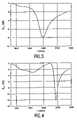
- FIG. 3is a graph of simulated return loss S 11 in dB against frequency f in MHz for the antenna of FIG. 2 , with the first pin fed and the second pin grounded;
- FIG. 4is a graph of simulated return loss S 11 in dB against frequency f in MHz for the antenna of FIG. 2 , with the first pin fed and the second pin open circuit;
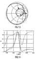
- FIG. 5is a plan view of an antenna arrangement tunable over a wide frequency range
- FIG. 6is a graph of simulated return loss S 11 in dB against frequency f in MHz for the antenna of FIG. 5 , with the value of the inductor loading the second pin varied from 0 to 64 nH;
- FIG. 7is a graph of simulated return loss S 11 in dB against frequency f in MHz for the antenna of FIG. 5 , with additional matching and with the value of the inductor loading the second pin varied from 0 to 64 nH;
- FIG. 8is a Smith chart showing simulated return loss S 11 for the antenna of FIG. 5 in GSM mode over the frequency range 800 to 3000 MHz;
- FIG. 9is a graph showing the efficiency E against frequency f in MHz for the antenna of FIG. 5 in GSM mode
- FIG. 10is a graph showing the attenuation A in dB against frequency f in MHz for the antenna of FIG. 5 in GSM mode;
- FIG. 11is a Smith chart showing simulated return loss S 11 for the antenna of FIG. 5 in PCS mode over the frequency range 800 to 3000 MHz;
- FIG. 12is a graph showing the efficiency E against frequency f in MHz for the antenna of FIG. 5 in PCS mode
- FIG. 13is a Smith chart showing simulated return loss S 11 for the antenna of FIG. 5 in DCS mode over the frequency range 800 to 3000 MHz;
- FIG. 14is a graph showing the efficiency E against frequency f in MHz for the antenna of FIG. 5 in DCS mode.
- FIG. 1A perspective view of a PIFA mounted on a handset is shown in FIG. 1 .
- the PIFAcomprises a rectangular patch conductor 102 supported parallel to a ground plane 104 forming part of the handset.
- the antennais fed via a first (feed) pin 106 , and connected to the ground plane 104 by a second (shorting) pin 108 .
- the patch conductor 102has dimensions 20 ⁇ 10 mm and is located 8 mm above the ground plane 104 which measures 40 ⁇ 100 ⁇ 1 mm.
- the feed pin 106is located at a corner of both the patch conductor 102 and ground plane 104 , and the shorting pin 108 is separated from the feed pin 106 by 3 mm.
- the impedance of a PIFAis inductive.
- the currents on the feed and shorting pins 106 , 108are the sum of balanced mode (equal and oppositely directed, non-radiating) and radiating mode (equally directed) currents.
- the feed and shorting pins 106 , 108form a short-circuit transmission line, which has an inductive reactance because of its very short length relative to a wavelength (8 mm, or 0.05 ⁇ at 2 GHz, in the embodiment shown in FIG. 1 ).
- FIG. 2is a perspective view of a variation on the standard PIFA, disclosed in our co-pending International patent application WO 02/60005 in which a slot 202 is provided in the patch conductor 102 between the feed pin 106 and shorting pin 108 .
- the presence of the slotaffects the balanced mode impedance of the antenna arrangement by increasing the length of the short circuit transmission line formed by the feed pin 106 and shorting pin 108 , which enables the inductive component of the impedance of the antenna to be significantly reduced.
- the slot 202greatly increases the length of the short-circuit transmission line formed by the feed and shorting pins 106 , 108 , thereby enabling the impedance of the transmission line to be made less inductive.
- This arrangementis therefore known as a Differentially Slotted PIFA (DS-PIFA).
- DS-PIFADifferentially Slotted PIFA
- the presence of the slotprovides an impedance transformation.
- the impedance transformationis by a factor of approximately four if the slot 202 is centrally located in the patch conductor 102 .
- An asymmetrical arrangement of the slot 202 on the patch conductor 102can be used to adjust this impedance transformation, enabling the resistive impedance of the antenna to be adjusted for better matching to any required circuit impedance, for example 50 ⁇ .
- a second operational bandcan be provided from the antenna shown in FIG. 2 by leaving the shorting pin 108 open circuit.
- the antennafunctions as a meandered Planar Inverted-L Antenna (PILA), as disclosed in our co-pending International patent application WO 02/71541 (unpublished at the priority date of the present invention).
- PILAPlanar Inverted-L Antenna
- Operation of a PILAcan best be understood by recognising that the shorting pin in a conventional PIFA performs a matching function, but this match is only effective at one frequency and is at the expense of the match at other frequencies.
- the shorting pinis omitted or left open circuit.
- dual-mode operationis enabled by connecting the second pin 108 to ground via a switch.
- the antennaWhen the switch is closed the antenna functions as a DS-PIFA, and when the switch is open the antenna functions as a meandered PILA. Simulations were performed to determine the performance of an antenna having the typical PIFA dimensions detailed above.
- the slot 202is 1 mm wide, starts centrally between the two pins 106 , 108 then runs parallel to the edge of the patch conductor 102 and 0.5 mm from its edge.
- FIGS. 3 and 4show simulated results for the return loss S 11 in DS-PIFA and PILA modes respectively.
- the present inventionaddresses the requirement for antennas which can operate over a wide bandwidth, rather than in a limited number of discrete bands.
- a plan view of an embodiment of the present inventionis shown in FIG. 5 .
- the patch conductor 102has dimensions 23 ⁇ 11 mm and is located 8 mm above the ground plane 104 .
- the slot 202has a width of 1 mm, runs parallel to and 1 mm from the top and right and bottom edges of the patch conductor 102 and ends 4.5 mm from the left edge of the patch conductor.
- a RF signal source 502is fed to the patch conductor 102 via the first pin 106 .
- the second pin 108is connected to first and second switches 504 , 506 , and a third pin 508 is provided, connected to a third switch 510 .
- the basic operation of the antennacomprises three modes, for operation in GSM (Global System for Mobile Communications), DCS and PCS (Personal Communication. Services) frequency bands.
- a fourth mode to cover UMTSUniversal Mobile Telecommunication
- GSMfirst low frequency
- the first switch 504is open, the third switch 510 is closed, connecting the third pin 508 to the ground plane 104 , and the antenna operates as a meandered PIFA.
- a capacitor 512connected between the first and third pins 106 , 508 , tunes out the balanced mode inductance of the meandered PIFA and provides a degree of broadbanding.
- a second high frequency (PCS) modearound 1900 MHz, the third switch 510 is open while the first and second switches 504 , 506 are closed, connecting the second pin 108 to the ground plane 104 , and the antenna operates as a DS-PIFA.
- DCSthird
- the second switchis opened thereby loading the second pin 108 with an inductor 514 , which has the effect of lowering the resonant frequency.
- a shunt inductor 516is provided to balance out the capacitive impedance of the antenna in DCS and PCS modes, caused by the length of the slot 202 . Its effect is countered in GSM mode by the shunt capacitor 512 , which is not in circuit in DCS and PCS modes.
- the antennacan be tuned over a wide frequency range.
- the inductor 514has a small value
- the second pin 108is close to being grounded and the antenna functions as a DS-PIFA.
- the inductor 514has a high value
- the second pin 108is close to open circuit and the antenna functions as a meandered PILA.
- FIG. 6is a graph of simulated return loss S 11 with the second and third switches 506 , 510 open circuit and the value of the inductor 514 varied from 0 to 64 nH.
- the response having the highest frequency resonancecorresponds to an inductor value of 0 nH, the next highest to an inductor value of 1 nH, with subsequent curves corresponding to successive doubling of the inductor value to a maximum of 64 nH.
- the responsesare simulated in a 200 ⁇ system (reflecting the high radiating mode impedance transformation because of the slot location, necessary for an effective meander in GSM mode).
- a variable inductor 514can be implemented in a number of ways. One way is to provide a range of inductors which can be switched individually and in combination to provide a range of values. Another way is to provide a continuously variable capacitor in parallel with the inductor, provided the frequency is below the anti-resonance frequency of the parallel combination of the capacitor and inductor (the anti-resonance frequency being tuned by the capacitor). Such a capacitor could for example be a varactor (at low power levels) or a MEMS (Micro ElectroMagnetic Systems) device. For switching in the variable inductor, as well as the first, second and third switches 504 , 506 , 510 , MEMS switches are particularly appropriate because of their low on resistance and high off resistance.
- the antennacan be tuned over a bandwidth of nearly an octave.
- the resistance at resonance of the meandered PILA modeis much lower than that of the DS-PIFA mode, because the location of the slot 202 provides no impedance transformation in the meandered PILA mode.
- the matchdeteriorates as the resonant frequency is reduced.
- tuning over a range of approximately 200–300 MHzis possible without significant degradation of the match. This is sufficient to cover UMTS, PCS and DCS frequency bands.
- the matchcan be significantly improved by use of a matching circuit which provides a larger upward impedance transformation at low frequencies is than at high frequencies.
- a simple example of thisis a series capacitor connected to the antenna followed by a shunt inductor. Using a capacitance of 2 pF and an inductance of 25 nH, the simulated results are modified to those shown in FIG. 7 . Here the match is much better maintained over the full tunable frequency range.
- a higher impedancecould also be achieved by closing the third switch 510 : this will have little effect on the frequency responses but the antenna will then function as a meandered PIFA rather than a meandered PILA for high values of the inductor 514 .
- FIG. 8is a Smith chart showing its simulated return loss.
- the marker s 1corresponds to a frequency of 880 MHz and the marker s 2 to a frequency of 960 MHz.
- the switchesare simulated as MEMS switches with a series resistance of 0.5 ⁇ in the on state and a series reactance of 0.02 pF in the off state.
- the return loss S 11is not especially good, at approximately ⁇ 5 dB in band, it is sufficient to pass through the switches without significant loss, when the transmit and receive bands can be individually matched to an acceptable level.
- the efficiency E of the antenna in GSM modeis shown in FIG. 9 , where the mismatch loss is shown as a dashed line, the circuit loss as a chain-dashed line, and the combined loss as a solid line.
- FIG. 10shows the attenuation A (in dB) of the antenna, demonstrating that it provides over 30 dB rejection of the second harmonic, and about 20 dB rejection of the third harmonic.
- This attenuationcould be further improved by the addition of a conductor linking the first and third pins 106 , 508 , as disclosed in our co-pending unpublished International patent application IB 02/02575 (Applicant's reference PHGB 010120).
- FIG. 11is a Smith chart showing its simulated return loss.
- the marker s 1corresponds to a frequency of 1850 MHz and the marker s 2 to a frequency of 1990 MHz.
- the matchis very good, although at a high impedance of 200 ⁇ . This is because of the large radiating mode impedance transformation provided by the location of the slot 202 , which is required for an effective meander in GSM mode.
- a high impedancecan be advantageous for switching, and it can be reduced if the height of the antenna is reduced.
- the efficiency E of the antenna in PCS modeis shown in FIG. 12 , where the mismatch loss is shown as a dashed line, the circuit loss as a chain-dashed line, and the combined loss as a solid line. The circuit losses are approximately 10%.
- FIG. 13is a Smith chart showing its simulated return loss.
- the marker s 1corresponds to a frequency of 1710 MHz and the marker s 2 to a frequency of 1880 MHz.
- inductive loading of the second pin 108 by the inductor 514is used.
- the match and bandwidthare similar to those for the PCS mode.
- the efficiency Eshown in FIG. 14 (with the same meanings for line types as previously), is also similar to that in PCS mode, despite the inductive loading in the shorting pin.
- the provision of the third pin 508 and the associated mode of operation when the third switch is closedis not an essential feature of the present invention, which merely requires a first connection to the patch conductor 102 for signals and a second connection between the patch conductor 102 and ground plane 104 having a variable impedance which can take a range of values between open and short circuit.
- a wide range of alternative embodiments having additional connection points and/or additional slotsis possible.
- the present inventionmay be implemented without the need for any switches.
- the third pin 508can also be inductively loaded, thereby enabling coverage of cellular transmissions around 824 to 894 MHz. Provision of a further switch and inductor connected to the third pin 508 , in a similar arrangement to the first switch 504 and associated inductor 514 connected to the second pin 108 , would enable coverage of this band and the GSM band.
Landscapes
- Engineering & Computer Science (AREA)
- Computer Networks & Wireless Communication (AREA)
- Waveguide Aerials (AREA)
- Variable-Direction Aerials And Aerial Arrays (AREA)
- Details Of Aerials (AREA)
Abstract
Description
Claims (10)
Applications Claiming Priority (3)
| Application Number | Priority Date | Filing Date | Title |
|---|---|---|---|
| GBGB0209818.4AGB0209818D0 (en) | 2002-04-30 | 2002-04-30 | Antenna arrangement |
| GB0209818.4 | 2002-04-30 | ||
| PCT/IB2003/001538WO2003094290A1 (en) | 2002-04-30 | 2003-04-17 | Antenna arrangement |
Publications (2)
| Publication Number | Publication Date |
|---|---|
| US20060055606A1 US20060055606A1 (en) | 2006-03-16 |
| US7215283B2true US7215283B2 (en) | 2007-05-08 |
Family
ID=9935750
Family Applications (1)
| Application Number | Title | Priority Date | Filing Date |
|---|---|---|---|
| US10/512,617Expired - LifetimeUS7215283B2 (en) | 2002-04-30 | 2003-04-17 | Antenna arrangement |
Country Status (10)
| Country | Link |
|---|---|
| US (1) | US7215283B2 (en) |
| EP (1) | EP1502322B1 (en) |
| JP (1) | JP4191677B2 (en) |
| KR (1) | KR100993439B1 (en) |
| CN (1) | CN1650469A (en) |
| AT (1) | ATE332017T1 (en) |
| AU (1) | AU2003226592A1 (en) |
| DE (1) | DE60306513T2 (en) |
| GB (1) | GB0209818D0 (en) |
| WO (1) | WO2003094290A1 (en) |
Cited By (47)
| Publication number | Priority date | Publication date | Assignee | Title |
|---|---|---|---|---|
| US20070273606A1 (en)* | 2006-05-26 | 2007-11-29 | Hong Kong Applied Science and Technology Research Institude Co., Ltd. | Multi mode antenna system |
| US20080129637A1 (en)* | 2006-11-30 | 2008-06-05 | Yun-Wen Chi | Dual-band loop antenna |
| US20080291100A1 (en)* | 2006-11-30 | 2008-11-27 | Yun-Wen Chi | Dual-band loop antenna |
| US20090213015A1 (en)* | 2005-05-31 | 2009-08-27 | Nxp B.V. | Planar antenna assembly with impedance matching and reduced user interaction, for a rf communication equipment |
| US20100214179A1 (en)* | 2009-02-23 | 2010-08-26 | Kin-Lu Wong | Multiband antenna and communication device having the same |
| US20110148723A1 (en)* | 2008-06-23 | 2011-06-23 | Erik Bengtsson | Tunable Antenna Arrangement |
| US20110183633A1 (en)* | 2009-08-27 | 2011-07-28 | Isao Ohba | Antenna Apparatus and Communication Apparatus |
| WO2012121865A1 (en)* | 2011-03-07 | 2012-09-13 | Apple Inc. | Tunable antenna system with receiver diversity |
| US20120299785A1 (en)* | 2011-05-27 | 2012-11-29 | Peter Bevelacqua | Dynamically adjustable antenna supporting multiple antenna modes |
| US8798554B2 (en) | 2012-02-08 | 2014-08-05 | Apple Inc. | Tunable antenna system with multiple feeds |
| US8866689B2 (en) | 2011-07-07 | 2014-10-21 | Pulse Finland Oy | Multi-band antenna and methods for long term evolution wireless system |
| US20140347227A1 (en)* | 2013-05-24 | 2014-11-27 | Microsoft Corporation | Side face antenna for a computing device case |
| US8988296B2 (en) | 2012-04-04 | 2015-03-24 | Pulse Finland Oy | Compact polarized antenna and methods |
| US9070969B2 (en) | 2010-07-06 | 2015-06-30 | Apple Inc. | Tunable antenna systems |
| US9123990B2 (en) | 2011-10-07 | 2015-09-01 | Pulse Finland Oy | Multi-feed antenna apparatus and methods |
| US9190712B2 (en) | 2012-02-03 | 2015-11-17 | Apple Inc. | Tunable antenna system |
| US9203154B2 (en) | 2011-01-25 | 2015-12-01 | Pulse Finland Oy | Multi-resonance antenna, antenna module, radio device and methods |
| US9246221B2 (en) | 2011-03-07 | 2016-01-26 | Apple Inc. | Tunable loop antennas |
| US9246210B2 (en) | 2010-02-18 | 2016-01-26 | Pulse Finland Oy | Antenna with cover radiator and methods |
| US9350081B2 (en) | 2014-01-14 | 2016-05-24 | Pulse Finland Oy | Switchable multi-radiator high band antenna apparatus |
| US9350069B2 (en) | 2012-01-04 | 2016-05-24 | Apple Inc. | Antenna with switchable inductor low-band tuning |
| US9444130B2 (en) | 2013-04-10 | 2016-09-13 | Apple Inc. | Antenna system with return path tuning and loop element |
| US9461371B2 (en) | 2009-11-27 | 2016-10-04 | Pulse Finland Oy | MIMO antenna and methods |
| US9484619B2 (en) | 2011-12-21 | 2016-11-01 | Pulse Finland Oy | Switchable diversity antenna apparatus and methods |
| US9531058B2 (en) | 2011-12-20 | 2016-12-27 | Pulse Finland Oy | Loosely-coupled radio antenna apparatus and methods |
| US9543639B2 (en) | 2013-05-24 | 2017-01-10 | Microsoft Technology Licensing, Llc | Back face antenna in a computing device case |
| US9559433B2 (en) | 2013-03-18 | 2017-01-31 | Apple Inc. | Antenna system having two antennas and three ports |
| US9590308B2 (en) | 2013-12-03 | 2017-03-07 | Pulse Electronics, Inc. | Reduced surface area antenna apparatus and mobile communications devices incorporating the same |
| US9634383B2 (en) | 2013-06-26 | 2017-04-25 | Pulse Finland Oy | Galvanically separated non-interacting antenna sector apparatus and methods |
| US9647338B2 (en) | 2013-03-11 | 2017-05-09 | Pulse Finland Oy | Coupled antenna structure and methods |
| US9673507B2 (en) | 2011-02-11 | 2017-06-06 | Pulse Finland Oy | Chassis-excited antenna apparatus and methods |
| US9680212B2 (en) | 2013-11-20 | 2017-06-13 | Pulse Finland Oy | Capacitive grounding methods and apparatus for mobile devices |
| US9698466B2 (en) | 2013-05-24 | 2017-07-04 | Microsoft Technology Licensing, Llc | Radiating structure formed as a part of a metal computing device case |
| US9722308B2 (en) | 2014-08-28 | 2017-08-01 | Pulse Finland Oy | Low passive intermodulation distributed antenna system for multiple-input multiple-output systems and methods of use |
| US9761951B2 (en) | 2009-11-03 | 2017-09-12 | Pulse Finland Oy | Adjustable antenna apparatus and methods |
| US9906260B2 (en) | 2015-07-30 | 2018-02-27 | Pulse Finland Oy | Sensor-based closed loop antenna swapping apparatus and methods |
| US9917346B2 (en) | 2011-02-11 | 2018-03-13 | Pulse Finland Oy | Chassis-excited antenna apparatus and methods |
| US9948002B2 (en) | 2014-08-26 | 2018-04-17 | Pulse Finland Oy | Antenna apparatus with an integrated proximity sensor and methods |
| US9973228B2 (en) | 2014-08-26 | 2018-05-15 | Pulse Finland Oy | Antenna apparatus with an integrated proximity sensor and methods |
| US9979078B2 (en) | 2012-10-25 | 2018-05-22 | Pulse Finland Oy | Modular cell antenna apparatus and methods |
| US10069209B2 (en) | 2012-11-06 | 2018-09-04 | Pulse Finland Oy | Capacitively coupled antenna apparatus and methods |
| US10079428B2 (en) | 2013-03-11 | 2018-09-18 | Pulse Finland Oy | Coupled antenna structure and methods |
| US10128573B2 (en) | 2014-10-17 | 2018-11-13 | Wispry, Inc. | Tunable multiple-resonance antenna systems, devices, and methods for handsets operating in low LTE bands with wide duplex spacing |
| US10355339B2 (en) | 2013-03-18 | 2019-07-16 | Apple Inc. | Tunable antenna with slot-based parasitic element |
| US10418717B2 (en) | 2015-05-18 | 2019-09-17 | Cavendish Kinetics, Inc. | Method and apparatus of maintaining constant antenna resonant frequency and impedance match in the presence of environmental changes and head/hand effect using variable reactance antenna aperture tuners |
| WO2023067196A1 (en) | 2021-10-22 | 2023-04-27 | Ignion, S.L. | SELF-TUNABLE IoT DEVICE AND RADIATING SYSTEM BASED ON NON-RESONANT RADIATION ELEMENTS |
| WO2024218370A1 (en) | 2023-04-21 | 2024-10-24 | Ignion, S.L. | SELF-TUNABLE IoT DEVICE AND RADIATING SYSTEM BASED ON NON-RESONANT RADIATION ELEMENTS WITH ENHANCED MATCHING TOPOLOGIES |
Families Citing this family (81)
| Publication number | Priority date | Publication date | Assignee | Title |
|---|---|---|---|---|
| TW200511649A (en)* | 2003-07-21 | 2005-03-16 | Ipr Licensing Inc | Multi-band antenna for wireless applications |
| FI120607B (en) | 2003-10-31 | 2009-12-15 | Pulse Finland Oy | The multi-band planar antenna |
| JP2005260592A (en)* | 2004-03-11 | 2005-09-22 | Fujitsu Ltd | Antenna device, directivity control method, and communication device |
| JP3852113B2 (en)* | 2004-03-31 | 2006-11-29 | 東陶機器株式会社 | Microstrip antenna and high frequency sensor |
| JP2005303721A (en)* | 2004-04-13 | 2005-10-27 | Sharp Corp | Antenna and portable radio using the same |
| WO2006019910A1 (en)* | 2004-07-26 | 2006-02-23 | Kyocera Wireless Corp. | Full-duplex antenna system and method |
| JP3889423B2 (en) | 2004-12-16 | 2007-03-07 | 松下電器産業株式会社 | Polarization switching antenna device |
| EP1878088B1 (en) | 2005-04-27 | 2018-06-06 | Qualcomm Technologies, Inc. | Radio device having antenna arrangement suited for operating over a plurality of bands. |
| KR100713525B1 (en)* | 2005-05-04 | 2007-04-30 | 삼성전자주식회사 | Antenna device which can change operating frequency band |
| US7242364B2 (en)* | 2005-09-29 | 2007-07-10 | Nokia Corporation | Dual-resonant antenna |
| US8472908B2 (en) | 2006-04-03 | 2013-06-25 | Fractus, S.A. | Wireless portable device including internal broadcast receiver |
| US7773041B2 (en) | 2006-07-12 | 2010-08-10 | Apple Inc. | Antenna system |
| WO2008010149A1 (en)* | 2006-07-17 | 2008-01-24 | Nxp B.V. | Antenna with reduced sensitivity to user finger position |
| JP4720720B2 (en)* | 2006-11-07 | 2011-07-13 | 株式会社村田製作所 | Antenna structure and wireless communication apparatus including the same |
| US7477196B2 (en)* | 2006-12-20 | 2009-01-13 | Motorola, Inc. | Switched capacitive patch for radio frequency antennas |
| US8350761B2 (en) | 2007-01-04 | 2013-01-08 | Apple Inc. | Antennas for handheld electronic devices |
| US7595759B2 (en)* | 2007-01-04 | 2009-09-29 | Apple Inc. | Handheld electronic devices with isolated antennas |
| US7889139B2 (en) | 2007-06-21 | 2011-02-15 | Apple Inc. | Handheld electronic device with cable grounding |
| US8018389B2 (en) | 2007-01-05 | 2011-09-13 | Apple Inc. | Methods and apparatus for improving the performance of an electronic device having one or more antennas |
| US7672142B2 (en)* | 2007-01-05 | 2010-03-02 | Apple Inc. | Grounded flexible circuits |
| JP4752771B2 (en)* | 2007-01-19 | 2011-08-17 | 株式会社村田製作所 | Method for suppressing unwanted wave radiation of antenna structure, antenna structure, and radio communication apparatus including the same |
| EP2140517A1 (en) | 2007-03-30 | 2010-01-06 | Fractus, S.A. | Wireless device including a multiband antenna system |
| US7911387B2 (en)* | 2007-06-21 | 2011-03-22 | Apple Inc. | Handheld electronic device antennas |
| US9838059B2 (en) | 2007-06-21 | 2017-12-05 | Apple Inc. | Handheld electronic touch screen communication device |
| US7612725B2 (en)* | 2007-06-21 | 2009-11-03 | Apple Inc. | Antennas for handheld electronic devices with conductive bezels |
| US7876274B2 (en)* | 2007-06-21 | 2011-01-25 | Apple Inc. | Wireless handheld electronic device |
| KR100891623B1 (en)* | 2007-08-13 | 2009-04-02 | 주식회사 이엠따블유안테나 | Resonant Frequency Variable Antenna |
| US7768462B2 (en)* | 2007-08-22 | 2010-08-03 | Apple Inc. | Multiband antenna for handheld electronic devices |
| US7864123B2 (en)* | 2007-08-28 | 2011-01-04 | Apple Inc. | Hybrid slot antennas for handheld electronic devices |
| US20090061966A1 (en)* | 2007-09-05 | 2009-03-05 | Motorola, Inc. | Antenna and speaker assembly |
| US7551142B1 (en)* | 2007-12-13 | 2009-06-23 | Apple Inc. | Hybrid antennas with directly fed antenna slots for handheld electronic devices |
| US8441404B2 (en)* | 2007-12-18 | 2013-05-14 | Apple Inc. | Feed networks for slot antennas in electronic devices |
| US8373610B2 (en)* | 2007-12-18 | 2013-02-12 | Apple Inc. | Microslot antennas for electronic devices |
| US8599088B2 (en)* | 2007-12-18 | 2013-12-03 | Apple Inc. | Dual-band antenna with angled slot for portable electronic devices |
| US20090153412A1 (en)* | 2007-12-18 | 2009-06-18 | Bing Chiang | Antenna slot windows for electronic device |
| US7705795B2 (en) | 2007-12-18 | 2010-04-27 | Apple Inc. | Antennas with periodic shunt inductors |
| EP2081253A1 (en)* | 2008-01-18 | 2009-07-22 | Laird Technologies AB | Antenna device and portable radio communication device comprising such an antenna device |
| US7933123B2 (en) | 2008-04-11 | 2011-04-26 | Apple Inc. | Portable electronic device with two-piece housing |
| US8106836B2 (en)* | 2008-04-11 | 2012-01-31 | Apple Inc. | Hybrid antennas for electronic devices |
| US8102319B2 (en) | 2008-04-11 | 2012-01-24 | Apple Inc. | Hybrid antennas for electronic devices |
| KR101480555B1 (en)* | 2008-06-19 | 2015-01-09 | 삼성전자주식회사 | Antenna device for portable terminal |
| CN101320840B (en)* | 2008-06-24 | 2012-02-22 | 东南大学 | Multi-stopband ultra-wideband antenna based on miniaturized dual-mode resonators and zero-order resonators |
| CN102106038A (en)* | 2008-07-24 | 2011-06-22 | Nxp股份有限公司 | Antenna device and radio equipment including antenna device |
| US8648770B2 (en) | 2008-09-05 | 2014-02-11 | Antennas Direct, Inc. | Smart antenna systems suitable for reception of digital television signals |
| JP2010062976A (en)* | 2008-09-05 | 2010-03-18 | Sony Ericsson Mobile Communications Ab | Notch antenna and wireless device |
| US8174452B2 (en)* | 2008-09-25 | 2012-05-08 | Apple Inc. | Cavity antenna for wireless electronic devices |
| EP2178167A1 (en)* | 2008-10-17 | 2010-04-21 | Epcos AG | Antenna and method for operating an antenna |
| US8665164B2 (en)* | 2008-11-19 | 2014-03-04 | Apple Inc. | Multiband handheld electronic device slot antenna |
| KR100924769B1 (en) | 2009-02-23 | 2009-11-05 | 주식회사 네오펄스 | Band select antenna |
| US8228242B2 (en) | 2009-09-25 | 2012-07-24 | Sony Ericsson Mobile Communications Ab | Ultra wide band secondary antennas and wireless devices using the same |
| US8270914B2 (en)* | 2009-12-03 | 2012-09-18 | Apple Inc. | Bezel gap antennas |
| US9172139B2 (en)* | 2009-12-03 | 2015-10-27 | Apple Inc. | Bezel gap antennas |
| US8847833B2 (en) | 2009-12-29 | 2014-09-30 | Pulse Finland Oy | Loop resonator apparatus and methods for enhanced field control |
| DE112010005394T5 (en)* | 2010-03-15 | 2012-12-27 | Laird Technologies Ab | Multi-band frame antenna and portable radio communication device having such an antenna |
| US9160056B2 (en) | 2010-04-01 | 2015-10-13 | Apple Inc. | Multiband antennas formed from bezel bands with gaps |
| US9406998B2 (en) | 2010-04-21 | 2016-08-02 | Pulse Finland Oy | Distributed multiband antenna and methods |
| KR101687632B1 (en) | 2010-05-10 | 2016-12-20 | 삼성전자주식회사 | Re-configurable built-in antenna for portable terminal |
| US8482467B2 (en) | 2010-06-25 | 2013-07-09 | Apple Inc. | Customizable antenna structures for adjusting antenna performance in electronic devices |
| KR101349222B1 (en)* | 2010-07-23 | 2014-01-08 | 한국전자통신연구원 | An antenna using composite right/left-handed structure |
| US8489162B1 (en)* | 2010-08-17 | 2013-07-16 | Amazon Technologies, Inc. | Slot antenna within existing device component |
| JP5860211B2 (en)* | 2010-12-13 | 2016-02-16 | 富士通株式会社 | antenna |
| US8947303B2 (en) | 2010-12-20 | 2015-02-03 | Apple Inc. | Peripheral electronic device housing members with gaps and dielectric coatings |
| US9450291B2 (en) | 2011-07-25 | 2016-09-20 | Pulse Finland Oy | Multiband slot loop antenna apparatus and methods |
| KR101357724B1 (en)* | 2011-12-29 | 2014-02-03 | 주식회사 바켄 | Apparatus for multiband antenna |
| US9002297B2 (en) | 2012-11-06 | 2015-04-07 | Htc Corporation | Mobile device and tunable antenna therein |
| CN103972656A (en) | 2013-02-04 | 2014-08-06 | 华为终端有限公司 | Antenna device and terminal equipment |
| CN104425892A (en)* | 2013-08-22 | 2015-03-18 | 深圳富泰宏精密工业有限公司 | Adjustable antenna device and wireless communication apparatus with same |
| KR101465371B1 (en)* | 2013-12-27 | 2014-11-26 | 현대다이모스(주) | Transmission line switching method and device |
| CN106159450A (en)* | 2015-03-26 | 2016-11-23 | 联想(北京)有限公司 | Loop aerial and electronic equipment |
| CN104852148A (en)* | 2015-04-03 | 2015-08-19 | 青岛海信移动通信技术股份有限公司 | Tunable antenna and terminal |
| KR20170115716A (en) | 2016-04-08 | 2017-10-18 | 현대자동차주식회사 | Antenna apparatus, method for controlling thereof vehicle having the same |
| US10230153B2 (en)* | 2016-06-20 | 2019-03-12 | Shure Acquisition Holdings, Inc. | Secondary antenna for wireless microphone |
| CN108650818B (en)* | 2016-08-16 | 2020-08-18 | Oppo广东移动通信有限公司 | Method for processing casing, casing and mobile terminal |
| US10522915B2 (en) | 2017-02-01 | 2019-12-31 | Shure Acquisition Holdings, Inc. | Multi-band slotted planar antenna |
| WO2018156829A1 (en)* | 2017-02-24 | 2018-08-30 | AMI Research & Development, LLC | Slot line volumetric antenna |
| EP3977558A1 (en)* | 2019-05-29 | 2022-04-06 | Robert Bosch GmbH | An antenna system |
| CN110718747A (en)* | 2019-09-16 | 2020-01-21 | 努比亚技术有限公司 | Terminal shell and terminal |
| TWI715313B (en)* | 2019-11-27 | 2021-01-01 | 和碩聯合科技股份有限公司 | Antenna structure and communication device |
| CN113131181B (en)* | 2019-12-30 | 2023-11-21 | 成都鼎桥通信技术有限公司 | Terminal Equipment |
| KR20220080544A (en) | 2020-12-07 | 2022-06-14 | 삼성전자주식회사 | Electronic device comprising antenna and method for manufacturing thereof |
| CN113422619B (en)* | 2021-06-18 | 2022-05-27 | 安徽安努奇科技有限公司 | Tuning circuit and communication equipment |
Citations (7)
| Publication number | Priority date | Publication date | Assignee | Title |
|---|---|---|---|---|
| US5943016A (en)* | 1995-12-07 | 1999-08-24 | Atlantic Aerospace Electronics, Corp. | Tunable microstrip patch antenna and feed network therefor |
| EP0993070A1 (en) | 1998-09-30 | 2000-04-12 | Nec Corporation | Inverted-F antenna with switched impedance |
| EP0997974A1 (en) | 1998-10-30 | 2000-05-03 | Lk-Products Oy | Planar antenna with two resonating frequencies |
| WO2000071535A1 (en) | 1999-05-21 | 2000-11-30 | Scios Inc. | INDOLE-TYPE DERIVATIVES AS INHIBITORS OF p38 KINASE |
| US6229487B1 (en) | 2000-02-24 | 2001-05-08 | Ericsson Inc. | Inverted-F antennas having non-linear conductive elements and wireless communicators incorporating the same |
| JP2001274619A (en) | 2000-03-27 | 2001-10-05 | Nippon Soken Inc | Inverted-f antenna |
| WO2002060005A1 (en) | 2001-01-23 | 2002-08-01 | Koninklijke Philips Electronics N.V. | Pifa antenna arrangement |
Family Cites Families (2)
| Publication number | Priority date | Publication date | Assignee | Title |
|---|---|---|---|---|
| JPH1028013A (en)* | 1996-07-11 | 1998-01-27 | Matsushita Electric Ind Co Ltd | Planar antenna |
| JPH10224142A (en)* | 1997-02-04 | 1998-08-21 | Kenwood Corp | Resonance frequency switchable inverse f-type antenna |
- 2002
- 2002-04-30GBGBGB0209818.4Apatent/GB0209818D0/ennot_activeCeased
- 2003
- 2003-04-17KRKR1020047017348Apatent/KR100993439B1/ennot_activeExpired - Lifetime
- 2003-04-17WOPCT/IB2003/001538patent/WO2003094290A1/enactiveIP Right Grant
- 2003-04-17JPJP2004502410Apatent/JP4191677B2/ennot_activeExpired - Fee Related
- 2003-04-17EPEP03747512Apatent/EP1502322B1/ennot_activeExpired - Lifetime
- 2003-04-17DEDE60306513Tpatent/DE60306513T2/ennot_activeExpired - Lifetime
- 2003-04-17CNCNA038097206Apatent/CN1650469A/enactivePending
- 2003-04-17ATAT03747512Tpatent/ATE332017T1/ennot_activeIP Right Cessation
- 2003-04-17USUS10/512,617patent/US7215283B2/ennot_activeExpired - Lifetime
- 2003-04-17AUAU2003226592Apatent/AU2003226592A1/ennot_activeAbandoned
Patent Citations (9)
| Publication number | Priority date | Publication date | Assignee | Title |
|---|---|---|---|---|
| US5943016A (en)* | 1995-12-07 | 1999-08-24 | Atlantic Aerospace Electronics, Corp. | Tunable microstrip patch antenna and feed network therefor |
| EP0993070A1 (en) | 1998-09-30 | 2000-04-12 | Nec Corporation | Inverted-F antenna with switched impedance |
| EP0993070B1 (en) | 1998-09-30 | 2005-03-30 | Nec Corporation | Inverted-F antenna with switched impedance |
| EP0997974A1 (en) | 1998-10-30 | 2000-05-03 | Lk-Products Oy | Planar antenna with two resonating frequencies |
| EP0997974B1 (en) | 1998-10-30 | 2002-01-09 | Filtronic LK Oy | Planar antenna with two resonating frequencies |
| WO2000071535A1 (en) | 1999-05-21 | 2000-11-30 | Scios Inc. | INDOLE-TYPE DERIVATIVES AS INHIBITORS OF p38 KINASE |
| US6229487B1 (en) | 2000-02-24 | 2001-05-08 | Ericsson Inc. | Inverted-F antennas having non-linear conductive elements and wireless communicators incorporating the same |
| JP2001274619A (en) | 2000-03-27 | 2001-10-05 | Nippon Soken Inc | Inverted-f antenna |
| WO2002060005A1 (en) | 2001-01-23 | 2002-08-01 | Koninklijke Philips Electronics N.V. | Pifa antenna arrangement |
Cited By (64)
| Publication number | Priority date | Publication date | Assignee | Title |
|---|---|---|---|---|
| US7884769B2 (en)* | 2005-05-31 | 2011-02-08 | Epcos Ag | Planar antenna assembly with impedance matching and reduced user interaction for a RF communication equipment |
| US20090213015A1 (en)* | 2005-05-31 | 2009-08-27 | Nxp B.V. | Planar antenna assembly with impedance matching and reduced user interaction, for a rf communication equipment |
| US7616158B2 (en)* | 2006-05-26 | 2009-11-10 | Hong Kong Applied Science And Technology Research Institute Co., Ltd. | Multi mode antenna system |
| US20070273606A1 (en)* | 2006-05-26 | 2007-11-29 | Hong Kong Applied Science and Technology Research Institude Co., Ltd. | Multi mode antenna system |
| US20080129637A1 (en)* | 2006-11-30 | 2008-06-05 | Yun-Wen Chi | Dual-band loop antenna |
| US20080291100A1 (en)* | 2006-11-30 | 2008-11-27 | Yun-Wen Chi | Dual-band loop antenna |
| US7639194B2 (en)* | 2006-11-30 | 2009-12-29 | Auden Techno Corp. | Dual-band loop antenna |
| US20110148723A1 (en)* | 2008-06-23 | 2011-06-23 | Erik Bengtsson | Tunable Antenna Arrangement |
| US8674889B2 (en)* | 2008-06-23 | 2014-03-18 | Nokia Corporation | Tunable antenna arrangement |
| US7978140B2 (en)* | 2009-02-23 | 2011-07-12 | Acer Inc. | Multiband antenna and communication device having the same |
| US20100214179A1 (en)* | 2009-02-23 | 2010-08-26 | Kin-Lu Wong | Multiband antenna and communication device having the same |
| US8942641B2 (en)* | 2009-08-27 | 2015-01-27 | Kabushiki Kaisha Toshiba | Antenna apparatus and communication apparatus |
| US20110183633A1 (en)* | 2009-08-27 | 2011-07-28 | Isao Ohba | Antenna Apparatus and Communication Apparatus |
| US8699964B2 (en)* | 2009-08-27 | 2014-04-15 | Kabushiki Kaisha Toshiba | Antenna apparatus and communication apparatus |
| US20140220906A1 (en)* | 2009-08-27 | 2014-08-07 | Kabushiki Kaisha Toshiba | Antenna apparatus and communication apparatus |
| US9761951B2 (en) | 2009-11-03 | 2017-09-12 | Pulse Finland Oy | Adjustable antenna apparatus and methods |
| US9461371B2 (en) | 2009-11-27 | 2016-10-04 | Pulse Finland Oy | MIMO antenna and methods |
| US9246210B2 (en) | 2010-02-18 | 2016-01-26 | Pulse Finland Oy | Antenna with cover radiator and methods |
| US9893755B2 (en) | 2010-07-06 | 2018-02-13 | Apple Inc. | Tunable antenna systems |
| US9070969B2 (en) | 2010-07-06 | 2015-06-30 | Apple Inc. | Tunable antenna systems |
| US10171125B2 (en) | 2010-07-06 | 2019-01-01 | Apple Inc. | Tunable antenna systems |
| US9203154B2 (en) | 2011-01-25 | 2015-12-01 | Pulse Finland Oy | Multi-resonance antenna, antenna module, radio device and methods |
| US9673507B2 (en) | 2011-02-11 | 2017-06-06 | Pulse Finland Oy | Chassis-excited antenna apparatus and methods |
| US9917346B2 (en) | 2011-02-11 | 2018-03-13 | Pulse Finland Oy | Chassis-excited antenna apparatus and methods |
| WO2012121865A1 (en)* | 2011-03-07 | 2012-09-13 | Apple Inc. | Tunable antenna system with receiver diversity |
| US9166279B2 (en) | 2011-03-07 | 2015-10-20 | Apple Inc. | Tunable antenna system with receiver diversity |
| US9246221B2 (en) | 2011-03-07 | 2016-01-26 | Apple Inc. | Tunable loop antennas |
| CN102684722A (en)* | 2011-03-07 | 2012-09-19 | 苹果公司 | Tunable antenna system with receiver diversity |
| CN102684722B (en)* | 2011-03-07 | 2015-04-22 | 苹果公司 | Tunable antenna system with receiver diversity |
| US9024823B2 (en)* | 2011-05-27 | 2015-05-05 | Apple Inc. | Dynamically adjustable antenna supporting multiple antenna modes |
| US20120299785A1 (en)* | 2011-05-27 | 2012-11-29 | Peter Bevelacqua | Dynamically adjustable antenna supporting multiple antenna modes |
| US8866689B2 (en) | 2011-07-07 | 2014-10-21 | Pulse Finland Oy | Multi-band antenna and methods for long term evolution wireless system |
| US9123990B2 (en) | 2011-10-07 | 2015-09-01 | Pulse Finland Oy | Multi-feed antenna apparatus and methods |
| US9531058B2 (en) | 2011-12-20 | 2016-12-27 | Pulse Finland Oy | Loosely-coupled radio antenna apparatus and methods |
| US9484619B2 (en) | 2011-12-21 | 2016-11-01 | Pulse Finland Oy | Switchable diversity antenna apparatus and methods |
| US9350069B2 (en) | 2012-01-04 | 2016-05-24 | Apple Inc. | Antenna with switchable inductor low-band tuning |
| US9190712B2 (en) | 2012-02-03 | 2015-11-17 | Apple Inc. | Tunable antenna system |
| US8798554B2 (en) | 2012-02-08 | 2014-08-05 | Apple Inc. | Tunable antenna system with multiple feeds |
| US9509054B2 (en) | 2012-04-04 | 2016-11-29 | Pulse Finland Oy | Compact polarized antenna and methods |
| US8988296B2 (en) | 2012-04-04 | 2015-03-24 | Pulse Finland Oy | Compact polarized antenna and methods |
| US9979078B2 (en) | 2012-10-25 | 2018-05-22 | Pulse Finland Oy | Modular cell antenna apparatus and methods |
| US10069209B2 (en) | 2012-11-06 | 2018-09-04 | Pulse Finland Oy | Capacitively coupled antenna apparatus and methods |
| US10079428B2 (en) | 2013-03-11 | 2018-09-18 | Pulse Finland Oy | Coupled antenna structure and methods |
| US9647338B2 (en) | 2013-03-11 | 2017-05-09 | Pulse Finland Oy | Coupled antenna structure and methods |
| US10355339B2 (en) | 2013-03-18 | 2019-07-16 | Apple Inc. | Tunable antenna with slot-based parasitic element |
| US9559433B2 (en) | 2013-03-18 | 2017-01-31 | Apple Inc. | Antenna system having two antennas and three ports |
| US9444130B2 (en) | 2013-04-10 | 2016-09-13 | Apple Inc. | Antenna system with return path tuning and loop element |
| US20140347227A1 (en)* | 2013-05-24 | 2014-11-27 | Microsoft Corporation | Side face antenna for a computing device case |
| US9698466B2 (en) | 2013-05-24 | 2017-07-04 | Microsoft Technology Licensing, Llc | Radiating structure formed as a part of a metal computing device case |
| US9531059B2 (en)* | 2013-05-24 | 2016-12-27 | Microsoft Technology Licensing, Llc | Side face antenna for a computing device case |
| US9543639B2 (en) | 2013-05-24 | 2017-01-10 | Microsoft Technology Licensing, Llc | Back face antenna in a computing device case |
| US9634383B2 (en) | 2013-06-26 | 2017-04-25 | Pulse Finland Oy | Galvanically separated non-interacting antenna sector apparatus and methods |
| US9680212B2 (en) | 2013-11-20 | 2017-06-13 | Pulse Finland Oy | Capacitive grounding methods and apparatus for mobile devices |
| US9590308B2 (en) | 2013-12-03 | 2017-03-07 | Pulse Electronics, Inc. | Reduced surface area antenna apparatus and mobile communications devices incorporating the same |
| US9350081B2 (en) | 2014-01-14 | 2016-05-24 | Pulse Finland Oy | Switchable multi-radiator high band antenna apparatus |
| US9973228B2 (en) | 2014-08-26 | 2018-05-15 | Pulse Finland Oy | Antenna apparatus with an integrated proximity sensor and methods |
| US9948002B2 (en) | 2014-08-26 | 2018-04-17 | Pulse Finland Oy | Antenna apparatus with an integrated proximity sensor and methods |
| US9722308B2 (en) | 2014-08-28 | 2017-08-01 | Pulse Finland Oy | Low passive intermodulation distributed antenna system for multiple-input multiple-output systems and methods of use |
| US10128573B2 (en) | 2014-10-17 | 2018-11-13 | Wispry, Inc. | Tunable multiple-resonance antenna systems, devices, and methods for handsets operating in low LTE bands with wide duplex spacing |
| US10541475B2 (en) | 2014-10-17 | 2020-01-21 | Wispry, Inc. | Tunable multiple-resonance antenna systems, devices, and methods for handsets operating in low LTE bands with wide duplex spacing |
| US10418717B2 (en) | 2015-05-18 | 2019-09-17 | Cavendish Kinetics, Inc. | Method and apparatus of maintaining constant antenna resonant frequency and impedance match in the presence of environmental changes and head/hand effect using variable reactance antenna aperture tuners |
| US9906260B2 (en) | 2015-07-30 | 2018-02-27 | Pulse Finland Oy | Sensor-based closed loop antenna swapping apparatus and methods |
| WO2023067196A1 (en) | 2021-10-22 | 2023-04-27 | Ignion, S.L. | SELF-TUNABLE IoT DEVICE AND RADIATING SYSTEM BASED ON NON-RESONANT RADIATION ELEMENTS |
| WO2024218370A1 (en) | 2023-04-21 | 2024-10-24 | Ignion, S.L. | SELF-TUNABLE IoT DEVICE AND RADIATING SYSTEM BASED ON NON-RESONANT RADIATION ELEMENTS WITH ENHANCED MATCHING TOPOLOGIES |
Also Published As
| Publication number | Publication date |
|---|---|
| KR20040108759A (en) | 2004-12-24 |
| AU2003226592A1 (en) | 2003-11-17 |
| KR100993439B1 (en) | 2010-11-09 |
| JP2005524322A (en) | 2005-08-11 |
| GB0209818D0 (en) | 2002-06-05 |
| DE60306513T2 (en) | 2007-06-21 |
| WO2003094290A1 (en) | 2003-11-13 |
| EP1502322B1 (en) | 2006-06-28 |
| DE60306513D1 (en) | 2006-08-10 |
| ATE332017T1 (en) | 2006-07-15 |
| EP1502322A1 (en) | 2005-02-02 |
| US20060055606A1 (en) | 2006-03-16 |
| JP4191677B2 (en) | 2008-12-03 |
| CN1650469A (en) | 2005-08-03 |
Similar Documents
| Publication | Publication Date | Title |
|---|---|---|
| US7215283B2 (en) | Antenna arrangement | |
| US6747601B2 (en) | Antenna arrangement | |
| US6759991B2 (en) | Antenna arrangement | |
| KR101194227B1 (en) | Adjustable multiband antenna | |
| US20030103010A1 (en) | Dual-band antenna arrangement | |
| US6650295B2 (en) | Tunable antenna for wireless communication terminals | |
| US8884835B2 (en) | Antenna system, method and mobile communication device | |
| US20050007291A1 (en) | System and method for impedance matching an antenna to sub-bands in a communication band | |
| US20040263411A1 (en) | System and method for dual-band antenna matching | |
| CN1954460A (en) | Multi-band antenna systems including a plurality of separate low-band frequency antennas, wireless terminals and radiotelephones incorporating the same | |
| AU2005274709B2 (en) | System and method for dual-band antenna matching | |
| US7123198B2 (en) | Electrically small wideband antenna | |
| US7928914B2 (en) | Multi-frequency conductive-strip antenna system | |
| KR20020087139A (en) | Wireless terminal |
Legal Events
| Date | Code | Title | Description |
|---|---|---|---|
| AS | Assignment | Owner name:KONINKLIJKE PHILIPS ELECTRONICS N.V., NETHERLANDS Free format text:ASSIGNMENT OF ASSIGNORS INTEREST;ASSIGNOR:BOYLE, KEVIN R.;REEL/FRAME:017263/0922 Effective date:20040827 | |
| STCF | Information on status: patent grant | Free format text:PATENTED CASE | |
| AS | Assignment | Owner name:NXP B.V., NETHERLANDS Free format text:ASSIGNMENT OF ASSIGNORS INTEREST;ASSIGNOR:KONINKLIJKE PHILIPS ELECTRONICS N.V.;REEL/FRAME:019719/0843 Effective date:20070704 Owner name:NXP B.V.,NETHERLANDS Free format text:ASSIGNMENT OF ASSIGNORS INTEREST;ASSIGNOR:KONINKLIJKE PHILIPS ELECTRONICS N.V.;REEL/FRAME:019719/0843 Effective date:20070704 | |
| AS | Assignment | Owner name:EPCOS AG, GERMANY Free format text:ASSIGNMENT OF ASSIGNORS INTEREST;ASSIGNOR:NXP B.V.;REEL/FRAME:023862/0284 Effective date:20080303 Owner name:EPCOS AG,GERMANY Free format text:ASSIGNMENT OF ASSIGNORS INTEREST;ASSIGNOR:NXP B.V.;REEL/FRAME:023862/0284 Effective date:20080303 | |
| FPAY | Fee payment | Year of fee payment:4 | |
| AS | Assignment | Owner name:QUALCOMM TECHNOLOGIES, INC., CALIFORNIA Free format text:ASSIGNMENT OF ASSIGNORS INTEREST;ASSIGNOR:EPCOS AG;REEL/FRAME:031590/0576 Effective date:20131111 | |
| FPAY | Fee payment | Year of fee payment:8 | |
| MAFP | Maintenance fee payment | Free format text:PAYMENT OF MAINTENANCE FEE, 12TH YEAR, LARGE ENTITY (ORIGINAL EVENT CODE: M1553); ENTITY STATUS OF PATENT OWNER: LARGE ENTITY Year of fee payment:12 |