US7215025B1 - Wafer scale semiconductor structure - Google Patents
Wafer scale semiconductor structureDownload PDFInfo
- Publication number
- US7215025B1 US7215025B1US09/045,507US4550798AUS7215025B1US 7215025 B1US7215025 B1US 7215025B1US 4550798 AUS4550798 AUS 4550798AUS 7215025 B1US7215025 B1US 7215025B1
- Authority
- US
- United States
- Prior art keywords
- glass sheet
- solder ball
- solid glass
- bond pad
- integrated circuit
- Prior art date
- Legal status (The legal status is an assumption and is not a legal conclusion. Google has not performed a legal analysis and makes no representation as to the accuracy of the status listed.)
- Expired - Fee Related
Links
- 239000004065semiconductorSubstances0.000titleclaimsabstractdescription69
- 239000011521glassSubstances0.000claimsabstractdescription120
- 229910000679solderInorganic materials0.000claimsabstractdescription42
- 229910052751metalInorganic materials0.000claimsabstractdescription36
- 239000002184metalSubstances0.000claimsabstractdescription36
- 229910052782aluminiumInorganic materials0.000claimsdescription24
- XAGFODPZIPBFFR-UHFFFAOYSA-NaluminiumChemical compound[Al]XAGFODPZIPBFFR-UHFFFAOYSA-N0.000claimsdescription24
- 239000000853adhesiveSubstances0.000claimsdescription22
- 230000001070adhesive effectEffects0.000claimsdescription22
- 239000000463materialSubstances0.000claimsdescription20
- 239000000758substrateSubstances0.000claimsdescription10
- PCHJSUWPFVWCPO-UHFFFAOYSA-NgoldChemical compound[Au]PCHJSUWPFVWCPO-UHFFFAOYSA-N0.000claimsdescription9
- 229910052737goldInorganic materials0.000claimsdescription9
- 239000010931goldSubstances0.000claimsdescription9
- PXHVJJICTQNCMI-UHFFFAOYSA-NNickelChemical compound[Ni]PXHVJJICTQNCMI-UHFFFAOYSA-N0.000claimsdescription8
- RYGMFSIKBFXOCR-UHFFFAOYSA-NCopperChemical compound[Cu]RYGMFSIKBFXOCR-UHFFFAOYSA-N0.000claimsdescription6
- 229910052802copperInorganic materials0.000claimsdescription6
- 239000010949copperSubstances0.000claimsdescription6
- 229910052759nickelInorganic materials0.000claimsdescription4
- 229920001940conductive polymerPolymers0.000claimsdescription3
- 239000007787solidSubstances0.000claims20
- 229910021419crystalline siliconInorganic materials0.000claims2
- 239000010410layerSubstances0.000description26
- 238000000034methodMethods0.000description19
- 230000008569processEffects0.000description9
- 238000001465metallisationMethods0.000description8
- 150000002739metalsChemical class0.000description6
- 238000002161passivationMethods0.000description5
- 239000004593EpoxySubstances0.000description4
- 230000004888barrier functionEffects0.000description4
- 230000008901benefitEffects0.000description4
- 230000015572biosynthetic processEffects0.000description4
- 238000009792diffusion processMethods0.000description4
- 238000012986modificationMethods0.000description4
- 230000004048modificationEffects0.000description4
- 239000004020conductorSubstances0.000description3
- 238000010292electrical insulationMethods0.000description3
- ATJFFYVFTNAWJD-UHFFFAOYSA-NTinChemical compound[Sn]ATJFFYVFTNAWJD-UHFFFAOYSA-N0.000description2
- 230000002411adverseEffects0.000description2
- 230000008859changeEffects0.000description2
- 238000005520cutting processMethods0.000description2
- 238000000151depositionMethods0.000description2
- 230000008021depositionEffects0.000description2
- 230000000873masking effectEffects0.000description2
- 239000000203mixtureSubstances0.000description2
- 238000012536packaging technologyMethods0.000description2
- 229920000642polymerPolymers0.000description2
- 229910021654trace metalInorganic materials0.000description2
- 239000012790adhesive layerSubstances0.000description1
- 238000005530etchingMethods0.000description1
- 238000010030laminatingMethods0.000description1
- 230000001681protective effectEffects0.000description1
- 239000011241protective layerSubstances0.000description1
Images


Classifications
- H—ELECTRICITY
- H01—ELECTRIC ELEMENTS
- H01L—SEMICONDUCTOR DEVICES NOT COVERED BY CLASS H10
- H01L24/00—Arrangements for connecting or disconnecting semiconductor or solid-state bodies; Methods or apparatus related thereto
- H01L24/01—Means for bonding being attached to, or being formed on, the surface to be connected, e.g. chip-to-package, die-attach, "first-level" interconnects; Manufacturing methods related thereto
- H01L24/10—Bump connectors ; Manufacturing methods related thereto
- H01L24/12—Structure, shape, material or disposition of the bump connectors prior to the connecting process
- H—ELECTRICITY
- H01—ELECTRIC ELEMENTS
- H01L—SEMICONDUCTOR DEVICES NOT COVERED BY CLASS H10
- H01L23/00—Details of semiconductor or other solid state devices
- H01L23/28—Encapsulations, e.g. encapsulating layers, coatings, e.g. for protection
- H01L23/31—Encapsulations, e.g. encapsulating layers, coatings, e.g. for protection characterised by the arrangement or shape
- H01L23/3107—Encapsulations, e.g. encapsulating layers, coatings, e.g. for protection characterised by the arrangement or shape the device being completely enclosed
- H01L23/3114—Encapsulations, e.g. encapsulating layers, coatings, e.g. for protection characterised by the arrangement or shape the device being completely enclosed the device being a chip scale package, e.g. CSP
- H—ELECTRICITY
- H01—ELECTRIC ELEMENTS
- H01L—SEMICONDUCTOR DEVICES NOT COVERED BY CLASS H10
- H01L24/00—Arrangements for connecting or disconnecting semiconductor or solid-state bodies; Methods or apparatus related thereto
- H01L24/01—Means for bonding being attached to, or being formed on, the surface to be connected, e.g. chip-to-package, die-attach, "first-level" interconnects; Manufacturing methods related thereto
- H01L24/10—Bump connectors ; Manufacturing methods related thereto
- H01L24/11—Manufacturing methods
- H—ELECTRICITY
- H01—ELECTRIC ELEMENTS
- H01L—SEMICONDUCTOR DEVICES NOT COVERED BY CLASS H10
- H01L24/00—Arrangements for connecting or disconnecting semiconductor or solid-state bodies; Methods or apparatus related thereto
- H01L24/01—Means for bonding being attached to, or being formed on, the surface to be connected, e.g. chip-to-package, die-attach, "first-level" interconnects; Manufacturing methods related thereto
- H01L24/18—High density interconnect [HDI] connectors; Manufacturing methods related thereto
- H01L24/23—Structure, shape, material or disposition of the high density interconnect connectors after the connecting process
- H01L24/24—Structure, shape, material or disposition of the high density interconnect connectors after the connecting process of an individual high density interconnect connector
- H—ELECTRICITY
- H01—ELECTRIC ELEMENTS
- H01L—SEMICONDUCTOR DEVICES NOT COVERED BY CLASS H10
- H01L24/00—Arrangements for connecting or disconnecting semiconductor or solid-state bodies; Methods or apparatus related thereto
- H01L24/80—Methods for connecting semiconductor or other solid state bodies using means for bonding being attached to, or being formed on, the surface to be connected
- H01L24/82—Methods for connecting semiconductor or other solid state bodies using means for bonding being attached to, or being formed on, the surface to be connected by forming build-up interconnects at chip-level, e.g. for high density interconnects [HDI]
- H—ELECTRICITY
- H01—ELECTRIC ELEMENTS
- H01L—SEMICONDUCTOR DEVICES NOT COVERED BY CLASS H10
- H01L24/00—Arrangements for connecting or disconnecting semiconductor or solid-state bodies; Methods or apparatus related thereto
- H01L24/91—Methods for connecting semiconductor or solid state bodies including different methods provided for in two or more of groups H01L24/80 - H01L24/90
- H01L24/92—Specific sequence of method steps
- H—ELECTRICITY
- H01—ELECTRIC ELEMENTS
- H01L—SEMICONDUCTOR DEVICES NOT COVERED BY CLASS H10
- H01L2224/00—Indexing scheme for arrangements for connecting or disconnecting semiconductor or solid-state bodies and methods related thereto as covered by H01L24/00
- H01L2224/01—Means for bonding being attached to, or being formed on, the surface to be connected, e.g. chip-to-package, die-attach, "first-level" interconnects; Manufacturing methods related thereto
- H01L2224/02—Bonding areas; Manufacturing methods related thereto
- H01L2224/023—Redistribution layers [RDL] for bonding areas
- H01L2224/0231—Manufacturing methods of the redistribution layers
- H—ELECTRICITY
- H01—ELECTRIC ELEMENTS
- H01L—SEMICONDUCTOR DEVICES NOT COVERED BY CLASS H10
- H01L2224/00—Indexing scheme for arrangements for connecting or disconnecting semiconductor or solid-state bodies and methods related thereto as covered by H01L24/00
- H01L2224/01—Means for bonding being attached to, or being formed on, the surface to be connected, e.g. chip-to-package, die-attach, "first-level" interconnects; Manufacturing methods related thereto
- H01L2224/02—Bonding areas; Manufacturing methods related thereto
- H01L2224/04—Structure, shape, material or disposition of the bonding areas prior to the connecting process
- H01L2224/0401—Bonding areas specifically adapted for bump connectors, e.g. under bump metallisation [UBM]
- H—ELECTRICITY
- H01—ELECTRIC ELEMENTS
- H01L—SEMICONDUCTOR DEVICES NOT COVERED BY CLASS H10
- H01L2224/00—Indexing scheme for arrangements for connecting or disconnecting semiconductor or solid-state bodies and methods related thereto as covered by H01L24/00
- H01L2224/01—Means for bonding being attached to, or being formed on, the surface to be connected, e.g. chip-to-package, die-attach, "first-level" interconnects; Manufacturing methods related thereto
- H01L2224/02—Bonding areas; Manufacturing methods related thereto
- H01L2224/04—Structure, shape, material or disposition of the bonding areas prior to the connecting process
- H01L2224/05—Structure, shape, material or disposition of the bonding areas prior to the connecting process of an individual bonding area
- H01L2224/0554—External layer
- H01L2224/05599—Material
- H01L2224/056—Material with a principal constituent of the material being a metal or a metalloid, e.g. boron [B], silicon [Si], germanium [Ge], arsenic [As], antimony [Sb], tellurium [Te] and polonium [Po], and alloys thereof
- H01L2224/05617—Material with a principal constituent of the material being a metal or a metalloid, e.g. boron [B], silicon [Si], germanium [Ge], arsenic [As], antimony [Sb], tellurium [Te] and polonium [Po], and alloys thereof the principal constituent melting at a temperature of greater than or equal to 400°C and less than 950°C
- H01L2224/05624—Aluminium [Al] as principal constituent
- H—ELECTRICITY
- H01—ELECTRIC ELEMENTS
- H01L—SEMICONDUCTOR DEVICES NOT COVERED BY CLASS H10
- H01L2224/00—Indexing scheme for arrangements for connecting or disconnecting semiconductor or solid-state bodies and methods related thereto as covered by H01L24/00
- H01L2224/01—Means for bonding being attached to, or being formed on, the surface to be connected, e.g. chip-to-package, die-attach, "first-level" interconnects; Manufacturing methods related thereto
- H01L2224/02—Bonding areas; Manufacturing methods related thereto
- H01L2224/04—Structure, shape, material or disposition of the bonding areas prior to the connecting process
- H01L2224/05—Structure, shape, material or disposition of the bonding areas prior to the connecting process of an individual bonding area
- H01L2224/0554—External layer
- H01L2224/05599—Material
- H01L2224/056—Material with a principal constituent of the material being a metal or a metalloid, e.g. boron [B], silicon [Si], germanium [Ge], arsenic [As], antimony [Sb], tellurium [Te] and polonium [Po], and alloys thereof
- H01L2224/05638—Material with a principal constituent of the material being a metal or a metalloid, e.g. boron [B], silicon [Si], germanium [Ge], arsenic [As], antimony [Sb], tellurium [Te] and polonium [Po], and alloys thereof the principal constituent melting at a temperature of greater than or equal to 950°C and less than 1550°C
- H01L2224/05644—Gold [Au] as principal constituent
- H—ELECTRICITY
- H01—ELECTRIC ELEMENTS
- H01L—SEMICONDUCTOR DEVICES NOT COVERED BY CLASS H10
- H01L2224/00—Indexing scheme for arrangements for connecting or disconnecting semiconductor or solid-state bodies and methods related thereto as covered by H01L24/00
- H01L2224/01—Means for bonding being attached to, or being formed on, the surface to be connected, e.g. chip-to-package, die-attach, "first-level" interconnects; Manufacturing methods related thereto
- H01L2224/02—Bonding areas; Manufacturing methods related thereto
- H01L2224/04—Structure, shape, material or disposition of the bonding areas prior to the connecting process
- H01L2224/05—Structure, shape, material or disposition of the bonding areas prior to the connecting process of an individual bonding area
- H01L2224/0554—External layer
- H01L2224/05599—Material
- H01L2224/056—Material with a principal constituent of the material being a metal or a metalloid, e.g. boron [B], silicon [Si], germanium [Ge], arsenic [As], antimony [Sb], tellurium [Te] and polonium [Po], and alloys thereof
- H01L2224/05638—Material with a principal constituent of the material being a metal or a metalloid, e.g. boron [B], silicon [Si], germanium [Ge], arsenic [As], antimony [Sb], tellurium [Te] and polonium [Po], and alloys thereof the principal constituent melting at a temperature of greater than or equal to 950°C and less than 1550°C
- H01L2224/05655—Nickel [Ni] as principal constituent
- H—ELECTRICITY
- H01—ELECTRIC ELEMENTS
- H01L—SEMICONDUCTOR DEVICES NOT COVERED BY CLASS H10
- H01L2224/00—Indexing scheme for arrangements for connecting or disconnecting semiconductor or solid-state bodies and methods related thereto as covered by H01L24/00
- H01L2224/01—Means for bonding being attached to, or being formed on, the surface to be connected, e.g. chip-to-package, die-attach, "first-level" interconnects; Manufacturing methods related thereto
- H01L2224/10—Bump connectors; Manufacturing methods related thereto
- H01L2224/12—Structure, shape, material or disposition of the bump connectors prior to the connecting process
- H01L2224/13—Structure, shape, material or disposition of the bump connectors prior to the connecting process of an individual bump connector
- H01L2224/13001—Core members of the bump connector
- H01L2224/13099—Material
- H—ELECTRICITY
- H01—ELECTRIC ELEMENTS
- H01L—SEMICONDUCTOR DEVICES NOT COVERED BY CLASS H10
- H01L2224/00—Indexing scheme for arrangements for connecting or disconnecting semiconductor or solid-state bodies and methods related thereto as covered by H01L24/00
- H01L2224/01—Means for bonding being attached to, or being formed on, the surface to be connected, e.g. chip-to-package, die-attach, "first-level" interconnects; Manufacturing methods related thereto
- H01L2224/18—High density interconnect [HDI] connectors; Manufacturing methods related thereto
- H01L2224/23—Structure, shape, material or disposition of the high density interconnect connectors after the connecting process
- H01L2224/24—Structure, shape, material or disposition of the high density interconnect connectors after the connecting process of an individual high density interconnect connector
- H01L2224/2405—Shape
- H—ELECTRICITY
- H01—ELECTRIC ELEMENTS
- H01L—SEMICONDUCTOR DEVICES NOT COVERED BY CLASS H10
- H01L2224/00—Indexing scheme for arrangements for connecting or disconnecting semiconductor or solid-state bodies and methods related thereto as covered by H01L24/00
- H01L2224/01—Means for bonding being attached to, or being formed on, the surface to be connected, e.g. chip-to-package, die-attach, "first-level" interconnects; Manufacturing methods related thereto
- H01L2224/18—High density interconnect [HDI] connectors; Manufacturing methods related thereto
- H01L2224/23—Structure, shape, material or disposition of the high density interconnect connectors after the connecting process
- H01L2224/24—Structure, shape, material or disposition of the high density interconnect connectors after the connecting process of an individual high density interconnect connector
- H01L2224/241—Disposition
- H01L2224/24151—Connecting between a semiconductor or solid-state body and an item not being a semiconductor or solid-state body, e.g. chip-to-substrate, chip-to-passive
- H01L2224/24221—Connecting between a semiconductor or solid-state body and an item not being a semiconductor or solid-state body, e.g. chip-to-substrate, chip-to-passive the body and the item being stacked
- H01L2224/24225—Connecting between a semiconductor or solid-state body and an item not being a semiconductor or solid-state body, e.g. chip-to-substrate, chip-to-passive the body and the item being stacked the item being non-metallic, e.g. insulating substrate with or without metallisation
- H—ELECTRICITY
- H01—ELECTRIC ELEMENTS
- H01L—SEMICONDUCTOR DEVICES NOT COVERED BY CLASS H10
- H01L2224/00—Indexing scheme for arrangements for connecting or disconnecting semiconductor or solid-state bodies and methods related thereto as covered by H01L24/00
- H01L2224/80—Methods for connecting semiconductor or other solid state bodies using means for bonding being attached to, or being formed on, the surface to be connected
- H01L2224/82—Methods for connecting semiconductor or other solid state bodies using means for bonding being attached to, or being formed on, the surface to be connected by forming build-up interconnects at chip-level, e.g. for high density interconnects [HDI]
- H01L2224/821—Forming a build-up interconnect
- H01L2224/82106—Forming a build-up interconnect by subtractive methods
- H—ELECTRICITY
- H01—ELECTRIC ELEMENTS
- H01L—SEMICONDUCTOR DEVICES NOT COVERED BY CLASS H10
- H01L2224/00—Indexing scheme for arrangements for connecting or disconnecting semiconductor or solid-state bodies and methods related thereto as covered by H01L24/00
- H01L2224/91—Methods for connecting semiconductor or solid state bodies including different methods provided for in two or more of groups H01L2224/80 - H01L2224/90
- H01L2224/92—Specific sequence of method steps
- H01L2224/921—Connecting a surface with connectors of different types
- H01L2224/9212—Sequential connecting processes
- H01L2224/92142—Sequential connecting processes the first connecting process involving a layer connector
- H01L2224/92144—Sequential connecting processes the first connecting process involving a layer connector the second connecting process involving a build-up interconnect
- H—ELECTRICITY
- H01—ELECTRIC ELEMENTS
- H01L—SEMICONDUCTOR DEVICES NOT COVERED BY CLASS H10
- H01L2924/00—Indexing scheme for arrangements or methods for connecting or disconnecting semiconductor or solid-state bodies as covered by H01L24/00
- H01L2924/01—Chemical elements
- H01L2924/01006—Carbon [C]
- H—ELECTRICITY
- H01—ELECTRIC ELEMENTS
- H01L—SEMICONDUCTOR DEVICES NOT COVERED BY CLASS H10
- H01L2924/00—Indexing scheme for arrangements or methods for connecting or disconnecting semiconductor or solid-state bodies as covered by H01L24/00
- H01L2924/01—Chemical elements
- H01L2924/01013—Aluminum [Al]
- H—ELECTRICITY
- H01—ELECTRIC ELEMENTS
- H01L—SEMICONDUCTOR DEVICES NOT COVERED BY CLASS H10
- H01L2924/00—Indexing scheme for arrangements or methods for connecting or disconnecting semiconductor or solid-state bodies as covered by H01L24/00
- H01L2924/01—Chemical elements
- H01L2924/01029—Copper [Cu]
- H—ELECTRICITY
- H01—ELECTRIC ELEMENTS
- H01L—SEMICONDUCTOR DEVICES NOT COVERED BY CLASS H10
- H01L2924/00—Indexing scheme for arrangements or methods for connecting or disconnecting semiconductor or solid-state bodies as covered by H01L24/00
- H01L2924/01—Chemical elements
- H01L2924/01033—Arsenic [As]
- H—ELECTRICITY
- H01—ELECTRIC ELEMENTS
- H01L—SEMICONDUCTOR DEVICES NOT COVERED BY CLASS H10
- H01L2924/00—Indexing scheme for arrangements or methods for connecting or disconnecting semiconductor or solid-state bodies as covered by H01L24/00
- H01L2924/01—Chemical elements
- H01L2924/01079—Gold [Au]
- H—ELECTRICITY
- H01—ELECTRIC ELEMENTS
- H01L—SEMICONDUCTOR DEVICES NOT COVERED BY CLASS H10
- H01L2924/00—Indexing scheme for arrangements or methods for connecting or disconnecting semiconductor or solid-state bodies as covered by H01L24/00
- H01L2924/01—Chemical elements
- H01L2924/01082—Lead [Pb]
- H—ELECTRICITY
- H01—ELECTRIC ELEMENTS
- H01L—SEMICONDUCTOR DEVICES NOT COVERED BY CLASS H10
- H01L2924/00—Indexing scheme for arrangements or methods for connecting or disconnecting semiconductor or solid-state bodies as covered by H01L24/00
- H01L2924/013—Alloys
- H01L2924/014—Solder alloys
- H—ELECTRICITY
- H01—ELECTRIC ELEMENTS
- H01L—SEMICONDUCTOR DEVICES NOT COVERED BY CLASS H10
- H01L2924/00—Indexing scheme for arrangements or methods for connecting or disconnecting semiconductor or solid-state bodies as covered by H01L24/00
- H01L2924/10—Details of semiconductor or other solid state devices to be connected
- H01L2924/11—Device type
- H01L2924/14—Integrated circuits
- H—ELECTRICITY
- H01—ELECTRIC ELEMENTS
- H01L—SEMICONDUCTOR DEVICES NOT COVERED BY CLASS H10
- H01L2924/00—Indexing scheme for arrangements or methods for connecting or disconnecting semiconductor or solid-state bodies as covered by H01L24/00
- H01L2924/30—Technical effects
- H01L2924/301—Electrical effects
- H01L2924/3011—Impedance
Definitions
- This inventionrelates generally to flip chip packaging technology and even more specifically, this invention relates to chip scale flip chip packaging technology for semiconductor die.
- Chip Scale Packagesfor semiconductor die currently embody some form of solder ball or bump to attach the die to the next higher assembly in the total package.
- the CSPis a flip chip semiconductor die that has additional solder bumps to be connected to normal bond pads on a substrate which are used to wire bond interconnects to a package or substrate.
- the semiconductor dieis inverted and the solder is reflow melted which structurally attaches the die to the metallized pads or to traces on the substrate.
- the solder-bump flip-chip interconnection technologywas initiated in the early 1960s to eliminate the expense, unreliability, and low productivity of manual wirebonding.
- the so-called controlled-collapse-chip connection C 4 or C4utilizes solder bumps deposited on wettable metal terminals on the chip which are joined to a matching footprint of solder wettable terminals on the substrate.
- the upside-down chip (flip chip)is aligned to the substrate and all joints are made simultaneously by reflowing the solder.
- the most recent innovations to the flip chip technologyinvolve the relocation of the solder ball/bump sites from the close pitch pads which are normally placed around the perimeter of the semiconductor die to an array located across the surface of the die. This is accomplished by creating new traces from the perimeter locations to the new array locations on top of a passivation layer.
- the passivation layeris typically a glass protective layer deposited on the surface of the die with openings to expose the bond pads or by adding an interposer connector, which is bonded to the existing pads and reroutes traces to the array.
- An interposer connectoris a connector structure that is routed between two parts to be connected.
- a current interposer connector processreroutes connectors to the pads by extending them into the space between adjacent die as created on the semiconductor wafer, laminating a piece of glass to either side of the wafer and then through a complex series of mechanical cutting, metal deposition and etching operations, the connectors to the pads are extended to the surface of the glass. This produces an array on the top of the glass sheet covering the die, which is in turn adhesively bonded to the passivation surface of the die.
- the advantage of this process and structureis that the glass sheet provides a protective surface for the delicate surface of the passivated die and allows some degree of differential expansion between the die surface and the array of solder balls due to the non rigid nature of the adhesive layer.
- a method and structure for a chip scale packageformed by adhering a glass sheet having a pattern of holes matching a pattern of bond pads on a semiconductor wafer so that the pattern of holes on the glass sheet are over the pattern of bond pads on the semiconductor wafer.
- metallized padsare formed on the glass sheet adjacent to each hole and in one embodiment a metal trace is formed from each metallized pad on the glass sheet to the pad on the semiconductor wafer under the adjacent hole.
- a padis formed on the glass sheet adjacent to each hole and the pad extends down the sides of the adjacent hole.
- the holeis filled with a metal plug that electrically connects the pad on the glass sheet to the bond pad on the semiconductor wafer.
- a solder or conductive ballis formed on each pad on the glass sheet.
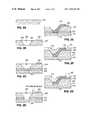
- FIG. 1Ashows a glass sheet that is to be used in the present invention
- FIG. 1Bshows the glass sheet shown in FIG. 1A after being prepared to be adhered to a semiconductor wafer
- FIG. 1Cshows the glass sheet shown in FIG. 1B adhered to a semiconductor wafer
- FIG. 1Dshows the completed glass sheet/semiconductor wafer structure
- FIG. 1Eshows an individual chip that has been sawn or cut from the glass sheet semiconductor structure of FIG. 1D .
- FIG. 2Ashows a cross-section of a portion of the glass sheet shown in FIG. 1A ;
- FIG. 2Bshows the portion of the cross-section of the glass sheet shown in FIG. 2A with a hole formed in the glass sheet and a pad formed on the surface of the glass sheet;
- FIG. 2Cshows the cross-section of the glass sheet shown in FIG. 2B after the glass sheet has been adhered to a semiconductor wafer as shown in FIG. 1C ;
- FIG. 2Dshows the glass sheet/semiconductor wafer structure as shown in FIG. 2C prepared for the formation of conductive traces from a bond pad on the semiconductor wafer to the pad on the glass sheet;
- FIG. 2Eshows the trace formed from the pad on the semiconductor wafer to the pad on the glass sheet
- FIG. 2Fshows the structure shown in FIG. 2E with a masking layer formed to allow formation of a solder ball on the pad on the glass sheet;
- FIG. 2Gshows the structure shown in FIG. 2F with the solder ball formed on the pad on the glass sheet
- FIG. 3Ashows a cross-section of a portion of the glass sheet shown in FIG. 1A ;
- FIG. 3Bshows the portion of the cross-section of the glass sheet shown in FIG. 3A with a hole formed in the glass sheet and a pad formed on the surface of the glass sheet with a portion of the pad extending down the sides of the hole in the glass sheet;
- FIG. 3Cshows the cross-section of the glass sheet shown in FIG. 3B after the glass sheet has been adhered to a semiconductor wafer as shown in FIG. 1C ;
- FIG. 3Dshows the glass sheet/semiconductor wafer structure as shown in FIG. 3C prepared for the formation of an interconnect material to the pad on the wafer;
- FIG. 3Eshows the structure shown in FIG. 3D with a masking layer formed to allow formation of a solder ball on the pad on the surface of the glass sheet;
- FIG. 3Fshows the structure shown in FIG. 3E with the solder ball formed on the pad on the glass sheet.
- FIGS. 1A–1Dillustrates how the structure of a glass sheet and semiconductor wafer is formed in accordance with the present invention and a resulting individual chip sawn or cut from the glass sheet/semiconductor wafer structure.
- FIG. 1Ashows a glass sheet 100 .
- the glass sheet 100is substantially the same size as the semiconductor wafer to which it will be adhered.
- the material of the glass sheetis made from a material having a coefficient of expansion that matches the coefficient of expansion of the semiconductor wafer to reduce the stress placed on the wafer due to temperature variations.
- the coefficient of expansion of the glass sheet materialcan be chosen to also reduce the stress placed on the interconnections to the next level of substrate.
- FIG. 1Bshows the glass sheet 100 with holes 102 etched into and through the glass sheet 100 . It should be appreciated that only a few of the many holes are shown in the surface of the glass sheet 100 .
- the holes 102are in a pattern that matches a pattern of bond pads on a semiconductor wafer to which the glass sheet is to be adhered.
- pads 104formed on the surface of the glass sheet 100 adjacent to the holes 102 . It should also be understood that only a few of the many pads are shown formed on the surface of the glass sheet 100 . The details of the holes 102 and pads 104 are discussed below.
- FIG. 1Cshows the glass sheet 100 adhered to a semiconductor wafer 106 by a layer 108 of adhesive.
- the glass sheet 100 and layer 108 of adhesiveprovide electrical insulation from the circuitry on the wafer 106 .
- FIG. 1Dshows the structure shown in FIG. 1C with the holes 102 filled with a conducting material 110 and solder balls 112 formed on the pads 104 .
- FIG. 1Eshows an individual chip that has been sawn or cut from the glass sheet semiconductor/structure shown in FIG. 1D . It should be understood that there are many more hole/solder ball structures on an actual chip 114 .
- FIGS. 2A–2Gillustrate a method of forming a glass sheet/semiconductor wafer structure according to a first embodiment of the present invention.
- FIG. 2Ashows a cross-section 200 of a portion of the glass sheet 100 shown in FIG. 1A .
- FIG. 2Bshows a hole (via) 202 etched through the portion of the glass sheet 200 .
- the hole 202can have tapered sides 204 and 206 or the sides can be non-tapered.
- the placement of the hole 202corresponds to a position of a bond pad that is formed on the wafer to which the glass sheet is to be adhered.
- a pad 208is formed on the surface of the glass sheet 200 adjacent to each hole 202 .
- the pad 208is formed from a metal such as aluminum or nickel.
- the glass sheet 200can be pre-metallized with other metals such as gold or copper.
- FIG. 2Cshows the portion of the glass sheet 200 adhered to a portion of a wafer 210 with a layer of adhesive 212 .
- a metallization pad 214is shown formed on the surface of the wafer 210 .
- the layer of adhesive 212is made from an epoxy that electrically insulates the circuitry on the wafer 210 and, in addition, provides stability to the glass sheet/semiconductor wafer structure.
- the layer of adhesive 212conforms to the surface of the semiconductor wafer with or without a passivation layer protecting the semiconductor wafer 210 from the glass sheet 200 .
- the layer of adhesive 212is sufficiently compliant to allow a slight mismatch in the coefficient of expansions of the glass sheet 200 and semiconductor wafer 210 thus reducing any stress placed on the semiconductor wafer by a temperature change.
- the electrical insulationcan be increased by increasing the thickness of the glass sheet and/or the thickness of the layer of adhesive 212 .
- the signal impedance of the devicecan be controlled by the selection of the glass material for the glass sheet 200 , the selection of the material for the metal pad 208 and by the selection of the layout design parameters.
- FIG. 2Dshows the structure shown in FIG. 2C with the layer of adhesive over bond pad 214 removed to allow access to the pad 214 .
- the adhesive over the pad 214is removed by a plasma etch process.
- FIG. 2Eshows the structure shown in FIG. 2D with a conductive trace 216 formed that electrically connects pad 208 to the bond pad 214 in the semiconductor wafer 210 .
- the conductive trace 216bridges the gap between the glass sheet 200 and the semiconductor wafer 210 created by the thickness of the layer of adhesive 212 .
- aluminumis utilized for metallization of bond pads 208 and therefore, deposition of aluminum with an etch removal of excess aluminum is the preferred method of obtaining the bridge metallization.
- Alternative methodsinclude, but are not limited to a mechanical application of metal such as gold or aluminum, metal plug application in the opening or the use of a conductive polymer such as an epoxy filled with a conductive material such as aluminum flakes.
- the conductive trace 216is typically aluminum.
- the pre-metallization of the glass sheet 200allows the use of different metals for the conductive trace 216 , pad 208 and the bond pad 214 .
- the use of a glass sheet 200allows the use of a metal for the conductive trace 216 that would otherwise require the use of a diffusion barrier layer between the semiconductor pad 214 and the conductive trace 216 on the glass sheet 200 without having to use a diffusion barrier layer.
- a typical processwould be to metallize the glass with copper or gold and then deposit aluminum in the opening 202 as the bridge or trace metal. Since aluminum is the most common bond pad material, the use of aluminum as a bridge or trace metal does not adversely affect the bond pad 214 and aluminum is compatible with whatever metal is used as the conductive trace 216 .
- FIG. 2Fshows the structure shown in FIG. 2E with a mask 218 formed on the surface of the structure shown in FIG. 2E .
- a hole 220is etched in the mask 218 over the pad 208 in order for a solder ball to be formed on the pad 208 .
- FIG. 2Gshows the structure shown in FIG. 2F with a solder ball 222 formed on the pad 208 .
- the solder ball 222allows attachment to a next level of interconnect and is a normal practice for chip scale packages and ball grid array packages.
- the solder ball 222is a tin and lead composition, however, other attachment materials can be used such as a metal bump or a polymer conductive bump.
- FIGS. 3A–3Gillustrate a method of forming a glass sheet/semiconductor wafer structure according to a second embodiment of the present invention.
- FIG. 3Ashows a cross-section 300 of a portion of the glass sheet 100 shown in FIG. 1A .
- FIG. 3Bshows a hole (via) 302 etched through the portion of the glass sheet 300 .
- the hole 302can have tapered sides 304 and 306 as shown or the sides can be non-tapered.
- the placement of the hole 302 in the glass sheet 300corresponds to a position of a pad that is formed on the wafer to which the glass sheet is to be adhered.
- a metal pad 308is formed on the surface of the glass sheet 300 and on the sides 304 and 306 of the hole 302 .
- a metal pad 308is formed as shown for each hole 302 .
- the metal pad 308is formed from a metal such as aluminum or nickel.
- the pad 308can be formed from other metals such as gold or copper.
- FIG. 3Cshows the portion of the glass sheet 300 adhered to a portion of a wafer 310 with a layer of adhesive 312 .
- a bond pad 314is shown formed on the surface of semiconductor wafer 310 .
- the layer of adhesive 312is an epoxy that electrically insulates the circuitry on the wafer 310 and, in addition, provides stability to the glass sheet/semiconductor wafer structure.
- the layer of adhesive 312conforms to the surface of the semiconductor wafer with or without a passivation layer protecting the wafer 310 from the glass sheet 300 .
- the layer of adhesive 312is sufficiently compliant to allow slight mismatch in the coefficient of expansions of glass sheet 200 and semiconductor wafer 310 thus reducing any stress placed on the semiconductor wafer by a temperature change.
- the electrical insulationcan be increased by increasing the thickness of the glass sheet and/or the thickness of the layer of adhesive 312 .
- the signal impedance of the devicecan be controlled by the selection of the glass material for the glass sheet 300 , the selection of the material for the metal pad 308 and by the selection of the layout design parameters.
- FIG. 3Dshows the structure shown in FIG. 3C with the layer of adhesive over the pad 314 removed to allow access to the bond pad 314 .
- the adhesive over the bond pad 314is removed by a plasma etch process.
- FIG. 3Eshows the structure shown in FIG. 3D with a metal plug 316 formed in the hole 302 .
- the metal plug 316electrically connects pad 308 to bond pad 314 in the semiconductor wafer 310 .
- the metal plug 316bridges the gap between the glass sheet 300 and the wafer 310 created by the thickness of the layer of adhesive 312 .
- aluminumis utilized for metallization of bond pads 308 and therefore, deposition of aluminum with an etch removal of excess aluminum is the preferred method of obtaining the plug metallization.
- Alternative methodsinclude, but are not limited to a mechanical application of metal such as gold or aluminum or the use of a conductive polymer such as an epoxy filled with a conductive material such as aluminum flakes.
- the pre-metallization of the glass sheet 300allows use of different metals for the metal plug 316 , pad 308 and the metal trace 316 .
- the use of glass sheet 300allows the use of a metal for the conductive plug 316 that would otherwise require the use of a diffusion barrier layer between the bond pad 314 and the metal pad 308 on the glass sheet 300 without having to use the diffusion barrier layer.
- a typical process, in this case,would be to metallize the glass with copper or gold and then deposit aluminum in the opening 302 as the plug material. Since aluminum is the most common bond pad material, the use of aluminum as the plug material does not adversely affect the bond pad 314 and aluminum is compatible with whatever metal is used as the metal pad 308 .
- FIG. 3Fshows the structure shown in FIG. 3E with a mask 318 formed on the surface of the structure shown in FIG. 3E .
- a hole 320is etched in the mask 318 over a portion of the pad 308 in order for a solder ball to be formed on the pad 318 .
- FIG. 3Gshows the structure shown in FIG. 3F with a solder ball 322 formed on the pad 308 .
- the solder ball 322allows attachment to a next level of interconnect and is a normal practice for chip scale packages and ball grid array packages.
- the solder ball 322is a tin and lead composition, however, other attachment materials can be used such as a metal bump or a polymer conductive bump.
Landscapes
- Engineering & Computer Science (AREA)
- Microelectronics & Electronic Packaging (AREA)
- Computer Hardware Design (AREA)
- Power Engineering (AREA)
- Physics & Mathematics (AREA)
- Condensed Matter Physics & Semiconductors (AREA)
- General Physics & Mathematics (AREA)
- Manufacturing & Machinery (AREA)
- Internal Circuitry In Semiconductor Integrated Circuit Devices (AREA)
Abstract
Description
Claims (10)
Priority Applications (6)
| Application Number | Priority Date | Filing Date | Title |
|---|---|---|---|
| US09/045,507US7215025B1 (en) | 1998-03-20 | 1998-03-20 | Wafer scale semiconductor structure |
| US09/686,016US6555469B1 (en) | 1998-03-20 | 2000-10-10 | Chip scale packages |
| US10/190,055US6982475B1 (en) | 1998-03-20 | 2002-07-03 | Hermetic wafer scale integrated circuit structure |
| US10/224,197US6753208B1 (en) | 1998-03-20 | 2002-08-19 | Wafer scale method of packaging integrated circuit die |
| US11/250,821US7205181B1 (en) | 1998-03-20 | 2005-10-14 | Method of forming hermetic wafer scale integrated circuit structure |
| US11/250,823US7205635B1 (en) | 1998-03-20 | 2005-10-14 | Hermetic wafer scale integrated circuit structure |
Applications Claiming Priority (1)
| Application Number | Priority Date | Filing Date | Title |
|---|---|---|---|
| US09/045,507US7215025B1 (en) | 1998-03-20 | 1998-03-20 | Wafer scale semiconductor structure |
Related Parent Applications (2)
| Application Number | Title | Priority Date | Filing Date |
|---|---|---|---|
| US09/045,507DivisionUS7215025B1 (en) | 1998-03-20 | 1998-03-20 | Wafer scale semiconductor structure |
| US09/686,016Continuation-In-PartUS6555469B1 (en) | 1998-03-20 | 2000-10-10 | Chip scale packages |
Related Child Applications (4)
| Application Number | Title | Priority Date | Filing Date |
|---|---|---|---|
| US09/045,507DivisionUS7215025B1 (en) | 1998-03-20 | 1998-03-20 | Wafer scale semiconductor structure |
| US09/686,016Continuation-In-PartUS6555469B1 (en) | 1998-03-20 | 2000-10-10 | Chip scale packages |
| US09/686,016DivisionUS6555469B1 (en) | 1998-03-20 | 2000-10-10 | Chip scale packages |
| US10/190,055Continuation-In-PartUS6982475B1 (en) | 1998-03-20 | 2002-07-03 | Hermetic wafer scale integrated circuit structure |
Publications (1)
| Publication Number | Publication Date |
|---|---|
| US7215025B1true US7215025B1 (en) | 2007-05-08 |
Family
ID=21938288
Family Applications (2)
| Application Number | Title | Priority Date | Filing Date |
|---|---|---|---|
| US09/045,507Expired - Fee RelatedUS7215025B1 (en) | 1998-03-20 | 1998-03-20 | Wafer scale semiconductor structure |
| US09/686,016Expired - LifetimeUS6555469B1 (en) | 1998-03-20 | 2000-10-10 | Chip scale packages |
Family Applications After (1)
| Application Number | Title | Priority Date | Filing Date |
|---|---|---|---|
| US09/686,016Expired - LifetimeUS6555469B1 (en) | 1998-03-20 | 2000-10-10 | Chip scale packages |
Country Status (1)
| Country | Link |
|---|---|
| US (2) | US7215025B1 (en) |
Cited By (4)
| Publication number | Priority date | Publication date | Assignee | Title |
|---|---|---|---|---|
| US20050230843A1 (en)* | 2000-02-24 | 2005-10-20 | Williams Vernon M | Flip-chip type semiconductor devices and conductive elements thereof |
| US20060012024A1 (en)* | 2000-10-13 | 2006-01-19 | Bridge Semiconductor Corporation | Semiconductor chip assembly with metal containment wall and solder terminal |
| US10115671B2 (en) | 2012-08-03 | 2018-10-30 | Snaptrack, Inc. | Incorporation of passives and fine pitch through via for package on package |
| CN115274460A (en)* | 2021-04-30 | 2022-11-01 | 长鑫存储技术有限公司 | Semiconductor structure, manufacturing method thereof and wafer bonding method |
Families Citing this family (9)
| Publication number | Priority date | Publication date | Assignee | Title |
|---|---|---|---|---|
| US20020076854A1 (en)* | 2000-12-15 | 2002-06-20 | Pierce John L. | System, method and apparatus for constructing a semiconductor wafer-interposer using B-Stage laminates |
| US7498196B2 (en)* | 2001-03-30 | 2009-03-03 | Megica Corporation | Structure and manufacturing method of chip scale package |
| TW544882B (en) | 2001-12-31 | 2003-08-01 | Megic Corp | Chip package structure and process thereof |
| TW503496B (en) | 2001-12-31 | 2002-09-21 | Megic Corp | Chip packaging structure and manufacturing process of the same |
| TW584950B (en) | 2001-12-31 | 2004-04-21 | Megic Corp | Chip packaging structure and process thereof |
| US6673698B1 (en) | 2002-01-19 | 2004-01-06 | Megic Corporation | Thin film semiconductor package utilizing a glass substrate with composite polymer/metal interconnect layers |
| JP4405865B2 (en)* | 2004-06-24 | 2010-01-27 | 富士通マイクロエレクトロニクス株式会社 | Multilayer wiring structure manufacturing method and FIB apparatus |
| US20060138626A1 (en)* | 2004-12-29 | 2006-06-29 | Tessera, Inc. | Microelectronic packages using a ceramic substrate having a window and a conductive surface region |
| CN118943122B (en)* | 2024-07-23 | 2025-04-29 | 东莞锐信仪器有限公司 | Semiconductor packaging structure, substrate, device and manufacturing method |
Citations (8)
| Publication number | Priority date | Publication date | Assignee | Title |
|---|---|---|---|---|
| US5258648A (en)* | 1991-06-27 | 1993-11-02 | Motorola, Inc. | Composite flip chip semiconductor device with an interposer having test contacts formed along its periphery |
| US5468681A (en)* | 1989-08-28 | 1995-11-21 | Lsi Logic Corporation | Process for interconnecting conductive substrates using an interposer having conductive plastic filled vias |
| US5705858A (en)* | 1993-04-14 | 1998-01-06 | Nec Corporation | Packaging structure for a hermetically sealed flip chip semiconductor device |
| US5814894A (en)* | 1995-04-07 | 1998-09-29 | Nitto Denko Corporation | Semiconductor device, production method thereof, and tape carrier for semiconductor device used for producing the semiconductor device |
| US5844304A (en)* | 1994-09-30 | 1998-12-01 | Nec Corporation | Process for manufacturing semiconductor device and semiconductor wafer |
| US5973337A (en)* | 1997-08-25 | 1999-10-26 | Motorola, Inc. | Ball grid device with optically transmissive coating |
| US6300235B1 (en)* | 1997-06-30 | 2001-10-09 | Siemens Aktiengesellschaft | Method of forming multi-level coplanar metal/insulator films using dual damascene with sacrificial flowable oxide |
| US6303977B1 (en) | 1998-12-03 | 2001-10-16 | Texas Instruments Incorporated | Fully hermetic semiconductor chip, including sealed edge sides |
Family Cites Families (1)
| Publication number | Priority date | Publication date | Assignee | Title |
|---|---|---|---|---|
| US4246595A (en)* | 1977-03-08 | 1981-01-20 | Matsushita Electric Industrial Co., Ltd. | Electronics circuit device and method of making the same |
- 1998
- 1998-03-20USUS09/045,507patent/US7215025B1/ennot_activeExpired - Fee Related
- 2000
- 2000-10-10USUS09/686,016patent/US6555469B1/ennot_activeExpired - Lifetime
Patent Citations (8)
| Publication number | Priority date | Publication date | Assignee | Title |
|---|---|---|---|---|
| US5468681A (en)* | 1989-08-28 | 1995-11-21 | Lsi Logic Corporation | Process for interconnecting conductive substrates using an interposer having conductive plastic filled vias |
| US5258648A (en)* | 1991-06-27 | 1993-11-02 | Motorola, Inc. | Composite flip chip semiconductor device with an interposer having test contacts formed along its periphery |
| US5705858A (en)* | 1993-04-14 | 1998-01-06 | Nec Corporation | Packaging structure for a hermetically sealed flip chip semiconductor device |
| US5844304A (en)* | 1994-09-30 | 1998-12-01 | Nec Corporation | Process for manufacturing semiconductor device and semiconductor wafer |
| US5814894A (en)* | 1995-04-07 | 1998-09-29 | Nitto Denko Corporation | Semiconductor device, production method thereof, and tape carrier for semiconductor device used for producing the semiconductor device |
| US6300235B1 (en)* | 1997-06-30 | 2001-10-09 | Siemens Aktiengesellschaft | Method of forming multi-level coplanar metal/insulator films using dual damascene with sacrificial flowable oxide |
| US5973337A (en)* | 1997-08-25 | 1999-10-26 | Motorola, Inc. | Ball grid device with optically transmissive coating |
| US6303977B1 (en) | 1998-12-03 | 2001-10-16 | Texas Instruments Incorporated | Fully hermetic semiconductor chip, including sealed edge sides |
Cited By (5)
| Publication number | Priority date | Publication date | Assignee | Title |
|---|---|---|---|---|
| US20050230843A1 (en)* | 2000-02-24 | 2005-10-20 | Williams Vernon M | Flip-chip type semiconductor devices and conductive elements thereof |
| US20060012024A1 (en)* | 2000-10-13 | 2006-01-19 | Bridge Semiconductor Corporation | Semiconductor chip assembly with metal containment wall and solder terminal |
| US7414319B2 (en)* | 2000-10-13 | 2008-08-19 | Bridge Semiconductor Corporation | Semiconductor chip assembly with metal containment wall and solder terminal |
| US10115671B2 (en) | 2012-08-03 | 2018-10-30 | Snaptrack, Inc. | Incorporation of passives and fine pitch through via for package on package |
| CN115274460A (en)* | 2021-04-30 | 2022-11-01 | 长鑫存储技术有限公司 | Semiconductor structure, manufacturing method thereof and wafer bonding method |
Also Published As
| Publication number | Publication date |
|---|---|
| US6555469B1 (en) | 2003-04-29 |
Similar Documents
| Publication | Publication Date | Title |
|---|---|---|
| US6753208B1 (en) | Wafer scale method of packaging integrated circuit die | |
| US8535976B2 (en) | Method for fabricating chip package with die and substrate | |
| US7218005B2 (en) | Compact semiconductor device capable of mounting a plurality of semiconductor chips with high density and method of manufacturing the same | |
| US9136246B2 (en) | Integrated chip package structure using silicon substrate and method of manufacturing the same | |
| US7898058B2 (en) | Integrated chip package structure using organic substrate and method of manufacturing the same | |
| US5918364A (en) | Method of forming electrically conductive polymer interconnects on electrical substrates | |
| US7173330B2 (en) | Multiple chip semiconductor package | |
| US7511376B2 (en) | Circuitry component with metal layer over die and extending to place not over die | |
| US6410406B1 (en) | Semiconductor device including edge bond pads and methods | |
| US7750467B2 (en) | Chip scale package structure with metal pads exposed from an encapsulant | |
| US6495912B1 (en) | Structure of ceramic package with integrated passive devices | |
| US20080119029A1 (en) | Wafer scale thin film package | |
| CN101276809A (en) | Semiconductor device and manufacturing method thereof | |
| JP3651346B2 (en) | Semiconductor device and manufacturing method thereof | |
| US20090008777A1 (en) | Inter-connecting structure for semiconductor device package and method of the same | |
| US7215025B1 (en) | Wafer scale semiconductor structure | |
| US9324681B2 (en) | Pin attachment | |
| US20050258536A1 (en) | Chip heat sink device and method | |
| KR20090041988A (en) | Manufacturing method of chip on chip semiconductor device |
Legal Events
| Date | Code | Title | Description |
|---|---|---|---|
| AS | Assignment | Owner name:MICROCSP, INC., CALIFORNIA Free format text:ASSIGNMENT OF ASSIGNORS INTEREST;ASSIGNOR:MACINTYRE, DONALD MALCOLM;REEL/FRAME:011233/0226 Effective date:20001003 | |
| AS | Assignment | Owner name:MCSP, LLC, CALIFORNIA Free format text:ASSIGNMENT OF ASSIGNORS INTEREST;ASSIGNOR:MICROCSP, INC.;REEL/FRAME:014949/0376 Effective date:20040129 | |
| STCF | Information on status: patent grant | Free format text:PATENTED CASE | |
| AS | Assignment | Owner name:MICRO CHIP SCALE PACKAGING, INC., CALIFORNIA Free format text:ASSIGNMENT OF ASSIGNORS INTEREST;ASSIGNOR:MCSP, LLC;REEL/FRAME:021147/0609 Effective date:20080619 | |
| FPAY | Fee payment | Year of fee payment:4 | |
| REMI | Maintenance fee reminder mailed | ||
| FPAY | Fee payment | Year of fee payment:8 | |
| SULP | Surcharge for late payment | Year of fee payment:7 | |
| FEPP | Fee payment procedure | Free format text:MAINTENANCE FEE REMINDER MAILED (ORIGINAL EVENT CODE: REM.); ENTITY STATUS OF PATENT OWNER: SMALL ENTITY | |
| LAPS | Lapse for failure to pay maintenance fees | Free format text:PATENT EXPIRED FOR FAILURE TO PAY MAINTENANCE FEES (ORIGINAL EVENT CODE: EXP.); ENTITY STATUS OF PATENT OWNER: SMALL ENTITY | |
| STCH | Information on status: patent discontinuation | Free format text:PATENT EXPIRED DUE TO NONPAYMENT OF MAINTENANCE FEES UNDER 37 CFR 1.362 | |
| FP | Lapsed due to failure to pay maintenance fee | Effective date:20190508 |