US7214958B2 - Phase change memory cell with high read margin at low power operation - Google Patents
Phase change memory cell with high read margin at low power operationDownload PDFInfo
- Publication number
- US7214958B2 US7214958B2US11/101,972US10197205AUS7214958B2US 7214958 B2US7214958 B2US 7214958B2US 10197205 AUS10197205 AUS 10197205AUS 7214958 B2US7214958 B2US 7214958B2
- Authority
- US
- United States
- Prior art keywords
- phase
- change material
- memory cell
- change
- layer
- Prior art date
- Legal status (The legal status is an assumption and is not a legal conclusion. Google has not performed a legal analysis and makes no representation as to the accuracy of the status listed.)
- Expired - Fee Related
Links
- 230000015654memoryEffects0.000titleclaimsabstractdescription95
- 230000008859changeEffects0.000titledescription9
- 239000012782phase change materialSubstances0.000claimsabstractdescription139
- 239000000463materialSubstances0.000claimsabstractdescription112
- 238000002955isolationMethods0.000claimsabstractdescription73
- 238000009792diffusion processMethods0.000claimsabstractdescription66
- 230000004888barrier functionEffects0.000claimsabstractdescription65
- 239000003989dielectric materialSubstances0.000claimsdescription9
- 229910000618GeSbTeInorganic materials0.000claimsdescription3
- 150000004770chalcogenidesChemical class0.000claimsdescription3
- 239000007772electrode materialSubstances0.000description35
- 238000000151depositionMethods0.000description15
- 238000005530etchingMethods0.000description15
- 238000000034methodMethods0.000description14
- 238000002844meltingMethods0.000description10
- 230000008018meltingEffects0.000description10
- 238000005229chemical vapour depositionMethods0.000description8
- 239000012212insulatorSubstances0.000description8
- 238000000231atomic layer depositionMethods0.000description7
- 238000001912gas jet depositionMethods0.000description7
- VYPSYNLAJGMNEJ-UHFFFAOYSA-NSilicium dioxideChemical compoundO=[Si]=OVYPSYNLAJGMNEJ-UHFFFAOYSA-N0.000description6
- 230000008021depositionEffects0.000description6
- 238000010438heat treatmentMethods0.000description6
- 230000008569processEffects0.000description6
- ATJFFYVFTNAWJD-UHFFFAOYSA-NTinChemical compound[Sn]ATJFFYVFTNAWJD-UHFFFAOYSA-N0.000description5
- 239000012774insulation materialSubstances0.000description5
- 229920002120photoresistant polymerPolymers0.000description5
- 238000009826distributionMethods0.000description4
- 239000011810insulating materialSubstances0.000description4
- -1chalcogenide compoundChemical class0.000description3
- 230000006870functionEffects0.000description3
- 238000010791quenchingMethods0.000description3
- 239000000377silicon dioxideSubstances0.000description3
- 239000000126substanceSubstances0.000description3
- RYGMFSIKBFXOCR-UHFFFAOYSA-NCopperChemical compound[Cu]RYGMFSIKBFXOCR-UHFFFAOYSA-N0.000description2
- 239000004964aerogelSubstances0.000description2
- 238000001816coolingMethods0.000description2
- 229910052802copperInorganic materials0.000description2
- 239000010949copperSubstances0.000description2
- 238000002425crystallisationMethods0.000description2
- 230000008025crystallizationEffects0.000description2
- 238000010586diagramMethods0.000description2
- 238000011049fillingMethods0.000description2
- 238000001465metallisationMethods0.000description2
- 238000005498polishingMethods0.000description2
- 235000012239silicon dioxideNutrition0.000description2
- 238000003860storageMethods0.000description2
- 230000007704transitionEffects0.000description2
- WFKWXMTUELFFGS-UHFFFAOYSA-NtungstenChemical compound[W]WFKWXMTUELFFGS-UHFFFAOYSA-N0.000description2
- 229910052721tungstenInorganic materials0.000description2
- 239000010937tungstenSubstances0.000description2
- 229910000763AgInSbTeInorganic materials0.000description1
- 229910005542GaSbInorganic materials0.000description1
- 229910005872GeSbInorganic materials0.000description1
- 244000208734Pisonia aculeataSpecies0.000description1
- 230000006978adaptationEffects0.000description1
- 229910045601alloyInorganic materials0.000description1
- 239000000956alloySubstances0.000description1
- 229910052681coesiteInorganic materials0.000description1
- 229910052906cristobaliteInorganic materials0.000description1
- 238000001035dryingMethods0.000description1
- 238000009413insulationMethods0.000description1
- 238000004519manufacturing processMethods0.000description1
- 239000000155meltSubstances0.000description1
- 229910052751metalInorganic materials0.000description1
- 239000002184metalSubstances0.000description1
- 238000013021overheatingMethods0.000description1
- 230000000737periodic effectEffects0.000description1
- 238000000206photolithographyMethods0.000description1
- 229920000642polymerPolymers0.000description1
- 230000009467reductionEffects0.000description1
- 230000006903response to temperatureEffects0.000description1
- 238000004528spin coatingMethods0.000description1
- 229910052682stishoviteInorganic materials0.000description1
- 229910052905tridymiteInorganic materials0.000description1
- 238000009966trimmingMethods0.000description1
- 238000007740vapor depositionMethods0.000description1
Images


Classifications
- H—ELECTRICITY
- H10—SEMICONDUCTOR DEVICES; ELECTRIC SOLID-STATE DEVICES NOT OTHERWISE PROVIDED FOR
- H10N—ELECTRIC SOLID-STATE DEVICES NOT OTHERWISE PROVIDED FOR
- H10N70/00—Solid-state devices having no potential barriers, and specially adapted for rectifying, amplifying, oscillating or switching
- H10N70/20—Multistable switching devices, e.g. memristors
- H10N70/231—Multistable switching devices, e.g. memristors based on solid-state phase change, e.g. between amorphous and crystalline phases, Ovshinsky effect
- G—PHYSICS
- G11—INFORMATION STORAGE
- G11C—STATIC STORES
- G11C13/00—Digital stores characterised by the use of storage elements not covered by groups G11C11/00, G11C23/00, or G11C25/00
- G11C13/0002—Digital stores characterised by the use of storage elements not covered by groups G11C11/00, G11C23/00, or G11C25/00 using resistive RAM [RRAM] elements
- G11C13/0004—Digital stores characterised by the use of storage elements not covered by groups G11C11/00, G11C23/00, or G11C25/00 using resistive RAM [RRAM] elements comprising amorphous/crystalline phase transition cells
- G—PHYSICS
- G11—INFORMATION STORAGE
- G11C—STATIC STORES
- G11C13/00—Digital stores characterised by the use of storage elements not covered by groups G11C11/00, G11C23/00, or G11C25/00
- G11C13/0002—Digital stores characterised by the use of storage elements not covered by groups G11C11/00, G11C23/00, or G11C25/00 using resistive RAM [RRAM] elements
- G11C13/0021—Auxiliary circuits
- G11C13/0069—Writing or programming circuits or methods
- H—ELECTRICITY
- H10—SEMICONDUCTOR DEVICES; ELECTRIC SOLID-STATE DEVICES NOT OTHERWISE PROVIDED FOR
- H10N—ELECTRIC SOLID-STATE DEVICES NOT OTHERWISE PROVIDED FOR
- H10N70/00—Solid-state devices having no potential barriers, and specially adapted for rectifying, amplifying, oscillating or switching
- H10N70/011—Manufacture or treatment of multistable switching devices
- H10N70/061—Shaping switching materials
- H10N70/063—Shaping switching materials by etching of pre-deposited switching material layers, e.g. lithography
- H—ELECTRICITY
- H10—SEMICONDUCTOR DEVICES; ELECTRIC SOLID-STATE DEVICES NOT OTHERWISE PROVIDED FOR
- H10N—ELECTRIC SOLID-STATE DEVICES NOT OTHERWISE PROVIDED FOR
- H10N70/00—Solid-state devices having no potential barriers, and specially adapted for rectifying, amplifying, oscillating or switching
- H10N70/011—Manufacture or treatment of multistable switching devices
- H10N70/061—Shaping switching materials
- H10N70/066—Shaping switching materials by filling of openings, e.g. damascene method
- H—ELECTRICITY
- H10—SEMICONDUCTOR DEVICES; ELECTRIC SOLID-STATE DEVICES NOT OTHERWISE PROVIDED FOR
- H10N—ELECTRIC SOLID-STATE DEVICES NOT OTHERWISE PROVIDED FOR
- H10N70/00—Solid-state devices having no potential barriers, and specially adapted for rectifying, amplifying, oscillating or switching
- H10N70/801—Constructional details of multistable switching devices
- H10N70/821—Device geometry
- H10N70/826—Device geometry adapted for essentially vertical current flow, e.g. sandwich or pillar type devices
- H—ELECTRICITY
- H10—SEMICONDUCTOR DEVICES; ELECTRIC SOLID-STATE DEVICES NOT OTHERWISE PROVIDED FOR
- H10N—ELECTRIC SOLID-STATE DEVICES NOT OTHERWISE PROVIDED FOR
- H10N70/00—Solid-state devices having no potential barriers, and specially adapted for rectifying, amplifying, oscillating or switching
- H10N70/801—Constructional details of multistable switching devices
- H10N70/841—Electrodes
- H10N70/8413—Electrodes adapted for resistive heating
- H—ELECTRICITY
- H10—SEMICONDUCTOR DEVICES; ELECTRIC SOLID-STATE DEVICES NOT OTHERWISE PROVIDED FOR
- H10N—ELECTRIC SOLID-STATE DEVICES NOT OTHERWISE PROVIDED FOR
- H10N70/00—Solid-state devices having no potential barriers, and specially adapted for rectifying, amplifying, oscillating or switching
- H10N70/801—Constructional details of multistable switching devices
- H10N70/861—Thermal details
- H10N70/8616—Thermal insulation means
- H—ELECTRICITY
- H10—SEMICONDUCTOR DEVICES; ELECTRIC SOLID-STATE DEVICES NOT OTHERWISE PROVIDED FOR
- H10N—ELECTRIC SOLID-STATE DEVICES NOT OTHERWISE PROVIDED FOR
- H10N70/00—Solid-state devices having no potential barriers, and specially adapted for rectifying, amplifying, oscillating or switching
- H10N70/801—Constructional details of multistable switching devices
- H10N70/881—Switching materials
- H10N70/882—Compounds of sulfur, selenium or tellurium, e.g. chalcogenides
- H10N70/8828—Tellurides, e.g. GeSbTe
- H—ELECTRICITY
- H10—SEMICONDUCTOR DEVICES; ELECTRIC SOLID-STATE DEVICES NOT OTHERWISE PROVIDED FOR
- H10N—ELECTRIC SOLID-STATE DEVICES NOT OTHERWISE PROVIDED FOR
- H10N70/00—Solid-state devices having no potential barriers, and specially adapted for rectifying, amplifying, oscillating or switching
- H10N70/801—Constructional details of multistable switching devices
- H10N70/881—Switching materials
- H10N70/884—Switching materials based on at least one element of group IIIA, IVA or VA, e.g. elemental or compound semiconductors
- G—PHYSICS
- G11—INFORMATION STORAGE
- G11C—STATIC STORES
- G11C13/00—Digital stores characterised by the use of storage elements not covered by groups G11C11/00, G11C23/00, or G11C25/00
- G11C13/0002—Digital stores characterised by the use of storage elements not covered by groups G11C11/00, G11C23/00, or G11C25/00 using resistive RAM [RRAM] elements
- G11C13/0021—Auxiliary circuits
- G11C13/0069—Writing or programming circuits or methods
- G11C2013/008—Write by generating heat in the surroundings of the memory material, e.g. thermowrite
- G—PHYSICS
- G11—INFORMATION STORAGE
- G11C—STATIC STORES
- G11C2213/00—Indexing scheme relating to G11C13/00 for features not covered by this group
- G11C2213/50—Resistive cell structure aspects
- G11C2213/52—Structure characterized by the electrode material, shape, etc.
Definitions
- phase-change memoriesrelate to phase-change memories.
- a system and methodare provided for a phase-change memory cell having a host material adjacent phase-change material such that heat leakage in the phase-change material is reduced.
- Phase-change materialsmay exhibit at least two different states. Consequently, phase-change material may be used in a memory cell to store a bit of data.
- the states of phase-change materialmay be referenced to as amorphous and crystalline states. The states may be distinguished because the amorphous state generally exhibits higher resistivity than does the crystalline state. Generally, the amorphous state involves a more disordered atomic structure, while the crystalline state is an ordered lattice.
- Phase change in the phase-change materialsmay be induced reversibly.
- the memorymay change from the amorphous to the crystalline state, and visa versa, in response to temperature changes.
- the temperature changes to the phase-change materialmay be achieved in a variety of ways.
- a lasercan be directed to the phase-change material, current may be driven through the phase-change material, or current or voltage can be fed through a resistive heater adjacent the phase-change material.
- controllable heating of the phase-change materialcauses controllable phase change within the phase-change material.
- phase-change memorycomprises a memory array having a plurality of memory cells that are made of phase-change material
- the memorymay be programmed to store data utilizing the memory states of the phase-change material.
- One way to read and write data in such a phase-change memory deviceis to control a current and/or a voltage pulse that is applied to the phase-change material.
- the level of current and voltagegenerally corresponds to the temperature induced within the phase-change material in each memory cell. In order to minimize the amount of power that is required in each memory cell, the amount of heat that leaks from the phase-change material should be minimized.
- the memory cell deviceincludes a first electrode, phase-change material adjacent the first electrode, a second electrode adjacent the phase-change material, a diffusion barrier adjacent the phase-change material, and isolation material adjacent the diffusion barrier for thermally isolating the phase-change material.
- the diffusion barrierprevents diffusion of the phase-change material into the isolation material.
- FIG. 1illustrates a block diagram of a memory cell device.
- FIG. 2illustrates a cross-sectional view through a phase-change memory cell.
- FIG. 3illustrates a cross-sectional view through a phase-change memory cell with an illustrated temperature contour plot during a reset operation.
- FIG. 4illustrates a cross-sectional view through a phase-change memory cell with a laterally surrounding isolation material in accordance with one embodiment of the present invention.
- FIG. 5illustrates a cross-sectional view through a phase-change memory cell with a laterally surrounding isolation material in accordance with another embodiment of the present invention.
- FIG. 6illustrates a graph plotting the cell resistance as obtained during a read operation as a function of the reset pulse voltage and current.
- FIG. 7illustrates a cross-sectional view through a phase-change memory cell with a laterally surrounding diffusion barrier and isolation material in accordance with another embodiment of the present invention.
- FIG. 8illustrates a cross-sectional view of one embodiment of a preprocessed wafer.
- FIG. 9illustrates a cross-sectional view of one embodiment of the preprocessed wafer, a phase-change material layer, and an electrode material layer.
- FIG. 10illustrates a cross-sectional view of one embodiment of the preprocessed wafer, phase-change material layer, electrode material layer, and a sublithographic mask layer.
- FIG. 11illustrates a cross-sectional view of one embodiment of the preprocessed wafer, phase-change material layer, and electrode material layer after etching the electrode material layer and the phase-change material layer.
- FIG. 12illustrates a cross-sectional view of one embodiment of the preprocessed wafer, phase-change material layer, electrode material layer, a diffusion barrier layer, and an isolation material layer.
- FIG. 13illustrates a cross-sectional view of one embodiment of the preprocessed wafer, phase-change material layer, electrode material layer, diffusion barrier layer, and isolation material layer after planarization.
- FIG. 14illustrates a cross-sectional view of one embodiment of the preprocessed wafer, phase-change material layer, electrode material layer, diffusion barrier layer, isolation material layer, and an additional electrode material layer after etching the additional electrode material layer.
- FIG. 15illustrates a cross-sectional view through a phase-change memory cell with a laterally surrounding diffusion barrier and isolation material in accordance with another embodiment of the present invention.
- FIG. 16illustrates a cross-sectional view of one embodiment of a preprocessed wafer.
- FIG. 17illustrates a cross-sectional view of one embodiment of the preprocessed wafer, an isolation material layer, a stop layer, and a sacrificial layer.
- FIG. 18illustrates a cross-sectional view of one embodiment of the preprocessed wafer, isolation material layer, stop layer, sacrificial layer, and a mask layer after etching the sacrificial layer.
- FIG. 19illustrates a cross-sectional view of one embodiment of the preprocessed wafer, isolation material layer, stop layer, sacrificial layer, and mask layer after etching the stop layer and the isolation material layer.
- FIG. 20illustrates a cross-sectional view one embodiment of the preprocessed wafer, isolation material layer, and stop layer after removing the mask layer and the sacrificial layer.
- FIG. 21illustrates a cross-sectional view of one embodiment of the preprocessed wafer, isolation material layer, and a diffusion barrier layer after etching the diffusion barrier layer.
- FIG. 22illustrates a cross-sectional view of one embodiment of the preprocessed wafer, isolation material layer, diffusion barrier layer, and a phase-change material layer.
- FIG. 23illustrates a cross-sectional view of one embodiment of the preprocessed wafer, isolation material layer, diffusion barrier layer, and phase-change material layer after planarization.
- FIG. 24illustrates a cross-sectional view of one embodiment of the preprocessed wafer, isolation material layer, diffusion barrier layer, phase-change material layer, and second electrode after etching the electrode material layer.
- FIG. 1illustrates a block diagram of a memory cell device 5 .
- Memory cell device 5includes write pulse generator 6 , distribution circuit 7 , and memory cells 8 a , 8 b , 8 c , and 8 d and a sense amplifier 9 .
- memory cells 8 a – 8 dare phase-change memory cells that are based on the amorphous to crystalline phase transition of the memory material.
- write pulse generator 6generates current or voltage pulses that are controllable directed to memory cells 8 a – 8 d via distribution circuit 7 .
- distribution circuit 7is a plurality of transistors that controllable direct current or voltage pulses to the memory, and in another embodiment, is a plurality of transistors that controllable direct current or voltage pulses to heaters adjacent to the phase-change memory cells.
- memory cells 8 a – 8 dare made of a phase-change material that may be changed from an amorphous state to a crystalline state or crystalline state to amorphous under influence of temperature change.
- the degree of crystallinitythereby defines at least two memory states for storing data within memory cell device 5 , which can be assigned to the bit values “0” and “1”.
- the bit states of memory cells 8 a – 8 ddiffer significantly in their electrical resistivity. In the amorphous state, a phase-change material will exhibit significantly higher resistivity than it will in the crystalline state. In this way, sense amplifier 9 may read the cell resistance such that the bit value assigned to a particular memory cell 8 a – 8 d can be determined.
- write pulse generator 6In order to program a memory cell 8 a – 8 d within memory cell device 5 , write pulse generator 6 generates a current or voltage pulse for heating the phase-change material in the target memory cell. In one embodiment, write pulse generator 6 generates an appropriate current or voltage pulse, which is fed into distribution circuit 7 and distributed to the appropriate target memory cell 8 a – 8 d . The current or voltage pulse amplitude and duration is controlled depending on whether the memory cell is being set or reset. Generally, a “set” operation of a memory cell is heating the phase-change material of the target memory cell above its crystallization temperature (but below its melting temperature) long enough to achieve the crystalline state. Generally, a “reset” operation of a memory cell is quickly heating the phase-change material of the target memory cell above its melting temperature, and then quickly quench cooling the material, thereby achieving the amorphous state.
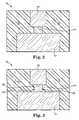
- FIG. 2illustrates a cross-section view through an exemplary phase-change memory cell 10 of the active-in-via type.
- Phase-change memory cell 10includes first electrode 12 , phase-change material 14 , second electrode 16 , and insulator material 18 .
- the phase change material 14is laterally completely enclosed by insulation material 18 , which defines the current path and hence the location of the phase change region in phase change material 14 .
- a selection devicesuch as an active device like a transistor or diode, may be coupled to first electrode 12 to control the application of current or voltage to first electrode 12 , and thus to phase-change material 14 , in order to set and reset phase-change material 14 .
- phase-change material 14a set current or voltage pulse is selectively enabled to phase-change material 14 thereby heating it above its crystallization temperature (but below its melting temperature). In this way, phase-change material 14 reaches its crystalline state during this set operation.
- a reset current and/or voltage pulseis selectively enabled by the selection device and sent through first electrode 12 to phase-change material 14 . The reset current or voltage quickly heats phase-change material 14 above its melting temperature, and then phase-change material 14 is quickly quench cooled to achieve its amorphous state.
- phase-change material 14typically begins heating and changing phases (melting) from the center of the cell due to thermal self-isolation of the phase-change material 14 . Generated heat, however, may also diffuse into insulator material 18 , which is typically an insulator material like silicon dioxide. Thus, in a low power reset operation, which avoids excessive overheating of the center, there is a crystalline, ring-shaped volume at the edge of phase-change material 14 remaining in the crystalline state due to incomplete melting. Such an incomplete melted area 22 is illustrated in FIG. 3 , surrounding a sufficiently melted area 20 in phase-change material 14 . A read operation undertaken subsequent to a reset in such a configuration provides low resistance shunt current paths in the area 22 . This will mask the readout signal detected by sense amplifier 9 in the high resistance state.
- FIG. 4illustrates a cross-section view through an exemplary phase-change memory cell 30 in accordance with one embodiment of the present invention.
- Phase-change memory cell 30includes first electrode 32 , phase-change material 34 , second electrode 36 , and insulator material 38 .
- phase-change memory cell 30includes isolation material 40 adjacent phase-change material 34 .
- isolation material 40is selected to have low thermal conductivity/diffusivity, thereby reducing the heat leakage from the edges of phase-change material 34 .
- phase-change memory cell 30is an active-in-via (AIV) cell such that a reset pulse typically melts phase-change material 34 starting at its center, and then the melting front moves outward.
- isolation material 40surrounds phase-change material 34 at its outer edges. This reduces heat leakage from the edge of phase-change material 34 by the improved thermal insulation provided by the surrounding isolation material 40 . In this way, unlike with phase-change memory device 10 , melting of phase-change material 34 during a low power reset operation tends to go all the way out to its edge, thereby avoiding the crystalline, ring-shaped volume found in the prior embodiment.
- phase-change material 34Since even the outermost portions phase-change material 34 are melted (and subsequently amorphized during quench cooling), the total cell resistance will be much higher and read operation undertaken subsequent to a reset provides large read signals detected by sense amplifier 9 . In this way, less input power is needed to achieve adequate read margins during reset operations. This allows lowering the reset pulse signal compared to a cell without isolation material 40 , while still maintaining a switching of the full cell cross-section resulting in large read signals. Since the footprint of a scaled phase change memory cell is predominately determined by the width (and hence, area) of the select device required to drive the current during reset operation, this power reduction immediately translates into a more compact cell size.
- Phase-change memory cell 30may be fabricated in several ways in accordance with the present invention. For example, phase-change material 34 may be deposited and then etched, and then isolation material 40 formed adjacent to the edges of phase-change material 34 . In addition, a layer of isolation material 40 may first be deposited, and then a via etched within the layer of isolation material 40 . Phase-change material 34 may then be deposited in the via within the layer of isolation material 40 .
- FIG. 5illustrates a cross-section view through an exemplary phase-change memory cell 30 in accordance with another embodiment of the present invention.
- Phase-change memory cell 30includes first electrode 32 , phase-change material 34 , second electrode 36 , and insulator material 38 .
- phase-change memory cell 30includes isolation material 40 adjacent phase-change material 34 .
- isolation material 40is only placed immediately adjacent phase-change material 34 , and is also selected to have low thermal conductivity.
- less isolation material 40is used, but heat leakage from the edges of phase-change material 34 is nonetheless effectively reduced. In this way, less additional input power is needed to achieve the increase in temperature that is needed for sufficient reset operations.
- the mechanical stability for chemical mechanical polishing during the fabrication processis improved.
- FIG. 6displays a graph plotting the cell resistance as obtained during a read operation as a function of the reset pulse voltage and current for three exemplary phase-change memory cells.
- the onset of melting at the center of the phase change cellis illustrated by a dotted vertical line.
- Line 70 in FIG. 6illustrates the characteristics of a phase-change memory cell where the phase-change material is surrounded by silicon dioxide as insulating material.
- the celldoes not display a sharp switching characteristic, but instead displays a long lag phase having relatively low read resistance. This is due to the partial melting of the phase change material in the cell discussed earlier, which results in the highly conductive connection at the outer edge of the phase change material.
- Line 60 in FIG. 6illustrates the characteristics of a phase-change memory cell where the phase-change material is surrounded by a thermal insulating material having a relatively low dielectric constant (“low-k”), such as a porous oxide.
- low-kdielectric constant
- the read resistancedisplays an improved switching characteristic over line 70 , and displays shorter lag phase having relatively higher read resistance.
- Line 50 in FIG. 6illustrates the characteristics of a phase-change memory cell where the phase-change material is surrounded by a thermal insulating material having a relatively low-k, such as Aerogel.
- the read resistancedisplays an improved and sharp switching characteristic over line 60 , and the lag phase of line 70 virtually vanishes.
- the read resistanceillustrates a sharp transition over several orders of magnitude.
- isolation material 40is a good thermal insulator dielectric material such as a porous oxide film having a thermal conductivity between 0.1 and 0.8 W/(mK).
- isolation material 40may be a dielectric material such as Aerogel material with a thermal conductivity of about 0.12–0.18 W/mK, and in another it may be a templated porous oxide dielectric such as Philk with a thermal conductivity of about 0.13–0.17 W/mK.
- Phase-change material 34may be made up of a variety of materials in accordance with the present invention. Generally, chalcogenide alloys that contain one or more elements from Column IV of the periodic table are useful as such materials.
- phase-change material 34 of memory cell 30is made up of a chalcogenide compound material, such as GeSbTe or AgInSbTe.
- the phase change materialcan be chalcogen-free such as GeSb, GaSb or GeGaSb.
- low-k dielectric materialsfunction as isolation material 40 for these types of phase-change materials 34
- other low-k dielectricsmay also be usable for different types of phase-change materials that may be operated at relatively higher temperatures.
- Such low-k dielectric materialsinclude SiLK, Coral, LDK-5109, Orion® 2.2, CF-Polymer, and others.
- phase-change memory cellUse of a low-k dielectric material surrounding the phase-change material in a phase-change memory cell allows a lowering of the reset pulse power (current and/or voltage) compared to a phase-change cell without low-k dielectric material surrounding the phase-change material, while still maintaining a switching of the full cell cross-section resulting in large read signals. This allows for reduced phase-change memory cell size and thus chip size as well, allowing for increased chip density.
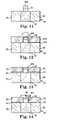
- FIGS. 7–24illustrate two embodiments for fabricating a phase-change memory cell.
- FIGS. 7–14 and FIGS. 15–24illustrate embodiments for fabricating a phase-change memory cell, such as phase-change memory cell 30 illustrated in FIG. 4 .
- FIG. 7illustrates a cross-sectional view through a phase-change memory cell 30 in accordance with another embodiment of the present invention.
- Phase-change memory cell 30includes first electrode 32 , phase-change material 34 , second electrode 36 , and insulator material 38 .
- phase-change memory cell 30includes optional diffusion barrier 42 adjacent phase-change material 34 , and isolation material 40 adjacent optional diffusion barrier 42 . In other embodiments, diffusion barrier 42 is excluded.
- Phase-change material 34provides a storage location for storing a bit of data.
- Diffusion barrier 42prevents the diffusion of phase-change material 34 into isolation material 40 .
- diffusion barrier 42includes SiN or another suitable barrier material.
- isolation material 40is selected to have low thermal conductivity/diffusivity, thereby reducing the heat leakage from the edges of phase-change material 34 .
- phase-change memory cell 30is a pillar AIV phase-change memory cell. The process for fabricating this embodiment of memory cell 30 is illustrated in the following FIGS. 8–14 .
- FIG. 8illustrates a cross-sectional view of one embodiment of a preprocessed wafer 39 .
- Preprocessed wafer 39includes insulation material 38 , first electrode 32 , optional contact material 44 , and lower wafer layers (not shown). In other embodiments, contact material 44 is excluded.
- First electrode 32is a tungsten plug, copper plug, or another suitable electrode.
- Contact material 44comprises Ta, TaN, TiN, or another suitable contact material.
- Optional contact material 44is provided in one embodiment by etching first electrode 32 to form a recess, filling the recess with contact material 44 , and planarizing to provide preprocessed wafer 39 . In other embodiments, contact material 44 is provided using another suitable process.
- FIG. 9illustrates a cross-sectional view of one embodiment of preprocessed wafer 39 , a phase-change material layer 34 a , and an electrode material layer 36 a .
- a planar deposition of phase-change materialsuch as a chalcogenide compound material or another suitable phase-change material, over preprocessed wafer 39 provides phase-change material layer 34 a .
- a planar deposition of electrode material, such as TiN, TaN, or another suitable electrode material, over phase-change material layer 34 aprovides electrode material layer 36 a .
- Phase-change material layer 34 a and electrode material layer 36 aare deposited using chemical vapor deposition (CVD), atomic layer deposition (ALD), metal organic chemical vapor deposition (MOCVD), plasma vapor deposition (PVD), jet vapor deposition (JVP), or other suitable deposition technique.
- CVDchemical vapor deposition
- ALDatomic layer deposition
- MOCVDmetal organic chemical vapor deposition
- PVDplasma vapor deposition
- JVPjet vapor deposition
- FIG. 10illustrates a cross-sectional view of one embodiment of preprocessed wafer 39 , phase-change material layer 34 a , electrode material layer 36 a , and a sublithographic mask layer 46 .
- sublithographic mask layer 46is provided by spin-coating photoresist onto electrode material layer 36 a and performing optical lithography to define an initial mask layer. The initial mask layer is then reduced to provide sublithographic mask layer 46 through a photoresist trimming process. Alternatively, an additional hard mask layer can be used and trimmed using a wet chemical pullback etch.
- sublithographic mask layer 46is positioned approximately above the center of first electrode 32 .
- FIG. 11illustrates a cross-sectional view of one embodiment of preprocessed wafer 39 , phase-change material layer 34 , and electrode material layer 36 b after etching electrode material layer 36 a and phase-change material layer 34 a .
- the portions of electrode material layer 36 a and phase-change material layer 34 a not masked by sublithographic mask layer 46are etched with a dry etch or another suitable etch to provide electrode material layer 36 b and phase-change material layer 34 .
- sublithographic mask layer 46is removed using a photoresist stripping method.
- FIG. 12illustrates a cross-sectional view of one embodiment of preprocessed wafer 39 , phase-change material layer 34 , electrode material layer 36 b , an optional diffusion barrier layer 42 a , and an isolation material layer 40 a .
- optional diffusion barrier layer 42 ais excluded.
- Diffusion barrier layer 42 ais provided by depositing SiN or another suitable barrier material over exposed portions of preprocessed wafer 39 , phase-change material layer 34 , and electrode material layer 36 b using CVD, ALD, MOCVD, PVD, JVP, or other suitable deposition technique. In one embodiment, this deposition is conformal to achieve the same thickness on the sidewalls of phase-change material layer 34 and on exposed portions of preprocessed wafer 39 .
- Isolation material layer 40 ais provided by preferably conformally depositing a material having low thermal conductivity/diffusivity over diffusion barrier material layer 42 a using CVD, ALD, MOCVD, PVD, JVP, or other suitable deposition technique.
- FIG. 13illustrates a cross-sectional view of one embodiment of preprocessed wafer 39 , phase-change material layer 34 , electrode material layer 36 b , diffusion barrier layer 42 , and isolation material layer 40 after planarization of isolation material layer 40 a and diffusion barrier layer 42 a .
- Isolation material layer 40 a and diffusion barrier layer barrier 42 aare planarized to expose electrode material layer 36 b .
- Isolation material layer 40 a and diffusion barrier layer 42 aare planarized using chemical mechanical polishing (CMP) or another suitable planarazation technique to provide isolation material layer 40 and diffusion barrier layer 42 .
- CMPchemical mechanical polishing
- FIG. 14illustrates a cross-sectional view of one embodiment of preprocessed wafer 39 , phase-change material layer 34 , electrode material layer 36 b , diffusion barrier layer 42 , isolation material layer 40 , and an additional electrode material layer after etching the additional electrode material layer.
- an additional diffusion barrier layer(not shown) is deposited over exposed portions of isolation material layer 40 , diffusion barrier layer 42 , and electrode material layer 36 b . The additional diffusion barrier layer is then etched to expose electrode material layer 36 b .
- an additional electrode material layeris deposited over exposed portions of isolation material layer 40 , diffusion barrier layer 42 , and electrode layer 36 b and etched to provide second electrode 36 .
- Second electrode 36comprises TiN, TaN, or another suitable electrode material.
- second electrode 36provides a landing pad for the next level metalization plug. Additional insulation material is then deposited around second electrode 36 to provide phase-change memory cell 30 illustrated in FIG. 7 .
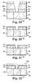
- FIG. 15illustrates a cross-sectional view through a phase-change memory cell 30 in accordance with another embodiment of the present invention.
- Phase-change memory cell 30includes first electrode 32 , phase-change material 34 , second electrode 36 , and insulator material 38 .
- phase-change memory cell 30includes optional diffusion barrier 42 adjacent phase-change material 34 , and isolation material 40 adjacent optional diffusion barrier 42 . In other embodiments, diffusion barrier 42 is excluded.
- Phase-change material 34provides a storage location for storing a bit of data.
- phase-change material 34has vertical sidewalls. In another embodiment, phase-change material 34 has V-shaped sidewalls.
- Diffusion barrier 42prevents the diffusion of phase-change material 34 into isolation material 40 .
- diffusion barrier 42includes SiN or another suitable barrier material.
- isolation material 40is selected to have low thermal conductivity/diffusivity, thereby reducing the heat leakage from the edges of phase-change material 34 .
- phase-change memory cell 30is a V-cell AIV phase-change memory cell. The process for fabricating this embodiment of memory cell 30 is illustrated in the following FIGS. 16–24 .
- FIG. 16illustrates a cross-sectional view of one embodiment of a preprocessed wafer 39 .
- Preprocessed wafer 39includes insulation material 38 , first electrode 32 , optional contact material 44 , and lower wafer layers (not shown). In other embodiments, contact material 44 is excluded.
- First electrode 32is a tungsten plug, copper plug, or another suitable electrode.
- Contact material 44comprises Ta, TaN, TiN, or another suitable contact material.
- Optional contact material 44is provided in one embodiment by etching first electrode 32 to form a recess, filling the recess with contact material 44 , and planarizing to provide preprocessed wafer 39 . In other embodiments, contact material 44 is provided using another suitable process.
- FIG. 17illustrates a cross-sectional view of one embodiment of preprocessed wafer 39 , an isolation material layer 40 a , a stop layer 48 a , and a sacrificial layer 38 a .
- a planar deposition of a material having low thermal conductivity/diffusivity over preprocessed wafer 39provides isolation material layer 40 a .
- a planar deposition of SiN or another suitable material over isolation material layer 40 aprovides stop layer 48 a .
- a planar deposition of an insulating material, such as SiO 2 , over stop layer 48 aprovides sacrificial layer 38 a .
- Isolation material layer 40 , stop layer 48 , and sacrificial layer 38are deposited using CVD, ALD, MOCVD, PVD, JVP, or other suitable deposition technique.
- FIG. 18illustrates a cross-sectional view of one embodiment of preprocessed wafer 39 , isolation material layer 40 a , stop layer 48 a , sacrificial layer 38 b , and a mask layer 46 after etching sacrificial layer 38 a .
- the portion of sacrificial layer 38 a not masked by mask layer 46is etched using a tapered via etch down to stop layer 48 to provide sacrificial layer 38 b .
- the tapered via etchreduces the contact dimensions for phase-change memory cell 30 to sublithographic dimensions.
- the tapered viais positioned approximately above the center of first electrode 32 .
- FIG. 19illustrates a cross-sectional view of one embodiment of preprocessed wafer 39 , isolation material layer 40 , stop layer 48 , sacrificial layer 38 b , and mask layer 46 after etching stop layer 48 a and isolation material layer 40 a .
- Stop layer 48 ais etched using a dry etch or another suitable etch to transfer the sublithographic opening of sacrificial layer 38 b to provide stop layer 48 .
- Isolation material layer 40 ais etched using an oxide etch or another suitable etch to transfer the sublithographic opening of sacrificial layer 38 b to provide isolation material layer 40 having a via positioned approximately above the center of first electrode 32 .
- FIG. 20illustrates a cross-sectional view of one embodiment of preprocessed wafer 39 , isolation material layer 40 , and stop layer 48 after removing mask layer 46 and sacrificial layer 38 b .
- Mask layer 46is removed using an O 2 plasma photoresist strip and dry process or another suitable photoresist removal method.
- Sacrificial layer 38 bis removed using an anisotropic oxide etch or another suitable method.
- FIG. 21illustrates a cross-sectional view of one embodiment of preprocessed wafer 39 , isolation material layer 40 , and an optional diffusion barrier layer 42 after etching the optional diffusion barrier layer.
- diffusion barrier layer 42is excluded.
- Diffusion barrier layer 42is provided by conformally depositing SiN or another suitable barrier material over exposed portions of preprocessed wafer 39 and isolation material layer 40 using CVD, ALD, MOCVD, PVD, JVP, or other suitable deposition technique. An anisotropic back etch or another suitable method is used to remove the diffusion barrier material to expose first electrode 32 .
- both stop layer 48 and diffusion barrier layer 42comprise SiN, therefore stop layer 48 combines with the diffusion barrier layer to provide diffusion barrier layer 42 .
- FIG. 22illustrates a cross-sectional view of one embodiment of preprocessed wafer 39 , isolation material layer 40 , diffusion barrier layer 42 , and a phase-change material layer 34 a .
- Phase-change materialsuch as a chalcogenide compound material or another suitable phase-change material, is deposited over exposed portions of preprocessed wafer 39 and diffusion barrier layer 42 to provide phase-change material layer 34 a .
- Phase-change material layer 34 ais deposited using CVD, ALD, MOCVD, PVD, JVP, or other suitable deposition technique.
- FIG. 23illustrates a cross-sectional view of one embodiment of preprocessed wafer 39 , isolation material layer 40 , diffusion barrier layer 42 , and phase-change material layer 34 after planarization of phase-change material layer 34 a .
- Phase-change material layer 34 ais planarized to expose diffusion barrier layer 42 and provide a sublithographic phase-change material layer 34 .
- Phase-change material layer 34 ais planarized using CMP or another suitable planarization technique.
- FIG. 24illustrates a cross-sectional view of one embodiment of preprocessed wafer 39 , isolation material layer 40 , diffusion barrier layer 42 , phase-change material layer 34 , and second electrode 36 after etching an electrode material layer.
- An electrode material layeris deposited over exposed portions of diffusion barrier layer 42 and phase-change material layer 34 and etched to provide second electrode 36 .
- Second electrode 36comprises TiN, TaN, or another suitable electrode material.
- second electrode 36provides a landing pad for the next level metalization plug. Additional insulation material 38 is then deposited around second electrode 36 to provide phase-change memory cell 30 illustrated in FIG. 15 .
Landscapes
- Engineering & Computer Science (AREA)
- Manufacturing & Machinery (AREA)
- Chemical & Material Sciences (AREA)
- Crystallography & Structural Chemistry (AREA)
- Semiconductor Memories (AREA)
Abstract
Description
Claims (10)
Priority Applications (6)
| Application Number | Priority Date | Filing Date | Title |
|---|---|---|---|
| US11/101,972US7214958B2 (en) | 2005-02-10 | 2005-04-08 | Phase change memory cell with high read margin at low power operation |
| PCT/EP2006/050751WO2006084857A1 (en) | 2005-02-10 | 2006-02-08 | Phase change memory cell with high read margin at low power operation |
| KR1020067014085AKR100873973B1 (en) | 2005-02-10 | 2006-02-08 | Phase Change Memory Cell with High Read Margin with Low Power Operation |
| EP06708098AEP1846962B1 (en) | 2005-02-10 | 2006-02-08 | Phase change memory cell with high read margin at low power operation |
| US11/737,847US7674709B2 (en) | 2005-02-10 | 2007-04-20 | Phase change memory cell with high read margin at low power operation |
| US11/737,838US7714312B2 (en) | 2005-02-10 | 2007-04-20 | Phase change memory cell with high read margin at low power operation |
Applications Claiming Priority (2)
| Application Number | Priority Date | Filing Date | Title |
|---|---|---|---|
| US11/054,853US7361925B2 (en) | 2005-02-10 | 2005-02-10 | Integrated circuit having a memory including a low-k dielectric material for thermal isolation |
| US11/101,972US7214958B2 (en) | 2005-02-10 | 2005-04-08 | Phase change memory cell with high read margin at low power operation |
Related Parent Applications (1)
| Application Number | Title | Priority Date | Filing Date |
|---|---|---|---|
| US11/054,853Continuation-In-PartUS7361925B2 (en) | 2005-02-10 | 2005-02-10 | Integrated circuit having a memory including a low-k dielectric material for thermal isolation |
Related Child Applications (2)
| Application Number | Title | Priority Date | Filing Date |
|---|---|---|---|
| US11/737,847DivisionUS7674709B2 (en) | 2005-02-10 | 2007-04-20 | Phase change memory cell with high read margin at low power operation |
| US11/737,838ContinuationUS7714312B2 (en) | 2005-02-10 | 2007-04-20 | Phase change memory cell with high read margin at low power operation |
Publications (2)
| Publication Number | Publication Date |
|---|---|
| US20060175599A1 US20060175599A1 (en) | 2006-08-10 |
| US7214958B2true US7214958B2 (en) | 2007-05-08 |
Family
ID=36129870
Family Applications (3)
| Application Number | Title | Priority Date | Filing Date |
|---|---|---|---|
| US11/101,972Expired - Fee RelatedUS7214958B2 (en) | 2005-02-10 | 2005-04-08 | Phase change memory cell with high read margin at low power operation |
| US11/737,847Expired - Fee RelatedUS7674709B2 (en) | 2005-02-10 | 2007-04-20 | Phase change memory cell with high read margin at low power operation |
| US11/737,838Expired - Fee RelatedUS7714312B2 (en) | 2005-02-10 | 2007-04-20 | Phase change memory cell with high read margin at low power operation |
Family Applications After (2)
| Application Number | Title | Priority Date | Filing Date |
|---|---|---|---|
| US11/737,847Expired - Fee RelatedUS7674709B2 (en) | 2005-02-10 | 2007-04-20 | Phase change memory cell with high read margin at low power operation |
| US11/737,838Expired - Fee RelatedUS7714312B2 (en) | 2005-02-10 | 2007-04-20 | Phase change memory cell with high read margin at low power operation |
Country Status (4)
| Country | Link |
|---|---|
| US (3) | US7214958B2 (en) |
| EP (1) | EP1846962B1 (en) |
| KR (1) | KR100873973B1 (en) |
| WO (1) | WO2006084857A1 (en) |
Cited By (148)
| Publication number | Priority date | Publication date | Assignee | Title |
|---|---|---|---|---|
| US20060110878A1 (en)* | 2004-11-22 | 2006-05-25 | Macronix International Co., Ltd. | Side wall active pin memory and manufacturing method |
| US20060192193A1 (en)* | 2005-02-25 | 2006-08-31 | Samsung Electronics Co., Ltd. | Phase-change RAM and method for fabricating the same |
| US20060240616A1 (en)* | 2005-04-22 | 2006-10-26 | Micron Technology, Inc. | Memory elements having patterned electrodes and method of forming the same |
| US20060284156A1 (en)* | 2005-06-16 | 2006-12-21 | Thomas Happ | Phase change memory cell defined by imprint lithography |
| US20070108430A1 (en)* | 2005-11-15 | 2007-05-17 | Macronix International Co., Ltd. | Thermally contained/insulated phase change memory device and method (combined) |
| US20070108431A1 (en)* | 2005-11-15 | 2007-05-17 | Chen Shih H | I-shaped phase change memory cell |
| US20070117315A1 (en)* | 2005-11-22 | 2007-05-24 | Macronix International Co., Ltd. | Memory cell device and manufacturing method |
| US20070115794A1 (en)* | 2005-11-21 | 2007-05-24 | Macronix International Co., Ltd. | Thermal isolation for an active-sidewall phase change memory cell |
| US20070121374A1 (en)* | 2005-11-15 | 2007-05-31 | Macronix International Co., Ltd. | Phase Change Memory Device and Manufacturing Method |
| US20070126040A1 (en)* | 2005-11-21 | 2007-06-07 | Hsiang-Lan Lung | Vacuum cell thermal isolation for a phase change memory device |
| US20070128870A1 (en)* | 2005-12-02 | 2007-06-07 | Macronix International Co., Ltd. | Surface Topology Improvement Method for Plug Surface Areas |
| US20070148869A1 (en)* | 2005-12-28 | 2007-06-28 | Dongbu Electronics Co., Ltd. | Method of manufacturing phase-change memory element |
| US20070147105A1 (en)* | 2005-11-28 | 2007-06-28 | Macronix International Co., Ltd. | Phase Change Memory Cell and Manufacturing Method |
| US20070153500A1 (en)* | 2001-11-07 | 2007-07-05 | Michael Waters | Lighting device |
| US20070158690A1 (en)* | 2006-01-09 | 2007-07-12 | Macronix International Co., Ltd. | Programmable Resistive RAM and Manufacturing Method |
| US20070158632A1 (en)* | 2006-01-09 | 2007-07-12 | Macronix International Co., Ltd. | Method for Fabricating a Pillar-Shaped Phase Change Memory Element |
| US20070158862A1 (en)* | 2005-11-21 | 2007-07-12 | Hsiang-Lan Lung | Vacuum jacketed electrode for phase change memory element |
| US20070158633A1 (en)* | 2005-12-27 | 2007-07-12 | Macronix International Co., Ltd. | Method for Forming Self-Aligned Thermal Isolation Cell for a Variable Resistance Memory Array |
| US20070173063A1 (en)* | 2006-01-24 | 2007-07-26 | Macronix International Co., Ltd. | Self-aligned manufacturing method, and manufacturing method for thin film fuse phase change ram |
| US20070190696A1 (en)* | 2005-02-10 | 2007-08-16 | Infineon Technologies Ag | Phase change memory cell with high read margin at low power operation |
| US20070246699A1 (en)* | 2006-04-21 | 2007-10-25 | Hsiang-Lan Lung | Phase change memory cell with vacuum spacer |
| US20070285960A1 (en)* | 2006-05-24 | 2007-12-13 | Macronix International Co., Ltd. | Single-Mask Phase Change Memory Element |
| US20070298535A1 (en)* | 2006-06-27 | 2007-12-27 | Macronix International Co., Ltd. | Memory Cell With Memory Material Insulation and Manufacturing Method |
| US20080064198A1 (en)* | 2006-09-11 | 2008-03-13 | Wolodymyr Czubatyj | Chalcogenide semiconductor memory device with insulating dielectric |
| US20080137400A1 (en)* | 2006-12-06 | 2008-06-12 | Macronix International Co., Ltd. | Phase Change Memory Cell with Thermal Barrier and Method for Fabricating the Same |
| US20080138930A1 (en)* | 2006-12-06 | 2008-06-12 | Macronix International Co., Ltd. | Method for Making a Keyhole Opening during the Manufacture of a Memory Cell |
| US20080142984A1 (en)* | 2006-12-15 | 2008-06-19 | Macronix International Co., Ltd. | Multi-Layer Electrode Structure |
| US20080165571A1 (en)* | 2007-01-09 | 2008-07-10 | Macronix International Co., Ltd. | Method, Apparatus and Computer Program Product for Read Before Programming Process on Multiple Programmable Resistive Memory Cell |
| US20080165572A1 (en)* | 2007-01-09 | 2008-07-10 | Macronix International Co., Ltd. | Method, Apparatus and Computer Program Product for Stepped Reset Programming Process on Programmable Resistive Memory Cell |
| US20080186755A1 (en)* | 2007-02-05 | 2008-08-07 | Macronix International Co., Ltd. | Memory cell device and programming methods |
| US20080191187A1 (en)* | 2007-02-12 | 2008-08-14 | Macronix International Co., Ltd. | Method for manufacturing a phase change memory device with pillar bottom electrode |
| US20080191186A1 (en)* | 2007-02-14 | 2008-08-14 | Macronix International Co., Ltd. | Phase change memory cell with filled sidewall memory element and method for fabricating the same |
| US20080192534A1 (en)* | 2007-02-08 | 2008-08-14 | Macronix International Co., Ltd. | Memory element with reduced-current phase change element |
| US20080266940A1 (en)* | 2005-11-21 | 2008-10-30 | Erh-Kun Lai | Air Cell Thermal Isolation for a Memory Array Formed of a Programmable Resistive Material |
| US20080265234A1 (en)* | 2007-04-30 | 2008-10-30 | Breitwisch Matthew J | Method of Forming Phase Change Memory Cell With Reduced Switchable Volume |
| US7449710B2 (en) | 2005-11-21 | 2008-11-11 | Macronix International Co., Ltd. | Vacuum jacket for phase change memory element |
| US20080283814A1 (en)* | 2007-05-14 | 2008-11-20 | Industrial Technology Research Institute | Phase-change memory element |
| US7459717B2 (en) | 2005-11-28 | 2008-12-02 | Macronix International Co., Ltd. | Phase change memory cell and manufacturing method |
| US20080315174A1 (en)* | 2007-06-20 | 2008-12-25 | Samsung Electronics Co., Ltd. | Variable resistance non-volatile memory cells and methods of fabricating same |
| US20080315359A1 (en)* | 2007-06-21 | 2008-12-25 | Thomas Happ | Integrated circuit including vertical diode |
| US20090003045A1 (en)* | 2007-06-28 | 2009-01-01 | International Business Machines Corporation | Cmos-process-compatible programmable via device |
| US7473576B2 (en) | 2006-12-06 | 2009-01-06 | Macronix International Co., Ltd. | Method for making a self-converged void and bottom electrode for memory cell |
| US7476587B2 (en) | 2006-12-06 | 2009-01-13 | Macronix International Co., Ltd. | Method for making a self-converged memory material element for memory cell |
| US20090014885A1 (en)* | 2007-07-11 | 2009-01-15 | International Business Machines Corporation | Four-Terminal Reconfigurable Devices |
| US7483316B2 (en) | 2007-04-24 | 2009-01-27 | Macronix International Co., Ltd. | Method and apparatus for refreshing programmable resistive memory |
| US7483292B2 (en) | 2007-02-07 | 2009-01-27 | Macronix International Co., Ltd. | Memory cell with separate read and program paths |
| US20090032796A1 (en)* | 2007-07-31 | 2009-02-05 | Macronix International Co., Ltd. | Phase change memory bridge cell |
| US20090033358A1 (en)* | 2007-08-03 | 2009-02-05 | International Business Machines Corporation | Programmable via devices in back end of line level |
| US20090034323A1 (en)* | 2007-08-02 | 2009-02-05 | Macronix International Co., Ltd. | Phase change memory with dual word lines and source lines and method of operating same |
| US20090033360A1 (en)* | 2007-08-03 | 2009-02-05 | International Business Machines Corporation | Programmable via devices with air gap isolation |
| US7504653B2 (en) | 2006-10-04 | 2009-03-17 | Macronix International Co., Ltd. | Memory cell device with circumferentially-extending memory element |
| US20090072215A1 (en)* | 2007-09-14 | 2009-03-19 | Macronix International Co., Ltd. | Phase change memory cell in via array with self-aligned, self-converged bottom electrode and method for manufacturing |
| US20090072216A1 (en)* | 2007-09-14 | 2009-03-19 | Macronix International Co., Ltd. | Phase change memory cell array with self-converged bottom electrode and method for manufacturing |
| US7510929B2 (en) | 2006-10-18 | 2009-03-31 | Macronix International Co., Ltd. | Method for making memory cell device |
| US7514334B2 (en) | 2005-06-17 | 2009-04-07 | Macronix International Co., Ltd. | Thin film plate phase change RAM circuit and manufacturing method |
| US20090095948A1 (en)* | 2007-10-12 | 2009-04-16 | Macronix International Co., Ltd. | Programmable Resistive Memory with Diode Structure |
| US20090122588A1 (en)* | 2007-11-14 | 2009-05-14 | Macronix International Co., Ltd. | Phase change memory cell including a thermal protect bottom electrode and manufacturing methods |
| US7535756B2 (en) | 2007-01-31 | 2009-05-19 | Macronix International Co., Ltd. | Method to tighten set distribution for PCRAM |
| US20090127537A1 (en)* | 2006-03-24 | 2009-05-21 | Nxp B.V. | Electric device with phase change resistor |
| US20090148980A1 (en)* | 2007-12-11 | 2009-06-11 | Industrial Technology Research Institute | Method for forming phase-change memory element |
| US20090147564A1 (en)* | 2007-12-07 | 2009-06-11 | Macronix International Co., Ltd. | Phase change memory cell having interface structures with essentially equal thermal impedances and manufacturing methods |
| US7554144B2 (en) | 2006-04-17 | 2009-06-30 | Macronix International Co., Ltd. | Memory device and manufacturing method |
| US7560337B2 (en) | 2006-01-09 | 2009-07-14 | Macronix International Co., Ltd. | Programmable resistive RAM and manufacturing method |
| US20090184310A1 (en)* | 2008-01-18 | 2009-07-23 | Macronix International Co., Ltd. | Memory cell with memory element contacting an inverted t-shaped bottom electrode |
| US7569844B2 (en) | 2007-04-17 | 2009-08-04 | Macronix International Co., Ltd. | Memory cell sidewall contacting side electrode |
| US20090230378A1 (en)* | 2008-03-11 | 2009-09-17 | Samsung Electronics Co., Ltd. | Resistive memory devices |
| US7619311B2 (en) | 2007-02-02 | 2009-11-17 | Macronix International Co., Ltd. | Memory cell device with coplanar electrode surface and method |
| US7639527B2 (en) | 2008-01-07 | 2009-12-29 | Macronix International Co., Ltd. | Phase change memory dynamic resistance test and manufacturing methods |
| US20090321711A1 (en)* | 2006-10-16 | 2009-12-31 | Takeshi Takagi | Nonvolatile memory element and manufacturing method thereof |
| US20100029062A1 (en)* | 2007-02-21 | 2010-02-04 | Macronix International Co., Ltd. | Programmable resistive memory cell with self-forming gap |
| US7663135B2 (en) | 2007-01-31 | 2010-02-16 | Macronix International Co., Ltd. | Memory cell having a side electrode contact |
| US7696503B2 (en) | 2005-06-17 | 2010-04-13 | Macronix International Co., Ltd. | Multi-level memory cell having phase change element and asymmetrical thermal boundary |
| US7701750B2 (en) | 2008-05-08 | 2010-04-20 | Macronix International Co., Ltd. | Phase change device having two or more substantial amorphous regions in high resistance state |
| US20100117050A1 (en)* | 2008-11-12 | 2010-05-13 | Industrial Technology Research Institute | Phase-change memory element |
| US7719913B2 (en) | 2008-09-12 | 2010-05-18 | Macronix International Co., Ltd. | Sensing circuit for PCRAM applications |
| US7718989B2 (en) | 2006-12-28 | 2010-05-18 | Macronix International Co., Ltd. | Resistor random access memory cell device |
| US7741636B2 (en) | 2006-01-09 | 2010-06-22 | Macronix International Co., Ltd. | Programmable resistive RAM and manufacturing method |
| US7755076B2 (en) | 2007-04-17 | 2010-07-13 | Macronix International Co., Ltd. | 4F2 self align side wall active phase change memory |
| US7772067B2 (en) | 2007-11-19 | 2010-08-10 | Samsung Electronics Co., Ltd. | Methods of forming phase-changeable memory devices using growth-enhancing and growth-inhibiting layers for phase-changeable materials |
| US7772581B2 (en) | 2006-09-11 | 2010-08-10 | Macronix International Co., Ltd. | Memory device having wide area phase change element and small electrode contact area |
| US7777215B2 (en) | 2007-07-20 | 2010-08-17 | Macronix International Co., Ltd. | Resistive memory structure with buffer layer |
| US7786461B2 (en) | 2007-04-03 | 2010-08-31 | Macronix International Co., Ltd. | Memory structure with reduced-size memory element between memory material portions |
| US7785920B2 (en) | 2006-07-12 | 2010-08-31 | Macronix International Co., Ltd. | Method for making a pillar-type phase change memory element |
| US7786460B2 (en) | 2005-11-15 | 2010-08-31 | Macronix International Co., Ltd. | Phase change memory device and manufacturing method |
| US7791057B2 (en) | 2008-04-22 | 2010-09-07 | Macronix International Co., Ltd. | Memory cell having a buried phase change region and method for fabricating the same |
| US7791058B2 (en) | 2006-08-29 | 2010-09-07 | Micron Technology, Inc. | Enhanced memory density resistance variable memory cells, arrays, devices and systems including the same, and methods of fabrication |
| US7825398B2 (en) | 2008-04-07 | 2010-11-02 | Macronix International Co., Ltd. | Memory cell having improved mechanical stability |
| US7863655B2 (en) | 2006-10-24 | 2011-01-04 | Macronix International Co., Ltd. | Phase change memory cells with dual access devices |
| US7867815B2 (en) | 2005-11-16 | 2011-01-11 | Macronix International Co., Ltd. | Spacer electrode small pin phase change RAM and manufacturing method |
| US7869270B2 (en) | 2008-12-29 | 2011-01-11 | Macronix International Co., Ltd. | Set algorithm for phase change memory cell |
| US7879645B2 (en) | 2008-01-28 | 2011-02-01 | Macronix International Co., Ltd. | Fill-in etching free pore device |
| US7894254B2 (en) | 2009-07-15 | 2011-02-22 | Macronix International Co., Ltd. | Refresh circuitry for phase change memory |
| US7897954B2 (en) | 2008-10-10 | 2011-03-01 | Macronix International Co., Ltd. | Dielectric-sandwiched pillar memory device |
| US7903447B2 (en) | 2006-12-13 | 2011-03-08 | Macronix International Co., Ltd. | Method, apparatus and computer program product for read before programming process on programmable resistive memory cell |
| US7903457B2 (en) | 2008-08-19 | 2011-03-08 | Macronix International Co., Ltd. | Multiple phase change materials in an integrated circuit for system on a chip application |
| US7919766B2 (en) | 2007-10-22 | 2011-04-05 | Macronix International Co., Ltd. | Method for making self aligning pillar memory cell device |
| US7933139B2 (en) | 2009-05-15 | 2011-04-26 | Macronix International Co., Ltd. | One-transistor, one-resistor, one-capacitor phase change memory |
| US7932506B2 (en) | 2008-07-22 | 2011-04-26 | Macronix International Co., Ltd. | Fully self-aligned pore-type memory cell having diode access device |
| US7956344B2 (en) | 2007-02-27 | 2011-06-07 | Macronix International Co., Ltd. | Memory cell with memory element contacting ring-shaped upper end of bottom electrode |
| US7956358B2 (en) | 2006-02-07 | 2011-06-07 | Macronix International Co., Ltd. | I-shaped phase change memory cell with thermal isolation |
| US7968927B2 (en) | 2005-04-22 | 2011-06-28 | Micron Technology, Inc. | Memory array for increased bit density and method of forming the same |
| US7968876B2 (en) | 2009-05-22 | 2011-06-28 | Macronix International Co., Ltd. | Phase change memory cell having vertical channel access transistor |
| US20110186800A1 (en)* | 2008-01-29 | 2011-08-04 | International Business Machines Corporation | Pore phase change material cell fabricated from recessed pillar |
| US20110191928A1 (en)* | 2008-02-26 | 2011-08-11 | Ardiff Henry G | Low weight and high durability soft body armor composite using topical wax coatings |
| US8030635B2 (en) | 2009-01-13 | 2011-10-04 | Macronix International Co., Ltd. | Polysilicon plug bipolar transistor for phase change memory |
| US8030634B2 (en) | 2008-03-31 | 2011-10-04 | Macronix International Co., Ltd. | Memory array with diode driver and method for fabricating the same |
| US8036014B2 (en)* | 2008-11-06 | 2011-10-11 | Macronix International Co., Ltd. | Phase change memory program method without over-reset |
| US8062833B2 (en) | 2005-12-30 | 2011-11-22 | Macronix International Co., Ltd. | Chalcogenide layer etching method |
| US8064248B2 (en) | 2009-09-17 | 2011-11-22 | Macronix International Co., Ltd. | 2T2R-1T1R mix mode phase change memory array |
| US8064247B2 (en) | 2009-01-14 | 2011-11-22 | Macronix International Co., Ltd. | Rewritable memory device based on segregation/re-absorption |
| US8077505B2 (en) | 2008-05-07 | 2011-12-13 | Macronix International Co., Ltd. | Bipolar switching of phase change device |
| US8084760B2 (en) | 2009-04-20 | 2011-12-27 | Macronix International Co., Ltd. | Ring-shaped electrode and manufacturing method for same |
| US8084842B2 (en) | 2008-03-25 | 2011-12-27 | Macronix International Co., Ltd. | Thermally stabilized electrode structure |
| US8089137B2 (en) | 2009-01-07 | 2012-01-03 | Macronix International Co., Ltd. | Integrated circuit memory with single crystal silicon on silicide driver and manufacturing method |
| US8097871B2 (en) | 2009-04-30 | 2012-01-17 | Macronix International Co., Ltd. | Low operational current phase change memory structures |
| US8107283B2 (en) | 2009-01-12 | 2012-01-31 | Macronix International Co., Ltd. | Method for setting PCRAM devices |
| US8110822B2 (en) | 2009-07-15 | 2012-02-07 | Macronix International Co., Ltd. | Thermal protect PCRAM structure and methods for making |
| US8134857B2 (en) | 2008-06-27 | 2012-03-13 | Macronix International Co., Ltd. | Methods for high speed reading operation of phase change memory and device employing same |
| US8158965B2 (en) | 2008-02-05 | 2012-04-17 | Macronix International Co., Ltd. | Heating center PCRAM structure and methods for making |
| US8173987B2 (en) | 2009-04-27 | 2012-05-08 | Macronix International Co., Ltd. | Integrated circuit 3D phase change memory array and manufacturing method |
| US8178387B2 (en) | 2009-10-23 | 2012-05-15 | Macronix International Co., Ltd. | Methods for reducing recrystallization time for a phase change material |
| US8198619B2 (en) | 2009-07-15 | 2012-06-12 | Macronix International Co., Ltd. | Phase change memory cell structure |
| US8238149B2 (en) | 2009-06-25 | 2012-08-07 | Macronix International Co., Ltd. | Methods and apparatus for reducing defect bits in phase change memory |
| US8284596B2 (en) | 2008-06-09 | 2012-10-09 | Qimonda Ag | Integrated circuit including an array of diodes coupled to a layer of resistance changing material |
| US8310864B2 (en) | 2010-06-15 | 2012-11-13 | Macronix International Co., Ltd. | Self-aligned bit line under word line memory array |
| US8324605B2 (en) | 2008-10-02 | 2012-12-04 | Macronix International Co., Ltd. | Dielectric mesh isolated phase change structure for phase change memory |
| US8350316B2 (en) | 2009-05-22 | 2013-01-08 | Macronix International Co., Ltd. | Phase change memory cells having vertical channel access transistor and memory plane |
| US8363463B2 (en) | 2009-06-25 | 2013-01-29 | Macronix International Co., Ltd. | Phase change memory having one or more non-constant doping profiles |
| US8395935B2 (en) | 2010-10-06 | 2013-03-12 | Macronix International Co., Ltd. | Cross-point self-aligned reduced cell size phase change memory |
| US8406033B2 (en) | 2009-06-22 | 2013-03-26 | Macronix International Co., Ltd. | Memory device and method for sensing and fixing margin cells |
| US8415651B2 (en) | 2008-06-12 | 2013-04-09 | Macronix International Co., Ltd. | Phase change memory cell having top and bottom sidewall contacts |
| US8426838B2 (en) | 2008-01-25 | 2013-04-23 | Higgs Opl. Capital Llc | Phase-change memory |
| US8467238B2 (en) | 2010-11-15 | 2013-06-18 | Macronix International Co., Ltd. | Dynamic pulse operation for phase change memory |
| US8497705B2 (en) | 2010-11-09 | 2013-07-30 | Macronix International Co., Ltd. | Phase change device for interconnection of programmable logic device |
| US8513637B2 (en) | 2007-07-13 | 2013-08-20 | Macronix International Co., Ltd. | 4F2 self align fin bottom electrodes FET drive phase change memory |
| US8610098B2 (en) | 2007-04-06 | 2013-12-17 | Macronix International Co., Ltd. | Phase change memory bridge cell with diode isolation device |
| US8664689B2 (en) | 2008-11-07 | 2014-03-04 | Macronix International Co., Ltd. | Memory cell access device having a pn-junction with polycrystalline plug and single-crystal semiconductor regions |
| US8729521B2 (en) | 2010-05-12 | 2014-05-20 | Macronix International Co., Ltd. | Self aligned fin-type programmable memory cell |
| US8809829B2 (en) | 2009-06-15 | 2014-08-19 | Macronix International Co., Ltd. | Phase change memory having stabilized microstructure and manufacturing method |
| US8907316B2 (en) | 2008-11-07 | 2014-12-09 | Macronix International Co., Ltd. | Memory cell access device having a pn-junction with polycrystalline and single crystal semiconductor regions |
| US8933536B2 (en) | 2009-01-22 | 2015-01-13 | Macronix International Co., Ltd. | Polysilicon pillar bipolar transistor with self-aligned memory element |
| US8987700B2 (en) | 2011-12-02 | 2015-03-24 | Macronix International Co., Ltd. | Thermally confined electrode for programmable resistance memory |
| US9018615B2 (en) | 2007-08-03 | 2015-04-28 | Macronix International Co., Ltd. | Resistor random access memory structure having a defined small area of electrical contact |
| US9159412B1 (en) | 2014-07-15 | 2015-10-13 | Macronix International Co., Ltd. | Staggered write and verify for phase change memory |
| US9336879B2 (en) | 2014-01-24 | 2016-05-10 | Macronix International Co., Ltd. | Multiple phase change materials in an integrated circuit for system on a chip application |
| US9559113B2 (en) | 2014-05-01 | 2017-01-31 | Macronix International Co., Ltd. | SSL/GSL gate oxide in 3D vertical channel NAND |
| US9672906B2 (en) | 2015-06-19 | 2017-06-06 | Macronix International Co., Ltd. | Phase change memory with inter-granular switching |
| US9997703B2 (en)* | 2013-07-25 | 2018-06-12 | Hewlett Packard Enterprise Development Lp | Resistive memory device having field enhanced features |
Families Citing this family (45)
| Publication number | Priority date | Publication date | Assignee | Title |
|---|---|---|---|---|
| KR100669851B1 (en)* | 2005-07-12 | 2007-01-16 | 삼성전자주식회사 | Manufacturing Method of Phase Change Memory Device |
| JP2007073779A (en)* | 2005-09-07 | 2007-03-22 | Elpida Memory Inc | Nonvolatile memory element and its manufacturing method |
| US7417245B2 (en)* | 2005-11-02 | 2008-08-26 | Infineon Technologies Ag | Phase change memory having multilayer thermal insulation |
| US7910907B2 (en)* | 2006-03-15 | 2011-03-22 | Macronix International Co., Ltd. | Manufacturing method for pipe-shaped electrode phase change memory |
| US7812334B2 (en)* | 2006-04-04 | 2010-10-12 | Micron Technology, Inc. | Phase change memory elements using self-aligned phase change material layers and methods of making and using same |
| US9178141B2 (en) | 2006-04-04 | 2015-11-03 | Micron Technology, Inc. | Memory elements using self-aligned phase change material layers and methods of manufacturing same |
| KR100791477B1 (en)* | 2006-08-08 | 2008-01-03 | 삼성전자주식회사 | Phase change memory unit, manufacturing method thereof, phase change memory device including same and manufacturing method thereof |
| US7638357B2 (en)* | 2006-08-25 | 2009-12-29 | Micron Technology, Inc. | Programmable resistance memory devices and systems using the same and methods of forming the same |
| US7511984B2 (en)* | 2006-08-30 | 2009-03-31 | Micron Technology, Inc. | Phase change memory |
| US8017930B2 (en)* | 2006-12-21 | 2011-09-13 | Qimonda Ag | Pillar phase change memory cell |
| US20080164453A1 (en)* | 2007-01-07 | 2008-07-10 | Breitwisch Matthew J | Uniform critical dimension size pore for pcram application |
| KR100801084B1 (en) | 2007-01-08 | 2008-02-05 | 삼성전자주식회사 | Nonvolatile Memory Device Using Resistor and Manufacturing Method Thereof |
| KR100883412B1 (en)* | 2007-05-09 | 2009-02-11 | 삼성전자주식회사 | Method for manufacturing phase change memory device having self-aligned electrode, related device and electronic system |
| US20080278988A1 (en)* | 2007-05-09 | 2008-11-13 | Klaus Ufert | Resistive switching element |
| DE102007021761B4 (en)* | 2007-05-09 | 2015-07-16 | Adesto Technology Corp., Inc. | Resistor switching element, memory devices, memory module, method for producing a resistive switching element and method for producing a resistive memory device |
| US7678642B2 (en)* | 2007-05-11 | 2010-03-16 | Hynix Semiconductor Inc. | Method for manufacturing phase change memory device using a patterning process |
| US7671353B2 (en)* | 2007-06-04 | 2010-03-02 | Qimonda North America Corp. | Integrated circuit having contact including material between sidewalls |
| US8410607B2 (en)* | 2007-06-15 | 2013-04-02 | Taiwan Semiconductor Manufacturing Co., Ltd. | Semiconductor memory structures |
| US8076664B2 (en)* | 2007-12-20 | 2011-12-13 | Intel Corporation | Phase change memory with layered insulator |
| US7906774B2 (en)* | 2008-02-01 | 2011-03-15 | Industrial Technology Research Institute | Phase change memory device |
| US7935564B2 (en) | 2008-02-25 | 2011-05-03 | International Business Machines Corporation | Self-converging bottom electrode ring |
| KR100979755B1 (en)* | 2008-03-28 | 2010-09-02 | 삼성전자주식회사 | Phase change memory device and manufacturing methods thereof |
| KR20110110187A (en)* | 2008-12-18 | 2011-10-06 | 비코 인스트루먼트 아이엔씨. | Vacuum Evaporation Source with Thermal Diffusion Orifice |
| US7888155B2 (en)* | 2009-03-16 | 2011-02-15 | Industrial Technology Research Institute | Phase-change memory element and method for fabricating the same |
| US8012790B2 (en)* | 2009-08-28 | 2011-09-06 | International Business Machines Corporation | Chemical mechanical polishing stop layer for fully amorphous phase change memory pore cell |
| US8283650B2 (en) | 2009-08-28 | 2012-10-09 | International Business Machines Corporation | Flat lower bottom electrode for phase change memory cell |
| US8283202B2 (en) | 2009-08-28 | 2012-10-09 | International Business Machines Corporation | Single mask adder phase change memory element |
| US20110057161A1 (en)* | 2009-09-10 | 2011-03-10 | Gurtej Sandhu | Thermally shielded resistive memory element for low programming current |
| JP2011066135A (en)* | 2009-09-16 | 2011-03-31 | Elpida Memory Inc | Method for fabricating phase-change memory device |
| US8129268B2 (en) | 2009-11-16 | 2012-03-06 | International Business Machines Corporation | Self-aligned lower bottom electrode |
| US7943420B1 (en) | 2009-11-25 | 2011-05-17 | International Business Machines Corporation | Single mask adder phase change memory element |
| CN102648522B (en)* | 2009-11-30 | 2014-10-22 | 松下电器产业株式会社 | Nonvolatile storage element, manufacturing method thereof, and nonvolatile storage device |
| CN102237492B (en)* | 2010-04-29 | 2013-04-17 | 中芯国际集成电路制造(上海)有限公司 | Formation method for phase-change memory unit |
| US8395137B2 (en)* | 2011-03-08 | 2013-03-12 | Micron Technology, Inc. | Memory cell constructions |
| CN103840077B (en)* | 2012-11-27 | 2016-04-20 | 中芯国际集成电路制造(上海)有限公司 | The manufacture method of phase transition storage |
| US9012880B2 (en)* | 2013-02-21 | 2015-04-21 | Winbond Electronics Corp. | Resistance memory device |
| CN106654004B (en)* | 2015-10-29 | 2019-03-19 | 华邦电子股份有限公司 | Resistive memory and manufacturing method thereof |
| GB201717566D0 (en)* | 2017-10-25 | 2017-12-06 | Bodle Tech Ltd | Display apparatus |
| US10490744B2 (en)* | 2017-11-07 | 2019-11-26 | Macronix International Co., Ltd. | Contact hole structure method for fabricating the same and applications thereof |
| TWI702744B (en)* | 2018-04-30 | 2020-08-21 | 華邦電子股份有限公司 | Resistive random access memory structure and manufacturing method thereof |
| CN110473961B (en)* | 2018-05-10 | 2023-04-14 | 华邦电子股份有限公司 | Resistive random access memory structure and manufacturing method thereof |
| KR20200022945A (en)* | 2018-08-24 | 2020-03-04 | 삼성전자주식회사 | Variable resistance memory device |
| CN111540828A (en)* | 2020-03-23 | 2020-08-14 | 江苏时代全芯存储科技股份有限公司 | Forming method of phase change memory |
| CN112909161B (en)* | 2021-01-05 | 2022-03-11 | 华中科技大学 | Low-power-consumption phase change memory unit with buffer layer and preparation method thereof |
| US20240130252A1 (en)* | 2022-10-17 | 2024-04-18 | Taiwan Semiconductor Manufacturing Company, Ltd. | Thermal barrier structure in phase change material device |
Citations (14)
| Publication number | Priority date | Publication date | Assignee | Title |
|---|---|---|---|---|
| US5751012A (en) | 1995-06-07 | 1998-05-12 | Micron Technology, Inc. | Polysilicon pillar diode for use in a non-volatile memory cell |
| US5837564A (en) | 1995-11-01 | 1998-11-17 | Micron Technology, Inc. | Method for optimal crystallization to obtain high electrical performance from chalcogenides |
| US20010002046A1 (en)* | 1997-05-09 | 2001-05-31 | Reinberg Alan R. | Small electrode for a chalcogenide switching device and method for fabricating same |
| US20020017701A1 (en) | 1999-03-25 | 2002-02-14 | Patrick Klersy | Electrically programmable memory element with raised pore |
| US20030003647A1 (en) | 2001-06-30 | 2003-01-02 | Dennison Charles H. | Reduced area intersection between electrode and programming element |
| EP1318552A1 (en) | 2001-12-05 | 2003-06-11 | STMicroelectronics S.r.l. | Small area contact region, high efficiency phase change memory cell and fabrication method thereof |
| US20030156468A1 (en)* | 2002-02-20 | 2003-08-21 | Campbell Kristy A. | Resistance variable 'on' memory |
| US6625054B2 (en) | 2001-12-28 | 2003-09-23 | Intel Corporation | Method and apparatus to program a phase change memory |
| US20030194865A1 (en) | 2002-04-10 | 2003-10-16 | Gilton Terry L. | Method of manufacture of programmable conductor memory |
| US6673648B2 (en) | 2001-11-08 | 2004-01-06 | Intel Corporation | Isolating phase change material memory cells |
| DE10236439B3 (en) | 2002-08-08 | 2004-02-26 | Infineon Technologies Ag | Memory arrangement comprises a substrate, memory regions formed in and/or on the substrate with electrical resistances that can be adjusted by thermal treatment and structure arranged between the memory regions to remove heat |
| DE10231646A1 (en) | 2002-07-12 | 2004-04-08 | Infineon Technologies Ag | Memory cell for permanently storing data has a switching unit with a field effect transistor having a drain region formed as the heating region |
| US6791107B2 (en) | 2000-12-27 | 2004-09-14 | Ovonyx, Inc. | Silicon on insulator phase change memory |
| US20040251551A1 (en) | 2003-06-11 | 2004-12-16 | Horii Hideki | Phase changeable memory devices including carbon nano tubes and methods for forming the same |
Family Cites Families (14)
| Publication number | Priority date | Publication date | Assignee | Title |
|---|---|---|---|---|
| US5325913A (en)* | 1993-06-25 | 1994-07-05 | The United States Of America As Represented By The Secretary Of The Navy | Module cooling system |
| US6087674A (en)* | 1996-10-28 | 2000-07-11 | Energy Conversion Devices, Inc. | Memory element with memory material comprising phase-change material and dielectric material |
| US5825046A (en)* | 1996-10-28 | 1998-10-20 | Energy Conversion Devices, Inc. | Composite memory material comprising a mixture of phase-change memory material and dielectric material |
| US6511867B2 (en)* | 2001-06-30 | 2003-01-28 | Ovonyx, Inc. | Utilizing atomic layer deposition for programmable device |
| US6511862B2 (en)* | 2001-06-30 | 2003-01-28 | Ovonyx, Inc. | Modified contact for programmable devices |
| US6764894B2 (en)* | 2001-08-31 | 2004-07-20 | Ovonyx, Inc. | Elevated pore phase-change memory |
| US6507061B1 (en) | 2001-08-31 | 2003-01-14 | Intel Corporation | Multiple layer phase-change memory |
| WO2003085740A1 (en)* | 2002-04-09 | 2003-10-16 | Matsushita Electric Industrial Co., Ltd. | Non-volatile memory and manufacturing method thereof |
| US6864503B2 (en)* | 2002-08-09 | 2005-03-08 | Macronix International Co., Ltd. | Spacer chalcogenide memory method and device |
| KR100543445B1 (en)* | 2003-03-04 | 2006-01-23 | 삼성전자주식회사 | Phase change memory device and its formation method |
| US20050018526A1 (en)* | 2003-07-21 | 2005-01-27 | Heon Lee | Phase-change memory device and manufacturing method thereof |
| AU2005204368A1 (en)* | 2004-01-06 | 2005-07-28 | Aspen Aerogels, Inc. | Ormosil aerogels containing silicon bonded linear polymers |
| US7214958B2 (en)* | 2005-02-10 | 2007-05-08 | Infineon Technologies Ag | Phase change memory cell with high read margin at low power operation |
| JP2006352082A (en)* | 2005-05-19 | 2006-12-28 | Renesas Technology Corp | Semiconductor memory device and manufacturing method thereof |
- 2005
- 2005-04-08USUS11/101,972patent/US7214958B2/ennot_activeExpired - Fee Related
- 2006
- 2006-02-08EPEP06708098Apatent/EP1846962B1/ennot_activeExpired - Fee Related
- 2006-02-08KRKR1020067014085Apatent/KR100873973B1/ennot_activeExpired - Fee Related
- 2006-02-08WOPCT/EP2006/050751patent/WO2006084857A1/enactiveApplication Filing
- 2007
- 2007-04-20USUS11/737,847patent/US7674709B2/ennot_activeExpired - Fee Related
- 2007-04-20USUS11/737,838patent/US7714312B2/ennot_activeExpired - Fee Related
Patent Citations (14)
| Publication number | Priority date | Publication date | Assignee | Title |
|---|---|---|---|---|
| US5751012A (en) | 1995-06-07 | 1998-05-12 | Micron Technology, Inc. | Polysilicon pillar diode for use in a non-volatile memory cell |
| US5837564A (en) | 1995-11-01 | 1998-11-17 | Micron Technology, Inc. | Method for optimal crystallization to obtain high electrical performance from chalcogenides |
| US20010002046A1 (en)* | 1997-05-09 | 2001-05-31 | Reinberg Alan R. | Small electrode for a chalcogenide switching device and method for fabricating same |
| US20020017701A1 (en) | 1999-03-25 | 2002-02-14 | Patrick Klersy | Electrically programmable memory element with raised pore |
| US6791107B2 (en) | 2000-12-27 | 2004-09-14 | Ovonyx, Inc. | Silicon on insulator phase change memory |
| US20030003647A1 (en) | 2001-06-30 | 2003-01-02 | Dennison Charles H. | Reduced area intersection between electrode and programming element |
| US6673648B2 (en) | 2001-11-08 | 2004-01-06 | Intel Corporation | Isolating phase change material memory cells |
| EP1318552A1 (en) | 2001-12-05 | 2003-06-11 | STMicroelectronics S.r.l. | Small area contact region, high efficiency phase change memory cell and fabrication method thereof |
| US6625054B2 (en) | 2001-12-28 | 2003-09-23 | Intel Corporation | Method and apparatus to program a phase change memory |
| US20030156468A1 (en)* | 2002-02-20 | 2003-08-21 | Campbell Kristy A. | Resistance variable 'on' memory |
| US20030194865A1 (en) | 2002-04-10 | 2003-10-16 | Gilton Terry L. | Method of manufacture of programmable conductor memory |
| DE10231646A1 (en) | 2002-07-12 | 2004-04-08 | Infineon Technologies Ag | Memory cell for permanently storing data has a switching unit with a field effect transistor having a drain region formed as the heating region |
| DE10236439B3 (en) | 2002-08-08 | 2004-02-26 | Infineon Technologies Ag | Memory arrangement comprises a substrate, memory regions formed in and/or on the substrate with electrical resistances that can be adjusted by thermal treatment and structure arranged between the memory regions to remove heat |
| US20040251551A1 (en) | 2003-06-11 | 2004-12-16 | Horii Hideki | Phase changeable memory devices including carbon nano tubes and methods for forming the same |
Non-Patent Citations (6)
| Title |
|---|
| CW Jeong et al., "Switching Current Scaling and Reliability Evaluation on PRAM", IEEE NVSMW, 2004 (pp. 28-29). |
| EU research project ULISSE, final report, 2003; http://www.leti.cea.fr/commun/europe/ulisse/ulisse.htm. |
| H.Horii et al., "A novel cell technology using N-doped GeSbTe films for phase change RAM", VLSI, 2003 (pp. 177-178). |
| S. Lai et al., OUM-a 180 nm nonvolatile memory cell element technology for stand alone and embedded applications, IEDM 2001 (6 pgs.). |
| Y. H Ha, et al., "An edge contact type cell for phase change RAM featuring very low power consumption", VLSI, 2003 (2 pgs.). |
| Y.N. Hwang et al., "Full integration and reliability evaluation of phase-change RAM based on 0.24 mum-CMOS technologies", VLSI 2003 (pp. 173-174). |
Cited By (272)
| Publication number | Priority date | Publication date | Assignee | Title |
|---|---|---|---|---|
| US20070153500A1 (en)* | 2001-11-07 | 2007-07-05 | Michael Waters | Lighting device |
| US7608503B2 (en) | 2004-11-22 | 2009-10-27 | Macronix International Co., Ltd. | Side wall active pin memory and manufacturing method |
| US20060110878A1 (en)* | 2004-11-22 | 2006-05-25 | Macronix International Co., Ltd. | Side wall active pin memory and manufacturing method |
| US20070190696A1 (en)* | 2005-02-10 | 2007-08-16 | Infineon Technologies Ag | Phase change memory cell with high read margin at low power operation |
| US20070187664A1 (en)* | 2005-02-10 | 2007-08-16 | Infineon Technologies Ag | Phase change memory cell with high read margin at low power operation |
| US7674709B2 (en) | 2005-02-10 | 2010-03-09 | Qimonda Ag | Phase change memory cell with high read margin at low power operation |
| US7714312B2 (en)* | 2005-02-10 | 2010-05-11 | Qimonda Ag | Phase change memory cell with high read margin at low power operation |
| US7541633B2 (en)* | 2005-02-25 | 2009-06-02 | Samsung Electronics Co., Ltd. | Phase-change RAM and method for fabricating the same |
| US7872250B2 (en) | 2005-02-25 | 2011-01-18 | Samsung Electronics Co., Ltd. | Phase-change ram and method for fabricating the same |
| US20090236582A1 (en)* | 2005-02-25 | 2009-09-24 | Samsung Electronics Co., Ltd. | Phase-change ram and method for fabricating the same |
| US20060192193A1 (en)* | 2005-02-25 | 2006-08-31 | Samsung Electronics Co., Ltd. | Phase-change RAM and method for fabricating the same |
| US7709289B2 (en)* | 2005-04-22 | 2010-05-04 | Micron Technology, Inc. | Memory elements having patterned electrodes and method of forming the same |
| US7968927B2 (en) | 2005-04-22 | 2011-06-28 | Micron Technology, Inc. | Memory array for increased bit density and method of forming the same |
| US20060240616A1 (en)* | 2005-04-22 | 2006-10-26 | Micron Technology, Inc. | Memory elements having patterned electrodes and method of forming the same |
| US20060284156A1 (en)* | 2005-06-16 | 2006-12-21 | Thomas Happ | Phase change memory cell defined by imprint lithography |
| US7964468B2 (en) | 2005-06-17 | 2011-06-21 | Macronix International Co., Ltd. | Multi-level memory cell having phase change element and asymmetrical thermal boundary |
| US7696503B2 (en) | 2005-06-17 | 2010-04-13 | Macronix International Co., Ltd. | Multi-level memory cell having phase change element and asymmetrical thermal boundary |
| US7514334B2 (en) | 2005-06-17 | 2009-04-07 | Macronix International Co., Ltd. | Thin film plate phase change RAM circuit and manufacturing method |
| US20080166875A1 (en)* | 2005-11-15 | 2008-07-10 | Macronix International Co., Ltd. | Thermally contained/insulated phase change memory device and method (combined) |
| US7394088B2 (en)* | 2005-11-15 | 2008-07-01 | Macronix International Co., Ltd. | Thermally contained/insulated phase change memory device and method (combined) |
| US7471555B2 (en) | 2005-11-15 | 2008-12-30 | Macronix International Co., Ltd. | Thermally insulated phase change memory device |
| US7642123B2 (en) | 2005-11-15 | 2010-01-05 | Macronix International Co., Ltd. | Thermally insulated phase change memory manufacturing method |
| US8008114B2 (en) | 2005-11-15 | 2011-08-30 | Macronix International Co., Ltd. | Phase change memory device and manufacturing method |
| US7450411B2 (en) | 2005-11-15 | 2008-11-11 | Macronix International Co., Ltd. | Phase change memory device and manufacturing method |
| US20080268565A1 (en)* | 2005-11-15 | 2008-10-30 | Macronix International Co., Ltd. | Thermally insulated phase change memory manufacturing method |
| US20070108430A1 (en)* | 2005-11-15 | 2007-05-17 | Macronix International Co., Ltd. | Thermally contained/insulated phase change memory device and method (combined) |
| US7635855B2 (en) | 2005-11-15 | 2009-12-22 | Macronix International Co., Ltd. | I-shaped phase change memory cell |
| US7932101B2 (en) | 2005-11-15 | 2011-04-26 | Macronix International Co., Ltd. | Thermally contained/insulated phase change memory device and method |
| US7993962B2 (en) | 2005-11-15 | 2011-08-09 | Macronix International Co., Ltd. | I-shaped phase change memory cell |
| US20070121374A1 (en)* | 2005-11-15 | 2007-05-31 | Macronix International Co., Ltd. | Phase Change Memory Device and Manufacturing Method |
| US7786460B2 (en) | 2005-11-15 | 2010-08-31 | Macronix International Co., Ltd. | Phase change memory device and manufacturing method |
| US20070108431A1 (en)* | 2005-11-15 | 2007-05-17 | Chen Shih H | I-shaped phase change memory cell |
| US7867815B2 (en) | 2005-11-16 | 2011-01-11 | Macronix International Co., Ltd. | Spacer electrode small pin phase change RAM and manufacturing method |
| US8110430B2 (en) | 2005-11-21 | 2012-02-07 | Macronix International Co., Ltd. | Vacuum jacket for phase change memory element |
| US20080266940A1 (en)* | 2005-11-21 | 2008-10-30 | Erh-Kun Lai | Air Cell Thermal Isolation for a Memory Array Formed of a Programmable Resistive Material |
| US7829876B2 (en) | 2005-11-21 | 2010-11-09 | Macronix International Co., Ltd. | Vacuum cell thermal isolation for a phase change memory device |
| US7842536B2 (en) | 2005-11-21 | 2010-11-30 | Macronix International Co., Ltd. | Vacuum jacket for phase change memory element |
| US20070126040A1 (en)* | 2005-11-21 | 2007-06-07 | Hsiang-Lan Lung | Vacuum cell thermal isolation for a phase change memory device |
| US7816661B2 (en) | 2005-11-21 | 2010-10-19 | Macronix International Co., Ltd. | Air cell thermal isolation for a memory array formed of a programmable resistive material |
| US20090098678A1 (en)* | 2005-11-21 | 2009-04-16 | Macronix International Co., Ltd. | Vacuum jacketed electrode for phase change memory element |
| US7479649B2 (en) | 2005-11-21 | 2009-01-20 | Macronix International Co., Ltd. | Vacuum jacketed electrode for phase change memory element |
| US8097487B2 (en) | 2005-11-21 | 2012-01-17 | Macronix International Co., Ltd. | Method for making a phase change memory device with vacuum cell thermal isolation |
| US7687307B2 (en) | 2005-11-21 | 2010-03-30 | Macronix International Co., Ltd. | Vacuum jacketed electrode for phase change memory element |
| US7507986B2 (en) | 2005-11-21 | 2009-03-24 | Macronix International Co., Ltd. | Thermal isolation for an active-sidewall phase change memory cell |
| US7449710B2 (en) | 2005-11-21 | 2008-11-11 | Macronix International Co., Ltd. | Vacuum jacket for phase change memory element |
| US20070115794A1 (en)* | 2005-11-21 | 2007-05-24 | Macronix International Co., Ltd. | Thermal isolation for an active-sidewall phase change memory cell |
| US20070158862A1 (en)* | 2005-11-21 | 2007-07-12 | Hsiang-Lan Lung | Vacuum jacketed electrode for phase change memory element |
| US20070117315A1 (en)* | 2005-11-22 | 2007-05-24 | Macronix International Co., Ltd. | Memory cell device and manufacturing method |
| US7599217B2 (en)* | 2005-11-22 | 2009-10-06 | Macronix International Co., Ltd. | Memory cell device and manufacturing method |
| US7902538B2 (en) | 2005-11-28 | 2011-03-08 | Macronix International Co., Ltd. | Phase change memory cell with first and second transition temperature portions |
| US7929340B2 (en) | 2005-11-28 | 2011-04-19 | Macronix International Co., Ltd. | Phase change memory cell and manufacturing method |
| US7459717B2 (en) | 2005-11-28 | 2008-12-02 | Macronix International Co., Ltd. | Phase change memory cell and manufacturing method |
| US20070147105A1 (en)* | 2005-11-28 | 2007-06-28 | Macronix International Co., Ltd. | Phase Change Memory Cell and Manufacturing Method |
| US7688619B2 (en) | 2005-11-28 | 2010-03-30 | Macronix International Co., Ltd. | Phase change memory cell and manufacturing method |
| US7521364B2 (en) | 2005-12-02 | 2009-04-21 | Macronix Internation Co., Ltd. | Surface topology improvement method for plug surface areas |
| US20070128870A1 (en)* | 2005-12-02 | 2007-06-07 | Macronix International Co., Ltd. | Surface Topology Improvement Method for Plug Surface Areas |
| US7923285B2 (en) | 2005-12-27 | 2011-04-12 | Macronix International, Co. Ltd. | Method for forming self-aligned thermal isolation cell for a variable resistance memory array |
| US7531825B2 (en) | 2005-12-27 | 2009-05-12 | Macronix International Co., Ltd. | Method for forming self-aligned thermal isolation cell for a variable resistance memory array |
| US20070158633A1 (en)* | 2005-12-27 | 2007-07-12 | Macronix International Co., Ltd. | Method for Forming Self-Aligned Thermal Isolation Cell for a Variable Resistance Memory Array |
| US7838413B2 (en)* | 2005-12-28 | 2010-11-23 | Dongbu Electronics Co., Ltd. | Method of manufacturing phase-change memory element |
| US20070148869A1 (en)* | 2005-12-28 | 2007-06-28 | Dongbu Electronics Co., Ltd. | Method of manufacturing phase-change memory element |
| US8062833B2 (en) | 2005-12-30 | 2011-11-22 | Macronix International Co., Ltd. | Chalcogenide layer etching method |
| US7741636B2 (en) | 2006-01-09 | 2010-06-22 | Macronix International Co., Ltd. | Programmable resistive RAM and manufacturing method |
| US8158963B2 (en) | 2006-01-09 | 2012-04-17 | Macronix International Co., Ltd. | Programmable resistive RAM and manufacturing method |
| US7595218B2 (en) | 2006-01-09 | 2009-09-29 | Macronix International Co., Ltd. | Programmable resistive RAM and manufacturing method |
| US20090236743A1 (en)* | 2006-01-09 | 2009-09-24 | Macronix International Co., Ltd. | Programmable Resistive RAM and Manufacturing Method |
| US20070158690A1 (en)* | 2006-01-09 | 2007-07-12 | Macronix International Co., Ltd. | Programmable Resistive RAM and Manufacturing Method |
| US20070158632A1 (en)* | 2006-01-09 | 2007-07-12 | Macronix International Co., Ltd. | Method for Fabricating a Pillar-Shaped Phase Change Memory Element |
| US7560337B2 (en) | 2006-01-09 | 2009-07-14 | Macronix International Co., Ltd. | Programmable resistive RAM and manufacturing method |
| US8178388B2 (en) | 2006-01-09 | 2012-05-15 | Macronix International Co., Ltd. | Programmable resistive RAM and manufacturing method |
| US7432206B2 (en) | 2006-01-24 | 2008-10-07 | Macronix International Co., Ltd. | Self-aligned manufacturing method, and manufacturing method for thin film fuse phase change ram |
| US20070173063A1 (en)* | 2006-01-24 | 2007-07-26 | Macronix International Co., Ltd. | Self-aligned manufacturing method, and manufacturing method for thin film fuse phase change ram |
| US7956358B2 (en) | 2006-02-07 | 2011-06-07 | Macronix International Co., Ltd. | I-shaped phase change memory cell with thermal isolation |
| US7791059B2 (en)* | 2006-03-24 | 2010-09-07 | Nxp B.V. | Electric device with phase change resistor |
| US20090127537A1 (en)* | 2006-03-24 | 2009-05-21 | Nxp B.V. | Electric device with phase change resistor |
| US7554144B2 (en) | 2006-04-17 | 2009-06-30 | Macronix International Co., Ltd. | Memory device and manufacturing method |
| US7972893B2 (en) | 2006-04-17 | 2011-07-05 | Macronix International Co., Ltd. | Memory device manufacturing method |
| US7928421B2 (en) | 2006-04-21 | 2011-04-19 | Macronix International Co., Ltd. | Phase change memory cell with vacuum spacer |
| US20070246699A1 (en)* | 2006-04-21 | 2007-10-25 | Hsiang-Lan Lung | Phase change memory cell with vacuum spacer |
| US20070285960A1 (en)* | 2006-05-24 | 2007-12-13 | Macronix International Co., Ltd. | Single-Mask Phase Change Memory Element |
| US7423300B2 (en) | 2006-05-24 | 2008-09-09 | Macronix International Co., Ltd. | Single-mask phase change memory element |
| US20070298535A1 (en)* | 2006-06-27 | 2007-12-27 | Macronix International Co., Ltd. | Memory Cell With Memory Material Insulation and Manufacturing Method |
| US7696506B2 (en) | 2006-06-27 | 2010-04-13 | Macronix International Co., Ltd. | Memory cell with memory material insulation and manufacturing method |
| US7785920B2 (en) | 2006-07-12 | 2010-08-31 | Macronix International Co., Ltd. | Method for making a pillar-type phase change memory element |
| US8030636B2 (en) | 2006-08-29 | 2011-10-04 | Micron Technology, Inc. | Enhanced memory density resistance variable memory cells, arrays, devices and systems including the same, and methods of fabrication |
| US20100295011A1 (en)* | 2006-08-29 | 2010-11-25 | Jun Liu | Enhanced memory density resistance variable memory cells, arrays, devices and systems including the same, and methods of fabrication |
| US7791058B2 (en) | 2006-08-29 | 2010-09-07 | Micron Technology, Inc. | Enhanced memory density resistance variable memory cells, arrays, devices and systems including the same, and methods of fabrication |
| US20100261329A1 (en)* | 2006-09-11 | 2010-10-14 | Macronix International Co., Ltd. | Memory device having wide area phase change element and small electrode contact area |
| US20080064198A1 (en)* | 2006-09-11 | 2008-03-13 | Wolodymyr Czubatyj | Chalcogenide semiconductor memory device with insulating dielectric |
| US7772581B2 (en) | 2006-09-11 | 2010-08-10 | Macronix International Co., Ltd. | Memory device having wide area phase change element and small electrode contact area |
| US7964437B2 (en) | 2006-09-11 | 2011-06-21 | Macronix International Co., Ltd. | Memory device having wide area phase change element and small electrode contact area |
| US7504653B2 (en) | 2006-10-04 | 2009-03-17 | Macronix International Co., Ltd. | Memory cell device with circumferentially-extending memory element |
| US7910906B2 (en) | 2006-10-04 | 2011-03-22 | Macronix International Co., Ltd. | Memory cell device with circumferentially-extending memory element |
| US8796660B2 (en)* | 2006-10-16 | 2014-08-05 | Panasonic Corporation | Nonvolatile memory element comprising a resistance variable element and a diode |
| US20090321711A1 (en)* | 2006-10-16 | 2009-12-31 | Takeshi Takagi | Nonvolatile memory element and manufacturing method thereof |
| US7510929B2 (en) | 2006-10-18 | 2009-03-31 | Macronix International Co., Ltd. | Method for making memory cell device |
| US7863655B2 (en) | 2006-10-24 | 2011-01-04 | Macronix International Co., Ltd. | Phase change memory cells with dual access devices |
| US8110456B2 (en) | 2006-10-24 | 2012-02-07 | Macronix International Co., Ltd. | Method for making a self aligning memory device |
| US7476587B2 (en) | 2006-12-06 | 2009-01-13 | Macronix International Co., Ltd. | Method for making a self-converged memory material element for memory cell |
| US7473576B2 (en) | 2006-12-06 | 2009-01-06 | Macronix International Co., Ltd. | Method for making a self-converged void and bottom electrode for memory cell |
| US7749854B2 (en) | 2006-12-06 | 2010-07-06 | Macronix International Co., Ltd. | Method for making a self-converged memory material element for memory cell |
| US7638359B2 (en) | 2006-12-06 | 2009-12-29 | Macronix International Co., Ltd. | Method for making a self-converged void and bottom electrode for memory cell |
| US20080138930A1 (en)* | 2006-12-06 | 2008-06-12 | Macronix International Co., Ltd. | Method for Making a Keyhole Opening during the Manufacture of a Memory Cell |
| US7682868B2 (en) | 2006-12-06 | 2010-03-23 | Macronix International Co., Ltd. | Method for making a keyhole opening during the manufacture of a memory cell |
| US20080137400A1 (en)* | 2006-12-06 | 2008-06-12 | Macronix International Co., Ltd. | Phase Change Memory Cell with Thermal Barrier and Method for Fabricating the Same |
| US7903447B2 (en) | 2006-12-13 | 2011-03-08 | Macronix International Co., Ltd. | Method, apparatus and computer program product for read before programming process on programmable resistive memory cell |
| US20080142984A1 (en)* | 2006-12-15 | 2008-06-19 | Macronix International Co., Ltd. | Multi-Layer Electrode Structure |
| US8344347B2 (en) | 2006-12-15 | 2013-01-01 | Macronix International Co., Ltd. | Multi-layer electrode structure |
| US8178405B2 (en) | 2006-12-28 | 2012-05-15 | Macronix International Co., Ltd. | Resistor random access memory cell device |
| US7718989B2 (en) | 2006-12-28 | 2010-05-18 | Macronix International Co., Ltd. | Resistor random access memory cell device |
| US7440315B2 (en) | 2007-01-09 | 2008-10-21 | Macronix International Co., Ltd. | Method, apparatus and computer program product for stepped reset programming process on programmable resistive memory cell |
| US20080165571A1 (en)* | 2007-01-09 | 2008-07-10 | Macronix International Co., Ltd. | Method, Apparatus and Computer Program Product for Read Before Programming Process on Multiple Programmable Resistive Memory Cell |
| US7433226B2 (en) | 2007-01-09 | 2008-10-07 | Macronix International Co., Ltd. | Method, apparatus and computer program product for read before programming process on multiple programmable resistive memory cell |
| US20080165572A1 (en)* | 2007-01-09 | 2008-07-10 | Macronix International Co., Ltd. | Method, Apparatus and Computer Program Product for Stepped Reset Programming Process on Programmable Resistive Memory Cell |
| US7663135B2 (en) | 2007-01-31 | 2010-02-16 | Macronix International Co., Ltd. | Memory cell having a side electrode contact |
| US7964863B2 (en) | 2007-01-31 | 2011-06-21 | Macronix International Co., Ltd. | Memory cell having a side electrode contact |
| US7535756B2 (en) | 2007-01-31 | 2009-05-19 | Macronix International Co., Ltd. | Method to tighten set distribution for PCRAM |
| US7619311B2 (en) | 2007-02-02 | 2009-11-17 | Macronix International Co., Ltd. | Memory cell device with coplanar electrode surface and method |
| US7972895B2 (en) | 2007-02-02 | 2011-07-05 | Macronix International Co., Ltd. | Memory cell device with coplanar electrode surface and method |
| US7920415B2 (en) | 2007-02-05 | 2011-04-05 | Macronix International Co., Ltd. | Memory cell device and programming methods |
| US20080186755A1 (en)* | 2007-02-05 | 2008-08-07 | Macronix International Co., Ltd. | Memory cell device and programming methods |
| US7701759B2 (en) | 2007-02-05 | 2010-04-20 | Macronix International Co., Ltd. | Memory cell device and programming methods |
| US7483292B2 (en) | 2007-02-07 | 2009-01-27 | Macronix International Co., Ltd. | Memory cell with separate read and program paths |
| US7463512B2 (en) | 2007-02-08 | 2008-12-09 | Macronix International Co., Ltd. | Memory element with reduced-current phase change element |
| US20080192534A1 (en)* | 2007-02-08 | 2008-08-14 | Macronix International Co., Ltd. | Memory element with reduced-current phase change element |
| US8138028B2 (en) | 2007-02-12 | 2012-03-20 | Macronix International Co., Ltd | Method for manufacturing a phase change memory device with pillar bottom electrode |
| US20080191187A1 (en)* | 2007-02-12 | 2008-08-14 | Macronix International Co., Ltd. | Method for manufacturing a phase change memory device with pillar bottom electrode |
| US7884343B2 (en) | 2007-02-14 | 2011-02-08 | Macronix International Co., Ltd. | Phase change memory cell with filled sidewall memory element and method for fabricating the same |
| US20080191186A1 (en)* | 2007-02-14 | 2008-08-14 | Macronix International Co., Ltd. | Phase change memory cell with filled sidewall memory element and method for fabricating the same |
| US8263960B2 (en) | 2007-02-14 | 2012-09-11 | Macronix International Co., Ltd. | Phase change memory cell with filled sidewall memory element and method for fabricating the same |
| US20100029062A1 (en)* | 2007-02-21 | 2010-02-04 | Macronix International Co., Ltd. | Programmable resistive memory cell with self-forming gap |
| US7879692B2 (en) | 2007-02-21 | 2011-02-01 | Macronix International Co., Ltd. | Programmable resistive memory cell with self-forming gap |
| US7956344B2 (en) | 2007-02-27 | 2011-06-07 | Macronix International Co., Ltd. | Memory cell with memory element contacting ring-shaped upper end of bottom electrode |
| US7786461B2 (en) | 2007-04-03 | 2010-08-31 | Macronix International Co., Ltd. | Memory structure with reduced-size memory element between memory material portions |
| US7875493B2 (en) | 2007-04-03 | 2011-01-25 | Macronix International Co., Ltd. | Memory structure with reduced-size memory element between memory material portions |
| US8610098B2 (en) | 2007-04-06 | 2013-12-17 | Macronix International Co., Ltd. | Phase change memory bridge cell with diode isolation device |
| US7755076B2 (en) | 2007-04-17 | 2010-07-13 | Macronix International Co., Ltd. | 4F2 self align side wall active phase change memory |
| US7569844B2 (en) | 2007-04-17 | 2009-08-04 | Macronix International Co., Ltd. | Memory cell sidewall contacting side electrode |
| US8237148B2 (en) | 2007-04-17 | 2012-08-07 | Macronix International Co., Ltd. | 4F2 self align side wall active phase change memory |
| US7483316B2 (en) | 2007-04-24 | 2009-01-27 | Macronix International Co., Ltd. | Method and apparatus for refreshing programmable resistive memory |
| US20080265234A1 (en)* | 2007-04-30 | 2008-10-30 | Breitwisch Matthew J | Method of Forming Phase Change Memory Cell With Reduced Switchable Volume |
| US7679163B2 (en)* | 2007-05-14 | 2010-03-16 | Industrial Technology Research Institute | Phase-change memory element |
| US20080283814A1 (en)* | 2007-05-14 | 2008-11-20 | Industrial Technology Research Institute | Phase-change memory element |
| CN101308903B (en)* | 2007-05-14 | 2011-06-08 | 财团法人工业技术研究院 | phase change memory |
| US7863173B2 (en)* | 2007-06-20 | 2011-01-04 | Samsung Electronics Co., Ltd. | Variable resistance non-volatile memory cells and methods of fabricating same |
| US20080315174A1 (en)* | 2007-06-20 | 2008-12-25 | Samsung Electronics Co., Ltd. | Variable resistance non-volatile memory cells and methods of fabricating same |
| US7838860B2 (en)* | 2007-06-21 | 2010-11-23 | Qimonda Ag | Integrated circuit including vertical diode |
| US20080315359A1 (en)* | 2007-06-21 | 2008-12-25 | Thomas Happ | Integrated circuit including vertical diode |
| US7811933B2 (en)* | 2007-06-28 | 2010-10-12 | International Business Machines Corporation | CMOS-process-compatible programmable via device |
| US7687309B2 (en) | 2007-06-28 | 2010-03-30 | International Business Machines Corporation | CMOS-process-compatible programmable via device |
| US7982203B2 (en) | 2007-06-28 | 2011-07-19 | International Business Machines Corporation | CMOS-process-compatible programmable via device |
| US20090003045A1 (en)* | 2007-06-28 | 2009-01-01 | International Business Machines Corporation | Cmos-process-compatible programmable via device |
| US20100127732A1 (en)* | 2007-06-28 | 2010-05-27 | International Business Machines Corporation | CMOS-Process-Compatible Programmable Via Device |
| US20090014885A1 (en)* | 2007-07-11 | 2009-01-15 | International Business Machines Corporation | Four-Terminal Reconfigurable Devices |
| US20110102016A1 (en)* | 2007-07-11 | 2011-05-05 | International Business Machines Corporation | Four-Terminal Reconfigurable Devices |
| US7880157B2 (en) | 2007-07-11 | 2011-02-01 | International Business Machines Corporation | Four-terminal reconfigurable devices |
| US7772582B2 (en) | 2007-07-11 | 2010-08-10 | International Business Machines Corporation | Four-terminal reconfigurable devices |
| US8053752B2 (en) | 2007-07-11 | 2011-11-08 | International Business Machines Corporation | Four-terminal reconfigurable devices |
| US8513637B2 (en) | 2007-07-13 | 2013-08-20 | Macronix International Co., Ltd. | 4F2 self align fin bottom electrodes FET drive phase change memory |
| US7943920B2 (en) | 2007-07-20 | 2011-05-17 | Macronix International Co., Ltd. | Resistive memory structure with buffer layer |
| US7777215B2 (en) | 2007-07-20 | 2010-08-17 | Macronix International Co., Ltd. | Resistive memory structure with buffer layer |
| US20090032796A1 (en)* | 2007-07-31 | 2009-02-05 | Macronix International Co., Ltd. | Phase change memory bridge cell |
| US7884342B2 (en) | 2007-07-31 | 2011-02-08 | Macronix International Co., Ltd. | Phase change memory bridge cell |
| US7729161B2 (en) | 2007-08-02 | 2010-06-01 | Macronix International Co., Ltd. | Phase change memory with dual word lines and source lines and method of operating same |
| US20090034323A1 (en)* | 2007-08-02 | 2009-02-05 | Macronix International Co., Ltd. | Phase change memory with dual word lines and source lines and method of operating same |
| US7978509B2 (en) | 2007-08-02 | 2011-07-12 | Macronix International Co., Ltd. | Phase change memory with dual word lines and source lines and method of operating same |
| US7969770B2 (en) | 2007-08-03 | 2011-06-28 | International Business Machines Corporation | Programmable via devices in back end of line level |
| US8243507B2 (en) | 2007-08-03 | 2012-08-14 | International Business Machines Corporation | Programmable via devices in back end of line level |
| US20110217836A1 (en)* | 2007-08-03 | 2011-09-08 | International Business Machines Corporation | Programmable Via Devices in Back End of Line Level |
| US9018615B2 (en) | 2007-08-03 | 2015-04-28 | Macronix International Co., Ltd. | Resistor random access memory structure having a defined small area of electrical contact |
| US7977203B2 (en) | 2007-08-03 | 2011-07-12 | International Business Machines Corporation | Programmable via devices with air gap isolation |
| US20090305460A1 (en)* | 2007-08-03 | 2009-12-10 | International Business Machines Corporation | Programmable Via Devices with Air Gap Isolation |
| US20090033360A1 (en)* | 2007-08-03 | 2009-02-05 | International Business Machines Corporation | Programmable via devices with air gap isolation |
| US20090033358A1 (en)* | 2007-08-03 | 2009-02-05 | International Business Machines Corporation | Programmable via devices in back end of line level |
| US7659534B2 (en) | 2007-08-03 | 2010-02-09 | International Business Machines Corporation | Programmable via devices with air gap isolation |
| US8178386B2 (en) | 2007-09-14 | 2012-05-15 | Macronix International Co., Ltd. | Phase change memory cell array with self-converged bottom electrode and method for manufacturing |
| US8143612B2 (en) | 2007-09-14 | 2012-03-27 | Marconix International Co., Ltd. | Phase change memory cell in via array with self-aligned, self-converged bottom electrode and method for manufacturing |
| US20090072216A1 (en)* | 2007-09-14 | 2009-03-19 | Macronix International Co., Ltd. | Phase change memory cell array with self-converged bottom electrode and method for manufacturing |
| US7642125B2 (en) | 2007-09-14 | 2010-01-05 | Macronix International Co., Ltd. | Phase change memory cell in via array with self-aligned, self-converged bottom electrode and method for manufacturing |
| US20090072215A1 (en)* | 2007-09-14 | 2009-03-19 | Macronix International Co., Ltd. | Phase change memory cell in via array with self-aligned, self-converged bottom electrode and method for manufacturing |
| US8860111B2 (en) | 2007-09-14 | 2014-10-14 | Macronix International Co., Ltd. | Phase change memory cell array with self-converged bottom electrode and method for manufacturing |
| US20100065808A1 (en)* | 2007-09-14 | 2010-03-18 | Macronix International Co., Ltd. | Phase change memory cell in via array with self-aligned, self-converged bottom electrode and method for manufacturing |
| US7551473B2 (en) | 2007-10-12 | 2009-06-23 | Macronix International Co., Ltd. | Programmable resistive memory with diode structure |
| US20090095948A1 (en)* | 2007-10-12 | 2009-04-16 | Macronix International Co., Ltd. | Programmable Resistive Memory with Diode Structure |
| US8222071B2 (en) | 2007-10-22 | 2012-07-17 | Macronix International Co., Ltd. | Method for making self aligning pillar memory cell device |
| US7919766B2 (en) | 2007-10-22 | 2011-04-05 | Macronix International Co., Ltd. | Method for making self aligning pillar memory cell device |
| US7804083B2 (en) | 2007-11-14 | 2010-09-28 | Macronix International Co., Ltd. | Phase change memory cell including a thermal protect bottom electrode and manufacturing methods |
| US20090122588A1 (en)* | 2007-11-14 | 2009-05-14 | Macronix International Co., Ltd. | Phase change memory cell including a thermal protect bottom electrode and manufacturing methods |
| US7772067B2 (en) | 2007-11-19 | 2010-08-10 | Samsung Electronics Co., Ltd. | Methods of forming phase-changeable memory devices using growth-enhancing and growth-inhibiting layers for phase-changeable materials |
| US7893418B2 (en) | 2007-12-07 | 2011-02-22 | Macronix International Co., Ltd. | Phase change memory cell having interface structures with essentially equal thermal impedances and manufacturing methods |
| US20100072447A1 (en)* | 2007-12-07 | 2010-03-25 | Macronix International Co., Ltd. | Phase change memory cell having interface structures with essentially equal thermal impedances and manufacturing methods |
| US7646631B2 (en) | 2007-12-07 | 2010-01-12 | Macronix International Co., Ltd. | Phase change memory cell having interface structures with essentially equal thermal impedances and manufacturing methods |
| US20090147564A1 (en)* | 2007-12-07 | 2009-06-11 | Macronix International Co., Ltd. | Phase change memory cell having interface structures with essentially equal thermal impedances and manufacturing methods |
| US20090148980A1 (en)* | 2007-12-11 | 2009-06-11 | Industrial Technology Research Institute | Method for forming phase-change memory element |
| US7639527B2 (en) | 2008-01-07 | 2009-12-29 | Macronix International Co., Ltd. | Phase change memory dynamic resistance test and manufacturing methods |
| US20090184310A1 (en)* | 2008-01-18 | 2009-07-23 | Macronix International Co., Ltd. | Memory cell with memory element contacting an inverted t-shaped bottom electrode |
| US7879643B2 (en) | 2008-01-18 | 2011-02-01 | Macronix International Co., Ltd. | Memory cell with memory element contacting an inverted T-shaped bottom electrode |
| US8716099B2 (en) | 2008-01-25 | 2014-05-06 | Higgs Opl. Capital Llc | Phase-change memory |
| US8426838B2 (en) | 2008-01-25 | 2013-04-23 | Higgs Opl. Capital Llc | Phase-change memory |
| US9087985B2 (en) | 2008-01-25 | 2015-07-21 | Higgs Opl.Capital Llc | Phase-change memory |
| US7879645B2 (en) | 2008-01-28 | 2011-02-01 | Macronix International Co., Ltd. | Fill-in etching free pore device |
| US8330137B2 (en)* | 2008-01-29 | 2012-12-11 | International Business Machines Corporation | Pore phase change material cell fabricated from recessed pillar |
| US8686391B2 (en) | 2008-01-29 | 2014-04-01 | International Business Machines Corporation | Pore phase change material cell fabricated from recessed pillar |
| US20110186800A1 (en)* | 2008-01-29 | 2011-08-04 | International Business Machines Corporation | Pore phase change material cell fabricated from recessed pillar |
| US8158965B2 (en) | 2008-02-05 | 2012-04-17 | Macronix International Co., Ltd. | Heating center PCRAM structure and methods for making |
| US20110191928A1 (en)* | 2008-02-26 | 2011-08-11 | Ardiff Henry G | Low weight and high durability soft body armor composite using topical wax coatings |
| US20090230378A1 (en)* | 2008-03-11 | 2009-09-17 | Samsung Electronics Co., Ltd. | Resistive memory devices |
| US8084842B2 (en) | 2008-03-25 | 2011-12-27 | Macronix International Co., Ltd. | Thermally stabilized electrode structure |
| US8030634B2 (en) | 2008-03-31 | 2011-10-04 | Macronix International Co., Ltd. | Memory array with diode driver and method for fabricating the same |
| US7825398B2 (en) | 2008-04-07 | 2010-11-02 | Macronix International Co., Ltd. | Memory cell having improved mechanical stability |
| US7791057B2 (en) | 2008-04-22 | 2010-09-07 | Macronix International Co., Ltd. | Memory cell having a buried phase change region and method for fabricating the same |
| US8077505B2 (en) | 2008-05-07 | 2011-12-13 | Macronix International Co., Ltd. | Bipolar switching of phase change device |
| US7701750B2 (en) | 2008-05-08 | 2010-04-20 | Macronix International Co., Ltd. | Phase change device having two or more substantial amorphous regions in high resistance state |
| US8059449B2 (en) | 2008-05-08 | 2011-11-15 | Macronix International Co., Ltd. | Phase change device having two or more substantial amorphous regions in high resistance state |
| US8284596B2 (en) | 2008-06-09 | 2012-10-09 | Qimonda Ag | Integrated circuit including an array of diodes coupled to a layer of resistance changing material |
| US8415651B2 (en) | 2008-06-12 | 2013-04-09 | Macronix International Co., Ltd. | Phase change memory cell having top and bottom sidewall contacts |
| US8134857B2 (en) | 2008-06-27 | 2012-03-13 | Macronix International Co., Ltd. | Methods for high speed reading operation of phase change memory and device employing same |
| US7932506B2 (en) | 2008-07-22 | 2011-04-26 | Macronix International Co., Ltd. | Fully self-aligned pore-type memory cell having diode access device |
| US8315088B2 (en) | 2008-08-19 | 2012-11-20 | Macronix International Co., Ltd. | Multiple phase change materials in an integrated circuit for system on a chip application |
| US7903457B2 (en) | 2008-08-19 | 2011-03-08 | Macronix International Co., Ltd. | Multiple phase change materials in an integrated circuit for system on a chip application |
| US7719913B2 (en) | 2008-09-12 | 2010-05-18 | Macronix International Co., Ltd. | Sensing circuit for PCRAM applications |
| US8324605B2 (en) | 2008-10-02 | 2012-12-04 | Macronix International Co., Ltd. | Dielectric mesh isolated phase change structure for phase change memory |
| US7897954B2 (en) | 2008-10-10 | 2011-03-01 | Macronix International Co., Ltd. | Dielectric-sandwiched pillar memory device |
| US8036014B2 (en)* | 2008-11-06 | 2011-10-11 | Macronix International Co., Ltd. | Phase change memory program method without over-reset |
| US8664689B2 (en) | 2008-11-07 | 2014-03-04 | Macronix International Co., Ltd. | Memory cell access device having a pn-junction with polycrystalline plug and single-crystal semiconductor regions |
| US8907316B2 (en) | 2008-11-07 | 2014-12-09 | Macronix International Co., Ltd. | Memory cell access device having a pn-junction with polycrystalline and single crystal semiconductor regions |
| US9245924B2 (en) | 2008-11-12 | 2016-01-26 | Higgs Opl. Capital Llc | Phase change memory element |
| US8884260B2 (en) | 2008-11-12 | 2014-11-11 | Higgs Opl. Capital Llc | Phase change memory element |
| US9735352B2 (en) | 2008-11-12 | 2017-08-15 | Gula Consulting Limited Liability Company | Phase change memory element |
| US10573807B2 (en) | 2008-11-12 | 2020-02-25 | Gula Consulting Limited Liability Company | Phase change memory element |
| US20100117050A1 (en)* | 2008-11-12 | 2010-05-13 | Industrial Technology Research Institute | Phase-change memory element |
| US8604457B2 (en) | 2008-11-12 | 2013-12-10 | Higgs Opl. Capital Llc | Phase-change memory element |
| US7869270B2 (en) | 2008-12-29 | 2011-01-11 | Macronix International Co., Ltd. | Set algorithm for phase change memory cell |
| US8094488B2 (en) | 2008-12-29 | 2012-01-10 | Macronix International Co., Ltd. | Set algorithm for phase change memory cell |
| US8089137B2 (en) | 2009-01-07 | 2012-01-03 | Macronix International Co., Ltd. | Integrated circuit memory with single crystal silicon on silicide driver and manufacturing method |
| US8107283B2 (en) | 2009-01-12 | 2012-01-31 | Macronix International Co., Ltd. | Method for setting PCRAM devices |
| US8237144B2 (en) | 2009-01-13 | 2012-08-07 | Macronix International Co., Ltd. | Polysilicon plug bipolar transistor for phase change memory |
| US8030635B2 (en) | 2009-01-13 | 2011-10-04 | Macronix International Co., Ltd. | Polysilicon plug bipolar transistor for phase change memory |
| US8064247B2 (en) | 2009-01-14 | 2011-11-22 | Macronix International Co., Ltd. | Rewritable memory device based on segregation/re-absorption |
| US8933536B2 (en) | 2009-01-22 | 2015-01-13 | Macronix International Co., Ltd. | Polysilicon pillar bipolar transistor with self-aligned memory element |
| US8084760B2 (en) | 2009-04-20 | 2011-12-27 | Macronix International Co., Ltd. | Ring-shaped electrode and manufacturing method for same |
| US8173987B2 (en) | 2009-04-27 | 2012-05-08 | Macronix International Co., Ltd. | Integrated circuit 3D phase change memory array and manufacturing method |
| US8916845B2 (en) | 2009-04-30 | 2014-12-23 | Macronix International Co., Ltd. | Low operational current phase change memory structures |
| US8097871B2 (en) | 2009-04-30 | 2012-01-17 | Macronix International Co., Ltd. | Low operational current phase change memory structures |
| US7933139B2 (en) | 2009-05-15 | 2011-04-26 | Macronix International Co., Ltd. | One-transistor, one-resistor, one-capacitor phase change memory |
| US8350316B2 (en) | 2009-05-22 | 2013-01-08 | Macronix International Co., Ltd. | Phase change memory cells having vertical channel access transistor and memory plane |
| US7968876B2 (en) | 2009-05-22 | 2011-06-28 | Macronix International Co., Ltd. | Phase change memory cell having vertical channel access transistor |
| US8624236B2 (en) | 2009-05-22 | 2014-01-07 | Macronix International Co., Ltd. | Phase change memory cell having vertical channel access transistor |
| US8313979B2 (en) | 2009-05-22 | 2012-11-20 | Macronix International Co., Ltd. | Phase change memory cell having vertical channel access transistor |
| US8809829B2 (en) | 2009-06-15 | 2014-08-19 | Macronix International Co., Ltd. | Phase change memory having stabilized microstructure and manufacturing method |
| US8406033B2 (en) | 2009-06-22 | 2013-03-26 | Macronix International Co., Ltd. | Memory device and method for sensing and fixing margin cells |
| US8363463B2 (en) | 2009-06-25 | 2013-01-29 | Macronix International Co., Ltd. | Phase change memory having one or more non-constant doping profiles |
| US8238149B2 (en) | 2009-06-25 | 2012-08-07 | Macronix International Co., Ltd. | Methods and apparatus for reducing defect bits in phase change memory |
| US8198619B2 (en) | 2009-07-15 | 2012-06-12 | Macronix International Co., Ltd. | Phase change memory cell structure |
| US7894254B2 (en) | 2009-07-15 | 2011-02-22 | Macronix International Co., Ltd. | Refresh circuitry for phase change memory |
| US8228721B2 (en) | 2009-07-15 | 2012-07-24 | Macronix International Co., Ltd. | Refresh circuitry for phase change memory |
| US8779408B2 (en) | 2009-07-15 | 2014-07-15 | Macronix International Co., Ltd. | Phase change memory cell structure |
| US8110822B2 (en) | 2009-07-15 | 2012-02-07 | Macronix International Co., Ltd. | Thermal protect PCRAM structure and methods for making |
| US8064248B2 (en) | 2009-09-17 | 2011-11-22 | Macronix International Co., Ltd. | 2T2R-1T1R mix mode phase change memory array |
| US8178387B2 (en) | 2009-10-23 | 2012-05-15 | Macronix International Co., Ltd. | Methods for reducing recrystallization time for a phase change material |
| US8729521B2 (en) | 2010-05-12 | 2014-05-20 | Macronix International Co., Ltd. | Self aligned fin-type programmable memory cell |
| US8853047B2 (en) | 2010-05-12 | 2014-10-07 | Macronix International Co., Ltd. | Self aligned fin-type programmable memory cell |
| US8310864B2 (en) | 2010-06-15 | 2012-11-13 | Macronix International Co., Ltd. | Self-aligned bit line under word line memory array |
| US8395935B2 (en) | 2010-10-06 | 2013-03-12 | Macronix International Co., Ltd. | Cross-point self-aligned reduced cell size phase change memory |
| US8497705B2 (en) | 2010-11-09 | 2013-07-30 | Macronix International Co., Ltd. | Phase change device for interconnection of programmable logic device |
| US8467238B2 (en) | 2010-11-15 | 2013-06-18 | Macronix International Co., Ltd. | Dynamic pulse operation for phase change memory |
| US8987700B2 (en) | 2011-12-02 | 2015-03-24 | Macronix International Co., Ltd. | Thermally confined electrode for programmable resistance memory |
| US9997703B2 (en)* | 2013-07-25 | 2018-06-12 | Hewlett Packard Enterprise Development Lp | Resistive memory device having field enhanced features |
| US9336879B2 (en) | 2014-01-24 | 2016-05-10 | Macronix International Co., Ltd. | Multiple phase change materials in an integrated circuit for system on a chip application |
| US9559113B2 (en) | 2014-05-01 | 2017-01-31 | Macronix International Co., Ltd. | SSL/GSL gate oxide in 3D vertical channel NAND |
| US9159412B1 (en) | 2014-07-15 | 2015-10-13 | Macronix International Co., Ltd. | Staggered write and verify for phase change memory |
| US9672906B2 (en) | 2015-06-19 | 2017-06-06 | Macronix International Co., Ltd. | Phase change memory with inter-granular switching |
Also Published As
| Publication number | Publication date |
|---|---|
| US7714312B2 (en) | 2010-05-11 |
| US7674709B2 (en) | 2010-03-09 |
| EP1846962A1 (en) | 2007-10-24 |
| EP1846962B1 (en) | 2012-06-27 |
| US20070190696A1 (en) | 2007-08-16 |
| KR20070042910A (en) | 2007-04-24 |
| US20070187664A1 (en) | 2007-08-16 |
| US20060175599A1 (en) | 2006-08-10 |
| KR100873973B1 (en) | 2008-12-17 |
| WO2006084857A1 (en) | 2006-08-17 |
Similar Documents
| Publication | Publication Date | Title |
|---|---|---|
| US7214958B2 (en) | Phase change memory cell with high read margin at low power operation | |
| US7348590B2 (en) | Phase change memory cell with high read margin at low power operation | |
| US7824951B2 (en) | Method of fabricating an integrated circuit having a memory including a low-k dielectric material | |
| US7417245B2 (en) | Phase change memory having multilayer thermal insulation | |
| EP1724850A2 (en) | Low power phase change memory cell with large read signal | |
| EP1879232B1 (en) | Low power phase change memory cell having different phase change materials | |
| US7923712B2 (en) | Phase change memory element with a peripheral connection to a thin film electrode | |
| US8896045B2 (en) | Integrated circuit including sidewall spacer | |
| US8284596B2 (en) | Integrated circuit including an array of diodes coupled to a layer of resistance changing material | |
| US8017930B2 (en) | Pillar phase change memory cell | |
| US20070249090A1 (en) | Phase-change memory cell adapted to prevent over-etching or under-etching | |
| EP1844500A1 (en) | Pillar phase change memory cell | |
| EP1923928A2 (en) | Phase change memory cell having a sidewall contact | |
| US8189374B2 (en) | Memory device including an electrode having an outer portion with greater resistivity | |
| US20080296553A1 (en) | Integrated circuit having contact including material between sidewalls | |
| US20080315171A1 (en) | Integrated circuit including vertical diode | |
| US7679074B2 (en) | Integrated circuit having multilayer electrode |
Legal Events
| Date | Code | Title | Description |
|---|---|---|---|
| AS | Assignment | Owner name:INFINEON TECHNOLOGIES NORTH AMERICA CORP., CALIFOR Free format text:ASSIGNMENT OF ASSIGNORS INTEREST;ASSIGNOR:HAPP, THOMAS;REEL/FRAME:016458/0227 Effective date:20050406 | |
| AS | Assignment | Owner name:INFINEON TECHNOLOGIES AG,GERMANY Free format text:ASSIGNMENT OF ASSIGNORS INTEREST;ASSIGNOR:INFINEON TECHNOLOGIES NORTH AMERICA CORP.;REEL/FRAME:016839/0596 Effective date:20051129 Owner name:INFINEON TECHNOLOGIES AG, GERMANY Free format text:ASSIGNMENT OF ASSIGNORS INTEREST;ASSIGNOR:INFINEON TECHNOLOGIES NORTH AMERICA CORP.;REEL/FRAME:016839/0596 Effective date:20051129 | |
| STCF | Information on status: patent grant | Free format text:PATENTED CASE | |
| AS | Assignment | Owner name:QIMONDA AG, GERMANY Free format text:ASSIGNMENT OF ASSIGNORS INTEREST;ASSIGNOR:INFINEON TECHNOLOGIES AG;REEL/FRAME:023773/0001 Effective date:20060425 Owner name:QIMONDA AG,GERMANY Free format text:ASSIGNMENT OF ASSIGNORS INTEREST;ASSIGNOR:INFINEON TECHNOLOGIES AG;REEL/FRAME:023773/0001 Effective date:20060425 | |
| FPAY | Fee payment | Year of fee payment:4 | |
| FPAY | Fee payment | Year of fee payment:8 | |
| AS | Assignment | Owner name:INFINEON TECHNOLOGIES AG, GERMANY Free format text:ASSIGNMENT OF ASSIGNORS INTEREST;ASSIGNOR:QIMONDA AG;REEL/FRAME:035623/0001 Effective date:20141009 | |
| AS | Assignment | Owner name:POLARIS INNOVATIONS LIMITED, IRELAND Free format text:ASSIGNMENT OF ASSIGNORS INTEREST;ASSIGNOR:INFINEON TECHNOLOGIES AG;REEL/FRAME:036908/0923 Effective date:20150708 | |
| FEPP | Fee payment procedure | Free format text:MAINTENANCE FEE REMINDER MAILED (ORIGINAL EVENT CODE: REM.); ENTITY STATUS OF PATENT OWNER: LARGE ENTITY | |
| LAPS | Lapse for failure to pay maintenance fees | Free format text:PATENT EXPIRED FOR FAILURE TO PAY MAINTENANCE FEES (ORIGINAL EVENT CODE: EXP.); ENTITY STATUS OF PATENT OWNER: LARGE ENTITY | |
| STCH | Information on status: patent discontinuation | Free format text:PATENT EXPIRED DUE TO NONPAYMENT OF MAINTENANCE FEES UNDER 37 CFR 1.362 | |
| FP | Lapsed due to failure to pay maintenance fee | Effective date:20190508 |