US7211849B2 - Protective layers for MRAM devices - Google Patents
Protective layers for MRAM devicesDownload PDFInfo
- Publication number
- US7211849B2 US7211849B2US10/856,356US85635604AUS7211849B2US 7211849 B2US7211849 B2US 7211849B2US 85635604 AUS85635604 AUS 85635604AUS 7211849 B2US7211849 B2US 7211849B2
- Authority
- US
- United States
- Prior art keywords
- magnetic memory
- spacer
- magnetic
- layer
- spacers
- Prior art date
- Legal status (The legal status is an assumption and is not a legal conclusion. Google has not performed a legal analysis and makes no representation as to the accuracy of the status listed.)
- Expired - Lifetime
Links
- 239000011241protective layerSubstances0.000titledescription2
- 230000015654memoryEffects0.000claimsabstractdescription125
- 230000005291magnetic effectEffects0.000claimsabstractdescription94
- 125000006850spacer groupChemical group0.000claimsabstractdescription86
- 239000012212insulatorSubstances0.000claimsabstractdescription31
- 239000004020conductorSubstances0.000claimsabstractdescription19
- 239000000758substrateSubstances0.000claimsabstractdescription8
- 239000000463materialSubstances0.000claimsdescription50
- 229910052751metalInorganic materials0.000claimsdescription37
- 239000002184metalSubstances0.000claimsdescription37
- HBMJWWWQQXIZIP-UHFFFAOYSA-Nsilicon carbideChemical compound[Si+]#[C-]HBMJWWWQQXIZIP-UHFFFAOYSA-N0.000claimsdescription24
- 229910010271silicon carbideInorganic materials0.000claimsdescription24
- RYGMFSIKBFXOCR-UHFFFAOYSA-NCopperChemical compound[Cu]RYGMFSIKBFXOCR-UHFFFAOYSA-N0.000claimsdescription21
- 229910052802copperInorganic materials0.000claimsdescription21
- 239000010949copperSubstances0.000claimsdescription21
- BOTDANWDWHJENH-UHFFFAOYSA-NTetraethyl orthosilicateChemical compoundCCO[Si](OCC)(OCC)OCCBOTDANWDWHJENH-UHFFFAOYSA-N0.000claimsdescription19
- 229910052581Si3N4Inorganic materials0.000claimsdescription18
- HQVNEWCFYHHQES-UHFFFAOYSA-Nsilicon nitrideChemical compoundN12[Si]34N5[Si]62N3[Si]51N64HQVNEWCFYHHQES-UHFFFAOYSA-N0.000claimsdescription18
- VYPSYNLAJGMNEJ-UHFFFAOYSA-NSilicium dioxideChemical compoundO=[Si]=OVYPSYNLAJGMNEJ-UHFFFAOYSA-N0.000claimsdescription14
- 229910052814silicon oxideInorganic materials0.000claimsdescription14
- 230000004888barrier functionEffects0.000claimsdescription13
- 238000001465metallisationMethods0.000claimsdescription13
- 229910052782aluminiumInorganic materials0.000claimsdescription10
- XAGFODPZIPBFFR-UHFFFAOYSA-NaluminiumChemical compound[Al]XAGFODPZIPBFFR-UHFFFAOYSA-N0.000claimsdescription10
- 238000005530etchingMethods0.000claimsdescription8
- 239000011810insulating materialSubstances0.000claimsdescription6
- 230000005641tunnelingEffects0.000claimsdescription6
- 229910052715tantalumInorganic materials0.000claimsdescription2
- GUVRBAGPIYLISA-UHFFFAOYSA-Ntantalum atomChemical compound[Ta]GUVRBAGPIYLISA-UHFFFAOYSA-N0.000claimsdescription2
- 239000003989dielectric materialSubstances0.000claims3
- 238000000034methodMethods0.000abstractdescription26
- 239000010410layerSubstances0.000description129
- 210000004027cellAnatomy0.000description84
- 208000036971interstitial lung disease 2Diseases0.000description21
- 230000008569processEffects0.000description20
- 229910007991Si-NInorganic materials0.000description11
- 229910006294Si—NInorganic materials0.000description11
- 210000002381plasmaAnatomy0.000description8
- 230000009977dual effectEffects0.000description7
- 229910003465moissaniteInorganic materials0.000description7
- OKTJSMMVPCPJKN-UHFFFAOYSA-NCarbonChemical compound[C]OKTJSMMVPCPJKN-UHFFFAOYSA-N0.000description6
- 238000000151depositionMethods0.000description6
- 229910021417amorphous siliconInorganic materials0.000description5
- 229910052799carbonInorganic materials0.000description5
- 230000008021depositionEffects0.000description5
- 229910052710siliconInorganic materials0.000description5
- 239000010703siliconSubstances0.000description5
- XUIMIQQOPSSXEZ-UHFFFAOYSA-NSiliconChemical compound[Si]XUIMIQQOPSSXEZ-UHFFFAOYSA-N0.000description4
- QVGXLLKOCUKJST-UHFFFAOYSA-Natomic oxygenChemical compound[O]QVGXLLKOCUKJST-UHFFFAOYSA-N0.000description4
- 150000004820halidesChemical class0.000description4
- 230000005415magnetizationEffects0.000description4
- 229910052760oxygenInorganic materials0.000description4
- 239000001301oxygenSubstances0.000description4
- 229910003481amorphous carbonInorganic materials0.000description3
- 238000009413insulationMethods0.000description3
- 239000006117anti-reflective coatingSubstances0.000description2
- 238000003491arrayMethods0.000description2
- 239000003990capacitorSubstances0.000description2
- 238000000059patterningMethods0.000description2
- 238000003860storageMethods0.000description2
- 210000000352storage cellAnatomy0.000description2
- 230000015572biosynthetic processEffects0.000description1
- 239000003610charcoalSubstances0.000description1
- 238000013500data storageMethods0.000description1
- 238000000354decomposition reactionMethods0.000description1
- 230000000694effectsEffects0.000description1
- 230000005294ferromagnetic effectEffects0.000description1
- 239000010408filmSubstances0.000description1
- 230000006870functionEffects0.000description1
- 239000002346layers by functionSubstances0.000description1
- 238000004519manufacturing processMethods0.000description1
- 150000002739metalsChemical class0.000description1
- 230000004048modificationEffects0.000description1
- 238000012986modificationMethods0.000description1
- 229910052755nonmetalInorganic materials0.000description1
- 239000004065semiconductorSubstances0.000description1
- -1silicon nitridesChemical class0.000description1
- 239000000126substanceSubstances0.000description1
- 238000006467substitution reactionMethods0.000description1
- 239000010409thin filmSubstances0.000description1
Images


Classifications
- H—ELECTRICITY
- H10—SEMICONDUCTOR DEVICES; ELECTRIC SOLID-STATE DEVICES NOT OTHERWISE PROVIDED FOR
- H10B—ELECTRONIC MEMORY DEVICES
- H10B61/00—Magnetic memory devices, e.g. magnetoresistive RAM [MRAM] devices
- G—PHYSICS
- G11—INFORMATION STORAGE
- G11C—STATIC STORES
- G11C11/00—Digital stores characterised by the use of particular electric or magnetic storage elements; Storage elements therefor
- G11C11/02—Digital stores characterised by the use of particular electric or magnetic storage elements; Storage elements therefor using magnetic elements
- G11C11/14—Digital stores characterised by the use of particular electric or magnetic storage elements; Storage elements therefor using magnetic elements using thin-film elements
- G11C11/15—Digital stores characterised by the use of particular electric or magnetic storage elements; Storage elements therefor using magnetic elements using thin-film elements using multiple magnetic layers
- B—PERFORMING OPERATIONS; TRANSPORTING
- B82—NANOTECHNOLOGY
- B82Y—SPECIFIC USES OR APPLICATIONS OF NANOSTRUCTURES; MEASUREMENT OR ANALYSIS OF NANOSTRUCTURES; MANUFACTURE OR TREATMENT OF NANOSTRUCTURES
- B82Y25/00—Nanomagnetism, e.g. magnetoimpedance, anisotropic magnetoresistance, giant magnetoresistance or tunneling magnetoresistance
- B—PERFORMING OPERATIONS; TRANSPORTING
- B82—NANOTECHNOLOGY
- B82Y—SPECIFIC USES OR APPLICATIONS OF NANOSTRUCTURES; MEASUREMENT OR ANALYSIS OF NANOSTRUCTURES; MANUFACTURE OR TREATMENT OF NANOSTRUCTURES
- B82Y40/00—Manufacture or treatment of nanostructures
- G—PHYSICS
- G11—INFORMATION STORAGE
- G11C—STATIC STORES
- G11C11/00—Digital stores characterised by the use of particular electric or magnetic storage elements; Storage elements therefor
- G11C11/02—Digital stores characterised by the use of particular electric or magnetic storage elements; Storage elements therefor using magnetic elements
- G11C11/16—Digital stores characterised by the use of particular electric or magnetic storage elements; Storage elements therefor using magnetic elements using elements in which the storage effect is based on magnetic spin effect
- H—ELECTRICITY
- H01—ELECTRIC ELEMENTS
- H01F—MAGNETS; INDUCTANCES; TRANSFORMERS; SELECTION OF MATERIALS FOR THEIR MAGNETIC PROPERTIES
- H01F10/00—Thin magnetic films, e.g. of one-domain structure
- H01F10/32—Spin-exchange-coupled multilayers, e.g. nanostructured superlattices
- H01F10/324—Exchange coupling of magnetic film pairs via a very thin non-magnetic spacer, e.g. by exchange with conduction electrons of the spacer
- H01F10/3254—Exchange coupling of magnetic film pairs via a very thin non-magnetic spacer, e.g. by exchange with conduction electrons of the spacer the spacer being semiconducting or insulating, e.g. for spin tunnel junction [STJ]
- H—ELECTRICITY
- H01—ELECTRIC ELEMENTS
- H01F—MAGNETS; INDUCTANCES; TRANSFORMERS; SELECTION OF MATERIALS FOR THEIR MAGNETIC PROPERTIES
- H01F41/00—Apparatus or processes specially adapted for manufacturing or assembling magnets, inductances or transformers; Apparatus or processes specially adapted for manufacturing materials characterised by their magnetic properties
- H01F41/14—Apparatus or processes specially adapted for manufacturing or assembling magnets, inductances or transformers; Apparatus or processes specially adapted for manufacturing materials characterised by their magnetic properties for applying magnetic films to substrates
- H01F41/30—Apparatus or processes specially adapted for manufacturing or assembling magnets, inductances or transformers; Apparatus or processes specially adapted for manufacturing materials characterised by their magnetic properties for applying magnetic films to substrates for applying nanostructures, e.g. by molecular beam epitaxy [MBE]
- H01F41/302—Apparatus or processes specially adapted for manufacturing or assembling magnets, inductances or transformers; Apparatus or processes specially adapted for manufacturing materials characterised by their magnetic properties for applying magnetic films to substrates for applying nanostructures, e.g. by molecular beam epitaxy [MBE] for applying spin-exchange-coupled multilayers, e.g. nanostructured superlattices
- H01F41/308—Apparatus or processes specially adapted for manufacturing or assembling magnets, inductances or transformers; Apparatus or processes specially adapted for manufacturing materials characterised by their magnetic properties for applying magnetic films to substrates for applying nanostructures, e.g. by molecular beam epitaxy [MBE] for applying spin-exchange-coupled multilayers, e.g. nanostructured superlattices lift-off processes, e.g. ion milling, for trimming or patterning
- H—ELECTRICITY
- H01—ELECTRIC ELEMENTS
- H01F—MAGNETS; INDUCTANCES; TRANSFORMERS; SELECTION OF MATERIALS FOR THEIR MAGNETIC PROPERTIES
- H01F41/00—Apparatus or processes specially adapted for manufacturing or assembling magnets, inductances or transformers; Apparatus or processes specially adapted for manufacturing materials characterised by their magnetic properties
- H01F41/32—Apparatus or processes specially adapted for manufacturing or assembling magnets, inductances or transformers; Apparatus or processes specially adapted for manufacturing materials characterised by their magnetic properties for applying conductive, insulating or magnetic material on a magnetic film, specially adapted for a thin magnetic film
- H01F41/34—Apparatus or processes specially adapted for manufacturing or assembling magnets, inductances or transformers; Apparatus or processes specially adapted for manufacturing materials characterised by their magnetic properties for applying conductive, insulating or magnetic material on a magnetic film, specially adapted for a thin magnetic film in patterns, e.g. by lithography
Definitions
- This inventionis directed generally to magnetic memory devices for storing digital information and, more particularly, to methods and structures for forming electrical contacts to the devices.
- DRAMdynamic random access memory
- Non-volatile memoriesdo not need refresh cycles to preserve their stored information, so they consume less power than volatile memories and can operate in an environment where the power is not always on. There are many applications where non-volatile memories are preferred or required, such as in cell phones or in control systems of automobiles.
- Magnetic random access memoriesare non-volatile memories. Digital bits of information are stored as alternative directions of magnetization in a magnetic storage element or cell.
- the storage elementsmay be simple, thin ferromagnetic films or more complex layered magnetic thin-film structures, such as tunneling magnetoresistance (TMR) or giant magnetoresistance (GMR) elements.
- TMRtunneling magnetoresistance
- GMRgiant magnetoresistance
- Memory array structuresare formed generally of a first set of parallel conductive lines covered by an insulating layer, over which lies a second set of parallel conductive lines, perpendicular to the first lines. Either of these sets of conductive lines can be the bit lines and the other the word lines. In the simplest configuration, the magnetic storage cells are sandwiched between the bit lines and the word lines at their intersections. More complicated structures with transistor or diode latching can also be used. When current flows through a bit line or a word line, it generates a magnetic field around the line. The arrays are designed so that each conductive line supplies only part of the field needed to reverse the magnetization of the storage cells. In one arrangement, switching occurs only at those intersections where both word and bit lines are carrying current. Neither line by itself can switch a bit; only those cells addressed by both bit and word lines can be switched.
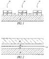
- the magnetic memory array of FIG. 1illustrates, in a basic way, the three functional layers of a TMR device.
- TMR devices 10work by electron tunneling from one magnetic layer to another through a thin barrier layer 12 .
- the tunneling probabilityis greatest when the magnetic layers 14 , 16 , on either side of the barrier layer 12 , have parallel magnetizations and least when the magnetizations are anti-parallel.
- these layersmust be electrically isolated from one another. Any short circuiting of the layers bypasses the data storage of the device.
- Copper conductors for MRAM arraysare currently preferred in order to reduce the likelihood of problems with electromigration caused by the high current density carried by the bit and word lines. Copper conducting lines are usually made using a damascene process.
- FIG. 1the copper conducting line 18 , in contact with the bottom of the TMR devices 10 , is shown in the plane of the paper.
- a thick insulating layeris deposited over the MRAM array. Trenches are etched into the insulating layer to expose the top surfaces of the TMR devices 10 . Copper is deposited to fill the trenches and make electrical contact to the TMR devices 10 .
- Top electrodes (not shown in FIG. 1 ) over the TMR devices 10are preferably also formed by damascene processing.
- trenchesare usually etched anisotropically through a patterned mask, overetching can occur both in the width of the trench and in the depth of the etch. If the etch is too deep, gaps develop along the sidewalls of the memory devices. Subsequent copper deposition fills the gaps and can short the memory devices. A more robust method of forming conducting lines over magnetic memory devices is needed.
- a method of forming a magnetic random access memoryis provided.
- a plurality of individual magnetic memory devices with cap layersare defined on a substrate.
- a continuous first insulator layeris provided over the substrate and the magnetic memory devices. Portions of the first insulator layer are removed at least over the magnetic memory devices and then the cap layers are selectively removed, thus exposing active top surfaces of the magnetic memory devices.
- Top conductorsare formed in contact with the active top surfaces of the magnetic memory devices.
- a method for forming a magnetoresistive memory on a semiconductor substrate having an underlying integrated circuit componentis provided.
- a plurality of protrusionscomprising magnetoresistive memory layers with a capping layer as an uppermost layer is formed.
- a conformal layer of spacer materialis deposited over the protrusions and a spacer etch is performed, thereby forming spacers along side surfaces of the protrusions.
- a layer of insulating materialis formed over the protrusions, the spacers and the substrate. The insulating material is removed at least over the protrusions, the capping layer is selectively etched away and a metallization process is performed to make contact to the magnetoresistive memory layers.
- a magnetic memory structurecomprises a plurality of magnetic memory stacks, each stack in a stud configuration. There is a first insulator layer around the magnetic memory stacks, and the top surfaces of the magnetic memory stacks are recessed below the top surface of the first insulator layer. There is a metal conductor in contact with the top surface of the magnetic memory stacks.
- FIG. 1is a cross section drawing of a portion of an array of TMR magnetic memory devices having stud configurations, in accordance with the prior art.
- FIG. 2is a cross-section drawing of blanket layers of a magnetic memory stack and a cap material, constructed in accordance with the preferred embodiments of the present invention.
- FIG. 3is a cross-section drawing of an individual magnetic memory device with a cap layer in a stud configuration as etched from the blanket layers of FIG. 2 .
- FIG. 4is a cross-section drawing of the memory device of FIG. 3 surrounded by a first insulator layer.
- FIG. 5is a cross-section drawing of the memory device of FIG. 4 with the cap removed and a top conductor, made by a standard metallization process, in contact with the device, in accordance with one arrangement.
- FIG. 6Ais a cross-section drawing of the memory device of FIG. 4 after a second insulator layer has been deposited and a trench has been etched into the second insulator layer, in accordance with another arrangement.
- FIG. 6Bis a cross-section drawing of the memory device of FIG. 6A after the cap has been removed and a top conductor, in contact with the device, has been made by a dual damascene process.
- FIG. 7Ais a cross-section drawing of an alternative embodiment for a dual damascene process wherein an etch stop layer has been deposited between the first insulator layer and the second insulator layer.
- FIG. 7Bis a cross-section drawing of the alternative embodiment of FIG. 7A after the etch stop layer has been removed from the bottom of the trench in the second insulator layer, the cap has been removed, and the top conductor has been formed.
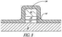
- FIG. 8is a cross-section drawing of the memory device of FIG. 3 , over which a layer of spacer material has been deposited, in accordance with another embodiment.
- FIG. 9is a cross-section drawing of the memory device of FIG. 8 after a spacer etch.
- FIG. 10is a cross-section drawing of the memory device of FIG. 9 surrounded by the first insulator layer.
- FIG. 11is a cross-section drawing of the memory device of FIG. 10 with the cap removed and a top conductor, made by a standard metallization process, in contact with the device.
- FIG. 12is a cross-section drawing of the memory device of FIG. 10 with the cap removed and a top conductor, made by a dual damascene process, in contact with the device according to a preferred embodiment.
- FIG. 13is a cross-section drawing of the memory device of FIG. 10 with the cap removed and a top conductor, made by a dual damascene process, in contact with the device according to an alternative embodiment wherein the second insulator layer has been overetched, and metal extends part way into the first insulator layer.
- the aforementioned needsare satisfied by the process of the present invention.
- the preferred embodimentsemploy a sacrificial cap over the active memory device.
- the capis more easily etched than the surrounding insulator material(s), resulting in good control in etching the trench for the top conductor with much less chance of an overetch.
- spacers with a low etch rateare used around the active memory device, so that even if an overetch does occur, the spacers are relatively unaffected, and the sides of the memory device remain protected by the spacers.
- FIG. 2is a starting point for the illustrated embodiments of the current invention.
- the embodimentsare illustrated for a TMR magnetic memory cell, having a top surface and an outside surface but the embodiments of the invention can be applied equally well to memory cells of other types.
- a metal conducting line 18preferably copper or aluminum, has been formed on or in a substrate (not shown). The conducting line 18 extends to the right and to the left of the page.
- a first stack 14 of magnetic and associated adjacent blanket layersis deposited.
- a thin tunneling barrier layer 12is deposited over the first stack 14 , and a second stack 16 of magnetic and associated adjacent blanket layers is deposited over the tunneling layer 12 , as is known in the art of TMR magnetic memory cell manufacture.
- a blanket cap layer 20is deposited over the second TMR material stack 16 .
- the cap material 20is selectively etchable relative to the top portion of the second TMR stack 16 .
- the cap materialcomprises a non-metal such as amorphous carbon, diamond-like carbon, amorphous silicon, silicon carbide, deposited by the BLOKTM (AMAT) process or a silicon-rich oxynitride, such as DARC (dielectric anti-reflective coating).
- FIG. 3shows one TMR memory cell stud 10 with the capping layer 20 after the blanket layers of FIG. 2 have been patterned and etched into an array of memory cells. Patterning and etching can be done by depositing a mask layer over the cap layer, then patterning the mask layer and etching the cap layer and the magnetic memory layers through exposed regions in the mask.
- a silicon oxide hard mask materialis one material suitable for the mask layer.
- a continuous first insulator or interlevel dielectric (ILD 1 ) layer 22has been deposited and planarized, preferably using chemical-mechanical planarization (CMP), to expose the top of the capping layer 20 .
- CMPchemical-mechanical planarization
- ILD 1 22comprises silicon oxide, formed by decomposition of TEOS (tetraethylorthosilicate).
- ILD 1 22is silicon nitride.
- the top portion of the top magnetic stack 16comprises metal, such as tantalum.
- the capping layer 20can undergo CMP without the ill effects described above.
- the capis not an active, functional part of the memory cell. Even if some of the cap 20 is removed during CMP, the underlying cell 10 remains intact.
- the materials preferred for the cap 20do not have a tendency to smear during CMP. Thus the cap material remains localized over the memory cell 10 .
- FIG. 5An embodiment that involves a standard metallization is shown in FIG. 5 .
- the cap 20has been removed.
- the cap 20is removed by an etch process that is preferential for the cap material over the ILD 1 22 .
- a preferential etchis performed to remove the cap 20 .
- the cap 20comprises amorphous or diamond-like carbon, it is preferable to remove it using an oxygen plasma.
- the cap 20comprises amorphous silicon, it is preferable to remove it using Cl, HBr, HI or NF 3 plasma.
- the cap 20comprises silicon carbide or a silicon-rich oxynitride, it is preferable to remove it using a halide chemistry having no carbon, such as Cl 2 or NF 3 .
- the cap 20comprises DARC (dielectric anti-reflective coating comprising a silicon-rich silicon oxynitride), it is preferable to remove it using NF 3 /Cl 2 , which has a 2:1 etch rate for DARC vs. silicon oxide from TEOS.
- DARCdielectric anti-reflective coating comprising a silicon-rich silicon oxynitride
- NF 3 /Cl 2which has a 2:1 etch rate for DARC vs. silicon oxide from TEOS.
- a metal layerpreferably comprising aluminum, is deposited, patterned and etched.
- the metal 24fills the region formerly occupied by the cap 20 .
- the portion of the patterned metal 24 above the top surface of the ILD 1 22comprises a top conductor line running into the page of FIG. 5 , making electrical connections along a row of cells 10 .
- a second insulating layer(not shown) can be deposited over conducting lines 24 , and processing can continue.
- the structure of the embodiment illustrated in FIG. 5comprises a multi-layer magnetic memory cell 10 , preferably a TMR memory cell, in contact at its bottom surface with a conducting line 18 , preferably comprising aluminum or copper.
- the thickness of the conducting line 18is between about 100 nm and 350 nm.
- the thickness of the multi-layer magnetic memory cell 10is between about 20 nm and 50 nm.
- the width of the cellis between about 150 nm and 500 nm.
- the cellis surrounded on its sides by an insulating layer 22 , preferably silicon oxide or silicon nitride.
- the insulating layer 22is taller than the memory cell 10 , having a thickness of between about 50 nm and 100 nm.
- the top surface of the memory cell 10is recessed from the top surface of the insulating layer 22 by between about 20 nm and 50 nm.
- the corners of the insulating layer 22 at the top of the recessare slightly rounded from the cap etch process.
- Metal 24preferably comprising aluminum, fills the recess between the memory cell 10 and the top of the insulating layer 22 , making electrical connection to the memory cell 10 , and forms a line extending over the top surface of the insulating layer 22 between about 10 nm and 50 nm on either side of the recess and connecting a row of memory cells 10 .
- the cross section of the metal line 24 over the memory cell 10has a T-shape.
- the top portion of the T-shape 24is wider than the memory cell 10 .
- the extra width in the metal line 24creates a magnetic field that is more effective in writing to the bit 10 than the field from a thinner metal line, but the selectively etchable cap reduces the rish of shorting despite the electrode width.
- ILD 1 22is deposited and planarized as described above for FIG. 4 .
- the cap 20is still in place.
- a second blanket insulating layer, ILD 2 26is deposited over ILD 1 22 .
- a trench 28is etched into ILD 2 26 , down to the top surface of the cap 20 and to the top surface of ILD 1 22 , and along a row of memory cells 10 into the page.
- the trench 28is wider than the cap 20 , as shown in FIG. 6A .
- a layer of metalpreferably copper, has been deposited to fill the opening over the memory cell 10 left by the cap 20 removal and to fill the trench 28 connecting a row of memory cells 10 .
- the trench 28may be lined with barrier and/or seed layers before being filled with metal.
- the top surface of ILD 2 26is planarized to remove excess metal and to leave a flat surface for further processing steps.
- the resulting top conducting line 30has a T-shaped cross section over the memory cells 10 , which, as discussed above, results in a more effective magnetic field at the bit.
- the structure illustrated in FIG. 6Bcomprises a multi-layer magnetic memory cell 10 , preferably a TMR memory cell, in contact at its bottom surface with a conducting line 18 , preferably comprising copper or aluminum.
- the thickness of the conducting line 18is between about 100 nm and 350 nm.
- the thickness of the multi-layer magnetic memory cell 10is between about 20 nm and 50 nm.
- the width of the cellis between about 150 nm and 500 nm.
- the cellis surrounded on its sides by an insulating layer 22 , preferably silicon oxide or silicon nitride.
- the insulating layer 22is taller than the memory cell 10 , having a thickness of between about 50 nm and 100 nm.
- the top surface of the memory cell 10is recessed from the top surface of the insulation by between about 20 nm and 50 nm.
- the corners of the insulating layer 22 at the top of the recessare slightly rounded.
- a second insulating layer 26preferably comprising silicon oxide or silicon nitride, and having a thickness between about 100 nm and 300 nm overlies the first insulating layer 22 .
- the width of the trenchis between about 50 nm and 1500 nm.
- the trench in the second insulating layer 26 and the recess between the magnetic memory cell 10 and the top of the first insulating layer 22are filled continuously by a conducting material 30 , preferably copper.
- the trench 28may be lined with barrier and/or seed layers before being filled with metal.
- the cross section of the conducting line 30has a T-shape in the region over the magnetic memory cell 10 .
- the top surface of the conducting line 30is coplanar with the top surface of the second insulating layer 26 .
- an etch stop layer 32is formed on the top surface of ILD 1 22 and the cap 20 before deposition of ILD 2 26 .
- the etch stop layer 32comprises a material that can be etched more slowly than ILD 2 26 , such as silicon carbide or some silicon nitrides.
- the etch ratedepends both on the material and the etchant.
- the etch stop layer 32can, in some arrangements, comprise the same material as the cap 20 .
- a trench 28is etched into ILD 2 26 down to the etch stop layer 32 along a row of memory cells 10 . As shown in FIG.
- etch stop layer 32is deposited to fill the opening over the memory cell 10 left by the cap 20 removal and to fill the trench 28 connecting a row of memory cells 10 .
- metal 30preferably copper, is deposited to fill the opening over the memory cell 10 left by the cap 20 removal and to fill the trench 28 connecting a row of memory cells 10 .
- the opening left by the cap 20 removal and the trench 28may be lined with barrier and/or seed layers before being filled with metal.
- the top surface of ILD 2 26is planarized to remove excess metal and to leave a flat surface for further processing steps.
- FIG. 7BThe embodiment illustrated in FIG. 7B is the same as the embodiment of FIG. 6B with one modification.
- An etch stop layer 32preferably silicon carbide or silicon nitride, having a thickness between about 10 nm and 300 nm, lies between the bottom surface of the second insulating layer 26 and the top surface of the first insulating layer 22 .
- the etch stop layer 32does not extend into the trench region that has been cut into the second insulating layer 26 , but is confined to the region under the second insulating layer 26 only.
- FIG. 8shows the memory cell 10 with cap 20 of FIG. 3 after a layer of spacer material 34 has been deposited conformally over an array of memory cells.
- the spacer material 34etches more slowly than both the cap material and ILD 1 .
- the etch ratedepends on both the material and the etchant.
- the spacer materialalso etches faster than the ILD 1 22 ( FIG. 10 ) to be deposited.
- the spacer materialcan comprise silicon carbide or silicon nitride.
- FIG. 9shows the memory cell 10 with cap 20 after an anisotropic spacer etch has been performed. Horizontal portions of spacer material layer 34 have been removed. Vertical portions of layer 34 remain to form a spacer 36 around the memory cell 10 and cap 20 .
- FIG. 9is a cross section drawing from approximately the center of the memory cell 10 and shows the spacer 36 only along two sides of the memory cell 10 and cap 20 . Actually, the spacer 36 forms a continuous covering all the way around the sides of the memory cell 10 and cap 20 .
- a first insulator layer or ILD 1 22has been deposited and planarized, much as was described for FIG. 4 above.
- the ILD 1 22etches slower than the spacer 36 .
- the ILD 1 22comprises a soft, reflowable oxide, such as an oxide deposited from TEOS (tetraethylorthosilicate).
- TEOStetraethylorthosilicate
- FIG. 11shows the memory cell 10 with spacer 36 after a standard metallization process.
- the cap 20has been removed by a preferential etch.
- the cap 20is removed completely by the etch process, and small amounts of the top surfaces of the spacer 36 and ILD 1 22 near the cap 20 have also been removed by the etch. Even thought the etch is preferential for removing the cap 20 , it has some effectiveness in etching the surrounding materials, such as the spacer 36 and ILD 1 22 .
- the spacer 36etches faster than the ILD 1 22 .
- a metal layer, preferably aluminum,has been deposited to fill the recess left after the etch process.
- the metal layerhas been patterned and etched to leave metal lines 30 perpendicular to the plane of the page, in electrical contact with the memory cell 10 and acting as a top conductor above ILD 1 22 , connecting a row of memory cells 10 .
- the electrode 30is wider than the memory cell 10 , which is better for flipping the bit 10 .
- Selective processingfacilitates a wider electrode without shorting out the memory cell from mask misalignment.
- a second insulating layer(not shown) can be deposited over the metal lines 30 .
- the structure of the embodiment illustrated in FIG. 11comprises a multi-layer magnetic memory cell 10 , preferably a TMR memory cell, in contact at its bottom surface with a conducting line 18 , preferably comprising aluminum or copper.
- the thickness of the conducting line 18is between about 100 nm and 350 nm.
- the thickness of the multi-layer magnetic memory cell 10is between about 20 nm and 50 nm.
- the width of the cellis between about 150 nm and 500 nm.
- the cellis surrounded on its sides by an insulating layer 22 , preferably silicon oxide or silicon nitride.
- the insulating layer 22is taller than the memory cell 10 , having a thickness of between about 50 nm and 100 nm.
- the top surface of the memory cell 10is recessed from the top surface of the insulation by between about 20 nm and 50 nm.
- the corners of the insulating layer 22 at the top of the recessare slightly rounded.
- Between the memory cell 10 and the surrounding insulating layer 22there is a spacer 36 , preferably comprising silicon carbide or silicon nitride.
- the spacer 36has a height that is between the height of the memory cell 10 and the height of the insulating layer 22 .
- the spacer 36is thickest at the bottom, adjacent to the conducting line 18 , and becomes more narrow as it reaches its full height. At the thickest part, the spacer 36 has a thickness between about 10 nm and 40 nm.
- a metal line 24preferably comprising aluminum, fills the recess between the memory cell 10 and the top of the insulating layer 22 , making electrical connection to the memory cell 10 and contacting the inside and top surfaces of the spacer 36 along the edges of the recess.
- the recessmay be lined with barrier and seed layers before being filled with metal.
- the metalextends over the top surface of the insulating layer 22 between about 10 nm and 50 nm on either side of the recess, thus providing a magnetic field that is better for flipping the bit 10 .
- FIG. 12Metallization by a dual damascene process is shown in FIG. 12 .
- ILD 1 22 deposition and planarization as shown in FIG. 10a second insulating layer, ILD 2 26 is formed.
- a trenchis etched into ILD 2 26 down to the surface of ILD 1 22 and the cap 20 .
- the cap 20is removed by a preferential etch, which also removes some small portion of the top surface of the spacer 36 and ILD 1 22 near the cap 20 .
- the etch rateis preferably fastest for the cap 20 , slower for the spacer 36 and slowest for ILD 1 22 .
- the structure of the embodiment illustrated in FIG. 12comprises a multi-layer magnetic memory cell 10 , preferably a TMR memory cell, in contact at its bottom surface with a conducting line 18 , preferably comprising copper or aluminum.
- the thickness of the conducting line 18is between about 100 nm and 350 nm.
- the thickness of the multi-layer magnetic memory cell 10is between about 20 nm and 50 nm.
- the width of the cell 10is between about 150 nm and 500 nm.
- the cell 10is surrounded on its sides by an insulating layer 22 , preferably silicon oxide or silicon nitride.
- the insulating layer 22is taller than the memory cell 10 , having a thickness of between about 500 nm and 1000 nm.
- the top surface of the memory cell 10is recessed from the top surface of the insulation by between about 20 nm and 50 nm.
- the corners of the insulating layer 22 at the top of the recessare slightly rounded.
- Between the memory cell 10 and the surrounding insulating layer 22there is a spacer 36 , preferably comprising silicon carbide or silicon nitride.
- the spacer 36has a height that is between the height of the memory cell 10 and the height of the insulating layer 22 .
- the spacer 36is thickest at the bottom, adjacent to the conducting line 18 , and becomes more narrow as it reaches its full height. At the thickest part, the spacer 36 has a thickness between about 10 nm and 40 nm.
- a second insulating layer 26preferably comprising silicon oxide or silicon nitride, and having a thickness between about 100 nm and 300 nm overlies the first insulating layer 22 .
- There is a trench in the second insulating layer directly over the memory cell 10preferably having a width greater than the combined width of the magnetic memory cell 10 and the spacer 36 .
- the width of the trenchis between about 300 nm and 1000 nm.
- the trench in the second insulating layer 26 and the recess between the magnetic memory cell 10 and the top of the first insulating layer 22are filled continuously by a conducting material 30 , preferably copper.
- the trench and the recessmay be lined with barrier and seed layers before being filled with metal.
- an etch stop layercan be formed over ILD 1 22 before deposition of ILD 2 26 in the structure of FIG. 12 as was shown for the non-spacer embodiment in FIGS. 7A–7B .
- FIG. 13Another embodiment of the current invention is shown in FIG. 13 , wherein the materials used in the structure and/or the etchants used are different than for FIG. 12 and therefore result in a different structure.
- the etchant used to form a trench in ILD 2 26also etches ILD 1 22 faster than it etches the spacer 36 .
- the etch rateis fastest for the cap layer 20 , slower for ILD 1 22 and slowest for the spacer 36 .
- the etched regionextends into ILD 1 22 along the outside surfaces of the spacer 36 due to the width of the overlying trench.
- the spacer 36 materialis more resistant to the etchant than is ILD 1 22 .
- the metal layerWhen the metal layer is deposited, it fills the overetched regions in addition to the recess left after the cap is removed and the trench etched into ILD 2 26 .
- the trench, the recess and the overetched regionsmay all be lined with barrier and/or seed layers before the metal is deposited. Even with the illustrated overetch, the memory device 10 is neither damaged nor shorted out, as it is insulated and protected by the spacer 36 that surrounds it.
- Table Isummarizes various possible combinations of materials and chemistries in accordance with the illustrated embodiments.
- Embodiment 1a 1b 2a 2b 3 4cap 20 amorphous C amorphous Si SiC (BLOK TM - DARC (Si-rich diamond-like C AMAT) oxynitride) ILD1 22 TEOS Si—N TEOS Si—N TEOS TEOS ILD2 26 TEOS Si—N TEOS Si—N TEOS TEOS etch stop 32 SiC or SiC SiC or SiC SiC of Si—N SiC or Si—N optional Si—N Si—N spacer 36 SiC or SiC SiC* Si—N SiC Si—N — Si—N etchant to oxygen plasma Cl, HBr, HI, NF 3 Cl 2 /NF 3 NF 3 /Cl 2 selectively (halide) plasmas no carbon remove cap 20
- the cap 20comprises amorphous carbon or diamond-like carbon.
- ILD 1 22 and ILD 2 26comprise silicon oxide formed from TEOS.
- the cap 20can be etched selectively using an oxygen plasma.
- the cap 20comprises amorphous carbon or diamond-like carbon.
- ILD 1 22 and ILD 2 26comprise silicon nitride.
- the cap 20can be etched selectively using an oxygen plasma.
- the cap 20comprises amorphous silicon.
- ILD 1 22 and ILD 2 26comprise silicon oxide formed from TEOS.
- the cap 20can be etched selectively using a halide plasma.
- the cap 20comprises amorphous silicon.
- ILD 1 22 and ILD 2 26comprise silicon nitride.
- the cap 20can be etched selectively using a halide plasma.
- the cap 20comprises silicon carbide.
- ILD 1 22 and ILD 2 26comprise silicon oxide formed from TEOS.
- the cap 20can be etched selectively using Cl 2 or NF 3 .
- the cap 20comprises DARC.
- ILD 1 22 and ILD 2 26comprise silicon oxide formed from TEOS.
- the cap 20can be etched selectively using at least one of NF 3 and Cl 2 .
- Optional etch stop 32 materials and spacer 36 materialsare also listed in Table I for each embodiment.
- etchingdepends on both the materials and the etchants. Thus, materials and etchants must be carefully chosen to produce the desired relative etching removal rates.
- the etchants for each embodiment in Table Ihave been chosen because they preferentially remove the associated cap 20 material relative to the associated insulating layers ILD 1 22 and ILD 2 26 .
Landscapes
- Engineering & Computer Science (AREA)
- Chemical & Material Sciences (AREA)
- Nanotechnology (AREA)
- Power Engineering (AREA)
- Crystallography & Structural Chemistry (AREA)
- Manufacturing & Machinery (AREA)
- Physics & Mathematics (AREA)
- Spectroscopy & Molecular Physics (AREA)
- Computer Hardware Design (AREA)
- Condensed Matter Physics & Semiconductors (AREA)
- General Physics & Mathematics (AREA)
- Semiconductor Memories (AREA)
- Mram Or Spin Memory Techniques (AREA)
- Internal Circuitry In Semiconductor Integrated Circuit Devices (AREA)
- Hall/Mr Elements (AREA)
Abstract
Description
| TABLE I | ||||||
| Embodiment | 1a | 1b | 2a | 2b | 3 | 4 |
| amorphous C | amorphous Si | SiC (BLOK ™ - | DARC (Si-rich | |
| diamond-like C | AMAT) | oxynitride) |
| ILD1 22 | TEOS | Si—N | TEOS | Si—N | TEOS | |
| ILD2 | ||||||
| 26 | TEOS | Si—N | TEOS | Si—N | TEOS | TEOS |
| etch stop 32 | SiC or | SiC | SiC or | SiC | SiC of Si—N | SiC or Si—N |
| optional | Si—N | Si— | ||||
| spacer | ||||||
| 36 | SiC or | SiC | SiC* Si—N | SiC | Si—N | — |
| Si—N |
| etchant to | oxygen plasma | Cl, HBr, HI, NF3 | Cl2/NF3 | NF3/Cl2 |
| selectively | (halide) plasmas | no | ||
| remove cap | ||||
| 20 | ||||
Claims (23)
Priority Applications (1)
| Application Number | Priority Date | Filing Date | Title |
|---|---|---|---|
| US10/856,356US7211849B2 (en) | 2002-04-30 | 2004-05-28 | Protective layers for MRAM devices |
Applications Claiming Priority (2)
| Application Number | Priority Date | Filing Date | Title |
|---|---|---|---|
| US10/135,921US6783995B2 (en) | 2002-04-30 | 2002-04-30 | Protective layers for MRAM devices |
| US10/856,356US7211849B2 (en) | 2002-04-30 | 2004-05-28 | Protective layers for MRAM devices |
Related Parent Applications (1)
| Application Number | Title | Priority Date | Filing Date |
|---|---|---|---|
| US10/135,921DivisionUS6783995B2 (en) | 2002-04-30 | 2002-04-30 | Protective layers for MRAM devices |
Publications (2)
| Publication Number | Publication Date |
|---|---|
| US20040264240A1 US20040264240A1 (en) | 2004-12-30 |
| US7211849B2true US7211849B2 (en) | 2007-05-01 |
Family
ID=29249570
Family Applications (2)
| Application Number | Title | Priority Date | Filing Date |
|---|---|---|---|
| US10/135,921Expired - LifetimeUS6783995B2 (en) | 2002-04-30 | 2002-04-30 | Protective layers for MRAM devices |
| US10/856,356Expired - LifetimeUS7211849B2 (en) | 2002-04-30 | 2004-05-28 | Protective layers for MRAM devices |
Family Applications Before (1)
| Application Number | Title | Priority Date | Filing Date |
|---|---|---|---|
| US10/135,921Expired - LifetimeUS6783995B2 (en) | 2002-04-30 | 2002-04-30 | Protective layers for MRAM devices |
Country Status (10)
| Country | Link |
|---|---|
| US (2) | US6783995B2 (en) |
| EP (2) | EP1793400B1 (en) |
| JP (1) | JP4378631B2 (en) |
| KR (2) | KR100755240B1 (en) |
| CN (1) | CN100338700C (en) |
| AT (1) | ATE363720T1 (en) |
| AU (1) | AU2003239168A1 (en) |
| DE (1) | DE60314129T2 (en) |
| TW (1) | TWI238439B (en) |
| WO (1) | WO2003094182A1 (en) |
Cited By (9)
| Publication number | Priority date | Publication date | Assignee | Title |
|---|---|---|---|---|
| US20160380183A1 (en)* | 2015-06-25 | 2016-12-29 | Taiwan Semiconductor Manufacturing Co., Ltd. | Techniques for mram mtj top electrode connection |
| US20170047374A1 (en)* | 2015-08-10 | 2017-02-16 | Qualcomm Incorporated | Metallization process for a memory device |
| US9647033B2 (en) | 2014-12-22 | 2017-05-09 | Samsung Electronics Co., Ltd. | Methods of manufacturing magnetic memory device having a magnetic tunnel junction pattern |
| US11195993B2 (en)* | 2019-09-16 | 2021-12-07 | International Business Machines Corporation | Encapsulation topography-assisted self-aligned MRAM top contact |
| US11251368B2 (en) | 2020-04-20 | 2022-02-15 | International Business Machines Corporation | Interconnect structures with selective capping layer |
| US12120963B2 (en) | 2021-09-24 | 2024-10-15 | International Business Machines Corporation | Contact structure formation for memory devices |
| US12133473B2 (en) | 2021-09-24 | 2024-10-29 | International Business Machines Corporation | Contact structure formation for memory devices |
| US12349597B2 (en) | 2021-09-27 | 2025-07-01 | International Business Machines Corporation | Conical magnetic random access memory pillar structures |
| US12402536B2 (en) | 2022-05-31 | 2025-08-26 | International Business Machines Corporation | Magneto-resistive random access memory with hemispherical top electrode |
Families Citing this family (56)
| Publication number | Priority date | Publication date | Assignee | Title |
|---|---|---|---|---|
| US6770491B2 (en)* | 2002-08-07 | 2004-08-03 | Micron Technology, Inc. | Magnetoresistive memory and method of manufacturing the same |
| US7205598B2 (en)* | 2002-08-29 | 2007-04-17 | Micron Technology, Inc. | Random access memory device utilizing a vertically oriented select transistor |
| KR100496860B1 (en)* | 2002-09-19 | 2005-06-22 | 삼성전자주식회사 | Magneto-resistive memory device and method for fabricating the same |
| US6881351B2 (en)* | 2003-04-22 | 2005-04-19 | Freescale Semiconductor, Inc. | Methods for contacting conducting layers overlying magnetoelectronic elements of MRAM devices |
| US7183130B2 (en)* | 2003-07-29 | 2007-02-27 | International Business Machines Corporation | Magnetic random access memory and method of fabricating thereof |
| US7112454B2 (en)* | 2003-10-14 | 2006-09-26 | Micron Technology, Inc. | System and method for reducing shorting in memory cells |
| JP2005260082A (en)* | 2004-03-12 | 2005-09-22 | Toshiba Corp | Magnetic random access memory |
| US7045368B2 (en)* | 2004-05-19 | 2006-05-16 | Headway Technologies, Inc. | MRAM cell structure and method of fabrication |
| US7374952B2 (en)* | 2004-06-17 | 2008-05-20 | Infineon Technologies Ag | Methods of patterning a magnetic stack of a magnetic memory cell and structures thereof |
| US7368299B2 (en)* | 2004-07-14 | 2008-05-06 | Infineon Technologies Ag | MTJ patterning using free layer wet etching and lift off techniques |
| KR100975803B1 (en) | 2004-07-16 | 2010-08-16 | 헤드웨이 테크놀로지스 인코포레이티드 | A method of forming an MTV MRM cell, an array of MTV MRM cells, and an MTM MRM cell |
| US7067330B2 (en) | 2004-07-16 | 2006-06-27 | Headway Technologies, Inc. | Magnetic random access memory array with thin conduction electrical read and write lines |
| US7397077B2 (en)* | 2004-09-02 | 2008-07-08 | Samsung Electronics Co., Ltd. | Magnetic memory devices having patterned heater layers therein that utilize thermally conductive sidewall materials to increase heat transfer when writing memory data |
| TWI252559B (en)* | 2004-12-31 | 2006-04-01 | Ind Tech Res Inst | Method for connecting magnetoelectronic element with conductive line |
| US7399646B2 (en)* | 2005-08-23 | 2008-07-15 | International Business Machines Corporation | Magnetic devices and techniques for formation thereof |
| US20070072311A1 (en)* | 2005-09-28 | 2007-03-29 | Northern Lights Semiconductor Corp. | Interconnect for a GMR Stack Layer and an Underlying Conducting Layer |
| US7816718B2 (en)* | 2005-09-28 | 2010-10-19 | Northern Lights Semiconductor Corp. | Interconnect for a GMR memory cells and an underlying conductive layer |
| US7880249B2 (en)* | 2005-11-30 | 2011-02-01 | Magic Technologies, Inc. | Spacer structure in MRAM cell and method of its fabrication |
| US7371636B2 (en)* | 2005-12-14 | 2008-05-13 | Hynix Semiconductor Inc. | Method for fabricating storage node contact hole of semiconductor device |
| US7419891B1 (en)* | 2006-02-13 | 2008-09-02 | Western Digital (Fremont), Llc | Method and system for providing a smaller critical dimension magnetic element utilizing a single layer mask |
| US8141235B1 (en) | 2006-06-09 | 2012-03-27 | Western Digital (Fremont), Llc | Method for manufacturing a perpendicular magnetic recording transducers |
| WO2008155832A1 (en)* | 2007-06-20 | 2008-12-24 | Fujitsu Microelectronics Limited | Semiconductor device, and its manufacturing method |
| KR100854863B1 (en)* | 2007-06-29 | 2008-08-28 | 주식회사 하이닉스반도체 | Manufacturing method of semiconductor device |
| US9136463B2 (en)* | 2007-11-20 | 2015-09-15 | Qualcomm Incorporated | Method of forming a magnetic tunnel junction structure |
| US7781231B2 (en)* | 2008-03-07 | 2010-08-24 | Qualcomm Incorporated | Method of forming a magnetic tunnel junction device |
| JP5175750B2 (en)* | 2009-01-19 | 2013-04-03 | 株式会社日立製作所 | Manufacturing method of semiconductor integrated circuit device using magnetic memory element |
| US9099118B1 (en) | 2009-05-26 | 2015-08-04 | Western Digital (Fremont), Llc | Dual damascene process for producing a PMR write pole |
| US8486285B2 (en) | 2009-08-20 | 2013-07-16 | Western Digital (Fremont), Llc | Damascene write poles produced via full film plating |
| CN102446541B (en)* | 2010-10-13 | 2014-03-12 | 中芯国际集成电路制造(上海)有限公司 | Magnetic random access memory and manufacturing method thereof |
| US8962493B2 (en)* | 2010-12-13 | 2015-02-24 | Crocus Technology Inc. | Magnetic random access memory cells having improved size and shape characteristics |
| KR101222117B1 (en) | 2011-02-25 | 2013-01-14 | 에스케이하이닉스 주식회사 | Method for fabricating sttram |
| US20150021724A1 (en)* | 2011-04-11 | 2015-01-22 | Magsil Corporation | Self contacting bit line to mram cell |
| KR20150075602A (en)* | 2013-12-26 | 2015-07-06 | 삼성전자주식회사 | Magnetoresistive random access device and method of manufacturing the same |
| US9318696B2 (en)* | 2014-03-03 | 2016-04-19 | Qualcomm Incorporated | Self-aligned top contact for MRAM fabrication |
| US9666790B2 (en) | 2015-07-17 | 2017-05-30 | Taiwan Semiconductor Manufacturing Co., Ltd. | Manufacturing techniques and corresponding devices for magnetic tunnel junction devices |
| KR102326547B1 (en) | 2015-08-19 | 2021-11-15 | 삼성전자주식회사 | Magnetoresistive random access device and method of manufacturing the same |
| KR102444236B1 (en)* | 2015-08-25 | 2022-09-16 | 삼성전자주식회사 | Magnetic element and manufacturing method thereof |
| KR101726404B1 (en) | 2015-11-16 | 2017-04-12 | 중소기업은행 | Apparatus for predicting customer who will stop transaction and method thereof |
| US9647200B1 (en) | 2015-12-07 | 2017-05-09 | International Business Machines Corporation | Encapsulation of magnetic tunnel junction structures in organic photopatternable dielectric material |
| US9660179B1 (en)* | 2015-12-16 | 2017-05-23 | International Business Machines Corporation | Enhanced coercivity in MTJ devices by contact depth control |
| US9515252B1 (en) | 2015-12-29 | 2016-12-06 | International Business Machines Corporation | Low degradation MRAM encapsulation process using silicon-rich silicon nitride film |
| US9698339B1 (en) | 2015-12-29 | 2017-07-04 | International Business Machines Corporation | Magnetic tunnel junction encapsulation using hydrogenated amorphous semiconductor material |
| US9859156B2 (en)* | 2015-12-30 | 2018-01-02 | Taiwan Semiconductor Manufacturing Co., Ltd. | Interconnection structure with sidewall dielectric protection layer |
| US10454021B2 (en) | 2016-01-29 | 2019-10-22 | Taiwan Semiconductor Manufacturing Company Ltd. | Semiconductor structure and method of manufacturing the same |
| CN107785484B (en)* | 2016-08-25 | 2021-08-06 | 中电海康集团有限公司 | Method for manufacturing memory by self-aligned photoetching corrosion |
| CN107785483B (en)* | 2016-08-25 | 2021-06-01 | 中电海康集团有限公司 | Method for manufacturing magnetic random access memory |
| CN109980081B (en)* | 2017-12-28 | 2023-10-20 | 中电海康集团有限公司 | Method for manufacturing MRAM device capable of stopping polishing automatically and MRAM device |
| CN109994394B (en)* | 2017-12-29 | 2021-05-28 | 中电海康集团有限公司 | Method for flattening MTJ (magnetic tunnel junction) unit in MRAM (magnetic random Access memory) device and MRAM device |
| US11997931B2 (en) | 2018-10-31 | 2024-05-28 | Taiwan Semiconductor Manufacturing Company, Ltd. | Bar-type magnetoresistive random access memory cell |
| CN109872994B (en)* | 2019-03-07 | 2021-09-03 | 上海华虹宏力半导体制造有限公司 | Split-gate flash memory and preparation method thereof |
| US11744083B2 (en) | 2019-04-12 | 2023-08-29 | International Business Machines Corporation | Fabrication of embedded memory devices utilizing a self assembled monolayer |
| US11094585B2 (en)* | 2019-07-08 | 2021-08-17 | Globalfoundries U.S. Inc. | Methods of forming a conductive contact structure to a top electrode of an embedded memory device on an IC product and a corresponding IC product |
| US11121308B2 (en) | 2019-10-15 | 2021-09-14 | Taiwan Semiconductor Manufacturing Company, Ltd. | Sidewall spacer structure for memory cell |
| FR3104320B1 (en)* | 2019-12-06 | 2024-12-13 | Commissariat Energie Atomique | Interconnection structure of an integrated circuit |
| US11985906B2 (en)* | 2020-05-29 | 2024-05-14 | Taiwan Semiconductor Manufacturing Company Limited | Low-resistance contact to top electrodes for memory cells and methods for forming the same |
| US11844291B2 (en) | 2021-06-21 | 2023-12-12 | United Microelectronics Corp. | Semiconductor memory device and fabrication method thereof |
Citations (75)
| Publication number | Priority date | Publication date | Assignee | Title |
|---|---|---|---|---|
| US3623032A (en) | 1970-02-16 | 1971-11-23 | Honeywell Inc | Keeper configuration for a thin-film memory |
| US3623035A (en) | 1968-02-02 | 1971-11-23 | Fuji Electric Co Ltd | Magnetic memory matrix and process for its production |
| US3816909A (en) | 1969-04-30 | 1974-06-18 | Hitachi Chemical Co Ltd | Method of making a wire memory plane |
| US3947831A (en) | 1972-12-11 | 1976-03-30 | Kokusai Denshin Denwa Kabushiki Kaisha | Word arrangement matrix memory of high bit density having a magnetic flux keeper |
| US4044330A (en) | 1976-03-30 | 1977-08-23 | Honeywell Information Systems, Inc. | Power strobing to achieve a tri state |
| US4060794A (en) | 1976-03-31 | 1977-11-29 | Honeywell Information Systems Inc. | Apparatus and method for generating timing signals for latched type memories |
| US4158891A (en) | 1975-08-18 | 1979-06-19 | Honeywell Information Systems Inc. | Transparent tri state latch |
| US4455626A (en) | 1983-03-21 | 1984-06-19 | Honeywell Inc. | Thin film memory with magnetoresistive read-out |
| US4731757A (en) | 1986-06-27 | 1988-03-15 | Honeywell Inc. | Magnetoresistive memory including thin film storage cells having tapered ends |
| US4780848A (en) | 1986-06-03 | 1988-10-25 | Honeywell Inc. | Magnetoresistive memory with multi-layer storage cells having layers of limited thickness |
| US4801883A (en) | 1986-06-02 | 1989-01-31 | The Regents Of The University Of California | Integrated-circuit one-way isolation coupler incorporating one or several carrier-domain magnetometers |
| US4945397A (en) | 1986-12-08 | 1990-07-31 | Honeywell Inc. | Resistive overlayer for magnetic films |
| US5039655A (en) | 1989-07-28 | 1991-08-13 | Ampex Corporation | Thin film memory device having superconductor keeper for eliminating magnetic domain creep |
| US5064499A (en) | 1990-04-09 | 1991-11-12 | Honeywell Inc. | Inductively sensed magnetic memory manufacturing method |
| US5140549A (en) | 1990-04-09 | 1992-08-18 | Honeywell Inc. | Inductively sensed magnetic memory |
| US5496759A (en) | 1994-12-29 | 1996-03-05 | Honeywell Inc. | Highly producible magnetoresistive RAM process |
| US5547599A (en) | 1989-03-17 | 1996-08-20 | Raytheon Company | Ferrite/epoxy film |
| US5569617A (en) | 1995-12-21 | 1996-10-29 | Honeywell Inc. | Method of making integrated spacer for magnetoresistive RAM |
| US5587943A (en) | 1995-02-13 | 1996-12-24 | Integrated Microtransducer Electronics Corporation | Nonvolatile magnetoresistive memory with fully closed flux operation |
| EP0776011A2 (en) | 1995-11-24 | 1997-05-28 | Motorola, Inc. | Magnetic memory and method therefor |
| US5650958A (en) | 1996-03-18 | 1997-07-22 | International Business Machines Corporation | Magnetic tunnel junctions with controlled magnetic response |
| US5691228A (en) | 1996-01-18 | 1997-11-25 | Micron Technology, Inc. | Semiconductor processing method of making a hemispherical grain (HSG) polysilicon layer |
| US5701222A (en) | 1995-09-11 | 1997-12-23 | International Business Machines Corporation | Spin valve sensor with antiparallel magnetization of pinned layers |
| US5721171A (en) | 1996-02-29 | 1998-02-24 | Micron Technology, Inc. | Method for forming controllable surface enhanced three dimensional objects |
| US5726498A (en) | 1995-05-26 | 1998-03-10 | International Business Machines Corporation | Wire shape conferring reduced crosstalk and formation methods |
| US5741435A (en) | 1995-08-08 | 1998-04-21 | Nano Systems, Inc. | Magnetic memory having shape anisotropic magnetic elements |
| US5744398A (en) | 1996-07-31 | 1998-04-28 | Ig Semicon Co., Ltd. | Method of forming electrode of semiconductor device |
| WO1998020496A1 (en) | 1996-11-08 | 1998-05-14 | Nonvolatile Electronics, Incorporated | Spin dependent tunneling memory |
| US5756366A (en) | 1995-12-21 | 1998-05-26 | Honeywell Inc. | Magnetic hardening of bit edges of magnetoresistive RAM |
| US5756394A (en) | 1995-08-23 | 1998-05-26 | Micron Technology, Inc. | Self-aligned silicide strap connection of polysilicon layers |
| US5792687A (en) | 1996-08-01 | 1998-08-11 | Vanguard International Semiconductor Corporation | Method for fabricating high density integrated circuits using oxide and polysilicon spacers |
| US5795823A (en) | 1995-06-07 | 1998-08-18 | Advanced Micro Devices, Inc. | Self aligned via dual damascene |
| US5851875A (en) | 1997-07-14 | 1998-12-22 | Micron Technology, Inc. | Process for forming capacitor array structure for semiconductor devices |
| US5861328A (en) | 1996-10-07 | 1999-01-19 | Motorola, Inc. | Method of fabricating GMR devices |
| US5869389A (en) | 1996-01-18 | 1999-02-09 | Micron Technology, Inc. | Semiconductor processing method of providing a doped polysilicon layer |
| US5899742A (en) | 1997-12-22 | 1999-05-04 | Sun; Shih-Wei | Manufacturing method for self-aligned local interconnects and contacts simultaneously |
| US5926394A (en) | 1996-09-30 | 1999-07-20 | Intel Corporation | Method and apparatus for regulating the voltage supplied to an integrated circuit |
| US5939758A (en) | 1996-11-25 | 1999-08-17 | Mitsubishi Denki Kabushiki Kaisha | Semiconductor device with gate electrodes having conductive films |
| US5945350A (en) | 1996-09-13 | 1999-08-31 | Micron Technology, Inc. | Methods for use in formation of titanium nitride interconnects and interconnects formed using same |
| US5956267A (en) | 1997-12-18 | 1999-09-21 | Honeywell Inc | Self-aligned wordline keeper and method of manufacture therefor |
| US5982658A (en) | 1997-10-31 | 1999-11-09 | Honeywell Inc. | MRAM design to reduce dissimilar nearest neighbor effects |
| US5994193A (en) | 1998-02-04 | 1999-11-30 | Advanced Micro Devices, Inc. | Method of making high performance MOSFET with integrated poly/metal gate electrode |
| JP2000030222A (en) | 1998-07-08 | 2000-01-28 | Fujitsu Ltd | Magnetic sensor |
| US6028786A (en) | 1997-04-28 | 2000-02-22 | Canon Kabushiki Kaisha | Magnetic memory element having coupled magnetic layers forming closed magnetic circuit |
| DE19836567A1 (en) | 1998-08-12 | 2000-02-24 | Siemens Ag | Memory cell structure with magneto-resistive memory elements comprises a magnetizable yoke surrounding one of the intersecting lines at a memory element location |
| WO2000019440A2 (en) | 1998-09-30 | 2000-04-06 | Infineon Technologies Ag | Magnetoresistive memory with low current density |
| US6048739A (en) | 1997-12-18 | 2000-04-11 | Honeywell Inc. | Method of manufacturing a high density magnetic memory device |
| US6100185A (en) | 1998-08-14 | 2000-08-08 | Micron Technology, Inc. | Semiconductor processing method of forming a high purity <200> grain orientation tin layer and semiconductor processing method of forming a conductive interconnect line |
| US6110812A (en) | 1999-05-11 | 2000-08-29 | Promos Technologies, Inc. | Method for forming polycide gate |
| US6130145A (en) | 1998-01-21 | 2000-10-10 | Siemens Aktiengesellschaft | Insitu doped metal policide |
| US6136705A (en) | 1998-10-22 | 2000-10-24 | National Semiconductor Corporation | Self-aligned dual thickness cobalt silicide layer formation process |
| US6153443A (en) | 1998-12-21 | 2000-11-28 | Motorola, Inc. | Method of fabricating a magnetic random access memory |
| US6156630A (en) | 1997-08-22 | 2000-12-05 | Micron Technology, Inc. | Titanium boride gate electrode and interconnect and methods regarding same |
| US6165803A (en) | 1999-05-17 | 2000-12-26 | Motorola, Inc. | Magnetic random access memory and fabricating method thereof |
| US6174737B1 (en) | 1998-08-31 | 2001-01-16 | Motorola, Inc. | Magnetic random access memory and fabricating method thereof |
| US6174764B1 (en) | 1997-05-12 | 2001-01-16 | Micron Technology, Inc. | Process for manufacturing integrated circuit SRAM |
| US6211054B1 (en) | 1999-06-01 | 2001-04-03 | Micron Technology, Inc. | Method of forming a conductive line and method of forming a local interconnect |
| US6211090B1 (en) | 2000-03-21 | 2001-04-03 | Motorola, Inc. | Method of fabricating flux concentrating layer for use with magnetoresistive random access memories |
| US6218302B1 (en)* | 1998-07-21 | 2001-04-17 | Motorola Inc. | Method for forming a semiconductor device |
| US6255701B1 (en) | 1995-11-06 | 2001-07-03 | Seiko Epson Corporation | Semiconductor device containing local interconnection and method of manufacturing the same |
| US6338899B1 (en) | 1998-06-30 | 2002-01-15 | Kabushiki Kaisha Toshiba | Magnetoresistance effect element, magnetic head, magnetic head assembly, magnetic storage system |
| US6358756B1 (en) | 2001-02-07 | 2002-03-19 | Micron Technology, Inc. | Self-aligned, magnetoresistive random-access memory (MRAM) structure utilizing a spacer containment scheme |
| US20020041514A1 (en) | 1999-02-26 | 2002-04-11 | Ulrich Scheler | Memory cell configuration and method for its production |
| US20020048946A1 (en) | 1999-04-14 | 2002-04-25 | Tang Sanh D. | Local interconnect structures for integrated circuits and methods for making the same |
| US6379978B2 (en) | 1998-07-15 | 2002-04-30 | Infineon Technologies Ag | Memory cell configuration in which an electrical resistance of a memory element represents an information item and can be influenced by a magnetic field, and method for fabricating it |
| US6392922B1 (en) | 2000-08-14 | 2002-05-21 | Micron Technology, Inc. | Passivated magneto-resistive bit structure and passivation method therefor |
| US6391658B1 (en) | 1999-10-26 | 2002-05-21 | International Business Machines Corporation | Formation of arrays of microelectronic elements |
| US6440753B1 (en)* | 2001-01-24 | 2002-08-27 | Infineon Technologies North America Corp. | Metal hard mask for ILD RIE processing of semiconductor memory devices to prevent oxidation of conductive lines |
| US6485989B1 (en) | 2001-08-30 | 2002-11-26 | Micron Technology, Inc. | MRAM sense layer isolation |
| US6500710B2 (en) | 1999-06-15 | 2002-12-31 | Fujitsu Limited | Method of manufacturing a nonvolatile semiconductor memory device |
| US6518071B1 (en)* | 2002-03-28 | 2003-02-11 | Motorola, Inc. | Magnetoresistive random access memory device and method of fabrication thereof |
| US6555858B1 (en)* | 2000-11-15 | 2003-04-29 | Motorola, Inc. | Self-aligned magnetic clad write line and its method of formation |
| US6627913B2 (en)* | 2001-09-10 | 2003-09-30 | Micron Technology, Inc. | Insulation of an MRAM device through a self-aligned spacer |
| US6630718B1 (en) | 1999-07-26 | 2003-10-07 | Micron Technology, Inc. | Transistor gate and local interconnect |
| US6754053B2 (en)* | 2001-03-30 | 2004-06-22 | Kabushiki Kaisha Toshiba | Magnetoresistance effect element, magnetic head and magnetic reproducing apparatus |
Family Cites Families (1)
| Publication number | Priority date | Publication date | Assignee | Title |
|---|---|---|---|---|
| US6025786A (en)* | 1998-05-06 | 2000-02-15 | Trw Inc. | Transmitter for remote convenience system having coiled, extendable antenna |
- 2002
- 2002-04-30USUS10/135,921patent/US6783995B2/ennot_activeExpired - Lifetime
- 2003
- 2003-04-21JPJP2004502311Apatent/JP4378631B2/ennot_activeExpired - Lifetime
- 2003-04-21EPEP07005378.0Apatent/EP1793400B1/ennot_activeExpired - Lifetime
- 2003-04-21AUAU2003239168Apatent/AU2003239168A1/ennot_activeAbandoned
- 2003-04-21EPEP03733885Apatent/EP1500116B1/ennot_activeExpired - Lifetime
- 2003-04-21KRKR1020067019755Apatent/KR100755240B1/ennot_activeExpired - Lifetime
- 2003-04-21ATAT03733885Tpatent/ATE363720T1/ennot_activeIP Right Cessation
- 2003-04-21KRKR1020047017428Apatent/KR100692417B1/ennot_activeExpired - Lifetime
- 2003-04-21CNCNB038115417Apatent/CN100338700C/ennot_activeExpired - Lifetime
- 2003-04-21DEDE60314129Tpatent/DE60314129T2/ennot_activeExpired - Lifetime
- 2003-04-21WOPCT/US2003/012675patent/WO2003094182A1/enactiveIP Right Grant
- 2003-04-22TWTW092109371Apatent/TWI238439B/ennot_activeIP Right Cessation
- 2004
- 2004-05-28USUS10/856,356patent/US7211849B2/ennot_activeExpired - Lifetime
Patent Citations (77)
| Publication number | Priority date | Publication date | Assignee | Title |
|---|---|---|---|---|
| US3623035A (en) | 1968-02-02 | 1971-11-23 | Fuji Electric Co Ltd | Magnetic memory matrix and process for its production |
| US3816909A (en) | 1969-04-30 | 1974-06-18 | Hitachi Chemical Co Ltd | Method of making a wire memory plane |
| US3623032A (en) | 1970-02-16 | 1971-11-23 | Honeywell Inc | Keeper configuration for a thin-film memory |
| US3947831A (en) | 1972-12-11 | 1976-03-30 | Kokusai Denshin Denwa Kabushiki Kaisha | Word arrangement matrix memory of high bit density having a magnetic flux keeper |
| US4158891A (en) | 1975-08-18 | 1979-06-19 | Honeywell Information Systems Inc. | Transparent tri state latch |
| US4044330A (en) | 1976-03-30 | 1977-08-23 | Honeywell Information Systems, Inc. | Power strobing to achieve a tri state |
| US4060794A (en) | 1976-03-31 | 1977-11-29 | Honeywell Information Systems Inc. | Apparatus and method for generating timing signals for latched type memories |
| US4455626A (en) | 1983-03-21 | 1984-06-19 | Honeywell Inc. | Thin film memory with magnetoresistive read-out |
| US4801883A (en) | 1986-06-02 | 1989-01-31 | The Regents Of The University Of California | Integrated-circuit one-way isolation coupler incorporating one or several carrier-domain magnetometers |
| US4849695A (en) | 1986-06-02 | 1989-07-18 | University Of California | Null-detection magnetometers |
| US4780848A (en) | 1986-06-03 | 1988-10-25 | Honeywell Inc. | Magnetoresistive memory with multi-layer storage cells having layers of limited thickness |
| US4731757A (en) | 1986-06-27 | 1988-03-15 | Honeywell Inc. | Magnetoresistive memory including thin film storage cells having tapered ends |
| US4945397A (en) | 1986-12-08 | 1990-07-31 | Honeywell Inc. | Resistive overlayer for magnetic films |
| US5547599A (en) | 1989-03-17 | 1996-08-20 | Raytheon Company | Ferrite/epoxy film |
| US5039655A (en) | 1989-07-28 | 1991-08-13 | Ampex Corporation | Thin film memory device having superconductor keeper for eliminating magnetic domain creep |
| US5140549A (en) | 1990-04-09 | 1992-08-18 | Honeywell Inc. | Inductively sensed magnetic memory |
| US5064499A (en) | 1990-04-09 | 1991-11-12 | Honeywell Inc. | Inductively sensed magnetic memory manufacturing method |
| US5496759A (en) | 1994-12-29 | 1996-03-05 | Honeywell Inc. | Highly producible magnetoresistive RAM process |
| US5587943A (en) | 1995-02-13 | 1996-12-24 | Integrated Microtransducer Electronics Corporation | Nonvolatile magnetoresistive memory with fully closed flux operation |
| US5726498A (en) | 1995-05-26 | 1998-03-10 | International Business Machines Corporation | Wire shape conferring reduced crosstalk and formation methods |
| US5795823A (en) | 1995-06-07 | 1998-08-18 | Advanced Micro Devices, Inc. | Self aligned via dual damascene |
| US5741435A (en) | 1995-08-08 | 1998-04-21 | Nano Systems, Inc. | Magnetic memory having shape anisotropic magnetic elements |
| US5756394A (en) | 1995-08-23 | 1998-05-26 | Micron Technology, Inc. | Self-aligned silicide strap connection of polysilicon layers |
| US5701222A (en) | 1995-09-11 | 1997-12-23 | International Business Machines Corporation | Spin valve sensor with antiparallel magnetization of pinned layers |
| US6255701B1 (en) | 1995-11-06 | 2001-07-03 | Seiko Epson Corporation | Semiconductor device containing local interconnection and method of manufacturing the same |
| EP0776011A2 (en) | 1995-11-24 | 1997-05-28 | Motorola, Inc. | Magnetic memory and method therefor |
| US5569617A (en) | 1995-12-21 | 1996-10-29 | Honeywell Inc. | Method of making integrated spacer for magnetoresistive RAM |
| US5756366A (en) | 1995-12-21 | 1998-05-26 | Honeywell Inc. | Magnetic hardening of bit edges of magnetoresistive RAM |
| US5691228A (en) | 1996-01-18 | 1997-11-25 | Micron Technology, Inc. | Semiconductor processing method of making a hemispherical grain (HSG) polysilicon layer |
| US5869389A (en) | 1996-01-18 | 1999-02-09 | Micron Technology, Inc. | Semiconductor processing method of providing a doped polysilicon layer |
| US5721171A (en) | 1996-02-29 | 1998-02-24 | Micron Technology, Inc. | Method for forming controllable surface enhanced three dimensional objects |
| US5882979A (en) | 1996-02-29 | 1999-03-16 | Micron Technology, Inc. | Method for forming controllable surface enhanced three dimensional objects |
| US5650958A (en) | 1996-03-18 | 1997-07-22 | International Business Machines Corporation | Magnetic tunnel junctions with controlled magnetic response |
| US5744398A (en) | 1996-07-31 | 1998-04-28 | Ig Semicon Co., Ltd. | Method of forming electrode of semiconductor device |
| US5792687A (en) | 1996-08-01 | 1998-08-11 | Vanguard International Semiconductor Corporation | Method for fabricating high density integrated circuits using oxide and polysilicon spacers |
| US5945350A (en) | 1996-09-13 | 1999-08-31 | Micron Technology, Inc. | Methods for use in formation of titanium nitride interconnects and interconnects formed using same |
| US5926394A (en) | 1996-09-30 | 1999-07-20 | Intel Corporation | Method and apparatus for regulating the voltage supplied to an integrated circuit |
| US5861328A (en) | 1996-10-07 | 1999-01-19 | Motorola, Inc. | Method of fabricating GMR devices |
| WO1998020496A1 (en) | 1996-11-08 | 1998-05-14 | Nonvolatile Electronics, Incorporated | Spin dependent tunneling memory |
| US5939758A (en) | 1996-11-25 | 1999-08-17 | Mitsubishi Denki Kabushiki Kaisha | Semiconductor device with gate electrodes having conductive films |
| US6028786A (en) | 1997-04-28 | 2000-02-22 | Canon Kabushiki Kaisha | Magnetic memory element having coupled magnetic layers forming closed magnetic circuit |
| US6174764B1 (en) | 1997-05-12 | 2001-01-16 | Micron Technology, Inc. | Process for manufacturing integrated circuit SRAM |
| US5851875A (en) | 1997-07-14 | 1998-12-22 | Micron Technology, Inc. | Process for forming capacitor array structure for semiconductor devices |
| US6156630A (en) | 1997-08-22 | 2000-12-05 | Micron Technology, Inc. | Titanium boride gate electrode and interconnect and methods regarding same |
| US5982658A (en) | 1997-10-31 | 1999-11-09 | Honeywell Inc. | MRAM design to reduce dissimilar nearest neighbor effects |
| US5956267A (en) | 1997-12-18 | 1999-09-21 | Honeywell Inc | Self-aligned wordline keeper and method of manufacture therefor |
| US6048739A (en) | 1997-12-18 | 2000-04-11 | Honeywell Inc. | Method of manufacturing a high density magnetic memory device |
| US5899742A (en) | 1997-12-22 | 1999-05-04 | Sun; Shih-Wei | Manufacturing method for self-aligned local interconnects and contacts simultaneously |
| US6130145A (en) | 1998-01-21 | 2000-10-10 | Siemens Aktiengesellschaft | Insitu doped metal policide |
| US5994193A (en) | 1998-02-04 | 1999-11-30 | Advanced Micro Devices, Inc. | Method of making high performance MOSFET with integrated poly/metal gate electrode |
| US6338899B1 (en) | 1998-06-30 | 2002-01-15 | Kabushiki Kaisha Toshiba | Magnetoresistance effect element, magnetic head, magnetic head assembly, magnetic storage system |
| JP2000030222A (en) | 1998-07-08 | 2000-01-28 | Fujitsu Ltd | Magnetic sensor |
| US6379978B2 (en) | 1998-07-15 | 2002-04-30 | Infineon Technologies Ag | Memory cell configuration in which an electrical resistance of a memory element represents an information item and can be influenced by a magnetic field, and method for fabricating it |
| US6218302B1 (en)* | 1998-07-21 | 2001-04-17 | Motorola Inc. | Method for forming a semiconductor device |
| DE19836567A1 (en) | 1998-08-12 | 2000-02-24 | Siemens Ag | Memory cell structure with magneto-resistive memory elements comprises a magnetizable yoke surrounding one of the intersecting lines at a memory element location |
| US6100185A (en) | 1998-08-14 | 2000-08-08 | Micron Technology, Inc. | Semiconductor processing method of forming a high purity <200> grain orientation tin layer and semiconductor processing method of forming a conductive interconnect line |
| US6174737B1 (en) | 1998-08-31 | 2001-01-16 | Motorola, Inc. | Magnetic random access memory and fabricating method thereof |
| WO2000019440A2 (en) | 1998-09-30 | 2000-04-06 | Infineon Technologies Ag | Magnetoresistive memory with low current density |
| US6136705A (en) | 1998-10-22 | 2000-10-24 | National Semiconductor Corporation | Self-aligned dual thickness cobalt silicide layer formation process |
| US6153443A (en) | 1998-12-21 | 2000-11-28 | Motorola, Inc. | Method of fabricating a magnetic random access memory |
| US20020041514A1 (en) | 1999-02-26 | 2002-04-11 | Ulrich Scheler | Memory cell configuration and method for its production |
| US20020048946A1 (en) | 1999-04-14 | 2002-04-25 | Tang Sanh D. | Local interconnect structures for integrated circuits and methods for making the same |
| US6110812A (en) | 1999-05-11 | 2000-08-29 | Promos Technologies, Inc. | Method for forming polycide gate |
| US6165803A (en) | 1999-05-17 | 2000-12-26 | Motorola, Inc. | Magnetic random access memory and fabricating method thereof |
| US6211054B1 (en) | 1999-06-01 | 2001-04-03 | Micron Technology, Inc. | Method of forming a conductive line and method of forming a local interconnect |
| US6500710B2 (en) | 1999-06-15 | 2002-12-31 | Fujitsu Limited | Method of manufacturing a nonvolatile semiconductor memory device |
| US6630718B1 (en) | 1999-07-26 | 2003-10-07 | Micron Technology, Inc. | Transistor gate and local interconnect |
| US6391658B1 (en) | 1999-10-26 | 2002-05-21 | International Business Machines Corporation | Formation of arrays of microelectronic elements |
| US6211090B1 (en) | 2000-03-21 | 2001-04-03 | Motorola, Inc. | Method of fabricating flux concentrating layer for use with magnetoresistive random access memories |
| US6392922B1 (en) | 2000-08-14 | 2002-05-21 | Micron Technology, Inc. | Passivated magneto-resistive bit structure and passivation method therefor |
| US6555858B1 (en)* | 2000-11-15 | 2003-04-29 | Motorola, Inc. | Self-aligned magnetic clad write line and its method of formation |
| US6440753B1 (en)* | 2001-01-24 | 2002-08-27 | Infineon Technologies North America Corp. | Metal hard mask for ILD RIE processing of semiconductor memory devices to prevent oxidation of conductive lines |
| US6358756B1 (en) | 2001-02-07 | 2002-03-19 | Micron Technology, Inc. | Self-aligned, magnetoresistive random-access memory (MRAM) structure utilizing a spacer containment scheme |
| US6754053B2 (en)* | 2001-03-30 | 2004-06-22 | Kabushiki Kaisha Toshiba | Magnetoresistance effect element, magnetic head and magnetic reproducing apparatus |
| US6485989B1 (en) | 2001-08-30 | 2002-11-26 | Micron Technology, Inc. | MRAM sense layer isolation |
| US6627913B2 (en)* | 2001-09-10 | 2003-09-30 | Micron Technology, Inc. | Insulation of an MRAM device through a self-aligned spacer |
| US6518071B1 (en)* | 2002-03-28 | 2003-02-11 | Motorola, Inc. | Magnetoresistive random access memory device and method of fabrication thereof |
Non-Patent Citations (6)
| Title |
|---|
| PCT Search Report for PCT/US 03/12675. |
| Pohm et al., "Experimental and Analytical Properties of 0.2 Micron Wide, Multi-Layer, GMR, Memory Elements", IEEE Transactions of Magnetics, vol. 32., No. 5, Sep. 1996, pp. 4645-4647. |
| Pohm et al., "The Architecture of a High Performance Mass Store with GMR Memory Cells", Nonvolatile Electronics, Honeywell Brochure, pp. 1-3. |
| Prinz, Gary A., "Magnetoelectronics," Science, vol. 282, Nov. 27, 1998., pp. 1660-1663. |
| Razavi et al., "Design Techniques for High-Speed, High Resolution Comparators," IEEE Journal of Solid-State Circuits, vol. 27, No. 12, Dec. 1992, pp. 1916-1926. |
| Wang et al., "Feasibility of Ultra-Dense Spin-Tunneling Random Access Memory," IEEE Transactions on Magnetics, vol. 33, No. 6, Nov. 1997, pp. 4498-4512. |
Cited By (16)
| Publication number | Priority date | Publication date | Assignee | Title |
|---|---|---|---|---|
| US9647033B2 (en) | 2014-12-22 | 2017-05-09 | Samsung Electronics Co., Ltd. | Methods of manufacturing magnetic memory device having a magnetic tunnel junction pattern |
| US12262643B2 (en)* | 2015-06-25 | 2025-03-25 | Taiwan Semiconductor Manufacturing Company, Ltd. | Techniques for MRAM MTJ top electrode connection |
| US9818935B2 (en)* | 2015-06-25 | 2017-11-14 | Taiwan Semiconductor Manufacturing Co., Ltd. | Techniques for MRAM MTJ top electrode connection |
| US20180097176A1 (en)* | 2015-06-25 | 2018-04-05 | Taiwan Semiconductor Manufacturing Co., Ltd. | Techniques for mram mtj top electrode connection |
| US10535814B2 (en)* | 2015-06-25 | 2020-01-14 | Taiwan Semiconductor Manufacturing Co., Ltd. | Techniques for MRAM MTJ top electrode connection |
| US20160380183A1 (en)* | 2015-06-25 | 2016-12-29 | Taiwan Semiconductor Manufacturing Co., Ltd. | Techniques for mram mtj top electrode connection |
| US11683990B2 (en) | 2015-06-25 | 2023-06-20 | Taiwan Semiconductor Manufacturing Company, Ltd. | Techniques for MRAM MTJ top electrode connection |
| US20230276713A1 (en)* | 2015-06-25 | 2023-08-31 | Taiwan Semiconductor Manufacturing Company, Ltd. | Techniques for mram mtj top electrode connection |
| US20170047374A1 (en)* | 2015-08-10 | 2017-02-16 | Qualcomm Incorporated | Metallization process for a memory device |
| US10109674B2 (en)* | 2015-08-10 | 2018-10-23 | Qualcomm Incorporated | Semiconductor metallization structure |
| US11195993B2 (en)* | 2019-09-16 | 2021-12-07 | International Business Machines Corporation | Encapsulation topography-assisted self-aligned MRAM top contact |
| US11251368B2 (en) | 2020-04-20 | 2022-02-15 | International Business Machines Corporation | Interconnect structures with selective capping layer |
| US12133473B2 (en) | 2021-09-24 | 2024-10-29 | International Business Machines Corporation | Contact structure formation for memory devices |
| US12120963B2 (en) | 2021-09-24 | 2024-10-15 | International Business Machines Corporation | Contact structure formation for memory devices |
| US12349597B2 (en) | 2021-09-27 | 2025-07-01 | International Business Machines Corporation | Conical magnetic random access memory pillar structures |
| US12402536B2 (en) | 2022-05-31 | 2025-08-26 | International Business Machines Corporation | Magneto-resistive random access memory with hemispherical top electrode |
Also Published As
| Publication number | Publication date |
|---|---|
| CN100338700C (en) | 2007-09-19 |
| TWI238439B (en) | 2005-08-21 |
| EP1793400B1 (en) | 2014-01-08 |
| KR20050013543A (en) | 2005-02-04 |
| EP1793400A2 (en) | 2007-06-06 |
| AU2003239168A1 (en) | 2003-11-17 |
| US20040264240A1 (en) | 2004-12-30 |
| JP2005524238A (en) | 2005-08-11 |
| TW200405392A (en) | 2004-04-01 |
| KR20060107860A (en) | 2006-10-16 |
| DE60314129D1 (en) | 2007-07-12 |
| US6783995B2 (en) | 2004-08-31 |
| US20030203510A1 (en) | 2003-10-30 |
| CN1656580A (en) | 2005-08-17 |
| EP1500116B1 (en) | 2007-05-30 |
| WO2003094182A1 (en) | 2003-11-13 |
| KR100692417B1 (en) | 2007-03-13 |
| KR100755240B1 (en) | 2007-09-04 |
| JP4378631B2 (en) | 2009-12-09 |
| DE60314129T2 (en) | 2008-01-24 |
| ATE363720T1 (en) | 2007-06-15 |
| EP1500116A1 (en) | 2005-01-26 |
| EP1793400A3 (en) | 2009-09-30 |
Similar Documents
| Publication | Publication Date | Title |
|---|---|---|
| US7211849B2 (en) | Protective layers for MRAM devices | |
| US11437433B2 (en) | Techniques for MRAM top electrode via connection | |
| US6627913B2 (en) | Insulation of an MRAM device through a self-aligned spacer | |
| KR100727710B1 (en) | Material combinations for tunnel junction cap layer, tunnel junction hard mask and tunnel junction stack seed layer in mram processing | |
| US6417561B1 (en) | Keepers for MRAM electrodes | |
| US20040029296A1 (en) | Magnetoresistive memory and method of manufacturing the same | |
| JP2007158336A (en) | MTJMRAM element, manufacturing method thereof, and MTJMRAM array | |
| CN113206122B (en) | Memory device and method of manufacturing the same | |
| KR20070084565A (en) | Magnetoresistive random access memory device structure and manufacturing method thereof | |
| KR102805189B1 (en) | Low-resistance contact to top electrodes for memory cells and methods for forming the same | |
| JP2007521629A (en) | Self-aligned conductive lines for FET-based magnetic random access memory devices and methods of forming the same | |
| KR101096343B1 (en) | Method and structure for electrical communication with electrodes placed on semiconductor device |
Legal Events
| Date | Code | Title | Description |
|---|---|---|---|
| STCF | Information on status: patent grant | Free format text:PATENTED CASE | |
| FEPP | Fee payment procedure | Free format text:PAYOR NUMBER ASSIGNED (ORIGINAL EVENT CODE: ASPN); ENTITY STATUS OF PATENT OWNER: LARGE ENTITY | |
| FPAY | Fee payment | Year of fee payment:4 | |
| FPAY | Fee payment | Year of fee payment:8 | |
| AS | Assignment | Owner name:U.S. BANK NATIONAL ASSOCIATION, AS COLLATERAL AGENT, CALIFORNIA Free format text:SECURITY INTEREST;ASSIGNOR:MICRON TECHNOLOGY, INC.;REEL/FRAME:038669/0001 Effective date:20160426 Owner name:U.S. BANK NATIONAL ASSOCIATION, AS COLLATERAL AGEN Free format text:SECURITY INTEREST;ASSIGNOR:MICRON TECHNOLOGY, INC.;REEL/FRAME:038669/0001 Effective date:20160426 | |
| AS | Assignment | Owner name:MORGAN STANLEY SENIOR FUNDING, INC., AS COLLATERAL AGENT, MARYLAND Free format text:PATENT SECURITY AGREEMENT;ASSIGNOR:MICRON TECHNOLOGY, INC.;REEL/FRAME:038954/0001 Effective date:20160426 Owner name:MORGAN STANLEY SENIOR FUNDING, INC., AS COLLATERAL Free format text:PATENT SECURITY AGREEMENT;ASSIGNOR:MICRON TECHNOLOGY, INC.;REEL/FRAME:038954/0001 Effective date:20160426 | |
| AS | Assignment | Owner name:U.S. BANK NATIONAL ASSOCIATION, AS COLLATERAL AGENT, CALIFORNIA Free format text:CORRECTIVE ASSIGNMENT TO CORRECT THE REPLACE ERRONEOUSLY FILED PATENT #7358718 WITH THE CORRECT PATENT #7358178 PREVIOUSLY RECORDED ON REEL 038669 FRAME 0001. ASSIGNOR(S) HEREBY CONFIRMS THE SECURITY INTEREST;ASSIGNOR:MICRON TECHNOLOGY, INC.;REEL/FRAME:043079/0001 Effective date:20160426 Owner name:U.S. BANK NATIONAL ASSOCIATION, AS COLLATERAL AGEN Free format text:CORRECTIVE ASSIGNMENT TO CORRECT THE REPLACE ERRONEOUSLY FILED PATENT #7358718 WITH THE CORRECT PATENT #7358178 PREVIOUSLY RECORDED ON REEL 038669 FRAME 0001. ASSIGNOR(S) HEREBY CONFIRMS THE SECURITY INTEREST;ASSIGNOR:MICRON TECHNOLOGY, INC.;REEL/FRAME:043079/0001 Effective date:20160426 | |
| AS | Assignment | Owner name:JPMORGAN CHASE BANK, N.A., AS COLLATERAL AGENT, ILLINOIS Free format text:SECURITY INTEREST;ASSIGNORS:MICRON TECHNOLOGY, INC.;MICRON SEMICONDUCTOR PRODUCTS, INC.;REEL/FRAME:047540/0001 Effective date:20180703 Owner name:JPMORGAN CHASE BANK, N.A., AS COLLATERAL AGENT, IL Free format text:SECURITY INTEREST;ASSIGNORS:MICRON TECHNOLOGY, INC.;MICRON SEMICONDUCTOR PRODUCTS, INC.;REEL/FRAME:047540/0001 Effective date:20180703 | |
| AS | Assignment | Owner name:MICRON TECHNOLOGY, INC., IDAHO Free format text:RELEASE BY SECURED PARTY;ASSIGNOR:U.S. BANK NATIONAL ASSOCIATION, AS COLLATERAL AGENT;REEL/FRAME:047243/0001 Effective date:20180629 | |
| MAFP | Maintenance fee payment | Free format text:PAYMENT OF MAINTENANCE FEE, 12TH YEAR, LARGE ENTITY (ORIGINAL EVENT CODE: M1553); ENTITY STATUS OF PATENT OWNER: LARGE ENTITY Year of fee payment:12 | |
| AS | Assignment | Owner name:MICRON TECHNOLOGY, INC., IDAHO Free format text:RELEASE BY SECURED PARTY;ASSIGNOR:MORGAN STANLEY SENIOR FUNDING, INC., AS COLLATERAL AGENT;REEL/FRAME:050937/0001 Effective date:20190731 | |
| AS | Assignment | Owner name:MICRON TECHNOLOGY, INC., IDAHO Free format text:RELEASE BY SECURED PARTY;ASSIGNOR:JPMORGAN CHASE BANK, N.A., AS COLLATERAL AGENT;REEL/FRAME:051028/0001 Effective date:20190731 Owner name:MICRON SEMICONDUCTOR PRODUCTS, INC., IDAHO Free format text:RELEASE BY SECURED PARTY;ASSIGNOR:JPMORGAN CHASE BANK, N.A., AS COLLATERAL AGENT;REEL/FRAME:051028/0001 Effective date:20190731 |