US7210022B2 - Apparatus and method for interconnecting a processor to co-processors using a shared memory as the communication interface - Google Patents
Apparatus and method for interconnecting a processor to co-processors using a shared memory as the communication interfaceDownload PDFInfo
- Publication number
- US7210022B2 US7210022B2US09/858,308US85830801AUS7210022B2US 7210022 B2US7210022 B2US 7210022B2US 85830801 AUS85830801 AUS 85830801AUS 7210022 B2US7210022 B2US 7210022B2
- Authority
- US
- United States
- Prior art keywords
- processor
- memory
- data
- interface
- network
- Prior art date
- Legal status (The legal status is an assumption and is not a legal conclusion. Google has not performed a legal analysis and makes no representation as to the accuracy of the status listed.)
- Expired - Lifetime, expires
Links
Images


Classifications
- G—PHYSICS
- G06—COMPUTING OR CALCULATING; COUNTING
- G06F—ELECTRIC DIGITAL DATA PROCESSING
- G06F9/00—Arrangements for program control, e.g. control units
- G06F9/06—Arrangements for program control, e.g. control units using stored programs, i.e. using an internal store of processing equipment to receive or retain programs
- G06F9/30—Arrangements for executing machine instructions, e.g. instruction decode
- G06F9/38—Concurrent instruction execution, e.g. pipeline or look ahead
- G06F9/3877—Concurrent instruction execution, e.g. pipeline or look ahead using a slave processor, e.g. coprocessor
- G06F9/3879—Concurrent instruction execution, e.g. pipeline or look ahead using a slave processor, e.g. coprocessor for non-native instruction execution, e.g. executing a command; for Java instruction set
- G—PHYSICS
- G06—COMPUTING OR CALCULATING; COUNTING
- G06F—ELECTRIC DIGITAL DATA PROCESSING
- G06F15/00—Digital computers in general; Data processing equipment in general
- G06F15/76—Architectures of general purpose stored program computers
- G06F15/78—Architectures of general purpose stored program computers comprising a single central processing unit
- G06F15/7839—Architectures of general purpose stored program computers comprising a single central processing unit with memory
- G06F15/7864—Architectures of general purpose stored program computers comprising a single central processing unit with memory on more than one IC chip
Definitions
- An appendix Ais included at the end of this document containing exemplary processor to co-processor instruction formats according to one embodiment.
- Networking computerstogether generally increases efficiency and reduces wasted resources. These advantages are spurring significant growth in the number of computers/user being connected by networks and the volume of data they are exchanging. This growth is, in turn, spurring advances in network technologies to handle the increased demand being placed on these network infrastructures.
- a way to solve these resultant network traffic jamsis to increase the speed of the network and increase its bandwidth.
- Another solutionis to retrofit the existing infrastructure to use new technologies, such as optical fiber interconnections, which substantially increases network throughput and bandwidth.
- a networkand in particular the Internet, is not simply a collection of interconnections.
- Other devicessuch as routers, switches, hubs, and cache servers, form an integral part of the network infrastructure and play important roles in its performance. Upgrading the interconnections of the network without also upgrading the hardware which makes all of those interconnections function, will only serve to move the bottlenecks but not eliminate them. Further, hardware devices, which seek to enhance the network, such as content delivery devices or security devices, must similarly be upgraded so as not to degrade any overall enhancements to the network infrastructure.
- network enhancement applicationssuch as security applications or content delivery applications
- these devicesbecome a choke point through which all the data of the network must pass. Therefore, this interception and processing device needs to operate at or beyond the wire speed, i.e. the operating throughput of the network, or the device becomes a bottle neck.
- the wire speedi.e. the operating throughput of the network
- any benefits of the applicationwill be outweighed by the degradation caused in network throughput.
- optical networking technologiesare increasing wire speeds beyond the current capabilities of packet processing technology.
- the present inventionis defined by the following claims, and nothing in this section should be taken as a limitation on those claims.
- the interfaceincludes a memory coupled with the processor and the co-processor, the memory having at least two read/write interfaces for reading and writing data to the memory and control logic coupled with the at least two read/write interfaces.
- the processorwrites data intended for the co-processor to the memory and reads data from the co-processor from the memory
- the co-processorwrites data intended for the processor to the memory and reads data from the processor from the memory
- the control logicoperative to facilitate the reading of the written data by the processor and the co-processor.
- FIG. 1depicts a block diagram of an exemplary packet interceptor/processing device.
- FIG. 2depicts a block diagram of an exemplary primary processing element for the device of FIG. 1 according to a first embodiment.
- FIG. 3depicts a block diagram of an exemplary secondary processing element coupled with a set of co-processors.
- FIG. 4depicts a more detailed schematic diagram of the primary processing element of FIG. 2 .
- FIG. 5depicts a more detailed schematic diagram of the interconnection of the two network processors of the primary processing element of FIG. 2 with the co-processor daughter card.
- FIG. 6depicts a more detailed diagram of the interfaces of the SRAM control logic.
- FIG. 8depicts a more detailed schematic diagram of the main circuit board to daughter card connections for the primary processing element of FIG. 2 .
- FIG. 9depicts a more detailed schematic diagram of an exemplary daughter card for use with the primary processing element of FIG. 2 .
- FIG. 10depicts memory map for an S SRAM memory for use with the primary processing element of FIG. 2 .
- FIG. 11depicts a more detailed memory map of the CAM DPSSRAM memory portion of the S SRAM memory map shown in FIG. 10 .
- FIG. 12depicts a more detailed memory map of the Classification Co-processor DPSSRAM memory portion of the SSRAM memory map shown in FIG. 10 .
- FIG. 13depicts a more detailed memory map of the local register pointers as stored in the DPSSRAM memory portion of the SSRAM memory map shown in FIG. 10 .
- FIG. 14depicts a more detailed memory map of the packet input registers as stored in the DPSSRAM memory portion of the SSRAM memory map shown in FIG. 10 .
- FIG. 15depicts a block diagram of the daughter card control logic for use with the daughter card of FIG. 9 .
- FIG. 16depicts a more detailed diagram of the network transceiver of FIG. 2 .
- FIG. 17depicts a more detailed diagram of the packet bus interface of FIG. 1 .
- Optical Internethas created a new set of challenges. Chief among these challenges is the need to manage an exponentially higher volume of network traffic at much higher rates of speed.
- ANSIAmerican National Standards Institute
- SONETSynchronous Optical Network
- the SONET standardactually comprises multiple standards for transmission rates up to 9.953 gigabits per second (“Gbps”) with the capability to go up to 20 Gbps.
- Gbpsgigabits per second
- Each transmission rate standardis known as an Optical Carrier Level (“OC-X”).
- Exemplary optical carrier levelsinclude OC-12 for communications at 622.08 Mbps, OC-48 for communications at 2.488 Gbps and OC-192 for communications at 10 Gbps.
- FIG. 1shows an exemplary device 100 for intercepting and processing packets at wire speed from an optical based network 102 , such as the Internet, compatible with the OC-48 standard or faster.
- an optical based network 102such as the Internet
- FIG. 1shows an exemplary device 100 for intercepting and processing packets at wire speed from an optical based network 102 , such as the Internet, compatible with the OC-48 standard or faster.
- an optical based network 102such as the Internet
- FIG. 1shows an exemplary device 100 for intercepting and processing packets at wire speed from an optical based network 102 , such as the Internet, compatible with the OC-48 standard or faster.
- the exemplary device 100may include the Rapid Intelligent Processing Platform manufactured by Cloudshield Technologies, Inc., located in San Jose, Calif. For clarity, some components of the device 100 are not shown.
- the device 100 shown in FIG. 1is coupled with the network 102 (consisting of an upstream network portion 102 A and a downstream network portion 102 B) via a network connection 110 so as to be able to intercept and process packets communicated between the upstream network portion 102 A and the downstream network portion 102 B of the network 102 .
- the phrase “coupled with”is defined to mean directly connected to or indirectly connected through one or more intermediate components. Such intermediate components may include both hardware and software based components.
- the network connection 110is an optical network connection. In an alternate embodiment, the network connection 110 is an electrical network connection.
- the device 100is configured as a rack-mount system comprising a chassis which provides power, cooling and a housing for the other components, as described below.
- the housingfurther includes a backplane into which the other components plug into and which interconnects those components.
- Such componentsmay include interface components to couple external devices to add additional processing functionality.
- the device 100includes two primary processing elements 104 A, 104 B which intercept and process packets from the network 102 .
- One primary processing element 104 Ais coupled with the upstream network 102 A and the other primary processing element 104 B is coupled with the downstream portion of the network 102 B.
- additional primary processing elements 104 A, 104 Bmay be provided depending on the topology, physical and logical arrangement of the network 102 and the coupling point of the device 100 . Further, the functionality of the processing elements 104 A, 104 B may be consolidated into a single processing element.
- each primary processing element 104 A, 104 Bincludes a printed circuit board capable of being plugged into the backplane described above.
- the primary function of the primary processing elements 104 A, 104 Bis to perform stateless processing tasks on the incoming packet stream.
- Stateless processing tasksare tasks that do not require knowledge of what has come before in the packet stream.
- Stateless tasksinclude ingress and egress filtering. Ingress and egress filtering involves ensuring that packets arriving from a particular portion of the network actually came from that portion of the network. For example, where the device 100 is programmed with the range of network addresses in the portion of the network 102 B downstream of the device 100 , packets arriving from that downstream portion with a network address out of range would be detected as invalid and filtered out of the packet stream, or vice versa for the upstream portion of the network 102 A.
- Egress filteringrefers to filtering in the upstream to downstream direction and ingress filtering refers to filtering in the downstream to upstream direction.
- the filter valuesare typically maintained in block lists. Note that while filtering is a stateless function, independent of what packets have come before, the device 100 interjects stateful processing, as described below, to dynamically update the filtering or other information required for the stateless processing tasks. While the network processor 106 A, 106 B on the primary processing elements 104 A, 104 B can store state information about historical packet activity, each processing element 104 A, 104 B only sees one direction of the packet flow off the network 102 . Therefore, they cannot perform true stateful processing tasks which requires bi-directional visibility. This functionality is provided by the secondary processing elements 112 A, 112 B, described in more detail below.
- the device 100further includes two secondary processing elements 112 A, 112 B which are coupled with the primary processing elements 104 A, 104 B via a command/control bus 124 and packet busses 126 A, 126 B, 126 C, 126 D.
- each secondary processing element 112 A, 112 Bincludes a printed circuit board capable of being plugged into the backplane described above. Additional secondary processing elements 112 A, 112 B may be included or the functionality of the secondary processing elements 112 A, 112 B may be consolidated into a single secondary processing element.
- the command/control bus 124is a bus routed over the interconnecting backplane of device 100 and complying with the Compact Personal Computer Interface (“cPCI”) standard and is 64 bits wide and operates at a frequency of at least 33 MHz.
- Exemplary packet busses 126 A, 126 B, 126 C, 126 Dinclude busses complying with the IX bus protocol of the Intel IXP1200 Network Processing Unit and are described in more detail below.
- Each exemplary packet bus 126 A, 126 B, 126 C, 126 Dmay be bi-directional, 64 bits wide and operate at a frequency of at least 84 MHz and may be routed over the backplane described above.
- other bus technologies/protocolsmay be used and are dependent upon the implementation of the device 100 .
- the command/control bus 124carries command and control information between the primary and secondary processing elements 104 A, 104 B, 112 A, 112 B.
- the packet busses 126 A, 126 B, 126 C, 126 Dcarry packet data between the primary and secondary processing elements 104 A, 104 B, 112 A, 112 B.
- the primary function of the secondary processing elements 112 A, 112 Bis to perform stateful processing tasks, i.e. tasks which are dependent on historical activity.
- stateful processing tasksi.e. tasks which are dependent on historical activity.
- One example of a stateful processing taskinvolves network security applications which require monitoring conversations, i.e. bi-directional packet flow, in the packet stream, typically consisting of requests and responses to those requests.
- Stateful processing and the ability to monitor trafficbi-directionally allows the secondary processing elements watch for requests and responses and match them up.
- the arrangement of the inbound network processors 106 C of the secondary processing elements 112 A, 112 Bdescribed in more detail below, allows them to share information about packets coming from either direction, i.e. upstream or downstream.
- the secondary processing elements 112 A, 112 Bcan affect the stateless processing of the primary processing elements 104 A, 104 B. For example, where the secondary processing elements 112 A, 112 B determine that packets from a certain network address are consistently invalid, the secondary processing elements 112 A, 112 B can add that network address to the filtering list of the primary processing elements 104 A, 104 B thereby dynamically updating the stateless processing environment.
- packets such as those traversing between a web browser and web serverchange port numbers once a session between the two entities is created.
- a stateless rulecannot be applied that says “don't allow HTTP POST commands from network address ABC” without destroying all communications from the network address ABC.
- the device 100watches for new sessions directed to the web server on port 80 (standard HTTP application port). By watching the traffic, an example session might choose to then communicate on port 23899 at the web server. Only by subsequently watching traffic destined to this new port would the device 100 be able to search for HTTP POST commands that need to be blocked. Once identified, the packets could then be dealt with. If the session startup was not monitored and information not stored for future reference, i.e.
- an HTTP POST command traversing the network as part of a text stream from a different application, such as a document about how to configure a blocking systemmight be falsely identified.
- Stateful inspectiongenerally requires visibility to traffic in both directions.
- a packet from the client to the serverwould have shown the request for a new web session.
- the response from the server to the clientwould have shown the web server port number to monitor.
- This responseit is also this response that subsequently allows that port number to have future traffic allowed through the firewall.
- This second port number on the serveris the one for which traffic can be subsequently monitored for the HTTP POST.
- the device 100includes a management adapter 114 which is coupled with the command/control bus 124 .
- the management adapter 114is used to manage the device 100 and control the functionality of the primary and secondary processing elements 104 A, 104 B, 112 A, 112 B.
- the management adapter 114includes a computer server having dual-Pentium III processors manufactured by Intel Corporation, located in Santa Clara, Calif., or suitable alternatives.
- the management adapter 114further includes at least 64 MB of RAM and at least 10 GB of hard disk storage.
- the management adapter 114is preferably implemented as a single board computer that plugs into the back plane, as described above, although more than one board as well as a stand alone personal computer may also be used.
- the management adapter 114further includes an external management interface (not shown) which allows the connection of an external management device (not shown) for programming, controlling and maintaining the device 100 .
- the external management interfaceincludes a model 82550 100 megabit Ethernet Interface manufactured by Intel Corporation, located in Santa Clara, Calif. Other interfaces, such as serial, parallel, coaxial and optical based interfaces may also be used.
- the external management deviceis a desktop computer such as the Deskpro Model ENS SFF P733 manufactured by Compaq Computer Corporation, located in Houston, Tex. Alternatively, any suitable PentiumTM class computer having suitable memory and hard disk space in addition to Ethernet or other form of network connectivity, may be used. Further, the external management device may be located locally with respect to the device 100 or remotely and connected to the device 100 via a local or wide area network.
- the primary processing elements 104 A, 104 Bare preferably capable of operating in parallel.
- the two primary processing elements 104 A, 104 Bare also referred to as Media Adapter Cards (“MAC”) or Media Blade Adapters (“MBA”).
- Each primary processing element 104 A, 104 Bincludes a network interface 120 , two network processors 106 A, 106 B, a set 122 A, 122 B of one or more co-processors 108 , a packet bus interface 128 A, 128 B, and a command/control bus interface 116 .
- the network interface 120is coupled with the network 102 via the network connection 110 .
- the network connection 110is an optical network connection operating at a throughput of approximately 2.5 Gbps and a 1, 4 or 16 bit width.
- Each network processor 106 A, 106 Bis coupled with the network interface 120 , in a parallel configuration, to receive packets from the network 102 . It will be appreciated that the disclosed embodiments can support any number of network processors 106 A, 106 B operating in parallel as described below, as the application demands. Further, each secondary processing element 112 A, 112 B is also coupled with network interface 120 of one of the primary processing elements 104 A, 104 B to transmit packets onto the network 102 , described in more detail below. In addition, each network processor 106 A, 106 B is coupled with a set 122 A, 122 B of one or more co-processors 108 which is described in more detail below.
- each network processor 106 A, 106 Bis coupled with the command/control bus 124 via command/control interface busses 130 A, 130 B and the command/control bus interface 116 .
- the command/control interface busses 130 A, 130 Bare compliant with the Personal Computer Interface (“PCI”) standard and are 32 bits wide and operate at a frequency of at least 33 MHz.
- the command/control bus interface 116is a PCI to cPCI bus bridge for interfacing the busses 130 A, 130 B with the command/control cPCI bus 124 , described above.
- Both network processors 106 A, 106 Bare also coupled with one of the secondary processing elements 112 A, 112 B via the packet bus interface 128 A, 128 B and the packet bus 126 A, 126 B.
- Each secondary processing element 112 A, 112 Balso includes two network processors 106 C, 106 D, in a serial configuration, and a command/control bus interface 116 . It will be appreciated that the disclosed embodiments can support any number of network processors 106 A, 106 B operating serially as described below, as the application demands.
- Each of the network processors 106 C, 106 Dis coupled with the command/control bus 124 via the command/control interface busses 130 C, 130 D and the command/control bus interface 116 .
- the command/control interfacesare at least 33 MHz 32 bit PCI compliant as described above and the command/control bus interface 116 is a PCI-to-cPCI bus bridge as described above.
- One of the network processors 106 Cis coupled with both network processors 106 A, 106 B of one of the primary processing elements 104 A, 104 B via the packet bus 126 A, 126 C and the packet bus interface 128 A, 128 B for receiving packet data from the primary processing elements 104 A, 104 B.
- the other of the network processors 106 Dis coupled with the network interface 120 of the other of the primary processing elements 104 A, 104 B via the packet bus 126 B, 126 D for sending packet data to the network 102 .
- the secondary processing elements 112 A, 112 Bare also referred to as Intelligent Packet Adapters (“IPA”).
- Each secondary processing element 112 A, 112 Bfurther includes a shared synchronous dynamic RAM (“SDRAM”) memory fabric 118 coupled between each of the network processors 106 C, 106 D to allow the network processors 106 C, 106 D to operate uni-directionally and move data from the inbound network processor 106 C to the outbound network processor 106 D.
- SDRAMshared synchronous dynamic RAM
- one of the network processors 106 C, from each secondary processing element 112 A, 112 Bis coupled with a set 122 C of co-processors 108 . It will be appreciated that the embodiments disclosed below relating to the sharing of co-processors 108 sets 122 A, 122 B between the two network processors 106 A, 106 B of the primary processing element 104 A, 104 B are applicable to the arrangement of the co-processors 108 and the secondary processing elements 112 A, 112 B.
- the network processors 106 C which are sharing the co-processors 108 of set 122 Care located on two different circuit boards (one for each element 112 A, 112 B) which share a common daughter card containing the set 122 C of co-processors 108 .
- Each network processor 106 C, 106 Dhandles one direction of the bi-directional packet flow coming to/from the secondary processing elements 112 A, 112 B.
- the inbound network processor 106 Chandles traffic incoming to the secondary processing element 112 A, 112 B and performs inspection and analysis tasks.
- the outbound network processor 106 Dhandles outgoing traffic from the secondary processing element 112 A, 112 B and performing actions on the packet such as modification, cleansing/deletion or insertion of new or replacement packets.
- network processors 106 C, 106 Dmay be coupled serially to enhance the ability to sub-divide the processing task, lowering the burden on any one network processor 106 C, 106 D only at the cost of the latency added to the packet stream by the additional network processors 106 C, 106 D and the additional hardware cost.
- the network processors 106 C, 106 Dintercommunicate and share data via an SDRAM memory fabric to implement this serial packet flow.
- each secondary processing element 112 A, 112 Bhandles a different direction of packet flow from the network 102 .
- the upstream secondary processing element 112 Ahandles packets flowing from the network 102 A upstream of the device 100 to the network 102 B downstream of the device 100 .
- the downstream secondary processing element 112 Bhandles packets flowing from the network 102 B downstream of the device 100 to the network 102 A upstream of the device 100 .
- FIG. 3shows a block diagram of an exemplary secondary processing element 112 A, 112 B coupled with a set 122 C of co-processors 108 .
- the device 100intercepts and processes packets from the network 102 .
- One “upstream” primary processing element 104 Aintercepts packets arriving from the network 102 A upstream of the device 100 and the other “downstream” primary processing element 104 B intercepts packets arriving from the network 102 B downstream of the device 100 .
- the intercepted packetsare pre-processed, as described above, and then passed on to a corresponding secondary processing element 112 A, 112 B for subsequent processing and possible release back to the network 102 .
- the network interface 120converts the protocol, frequency and bus width of the network connection 110 to the protocol, frequency an bus width of the network processors 106 A, 106 B and splits the incoming packet stream among the two network processors 106 A, 106 B which process packets in parallel (explained in more detail below).
- the packet streamis alternated between the network processors 106 A, 106 B in a “ping-pong” fashion, i.e. a first packet going to one network processor 106 A, 106 B, the second packet going to the other network processor 106 A, 106 B and the next packet going back to the first network processor 106 A, 106 B, and so on.
- the network processors 106 A, 106 Bare further coupled with the packet bus interface 128 A, 128 B which couples both network processors 106 A, 106 B with the common packet bus 126 A, 126 C to the secondary processing elements 112 A, 112 B.
- a packet traveling from the network 102 A upstream of the device 100 to the network 102 B downstream of the device 100is intercepted by the network interface 120 of the upstream primary processing element 104 A.
- the network interface 120passes the intercepted packet to one of the network processors 106 A, 106 B which preliminarily process the packet as described above. This may involve the shared co-processors 108 , as described below.
- the packetis then transmitted to the inbound network processor 106 C of the upstream secondary processing element 112 A for subsequent processing via the packet bus interface 128 A and the packet bus 126 A.
- the packetis processed and moved from the inbound network processor 106 C to the outbound network processor 106 D via the SDRAM memory fabric 118 .
- This processingmay involve processing by the shared co-processors 122 .
- the outbound network processor 106 Dsends the packet to the network interface 120 of the downstream primary processing element 104 B via the packet bus 126 B.
- the network interface 120 of the downstream primary processing element 104 Bthen transmits the packet back onto the network 102 B.
- the packetsare intercepted by the network interface 120 of the downstream primary processing element 104 B.
- the network interface 120passes the intercepted packet to one of the network processors 106 A, 106 B which preliminarily process the packet as described above. This may involve the shared co-processors 108 , as described below.
- the packetis then transmitted to the inbound network processor 106 C of the downstream secondary processing element 112 B for subsequent processing via the packet bus interface 128 B and packet bus 126 C.
- the packetis processed and moved from the inbound network processor 106 C to the outbound network processor 106 D via the SDRAM memory fabric 118 .
- This processingmay involve processing by the shared co-processors 122 . If it is determined that the packet is to be released, in original or modified form, the outbound network processor 106 D sends the packet to the network interface 120 of the upstream primary processing element 104 A via the packet bus 126 D. The network interface 120 of the upstream primary processing element 104 A then transmits the packet back onto the network 102 A.
- the device 100intercepts packets flowing in an up or downstream direction, processes them and determines a course of action based on the application that the device 100 is implementing. Such actions include, for example, releasing the packet to the network 102 , modifying the packet and releasing it to the network 102 , deleting the packet, substituting a different packet for the intercepted packet, forwarding the packet to additional internal or external processing resources (not shown), logging/storing information about the packet, or combinations thereof.
- Applicationsinclude content delivery application or security applications such as for preventing unauthorized network access or preventing denial of service attacks.
- the network processor 106 A, 106 B, 106 C, 106 D used in the primary and secondary processing elements 104 A, 104 B, 112 A, 112 Bis preferably a general purpose network processor which is suitable for a wide variety of network applications.
- each primary and secondary processing element 104 A, 104 B, 112 A, 112 Bincludes two network processors 106 A, 106 B, 106 C, 106 D and supporting hardware (not shown), as described above.
- An exemplary network processor 106 A, 106 B, 106 C, 106 Dis the Intel IXP1200 Network Processor Unit, manufactured by Intel Corporation, located in Santa Clara, Calif.
- exemplary processor 106For more detailed information about the exemplary processor 106 , please refer to Intel® IXP1200 Network Processor Datasheet part no. 278298-007 published by Intel Corporation, located in Santa Clara, Calif.
- This exemplary network processor 106 A, 106 Bprovides six micro-engines/path-processors for performing processing tasks as well as a StrongARMTM control processor.
- Each of the network processors 106 A, 106 B, 106 C, 106 Dpreferably operates a frequency of 233 MHz or faster, although slower clock speeds may be used. It will be appreciated that other network specific or general purpose processors may be used.
- each network processor 106 A, 106 B on the primary processing element 104 A, 104 B and the inbound network processor 106 C on the secondary processing element 112 A, 112 Bis coupled with one or more co-processor 108 sets 122 A, 122 B, 122 C.
- the co-processors 108 on each set 122 A, 122 B, 122 Cmay be specialized processors which perform a more limited set of tasks, but perform them faster and more efficiently than the network processor 106 A, 106 B, 106 C is capable of.
- the co-processors 108include one or more classification co-processors and one or more content addressable memories (“CAM”).
- the classification co-processors 108are used to accelerate certain search and extraction rules for the network processor 106 A, 106 B, 106 C.
- the co-processor 108 set 122 A, 122 B of each primary processing element 104 A, 104 Bincludes two classification co-processors 108 .
- the shared co-processor 108 set 122 Calso includes two classification co-processors shared by the secondary processing elements 112 A, 112 B.
- An exemplary classification co-processoris the PM2329 ClassiPI Network Classification Processor manufactured PMC-Sierra, Inc., located in Burnaby, BC Canada. This co-processor is capable of operating at a frequency of at least 100 MHz.
- the CAM co-processors 108are used to facilitate certain search and compare operations that would otherwise be computationally intensive and degrade the performance of the network processor 106 A, 106 B, 106 C. It is preferable that the CAM co-processors 108 be capable of being cascaded together, from 2 to 8, or more devices, to increase the search range. It is further preferably that the CAM co-processors 108 have the capability of processing at least 100 million compares per second. In such a design, each CAM data bit has an associated local mask bit that is used during the compare operation. In contrast with global mask bits, the local mask bits are used only with the associated bit and only for compare operations. This provides masking on an individual bit basis for ternary operation.
- the co-processor 108 set 122 A, 122 B of each primary processing element 104 A, 104 Bincludes eight CAM co-processors 108 .
- the shared co-processor 108 set 122 Calso includes eight CAM co-processors 108 shared by the secondary processing elements 112 A, 112 B.
- An exemplary CAMis the NetLogic NSE3128 Network Search Engine, formerly named IPCAM®-3, manufactured by NetLogic Microsystems, Inc., located in New York City, N.Y. For more detailed information about the exemplary CAM, refer to NSE3128 Network Search Engine product brief available at the web site netlogic.com/html/datasheets/nse3128.html, last accessed May 11, 2001.
- An exemplary CAM devicemay have at least the following features:
- classification processors and CAM'smay be used and that additional task specific co-processors may also be used, such as cryptographic co-processors, to enhance the processing capability of the primary or secondary processing elements 104 A, 104 B, 112 A, 112 B.
- the device 100has to be able to operate at wire speed or faster so as not to degrade network throughput.
- the co-processors 108should be directly connected to the network processors 106 A, 106 B, 106 C. This would achieve the highest bandwidth of data exchange between these devices, maximizing their utilization and efficiency.
- physical, electrical and device design limitationsmake this direct connection difficult to achieve.
- the physical limitationsprimarily include the limited amount of space/area available on a single circuit board. It is difficult and expensive to implement two network processors 106 A, 106 B, their supporting hardware and up to ten co-processors 108 , or more, as well as all of the routing interconnections on a single circuit board.
- An alternativeis to move some of the devices to daughter card circuit boards which plug into a main circuit board. This would increase the available area for part placement but introduces electrical concerns regarding the interfaces between the devices.
- a daughter card arrangementintroduces a board-to-board connector between the daughter card and the main circuit board. This connector introduces undesirable electrical characteristics into the interface between devices mounted on the daughter card and devices mounted on the main circuit board.
- both the network processor 106 A, 106 B and the co-processors 108provide input/output busses for the purpose of interconnecting that device with other devices.
- the network processor 106 A, 106 B as well as the different types of co-processors 108all have different interface requirements, such as different supported clock frequencies, bus widths and communications protocols.
- the interfacesare further complicated by the desire to connect more than one of each type of co-processor 108 with the network processor 106 A, 106 B.
- the sharing of state information among the network processors 106 A, 106 B on the primary processing elements 104 A, 104 Ballows the network processors 106 A, 106 B to operate in parallel and thereby reduces the traffic flow to each network processor 106 A, 106 B, achieving a longer number of clock cycles over which a packet may be processed.
- the following operational and physical description of the primary processing element's 104 A, 104 B network processor 106 A, 106 B connection to the co-processor 108 sets 122 A, 122 Bis applicable also to the sharing of co-processors by the inbound co-processors 106 C of the secondary processing element 112 A, 112 B.
- the only differenceis that the two network processors 106 C which are sharing the co-processor 108 set 122 C are not located on the same board requiring a different interfacing scheme.
- the daughter cardis sandwiched between the two secondary processing elements 112 A, 112 B with each connecting to an opposing side of the daughter card.
- FIG. 2shows block diagram of a primary processing element 104 A, 104 B for a packet interceptor/processor device 100 according to a first embodiment.
- the primary processing element 104 A, 104 Bincludes a main circuit board 202 and a daughter card 204 .
- the main circuit board 202includes a network interface 120 which interfaces the primary processing element 104 A, 104 B to the network 102 via the network connection 110 and is further coupled with two network processors 106 A, 106 B via input busses 208 A, 208 B.
- the network interface 120includes an optical network interface capable of interfacing the primary processing element 104 A, 104 B to a network 102 connection 110 complying with the OC-48 SONET specification.
- the network interface 120includes a gigabit Ethernet interface for interfacing the primary processing element 104 A, 104 B to a network 102 connection 110 complying with a gigabit Ethernet specification.
- the network interface 120includes a network transceiver 252 and a packet distributor 250 .
- the network transceiver 252interfaces to the network 102 via the network connection 110 and translates the data protocols of the network 102 into the constituent packets that make up the data stream.
- the network transceiveris a Utopia IXF6048 OC-48 Cell/Packet Framer, manufactured by Intel Corporation, located in Santa Clara, Calif.
- Other network transceivers 252may be used and may depend on the type of network 102 being connected.
- the network transceiver 252sends the translated packets to the packet distributor 250 via the transceiver bus 256 .
- the transceiver bus 256is 64 bits wide and operates at a frequency of at least 66 MHz and complies with the Packet over SONET (“POS”)-UTOPIA level 3 protocol.
- the packet distributor 250receives the packets from the network transceiver 252 and distributes them to the network processors 106 A, 106 B via input busses 208 A, 208 B.
- the input busses 208 A, 208 Bare each 32 bits wide and operate at a frequency of at least 84 MHz, complying with the IX bus protocol and operating in a master/slave unidirectional configuration.
- the packet distributor 250converts between the transceiver bus 256 protocol, bit width and frequency and the input bus 208 A, 208 B protocol, bit width and frequency and distributes the incoming packets in an alternating, ping-pong, fashion to the network processors 106 A, 106 B, as described above.
- the packet distributor 250includes a field programmable gate array (“FPGA”).
- FIG. 16shows a detailed diagram of an exemplary packet distributor 250 .
- the packet distributor 250may include a GD16523/CDR De-multiplexer and a GD16524 multiplexer fiber optic interface, manufactured by Intel Corporation, located in Santa Clara and Calif.
- the network interface 120further includes an outbound packet bus interface 258 which interfaces the packet bus 126 B, 126 C from the secondary processing elements 112 A, 112 B to the network transceiver 252 for receiving packets and transmitting them back on to the network 102 .
- the packet busses 126 B, 126 C from the secondary processing elements 112 A, 112 Bare 64 bits wide and operate at a frequency of at least 84 MHz, as described above.
- the outbound packet bus interface 258converts the 84 MHz bus speed to 66 MHz and outputs the received packets to network transceiver 252 over a 66 MHz 64 bit wide bus 260 . It will be appreciated that the bus widths and operating frequencies are implementation dependent and that any suitable bus width or operating frequency may be used.
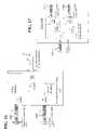
- Each network processor 106 A, 106 Bis also coupled to the packet bus 126 A, 126 C via the output busses 254 A, 254 B and the packet bus interface 128 A, 128 B for transmitting packet data to the corresponding secondary processing element 112 A, 1112 B.
- the output busses 254 A, 254 Bare each 32 bits wide and operate at 84 MHz, complying with the IX bus protocol and operating in a master/slave unidirectional configuration.
- the packet bus interface 128 A, 128 Bcouples the two 32 bit busses from the network processors 106 A, 106 B with the packet bus 126 A, 126 C.
- the packet bus 126 A, 126 Cis 64 bits wide and operates at a frequency of at least 84 MHz and complies with IX bus protocol operating in a bi-directional configuration, as described above.
- the packet bus interface 128 A, 128 Bconverts between the 32 and 64 bit bus widths.
- the packet bus interfaceis implemented as an field programmable gate array (“FPGA”).
- FIG. 17shows a detailed diagram of an exemplary packet bus interface 128 A, 128 B.
- the network processors 106 A, 106 Bare Intel IXP1200 network processors, described above, which provide a 64 bit IX bus interface configurable as two 32 bit unidirectional interfaces.
- the input busses 208 A, 208 Bare coupled with one half (32 bits) of the IX bus interface of each network processor 106 A, 106 B.
- the output busses 254 A, 254 Bare coupled with the other half (32 bits) of the IX bus interface of each network processor 106 A, 106 B. It will be appreciated that the input/output interfaces and bus protocols are processor architecture dependent and vary among manufacturers.
- the packet busses 126 A, 126 B, 126 C, 126 Dalso use the IX bus of the network processors 106 A, 106 B.
- Each network processor 106 A, 106 Bis coupled with a command/control bus interface 116 A, 116 B via command/control interface busses 130 A, 130 B which interfaces the network processors 106 A, 106 B to the command/control bus 124 .
- the command/control interface busses 130 A, 130 Bare 32 bit wide PCI compliant busses operating at 33 MHz.
- the command/control bus interfaces 116 A, 116 Bcomprise PCI to cPCI bridge interfaces 116 A, 116 B which interfaces the network processor 106 A, 106 B to a cPCI bus 124 .
- the cPCI bus 124interconnects the primary processing element 104 A, 104 B with other processing elements 104 and other resources (not shown) of the device 100 allowing the sharing of data and distribution of packet processing, as described above.
- the PCI to cPCI bridge interface 116 A, 116 Bincludes model I21154, manufactured by Intel Corporation, located in Santa Clara, Calif. Alternatively, other bus architectures may be used for communication among the components of the device 100 .
- Each network processor 106 A, 106 Bis further coupled with a bank 210 A, 210 B of sync burst static random access memory (“SSRAM”) via an SSRAM data interface 212 A, 212 B and an SSRAM address interface 214 A, 214 B provided by the network processor 106 A, 106 B.
- SSRAM data and address interfaces 212 A, 212 B, 214 A, 214 Bare 32 bits wide and operate at a frequency of at least 100 MHz.
- Each bank 210 A, 210 B of SSRAMincludes a block 218 A, 218 B of one or more single port SSRAM devices and a block 216 A, 216 B of one or more dual port SSRAM (“DPSSRAM”) devices.
- DPSSRAMdual port SSRAM
- the combined blocks 216 A, 218 A and 216 B, 218 B for each network processor 106 A, 106 Bare configured as a contiguous address space to the network processor 106 A, 106 B, described in more detail below.
- the single port SSRAM devicesinclude MT48LC32M8A2FC-75, manufactured by Micron Technologies, Inc, located in Boise, Id. and the dual port DPSSRAM devices include 16 K ⁇ 36 synchronous pipelined dual port SRAM's IDT70V3569, manufactured by IDT, Inc., located in Santa Clara, Calif.
- the network processors 106 A, 106 Bare coupled with one of the two ports of their respective DPSSRAM blocks 216 A, 216 B.
- Each network processor 106 A, 106 Bis further coupled with SRAM control logic 228 A, 228 B, also known as the address decode filter (“ADF”) FPGA, via the SRAM control logic address interface 230 A, 230 B.
- SRAM control logic 228 A, 228 B (ADF) 228 A, 228 Bis coupled with and snoops/listens in on the SRAM control logic address interface 230 A, 230 B of the corresponding DPSSRAM block 216 A, 216 B and captures any transmitted address if it falls into the co-processors 108 operational command/data address range.
- the SRAM control logic 228 A, 228 Bfilters the address from the network processors 106 C and 106 D by SRAM control logic address interface 230 A, 230 B and on a match for a co-processor operation by the network processor, 106 C, 106 D, the address sent by network processor, 106 C, 106 D to the SSRAM 210 A, 210 B is captured and placed in an internal first in first out (“FIFO”) queue of the SRAM control logic 228 A, 228 B which is than passed to daughter card control logic 236 .
- FIFOfirst in first out
- the DPSSRAM blocks 216 A, 216 Bare also coupled with the daughter card 204 via the DPSSRAM daughter card interfaces 232 A, 232 B.
- the DPSSRAM daughter card interface 232 A, 232 Bare each at least 64 bits wide and operate at a frequency of at least 50 MHz.
- the SRAM control logic 228 A, 228 B. 328is coupled with the daughter card 204 via SRAM control logic daughter card interfaces 234 A, 234 B.
- the SRAM control logic 228 A, 228 B, 328is a custom designed device using a CMOS Programmable Logic Device (“CPLD”). Operation of the SRAM control logic 228 A, 228 , 328 is described in more detail below.
- CPLDCMOS Programmable Logic Device
- the primary processing element 104 A, 104 Bfurther includes a daughter card connector 246 for connecting an auxiliary printed circuit board, also known as a daughter card, 204 to the main circuit board 202 of the primary processing element 104 A, 104 B.
- the daughter card connector 246includes two 140 pin high density connectors, one to interface each network processor 106 A, 106 B.
- An exemplary high density connectoris the QStrip QTE/QSE series connector from Samtec, Inc. located in New Albany, Ind. Alternatively, other connector interfaces and protocols may be used.
- TDO MB to CC Boundary-scan Test-Access-Port output dataCPGM# MB to CC Configuration Programming. CINIT# MB to CC Configuration Init. CCLK MB to CC Configuration Clock. CDIN MB to CC Configuration data input to CC FPGA. CDONE CC to MB Configuration done.
- the daughter card 204includes daughter card control logic 236 and the co-processor 108 set 122 A, 122 B.
- the co-processor 108 set 122 A, 122 Bincludes two classification co-processors and eight content addressable memories (“CAM”) cascaded to supply CAM and classification banks.
- the daughter card control logic 236interfaces with the DPSSRAM daughter card interfaces 232 A, 232 B and the SRAM control logic daughter card interfaces 234 A, 234 B.
- the daughter card control logic 236is further coupled with each of the co-processors 108 via co-processor interfaces 238 .
- Each co-processormay further be coupled with each other in a cascaded fashion via a inter-co-processor interface bus (not shown). It will be appreciated that other components located on the main circuit board 202 can be moved to the daughter card 204 and vice versa depending on the implementation of the processing element 104 and the desired performance requirements.
- both network processors 106 A, 106 Bshare the same set 122 A, 122 B of co-processors 108 .
- the daughter card control logic 236interfaces all of the co-processors 108 to the network processors 106 A, 106 B as will be described below.
- each network processor 106 A, 106 Bmay have its own set 122 A, 122 B of co-processors 108 .
- the primary processing element 104 A, 104 Bmay include two daughter cards 204 , one for each network processor 106 A, 106 B.
- eachmay have its own daughter card including the set 122 C of co-processors.
- FIG. 4shows a more detailed schematic diagram of the primary processing element 104 A, 104 B.
- FIG. 5shows a more detailed schematic diagram of the interconnections of one of the network processors 106 A, 106 B with the daughter card control logic 236 .
- FIG. 6shows a more detailed diagram of the interfaces of the SRAM control logic 228 A, 228 B.
- the following tableexplains the signal names used in FIG. 6 :
- REN# I FIFO read enableAsserted by the CAM/Classify FPGA. RCLK I FIFO read clock. Generated by the CAM/Classify FPGA. FF# O FIFO full flag. EF# O FIFO empty flag. GCK0, GCK1, I Clock inputs for Global Clock Buffers. GCK2, GCK3 M0, M1, M2 I Mode pins. Specify the configuration mode. CCLK I/O Configuration clock I/O pin. Input for SelectRAM and slave-serial modes. Output in master-slave mode.
- DONE I/OIndicates that the configuration loading is complete, and that the start-up sequence is in progress.
- the outputmay be open drain.
- Output Lowto indicate that the configuration memory is being cleared.
- the pinbecomes user I/O after configuration.
- DOUT/BUSY O Configuration data output pinThe pin becomes user I/O after configuration. DIN/D0, D1, D2, I Configuration data input pin. The pin becomes user D3, D4, D5, D6, D7 I/O after configuration.
- FIG. 7shows a more detailed diagram of the interfaces 212 A, 212 B, 214 A, 214 B, 232 A, 232 B to the DPSSRAM 216 A, 216 B and how the DPSSRAM memory devices are interleaved, described in more detail below.
- FIGS. 8 and 9show more detailed schematic diagrams of the daughter card 204 and the interfaces to the daughter card control logic 236 .
- FIGS. 8 and 9further show the cascaded interconnections between the co-processors 108 and the daughter card control logic 236 .
- the CAM co-processors 108provide a bi-directional 36/72 bit comparand bus (“cBus”) for a 1 megabit part and a 72/144 bit bus for a 9 megabit part. This allows access to all of the internal registers and memory of the CAM co-processor 108 .
- the CAM co-processors 108further provide a 32 bit result bus (“rBus”) which provides the result after completion of a compare operation.
- the CAM co-processors 108provide a 16 bit instruction bus (“iBus”) that allows instructions to be presented to the device once every cycle.
- the CAM co-processors 108provide an output only 24 bit Next Free Address (“NFA”) bus that provides the next free address available.
- the flag I/O bitspermit search depth cascading, as described above, without the need for glue logic.
- the network processor 106 A, 106 B to co-processor 108 interfaceis separated by the DPSSRAM 216 A, 216 B.
- the DPSSRAM 216 A, 216 Beffectively acts as fast a bi-directional message passing buffer between the network processors 106 A, 106 B and the co-processors 108 .
- Dual ported memoriesand in particular, DPSSRAM's, are designed to allow two separate and independent devices to access the memory at any given time, asynchronously.
- An exemplary use of dual ported memoryis in computer video memory where the video data is written through one port by the computer and read out through the second port by video driver.
- the two interfaces of the DPSSRAM 216 A, 216 Bare independently driven and isolated by the memory.
- the network processors 106 A, 106 Btherefore need only contend with making data read and write operations to the DPSSRAM 216 A, 216 B which makes co-processor 108 operations transparent to the network processors 106 A, 106 B and asynchronous to the system clock. Further, this design lowers complexity and development cycle risks.
- each SSRAM bank 210 A, 210 Bincludes a block of normal SSRAM 218 A, 218 B and a block of interleaved DPSSRAM 216 A, 216 B.
- the SSRAM bank 210 A, 210 B address spaceis arranged such that the DPSSRAM 216 A, 216 B devices occupy the upper portion of the address space.
- network processors 106 A, 106 Bcan address up to 8 megabytes of SSRAM memory.
- the SSRAM bank 210 A, 210 Bincludes three 16 megabit (2 megabyte) SSRAM devices, each having a 32 bit ⁇ 512 K row organization, and two 0.5 megabit DPSSRAM devices, each having a 36 bit ⁇ 16 K row organization, occupying 32 kilo-double words of the remaining 2 megabyte address space. Further, the two DPSSRAM devices are interleaved on even and odd double word boundaries.
- the network processors' 106 A, 106 B access to the memoriescan be operated at a nominal data rate and not effected by secondary bus speed.
- the network processors 106 A, 106 Bcan transfer their 32 bit data stream to the daughter card control logic 236 at a processing rate of at least 100 MHz.
- the network processorscan still move a 32 bit transfer stream at normal rates to both the SSRAM block 218 A, 218 B and the DPSSRAM block 216 A, 216 B.
- the SSRAM bank 210 A, 210 Bmay include more or less memory and may utilize memory devices having alternate array organizations.
- FIG. 11shows a memory map 1200 of the DPSSRAM 216 A, 216 B. Further, this Figure shows how the memory is mapped for communications between the network processors 106 A, 106 B and the CAM co-processors 108 . It will be appreciated that the memory map (not shown) of the DPSSRAM 216 A, 216 B for access by the network processors 106 A, 106 B to the classification co-processors 108 is similar to the map shown in FIG. 11 for the CAM co-processors 108 .
- the DPSSRAM 216 A, 216 Bis divided into section 1202 , 1204 , 1206 , 1208 .
- These sections 1202 , 1204 , 1206 , 1208are used for facilitating communications between the network processors 106 A, 106 B and the CAM co-processors 108 .
- the CAM co-processor 108 memory sections 1202 , 1204 , 1206 , 1208are each 24 double words. It will be appreciated that the amount of memory, and structure of that memory is implementation dependent and that other organizations or different size memories may be used. The organization and function of these memory sections is described in more detail below.
- the memory map 1200details how the DPSSRAM memory 216 A, 216 B is utilized to transfer data between the network processor 106 A, 106 B and the CAM co-processors 108 .
- the network processor 106 A, 106 B side of the DPSSRAM 216 A, 216 Bis connected directly to the network processor 106 A, 106 B processor.
- the co-processor 108 side of the DPSSRAM 216 A, 216 Bis connected to the daughter card control logic 236 that controls data transfers between the DPSSRAM 216 A, 216 B and the CAM co-processors 108 .
- the DPSSRAM 216 A, 216 Bis divided into 4 segments 1202 , 1204 , 1206 , 1208 .
- Each segment 1202 , 1204 , 1206 , 1208is directly related to the CAM's 108 comparand word length of 36–288 bits long in increments of a quad-word to address bits 0 – 288 in steps.
- segment 0 1202allows any of the six network processor 106 A, 106 B micro-engines and the associated 4 threads 1212 per micro-engine to access the CAM's 108 comparand word [0–71].
- Segment 1 1204transfers data between the network processor's 106 A, 106 B micro-engines and the CAM's 108 comparand data register bits [72:135] by setting the CAM word control signals to LWEN[0:1].
- Segments 3 & 4 1206 , 1208transfer the network processor's 106 A, 106 B data to the CAM's 108 register bits 136 – 288 , corresponding to LWEN [1:0] & LWEN [1:1] respectively.
- Each segment 1202 , 1204 , 1206 , 1208is therefore subdivided into six access spaces 1210 , one for each micro-engine of the network processor 106 A, 106 B. Further, each access space 1210 is sub-divided into four threads 1212 for each of the processing threads that the six micro-engines of the exemplary network processors 106 A, 106 B are capable of executing.
- This formatallows very efficient Quad word data transfers between the respective processing threads of the network processor's 106 A, 106 B micro-engines and the CAM co-processors 108 . The data transfers from the threads remain independent from each other for both read and writes.
- Write operations by network processors 106 A, 106 Boccur simply by the thread of a micro-engine writing a data word to the appropriate segment of the DPSSRAM 216 A, 216 B corresponding to the word in the CAM's 108 0–288 bit registers. Read operations are similar to the writes but due to the pipeline between the two interleaved DPSSRAM devices and the CAM co-processor 108 through the control logic 236 , the reads are delayed reads.
- the network processor 106 A, 106 Bwrites the read instruction as a double word or quad Word and some cycles later, on the order of 200–300 microseconds, it will read the result back from the DPSSRAM memory segment where the tread had written the read command.
- Each quad data word areais used to support all the command variances as well for all data transfers.
- the lower double word from the network processor 106 A, 106 B to CAM co-processor 108contains 16 bit CAM op-code together with several control bits that the daughter card control logic 236 uses to supply network processor 106 A, 106 B with CAM 108 results or the next free address (“NFA”) in the CAM co-processor 108 table entry and respective flag status.
- FIG. 11further shows this command format 1212 .
- Exemplary CAM co-processor 108 instructionsare detailed in Appendix A.
- FIG. 12shows a memory map 1300 of the network processor 106 A, 106 B to classification co-processors 108 data transfer section 1102 of the DPSSRAM 216 A, 216 B.
- the classification co-processors 108support 32 independent processing channels allowing 32 independent contexts to use the classification co-processors 108 without the need of any semaphore protocol among the contexts.
- the first 16 channelsare allocated to one network processor 106 A, 106 B and the other 16 channels are allowed to the other network processor 106 A, 106 B on the primary processing element 104 A, 104 B.
- each channelcan process packets with a maximum length of 256 bytes, however segments may be concatenated together to allow for longer packets.
- FIG. 13shows a memory map 1400 for the local register pointers. Showing how the various micro-engines of the network processors 106 A, 106 B and the respective thread of the network processor 106 A, 106 B can cleanly access the classification co-processor 108 local registers with a command block structure of register address, command/data and semaphore flag to indicate direction of the data between the network processor 106 A, 106 B and the classification co-processor 108 .
- FIG. 14shows a memory map 1500 for the packet input buffer of the co-processor 108 and the respective 32 channels that the network processor 106 A, 106 B can access via the DPSSRAM 216 A, 216 B mapped space.
- the classification co-processor 108supports local as well global registers and buffers.
- the DPSSRAM 216 A, 216 Bthe network processor 106 A, 106 B to address all the classification co-processor 108 resources as needed by each network processor 106 A, 106 B and the threads per processor.
- FIGS. 13 and 14show the mapping of all the classification co-processor 108 resources available to the network processor 106 A, 106 B.
- the network processor 106 A, 106 Bwill configure the classification co-processor 108 at power up. Further set-up the rule memory through indirect address rule memory buffers in the classification co-processor 108 .
- the classification co-processor 108is configured and loaded with the search tree rules, the data to be processed is written to the classification co-processor 108 by the network processor 106 A, 106 B by loading each of the 32 channels of 108 . Each channel can be up to 255 bytes with the 256 double words being the indication to start the computation.
- the classification co-processor 108indicates the completion of the channel operation by the channel completion number and flags. At that point the result of the operation is available in the result memory space 0 and 1.
- One method for reading the result back by the network processor 106 A, 106 Bis to react to the channel ready hard ware signs or interrupt from the classification co-processor 108 .
- DPSSRAM 216 A, 216 B and the daughter card control logic 236it becomes feasible to read the classification co-processor 108 results on completion and write then back to the respective channel mapped into the DPSSRAM 216 A, 216 B.
- the network processor 106 A, 106 Bperiodically will read the semaphore flag in the DPSSRAM 216 A, 216 B for the corresponding channel and if the direction flag is active, the network processor 106 A, 106 B can read the respective channel data back.
- the mechanism supported by the DPSSRAM 216 A, 216 B, SRAM control logic 228 A, 228 B, and the daughter card control logic 236allows smooth operation with out network processor 106 A, 106 B having to wait on tasks pending.
- the architecturealso allows multiple threads to operate independently in parallel thus improving the network processor 106 A, 106 B performance by many times than had it been connected directly to the classification co-processor 108 .
- One other issue with using the DPSSRAM 216 A, 216 B in this applicationis that the network processor 106 A, 106 B writes to memory is not reflected on the secondary side of the device. In other words, the co-processors 108 do not know when the network processor 106 A, 106 B writes data to the DPSSRAM 216 A, 216 B and vice versa.
- One alternativeis to use semaphores, i.e. flags written to the DPSSRAM 216 A, 216 B which are continuously polled by the network processor 106 A, 106 B and the co-processors 108 , for data transfers between the two sides of the memory.
- semaphoresi.e. flags written to the DPSSRAM 216 A, 216 B which are continuously polled by the network processor 106 A, 106 B and the co-processors 108 , for data transfers between the two sides of the memory.
- thisis impractical here given that the network processor 106 A, 106 B has six micro
- custom SRAM control logic 228 A, 228 Bis implemented using a field programmable gate array (“FPGA”) that snoops on the network processor 106 A, 106 B address bus 214 A, 214 B for DPSSRAM 216 A, 216 B read/writes.
- FPGAfield programmable gate array
- the custom SRAM control logic 228 A, 228 Bis also referred to as the Address Filter FPGA (“ADF FPGA”).
- ADF FPGAAddress Filter FPGA
- all of the co-processors 108are coupled with the daughter card control logic 236 which mediates communications between the co-processors 108 and the DPSSRAM 216 A, 216 B, described in more detail below.
- the network processor 106 A, 106 B operationsare reported to the daughter card control logic 236 by the SRAM control logic.
- the SRAM control logicBy memory mapping the DPSSRAM 216 A, 216 B, as described above, in such way that network processor 106 A, 106 B writes to a particular segment of the memory triggers a known SRAM control logic 228 A, 228 B task, the data transfers between the network processor 106 A, 106 B and the co-processors 108 can be effected via the DPSSRAM 216 A, 216 B.
- a first-in-first-out queuemay be used that captures the network processor 106 A, 106 B transfers in the address pace of the DPSSRAM 216 A, 216 B.
- the daughter card control logic 236can then retrieve the address from the FIFO queue and retrieve the respective data from the DPSSRAM 216 A, 216 B.
- Operation of the SRAM control logic 228 A, 228 Bis similar to the FIFO, however the SRAM control logic 228 A, 228 B is able to do address decoding internally before signaling the daughter card control logic 236 on the daughter card 204 .
- the DPSSRAM 216 A, 216 Bis mapped such that the network processors 106 A, 106 B can address all of the co-processors 108 as though they were connected directly to its SRAM bus 212 A, 212 B, 214 A, 214 B.
- the DPSSRAM 216 A, 216 B address on the both sideshave no correlation to the operations occurring on either side. This imposes some changes in how the network processor 106 A, 106 B conducts read and write operations.
- the network processor 106 A, 106 Bmust initiate a dummy read and then wait for the daughter card control logic 236 to retrieve the data and write it to the DPSSRAM 216 A, 216 B some specified cycles later. The network processor 106 A, 106 B then reads the actual data from the desired location.
- the network processor 106 A, 106 BIn actual fact, for the network processor 106 A, 106 B to read co-processor 108 data is not a problem.
- the co-processorexpects a command even for data read. This implies that the network processor 106 A, 106 B must send (write) a command to the DPSSRAM 216 A, 216 B segment 802 , 804 , 806 , 808 .
- the daughter card control logic 236retrieves the op-code written by the network processor 106 A, 106 B and decodes it to see if it is a write or read data operation being requested.
- the op-code most significant bits (“MSB”) bitsindicate the operation being requested.
- MSBmost significant bits
- a read commandFor a read command, it reads the data from the CAM co-processor 108 RBUS after compare command or data bus (CBUS) and delivers it to the DPSSRAM 216 A, 216 B segment 802 , 804 , 806 , 808 where the command was issued from.
- CBUScompare command or data bus
- NFAnext free address
- a single bit tokenis exchanged from the segment 802 , 804 , 806 , 808 between the network processor 106 A, 106 B and the daughter card control logic 236 .
- the daughter card control logic 236captures the appropriate NFA data together with the co-processor 108 flags and writes the data back at the DPSSRAM 216 A, 216 B.
- the network processor 106 A, 106 Bpolls the MSB, D[15] of the least significant double word and retrieves the data on the bit set active high.
- the SRAM control logic 228 A, 228 Bmonitors the traffic over the network processor 106 A, 106 B SRAM Interface 212 A, 212 B, 214 A, 214 B to the DPSSRAM 216 A, 216 B and manages the data transfer to the daughter card control logic 236 on the daughter board 204 .
- the DPSSRAMcannot convey the address between the two sides of the memory as they independently operate on the common storage cells.
- This designwould have created problems as the daughter card control logic 236 managing the co-processors 108 needs to know when even the network processor 106 A, 106 B writes a command to the DPSSRAM 216 A, 216 B.
- the SRAM control logic 228 A, 228 Bthus serves as the address decoder and informs the daughter card control logic 236 of any writes to the DPSSRAM 216 A, 216 B and the address to which the write occurred. This information is than used by the daughter card control logic 236 to prompt the appropriate one of the following actions:
- the main function of the SRAM control logic 228 A, 228 Bis to snoop the network processor SRAM address bus 214 A, 214 B together with the control signals and map the DPSSRAM 216 A, 216 B read/write operations into the top 32 K or 64 K portion of the 8 megabyte SRAM address spaces of the network processor 106 A, 106 B, as described above.
- the writes from the network processor 106 A, 106 Bgo to both the DPSSRAM 216 A, 216 B as well as the corresponding address within the 8 megabytes of main SSRAM.
- the network processor 106 A, 106 Bcan be loaded with 2, 4, or 6 megabytes of SSRAM in which case the DPSSRAM 216 A, 216 B occupies the top 32 k/64 K ⁇ 32 bit of the top 2 megabytes of the SSRAM memory map.
- the memory map shown in FIG. 11assumes that only 6 megabytes of SSRAM are attached to each of the two network processors 106 A, 106 B and the DPSSRAM 216 A, 216 B is mapped into the top 2 megabytes of SSRAM space. If the 4th SSRAM was to be included, the read operations to the shared space of the main SSRAM can be avoided by controlling the output enable of the SSRAM devices which implement the top of the address space from the SRAM control logic 228 A, 228 B.
- Each DPSSRAM 216 A, 216 B memoryis mapped into the 8 megabyte SRAM address spaces of the corresponding network processors 106 A, 106 B on the processing element 104 .
- DPSSRAM 216 A, 216 Bare typically available in 16–256 K ⁇ 32 bit capacity.
- the DPSSRAM 216 A, 216 Bis further partitioned into blocks corresponding to the CAM or classification co-processors 108 .
- FIG. 15shows a block diagram 1000 of the daughter card control logic 236 . It shows the command, data and bi-directional paths and the arbitration between the two network processors 106 A, 106 B to access the co-processors 108 .
- the network processors 106 A, 106 Bare coupled to one port of the DPSSRAM 216 A, 216 B via the SRAM memory data and address busses 212 A, 214 A.
- the SRAM control logic 228 A, 228 Bsnoops the SRAM memory address bus 214 A via bus 230 A and watches for co-processor 108 operations written by the network processors 106 A, 106 B.
- the SRAM control logic 228 A, 228 Binforms the daughter card control logic 236 .
- the daughter card control logic 236reads the address of the DPSSRAM 216 A, 216 B that the network processor 106 A, 106 B had written the command to.
- the daughter card control logic 236then reads the DPSSRAM 216 A, 216 B location using the address from the SRAM control logic 228 A, 228 B and loads it in internal buffers.
- the daughter card control logicthen checks the type of operation and passes the command/data to the respective co-processor's 108 first-in-first-out (“FIFO”) queue. On availability of the co-processor's 108 interface, the FIFO data and the commands are passed on together with the address to that co-processor 108 . The co-processor uses the data to start the process and at a later time generates the result. Based on the result flags, the daughter card control logic 236 moves the data back to the DPSSRAM 216 A, 216 B of the appropriate network processor 106 A, 106 B and writes the result together with the semaphore flag indicating to the network processor 106 A, 106 B that the data is valid.
- FIFOfirst-in-first-out
- the CAM co-processors 108are capable of being cascaded together. For cascading anywhere from 2–8 CAM co-processors 108 , the match I/O signals and all of the flag signals of each CAM co-processor 108 need to be connected from co-processor 108 to co-processor.
- the co-processor 108 which represents the least significant bitsserves as inputs and the co-processor 108 which represents the most significant bits serves as the output to the daughter card control logic 236 .
- the order of the CAM co-processors 108must be configured via configuration registers within each CAM co-processor 108 . For write operations to the appropriate CAM co-processor 108 , the daughter card control logic 236 must enable the corresponding CAM co-processor 108 chip enable pin (“/CE”).
- FIG. 9shows the block diagram of a portion of the daughter card control logic 236 interface related to interfacing with cascaded CAM co-processors 108 .
- the data input of the daughter card control logic 236is coupled with the DPSSRAM 216 A, 216 B and the control signal inputs are coupled with the SRAM control logic 228 A, 228 B on the main circuit board 202 of the processing element 104 via the connector 246 .
- the daughter card control logic 236supports access by two network processors 106 A, 106 B, as described, to the common CAM co-processors 108 in the cascaded configuration. Since each micro engine works on the quad word boundaries, the data transfers from the DPSSRAM 216 A, 216 B to daughter card control logic 236 are quad word based data transfers. To further improve the network processor 106 A, 106 B micro-engines performance, the daughter card control logic 236 needs to provide a mechanism where by the data flow between the CAM co-processors 108 and the network processor 106 A, 106 B can be packed and unpacked.
Landscapes
- Engineering & Computer Science (AREA)
- Theoretical Computer Science (AREA)
- Software Systems (AREA)
- Physics & Mathematics (AREA)
- General Engineering & Computer Science (AREA)
- General Physics & Mathematics (AREA)
- Computer Hardware Design (AREA)
- Data Exchanges In Wide-Area Networks (AREA)
Abstract
Description
- Organization options of any single device in cascade: 64 K×72, 32 K×144 or 16 K×288;
- Local mask bit associated with each CAM;
- Clock rates: 50/66/100 MHz for 1 megabit devices or up to 200 MHz for a 9 megabit device;
- Eight global mask registers;
- 16 bit instruction bus;
- 32 bit result bus;
- 36/72 bit comparand bi-directional bus or 72/144 bit comparand bus for a 9 megabit device;
- flags to indicate Match (“/M”), Multiple Match (“/MM”) and Full Flag (“/FF”); and
- 24 bit Next Free Address (“NFA”) bus.
| SYMBOL | Direction | DESCRIPTION |
| GND | MB to CC | Ground |
| RST# | MB to CC | Chip reset. |
| MCLK | MB to CC | Chip Master clock. |
| DP_A(1) | CC to MB | Dual-Port SRAM address. |
| DP_A(2) | CC to MB | Dual-Port SRAM address. |
| DP_A(3) | CC to MB | Dual-Port SRAM address. |
| DP_A(4) | CC to MB | Dual-Port SRAM address. |
| DP_A(5) | CC to MB | Dual-Port SRAM address. |
| DP_A(6) | CC to MB | Dual-Port SRAM address. |
| DP_A(7) | CC to MB | Dual-Port SRAM address. |
| DP_A(8) | CC to MB | Dual-Port SRAM address. |
| DP_A(9) | CC to MB | Dual-Port SRAM address. |
| DP_A(10) | CC to MB | Dual-Port SRAM address. |
| DP_A(11) | CC to MB | Dual-Port SRAM address. |
| DP_A(12) | CC to MB | Dual-Port SRAM address. |
| DP_A(13) | CC to MB | Dual-Port SRAM address. |
| DP_A(14) | CC to MB | Dual-Port SRAM address. |
| DP_WE# | CC to MB | Dual-Port SRAM write enable. |
| DP_CE# | CC to MB | Dual-Port SRAM chip enable. |
| DP_CLK | CC to MB | Dual-Port SRAM clock. |
| DP_D(63:0) | Bi-direction | Dual-Port SRAM data. |
| AFC_D(63:0) | MB to CC | Address Filter Chip data. |
| AFC_RD# | CC to MB | Address Filter Chip read enable. |
| AFC_CLK | CC to MB | Address Filter Chip read clock. |
| AFC_FFSEL | CC to MB | Address Filter Chip FIFO select.0: |
| CAM FIFO1: Classify FIFO | ||
| AFC_FF# | MB to CC | Address Filter Chip Full Flag. |
| AFC_EF# | MB to CC | Address Filter Chip Empty Flag. |
| TCK | MB to CC | Boundary-scan Test-Access-Port clock. |
| TMS | MB to CC | Boundary-scan Test-Access-Port mode |
| select. | ||
| TDI | MB to CC | Boundary-scan Test-Access-Port input |
| data. | ||
| TDO | MB to CC | Boundary-scan Test-Access-Port output |
| data. | ||
| CPGM# | MB to CC | Configuration Programming. |
| CINIT# | MB to CC | Configuration Init. |
| CCLK | MB to CC | Configuration Clock. |
| CDIN | MB to CC | Configuration data input to CC FPGA. |
| CDONE | CC to MB | Configuration done. |
| SYMBOL | I/O | DESCRIPTION |
| RST# | I | Chip reset. |
| FFSEL | I | FIFO select.0: CAM FIFO1: Classify FIFO |
| DIN(15:0) | I | FIFO data inputs. Connect the IXP's SRAM |
| interface A(14:1) to DIN(13:0). Pin DIN(15:14) are | ||
| spare. | ||
| WEN# | I | FIFO write enable. Indicates the IXP is writing to the |
| Dual Port SRAM. | ||
| CEN# | I | FIFO chip enable. Indicates the IXP is accessing the |
| Dual Port SRAM. | ||
| WCLK | I | FIFO write clock. Connect to the IXP SCLK, which |
| is 1/2 the rate of the IXP core clock. | ||
| DOUT(15:0) | O | FIFO data outputs. Correlates to the address that the |
| processor is writing to the Dual Port SRAM. Only | ||
| bits DOUT(13:0) are defined. The DOUT(15:14) are | ||
| spare. | ||
| REN# | I | FIFO read enable. Asserted by the CAM/Classify |
| FPGA. | ||
| RCLK | I | FIFO read clock. Generated by the CAM/Classify |
| FPGA. | ||
| FF# | O | FIFO full flag. |
| EF# | O | FIFO empty flag. |
| GCK0, GCK1, | I | Clock inputs for Global Clock Buffers. |
| GCK2, GCK3 | ||
| M0, M1, M2 | I | Mode pins. Specify the configuration mode. |
| CCLK | I/O | Configuration clock I/O pin. Input for SelectRAM |
| and slave-serial modes. Output in master-slave | ||
| mode. | ||
| PROGRAM# | I | Asserted low to initiate a configuration sequence. |
| DONE | I/O | Indicates that the configuration loading is complete, |
| and that the start-up sequence is in progress. The | ||
| output may be open drain. | ||
| INIT# | I/O | Open-drain. Output Low to indicate that the |
| configuration memory is being cleared. The pin | ||
| becomes user I/O after configuration. | ||
| DOUT/BUSY | O | Configuration data output pin. The pin becomes user |
| I/O after configuration. | ||
| DIN/D0, D1, D2, | I | Configuration data input pin. The pin becomes user |
| D3, D4, D5, D6, D7 | I/O after configuration. | |
| WRITE# | I | Configuration pin for Slave Parallel mode. |
| CS# | I | Configuration pin for Slave Parallel mode. |
| TDI, TMS, TCK | I | Boundary-scan Test-Access-Port input pin. |
| TDO | O | Boundary-scan Test-Access-Port output pin. |
| VCCO | I | Power supply pin for output drivers. |
| VCCINT | I | Power supply pin for internal core logic. |
| GND | I | Ground |
| VREF | I | Input threshold voltage pin. |
| PWDN# | I | Logic high for normal operation. Logic low for |
| power down mode. | ||
| STATUS | O | Logic low when the part is in power down mode. |
| Logic high when the part is ready to resume normal | ||
| operation. | ||
- Co-processor108 maintenance (Read/write to control registers or read status);
- Execute co-processor108 operation on the data in
DPSSRAM CAM co-processor 108 or a classification operation in theclassification co-processor 108; - Daughter
card control logic 236 register update (FPA functionality); and - Transfer data to
secondary network processor network processors
Claims (42)
Priority Applications (2)
| Application Number | Priority Date | Filing Date | Title |
|---|---|---|---|
| US09/858,308US7210022B2 (en) | 2001-05-15 | 2001-05-15 | Apparatus and method for interconnecting a processor to co-processors using a shared memory as the communication interface |
| US11/182,141US7318144B2 (en) | 2001-05-15 | 2005-07-15 | Apparatus and method for interconnecting a processor to co-processors using shared memory |
Applications Claiming Priority (1)
| Application Number | Priority Date | Filing Date | Title |
|---|---|---|---|
| US09/858,308US7210022B2 (en) | 2001-05-15 | 2001-05-15 | Apparatus and method for interconnecting a processor to co-processors using a shared memory as the communication interface |
Related Child Applications (1)
| Application Number | Title | Priority Date | Filing Date |
|---|---|---|---|
| US11/182,141ContinuationUS7318144B2 (en) | 2001-05-15 | 2005-07-15 | Apparatus and method for interconnecting a processor to co-processors using shared memory |
Publications (2)
| Publication Number | Publication Date |
|---|---|
| US20030009651A1 US20030009651A1 (en) | 2003-01-09 |
| US7210022B2true US7210022B2 (en) | 2007-04-24 |
Family
ID=25327989
Family Applications (2)
| Application Number | Title | Priority Date | Filing Date |
|---|---|---|---|
| US09/858,308Expired - LifetimeUS7210022B2 (en) | 2001-05-15 | 2001-05-15 | Apparatus and method for interconnecting a processor to co-processors using a shared memory as the communication interface |
| US11/182,141Expired - LifetimeUS7318144B2 (en) | 2001-05-15 | 2005-07-15 | Apparatus and method for interconnecting a processor to co-processors using shared memory |
Family Applications After (1)
| Application Number | Title | Priority Date | Filing Date |
|---|---|---|---|
| US11/182,141Expired - LifetimeUS7318144B2 (en) | 2001-05-15 | 2005-07-15 | Apparatus and method for interconnecting a processor to co-processors using shared memory |
Country Status (1)
| Country | Link |
|---|---|
| US (2) | US7210022B2 (en) |
Cited By (12)
| Publication number | Priority date | Publication date | Assignee | Title |
|---|---|---|---|---|
| US20030202470A1 (en)* | 2002-04-25 | 2003-10-30 | Szumilas Lech J. | Method and apparatus for managing network traffic |
| US20050125784A1 (en)* | 2003-11-13 | 2005-06-09 | Rhode Island Board Of Governors For Higher Education | Hardware environment for low-overhead profiling |
| US20060004912A1 (en)* | 2001-05-15 | 2006-01-05 | Zahid Najam | Apparatus and method for interfacing with a high speed bi-directional network |
| US20060168283A1 (en)* | 2001-10-05 | 2006-07-27 | Georgiou Christos J | Programmable network protocol handler architecture |
| US20060179204A1 (en)* | 2005-02-08 | 2006-08-10 | Cohen Earl T | Method and apparatus for communicating over a resource interconnect |
| US20070288931A1 (en)* | 2006-05-25 | 2007-12-13 | Portal Player, Inc. | Multi processor and multi thread safe message queue with hardware assistance |
| US20080028186A1 (en)* | 2006-07-28 | 2008-01-31 | Drc Computer Corporation | FPGA Co-Processor For Accelerated Computation |
| US20080229157A1 (en)* | 2005-11-08 | 2008-09-18 | International Business Machines Corporation | Performing Externally Assisted Calls in a Heterogeneous Processing Complex |
| US20090086733A1 (en)* | 2004-03-29 | 2009-04-02 | Conexant Systems, Inc. | Compact Packet Switching Node Storage Architecture Employing Double Data Rate Synchronous Dynamic RAM |
| US7739426B1 (en) | 2005-10-31 | 2010-06-15 | Cisco Technology, Inc. | Descriptor transfer logic |
| US7934063B2 (en) | 2007-03-29 | 2011-04-26 | International Business Machines Corporation | Invoking externally assisted calls from an isolated environment |
| US8447957B1 (en)* | 2006-11-14 | 2013-05-21 | Xilinx, Inc. | Coprocessor interface architecture and methods of operating the same |
Families Citing this family (46)
| Publication number | Priority date | Publication date | Assignee | Title |
|---|---|---|---|---|
| US7032031B2 (en)* | 2000-06-23 | 2006-04-18 | Cloudshield Technologies, Inc. | Edge adapter apparatus and method |
| US7003555B1 (en)* | 2000-06-23 | 2006-02-21 | Cloudshield Technologies, Inc. | Apparatus and method for domain name resolution |
| US7114008B2 (en) | 2000-06-23 | 2006-09-26 | Cloudshield Technologies, Inc. | Edge adapter architecture apparatus and method |
| US9444785B2 (en) | 2000-06-23 | 2016-09-13 | Cloudshield Technologies, Inc. | Transparent provisioning of network access to an application |
| US8204082B2 (en) | 2000-06-23 | 2012-06-19 | Cloudshield Technologies, Inc. | Transparent provisioning of services over a network |
| US7233998B2 (en)* | 2001-03-22 | 2007-06-19 | Sony Computer Entertainment Inc. | Computer architecture and software cells for broadband networks |
| WO2003065177A2 (en)* | 2002-02-01 | 2003-08-07 | John Fairweather | System and method for navigating data |
| US7418574B2 (en)* | 2002-10-31 | 2008-08-26 | Lockheed Martin Corporation | Configuring a portion of a pipeline accelerator to generate pipeline date without a program instruction |
| US20050278503A1 (en)* | 2003-03-31 | 2005-12-15 | Mcdonnell Niall D | Coprocessor bus architecture |
| JP4224430B2 (en)* | 2003-07-07 | 2009-02-12 | 株式会社ルネサステクノロジ | Information processing device |
| US20050071828A1 (en)* | 2003-09-25 | 2005-03-31 | International Business Machines Corporation | System and method for compiling source code for multi-processor environments |
| US7475257B2 (en) | 2003-09-25 | 2009-01-06 | International Business Machines Corporation | System and method for selecting and using a signal processor in a multiprocessor system to operate as a security for encryption/decryption of data |
| US7523157B2 (en)* | 2003-09-25 | 2009-04-21 | International Business Machines Corporation | Managing a plurality of processors as devices |
| US7478390B2 (en)* | 2003-09-25 | 2009-01-13 | International Business Machines Corporation | Task queue management of virtual devices using a plurality of processors |
| US7146529B2 (en)* | 2003-09-25 | 2006-12-05 | International Business Machines Corporation | System and method for processor thread acting as a system service processor |
| US7549145B2 (en)* | 2003-09-25 | 2009-06-16 | International Business Machines Corporation | Processor dedicated code handling in a multi-processor environment |
| US7236998B2 (en)* | 2003-09-25 | 2007-06-26 | International Business Machines Corporation | System and method for solving a large system of dense linear equations |
| US20050071578A1 (en)* | 2003-09-25 | 2005-03-31 | International Business Machines Corporation | System and method for manipulating data with a plurality of processors |
| US7516456B2 (en)* | 2003-09-25 | 2009-04-07 | International Business Machines Corporation | Asymmetric heterogeneous multi-threaded operating system |
| US7444632B2 (en)* | 2003-09-25 | 2008-10-28 | International Business Machines Corporation | Balancing computational load across a plurality of processors |
| US7496917B2 (en)* | 2003-09-25 | 2009-02-24 | International Business Machines Corporation | Virtual devices using a pluarlity of processors |
| US7318218B2 (en)* | 2003-09-25 | 2008-01-08 | International Business Machines Corporation | System and method for processor thread for software debugging |
| US7415703B2 (en)* | 2003-09-25 | 2008-08-19 | International Business Machines Corporation | Loading software on a plurality of processors |
| US7389508B2 (en)* | 2003-09-25 | 2008-06-17 | International Business Machines Corporation | System and method for grouping processors and assigning shared memory space to a group in heterogeneous computer environment |
| US20050198482A1 (en)* | 2004-03-02 | 2005-09-08 | Altek Corporation | Central processing unit having a micro-code engine |
| US7200713B2 (en)* | 2004-03-29 | 2007-04-03 | Intel Corporation | Method of implementing off-chip cache memory in dual-use SRAM memory for network processors |
| US7962721B1 (en)* | 2004-05-04 | 2011-06-14 | Oracle America, Inc. | Method and apparatus for management of bus transactions relating to shared resources |
| US7676649B2 (en)* | 2004-10-01 | 2010-03-09 | Lockheed Martin Corporation | Computing machine with redundancy and related systems and methods |
| US7620042B2 (en)* | 2004-12-17 | 2009-11-17 | Samsung Electronics Co., Ltd. | Apparatus and method for inter-processor communications in a multiprocessor routing node |
| US7733857B2 (en)* | 2004-12-17 | 2010-06-08 | Samsung Electronics Co., Ltd. | Apparatus and method for sharing variables and resources in a multiprocessor routing node |
| US8279886B2 (en) | 2004-12-30 | 2012-10-02 | Intel Corporation | Dataport and methods thereof |
| US7743176B1 (en) | 2005-03-10 | 2010-06-22 | Xilinx, Inc. | Method and apparatus for communication between a processor and hardware blocks in a programmable logic device |
| US7669037B1 (en)* | 2005-03-10 | 2010-02-23 | Xilinx, Inc. | Method and apparatus for communication between a processor and hardware blocks in a programmable logic device |
| US7834658B1 (en)* | 2006-04-18 | 2010-11-16 | Xilinx, Inc. | Interface generation for coupling to a high-bandwidth interface |
| US8384700B2 (en) | 2007-01-26 | 2013-02-26 | Microsoft Corporation | Linked shell |
| WO2007138021A1 (en)* | 2006-05-29 | 2007-12-06 | Paschalis Papagrigoriou | Method for communication with a multi-function memory card |
| KR100781340B1 (en)* | 2006-09-18 | 2007-11-30 | 삼성전자주식회사 | Computation system and method for handling user-defined extended operations |
| US7925900B2 (en) | 2007-01-26 | 2011-04-12 | Microsoft Corporation | I/O co-processor coupled hybrid computing device |
| US7788470B1 (en)* | 2008-03-27 | 2010-08-31 | Xilinx, Inc. | Shadow pipeline in an auxiliary processor unit controller |
| US8060729B1 (en)* | 2008-10-03 | 2011-11-15 | Altera Corporation | Software based data flows addressing hardware block based processing requirements |
| EP2367117A1 (en)* | 2010-03-10 | 2011-09-21 | Panasonic Corporation | Heterogeneous routing network |
| US20110307847A1 (en)* | 2010-06-10 | 2011-12-15 | Global Unichip Corporation | Hybrid system combining TLM simulators and HW accelerators |
| US9129071B2 (en)* | 2012-10-24 | 2015-09-08 | Texas Instruments Incorporated | Coherence controller slot architecture allowing zero latency write commit |
| TWI480877B (en)* | 2013-11-11 | 2015-04-11 | Silicon Motion Inc | Storage unit and control system |
| US9460007B1 (en)* | 2014-09-24 | 2016-10-04 | Xilinx, Inc. | Programmable hardware blocks for time-sharing arithmetic units using memory mapping of periodic functions |
| TWI824318B (en)* | 2021-10-14 | 2023-12-01 | 欣興電子股份有限公司 | Circuit board connection structure |
Citations (48)
| Publication number | Priority date | Publication date | Assignee | Title |
|---|---|---|---|---|
| US4692918A (en) | 1984-12-17 | 1987-09-08 | At&T Bell Laboratories | Reliable local data network arrangement |
| US4744078A (en)* | 1985-05-13 | 1988-05-10 | Gould Inc. | Multiple path multiplexed host to network data communication system |
| US5195181A (en) | 1992-01-10 | 1993-03-16 | Digital Equipment Corporation | Message processing system having separate message receiving and transmitting processors with message processing being distributed between the separate processors |
| US5313586A (en)* | 1992-03-06 | 1994-05-17 | Intel Corporation | Co-processor de-coupling bus structure |
| US5406472A (en)* | 1991-12-06 | 1995-04-11 | Lucas Industries Plc | Multi-lane controller |
| US5566170A (en) | 1994-12-29 | 1996-10-15 | Storage Technology Corporation | Method and apparatus for accelerated packet forwarding |
| WO1998017039A1 (en) | 1996-10-14 | 1998-04-23 | Mirror Image Internet Ab | Internet communication system |
| US5784582A (en) | 1996-10-28 | 1998-07-21 | 3Com Corporation | Data processing system having memory controller for supplying current request and next request for access to the shared memory pipeline |
| US5805820A (en) | 1996-07-15 | 1998-09-08 | At&T Corp. | Method and apparatus for restricting access to private information in domain name systems by redirecting query requests |
| EP0865180A2 (en) | 1997-03-14 | 1998-09-16 | Lucent Technologies Inc. | Load distribution among servers in a TCP/IP network |
| US5822768A (en)* | 1996-01-11 | 1998-10-13 | Opti Inc. | Dual ported memory for a unified memory architecture |
| US5867704A (en) | 1995-02-24 | 1999-02-02 | Matsushita Electric Industrial Co., Ltd. | Multiprocessor system shaving processor based idle state detection and method of executing tasks in such a multiprocessor system |
| WO1999005584A2 (en) | 1997-07-24 | 1999-02-04 | Mirror Image Internet, Inc. | Internet caching system |
| US5870109A (en)* | 1997-06-06 | 1999-02-09 | Digital Equipment Corporation | Graphic system with read/write overlap detector |
| WO1999009725A1 (en) | 1997-08-21 | 1999-02-25 | At & T Corp. | Packet redirection and message stream management |
| WO1999027684A1 (en) | 1997-11-25 | 1999-06-03 | Packeteer, Inc. | Method for automatically classifying traffic in a packet communications network |
| US5938737A (en) | 1997-02-14 | 1999-08-17 | Stanford Telecommunications, Inc. | Internet upstream request compression |
| US5953503A (en) | 1997-10-29 | 1999-09-14 | Digital Equipment Corporation | Compression protocol with multiple preset dictionaries |
| US5987568A (en)* | 1997-01-10 | 1999-11-16 | 3Com Corporation | Apparatus and method for operably connecting a processor cache and a cache controller to a digital signal processor |
| US5991713A (en) | 1997-11-26 | 1999-11-23 | International Business Machines Corp. | Efficient method for compressing, storing, searching and transmitting natural language text |
| WO1999060459A2 (en) | 1998-05-19 | 1999-11-25 | Sun Microsystems, Inc. | Method and apparatus for effective traffic localization through domain name system |
| US6014660A (en) | 1996-12-09 | 2000-01-11 | Sun Microsystems, Inc. | Method and apparatus for client-sensitive name resolution using DNS |
| US6016512A (en) | 1997-11-20 | 2000-01-18 | Telcordia Technologies, Inc. | Enhanced domain name service using a most frequently used domain names table and a validity code table |
| WO2000014938A2 (en) | 1998-09-09 | 2000-03-16 | Sun Microsystems, Inc. | Method and apparatus for transparently processing dns traffic |
| US6046980A (en) | 1996-12-09 | 2000-04-04 | Packeteer, Inc. | System for managing flow bandwidth utilization at network, transport and application layers in store and forward network |
| US6052718A (en) | 1997-01-07 | 2000-04-18 | Sightpath, Inc | Replica routing |
| WO2000027092A1 (en) | 1998-10-30 | 2000-05-11 | Eicon Technology Corporation | Dns relay module in a digital network modem |
| WO2000028713A1 (en) | 1998-11-09 | 2000-05-18 | Telefonaktiebolaget Lm Ericsson (Publ) | Internet system and method for selecting a closest server from a plurality of alternative servers |
| US6070191A (en) | 1997-10-17 | 2000-05-30 | Lucent Technologies Inc. | Data distribution techniques for load-balanced fault-tolerant web access |
| US6073168A (en) | 1996-06-03 | 2000-06-06 | Webtv Networks, Inc. | Method for reducing delivery latency of an image or other secondary information associated with a file |
| US6084878A (en) | 1997-12-18 | 2000-07-04 | Advanced Micro Devices, Inc. | External rules checker interface |
| US6108703A (en) | 1998-07-14 | 2000-08-22 | Massachusetts Institute Of Technology | Global hosting system |
| EP1061439A1 (en)* | 1999-06-15 | 2000-12-20 | Hewlett-Packard Company | Memory and instructions in computer architecture containing processor and coprocessor |
| US6173333B1 (en)* | 1997-07-18 | 2001-01-09 | Interprophet Corporation | TCP/IP network accelerator system and method which identifies classes of packet traffic for predictable protocols |
| US6247059B1 (en) | 1997-09-30 | 2001-06-12 | Compaq Computer Company | Transaction state broadcast method using a two-stage multicast in a multiple processor cluster |
| US6289421B1 (en)* | 1999-05-21 | 2001-09-11 | Lucent Technologies, Inc. | Intelligent memory devices for transferring data between electronic devices |
| US6295599B1 (en)* | 1995-08-16 | 2001-09-25 | Microunity Systems Engineering | System and method for providing a wide operand architecture |
| US6317805B1 (en)* | 1998-12-18 | 2001-11-13 | Emc Corporation | Data transfer interface having protocol conversion device and upper, lower, middle machines: with middle machine arbitrating among lower machine side requesters including selective assembly/disassembly requests |
| US20020009079A1 (en) | 2000-06-23 | 2002-01-24 | Jungck Peder J. | Edge adapter apparatus and method |
| US6392654B1 (en)* | 1998-09-01 | 2002-05-21 | Ati Technologies | Method and apparatus for processing data with improved concurrency |
| US20020065938A1 (en) | 2000-06-23 | 2002-05-30 | Jungck Peder J. | Edge adapter architecture apparatus and method |
| US6424658B1 (en) | 1999-01-29 | 2002-07-23 | Neomagic Corp. | Store-and-forward network switch using an embedded DRAM |
| US6438678B1 (en)* | 1998-06-15 | 2002-08-20 | Cisco Technology, Inc. | Apparatus and method for operating on data in a data communications system |
| US20020194291A1 (en) | 2001-05-15 | 2002-12-19 | Zahid Najam | Apparatus and method for interfacing with a high speed bi-directional network |
| US6591302B2 (en)* | 1997-10-14 | 2003-07-08 | Alacritech, Inc. | Fast-path apparatus for receiving data corresponding to a TCP connection |
| US6622185B1 (en)* | 1999-09-14 | 2003-09-16 | Innovative Gaming Corporation Of America | System and method for providing a real-time programmable interface to a general-purpose non-real-time computing system |
| US6662247B1 (en)* | 1999-11-30 | 2003-12-09 | Rockwell Automation Technologies, Inc. | Protocol for extended data transfer in scan-based industrial controller I/O system |
| US6678801B1 (en)* | 1998-04-17 | 2004-01-13 | Terraforce Technologies Corp. | DSP with distributed RAM structure |
Family Cites Families (2)
| Publication number | Priority date | Publication date | Assignee | Title |
|---|---|---|---|---|
| US6118814A (en)* | 1997-05-21 | 2000-09-12 | Analog Devices, Inc. | Communication system |
| US6334179B1 (en)* | 1998-09-23 | 2001-12-25 | Masaana Research Limited | DSP coprocessor having control flags mapped to a dual port section of memory for communicating with the host |
- 2001
- 2001-05-15USUS09/858,308patent/US7210022B2/ennot_activeExpired - Lifetime
- 2005
- 2005-07-15USUS11/182,141patent/US7318144B2/ennot_activeExpired - Lifetime
Patent Citations (49)
| Publication number | Priority date | Publication date | Assignee | Title |
|---|---|---|---|---|
| US4692918A (en) | 1984-12-17 | 1987-09-08 | At&T Bell Laboratories | Reliable local data network arrangement |
| US4744078A (en)* | 1985-05-13 | 1988-05-10 | Gould Inc. | Multiple path multiplexed host to network data communication system |
| US5406472A (en)* | 1991-12-06 | 1995-04-11 | Lucas Industries Plc | Multi-lane controller |
| US5195181A (en) | 1992-01-10 | 1993-03-16 | Digital Equipment Corporation | Message processing system having separate message receiving and transmitting processors with message processing being distributed between the separate processors |
| US5313586A (en)* | 1992-03-06 | 1994-05-17 | Intel Corporation | Co-processor de-coupling bus structure |
| US5566170A (en) | 1994-12-29 | 1996-10-15 | Storage Technology Corporation | Method and apparatus for accelerated packet forwarding |
| US5867704A (en) | 1995-02-24 | 1999-02-02 | Matsushita Electric Industrial Co., Ltd. | Multiprocessor system shaving processor based idle state detection and method of executing tasks in such a multiprocessor system |
| US6295599B1 (en)* | 1995-08-16 | 2001-09-25 | Microunity Systems Engineering | System and method for providing a wide operand architecture |
| US5822768A (en)* | 1996-01-11 | 1998-10-13 | Opti Inc. | Dual ported memory for a unified memory architecture |
| US6073168A (en) | 1996-06-03 | 2000-06-06 | Webtv Networks, Inc. | Method for reducing delivery latency of an image or other secondary information associated with a file |
| US5805820A (en) | 1996-07-15 | 1998-09-08 | At&T Corp. | Method and apparatus for restricting access to private information in domain name systems by redirecting query requests |
| WO1998017039A1 (en) | 1996-10-14 | 1998-04-23 | Mirror Image Internet Ab | Internet communication system |
| US5784582A (en) | 1996-10-28 | 1998-07-21 | 3Com Corporation | Data processing system having memory controller for supplying current request and next request for access to the shared memory pipeline |
| US6046980A (en) | 1996-12-09 | 2000-04-04 | Packeteer, Inc. | System for managing flow bandwidth utilization at network, transport and application layers in store and forward network |
| US6014660A (en) | 1996-12-09 | 2000-01-11 | Sun Microsystems, Inc. | Method and apparatus for client-sensitive name resolution using DNS |
| US6052718A (en) | 1997-01-07 | 2000-04-18 | Sightpath, Inc | Replica routing |
| US5987568A (en)* | 1997-01-10 | 1999-11-16 | 3Com Corporation | Apparatus and method for operably connecting a processor cache and a cache controller to a digital signal processor |
| US5938737A (en) | 1997-02-14 | 1999-08-17 | Stanford Telecommunications, Inc. | Internet upstream request compression |
| EP0865180A2 (en) | 1997-03-14 | 1998-09-16 | Lucent Technologies Inc. | Load distribution among servers in a TCP/IP network |
| US5870109A (en)* | 1997-06-06 | 1999-02-09 | Digital Equipment Corporation | Graphic system with read/write overlap detector |
| US6173333B1 (en)* | 1997-07-18 | 2001-01-09 | Interprophet Corporation | TCP/IP network accelerator system and method which identifies classes of packet traffic for predictable protocols |
| WO1999005584A2 (en) | 1997-07-24 | 1999-02-04 | Mirror Image Internet, Inc. | Internet caching system |
| WO1999009725A1 (en) | 1997-08-21 | 1999-02-25 | At & T Corp. | Packet redirection and message stream management |
| US6247059B1 (en) | 1997-09-30 | 2001-06-12 | Compaq Computer Company | Transaction state broadcast method using a two-stage multicast in a multiple processor cluster |
| US6591302B2 (en)* | 1997-10-14 | 2003-07-08 | Alacritech, Inc. | Fast-path apparatus for receiving data corresponding to a TCP connection |
| US6070191A (en) | 1997-10-17 | 2000-05-30 | Lucent Technologies Inc. | Data distribution techniques for load-balanced fault-tolerant web access |
| US5953503A (en) | 1997-10-29 | 1999-09-14 | Digital Equipment Corporation | Compression protocol with multiple preset dictionaries |
| US6016512A (en) | 1997-11-20 | 2000-01-18 | Telcordia Technologies, Inc. | Enhanced domain name service using a most frequently used domain names table and a validity code table |
| WO1999027684A1 (en) | 1997-11-25 | 1999-06-03 | Packeteer, Inc. | Method for automatically classifying traffic in a packet communications network |
| US5991713A (en) | 1997-11-26 | 1999-11-23 | International Business Machines Corp. | Efficient method for compressing, storing, searching and transmitting natural language text |
| US6084878A (en) | 1997-12-18 | 2000-07-04 | Advanced Micro Devices, Inc. | External rules checker interface |
| US6678801B1 (en)* | 1998-04-17 | 2004-01-13 | Terraforce Technologies Corp. | DSP with distributed RAM structure |
| WO1999060459A2 (en) | 1998-05-19 | 1999-11-25 | Sun Microsystems, Inc. | Method and apparatus for effective traffic localization through domain name system |
| US6438678B1 (en)* | 1998-06-15 | 2002-08-20 | Cisco Technology, Inc. | Apparatus and method for operating on data in a data communications system |
| US6108703A (en) | 1998-07-14 | 2000-08-22 | Massachusetts Institute Of Technology | Global hosting system |
| US6392654B1 (en)* | 1998-09-01 | 2002-05-21 | Ati Technologies | Method and apparatus for processing data with improved concurrency |
| WO2000014938A2 (en) | 1998-09-09 | 2000-03-16 | Sun Microsystems, Inc. | Method and apparatus for transparently processing dns traffic |
| WO2000027092A1 (en) | 1998-10-30 | 2000-05-11 | Eicon Technology Corporation | Dns relay module in a digital network modem |
| WO2000028713A1 (en) | 1998-11-09 | 2000-05-18 | Telefonaktiebolaget Lm Ericsson (Publ) | Internet system and method for selecting a closest server from a plurality of alternative servers |
| US6317805B1 (en)* | 1998-12-18 | 2001-11-13 | Emc Corporation | Data transfer interface having protocol conversion device and upper, lower, middle machines: with middle machine arbitrating among lower machine side requesters including selective assembly/disassembly requests |
| US6424658B1 (en) | 1999-01-29 | 2002-07-23 | Neomagic Corp. | Store-and-forward network switch using an embedded DRAM |
| US6289421B1 (en)* | 1999-05-21 | 2001-09-11 | Lucent Technologies, Inc. | Intelligent memory devices for transferring data between electronic devices |
| EP1061439A1 (en)* | 1999-06-15 | 2000-12-20 | Hewlett-Packard Company | Memory and instructions in computer architecture containing processor and coprocessor |
| US6782445B1 (en)* | 1999-06-15 | 2004-08-24 | Hewlett-Packard Development Company, L.P. | Memory and instructions in computer architecture containing processor and coprocessor |
| US6622185B1 (en)* | 1999-09-14 | 2003-09-16 | Innovative Gaming Corporation Of America | System and method for providing a real-time programmable interface to a general-purpose non-real-time computing system |
| US6662247B1 (en)* | 1999-11-30 | 2003-12-09 | Rockwell Automation Technologies, Inc. | Protocol for extended data transfer in scan-based industrial controller I/O system |
| US20020065938A1 (en) | 2000-06-23 | 2002-05-30 | Jungck Peder J. | Edge adapter architecture apparatus and method |
| US20020009079A1 (en) | 2000-06-23 | 2002-01-24 | Jungck Peder J. | Edge adapter apparatus and method |
| US20020194291A1 (en) | 2001-05-15 | 2002-12-19 | Zahid Najam | Apparatus and method for interfacing with a high speed bi-directional network |
Non-Patent Citations (79)
| Title |
|---|
| 3Com Technical Papers, Layer 3 Switching, May 1998. |
| Agere, Inc. "The Challenge for Next Generation Network Processors", Sep. 10, 1999. |
| Agere, Inc., Agere White Paper, "Building Next Generation Network Processors," Sep. 10, 1999, pp. 1-8. |
| Alteon Web Systems, White Paper "Optimizing ISP Networks and Services with DNS Redirection," Aug. 1999. |
| Alteon Web Systems, White Paper "Virtual Matrix Architecture Scaling Web Services for Performance and Capacity," Apr. 2000. |
| Alteon Web Systems, White Paper, Questions and Answers, pp. 1-3. |
| Antaeus Feldspar, Article, "An Explanation of the Deflate Algorithm," Sep. 11, 1997. |
| ArrowPoint Communications(TM) Article, "A Comparative Analysis of Web Switching Architectures," pp. 1-11. |
| ArrowPoint Communications(TM) CDDCenter Vendor Listing, "ArrowPoint CS-50 Highlights" obtained at internet address http://www.cddcenter.com/arrowpoint.htm, May 21, 2000. |
| ArrowPoint Communications(TM), Brochure, "The Top 12 Benefits of Content Intelligence." |
| CDDCenter, "How Do Caching and Content Delivery Really Differ?" obtained at internet address http://www.cddcenter.com/cachingvcontent.htm, pp. 1-4, May 21, 2000. |
| Chapter 1 TCP/IP Fundamentals, obtained at internet address http://webdocs.sequent.com/docs/tcpoac01/ch<SUB>-</SUB>1.htm, pp. 1-28. |
| Cheng Wu, "Web Switching: A New Generation of Networking," pp. 1-3. |
| Cisco Enterprise Solutions, "Quality of Service," obtained at internet address http://www.cisco.com/warp/public/779/largeent/learn/technologies/gos/. |
| Cisco Systems, "Cisco 10000 Edge Service Router," obtained at internet address, http://www.cisco.com/warp/public/cc/pd/rt/10000/. |
| Cisco Systems, Cisco 12000 Series GSR, "Performing Internet Routing and Switching at Gigabit Speeds," obtained at internet address, http://www.cisco.com/warp/public/cc/pd/rt/12000/. |
| Cisco White Paper, "Delivering End-to-End Security in Policy-Based Networks," obtained at internet address, http://www.cisco.com/warp/public/cc/pd/nemnsw/cap/tech/deesp<SUB>-</SUB>wp.htm. |
| CloudShield Technologies, Inc., White Paper, "Security at Optical Speed," pp. 1-10, Jan. 21, 2001. |
| Comnet Booth #4421 "VHB Technologies Introduces Breakthrough Appliance for High-Bandwidth Networks at Comnet" News Release, Jan. 29, 2001, VHB Technologies, Inc., Richardson, Texas. |
| Content Delivery 101: An Introduction to Content Distribution & Delivery. |
| C-Port(TM) A Motorola Company, C-5(TM) Digital Communications Processor, Product Brief, pp. 1-8, May 4, 2000. |
| C-Port, "C-5(TM) Digital Communications Processor" Product Brief, pp. 1-8, (C) 1999-2000 C-Port Corporation, May 4, 2000. |
| Curt Franklin, How Stuff Works, "How Routers Work," obtained at internet address http://www.howstuffworks.com/router.htm. |
| David Willis, Network Computing, "The Content-Delivery Edge," obtained at internet address http://www.networkcomputing.com/1103/1103colwillis.html, Dated May 22, 2000. |
| Eddie Mission, "What is Eddie?", obtained at internet address http://www.eddieware.org/what.html, Dated Apr. 21, 2000. |
| Eric J. Rothfus, Agere, Inc., Agere White Paper, "The Case for A Classification Language," Sep. 10, 1999, pp. 1-7. |
| FlowWise Networks, Inc., "AutoRoute(TM) Automatic Configuration of Layer 3 Routing," www.flowwise.com. |
| FlowWise, "Router Accelerator-RA 7000 from FlowWise," obtained at internet address http://www.flowise.com/products/ra7000.htm. |
| High Performance Memories, Betty Prince, John Wiley & Sons, 1996, pp. 2, 18, 90, and 91.* |
| Intel "IXP1200 Network Processor," Datasheet, pp. 1-109 (out of 146 pages), May 2000. |
| Intel(R) IXP1200 Network Processor, obtained at internet address, http://developer.intel.com/design/network/ixp1200.htm. |
| Internet Research Group "Infrastructure Application Service Providers," Feb. 2000, pp. 1-7. |
| IXF1002 Dual Port Gigabit Ethernet MAC, Product Brief, Level One(TM) an Intel Company. |
| John Pescatore, Gartner Analyst, "Commentary: Digging into the DNS foundation," obtained at internet address, http://news.cnet.com/news/0-1005-202-2080091.html, Jun. 15, 2000. |
| Juniper Networks, "M20 Internet Backbone Router," Datasheet, obtained at internet address, http://www.juniper.net/products/dsheet/100009.html. |
| Juniper Networks, "M40 Internet Backgbone Router," Datasheet, obtained at internet address, http://www.juniper.net/products/dsheet/100001.html. |
| Juniper Networks, Inc., "M160 Internet Backbone Router" Datasheet, obtained at internet address, http://www.juniper.net/products/dsheet/10012. |
| L. Peter Deutsch, "DEFLATE Compressed Data Format Specification," May 1996. |
| Level One(TM) an Intel Company "IXF1002 Dual Port Gigabit Ethernet MAC," product brief, pp. 1-2, Copyright (C) 2000 Level One Communications, Inc. |
| Listing of Well Known Port Numbers assigned by the Internet Assigned Numbers Authority, obtained at the internet address, http://www.iana.org/assignments/port-numbers pp. 1-55, Aug. 5, 2000. |
| Lucent Technologies, "InterNetworking Systems," obtained at internet address, http://www.lucent.com/ins/products/grf/. |
| Lucent Technologies, "InterNetworking Systems," obtained at internet address, http://www.lucent.com/ins/products/grf/grf1600.html. |
| Marshall Brain, How Stuff Works, "How Domain Name Servers Work," obtained at internet address http://www.howstuffworks.com/dns.htm. |
| Marshall Brain, How Stuff Works, "How Web Servers and the Internet Work," obtained at internet address http://www.howstuffworks.com/web-server.htm. |
| Microsoft Corporation, Sep. 1998 "Introduction to TCP/IP," obtained at internet address http://msdn.microsoft.com/library/backgrnd/html/tcpipintro.htm. |
| NetLogic Microsystems Product Overview. |
| NetLogic Microsystems(TM) "CIDR Co-Processor(TM)" applications and features sheet, p. 1. |
| NetLogic Microsystems(TM) "IPCAM(R) Ternary CAM" application and features sheets, pp. 1-2. |
| NetLogic Microsystems(TM) "NCAM Binary CAM" application and features sheet, p. 1. |
| NetLogic Microsystems(TM) "Policy Co-Processor(TM)" applications and features sheet, p. 1. |
| NetLogic Microsystems(TM) "SynCAM(R) Binary CAM" application and features sheet, p. 1. |
| NetLogic Microsystems(TM) Product Brief "NSE3128 Network Search Engine," obtained at internet address http://209.10.226.214/html/datasheets/nse3128.html pp. 1-2, May 11, 2001. |
| Netlogic Microsystems(TM) Product Brief, obtained at internet address, http://www.netlogicmicro.com/html/datasheets/nse3128.html, pp. 1-2, May 11, 2001. |
| NetLogic Microsystems(TM) product overview, pp. 1-2. |
| Nortel Networks(TM) "Passport 8600 Routing Switch," obtained at internet address, http://www.nortelnetworks.com/products/01/passport/8600/index.html. |
| Overview Cisco Content Networking, obtained at internet address http://www.cisco.com/warp/public/cc/so/neso/ienes/cxne/ccnov<SUB>-</SUB>ov.htm. |
| Overview Cisco Secure Policy Manager 2.0, obtained at internet address http://www.cisco.com/warp/public/cc/pd/sqsw/sqppmn/prodlit/secmn<SUB>-</SUB>ov.htm. |
| Peder Jungck, "Building a Faster Cache Server" A Theoretical Whitepaper, Silicon Valley Internet Capital, pp. 1-19. |
| Peter Christy, Analyst Commentary, "When to Distribute Content-The Peters' Principles," obtained at internet address http://www.cddcenter.com/index.html, May 21, 2000. |
| Peter Christy, Internet Research Group, "Content Delivery Architectures: Why Doesn't One Size Fit All?" pp. 1-12. |
| Phillips Semiconductors' VMS747 Security Processor Overview. |
| Phillips Semiconductors-I2C-bus, News and Events, obtained at internet address, http://www.semiconductors.philips.comi2c/, Jul. 28, 2001. |
| Phrack Magazine, "IP-spoofing Demystified (Trust-Relationship Exploitation)" vol. Seven, Issue Forty-Eight, File 14 of 18. pp. 1-9, obtained at internet address http://www.fc.net/phrack/files/p48/p48-14.html, Dated Jun. 5, 2000. |
| PM2329 PMC-Sierra, "ClassiPI(TM) Network Classification Processor," Overview and Features sheet pp. 1-2, 2001 Copyright PMC-Sierra, Inc. Jan. 2001. |
| Rainbow Technologies Products, "CryptoSwift eCommerce Accelerator," obtained at internet address, http://isg.rainbow.com/products/cs<SUB>-</SUB>1.html, Aug. 5, 2000. |
| Rajeev Kumar, Intel Confidential, "IXP1200 Overview". |
| RFC2267 Working Group- Denial of Service Counter Measures, Tele-conference Meeting May 25, 2000, Moderator, Henry Teng of eBay. |
| Robert Stone, "CenterTrack: An IP Overlay Network for Tracking DoS Floods," Article Oct. 1, 1999, pp. 1-9. |
| Steven Vonder Haar, Inter@ctive Week, Feb. 14, 2000, "Content Delivery Shifts To Edge of Net," obtained at internet address http://www.zdnet.com/intweek/stories/news/0,4164,2436865,00.html, Dated May 22, 2000. |
| Switch On Networks, Inc. "ClassiPI" Content Co-Processor, general content and features brochure, pp. 1-5. |
| SwitchOn Networks, Inc., ClassiPI(TM) At-a-Glance. |
| Technology Packeteer, obtained at internet address, http://www.packeteer.com/technology/index.cfm. |
| The Authoritative Dictionary of IEEE Standard Terms, Standards Information Network IEEE Press, 7th Edition, 2000, pp. 725 and 882.* |
| Track-back Architecture General Requirements Version 0.1, Initial Draft submitted to Counter-DoS Solutions Working Group, Jul. 31, 2000, Edited by Bob Geiger, Recourse Technologies. |
| VHB Technologies News & Views, "Pioneering Gigabit-Speed Content-Intelligent Appliances". |
| VHB Technologies, A Security Technology Paper, Defending Against Denial-of-Service Attacks with the . . . VHB-2000 Network Security Appliance. |
| VHB Technologies, Inc. presents "The VIPRE(TM) NPU." |
| Web Cache Communication Protocol Version 2, Appendix C, Cisco Cache Engine User Guide, Version 2.0.0, pp. C1-C54. |
| Web Cache Communication Protocol Version 2, pp. C-1 to C-54. |
Cited By (24)
| Publication number | Priority date | Publication date | Assignee | Title |
|---|---|---|---|---|
| US7428618B2 (en)* | 2001-05-15 | 2008-09-23 | Cloudshield Technologies, Inc. | Apparatus and method for interfacing with a high speed bi-directional network |
| US20060004912A1 (en)* | 2001-05-15 | 2006-01-05 | Zahid Najam | Apparatus and method for interfacing with a high speed bi-directional network |
| US20060168283A1 (en)* | 2001-10-05 | 2006-07-27 | Georgiou Christos J | Programmable network protocol handler architecture |
| US7676588B2 (en)* | 2001-10-05 | 2010-03-09 | International Business Machines Corporation | Programmable network protocol handler architecture |
| US20030202470A1 (en)* | 2002-04-25 | 2003-10-30 | Szumilas Lech J. | Method and apparatus for managing network traffic |
| US7342883B2 (en)* | 2002-04-25 | 2008-03-11 | Intel Corporation | Method and apparatus for managing network traffic |
| US20050125784A1 (en)* | 2003-11-13 | 2005-06-09 | Rhode Island Board Of Governors For Higher Education | Hardware environment for low-overhead profiling |
| US7760726B2 (en)* | 2004-03-29 | 2010-07-20 | Ikanos Communications, Inc. | Compact packet switching node storage architecture employing double data rate synchronous dynamic RAM |
| US20090086733A1 (en)* | 2004-03-29 | 2009-04-02 | Conexant Systems, Inc. | Compact Packet Switching Node Storage Architecture Employing Double Data Rate Synchronous Dynamic RAM |
| US20060179204A1 (en)* | 2005-02-08 | 2006-08-10 | Cohen Earl T | Method and apparatus for communicating over a resource interconnect |
| WO2006086101A3 (en)* | 2005-02-08 | 2009-04-16 | Cisco Tech Inc | Multi-threaded packet processing architecture |
| US7551617B2 (en)* | 2005-02-08 | 2009-06-23 | Cisco Technology, Inc. | Multi-threaded packet processing architecture with global packet memory, packet recirculation, and coprocessor |
| US7664897B2 (en) | 2005-02-08 | 2010-02-16 | Cisco Technology Inc. | Method and apparatus for communicating over a resource interconnect |
| US20060179156A1 (en)* | 2005-02-08 | 2006-08-10 | Cisco Technology, Inc. | Multi-threaded packeting processing architecture |
| CN101512482B (en)* | 2005-02-08 | 2012-02-29 | 思科技术公司 | Multithreaded Packet Processing Architecture |
| US7739426B1 (en) | 2005-10-31 | 2010-06-15 | Cisco Technology, Inc. | Descriptor transfer logic |
| US20080229157A1 (en)* | 2005-11-08 | 2008-09-18 | International Business Machines Corporation | Performing Externally Assisted Calls in a Heterogeneous Processing Complex |
| US8195759B2 (en)* | 2005-11-08 | 2012-06-05 | International Business Machines Corporation | Performing externally assisted calls in a heterogeneous processing complex |
| US20070288931A1 (en)* | 2006-05-25 | 2007-12-13 | Portal Player, Inc. | Multi processor and multi thread safe message queue with hardware assistance |
| US9274859B2 (en)* | 2006-05-25 | 2016-03-01 | Nvidia Corporation | Multi processor and multi thread safe message queue with hardware assistance |
| US7856545B2 (en)* | 2006-07-28 | 2010-12-21 | Drc Computer Corporation | FPGA co-processor for accelerated computation |
| US20080028186A1 (en)* | 2006-07-28 | 2008-01-31 | Drc Computer Corporation | FPGA Co-Processor For Accelerated Computation |
| US8447957B1 (en)* | 2006-11-14 | 2013-05-21 | Xilinx, Inc. | Coprocessor interface architecture and methods of operating the same |
| US7934063B2 (en) | 2007-03-29 | 2011-04-26 | International Business Machines Corporation | Invoking externally assisted calls from an isolated environment |
Also Published As
| Publication number | Publication date |
|---|---|
| US20050268072A1 (en) | 2005-12-01 |
| US20030009651A1 (en) | 2003-01-09 |
| US7318144B2 (en) | 2008-01-08 |
Similar Documents
| Publication | Publication Date | Title |
|---|---|---|
| US7210022B2 (en) | Apparatus and method for interconnecting a processor to co-processors using a shared memory as the communication interface | |
| US7082502B2 (en) | Apparatus and method for interfacing with a high speed bi-directional network using a shared memory to store packet data | |
| EP1950666B1 (en) | Method and apparatus for shared I/O in a load/store fabric | |
| US7698483B2 (en) | Switching apparatus and method for link initialization in a shared I/O environment | |
| US7917658B2 (en) | Switching apparatus and method for link initialization in a shared I/O environment | |
| US7782893B2 (en) | Method and apparatus for shared I/O in a load/store fabric | |
| KR100372492B1 (en) | Server cluster interconnection using network processor | |
| US7219183B2 (en) | Switching apparatus and method for providing shared I/O within a load-store fabric | |
| US7668984B2 (en) | Low latency send queues in I/O adapter hardware | |
| US8102843B2 (en) | Switching apparatus and method for providing shared I/O within a load-store fabric | |
| US6763417B2 (en) | Fibre channel port adapter | |
| US20050147117A1 (en) | Apparatus and method for port polarity initialization in a shared I/O device | |
| US20040022263A1 (en) | Cross point switch with out-of-band parameter fine tuning | |
| US7568062B2 (en) | Data cut-through in an infiniband/fibre channel bridge | |
| CA2508344A1 (en) | Switch/network adapter port coupling a reconfigurable processing element for microprocessors with interleaved memory controllers | |
| US7836213B2 (en) | Coupling data buffers with memory interfaces | |
| US10664420B2 (en) | System and method for port-to-port communications using direct memory access | |
| US20040151175A1 (en) | Transparent data format within host device supporting differing transaction types | |
| US20030065869A1 (en) | PCI/LVDS half bridge | |
| US7248592B1 (en) | Partitionable data fabric and computing arrangement | |
| US20030210684A1 (en) | Packet transceiving method and device | |
| US20240314067A1 (en) | Inter-plane access with credit-loop prevention | |
| Dunbar et al. | InfiniBand and PCI Express subsystems |
Legal Events
| Date | Code | Title | Description |
|---|---|---|---|
| AS | Assignment | Owner name:CLOUDSHIELD TECHNOLOGIES, INC., CALIFORNIA Free format text:ASSIGNMENT OF ASSIGNORS INTEREST;ASSIGNORS:NAJAM, ZAHID;JUNGCK, PEDER J.;NGUYEN, ANDREW T.;REEL/FRAME:012126/0194 Effective date:20010809 | |
| AS | Assignment | Owner name:VENTURE LENDING & LEASING IV, INC., CALIFORNIA Free format text:SECURITY AGREEMENT;ASSIGNOR:CLOUDSHIELD TECHNOLOGIES, INC.;REEL/FRAME:016226/0275 Effective date:20050107 | |
| STCF | Information on status: patent grant | Free format text:PATENTED CASE | |
| AS | Assignment | Owner name:VENTURE LENDING & LEASING V, INC., CALIFORNIA Free format text:SECURITY INTEREST;ASSIGNOR:CLOUDSHIELD TECHNOLOGIES, INC.;REEL/FRAME:020859/0579 Effective date:20080307 Owner name:VENTURE LENDING & LEASING IV, INC., CALIFORNIA Free format text:SECURITY INTEREST;ASSIGNOR:CLOUDSHIELD TECHNOLOGIES, INC.;REEL/FRAME:020859/0579 Effective date:20080307 | |
| REMI | Maintenance fee reminder mailed | ||
| FPAY | Fee payment | Year of fee payment:4 | |
| SULP | Surcharge for late payment | ||
| FPAY | Fee payment | Year of fee payment:8 | |
| AS | Assignment | Owner name:CLOUDSHIELD TECHNOLOGIES, LLC, CALIFORNIA Free format text:RELEASE BY SECURED PARTY;ASSIGNOR:VENTURE LENDING & LEASING IV, INC.;REEL/FRAME:037094/0246 Effective date:20151023 Owner name:PACIFIC WESTERN BANK, NORTH CAROLINA Free format text:SECURITY INTEREST;ASSIGNOR:CLOUDSHIELD TECHNOLOGIES, LLC;REEL/FRAME:037094/0199 Effective date:20151109 Owner name:CLOUDSHIELD TECHNOLOGIES, LLC, CALIFORNIA Free format text:RELEASE BY SECURED PARTY;ASSIGNORS:VENTURE LENDING & LEASING IV, INC.;VENTURE LENDING & LEASING V, INC.;REEL/FRAME:037094/0291 Effective date:20151023 | |
| AS | Assignment | Owner name:CLOUDSHIELD TECHNOLOGIES, LLC, MARYLAND Free format text:RELEASE BY SECURED PARTY;ASSIGNOR:PACIFIC WESTERN BANK;REEL/FRAME:039214/0024 Effective date:20160628 | |
| AS | Assignment | Owner name:LOOKINGGLASS CYBER SOLUTIONS, INC., MARYLAND Free format text:ASSIGNMENT OF ASSIGNORS INTEREST;ASSIGNOR:CLOUDSHIELD TECHNOLOGIES, LLC;REEL/FRAME:047205/0192 Effective date:20150226 | |
| FEPP | Fee payment procedure | Free format text:ENTITY STATUS SET TO SMALL (ORIGINAL EVENT CODE: SMAL); ENTITY STATUS OF PATENT OWNER: SMALL ENTITY | |
| MAFP | Maintenance fee payment | Free format text:PAYMENT OF MAINTENANCE FEE, 12TH YR, SMALL ENTITY (ORIGINAL EVENT CODE: M2553); ENTITY STATUS OF PATENT OWNER: SMALL ENTITY Year of fee payment:12 | |
| AS | Assignment | Owner name:EASTWARD FUND MANAGEMENT, MASSACHUSETTS Free format text:SECURITY INTEREST;ASSIGNOR:CLOUDSHIELD TECHNOLOGIES, LLC;REEL/FRAME:056823/0269 Effective date:20210625 | |
| AS | Assignment | Owner name:SILICON VALLEY BANK, CALIFORNIA Free format text:SECURITY INTEREST;ASSIGNOR:CLOUDSHIELD TECHNOLOGIES, LLC;REEL/FRAME:057274/0638 Effective date:20210824 | |
| AS | Assignment | Owner name:EASTWARD FUND MANAGEMENT, LLC, MASSACHUSETTS Free format text:SECURITY INTEREST;ASSIGNOR:CLOUDSHIELD TECHNOLOGIES, LLC;REEL/FRAME:059892/0963 Effective date:20220510 | |
| AS | Assignment | Owner name:LOOKINGGLASS CYBER SOLUTIONS, INC., VIRGINIA Free format text:ASSIGNMENT OF ASSIGNORS INTEREST;ASSIGNOR:CLOUDSHIELD TECHNOLOGIES, LLC;REEL/FRAME:062847/0569 Effective date:20230301 | |
| AS | Assignment | Owner name:CLOUDSHIELD TECHNOLOGIES, LLC, VIRGINIA Free format text:RELEASE BY SECURED PARTY;ASSIGNOR:SILICON VALLEY BANK;REEL/FRAME:062872/0851 Effective date:20230301 | |
| AS | Assignment | Owner name:CYVEILLANCE, INC., VIRGINIA Free format text:RELEASE BY SECURED PARTY;ASSIGNOR:EASTWARD FUND MANAGEMENT, LLC;REEL/FRAME:067131/0715 Effective date:20230421 Owner name:CLOUDSHIELD TECHNOLOGIES, LLC, VIRGINIA Free format text:RELEASE BY SECURED PARTY;ASSIGNOR:EASTWARD FUND MANAGEMENT, LLC;REEL/FRAME:067131/0715 Effective date:20230421 Owner name:LOOKINGGLASS CYBER SOLUTIONS, INC., VIRGINIA Free format text:RELEASE BY SECURED PARTY;ASSIGNOR:EASTWARD FUND MANAGEMENT, LLC;REEL/FRAME:067131/0715 Effective date:20230421 Owner name:CYVEILLANCE, INC., VIRGINIA Free format text:RELEASE BY SECURED PARTY;ASSIGNOR:EASTWARD FUND MANAGEMENT, LLC;REEL/FRAME:067131/0803 Effective date:20230421 Owner name:CLOUDSHIELD TECHNOLOGIES, LLC, VIRGINIA Free format text:RELEASE BY SECURED PARTY;ASSIGNOR:EASTWARD FUND MANAGEMENT, LLC;REEL/FRAME:067131/0803 Effective date:20230421 Owner name:LOOKINGGLASS CYBER SOLUTIONS, INC., VIRGINIA Free format text:RELEASE BY SECURED PARTY;ASSIGNOR:EASTWARD FUND MANAGEMENT, LLC;REEL/FRAME:067131/0803 Effective date:20230421 | |
| AS | Assignment | Owner name:LOOKINGGLASS CYBER SOLUTIONS, LLC, MARYLAND Free format text:RELEASE BY SECURED PARTY;ASSIGNOR:STIFEL BANK;REEL/FRAME:067429/0361 Effective date:20240513 |