US7209669B2 - Method and apparatus for synchronizing a pulse carver and a data modulator for optical telecommunication - Google Patents
Method and apparatus for synchronizing a pulse carver and a data modulator for optical telecommunicationDownload PDFInfo
- Publication number
- US7209669B2 US7209669B2US10/354,718US35471803AUS7209669B2US 7209669 B2US7209669 B2US 7209669B2US 35471803 AUS35471803 AUS 35471803AUS 7209669 B2US7209669 B2US 7209669B2
- Authority
- US
- United States
- Prior art keywords
- optical signal
- data
- optical
- pulses
- modulator
- Prior art date
- Legal status (The legal status is an assumption and is not a legal conclusion. Google has not performed a legal analysis and makes no representation as to the accuracy of the status listed.)
- Expired - Lifetime, expires
Links
Images


Classifications
- H—ELECTRICITY
- H04—ELECTRIC COMMUNICATION TECHNIQUE
- H04B—TRANSMISSION
- H04B10/00—Transmission systems employing electromagnetic waves other than radio-waves, e.g. infrared, visible or ultraviolet light, or employing corpuscular radiation, e.g. quantum communication
- H04B10/50—Transmitters
- H04B10/501—Structural aspects
- H04B10/503—Laser transmitters
- H04B10/505—Laser transmitters using external modulation
- H04B10/5051—Laser transmitters using external modulation using a series, i.e. cascade, combination of modulators
- H—ELECTRICITY
- H04—ELECTRIC COMMUNICATION TECHNIQUE
- H04B—TRANSMISSION
- H04B10/00—Transmission systems employing electromagnetic waves other than radio-waves, e.g. infrared, visible or ultraviolet light, or employing corpuscular radiation, e.g. quantum communication
- H04B10/50—Transmitters
- H04B10/501—Structural aspects
- H04B10/503—Laser transmitters
- H04B10/505—Laser transmitters using external modulation
- H—ELECTRICITY
- H04—ELECTRIC COMMUNICATION TECHNIQUE
- H04J—MULTIPLEX COMMUNICATION
- H04J14/00—Optical multiplex systems
- H04J14/02—Wavelength-division multiplex systems
Definitions
- This inventiongenerally relates to optical data transmission systems. More specifically, the invention relates to improvements in synchronizing the operation of an optical pulse carver and an electroabsorption data modulator in an optical transmitter for long-haul (LH) and ultralong-haul (ULH) transmission.
- LHlong-haul
- UHultralong-haul
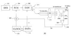
- FIG. 1depicts a typical transmitter 100 for ON-OFF-keying, Return-to-Zero (RZ) transmission and consists of a semiconductor distributed-feedback (DFB) laser 102 followed by a pulse carver modulator (PCM) 104 and an electroabsorption data modulator (EAM) 106 .
- the order of the EAM and PCMis reversible.
- the PCMis driven by an electronic clock 108 running at the line rate of the system (10 GHz, for example) and produces a train of RZ pulses from the DFB laser output to act as a carrier for data.
- a phase shifter 112is also typically placed between the clock 108 and the PCM 104 to initialize transmitter timing.
- An electronic data pulse stream to be transmitted(consisting of, for example, a series of square electric pulses representing 1's and 0's of binary data D from data module 110 ) modulates the optical transmission of the EAM, and the data is encoded into an optical pulse train. The final output of the two modulators is an optically modulated data pulse train.
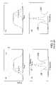
- FIG. 2Adepicts a case in which the optical pulse from the PCM enters the EAM too early and leads the data pulse.
- a positive chirpis introduced into the data (a change in frequency ⁇ and as seen by the dotted line above the data and timing curves in FIG. 2A ).
- the spectral analysis of the timing conditions of FIG. 2Ais shown in FIG. 2B wherein a center frequency (CF) is flanked by asymmetrical lower sideband (LSB) and upper sideband (USB).
- the reverse conditionswherein the optical pulse lags behind the data pulse is seen in FIG. 2C .
- spectral analysis(as shown in FIG. 2D ) reveals that the asymmetry of the upper and lower sidebands still exists, but is reversed from the previous condition.
- the data pulse and the pulsed optical output of the PCMshare a common center point with respect to time (denoted by (x) in FIGS. 2A and C).
- chirpis minimized and the spectral analysis reveals symmetrical upper and lower sideband modulation levels.
- the timing drift in real devicestends to be random and thus the optical data will suffer from random chirping without an active management of the timing between the PCM and EAM.
- an apparatus for LH and ULH DWDM transmissionthat is capable of synchronizing the pulse carver modulator and electroabsorption data modulator and a concomitant method for establishing such operational conditions.
- the present inventionprovides an apparatus for the synchronization of a pulse carver modulator and electroabsorption data modulator used in an optical transmitter for optical telecommunication. It includes a first, pulse carver modulator to generate a RZ optical pulse train, a second, electroabsorption modulator to encode the data onto the optical pulse train, an optical filter to resolve upper and lower modulation sidebands of the RZ optical data, and an analyzer to measure the relative optical power of the two modulation side bands and convert the received optical power of the sidebands into a control signal for synchronizing the two modulators.
- the present inventionalso includes a voltage-controlled phase shifter to control the relative timing between the pulse carver modulator and electroabsorption modulator via the control signal and optical power splitters to tap a portion of the optical data into at least two portions.
- a semiconductor DFB laseris used and a Lithium Niobate amplitude modulator is used for pulse carving.
- a wedged etalonis used as a filter element to select the USB and LSB from the spectrum of the optical data.
- the filteris slightly wedged such that the thickness varies linearly along its cross-section and the transmission frequency changes accordingly.
- the analyzercontains two substantially identical photo-detectors to measure the optical power of the filtered USB and LSB.
- An electronic differential amplifiertakes the signal from the two photo-detectors and produces a control signal proportional to the difference of the powers of USB and LSB.
- the phase shifterin response to said control signal, adapts the temporal delay of the electronic drive of the pulse carver modulator in a manner that reduces differences between the relative power levels of said upper and lower sidebands.
- the inventionalso includes a method for synchronizing pulses from an optical carver and a data modulator that has steps of providing a data bearing optical signal in response to a sequence of optical signal carrier pulses and data pulses, determining at least a relative signal strength of upper and lower modulation sidebands associated with the data bearing optical signal and in response to the determined relative signal strength, adapting the sequence of optical signal carrier pulses in a manner tending to reduce differences between the signal strength of the upper and lower modulation sidebands.
- the determining stepincludes splitting the data bearing optical signal into a plurality of optical signal portions, passing at least two of the optical signal portions through a filter element to produce filtered optical signal portions having respective center frequencies offset from an initial center frequency of a predetermined amount and detecting a power level of each of the at least two filtered optical signal portions.
- the adapting stepincludes applying a control signal to a shifting device for adjusting an optical signal carrier pulse rate, the control signal being indicative of the differences in signal strength between the lower and upper modulation sidebands.
- FIG. 1depicts a prior art optical transmitter for optical communication
- FIG. 2depicts instances of temporal misalignment between the pulse carver and data modulation in FIG. 1 and the spectral consequences of such misalignments;
- FIG. 3depicts an optical transmitter in accordance with the subject invention
- FIG. 4depicts a graph of timing misalignment vs. power differences of the USB and LSB
- FIG. 5is a detailed view of a filter element of the system of the subject invention.
- FIG. 6depicts a series of method steps in accordance with a method of the subject invention for fabricating the filter element
- FIG. 7depicts a series of method steps in accordance with the subject invention for synchronization of a pulse carver and a data modulator
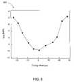
- FIG. 8depicts a graph of timing offset versus bit error rate, which plots specific results of an experiment conducted with the system of the subject invention.
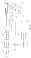
- FIG. 3depicts a system 300 for ultralong-haul dense wavelength division multiplexing (DWDM) transmission of data in an optical environment.
- the system 300contains a semiconductor distributed feedback laser (DFB) 302 and a pulse carver modulator (PCM) 304 .
- the PCM 304is a Lithium-Niobate PCM.
- the optical carrier frequency of the DFB laseris typically a multiple of 50 GHz as set by the industry standard.
- the PCM 304is driven by an electronic clock 312 running at the line rate of the communication network and produces a train of Return-to-Zero (RZ) optical carrier pulses from the DFB laser output.
- RZReturn-to-Zero
- An electronic data pulse stream to be transmitted(consisting of, for example, a series of square electric pulses representing 1's and 0's of binary data D from data module 310 ) modulates optical transmissions from an electroabsorption modulator (EAM) 306 , and results in the data being encoded into an optical pulse train (TX).
- the data module 310 and electronic clock 312are connected such that the data rate (10 Gbits/s, for example ) is identical to the repetition rate (10 GHz, for example) of the optical pulse train produced by the PCM 304 .
- a phase shifter 326temporally shifts the clock signal to the PCM 304 and hence controls the timing between the pulse carving in the PCM 304 and data modulation in the EAM 306 .
- data module 310communicates with the electronic clock 312 via control signals C.
- the electronic clock 312can send control signals to the data module 310 , thereby allowing for additional communication.
- modificationsare, but not limited to, replacement of the semiconductor DFB laser by a semiconductor tunable laser, the Lithium-Niobate PCM by a low-chirp EAM pulse carver, or the combination of the DFB laser and the Lithium-Niobate PCM by any low-chirp pulsed laser source, such as a mode-locked fiber laser.
- the order of the PCM 304 and EAM 306is interchangeable.
- the EAM's 306 primary taskis for data modulation and its operational characteristics are its polarization insensitivity and low drive voltage requirement. Examples of suitable components are JDS Uniphase QF935/208 for the DFB, Lucent X2623C for the PCM and Oki OM5642W-30B for the EAM.
- the inset in FIG. 4depicts the optical spectra (shifted by the optical carrier frequency) of the output TX of the transmitter 300 in FIG. 3 in the case when the pulse carver leads (solid curve) or lags (dashed curve) the EAM 306 by 20 ps.
- the measurement of the relative powers in the upper and lower sidebandsrequires a filter element 316 with a spectral resolution better than roughly a third of the modulation bandwitdth.
- the spectral measurement of the modulation sidebandsis most easily implemented using a wedged etalon as depicted in FIG. 3 . It has no moving parts unlike other filter elements, such as a scanning etalon.
- a small fraction ( ⁇ 10%) of the output signal (data-encoded optical pulse train) TXis connected to an optical splitter 314 to create a plurality of transmitted signals TX (e.g., three split signals TX).
- the split output signals TXare then passed through a wedged etalon filter 316 .
- the filter element 316is a fused silica substrate block 500 .
- the blockconsists of two planes, a first plane 502 and a second plane 504 .
- the second plane 504is angled with respect to first plane 502 .
- the angle of the second plane 504 with respect to the first plane 502is approximately 10 arcsec. The angle is calculated such that the first order modulation sideband frequencies on either side of the center frequency can be viewed over a desired linear spacing shift along the direction of the first plane 502 .
- the angle of the etalonis produced in such a manner so as to produce a 10 GHz transmission peak shift over approximately a 2 mm linear direction along first plane 502 .
- the filter thicknessvaries linearly along its cross-section.
- the wedge angle of 10 arcsecproduces a 10 GHz shift of the filter transmission peak for every 2 mm linear displacement of the light input position.
- the linear spacing between each of the three samples of the data-encoded optical pulse train TXis 2 mm.
- the wedged etalon filter 316can also function as a wavelength locker. More specifically, since the etalon 316 was specifically fabricated for filtering frequencies on the ITU grid, the output intensity from the second plane 504 at the center frequency point can be monitored so as to confirm that the DFB output wavelength is that which is expected for the system.
- the modulation sidebandsare analyzed (i.e., amount of power in each sideband is examined) by a spectral analyzer 318 to determine the extent of misalignment and generate correction signals accordingly.
- the spectral analyzer 318contains, among other components, a first detector 322 1 and a second detector 322 2 .
- the first detector 322 1analyzes the strength of the lower sideband and the second detector 322 2 analyzes the strength of the upper sideband of the output data-encoded optical pulse train TX.
- the first and second detectors 322 1 and 322 2are P-I-N diodes that are used to detect the intensity of the lower and upper sidebands, respectively.
- the diodesconvert the optical intensity into a lower sideband voltage signal (LSBV) and an upper sideband voltage signal (USBV).
- the LSBV and USBVare provided as inputs into a differential amplifier 324 to produce a differential control signal (DS).
- the differential control signal DSis a value that is indicative of the difference of the lower sideband and upper sideband modulation intensities. Accordingly, the greater the intensity difference between the lower and upper sidebands, the greater the relative shifting of the PCM optical pulse train from the center of the electrical data pulses in the EAM 306 ; hence, the larger the differential control signal DS.
- the differential control signal DSis provided as input to a phase shifter 326 .
- the phase shifter 326also receives as input, output signals from the electronic clock 312 .
- the phase shifter 326can adjust the temporal phase of the incoming clock signal information based upon the differential control signal DS thereby providing a temporal delay to the drive signal of PCM 304 .
- the optical carrier pulse train from PCM 304is shifted in time relative to the data modulation pulses applied to the EAM. For example, in a situation such as that shown in FIG.
- the differential control signal DSwill be such that the resultant timing control signals outputted from the phase shifter 326 brings the optical pulse closer to the center of the data pulses (“x” in FIG. 2A ).
- the differential control signal DSwill be such that the resultant timing control signals from the phase shifter 326 centers the optical pulses with respect to the data pulses.
- a method for producing the wedged etalon filter 316is shown as a series of method steps 600 of FIG. 6 .
- the method 600starts at step 602 and proceeds to step 604 where a fused silica substrate block is provided for further processing.
- the initial substrateis slightly thicker than the target thickness to account for the material loss owing to the etching process to be detailed. Other materials, including silicon, can also be used.
- the substrateis dipped into an etching solution in a time-controlled manner so as to reduce the thickness of the substrate in a graduated, linear manner.
- the substrateis silica and is dipped in an HF buffer solution of approximate concentration of 7% at an immersion rate of approximately 3 mm/min.
- the block substrateis altered so that two previously parallel planes (e.g., first plane 502 and pre-second plane 504 a ) are now at an angle of 10 arcsec with respect to each other.
- a reflective coatingis applied to first plane 502 and second plane 504 .
- the reflective coatingis approximately 80% and the resultant spectral resolution of the filter is 2 GHz, suitable for separating the modulation side bands at ⁇ 10 GHz.
- the methodends at step 610 with the completed etalon filter 316 .
- One skilled in the artwill realize that different angles and thicknesses of a given dispersion element can be formed depending upon system requirements and index of refraction of the initial substrate.
- a method for synchronizing the PCM 304 and the EAM 306is also disclosed in the subject invention and is specifically shown by the series of method steps 700 of FIG. 7 .
- the methodstarts at step 702 and proceeds to step 704 wherein samples of the data bearing optical pulse train are provided for further inspection and analysis.
- samples of the data bearing optical pulse trainare provided for further inspection and analysis.
- three samples of the optical dataare provided.
- the output spectral characteristics of the optical data pulsesare obtained.
- the output spectrum of the optical datais obtained by, for example, a specially designed etalon, which is capable of filtering the operating frequency of the optical element (laser) and also separating the first order upper and lower sidebands.
- the relative strength of the upper and lower sidebands of the output spectrumare determined. In one example, the relative strength of the upper and lower sidebands is determined by converting the output intensity of these frequencies into electrical signals.
- a correction signalis generated based upon the sideband information obtained from the determining step 708 .
- the electrical signals obtained by converting the intensity of the upper and lower sidebandsare used as inputs to a differential amplifier to generate an output amplifier signal.
- the correction signalis provided to a timing device. In one example of the invention, the output signal generated by the operational amplifier is provided to a RF phase shifter in the system.
- the phase shifter devicealters the timing of the generation of the optical pulse train in the PCM with respect to data pulses so as to center the optical pulses with respect to the data pulses. Successful centering the optical pulses with respect to the data pulses is observed by subsequent monitoring of the upper and lower sidebands of subsequent output data spectrums and observing smaller and smaller correction signals (eventually resulted in a zero value correction signal). The method ends at step 714 .
Landscapes
- Physics & Mathematics (AREA)
- Engineering & Computer Science (AREA)
- Computer Networks & Wireless Communication (AREA)
- Signal Processing (AREA)
- Optics & Photonics (AREA)
- Electromagnetism (AREA)
- Optical Communication System (AREA)
- Optical Modulation, Optical Deflection, Nonlinear Optics, Optical Demodulation, Optical Logic Elements (AREA)
Abstract
Description
Claims (29)
Priority Applications (1)
| Application Number | Priority Date | Filing Date | Title |
|---|---|---|---|
| US10/354,718US7209669B2 (en) | 2002-02-01 | 2003-01-30 | Method and apparatus for synchronizing a pulse carver and a data modulator for optical telecommunication |
Applications Claiming Priority (2)
| Application Number | Priority Date | Filing Date | Title |
|---|---|---|---|
| US35362802P | 2002-02-01 | 2002-02-01 | |
| US10/354,718US7209669B2 (en) | 2002-02-01 | 2003-01-30 | Method and apparatus for synchronizing a pulse carver and a data modulator for optical telecommunication |
Publications (2)
| Publication Number | Publication Date |
|---|---|
| US20030147114A1 US20030147114A1 (en) | 2003-08-07 |
| US7209669B2true US7209669B2 (en) | 2007-04-24 |
Family
ID=27669115
Family Applications (1)
| Application Number | Title | Priority Date | Filing Date |
|---|---|---|---|
| US10/354,718Expired - LifetimeUS7209669B2 (en) | 2002-02-01 | 2003-01-30 | Method and apparatus for synchronizing a pulse carver and a data modulator for optical telecommunication |
Country Status (1)
| Country | Link |
|---|---|
| US (1) | US7209669B2 (en) |
Cited By (5)
| Publication number | Priority date | Publication date | Assignee | Title |
|---|---|---|---|---|
| US20050041984A1 (en)* | 2003-08-12 | 2005-02-24 | Agilent Technologies Inc. | Electro-absorption modulation of optical signals |
| US20050226638A1 (en)* | 2001-10-09 | 2005-10-13 | Derek Nesset | Optical signal transmission |
| US20060171719A1 (en)* | 2005-02-03 | 2006-08-03 | Schmidt Theodore J | Optical transmission system having optimized filter wavelength offsets |
| US20100128356A1 (en)* | 2006-12-19 | 2010-05-27 | Dmitri Feklistov | Beam Blocking and Combining Optic |
| US10256934B2 (en)* | 2016-10-11 | 2019-04-09 | Zte Corporation | Chirp managed laser generation for next generation passive optical networks |
Families Citing this family (42)
| Publication number | Priority date | Publication date | Assignee | Title |
|---|---|---|---|---|
| US7330666B1 (en)* | 2003-01-31 | 2008-02-12 | Ciena Corporation | Method and apparatus for controlling modulator phase alignment in a transmitter of an optical communications system |
| US6963685B2 (en)* | 2002-07-09 | 2005-11-08 | Daniel Mahgerefteh | Power source for a dispersion compensation fiber optic system |
| US7263291B2 (en)* | 2002-07-09 | 2007-08-28 | Azna Llc | Wavelength division multiplexing source using multifunctional filters |
| US7663762B2 (en)* | 2002-07-09 | 2010-02-16 | Finisar Corporation | High-speed transmission system comprising a coupled multi-cavity optical discriminator |
| US7054538B2 (en)* | 2002-10-04 | 2006-05-30 | Azna Llc | Flat dispersion frequency discriminator (FDFD) |
| US7742542B2 (en)* | 2002-11-06 | 2010-06-22 | Finisar Corporation | Phase correlated quadrature amplitude modulation |
| US7280721B2 (en) | 2002-11-06 | 2007-10-09 | Azna Llc | Multi-ring resonator implementation of optical spectrum reshaper for chirp managed laser technology |
| US7558488B2 (en)* | 2002-11-06 | 2009-07-07 | Finisar Corporation | Reach extension by using external Bragg grating for spectral filtering |
| US7505694B2 (en)* | 2002-11-06 | 2009-03-17 | Finisar Corporation | Thermal chirp compensation systems for a chirp managed directly modulated laser (CML™) data link |
| US7536113B2 (en)* | 2002-11-06 | 2009-05-19 | Finisar Corporation | Chirp managed directly modulated laser with bandwidth limiting optical spectrum reshaper |
| US7564889B2 (en)* | 2002-11-06 | 2009-07-21 | Finisar Corporation | Adiabatically frequency modulated source |
| US7907648B2 (en)* | 2002-12-03 | 2011-03-15 | Finisar Corporation | Optical FM source based on intra-cavity phase and amplitude modulation in lasers |
| US7809280B2 (en)* | 2002-12-03 | 2010-10-05 | Finisar Corporation | Chirp-managed, electroabsorption-modulated laser |
| US7609977B2 (en)* | 2002-12-03 | 2009-10-27 | Finisar Corporation | Optical transmission using semiconductor optical amplifier (SOA) |
| US7813648B2 (en)* | 2002-12-03 | 2010-10-12 | Finisar Corporation | Method and apparatus for compensating for fiber nonlinearity in a transmission system |
| US7480464B2 (en)* | 2002-12-03 | 2009-01-20 | Finisar Corporation | Widely tunable, dispersion tolerant transmitter |
| US7474859B2 (en)* | 2002-12-03 | 2009-01-06 | Finisar Corporation | Versatile compact transmitter for generation of advanced modulation formats |
| US7542683B2 (en) | 2002-12-03 | 2009-06-02 | Finisar Corporation | Chirp Managed Laser (CML) transmitter |
| US7925172B2 (en)* | 2002-12-03 | 2011-04-12 | Finisar Corporation | High power, low distortion directly modulated laser transmitter |
| US7860404B2 (en)* | 2002-12-03 | 2010-12-28 | Finisar Corporation | Optical FM source based on intra-cavity phase and amplitude modulation in lasers |
| US7613401B2 (en)* | 2002-12-03 | 2009-11-03 | Finisar Corporation | Optical FM source based on intra-cavity phase and amplitude modulation in lasers |
| US7630425B2 (en)* | 2003-02-25 | 2009-12-08 | Finisar Corporation | Optical beam steering for tunable laser applications |
| US8792531B2 (en) | 2003-02-25 | 2014-07-29 | Finisar Corporation | Optical beam steering for tunable laser applications |
| US7639955B2 (en)* | 2004-09-02 | 2009-12-29 | Finisar Corporation | Method and apparatus for transmitting a signal using a chirp managed laser (CML) and an optical spectrum reshaper (OSR) before an optical receiver |
| US20070012860A1 (en)* | 2005-05-05 | 2007-01-18 | Daniel Mahgerefteh | Optical source with ultra-low relative intensity noise (RIN) |
| US7697186B2 (en)* | 2006-10-24 | 2010-04-13 | Finisar Corporation | Spectral response modification via spatial filtering with optical fiber |
| US7962045B2 (en) | 2006-12-22 | 2011-06-14 | Finisar Corporation | Optical transmitter having a widely tunable directly modulated laser and periodic optical spectrum reshaping element |
| US7941057B2 (en) | 2006-12-28 | 2011-05-10 | Finisar Corporation | Integral phase rule for reducing dispersion errors in an adiabatically chirped amplitude modulated signal |
| US8131157B2 (en)* | 2007-01-22 | 2012-03-06 | Finisar Corporation | Method and apparatus for generating signals with increased dispersion tolerance using a directly modulated laser transmitter |
| EP2111678B1 (en) | 2007-02-02 | 2015-04-08 | Finisar Corporation | Temperature stabilizing packaging for optoelectronic components in a transmitter module |
| US8027593B2 (en) | 2007-02-08 | 2011-09-27 | Finisar Corporation | Slow chirp compensation for enhanced signal bandwidth and transmission performances in directly modulated lasers |
| US7991291B2 (en) | 2007-02-08 | 2011-08-02 | Finisar Corporation | WDM PON based on DML |
| US7697847B2 (en)* | 2007-04-02 | 2010-04-13 | Finisar Corporation | Dispersion compensator for frequency reshaped optical signals |
| US8204386B2 (en)* | 2007-04-06 | 2012-06-19 | Finisar Corporation | Chirped laser with passive filter element for differential phase shift keying generation |
| US7991297B2 (en) | 2007-04-06 | 2011-08-02 | Finisar Corporation | Chirped laser with passive filter element for differential phase shift keying generation |
| US7760777B2 (en)* | 2007-04-13 | 2010-07-20 | Finisar Corporation | DBR laser with improved thermal tuning efficiency |
| US7778295B2 (en)* | 2007-05-14 | 2010-08-17 | Finisar Corporation | DBR laser with improved thermal tuning efficiency |
| US8160455B2 (en)* | 2008-01-22 | 2012-04-17 | Finisar Corporation | Method and apparatus for generating signals with increased dispersion tolerance using a directly modulated laser transmitter |
| WO2009114738A2 (en) | 2008-03-12 | 2009-09-17 | Hypres, Inc. | Digital radio-frequency tranceiver system and method |
| US7869473B2 (en)* | 2008-03-21 | 2011-01-11 | Finisar Corporation | Directly modulated laser with isolated modulated gain electrode for improved frequency modulation |
| US8260150B2 (en)* | 2008-04-25 | 2012-09-04 | Finisar Corporation | Passive wave division multiplexed transmitter having a directly modulated laser array |
| US8199785B2 (en) | 2009-06-30 | 2012-06-12 | Finisar Corporation | Thermal chirp compensation in a chirp managed laser |
Citations (11)
| Publication number | Priority date | Publication date | Assignee | Title |
|---|---|---|---|---|
| US5068864A (en)* | 1990-05-04 | 1991-11-26 | Laser Science, Inc. | Laser frequency stabilization |
| US5274659A (en)* | 1992-02-18 | 1993-12-28 | At&T Bell Laboratories | Harmonically mode-locked laser |
| US5524076A (en)* | 1994-01-28 | 1996-06-04 | Northern Telecom Limited | Chirp control of a Mach-Zehnder optical modulator using non-equal power splitting |
| US20020001115A1 (en)* | 2000-06-30 | 2002-01-03 | Kazuyuki Ishida | Optical transmission apparatus, and output stabilization control method for an optical modulator used in the optical transmission apparatus |
| US20020044322A1 (en)* | 2000-09-08 | 2002-04-18 | The Regents Of The University Of California | Methods for monitoring performance in optical networks |
| US20020071184A1 (en)* | 2000-02-10 | 2002-06-13 | Yasuhiro Nishi | Etalon filter |
| US6671079B2 (en)* | 2001-12-14 | 2003-12-30 | Lucent Technologies Inc. | Method and apparatus for transmitting a modulated optical signal |
| US6766116B2 (en)* | 2000-01-12 | 2004-07-20 | Alcatel | Optical transmission system |
| US20050135439A1 (en)* | 2001-07-06 | 2005-06-23 | Chapman William B. | External cavity laser method and apparatus with orthogonal tuning of laser wavelength and cavity optical path length |
| US20050271393A1 (en)* | 2000-11-28 | 2005-12-08 | Gnauck Alan H | System for mitigating the effects of fiber dispersion by separate detection of two transmitted sidbands |
| US7079772B2 (en)* | 2001-06-01 | 2006-07-18 | Nortel Networks Limited | Optical signal generator with stabilized carrier frequency output |
- 2003
- 2003-01-30USUS10/354,718patent/US7209669B2/ennot_activeExpired - Lifetime
Patent Citations (11)
| Publication number | Priority date | Publication date | Assignee | Title |
|---|---|---|---|---|
| US5068864A (en)* | 1990-05-04 | 1991-11-26 | Laser Science, Inc. | Laser frequency stabilization |
| US5274659A (en)* | 1992-02-18 | 1993-12-28 | At&T Bell Laboratories | Harmonically mode-locked laser |
| US5524076A (en)* | 1994-01-28 | 1996-06-04 | Northern Telecom Limited | Chirp control of a Mach-Zehnder optical modulator using non-equal power splitting |
| US6766116B2 (en)* | 2000-01-12 | 2004-07-20 | Alcatel | Optical transmission system |
| US20020071184A1 (en)* | 2000-02-10 | 2002-06-13 | Yasuhiro Nishi | Etalon filter |
| US20020001115A1 (en)* | 2000-06-30 | 2002-01-03 | Kazuyuki Ishida | Optical transmission apparatus, and output stabilization control method for an optical modulator used in the optical transmission apparatus |
| US20020044322A1 (en)* | 2000-09-08 | 2002-04-18 | The Regents Of The University Of California | Methods for monitoring performance in optical networks |
| US20050271393A1 (en)* | 2000-11-28 | 2005-12-08 | Gnauck Alan H | System for mitigating the effects of fiber dispersion by separate detection of two transmitted sidbands |
| US7079772B2 (en)* | 2001-06-01 | 2006-07-18 | Nortel Networks Limited | Optical signal generator with stabilized carrier frequency output |
| US20050135439A1 (en)* | 2001-07-06 | 2005-06-23 | Chapman William B. | External cavity laser method and apparatus with orthogonal tuning of laser wavelength and cavity optical path length |
| US6671079B2 (en)* | 2001-12-14 | 2003-12-30 | Lucent Technologies Inc. | Method and apparatus for transmitting a modulated optical signal |
Cited By (9)
| Publication number | Priority date | Publication date | Assignee | Title |
|---|---|---|---|---|
| US20050226638A1 (en)* | 2001-10-09 | 2005-10-13 | Derek Nesset | Optical signal transmission |
| US7336906B2 (en)* | 2001-10-09 | 2008-02-26 | Ericsson Ab | Optical signal transmission |
| US20050041984A1 (en)* | 2003-08-12 | 2005-02-24 | Agilent Technologies Inc. | Electro-absorption modulation of optical signals |
| US7466927B2 (en)* | 2003-08-12 | 2008-12-16 | Avago Technologies Fiber Ip (Singapore) Pte. Ltd. | Electro-absorption modulation of optical signals |
| US20060171719A1 (en)* | 2005-02-03 | 2006-08-03 | Schmidt Theodore J | Optical transmission system having optimized filter wavelength offsets |
| US7437080B2 (en)* | 2005-02-03 | 2008-10-14 | Stratalight Communications, Inc. | Optical transmission system having optimized filter wavelength offsets |
| US20100128356A1 (en)* | 2006-12-19 | 2010-05-27 | Dmitri Feklistov | Beam Blocking and Combining Optic |
| US7986463B2 (en)* | 2006-12-19 | 2011-07-26 | Ellex Medical Pty Ltd | Beam blocking and combining optic |
| US10256934B2 (en)* | 2016-10-11 | 2019-04-09 | Zte Corporation | Chirp managed laser generation for next generation passive optical networks |
Also Published As
| Publication number | Publication date |
|---|---|
| US20030147114A1 (en) | 2003-08-07 |
Similar Documents
| Publication | Publication Date | Title |
|---|---|---|
| US7209669B2 (en) | Method and apparatus for synchronizing a pulse carver and a data modulator for optical telecommunication | |
| CN1270452C (en) | Wavelength control using dither modulation and feedback | |
| US7512338B2 (en) | Method and apparatus for pulse generation and adaptive pulse generation for optical communications | |
| EP1703651B1 (en) | Method and system for automatic feedback control for fine tuning a delay interferometer | |
| US7536108B2 (en) | High precision chromatic dispersion measuring method and automatic dispersion compensating optical link system that uses this method | |
| US7333736B2 (en) | Method and apparatus for controlling modulator phase alignment in a transmitter of an optical communications system | |
| US7398023B2 (en) | Method and apparatus for bias and alignment control in an optical signal transmitter | |
| US20020063935A1 (en) | Optical transmission systems including upconverter apparatuses and methods | |
| US20020076132A1 (en) | Optical filter for simultaneous single sideband modulation and wavelength stabilization | |
| US6891995B2 (en) | Wavelength division multiplex transmission system | |
| US6674936B2 (en) | Polarization mode dispersion compensation using a wavelength locked loop | |
| US7062166B2 (en) | First and second derivative processing of wavelength multiplexed optical signals | |
| US7330666B1 (en) | Method and apparatus for controlling modulator phase alignment in a transmitter of an optical communications system | |
| EP1617576A1 (en) | Bandwidth limited frequency shift keying modulation format | |
| US20060088321A1 (en) | Closed loop RZ-DPSK alignment for optical communications | |
| US7068944B2 (en) | Multi-function optical performance monitor | |
| US6654152B2 (en) | Frequency guiding filter for dispersion managed soliton transmission | |
| US6597840B2 (en) | Tunable fiber Bragg gratings and wavelength-locked loops for dispersion compensation | |
| US20040067067A1 (en) | Optical frequency controlling device for ultra-dense wavelength-division-multiplexed optical channels | |
| US7444079B2 (en) | Optical power control monitor for multiple wavelength fiber-optic networks | |
| Kang et al. | A novel method for synchronizing the pulse carver and electroabsorption data modulator for ultralong-haul DWDM transmission | |
| JP2009081484A (en) | Fm modulation measurement method |
Legal Events
| Date | Code | Title | Description |
|---|---|---|---|
| AS | Assignment | Owner name:LUCENT TECHNOLOGIES INC., NEW JERSEY Free format text:ASSIGNMENT OF ASSIGNORS INTEREST;ASSIGNORS:KANG, INUK;MOLLENAUER, LINN FREDERICK;REEL/FRAME:013723/0286 Effective date:20030129 | |
| STCF | Information on status: patent grant | Free format text:PATENTED CASE | |
| FPAY | Fee payment | Year of fee payment:4 | |
| FPAY | Fee payment | Year of fee payment:8 | |
| AS | Assignment | Owner name:PROVENANCE ASSET GROUP LLC, CONNECTICUT Free format text:ASSIGNMENT OF ASSIGNORS INTEREST;ASSIGNORS:NOKIA TECHNOLOGIES OY;NOKIA SOLUTIONS AND NETWORKS BV;ALCATEL LUCENT SAS;REEL/FRAME:043877/0001 Effective date:20170912 Owner name:NOKIA USA INC., CALIFORNIA Free format text:SECURITY INTEREST;ASSIGNORS:PROVENANCE ASSET GROUP HOLDINGS, LLC;PROVENANCE ASSET GROUP LLC;REEL/FRAME:043879/0001 Effective date:20170913 Owner name:CORTLAND CAPITAL MARKET SERVICES, LLC, ILLINOIS Free format text:SECURITY INTEREST;ASSIGNORS:PROVENANCE ASSET GROUP HOLDINGS, LLC;PROVENANCE ASSET GROUP, LLC;REEL/FRAME:043967/0001 Effective date:20170913 | |
| FEPP | Fee payment procedure | Free format text:MAINTENANCE FEE REMINDER MAILED (ORIGINAL EVENT CODE: REM.); ENTITY STATUS OF PATENT OWNER: LARGE ENTITY | |
| AS | Assignment | Owner name:ALCATEL-LUCENT USA INC., NEW JERSEY Free format text:CHANGE OF NAME;ASSIGNOR:LUCENT TECHNOLOGIES INC.;REEL/FRAME:049887/0613 Effective date:20081101 | |
| AS | Assignment | Owner name:NOKIA US HOLDINGS INC., NEW JERSEY Free format text:ASSIGNMENT AND ASSUMPTION AGREEMENT;ASSIGNOR:NOKIA USA INC.;REEL/FRAME:048370/0682 Effective date:20181220 | |
| FEPP | Fee payment procedure | Free format text:11.5 YR SURCHARGE- LATE PMT W/IN 6 MO, LARGE ENTITY (ORIGINAL EVENT CODE: M1556); ENTITY STATUS OF PATENT OWNER: LARGE ENTITY | |
| MAFP | Maintenance fee payment | Free format text:PAYMENT OF MAINTENANCE FEE, 12TH YEAR, LARGE ENTITY (ORIGINAL EVENT CODE: M1553); ENTITY STATUS OF PATENT OWNER: LARGE ENTITY Year of fee payment:12 | |
| AS | Assignment | Owner name:PROVENANCE ASSET GROUP LLC, CONNECTICUT Free format text:RELEASE BY SECURED PARTY;ASSIGNOR:CORTLAND CAPITAL MARKETS SERVICES LLC;REEL/FRAME:058983/0104 Effective date:20211101 Owner name:PROVENANCE ASSET GROUP HOLDINGS LLC, CONNECTICUT Free format text:RELEASE BY SECURED PARTY;ASSIGNOR:CORTLAND CAPITAL MARKETS SERVICES LLC;REEL/FRAME:058983/0104 Effective date:20211101 Owner name:PROVENANCE ASSET GROUP LLC, CONNECTICUT Free format text:RELEASE BY SECURED PARTY;ASSIGNOR:NOKIA US HOLDINGS INC.;REEL/FRAME:058363/0723 Effective date:20211129 Owner name:PROVENANCE ASSET GROUP HOLDINGS LLC, CONNECTICUT Free format text:RELEASE BY SECURED PARTY;ASSIGNOR:NOKIA US HOLDINGS INC.;REEL/FRAME:058363/0723 Effective date:20211129 | |
| AS | Assignment | Owner name:RPX CORPORATION, CALIFORNIA Free format text:ASSIGNMENT OF ASSIGNORS INTEREST;ASSIGNOR:PROVENANCE ASSET GROUP LLC;REEL/FRAME:059352/0001 Effective date:20211129 | |
| AS | Assignment | Owner name:BARINGS FINANCE LLC, AS COLLATERAL AGENT, NORTH CAROLINA Free format text:PATENT SECURITY AGREEMENT;ASSIGNOR:RPX CORPORATION;REEL/FRAME:063429/0001 Effective date:20220107 | |
| AS | Assignment | Owner name:RPX CORPORATION, CALIFORNIA Free format text:RELEASE OF LIEN ON PATENTS;ASSIGNOR:BARINGS FINANCE LLC;REEL/FRAME:068328/0278 Effective date:20240802 | |
| AS | Assignment | Owner name:BARINGS FINANCE LLC, AS COLLATERAL AGENT, NORTH CAROLINA Free format text:PATENT SECURITY AGREEMENT;ASSIGNORS:RPX CORPORATION;RPX CLEARINGHOUSE LLC;REEL/FRAME:068328/0674 Effective date:20240802 |