US7209525B2 - Clock and data recovery with extended integration cycles - Google Patents
Clock and data recovery with extended integration cyclesDownload PDFInfo
- Publication number
- US7209525B2 US7209525B2US10/298,892US29889202AUS7209525B2US 7209525 B2US7209525 B2US 7209525B2US 29889202 AUS29889202 AUS 29889202AUS 7209525 B2US7209525 B2US 7209525B2
- Authority
- US
- United States
- Prior art keywords
- integrator
- integration
- input data
- data stream
- integrators
- Prior art date
- Legal status (The legal status is an assumption and is not a legal conclusion. Google has not performed a legal analysis and makes no representation as to the accuracy of the status listed.)
- Expired - Fee Related, expires
Links
- 230000010354integrationEffects0.000titleclaimsabstractdescription75
- 238000011084recoveryMethods0.000titleabstractdescription35
- 230000007704transitionEffects0.000claimsdescription29
- 238000005070samplingMethods0.000claimsdescription23
- 238000000034methodMethods0.000claimsdescription16
- 238000012545processingMethods0.000claimsdescription6
- 230000008569processEffects0.000claimsdescription5
- 230000035945sensitivityEffects0.000abstractdescription4
- 230000000630rising effectEffects0.000description15
- 238000010586diagramMethods0.000description11
- 101000767160Saccharomyces cerevisiae (strain ATCC 204508 / S288c) Intracellular protein transport protein USO1Proteins0.000description5
- 238000004891communicationMethods0.000description5
- 102100041002Forkhead box protein H1Human genes0.000description4
- 230000001360synchronised effectEffects0.000description4
- 101150053895Foxh1 geneProteins0.000description2
- 101000892840Homo sapiens Forkhead box protein H1Proteins0.000description2
- 101100348848Mus musculus Notch4 geneProteins0.000description2
- 230000005540biological transmissionEffects0.000description2
- 101100446506Mus musculus Fgf3 geneProteins0.000description1
- 101100317378Mus musculus Wnt3 geneProteins0.000description1
- 230000003247decreasing effectEffects0.000description1
- 230000007812deficiencyEffects0.000description1
- 238000013461designMethods0.000description1
- 230000009977dual effectEffects0.000description1
- 238000002372labellingMethods0.000description1
- 238000013507mappingMethods0.000description1
- 238000012986modificationMethods0.000description1
- 230000004048modificationEffects0.000description1
- 230000003287optical effectEffects0.000description1
- 230000001960triggered effectEffects0.000description1
Images


Classifications
- H—ELECTRICITY
- H04—ELECTRIC COMMUNICATION TECHNIQUE
- H04L—TRANSMISSION OF DIGITAL INFORMATION, e.g. TELEGRAPHIC COMMUNICATION
- H04L7/00—Arrangements for synchronising receiver with transmitter
- H04L7/02—Speed or phase control by the received code signals, the signals containing no special synchronisation information
- H04L7/033—Speed or phase control by the received code signals, the signals containing no special synchronisation information using the transitions of the received signal to control the phase of the synchronising-signal-generating means, e.g. using a phase-locked loop
- H04L7/0332—Speed or phase control by the received code signals, the signals containing no special synchronisation information using the transitions of the received signal to control the phase of the synchronising-signal-generating means, e.g. using a phase-locked loop with an integrator-detector
- H—ELECTRICITY
- H03—ELECTRONIC CIRCUITRY
- H03L—AUTOMATIC CONTROL, STARTING, SYNCHRONISATION OR STABILISATION OF GENERATORS OF ELECTRONIC OSCILLATIONS OR PULSES
- H03L7/00—Automatic control of frequency or phase; Synchronisation
- H03L7/06—Automatic control of frequency or phase; Synchronisation using a reference signal applied to a frequency- or phase-locked loop
- H03L7/08—Details of the phase-locked loop
- H03L7/081—Details of the phase-locked loop provided with an additional controlled phase shifter
- H03L7/0812—Details of the phase-locked loop provided with an additional controlled phase shifter and where no voltage or current controlled oscillator is used
- H—ELECTRICITY
- H04—ELECTRIC COMMUNICATION TECHNIQUE
- H04L—TRANSMISSION OF DIGITAL INFORMATION, e.g. TELEGRAPHIC COMMUNICATION
- H04L7/00—Arrangements for synchronising receiver with transmitter
- H04L7/02—Speed or phase control by the received code signals, the signals containing no special synchronisation information
- H04L7/033—Speed or phase control by the received code signals, the signals containing no special synchronisation information using the transitions of the received signal to control the phase of the synchronising-signal-generating means, e.g. using a phase-locked loop
- H—ELECTRICITY
- H03—ELECTRONIC CIRCUITRY
- H03L—AUTOMATIC CONTROL, STARTING, SYNCHRONISATION OR STABILISATION OF GENERATORS OF ELECTRONIC OSCILLATIONS OR PULSES
- H03L7/00—Automatic control of frequency or phase; Synchronisation
- H03L7/06—Automatic control of frequency or phase; Synchronisation using a reference signal applied to a frequency- or phase-locked loop
- H03L7/08—Details of the phase-locked loop
- H03L7/085—Details of the phase-locked loop concerning mainly the frequency- or phase-detection arrangement including the filtering or amplification of its output signal
- H03L7/089—Details of the phase-locked loop concerning mainly the frequency- or phase-detection arrangement including the filtering or amplification of its output signal the phase or frequency detector generating up-down pulses
- H03L7/0891—Details of the phase-locked loop concerning mainly the frequency- or phase-detection arrangement including the filtering or amplification of its output signal the phase or frequency detector generating up-down pulses the up-down pulses controlling source and sink current generators, e.g. a charge pump
- H03L7/0893—Details of the phase-locked loop concerning mainly the frequency- or phase-detection arrangement including the filtering or amplification of its output signal the phase or frequency detector generating up-down pulses the up-down pulses controlling source and sink current generators, e.g. a charge pump the up-down pulses controlling at least two source current generators or at least two sink current generators connected to different points in the loop
Definitions
- the present inventionrelates to clock and data recovery systems and, more specifically, to integrator-based front ends and bang-bang phase detectors for clock and data recovery.
- High-speed serial linksare commonly used for chip-to-chip interconnects in high-speed network systems.
- SONETsynchronous optical network
- OC-768 applicationsmay utilize 16 channels of 2.5 GB/s to support full duplex I/O of 40 GB/s.
- Many high-speed communications systemsuse asynchronous communication, where data is transmitted without a separate clock signal. Since a separate clock signal is not used, at a receiver side of a communications system, clock recovery circuitry is employed to extract intrinsic clock information from incoming data signals. Once extracted, the recovered clock is then used to re-time and regenerate the data originally transmitted.
- Such a clock and data recovery (CDR) circuittypically includes a voltage-controlled oscillator, a phase-locked loop (PLL), and/or a delay-locked loop (DLL) circuit as part of the clock recovery circuit, as well as deserialization logic as part of the data recovery circuit.
- PLLphase-locked loop
- DLLdelay-locked loop
- Various techniquesare used within CDR systems. Many of these are discussed in Sidiropoulos, S., and Horowitz, M., “A Semidigital Dual Delay-Locked Loop,” IEEE Journal of Solid-State Circuits, vol. 32, no. 11, November 1997, incorporated herein by reference.
- CDR systemssuffer from extreme sensitivity to clock skew between clock domains within the CDR circuit. This is because, in these systems, the goal is to generate recovered clock edges which are ideally located to allow registration of the incoming data at a point of maximum signal quality. Given the high-speed nature of these systems and the relatively low noise margin, even minor errors in the alignment of clock edges to data availability may result in erroneous data being captured. Managing this problem in the context of a typical GHz-rate deserializer requires extreme care to be used in matching of the clock paths and balancing of the clock distribution system. In a typical 10 GHz system, the allowable timing uncertainty when the system is set for maximum sensitivity can be as low as 5 ps. Alternatively, accepting a greater timing uncertainty reduces jitter tolerance due to degraded signal-to-noise ratio (SNR).
- SNRsignal-to-noise ratio
- clock and data recovery circuitryincludes a four-way interleaved sampler, where each integrator in the sampler integrates the input data for two unit intervals (UIs) and each integrator is sampled at or near the middle of its two-UI integration cycle.
- the reset cycle of each integratormay begin many tens of picoseconds after the data is sampled. Since the signal is sampled near the center of the integration cycle and is not highly proximate to the time of the integrator reset, the latch signal has a window of uncertainty extending into the length of a data bit cell with little possibility of latching erroneous data.
- the sensitivity of the clock recovery circuitrymay be optimized by centering the latch function over the time of highest signal level, thereby maximizing signal-to-noise ratio.
- the present inventionis a method for recovering data from an input data stream.
- the methodincludes integrating the input data stream using multiple independent integrators that are operating out-of-phase relative to one another, wherein at least one integrator has an integration period of more than one unit interval (UI) and processing the output of each integrator to recover the data from the input data stream.
- UIunit interval
- the present inventionis an apparatus for recovering data from an input data stream.
- the apparatusincludes multiple independent integrators configured to integrate the input data stream, wherein the integrators operate out-of-phase relative to one another, wherein at least one integrator has an integration period of more than one unit interval (UI). It also includes circuitry configured to process the output of each integrator to recover the data from the input data stream.
- UIunit interval
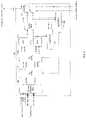
- FIG. 1is a block diagram illustrating an asynchronous serializer/deserializer (SerDes) communications system in accordance with one embodiment of the present invention.
- SerDesserializer/deserializer
- FIG. 2is a top-level block diagram illustrating receiver 114 of FIG. 1 .
- FIG. 3is a block diagram illustrating front-end 202 of FIG. 2 .
- FIG. 4is a timing diagram of the signals associated with front-end 202 of FIG. 2 .
- FIG. 5is a block diagram illustrating clock recovery circuit 206 of FIG. 2 .
- FIG. 6is a block diagram illustrating the logic of phase detector (PD) 502 of FIG. 5 .
- FIG. 7depicts TABLE 1 , which summarizes the logic of F/S logic gates 602 and 604 of FIG. 6 .
- a signal name with lowercase “p” or “n” appended to itis used to indicate the “positive” or “negative” element, respectively, of a differential pair.
- an uppercase “B” for “bar” appended to a signal nameis used to indicate the inverted copy of that signal.
- an uppercase “Q” appended to a signal nameindicates that it is the quadrature-phase (i.e., 90-degree) shifted version of that signal.
- CLK 2 Iis the collective name for the differential signal pair consisting of CLK 2 Ip and CLK 2 In
- CLK 2 IBis the inverted version of CLK 2 I
- CLK 2 QBis an inverted copy of the quadrature-phase shifted version of CLK 2 I.
- dotted linesare used to represent differential signal pairs.
- the dotted line labeled “Serial Data In” (SDIN) 112 in FIG. 1represents, collectively, SDINp and SDINn, the positive and negative elements, respectively, of the differential pair SDIN 112 .
- Thick linesare used to designate a bus, while thin lines are used to indicate a single signal.
- FIG. 1is a block diagram illustrating an asynchronous serializer/deserializer (SerDes) communications system in accordance with one embodiment of the present invention.
- SerDesserializer/deserializer
- FIG. 1parallel transmit (XMT) data vector 102 is fed to transmitter 104 .
- Transmitter 104receives the parallel data along with the differential transmission clock from transmitter-local voltage-controlled oscillator (VCO) and/or phase-locked loop (PLL) 106 .
- VCOvoltage-controlled oscillator
- PLLphase-locked loop
- the transmitterloads the parallel data into a shift register and uses the I and Q clocks to generate a transmit clock, which is used to serially “clock-out” the contents of the shift register.
- the resulting serial data out 108is output from transmitter 104 and transmitted across transmission medium 110 to receiver 114 .
- serial data in 112is received, sampled with a local clock that is a function of I and Q clocks from receiver-local VCO/PLL 116 , and deserialized into parallel receive (RCV) data vector 118 , which is output along with RCV clock (PRC) 120 .
- RCVparallel receive
- FIG. 2is a top-level block diagram illustrating the internals of receiver 114 of FIG. 1 .
- the receiverincludes four major circuits: (1) front-end 202 , (2) data recovery circuit 204 , (3) clock recovery circuit 206 , and (4) local clock generator 208 .
- the receiverperforms two major functions: (1) clock recovery and (2) data recovery.
- the clock recovery functionis divided between front-end 202 , clock recovery block 206 , and local clock generator 208 as well as data recovery circuit 204 .
- the data recovery functionis divided between front-end 202 and data recovery circuit 204 .
- the clock recovery functionserves to generate one or more local sampling clocks that are phase and frequency synchronized with the data transitions of the incoming data.
- Front-end 202serves, among other things, to sample the data transitions and integration results of the incoming data and provide this information to a phase detector within clock recovery circuit 206 .
- a delay-locked loop (DLL), also within clock recovery circuit 206uses the outputs of the phase detector to create an adjusted version, MIXO, of the local reference I and Q clocks.
- Local clock generator circuit 208(which is different from RCVR VCO/PLL 116 of FIG.
- front-end 202 and data recovery circuit 204use these local sampling clocks to sample, synchronize, and demultiplex (i.e., deserialize) the incoming serial data to achieve 16-bit parallel differential receive data vector (PRD) 118 clocked at one-sixteenth the incoming serial data rate.
- PRD 118may have a different number of bits per vector (e.g., 20 bits), and the output clock rate may be a different fraction of the incoming serial data rate (e.g., one-twentieth).
- the size and corresponding timing of the outputmay be configurable between two or more different sets of values (e.g., either 16-bit or 20-bit data).
- FIG. 3is a block diagram illustrating front-end 202 of FIG. 2 .
- front-end 202includes four integration circuits 302 , 304 , 306 , and 308 and two edge samplers 310 and 312 , each of which receives SDIN 112 and one of the four clock signals generated by local clock generator 208 of FIG. 2 .
- Each latch corresponding to an integratoroutputs a different bit of 4-bit output data vector OD
- each latch corresponding to an edge sampleroutputs a different bit of 2-bit output timing vector OT.
- each of integrators 302 , 304 , 306 , and 308integrates SDIN 112 corresponding to the period during which each integrator's corresponding integration clock is logic “1” and then holds its output in reset corresponding to the period during which each integrator's integration clock is logic “0.”
- the integration clocks for integrators 302 – 308are CLK 2 I, CLK 2 Q, CLK 2 IB, and CLK 2 QB, respectively.
- INT 1 302integrates SDIN 112 while the differential clock pair CLK 2 Ip and CLK 2 In (collectively represented by CLK 2 I) corresponds to logic “1.” This occurs when CLK 2 Ip is positive and CLK 2 In is negative. During this time, signal S 1 reflects the integration of the voltage corresponding to SDIN 112 . When CLK 2 I corresponds to logic “0,” the output of INT 1 302 is held in reset. During this time, both S 1 p and S 1 n are held at, or near, 0 volts differential.
- the integration clocks CLK 2 I, CLK 2 Q, CLK 2 IB, and CLK 2 IBare quarter-rate clocks
- the high (and low) period for each integration clockis approximately two unit intervals (UIs).
- the period of integration (and reset) for each integratoris also about two UIs.
- the integration clocks, by designare phase aligned to SDN 112 data transitions, the result is that each integrator performs the integration of two sequential bits of SDN 112 at a time.
- the integration periods for adjacent integratorsare overlapped by about one UI. Note that if the integration clocks were only high for only one UI, then no such overlap would occur.
- SDINpis illustrated as a series 402 of data values ⁇ b 1 , b 2 , b 3 , b 4 , b 5 , . . . ⁇ , where b 1 is both the first bit following the rising edge 404 of CLK 2 Ip as well as the first data bit into front-end 202 of FIG. 3 .
- b 1is both the first bit following the rising edge 404 of CLK 2 Ip as well as the first data bit into front-end 202 of FIG. 3 .
- INT 2 304 of FIG. 3integrates the values of b 2 and b 3 , resulting in the bell-shaped segment 416 of S 2 p , where S 2 p is seen to first fall to a maximum negative value corresponding to the integration of b 2 of value “0,” and then slope back up to “0” corresponding to the integration of b 3 of value “1” S 2 p is then held in reset when CLK 2 Qp is negative.
- INT 3 306 of FIG. 3integrates bits b 3 and b4 under control of CLK 2 IB
- INT 4 308 of FIG. 3integrates bits b 4 and b 5 under control of CLK 2 IB.
- Each latch utilized in this inventionoperates by sampling its input on the rising edge of its corresponding input clock, mapping that sample to a logic high or low state, and driving and holding the resulting “registered” state to the latch output until a subsequent rising edge of the input clock causes a transition in the output state.
- LATCH 1 314registers S 1 on the rising edge of CLK 2 Q
- LATCH 2 316registers S 2 on the rising edge of CLK 2 IB
- LATCH 3 320registers S 3 on the rising edge of CLK 2 QB
- LATCH 4 320registers S 4 on the rising edge of CLK 2 I.
- registration for each of latches 314 – 320occurs at or near the mid-point in the integration period of the corresponding integrator.
- registration for LATCH 1 314 of FIG. 3is triggered by the rising edge 422 of CLK 2 Qp, which occurs near the mid-point of segment 408 of the integration period for INT 1 302 of FIG. 3 .
- the systemis more tolerant to skew between the integrator reset control and the corresponding registration clock.
- the combination of the four integrators and their corresponding latchesfunctions as a 1:4 deserializer for SDIN 112 , from the serial format of SDIN 112 to a 4-bit “pseudo” parallel format, at one fourth the input data rate.
- OD 1 p , OD 2 p , OD 3 p , and OD 4 pare quarter-rate representations of the serial input data SDIN bits b 1 , b 2 , b 3 , and b 4 .
- OD 1 p , OD 2 p , OD 3 p , and OD 4 pare overlapped in time such that a single quarter-rate clock can be used to register them in parallel and drive them onto a quarter-rate bus.
- the term “quarter-rate”is with respect to the data rate of SDIN 112 .
- Edge samplers 310 and 312 of FIG. 3register the data stream at certain data transition edges of SDIN 112 .
- EDGE 1 310uses the rising edge of CLK 2 Qp to sample the data at the data transition point corresponding to the mid-point of integration for INT 1 302
- EDGE 2 312uses the rising edge of CLK 2 QBp to sample the data at the data transition point corresponding to the mid-point of integration for INT 3 306
- LATCH 6 322 and LATCH 7 324use the rising edges of CLK 2 IB and CLK 2 I, respectively, to register the respective outputs S 5 and S 6 of the edge samplers to synchronize them and stabilize them relative to the local clocking system.
- OT 1 pis in alignment with OD 2 p
- OT 2 pis in alignment with OD 4 p
- the edge sampler clocks CLK 2 Q and CLK 2 QBare early with respect to the data transition edges of SDIN 112 .
- the outputsthus reflect the value of data just prior to transition.
- OT 1is “1” ( 424 ), because b 1 is “1” ( 402 ) just prior to the rising edge of CLK 2 Qp.
- OT 2is “1” ( 426 ), because b 3 is “1” ( 428 ) just prior to the rising edge of CLK 2 QBp.
- front-end 202provides the four-bit parallel signal OD (i.e., bits OD 1 – 4 from latches 314 – 320 of FIG. 3 ) to data recovery circuit 204 , SYNC circuit 210 performs synchronization to the local sample clocks CLK 2 I, CLK 2 IB, CLK 2 Q, and CLK 2 QB producing a synchronized version SOC of the clock which will eventually be divided down to produce PRC 120 and a synchronized version SOD of data vector OD.
- ODfour-bit parallel signal OD
- DEMUX circuit 212is configurable to perform either a further 1:4 deserialization or a 1:5 deserialization, resulting in 16-bit or 20-bit, respectively, parallel RCV data vector (PRD) 118 clocked at one-sixteenth or one-twentieth, respectively, the data rate of SDIN 112 .
- PRDparallel RCV data vector
- front-end 202also performs edge sampling on SDIN 112 resulting in 2-bit output timing vector (OT).
- OToutput timing vector
- OD and OTboth feed clock recovery circuit 206 .
- OD and OTare used by control logic within clock recovery circuit 206 to adjust the phase and frequency of output MIXO relative to local differential reference I and Q clocks from the local receiver VCO/PLL.
- MIXOis adjusted so that the local sampling clocks CLK 2 I, CLK1B, CLK 2 Q, and CLK 2 QB, generated by divide-by-two, invert, and quadrature-phase shift circuitry of local clock generator 208 , are substantially aligned with the data transition edges of SDIN 112 at front-end 202 .
- Clock recovery circuit 206is based on a delay-locked loop (DLL) that performs continuous phase shifting of local differential reference I and Q clocks from the local receiver VCO/PLL, to create local sampling clocks whose phase is aligned with the transition edges of input data SDIN.
- DLLdelay-locked loop
- a voltage-controlled delay elementis employed in a DLL circuit to achieve the delay.
- One specific element used to realize this voltage-controlled delayis an analog quadrature mixer.
- the phase of output signal MIXOis thus directly controlled by the relative amplitudes of control signals VA and VB.
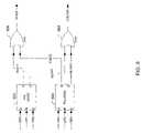
- FIG. 5shows a block diagram of clock recovery circuit 206 of FIG. 2 .
- circuit 206includes phase detector (PD) 502 , quadrant controller (Q-CTRL) 504 , amplitude controller (A-CTRL) 506 , charge pumps CPI 508 and CPQ 510 , mixer bias circuit 512 , amplitude detector (A-DETECT) 516 , quadrant detector (Q-DETECT) 518 , and mixer 514 .
- PDphase detector
- Q-CTRLquadrant controller
- A-CTRLamplitude controller
- charge pumps CPI 508 and CPQ 510charge pumps
- mixer bias circuit 512mixer bias circuit 512
- A-DETECTamplitude detector
- Q-DETECTquadrant detector
- PD 502uses the information in 4-bit data vector OD and 2-bit timing vector OT to decide (on a clock-by-clock basis) whether the locally generated differential clocks CLK 2 I, CLK 2 IB, CLK 2 Q and CLK 2 QB, which are functions of the output MIXO of mixer 514 , are running faster or slower than the intrinsic clock implicit in data stream SDIN 112 . If it determines that the local clocks are running fast, the PD 502 asserts a positive pulse on non-differential signal CFAST to quadrant controller (Q-CTRL) 504 . Otherwise, if it determines that the local clocks are running slow, then PD 502 asserts a positive pulse on non-differential signal CSLOW to Q-CTRL 504 .
- Q-CTRLquadrant controller
- FIG. 6illustrates the logic of CFAST and CSLOW generation performed by PD 502 of FIG. 5 .
- Each of fast/slow (F/S) logic circuits 602 and 604implements the logic of TABLE 1 of FIG. 7 , where F/S logic circuit 602 is fed by OD 1 , OT 1 , and OD 2 , while F/S logic circuit 604 is fed by OD 3 , OT 2 , and OD 4 .
- F/S logic circuits 602 and 604independently determine whether the clock is fast or slow according to the logic in TABLE 1 and output their conclusions to OR gates 606 and 608 .
- F/S logic circuit 602outputs (a) signal FAST 1 to FAST gate 606 and (b) signal SLOW 1 to SLOW gate 608 .
- F/S LOGIC circuit 604outputs (a) signal FAST 2 to FAST gate 606 and (b) signal SLOW 2 to SLOW gate 608 .
- the OR gates 606 and 608could each be replaced with a 2 to 1 multiplexor switched to allow the active signals to pass, or equivalently, each OR gate could be replaced with a “wired OR” arrangement.
- the column headingsindicate the input and output ports (and corresponding signals) for F/S logic circuits 602 and 604 of FIG. 6 .
- port Areceives OD 1
- port Breceives OT 1
- port Creceives OD 2
- port Dprovides FAST 1
- port Eprovides SLOW 1
- port Areceives OD 3
- port Breceives OT 2
- port Creceives OD 4
- port Dprovides FAST 2
- port Eprovides SLOW 2 .
- Rows 1 – 8 of TABLE 1correspond to the eight different possible combinations of input values to ports A, B, and C and the associated outputs provided at ports D and E.
- segments 434 and 436of the output signals OD 1 and OD 2 , respectively, convey (in a manner timed appropriately for F/S logic 602 ) the logic states of bits b 1 402 and b 2 430 , respectively, of SDIN 112 to F/S logic 602 of FIG. 6 .
- segment 424 of output signal OT 1conveys the logic state of SDIN 112 either just before or just after the transition between b 1 and b 2 to F/S logic 602 .
- segments 438 and 440of the output signals OD 2 and OD 3 , respectively, convey (in an appropriately timed manner) the logic states of bits b 3 ( 428 ) and b 4 ( 432 ), respectively, of SDIN 112 to F/S logic 604 of FIG. 6 .
- segment 426 of output signal OT 2conveys the value of SDIN 112 either just before or just after the transition between b 3 and b 4 to F/S logic 604 .
- OT 1will reflect the state of SDIN 112 just prior to its transition from b 1 to b 2 , i.e., it will reflect the state of b 1 . If the local clocks are late, then OT 1 will reflect the state of SDIN 112 just after its transition from b 1 to b 2 , i.e., it will reflect the state of b 2 .
- OT 2will reflect the state of SDIN 112 just prior to its transition from b 3 to b 4 , i.e., it will reflect the state of b 3 . If the local clocks are late, then OT 2 will reflect the state of SDIN 112 just after its transition from b 3 to b 4 , i.e., it will reflect the state of b 3 .
- rows 2 and 7correspond to occurrences of early clocks
- rows 4 and 5correspond to occurrences of late clocks.
- the output at port Dshould be high, as indicated in rows 2 and 7
- the output at port Eshould be high, as indicated in rows 4 and 5 .
- OT 1is not used to indicate anything about the timing of the local clocks relative to the timing of the transition of SDIN 112 .
- OT 2is not used to indicate anything about the timing of the local clocks relative to the timing of the transition of SDIN 112 .
- rows 1 , 3 , 6 , and 8where the entries in columns A and C are equal, are commented with “don't care.” Note that it is possible for CFAST and CSLOW to be both true or both false at a particular point in time given the outputs of F/S logic 602 and 604 , but this does not constitute a violation of the operation of the system.
- Q-CTRL 504receives (a) the CFAST and CSLOW signals from PD 502 and (b) quadrant information related to the current quadrant occupied by the local clock source MIXO from quadrant detector (Q-DETECT) 518 . Using this information, Q-CTRL 504 generates non-differential control signals UPVA, DNVA, UPVB, and DNVB, which are driven to amplitude controller (A-CTRL) 506 . The outputs provided by Q-CTRL 504 to A-CTRL 506 are directed to ultimately control the voltages of four-quadrant mixer 514 subject to the voltage limits imposed by A-CTRL 506 . Q-CTRL 504 is used to update the UPVA, DNVA, UPVB, and DNVB signals so that VA and VB are increased or decreased appropriately, depending on the quadrant in which the output signal vector MIXO is currently located.
- A-CTRL 506uses the outputs of Q-CTRL 504 , in addition to information from amplitude detector (A-DETECT) 516 , to determine whether the in-phase and quadrature signal charge pumps, CPI 508 and CPQ 510 , respectively, should be charged or discharged.
- A-DETECTamplitude detector
- A-DETECT 516The outputs of charge pumps CPI 508 and CPQ 510 are driven to A-DETECT 516 , which compares these values with locally generated reference voltages VMAX and VMIN to determine the amplitude control to feedback to A-CTRL 506 . Essentially, if the voltage out of CPI 508 exceeds VMAX, then A-DETECT 516 controls A-CTRL 506 to suppress any pulses that would otherwise be asserted on “up charge pump I” UPCPI. If the voltage out of CPQ 510 exceeds VMAX, then A-DETECT 516 controls A-CTRL 506 to suppress UPCPQ pulses. Similarly, if the either of the voltages out of CPI 508 or CPQ 510 falls below VMIN, then the corresponding “down charge pump” control DNCPI or DNCPQ is suppressed.
- charge pumps CPI 508 and CPQ 510are also driven to mixer bias 512 , where they are converted to fully differential mixer control signals VA and VB, which are driven to mixer 514 and to Q-DETECT 518 .
- Mixer 514receives differential signals VA and VB from mixer bias 512 along with I and Q components of the local reference clock from the local receiver VCO/PLL 116 of FIG. 1 .
- mixer 514implements equation (1) and outputs the differential local clock MIXO, which is fed to local clock generator 208 of FIG. 2 .
- the present inventionhas been described in the context of a sampler having four integrators, each of which integrates for two unit intervals (UIs), the present invention is not so limited. In other embodiments, the present invention may be implemented using more or fewer integrators. In addition or alternatively, one or more of the integrators may integrate for periods other than two UIs, with different integrators possibly having different integration periods, including some integrators integrating for only a single UI, as long as at least one integrator integrates for at least two UIs.
- the number of integrators in the front-endwill typically be associated with the degree of deserialization provided by the front-end. In general, a front-end having n integrators will produce n-bit deserialized data.
- phase-locked loopas a substitute for circuitry that aligns the phases of the local clocks as a result of information provided by the front-end and phase detectors.
- certain implementationsmay make use of integration periods that need not be substantially phase-aligned with the incoming data transition edges but instead may overlap those transitions to a greater or lesser extent.
- the present inventionmay be implemented as circuit-based processes, including possible implementation on a single integrated circuit.
- various functions of circuit elementsmay also be implemented as processing steps in a software program.
- Such softwaremay be employed in, for example, a digital signal processor, micro-controller, or general-purpose computer.
Landscapes
- Engineering & Computer Science (AREA)
- Computer Networks & Wireless Communication (AREA)
- Signal Processing (AREA)
- Synchronisation In Digital Transmission Systems (AREA)
Abstract
Description
MIXO=VA·I+VB·Q (1)
where I and Q are the local in-phase and quadrature-phase input differential clock signals to the DLL, respectively, and VA and VB represent first and second differential voltage control signals, respectively, output from charge pumps that are under the control of a phase detector. The phase of output signal MIXO is thus directly controlled by the relative amplitudes of control signals VA and VB.
Claims (18)
Priority Applications (2)
| Application Number | Priority Date | Filing Date | Title |
|---|---|---|---|
| US10/298,892US7209525B2 (en) | 2002-11-18 | 2002-11-18 | Clock and data recovery with extended integration cycles |
| US11/678,264US7486746B2 (en) | 2002-11-18 | 2007-02-23 | Clock and data recovery with extended integration cycles |
Applications Claiming Priority (1)
| Application Number | Priority Date | Filing Date | Title |
|---|---|---|---|
| US10/298,892US7209525B2 (en) | 2002-11-18 | 2002-11-18 | Clock and data recovery with extended integration cycles |
Related Child Applications (1)
| Application Number | Title | Priority Date | Filing Date |
|---|---|---|---|
| US11/678,264ContinuationUS7486746B2 (en) | 2002-11-18 | 2007-02-23 | Clock and data recovery with extended integration cycles |
Publications (2)
| Publication Number | Publication Date |
|---|---|
| US20040096013A1 US20040096013A1 (en) | 2004-05-20 |
| US7209525B2true US7209525B2 (en) | 2007-04-24 |
Family
ID=32297563
Family Applications (2)
| Application Number | Title | Priority Date | Filing Date |
|---|---|---|---|
| US10/298,892Expired - Fee RelatedUS7209525B2 (en) | 2002-11-18 | 2002-11-18 | Clock and data recovery with extended integration cycles |
| US11/678,264Expired - Fee RelatedUS7486746B2 (en) | 2002-11-18 | 2007-02-23 | Clock and data recovery with extended integration cycles |
Family Applications After (1)
| Application Number | Title | Priority Date | Filing Date |
|---|---|---|---|
| US11/678,264Expired - Fee RelatedUS7486746B2 (en) | 2002-11-18 | 2007-02-23 | Clock and data recovery with extended integration cycles |
Country Status (1)
| Country | Link |
|---|---|
| US (2) | US7209525B2 (en) |
Cited By (10)
| Publication number | Priority date | Publication date | Assignee | Title |
|---|---|---|---|---|
| US20040153696A1 (en)* | 2002-12-18 | 2004-08-05 | Ravikumar Govindaraman | Device and method that allows single data recovery circuit to support multiple USB ports |
| US20070006054A1 (en)* | 2005-07-01 | 2007-01-04 | Alan Fiedler | Input threshold adjustment in a synchronous data sampling circuit |
| US20070074086A1 (en)* | 2005-09-28 | 2007-03-29 | Bjarke Goth | Dynamic offset compensation based on false transitions |
| US20070092039A1 (en)* | 2001-09-18 | 2007-04-26 | Agere Systems Incorporated | Multi-channel serdes receiver for chip-to-chip and backplane interconnects and method of operation thereof |
| US20070147566A1 (en)* | 2002-11-18 | 2007-06-28 | Agere Systems Inc. | Clock and data recovery with extended integration cycles |
| US20070205818A1 (en)* | 2005-09-30 | 2007-09-06 | Alan Fiedler | High-speed data sampler with input threshold adjustment |
| US7482841B1 (en)* | 2007-03-29 | 2009-01-27 | Altera Corporation | Differential bang-bang phase detector (BBPD) with latency reduction |
| US20090327788A1 (en)* | 2008-06-30 | 2009-12-31 | Ganesh Balamurugan | Clock and data recovery (cdr) method and apparatus |
| US8817932B2 (en) | 2003-05-20 | 2014-08-26 | Rambus Inc. | Margin test methods and circuits |
| US10764093B2 (en) | 2003-05-20 | 2020-09-01 | Rambus Inc. | DFE margin test methods and circuits that decouple sample feedback timing |
Families Citing this family (39)
| Publication number | Priority date | Publication date | Assignee | Title |
|---|---|---|---|---|
| KR100369658B1 (en)* | 2000-09-05 | 2003-01-30 | 삼성전자 주식회사 | Bit rate control device of optical receiver and method thereof |
| US7286572B2 (en)* | 2003-01-10 | 2007-10-23 | Sierra Monolithics, Inc. | Highly integrated, high-speed, low-power serdes and systems |
| KR100574938B1 (en)* | 2003-02-20 | 2006-04-28 | 삼성전자주식회사 | Data restoration apparatus and method for restoring the occurrence of error during data restoration in high speed serial link |
| KR100513385B1 (en)* | 2003-06-19 | 2005-09-07 | 삼성전자주식회사 | Apparatus for recovering clock and data using linear phase detector, and method using the same |
| US7352835B1 (en) | 2003-09-22 | 2008-04-01 | Altera Corporation | Clock data recovery circuitry with dynamic support for changing data rates and a dynamically adjustable PPM detector |
| WO2006006893A1 (en)* | 2004-07-02 | 2006-01-19 | Igor Anatolievich Abrosimov | Clock and data recovery circuit |
| US7684534B2 (en)* | 2005-07-11 | 2010-03-23 | International Business Machines Corporation | Method and apparatus for handling of clock information in serial link ports |
| US20080063129A1 (en)* | 2006-09-11 | 2008-03-13 | Nokia Corporation | System and method for pre-defined wake-up of high speed serial link |
| US7636803B2 (en)* | 2006-09-28 | 2009-12-22 | Advanced Micro Devices, Inc. | Device and method for transferring data between devices |
| US8014485B2 (en)* | 2007-05-17 | 2011-09-06 | Advanced Micro Devices, Inc. | Techniques for integrated circuit clock management using multiple clock generators |
| US8204167B2 (en)* | 2007-05-21 | 2012-06-19 | Infineon Technologies Ag | Master slave interface |
| US20090037621A1 (en)* | 2007-08-02 | 2009-02-05 | Boomer James B | Methodology and circuit for interleaving and serializing/deserializing lcd, camera, keypad and gpio data across a serial stream |
| US8575972B2 (en)* | 2009-03-23 | 2013-11-05 | Advanced Micro Devices, Inc. | Digital frequency synthesizer device and method thereof |
| WO2011139503A1 (en)* | 2010-04-30 | 2011-11-10 | Rambus Inc. | Low power edge and data sampling |
| CN104199537A (en)* | 2014-08-08 | 2014-12-10 | 国家电网公司 | Telecontrol serial port data displayer of transformer substation |
| CN105988959B (en)* | 2015-02-13 | 2021-06-01 | 中兴通讯股份有限公司 | Asynchronous data transmission method and system |
| US11483127B2 (en) | 2018-11-18 | 2022-10-25 | Mellanox Technologies, Ltd. | Clock synchronization |
| US11283454B2 (en) | 2018-11-26 | 2022-03-22 | Mellanox Technologies, Ltd. | Synthesized clock synchronization between network devices |
| US10778406B2 (en)* | 2018-11-26 | 2020-09-15 | Mellanox Technologies, Ltd. | Synthesized clock synchronization between networks devices |
| US11543852B2 (en) | 2019-11-07 | 2023-01-03 | Mellanox Technologies, Ltd. | Multihost clock synchronization |
| US11405042B2 (en)* | 2019-12-31 | 2022-08-02 | Texas Instruments Incorporated | Transceiver carrier frequency tuning |
| US11070304B1 (en) | 2020-02-25 | 2021-07-20 | Mellanox Technologies, Ltd. | Physical hardware clock chaining |
| US12081427B2 (en) | 2020-04-20 | 2024-09-03 | Mellanox Technologies, Ltd. | Time-synchronization testing in a network element |
| US11552871B2 (en) | 2020-06-14 | 2023-01-10 | Mellanox Technologies, Ltd. | Receive-side timestamp accuracy |
| US11606427B2 (en) | 2020-12-14 | 2023-03-14 | Mellanox Technologies, Ltd. | Software-controlled clock synchronization of network devices |
| US11588609B2 (en) | 2021-01-14 | 2023-02-21 | Mellanox Technologies, Ltd. | Hardware clock with built-in accuracy check |
| US12111681B2 (en) | 2021-05-06 | 2024-10-08 | Mellanox Technologies, Ltd. | Network adapter providing isolated self-contained time services |
| US12028155B2 (en) | 2021-11-24 | 2024-07-02 | Mellanox Technologies, Ltd. | Controller which adjusts clock frequency based on received symbol rate |
| US11907754B2 (en) | 2021-12-14 | 2024-02-20 | Mellanox Technologies, Ltd. | System to trigger time-dependent action |
| US11835999B2 (en) | 2022-01-18 | 2023-12-05 | Mellanox Technologies, Ltd. | Controller which adjusts clock frequency based on received symbol rate |
| US11706014B1 (en) | 2022-01-20 | 2023-07-18 | Mellanox Technologies, Ltd. | Clock synchronization loop |
| US12294469B2 (en) | 2022-05-12 | 2025-05-06 | Mellanox Technologies, Ltd | Boundary clock synchronized loop |
| US12308952B2 (en) | 2022-07-06 | 2025-05-20 | Mellanox Technologies, Ltd. | Companion metadata for precision time protocol (PTP) hardware clock |
| US12289388B2 (en) | 2022-07-20 | 2025-04-29 | Mellanox Technologies, Ltd | Syntonization through physical layer of interconnects |
| US11917045B2 (en) | 2022-07-24 | 2024-02-27 | Mellanox Technologies, Ltd. | Scalable synchronization of network devices |
| US12375199B2 (en) | 2022-12-19 | 2025-07-29 | Mellanox Technologies, Ltd | Hybrid clock synchronization |
| US12216489B2 (en) | 2023-02-21 | 2025-02-04 | Mellanox Technologies, Ltd | Clock adjustment holdover |
| CN116032452B (en)* | 2023-02-27 | 2023-06-30 | 湖南跨线桥航天科技有限公司 | Clock phase offset automatic compensation method based on source synchronous signal |
| US12289389B2 (en) | 2023-08-13 | 2025-04-29 | Mellanox Technologies, Ltd. | Physical layer syntonization using digitally controlled oscillator |
Citations (13)
| Publication number | Priority date | Publication date | Assignee | Title |
|---|---|---|---|---|
| US5090026A (en)* | 1989-09-11 | 1992-02-18 | Electrocom Automation, Inc. | Gmsk narrowband modem |
| US5832027A (en)* | 1993-11-19 | 1998-11-03 | Victor Company Of Japan, Ltd. | Spread spectrum modulating and demodulating apparatus for transmission and reception of FSK and PSK signals |
| US5953370A (en)* | 1994-09-09 | 1999-09-14 | Omnipoint Corporation | Apparatus for receiving and correlating a spread spectrum signal |
| US6091688A (en)* | 1997-10-08 | 2000-07-18 | Kabushiki Kaisha Toshiba | Reproducing apparatus by generating slice level at header field of the optical disk |
| US6154487A (en)* | 1997-05-21 | 2000-11-28 | Mitsubishi Denki Kabushiki Kaisha | Spread-spectrum signal receiving method and spread-spectrum signal receiving apparatus |
| US6301291B1 (en)* | 2000-02-03 | 2001-10-09 | Tantivy Communications, Inc. | Pilot symbol assisted modulation and demodulation in wireless communication systems |
| US20020025012A1 (en)* | 2000-08-30 | 2002-02-28 | Naritoshi Saito | Mobile radio terminal and automatic frequency control circuit |
| US20020031093A1 (en)* | 2000-07-10 | 2002-03-14 | Fritz Gfeller | Apparatus and method for determining the quality of a digital signal |
| US20020159542A1 (en)* | 2001-03-16 | 2002-10-31 | Mikko Kokkonen | Method for determining a boundary of an information element, a system, and an electronic device |
| US6516185B1 (en)* | 1999-05-24 | 2003-02-04 | Level One Communications, Inc. | Automatic gain control and offset correction |
| US20030101396A1 (en)* | 2001-08-08 | 2003-05-29 | Koninklijke Philips Electronics N.V. | Delay fault test circuitry and related method |
| US20040066842A1 (en)* | 2002-10-08 | 2004-04-08 | Mccorkle John W. | Method and apparatus for raking in a wireless network |
| US20040091028A1 (en)* | 2002-06-25 | 2004-05-13 | Aronson Lewis B. | Transceiver module and integrated circuit with dual eye openers and equalizer |
Family Cites Families (2)
| Publication number | Priority date | Publication date | Assignee | Title |
|---|---|---|---|---|
| US6937679B2 (en)* | 2001-12-26 | 2005-08-30 | Intel Corporation | Spread spectrum clocking tolerant receivers |
| US7209525B2 (en)* | 2002-11-18 | 2007-04-24 | Agere Systems Inc. | Clock and data recovery with extended integration cycles |
- 2002
- 2002-11-18USUS10/298,892patent/US7209525B2/ennot_activeExpired - Fee Related
- 2007
- 2007-02-23USUS11/678,264patent/US7486746B2/ennot_activeExpired - Fee Related
Patent Citations (13)
| Publication number | Priority date | Publication date | Assignee | Title |
|---|---|---|---|---|
| US5090026A (en)* | 1989-09-11 | 1992-02-18 | Electrocom Automation, Inc. | Gmsk narrowband modem |
| US5832027A (en)* | 1993-11-19 | 1998-11-03 | Victor Company Of Japan, Ltd. | Spread spectrum modulating and demodulating apparatus for transmission and reception of FSK and PSK signals |
| US5953370A (en)* | 1994-09-09 | 1999-09-14 | Omnipoint Corporation | Apparatus for receiving and correlating a spread spectrum signal |
| US6154487A (en)* | 1997-05-21 | 2000-11-28 | Mitsubishi Denki Kabushiki Kaisha | Spread-spectrum signal receiving method and spread-spectrum signal receiving apparatus |
| US6091688A (en)* | 1997-10-08 | 2000-07-18 | Kabushiki Kaisha Toshiba | Reproducing apparatus by generating slice level at header field of the optical disk |
| US6516185B1 (en)* | 1999-05-24 | 2003-02-04 | Level One Communications, Inc. | Automatic gain control and offset correction |
| US6301291B1 (en)* | 2000-02-03 | 2001-10-09 | Tantivy Communications, Inc. | Pilot symbol assisted modulation and demodulation in wireless communication systems |
| US20020031093A1 (en)* | 2000-07-10 | 2002-03-14 | Fritz Gfeller | Apparatus and method for determining the quality of a digital signal |
| US20020025012A1 (en)* | 2000-08-30 | 2002-02-28 | Naritoshi Saito | Mobile radio terminal and automatic frequency control circuit |
| US20020159542A1 (en)* | 2001-03-16 | 2002-10-31 | Mikko Kokkonen | Method for determining a boundary of an information element, a system, and an electronic device |
| US20030101396A1 (en)* | 2001-08-08 | 2003-05-29 | Koninklijke Philips Electronics N.V. | Delay fault test circuitry and related method |
| US20040091028A1 (en)* | 2002-06-25 | 2004-05-13 | Aronson Lewis B. | Transceiver module and integrated circuit with dual eye openers and equalizer |
| US20040066842A1 (en)* | 2002-10-08 | 2004-04-08 | Mccorkle John W. | Method and apparatus for raking in a wireless network |
Non-Patent Citations (1)
| Title |
|---|
| "A Semidigital Dual Delay-Locked Loop" by Stefanos Sidiropoulous and Mark A. Horowitz, IEEE Journal of Solid-State Circuits, vol. 32, No. 11, Nov. 1997, pp. 1683-1692. |
Cited By (26)
| Publication number | Priority date | Publication date | Assignee | Title |
|---|---|---|---|---|
| US7426247B2 (en)* | 2001-09-18 | 2008-09-16 | Agere Systems Inc. | Multi-channel serdes receiver for chip-to-chip and backplane interconnects and method of operation thereof |
| US20070092039A1 (en)* | 2001-09-18 | 2007-04-26 | Agere Systems Incorporated | Multi-channel serdes receiver for chip-to-chip and backplane interconnects and method of operation thereof |
| US20070147566A1 (en)* | 2002-11-18 | 2007-06-28 | Agere Systems Inc. | Clock and data recovery with extended integration cycles |
| US7486746B2 (en)* | 2002-11-18 | 2009-02-03 | Agere Systems Inc. | Clock and data recovery with extended integration cycles |
| US7460535B2 (en)* | 2002-12-18 | 2008-12-02 | Synopsys, Inc. | Device and method that allows single data recovery circuit to support multiple USB ports |
| US20090043925A1 (en)* | 2002-12-18 | 2009-02-12 | Synosys, Inc. | Device And Method That Allows Single Data Recovery Circuit To Support Multiple USB Ports |
| US20040153696A1 (en)* | 2002-12-18 | 2004-08-05 | Ravikumar Govindaraman | Device and method that allows single data recovery circuit to support multiple USB ports |
| US7668169B2 (en) | 2002-12-18 | 2010-02-23 | Synopsys, Inc. | Device and method that allows single data recovery circuit to support multiple USB ports |
| US10764093B2 (en) | 2003-05-20 | 2020-09-01 | Rambus Inc. | DFE margin test methods and circuits that decouple sample feedback timing |
| US10735116B2 (en) | 2003-05-20 | 2020-08-04 | Rambus Inc. | Margin test methods and circuits |
| US10880022B1 (en) | 2003-05-20 | 2020-12-29 | Rambus Inc. | Margin test methods and circuits |
| US8817932B2 (en) | 2003-05-20 | 2014-08-26 | Rambus Inc. | Margin test methods and circuits |
| US10193642B2 (en) | 2003-05-20 | 2019-01-29 | Rambus Inc. | Margin test methods and circuits |
| US11233589B2 (en) | 2003-05-20 | 2022-01-25 | Rambus Inc. | Margin test methods and circuits |
| US9544071B2 (en) | 2003-05-20 | 2017-01-10 | Rambus Inc. | Margin test methods and circuits |
| US9116810B2 (en) | 2003-05-20 | 2015-08-25 | Rambus Inc. | Margin test methods and circuits |
| US7573967B2 (en)* | 2005-07-01 | 2009-08-11 | Slt Logic Llc | Input threshold adjustment in a synchronous data sampling circuit |
| US20070006054A1 (en)* | 2005-07-01 | 2007-01-04 | Alan Fiedler | Input threshold adjustment in a synchronous data sampling circuit |
| US7370247B2 (en)* | 2005-09-28 | 2008-05-06 | Intel Corporation | Dynamic offset compensation based on false transitions |
| US20070074086A1 (en)* | 2005-09-28 | 2007-03-29 | Bjarke Goth | Dynamic offset compensation based on false transitions |
| US7813460B2 (en) | 2005-09-30 | 2010-10-12 | Slt Logic, Llc | High-speed data sampler with input threshold adjustment |
| US20070205818A1 (en)* | 2005-09-30 | 2007-09-06 | Alan Fiedler | High-speed data sampler with input threshold adjustment |
| US7482841B1 (en)* | 2007-03-29 | 2009-01-27 | Altera Corporation | Differential bang-bang phase detector (BBPD) with latency reduction |
| US8375242B2 (en) | 2008-06-30 | 2013-02-12 | Intel Corporation | Clock and data recovery (CDR) method and apparatus |
| US8015429B2 (en)* | 2008-06-30 | 2011-09-06 | Intel Corporation | Clock and data recovery (CDR) method and apparatus |
| US20090327788A1 (en)* | 2008-06-30 | 2009-12-31 | Ganesh Balamurugan | Clock and data recovery (cdr) method and apparatus |
Also Published As
| Publication number | Publication date |
|---|---|
| US20070147566A1 (en) | 2007-06-28 |
| US20040096013A1 (en) | 2004-05-20 |
| US7486746B2 (en) | 2009-02-03 |
Similar Documents
| Publication | Publication Date | Title |
|---|---|---|
| US7209525B2 (en) | Clock and data recovery with extended integration cycles | |
| Horowitz et al. | PLL design for a 500 MB/s interface | |
| US6374361B1 (en) | Skew-insensitive low voltage differential receiver | |
| US6914953B2 (en) | Multiphase clock recovery using D-type phase detector | |
| US5850422A (en) | Apparatus and method for recovering a clock signal which is embedded in an incoming data stream | |
| US6888417B2 (en) | Voltage controlled oscillator | |
| US6463092B1 (en) | System and method for sending and receiving data signals over a clock signal line | |
| US5587709A (en) | High speed serial link for fully duplexed data communication | |
| US6838945B2 (en) | Data resynchronization circuit | |
| US8090067B2 (en) | Circuits and methods for clock and data recovery | |
| US8315349B2 (en) | Bang-bang phase detector with sub-rate clock | |
| US20110228887A1 (en) | Linear phase detector and clock/data recovery circuit thereof | |
| JPH09181712A (en) | Data sampling and recovery inside pll | |
| US6775345B1 (en) | Delay locked loop based data recovery circuit for data communication | |
| US7482841B1 (en) | Differential bang-bang phase detector (BBPD) with latency reduction | |
| US20120154059A1 (en) | Multi phase clock and data recovery system | |
| US5101203A (en) | Digital data regeneration and deserialization circuits | |
| US7433442B2 (en) | Linear half-rate clock and data recovery (CDR) circuit | |
| US6819728B2 (en) | Self-correcting multiphase clock recovery | |
| US6868134B2 (en) | Method and apparatus for recovering a clock signal from an asynchronous data signal | |
| US6035409A (en) | 1000 mb phase picker clock recovery architecture using interleaved phase detectors | |
| EP1544995B1 (en) | High frequency binary phase detector | |
| US20020009167A1 (en) | Linear data recovery phase detector | |
| US20190214997A1 (en) | Clock and data recovery of sub-rate data | |
| US7760030B2 (en) | Phase detection circuit and method thereof and clock recovery circuit and method thereof |
Legal Events
| Date | Code | Title | Description |
|---|---|---|---|
| AS | Assignment | Owner name:AGERE SYSTEMS INC., PENNSYLVANIA Free format text:ASSIGNMENT OF ASSIGNORS INTEREST;ASSIGNORS:LATURELL, DONALD R.;METZ, PETER C.;YU, BAIYING;REEL/FRAME:013505/0170;SIGNING DATES FROM 20021101 TO 20021114 | |
| FEPP | Fee payment procedure | Free format text:PAYOR NUMBER ASSIGNED (ORIGINAL EVENT CODE: ASPN); ENTITY STATUS OF PATENT OWNER: LARGE ENTITY | |
| STCF | Information on status: patent grant | Free format text:PATENTED CASE | |
| FPAY | Fee payment | Year of fee payment:4 | |
| AS | Assignment | Owner name:DEUTSCHE BANK AG NEW YORK BRANCH, AS COLLATERAL AG Free format text:PATENT SECURITY AGREEMENT;ASSIGNORS:LSI CORPORATION;AGERE SYSTEMS LLC;REEL/FRAME:032856/0031 Effective date:20140506 | |
| FPAY | Fee payment | Year of fee payment:8 | |
| AS | Assignment | Owner name:AVAGO TECHNOLOGIES GENERAL IP (SINGAPORE) PTE. LTD Free format text:ASSIGNMENT OF ASSIGNORS INTEREST;ASSIGNOR:AGERE SYSTEMS LLC;REEL/FRAME:035365/0634 Effective date:20140804 | |
| AS | Assignment | Owner name:AGERE SYSTEMS LLC, PENNSYLVANIA Free format text:TERMINATION AND RELEASE OF SECURITY INTEREST IN PATENT RIGHTS (RELEASES RF 032856-0031);ASSIGNOR:DEUTSCHE BANK AG NEW YORK BRANCH, AS COLLATERAL AGENT;REEL/FRAME:037684/0039 Effective date:20160201 Owner name:LSI CORPORATION, CALIFORNIA Free format text:TERMINATION AND RELEASE OF SECURITY INTEREST IN PATENT RIGHTS (RELEASES RF 032856-0031);ASSIGNOR:DEUTSCHE BANK AG NEW YORK BRANCH, AS COLLATERAL AGENT;REEL/FRAME:037684/0039 Effective date:20160201 | |
| AS | Assignment | Owner name:BANK OF AMERICA, N.A., AS COLLATERAL AGENT, NORTH CAROLINA Free format text:PATENT SECURITY AGREEMENT;ASSIGNOR:AVAGO TECHNOLOGIES GENERAL IP (SINGAPORE) PTE. LTD.;REEL/FRAME:037808/0001 Effective date:20160201 Owner name:BANK OF AMERICA, N.A., AS COLLATERAL AGENT, NORTH Free format text:PATENT SECURITY AGREEMENT;ASSIGNOR:AVAGO TECHNOLOGIES GENERAL IP (SINGAPORE) PTE. LTD.;REEL/FRAME:037808/0001 Effective date:20160201 | |
| AS | Assignment | Owner name:AVAGO TECHNOLOGIES GENERAL IP (SINGAPORE) PTE. LTD., SINGAPORE Free format text:TERMINATION AND RELEASE OF SECURITY INTEREST IN PATENTS;ASSIGNOR:BANK OF AMERICA, N.A., AS COLLATERAL AGENT;REEL/FRAME:041710/0001 Effective date:20170119 Owner name:AVAGO TECHNOLOGIES GENERAL IP (SINGAPORE) PTE. LTD Free format text:TERMINATION AND RELEASE OF SECURITY INTEREST IN PATENTS;ASSIGNOR:BANK OF AMERICA, N.A., AS COLLATERAL AGENT;REEL/FRAME:041710/0001 Effective date:20170119 | |
| AS | Assignment | Owner name:AVAGO TECHNOLOGIES INTERNATIONAL SALES PTE. LIMITE Free format text:MERGER;ASSIGNOR:AVAGO TECHNOLOGIES GENERAL IP (SINGAPORE) PTE. LTD.;REEL/FRAME:047642/0417 Effective date:20180509 | |
| FEPP | Fee payment procedure | Free format text:MAINTENANCE FEE REMINDER MAILED (ORIGINAL EVENT CODE: REM.); ENTITY STATUS OF PATENT OWNER: LARGE ENTITY | |
| AS | Assignment | Owner name:AVAGO TECHNOLOGIES INTERNATIONAL SALES PTE. LIMITE Free format text:CORRECTIVE ASSIGNMENT TO CORRECT THE EXECUTION DATE OF THE MERGER PREVIOUSLY RECORDED ON REEL 047642 FRAME 0417. ASSIGNOR(S) HEREBY CONFIRMS THE ASSIGNMENT,;ASSIGNOR:AVAGO TECHNOLOGIES GENERAL IP (SINGAPORE) PTE. LTD.;REEL/FRAME:048521/0395 Effective date:20180905 | |
| LAPS | Lapse for failure to pay maintenance fees | Free format text:PATENT EXPIRED FOR FAILURE TO PAY MAINTENANCE FEES (ORIGINAL EVENT CODE: EXP.); ENTITY STATUS OF PATENT OWNER: LARGE ENTITY | |
| STCH | Information on status: patent discontinuation | Free format text:PATENT EXPIRED DUE TO NONPAYMENT OF MAINTENANCE FEES UNDER 37 CFR 1.362 | |
| FP | Lapsed due to failure to pay maintenance fee | Effective date:20190424 |