US7209396B2 - Data strobe synchronization for DRAM devices - Google Patents
Data strobe synchronization for DRAM devicesDownload PDFInfo
- Publication number
- US7209396B2 US7209396B2US11/068,582US6858205AUS7209396B2US 7209396 B2US7209396 B2US 7209396B2US 6858205 AUS6858205 AUS 6858205AUS 7209396 B2US7209396 B2US 7209396B2
- Authority
- US
- United States
- Prior art keywords
- timing
- signal
- dqs
- signals
- control signal
- Prior art date
- Legal status (The legal status is an assumption and is not a legal conclusion. Google has not performed a legal analysis and makes no representation as to the accuracy of the status listed.)
- Expired - Lifetime
Links
- 238000000034methodMethods0.000claimsabstractdescription13
- 230000003111delayed effectEffects0.000claimsdescription11
- 238000001514detection methodMethods0.000claimsdescription10
- 238000002156mixingMethods0.000claimsdescription7
- 238000010586diagramMethods0.000description5
- 230000000630rising effectEffects0.000description2
- 230000009286beneficial effectEffects0.000description1
- 238000006243chemical reactionMethods0.000description1
- 230000000694effectsEffects0.000description1
- 238000003780insertionMethods0.000description1
- 230000037431insertionEffects0.000description1
- 239000000203mixtureSubstances0.000description1
- 230000006855networkingEffects0.000description1
- 230000001360synchronised effectEffects0.000description1
Images


Classifications
- H—ELECTRICITY
- H04—ELECTRIC COMMUNICATION TECHNIQUE
- H04W—WIRELESS COMMUNICATION NETWORKS
- H04W88/00—Devices specially adapted for wireless communication networks, e.g. terminals, base stations or access point devices
- H04W88/08—Access point devices
- G—PHYSICS
- G11—INFORMATION STORAGE
- G11C—STATIC STORES
- G11C11/00—Digital stores characterised by the use of particular electric or magnetic storage elements; Storage elements therefor
- G11C11/21—Digital stores characterised by the use of particular electric or magnetic storage elements; Storage elements therefor using electric elements
- G11C11/34—Digital stores characterised by the use of particular electric or magnetic storage elements; Storage elements therefor using electric elements using semiconductor devices
- G11C11/40—Digital stores characterised by the use of particular electric or magnetic storage elements; Storage elements therefor using electric elements using semiconductor devices using transistors
- G11C11/401—Digital stores characterised by the use of particular electric or magnetic storage elements; Storage elements therefor using electric elements using semiconductor devices using transistors forming cells needing refreshing or charge regeneration, i.e. dynamic cells
- G11C11/4063—Auxiliary circuits, e.g. for addressing, decoding, driving, writing, sensing or timing
- G11C11/407—Auxiliary circuits, e.g. for addressing, decoding, driving, writing, sensing or timing for memory cells of the field-effect type
- G11C11/4076—Timing circuits
- G—PHYSICS
- G11—INFORMATION STORAGE
- G11C—STATIC STORES
- G11C29/00—Checking stores for correct operation ; Subsequent repair; Testing stores during standby or offline operation
- G11C29/02—Detection or location of defective auxiliary circuits, e.g. defective refresh counters
- G—PHYSICS
- G11—INFORMATION STORAGE
- G11C—STATIC STORES
- G11C29/00—Checking stores for correct operation ; Subsequent repair; Testing stores during standby or offline operation
- G11C29/02—Detection or location of defective auxiliary circuits, e.g. defective refresh counters
- G11C29/022—Detection or location of defective auxiliary circuits, e.g. defective refresh counters in I/O circuitry
- G—PHYSICS
- G11—INFORMATION STORAGE
- G11C—STATIC STORES
- G11C29/00—Checking stores for correct operation ; Subsequent repair; Testing stores during standby or offline operation
- G11C29/02—Detection or location of defective auxiliary circuits, e.g. defective refresh counters
- G11C29/028—Detection or location of defective auxiliary circuits, e.g. defective refresh counters with adaption or trimming of parameters
- G—PHYSICS
- G11—INFORMATION STORAGE
- G11C—STATIC STORES
- G11C29/00—Checking stores for correct operation ; Subsequent repair; Testing stores during standby or offline operation
- G11C29/04—Detection or location of defective memory elements, e.g. cell constructio details, timing of test signals
- G11C29/50—Marginal testing, e.g. race, voltage or current testing
- G11C29/50012—Marginal testing, e.g. race, voltage or current testing of timing
- G—PHYSICS
- G11—INFORMATION STORAGE
- G11C—STATIC STORES
- G11C7/00—Arrangements for writing information into, or reading information out from, a digital store
- G11C7/22—Read-write [R-W] timing or clocking circuits; Read-write [R-W] control signal generators or management
- G—PHYSICS
- G11—INFORMATION STORAGE
- G11C—STATIC STORES
- G11C7/00—Arrangements for writing information into, or reading information out from, a digital store
- G11C7/22—Read-write [R-W] timing or clocking circuits; Read-write [R-W] control signal generators or management
- G11C7/222—Clock generating, synchronizing or distributing circuits within memory device
- H—ELECTRICITY
- H04—ELECTRIC COMMUNICATION TECHNIQUE
- H04W—WIRELESS COMMUNICATION NETWORKS
- H04W48/00—Access restriction; Network selection; Access point selection
- H04W48/20—Selecting an access point
- H—ELECTRICITY
- H04—ELECTRIC COMMUNICATION TECHNIQUE
- H04W—WIRELESS COMMUNICATION NETWORKS
- H04W84/00—Network topologies
- H04W84/02—Hierarchically pre-organised networks, e.g. paging networks, cellular networks, WLAN [Wireless Local Area Network] or WLL [Wireless Local Loop]
- H04W84/10—Small scale networks; Flat hierarchical networks
- H04W84/12—WLAN [Wireless Local Area Networks]
- G—PHYSICS
- G11—INFORMATION STORAGE
- G11C—STATIC STORES
- G11C11/00—Digital stores characterised by the use of particular electric or magnetic storage elements; Storage elements therefor
- G11C11/21—Digital stores characterised by the use of particular electric or magnetic storage elements; Storage elements therefor using electric elements
- G11C11/34—Digital stores characterised by the use of particular electric or magnetic storage elements; Storage elements therefor using electric elements using semiconductor devices
- G11C11/40—Digital stores characterised by the use of particular electric or magnetic storage elements; Storage elements therefor using electric elements using semiconductor devices using transistors
- G11C11/401—Digital stores characterised by the use of particular electric or magnetic storage elements; Storage elements therefor using electric elements using semiconductor devices using transistors forming cells needing refreshing or charge regeneration, i.e. dynamic cells
Definitions
- the inventiongenerally relates to memory devices and, more particularly, to detecting the phase difference between a clock signal and a data strobe signal.
- timing signalsIn many memory designs there is often more than one timing signal and generally these timing signals may be skewed. In general, skew refers to the difference in timing between two timing signals, e.g., the time from the leading edge of the first timing signal to the leading edge of the second timing signal. In some designs, one timing signal may be allowed to be skewed to another by a predetermined allowance. For example, in current double data rate DDR dynamic random access memory (DRAM) designs, the phase relationship of a data strobe signal (DQS) and a clock signal (CLK) may be skewed by up to +/ ⁇ 25%. In some memory designs, certain logic within the memory may be timed to the CLK signal, or within the CLK domain, while other logic within the memory may be timed to the DQS signal, or within the DQS domain.
- DQSdata strobe signal
- CLKclock signal
- FIG. 1An example of this approach is shown in FIG. 1 .
- Three potential DQS signalsare shown, DQS @ tDQSSnom, DQS @ tDQSSmin and DQS @ tDQSSmax, representing the nominal DQS timing and the two worst-case DQS timings, when DQS leads CLK by 25% and when DQS lags CLK by 25%.
- the memory's internal timingmust be able to operate over this entire range of CLK/DQS timing, which is becoming more difficult as clock speed increase.
- the timing of the DQS signalmay be closely synchronized with CLK (DQS @ tDQSSnom) or may lead the CLK by up to 25% (DQS @ tDQSSmin) or may lag the CLK by up to 25% (DQS @ tDQSSmax), providing a CLK ⁇ DQS skew range as indicated.
- the present inventiongenerally provides methods and apparatus for detecting the skew difference between two signals and providing for the insertion a variable amount of delay into a third signal depending upon the skew difference.
- One embodimentprovides a method for adjusting the timing of an internal signal within an integrated circuit.
- the methodgenerally includes determining a phase difference between first and second externally supplied timing signals, generating a multi-bit control signal based upon the determined phase difference, and adjusting the timing of the internal signal based upon the multi-bit control signal.
- Another embodimentprovides a method for adjusting the timing of one or more signals used by a memory device.
- the methodgenerally includes determining a phase difference between an externally supplied clock signal (CLK) and an externally supplied data strobe signal (DQS), generating a multi-bit control signal based upon the determined phase difference, and adjusting the timing of the one or more signals based upon the multi-bit control signal.
- CLKexternally supplied clock signal
- DQSdata strobe signal
- the apparatusgenerally includes at least one phase detection circuit configured to detect a difference in phase between the first and second externally supplied timing signals and generate at least one delay control signal indicative of the detected phase difference and an adjustable delay circuit configured to adjust the timing of an internal timing signal based on the delay control signal.
- a memory devicegenerally including one or more memory elements and at least one phase detection circuit.
- the phase detection circuitis configured to detect a difference in phase between a clock signal (CLK) and a data strobe signal (DQS) used during write accesses to the one or more memory elements and to generate a multi-bit control signal indicating the detected phase difference.
- CLKclock signal
- DQSdata strobe signal
- a memory devicegenerally including one or more memory elements, at least one phase detection circuit and at least one adjustable delay circuit.
- the phase detection circuitis generally configured to detect a difference in phase between a clock signal (CLK) and a data strobe signal (DQS) used during write accesses to the one or more memory elements and to generate a multi-bit control signal indicating the detected phase difference.
- the adjustable delay circuitis generally configured to adjust the timing of at least one internal timing signals based on the multi-bit control signal.
- FIG. 1is a timing diagram showing the timing approach of the prior art.
- FIG. 2is a schematic diagram of a system including an exemplary memory device in accordance with one embodiment of the present invention.
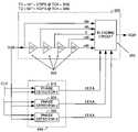
- FIG. 3is a schematic diagram of a multi-phase detector and adjustable delay circuit in accordance with one embodiment of the present invention.
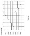
- FIG. 4is a timing diagram illustrating phase differences that may be detected in accordance with one embodiment of the present invention.
- FIG. 5is a flow chart of exemplary operations in accordance with one embodiment of the present invention.
- Embodiments of the present inventiongenerally determine, at a device (e.g., a DRAM device), a phase difference between two signals such as a clock signal (CLK) and a data strobe signal (DQS), and adjusts some parameters of timing based on the measured difference.
- a devicee.g., a DRAM device
- CLKclock signal
- DQSdata strobe signal
- the adjustmentis made to the data strobe signal itself (DQS).
- the adjustmentis made to other internal memory signals that are, perhaps, utilized in circuits controlled by the DQS signal (e.g., these signals are within the DQS domain).
- FIG. 2shows a system according to the present invention where the phase difference CLK and DQS signals is detected within a memory (e.g., a DRAM) device 230 .
- a memorye.g., a DRAM
- FIG. 2shows a partial schematic of a computer system, showing those components that relate to the present invention and not showing other components such as drives, monitors and networking so as to focus on the present invention.
- a processor 210is coupled to a memory controller 220 through various means known in the industry.
- a data bus, address bus and control busconnect the processor 210 to the memory controller 220 .
- the memory device 230is connected to and controlled by the memory controller 220 .
- Two timing signals (CLK and DQS), an address bus (ADDR), and data bus (DQ)are shown emanating from the memory controller 220 and terminating at the memory 230 .
- the memory controllersupplies the CLK and DQS signals to the memory device 230 when performing write operations to write data to memory elements 232 .
- other signals going between the memory 230 and the memory controller 220are not shown, such as control signals.
- the timing relationship (phase difference) between CLK and DQSis detected by a multi-phase detector 240 within memory 230 .
- This phase detectormay comprise multiple discrete phase detectors and may output multiple signals indicating which signal leads and the absolute value of the detected phase difference.
- n outputsare generated by the multi-phase detector 240 and these n outputs are used to control an adjustable delay circuit 250 .
- the adjustable delay circuit 250takes as input the phase difference from the phase detector 240 and the DQS signal and inserts/removes adjustable delay amounts to create an adjusted internal DQS signal (DQS′) which is then used within the memory 230 to control the timing of various circuits.
- DQS′adjusted internal DQS signal
- DQS′may be used to strobe a DATA first-in first-out (FIFO) and driver logic 270 during write operations. Further, as illustrated, DQS′ may be used to latch a word order address (WODD) on a falling edge of DQS′ that is used to order (even/odd) data received (in data receive and latch logic 275 on rising and falling edges of the DQS clock signal) within the DATA FIFO logic 270 . WODD may be latched with column address latch and counter logic 237 (that receives an address from an address receiver 235 ) in conjunction with CLK.
- WODDword order address
- DQS′may also be used to synchronize data path logic within the DATA FIFO and Driver logic 270 to drive the data received on both rising and falling edges after a serial to parallel conversion.
- the column address latch and counter 237may supply the latched addresses (WODD) to DATA FIFO and Driver logic 270 .
- WODDlatched addresses
- the adjustable delay circuit 250may include any suitable circuitry to adjust the phase of the externally supplied DQS to generate the adjusted internal DQS signal DQS′ based on the phase difference signals provided by the multi-phase detector 240 .
- the adjustable delay circuit 250including a multi-tap array of delay elements 252 , that feed a plurality of delayed versions of DQS evenly spaced in phase (e.g., every 1/8 clock cycle or 45°) into a phase blender circuit 370 .
- the phase blender circuit 370blends one or more of the delayed signals, based on the signals provided by the multi-phase detector 240 , to generate the adjusted internal DQS signal DQS′.
- the blender circuit 370allows for finer delay increments than the delay elements 252 .
- the multi-phase detector 240may include three individual phase detectors: phase detector 1 310 , phase detector 2 320 , and phase detector 3 330 .
- the output of each phase detector( 310 , 320 and 330 ) is used by the phase blender 370 to select in the delayed signals to blend to generate DQS′.
- the phase detectors 310 – 330may be designed to detect and generate different output signals (e.g., LE/LA signals illustrated in FIG. 3 ) based on different magnitudes of phase delay between DQS and CLK.
- the operating range of the phase detector and compensation in the adjustable delay circuitmay be expressed in terms of the maximum DQS ⁇ CLK timing offset, for example, with a tDQSSmin/max of 0.25*tCK (e.g., 90° out of phase) at high operation frequency (tCK> ⁇ 3 ns). At lower operation frequency the internal timing may not be as critical and the timing adjustment may be limited to the maximum adjustable delay.
- phase detector 1 310may generate a high output (e.g., logic 1) if DQS leads CLK by more than 45° and a low output (e.g., logic 0) otherwise.
- Phase detector 2 320may generate a low output if DQS leads CLK at all (e.g., by more than 0°) and a high output otherwise, while phase detector 3 330 may generate a high output if DQS lags CLK by more than 45° and a low output otherwise.
- the output signals from these phase detectorsmay be used to indicate the phase relationship between DQS and CLK by various ranges. For example, TABLE I below shows how the combined outputs of the individual phase detectors (labeled ⁇ 1 , ⁇ 2 , and ⁇ 3 ) may be interpreted.
- the blending circuit 370may then use these signals to select the delayed signals to blend in order to generate DQS′. For example, if the signals indicate DQS leads CLK by 45° or more, the blending circuit 370 may select delayed signals that result in DQS′ having significant delay relative to DQS. On the other hand, if the signals indicate DQS lags CLK by 45° or more, the blending circuit 370 may pass DQS through with minimal or no additional delay. Those skilled in the art will recognize that any number of phase detectors may be utilized to detect different ranges of phase differences between CLK and DQS.
- FIG. 4shows six different phase differences between CLK and DQS that could be detected using six phase detectors (with DQS signals DQSa–f leading/lagging by up to three unit delay periods). Output signals from six different phase detectors may be provided to the phase blender circuit to give fine resolution control to generate DQS′ that is more closely in phase with CLK.
- FIG. 5shows a flow diagram of exemplary operations that illustrates how the multi-phase detector 240 and adjustable delay circuit 250 work together to adjust internal timing of a memory device.
- the operationsbegin at step 502 by detecting (e.g., by multi-phase detector 240 ) a phase difference between externally supplied CLK and DQS signals.
- detectinge.g., by multi-phase detector 240
- an n-bit output signal indicative of the detected phase differenceis generated.
- this output signalis used to control an adjustable delay circuit to generate an internal DQS signal (DQS′ ) that is more closely in phase with the external clock signal.
- DQS′internal DQS signal
- the internal DQS signalmay be used to control the timing of circuits involving other signals, such as data and/or address signals.
- the timing of these other signalsmay also be delayed to the same effect. However, this may involve multiple delay circuits, considering the multiple other signals, and may require more complicated circuitry than delaying a single DQS signal.
Landscapes
- Engineering & Computer Science (AREA)
- Computer Networks & Wireless Communication (AREA)
- Signal Processing (AREA)
- Microelectronics & Electronic Packaging (AREA)
- Computer Hardware Design (AREA)
- Computer Security & Cryptography (AREA)
- Dram (AREA)
Abstract
Description
| TABLE I |
| Phase ranges indicated by multi-phase detector. |
| PHASE RELATIONSHIP | Ø1 | Ø2 | Ø3 | ||
| DQS leads CLK by 45° or more | 0 | 0 | 0 | ||
| DQS leads CLK by 0°–45° | 1 | 0 | 0 | ||
| DQS lags CLK by 0°–45° | 1 | 1 | 0 | ||
| DQS leads CLK by 45° or more | 1 | 1 | 1 | ||
Claims (14)
Priority Applications (4)
| Application Number | Priority Date | Filing Date | Title |
|---|---|---|---|
| US11/068,582US7209396B2 (en) | 2005-02-28 | 2005-02-28 | Data strobe synchronization for DRAM devices |
| DE102006009216ADE102006009216B4 (en) | 2005-02-28 | 2006-02-28 | Synchronization of data acknowledgment signals for DRAM devices |
| CNA2006100794247ACN1855302A (en) | 2005-02-28 | 2006-02-28 | Data strobe synchronization for dram devices |
| KR1020060019346AKR100767826B1 (en) | 2005-02-28 | 2006-02-28 | Data strobe synchronization for ???? devices |
Applications Claiming Priority (1)
| Application Number | Priority Date | Filing Date | Title |
|---|---|---|---|
| US11/068,582US7209396B2 (en) | 2005-02-28 | 2005-02-28 | Data strobe synchronization for DRAM devices |
Publications (2)
| Publication Number | Publication Date |
|---|---|
| US20060193194A1 US20060193194A1 (en) | 2006-08-31 |
| US7209396B2true US7209396B2 (en) | 2007-04-24 |
Family
ID=36848328
Family Applications (1)
| Application Number | Title | Priority Date | Filing Date |
|---|---|---|---|
| US11/068,582Expired - LifetimeUS7209396B2 (en) | 2005-02-28 | 2005-02-28 | Data strobe synchronization for DRAM devices |
Country Status (4)
| Country | Link |
|---|---|
| US (1) | US7209396B2 (en) |
| KR (1) | KR100767826B1 (en) |
| CN (1) | CN1855302A (en) |
| DE (1) | DE102006009216B4 (en) |
Cited By (35)
| Publication number | Priority date | Publication date | Assignee | Title |
|---|---|---|---|---|
| US20070008791A1 (en)* | 2005-07-07 | 2007-01-11 | Lsi Logic Corporation | DQS strobe centering (data eye training) method |
| US20080056029A1 (en)* | 2006-09-06 | 2008-03-06 | Wen-Chang Cheng | Memory control circuit and method |
| US20090168547A1 (en)* | 2007-12-28 | 2009-07-02 | Hynix Semiconductor, Inc. | Apparatus and methods for a data input circuit for a semiconductor memory apparatus |
| US20090251181A1 (en)* | 2008-04-08 | 2009-10-08 | Bae Seung Jun | Method and apparatus for tuning phase of clock signal |
| US20100329045A1 (en)* | 2009-06-24 | 2010-12-30 | Advanced Micro Devices, Inc. | Adjustment of Write Timing in a Memory Device |
| US20110047402A1 (en)* | 2003-01-30 | 2011-02-24 | Juniper Networks, Inc. | Dynamic programmable delay selection circuit and method |
| US20110228625A1 (en)* | 2009-04-01 | 2011-09-22 | Venkatraghavan Bringivijayaraghavan | Write command and write data timing circuit and methods for timing the same |
| US8300464B2 (en) | 2010-04-13 | 2012-10-30 | Freescale Semiconductor, Inc. | Method and circuit for calibrating data capture in a memory controller |
| US8509011B2 (en) | 2011-04-25 | 2013-08-13 | Micron Technology, Inc. | Command paths, apparatuses, memories, and methods for providing internal commands to a data path |
| US8552776B2 (en) | 2012-02-01 | 2013-10-08 | Micron Technology, Inc. | Apparatuses and methods for altering a forward path delay of a signal path |
| US8913448B2 (en) | 2012-10-25 | 2014-12-16 | Micron Technology, Inc. | Apparatuses and methods for capturing data in a memory |
| US8984320B2 (en) | 2011-03-29 | 2015-03-17 | Micron Technology, Inc. | Command paths, apparatuses and methods for providing a command to a data block |
| US8988966B2 (en) | 2007-03-15 | 2015-03-24 | Micron Technology, Inc. | Circuit, system and method for controlling read latency |
| US9001594B2 (en) | 2012-07-06 | 2015-04-07 | Micron Technology, Inc. | Apparatuses and methods for adjusting a path delay of a command path |
| US9025399B1 (en)* | 2013-12-06 | 2015-05-05 | Intel Corporation | Method for training a control signal based on a strobe signal in a memory module |
| US9054675B2 (en) | 2012-06-22 | 2015-06-09 | Micron Technology, Inc. | Apparatuses and methods for adjusting a minimum forward path delay of a signal path |
| US9111599B1 (en)* | 2014-06-10 | 2015-08-18 | Nanya Technology Corporation | Memory device |
| US20150256184A1 (en)* | 2014-03-05 | 2015-09-10 | SK Hynix Inc. | Semiconductor apparatus and semiconductor system including the same, and method of operating the same |
| US20150256183A1 (en)* | 2014-03-05 | 2015-09-10 | SK Hynix Inc. | Semiconductor device and semiconductor system including the same |
| US9166579B2 (en) | 2012-06-01 | 2015-10-20 | Micron Technology, Inc. | Methods and apparatuses for shifting data signals to match command signal delay |
| US9183904B2 (en) | 2014-02-07 | 2015-11-10 | Micron Technology, Inc. | Apparatuses, memories, and methods for facilitating splitting of internal commands using a shared signal path |
| US9329623B2 (en) | 2012-08-22 | 2016-05-03 | Micron Technology, Inc. | Apparatuses, integrated circuits, and methods for synchronizing data signals with a command signal |
| US9508417B2 (en) | 2014-02-20 | 2016-11-29 | Micron Technology, Inc. | Methods and apparatuses for controlling timing paths and latency based on a loop delay |
| US9531363B2 (en) | 2015-04-28 | 2016-12-27 | Micron Technology, Inc. | Methods and apparatuses including command latency control circuit |
| US9529379B2 (en) | 2006-12-19 | 2016-12-27 | Micron Technology, Inc. | Timing synchronization circuit with loop counter |
| US9530473B2 (en) | 2014-05-22 | 2016-12-27 | Micron Technology, Inc. | Apparatuses and methods for timing provision of a command to input circuitry |
| US9601170B1 (en) | 2016-04-26 | 2017-03-21 | Micron Technology, Inc. | Apparatuses and methods for adjusting a delay of a command signal path |
| US9734097B2 (en) | 2013-03-15 | 2017-08-15 | Micron Technology, Inc. | Apparatuses and methods for variable latency memory operations |
| US9813067B2 (en) | 2015-06-10 | 2017-11-07 | Micron Technology, Inc. | Clock signal and supply voltage variation tracking |
| US9865317B2 (en) | 2016-04-26 | 2018-01-09 | Micron Technology, Inc. | Methods and apparatuses including command delay adjustment circuit |
| US9997220B2 (en) | 2016-08-22 | 2018-06-12 | Micron Technology, Inc. | Apparatuses and methods for adjusting delay of command signal path |
| US10224938B2 (en) | 2017-07-26 | 2019-03-05 | Micron Technology, Inc. | Apparatuses and methods for indirectly detecting phase variations |
| US10530367B2 (en)* | 2018-12-28 | 2020-01-07 | Intel Corporation | Clock synchronization in multi-die field programmable gate array devices |
| US10860482B2 (en) | 2013-08-14 | 2020-12-08 | Micron Technology, Inc. | Apparatuses and methods for providing data to a configurable storage area |
| US11962310B1 (en) | 2022-09-14 | 2024-04-16 | Apple Inc. | Synchronization between data and clock signals in high-speed interfaces |
Families Citing this family (8)
| Publication number | Priority date | Publication date | Assignee | Title |
|---|---|---|---|---|
| US8121237B2 (en)* | 2006-03-16 | 2012-02-21 | Rambus Inc. | Signaling system with adaptive timing calibration |
| US7558132B2 (en)* | 2007-03-30 | 2009-07-07 | International Business Machines Corporation | Implementing calibration of DQS sampling during synchronous DRAM reads |
| KR100930401B1 (en)* | 2007-10-09 | 2009-12-08 | 주식회사 하이닉스반도체 | Semiconductor memory device |
| EP2232493B1 (en)* | 2007-12-21 | 2018-05-09 | Rambus Inc. | Method and apparatus for calibrating write timing in a memory system |
| US8824223B2 (en)* | 2008-02-05 | 2014-09-02 | SK Hynix Inc. | Semiconductor memory apparatus with clock and data strobe phase detection |
| US8121219B1 (en)* | 2008-02-06 | 2012-02-21 | Link—A—Media Devices Corporation | Decision directed timing recovery using multiphase detection |
| CN102610268B (en)* | 2012-01-10 | 2014-04-02 | 江苏中科梦兰电子科技有限公司 | Method for synchronizing data strobe signal in double data rate 3(DDR3) using oscilloscope |
| CN111010181B (en)* | 2019-12-19 | 2023-11-10 | 深圳市联洲国际技术有限公司 | DDR signal time sequence calibration method and device |
Citations (3)
| Publication number | Priority date | Publication date | Assignee | Title |
|---|---|---|---|---|
| KR20000018490A (en) | 1998-09-02 | 2000-04-06 | 윤종용 | Delay synchronization loop equipped with controller for varying unit delay device number of voltage control delay line and method thereof |
| US20030086303A1 (en)* | 2001-11-06 | 2003-05-08 | Samsung Electronics Co., Ltd. | Data input circuits and methods of inputing data for a synchronous semiconductor memory device |
| US20040222828A1 (en)* | 2002-10-25 | 2004-11-11 | Elpida Memory, Inc. | Timing adjustment circuit and semiconductor device including the same |
Family Cites Families (6)
| Publication number | Priority date | Publication date | Assignee | Title |
|---|---|---|---|---|
| US6570944B2 (en)* | 2001-06-25 | 2003-05-27 | Rambus Inc. | Apparatus for data recovery in a synchronous chip-to-chip system |
| US5056054A (en) | 1990-05-02 | 1991-10-08 | National Semiconductor Corporation | Digital phase locked loop utilizing a multi-bit phase error input for control of a stepped clock generator |
| US5224125A (en) | 1991-04-05 | 1993-06-29 | National Semiconductor Corporation | Digital signed phase-to-frequency converter for very high frequency phase locked loops |
| JPH08162913A (en)* | 1994-12-08 | 1996-06-21 | Nippon Telegr & Teleph Corp <Ntt> | Direct logic synthesis signal generator |
| JP3961072B2 (en) | 1997-06-12 | 2007-08-15 | 富士通株式会社 | Semiconductor device and timing adjustment method thereof |
| US6140854A (en)* | 1999-01-25 | 2000-10-31 | Motorola, Inc. | System with DLL |
- 2005
- 2005-02-28USUS11/068,582patent/US7209396B2/ennot_activeExpired - Lifetime
- 2006
- 2006-02-28KRKR1020060019346Apatent/KR100767826B1/ennot_activeExpired - Fee Related
- 2006-02-28CNCNA2006100794247Apatent/CN1855302A/enactivePending
- 2006-02-28DEDE102006009216Apatent/DE102006009216B4/ennot_activeExpired - Fee Related
Patent Citations (5)
| Publication number | Priority date | Publication date | Assignee | Title |
|---|---|---|---|---|
| KR20000018490A (en) | 1998-09-02 | 2000-04-06 | 윤종용 | Delay synchronization loop equipped with controller for varying unit delay device number of voltage control delay line and method thereof |
| US6329854B1 (en)* | 1998-09-02 | 2001-12-11 | Samsung Electronics Co., Ltd. | Phase locked loop integrated circuits having dynamic phase locking characteristics and methods of operating same |
| US20030086303A1 (en)* | 2001-11-06 | 2003-05-08 | Samsung Electronics Co., Ltd. | Data input circuits and methods of inputing data for a synchronous semiconductor memory device |
| KR20030037588A (en) | 2001-11-06 | 2003-05-14 | 삼성전자주식회사 | Data input circuit and data input method for synchronous semiconductor memory device |
| US20040222828A1 (en)* | 2002-10-25 | 2004-11-11 | Elpida Memory, Inc. | Timing adjustment circuit and semiconductor device including the same |
Non-Patent Citations (1)
| Title |
|---|
| KIPO Examination Report dated Dec. 15, 2006. |
Cited By (64)
| Publication number | Priority date | Publication date | Assignee | Title |
|---|---|---|---|---|
| US8082463B2 (en)* | 2003-01-30 | 2011-12-20 | Juniper Networks, Inc. | Dynamic programmable delay selection circuit and method |
| US20110047402A1 (en)* | 2003-01-30 | 2011-02-24 | Juniper Networks, Inc. | Dynamic programmable delay selection circuit and method |
| US7443741B2 (en)* | 2005-07-07 | 2008-10-28 | Lsi Corporation | DQS strobe centering (data eye training) method |
| US20070008791A1 (en)* | 2005-07-07 | 2007-01-11 | Lsi Logic Corporation | DQS strobe centering (data eye training) method |
| US20080056029A1 (en)* | 2006-09-06 | 2008-03-06 | Wen-Chang Cheng | Memory control circuit and method |
| US7580301B2 (en)* | 2006-09-06 | 2009-08-25 | Nanya Technology Corp. | Method control circuit performing adjustable data delay operation based upon phase difference between data strobe signal and clock signal, and associated method |
| US9529379B2 (en) | 2006-12-19 | 2016-12-27 | Micron Technology, Inc. | Timing synchronization circuit with loop counter |
| US8988966B2 (en) | 2007-03-15 | 2015-03-24 | Micron Technology, Inc. | Circuit, system and method for controlling read latency |
| US10658019B2 (en) | 2007-03-15 | 2020-05-19 | Micron Technology, Inc. | Circuit, system and method for controlling read latency |
| US20090168547A1 (en)* | 2007-12-28 | 2009-07-02 | Hynix Semiconductor, Inc. | Apparatus and methods for a data input circuit for a semiconductor memory apparatus |
| KR100907016B1 (en) | 2007-12-28 | 2009-07-08 | 주식회사 하이닉스반도체 | Data input circuit of semiconductor memory device and control method thereof |
| US7719904B2 (en) | 2007-12-28 | 2010-05-18 | Hynix Semiconductor Inc. | Data input circuit for a semiconductor memory capable of adapting to a phase skew between a data strobe signal and an external clock signal |
| US8242819B2 (en)* | 2008-04-08 | 2012-08-14 | Samsung Electronics Co., Ltd. | Method and apparatus for tuning phase of clock signal |
| US20110158030A1 (en)* | 2008-04-08 | 2011-06-30 | Samsung Electronics Co., Ltd. | Method and apparatus for tuning phase of clock signal |
| US20090251181A1 (en)* | 2008-04-08 | 2009-10-08 | Bae Seung Jun | Method and apparatus for tuning phase of clock signal |
| KR101499176B1 (en)* | 2008-04-08 | 2015-03-06 | 삼성전자주식회사 | Method and apparatus for phase tuning of clock signal |
| US7902887B2 (en)* | 2008-04-08 | 2011-03-08 | Samsung Electronics Co., Ltd. | Method and apparatus for tuning phase of clock signal |
| US20110228625A1 (en)* | 2009-04-01 | 2011-09-22 | Venkatraghavan Bringivijayaraghavan | Write command and write data timing circuit and methods for timing the same |
| US8441888B2 (en) | 2009-04-01 | 2013-05-14 | Micron Technology, Inc. | Write command and write data timing circuit and methods for timing the same |
| US8760961B2 (en) | 2009-04-01 | 2014-06-24 | Micron Technology, Inc. | Write command and write data timing circuit and methods for timing the same |
| US8730758B2 (en)* | 2009-06-24 | 2014-05-20 | Advanced Micro Devices, Inc. | Adjustment of write timing in a memory device |
| US9508408B2 (en) | 2009-06-24 | 2016-11-29 | Advanced Micro Devices, Inc. | Adjustment of write timing in a memory device |
| KR20160003323A (en)* | 2009-06-24 | 2016-01-08 | 어드밴스드 마이크로 디바이시즈, 인코포레이티드 | Adjustment of write timing in a memory device |
| KR101580659B1 (en) | 2009-06-24 | 2015-12-28 | 어드밴스드 마이크로 디바이시즈, 인코포레이티드 | Adjustment of write timing in a memory device |
| US20100329045A1 (en)* | 2009-06-24 | 2010-12-30 | Advanced Micro Devices, Inc. | Adjustment of Write Timing in a Memory Device |
| KR101710151B1 (en) | 2009-06-24 | 2017-02-24 | 어드밴스드 마이크로 디바이시즈, 인코포레이티드 | Adjustment of write timing in a memory device |
| KR20120106699A (en)* | 2009-06-24 | 2012-09-26 | 어드밴스드 마이크로 디바이시즈, 인코포레이티드 | Adjustment of write timing in a memory device |
| US8300464B2 (en) | 2010-04-13 | 2012-10-30 | Freescale Semiconductor, Inc. | Method and circuit for calibrating data capture in a memory controller |
| US8984320B2 (en) | 2011-03-29 | 2015-03-17 | Micron Technology, Inc. | Command paths, apparatuses and methods for providing a command to a data block |
| US8644096B2 (en) | 2011-04-25 | 2014-02-04 | Micron Technology, Inc. | Command paths, apparatuses, memories, and methods for providing internal commands to a data path |
| US8509011B2 (en) | 2011-04-25 | 2013-08-13 | Micron Technology, Inc. | Command paths, apparatuses, memories, and methods for providing internal commands to a data path |
| US9000817B2 (en) | 2012-02-01 | 2015-04-07 | Micron Technology, Inc. | Apparatuses and methods for altering a forward path delay of a signal path |
| US8552776B2 (en) | 2012-02-01 | 2013-10-08 | Micron Technology, Inc. | Apparatuses and methods for altering a forward path delay of a signal path |
| US9166579B2 (en) | 2012-06-01 | 2015-10-20 | Micron Technology, Inc. | Methods and apparatuses for shifting data signals to match command signal delay |
| US9054675B2 (en) | 2012-06-22 | 2015-06-09 | Micron Technology, Inc. | Apparatuses and methods for adjusting a minimum forward path delay of a signal path |
| US9001594B2 (en) | 2012-07-06 | 2015-04-07 | Micron Technology, Inc. | Apparatuses and methods for adjusting a path delay of a command path |
| US9329623B2 (en) | 2012-08-22 | 2016-05-03 | Micron Technology, Inc. | Apparatuses, integrated circuits, and methods for synchronizing data signals with a command signal |
| US8913448B2 (en) | 2012-10-25 | 2014-12-16 | Micron Technology, Inc. | Apparatuses and methods for capturing data in a memory |
| US10740263B2 (en) | 2013-03-15 | 2020-08-11 | Micron Technology, Inc. | Apparatuses and methods for variable latency memory operations |
| US9734097B2 (en) | 2013-03-15 | 2017-08-15 | Micron Technology, Inc. | Apparatuses and methods for variable latency memory operations |
| US10860482B2 (en) | 2013-08-14 | 2020-12-08 | Micron Technology, Inc. | Apparatuses and methods for providing data to a configurable storage area |
| US9627029B2 (en) | 2013-12-06 | 2017-04-18 | Intel Corporation | Method for training a control signal based on a strobe signal in a memory module |
| US9025399B1 (en)* | 2013-12-06 | 2015-05-05 | Intel Corporation | Method for training a control signal based on a strobe signal in a memory module |
| US9183904B2 (en) | 2014-02-07 | 2015-11-10 | Micron Technology, Inc. | Apparatuses, memories, and methods for facilitating splitting of internal commands using a shared signal path |
| US9508417B2 (en) | 2014-02-20 | 2016-11-29 | Micron Technology, Inc. | Methods and apparatuses for controlling timing paths and latency based on a loop delay |
| US20150256184A1 (en)* | 2014-03-05 | 2015-09-10 | SK Hynix Inc. | Semiconductor apparatus and semiconductor system including the same, and method of operating the same |
| US9374096B2 (en)* | 2014-03-05 | 2016-06-21 | SK Hynix Inc. | Semiconductor apparatus and semiconductor system including the same, and method of operating the same |
| US9191010B2 (en)* | 2014-03-05 | 2015-11-17 | SK Hynix Inc. | Semiconductor device and semiconductor system including the same |
| US20150256183A1 (en)* | 2014-03-05 | 2015-09-10 | SK Hynix Inc. | Semiconductor device and semiconductor system including the same |
| US9530473B2 (en) | 2014-05-22 | 2016-12-27 | Micron Technology, Inc. | Apparatuses and methods for timing provision of a command to input circuitry |
| US9111599B1 (en)* | 2014-06-10 | 2015-08-18 | Nanya Technology Corporation | Memory device |
| US9531363B2 (en) | 2015-04-28 | 2016-12-27 | Micron Technology, Inc. | Methods and apparatuses including command latency control circuit |
| US9813067B2 (en) | 2015-06-10 | 2017-11-07 | Micron Technology, Inc. | Clock signal and supply voltage variation tracking |
| US10193558B2 (en) | 2015-06-10 | 2019-01-29 | Micron Technology, Inc. | Clock signal and supply voltage variation tracking |
| US9601170B1 (en) | 2016-04-26 | 2017-03-21 | Micron Technology, Inc. | Apparatuses and methods for adjusting a delay of a command signal path |
| US10290336B2 (en) | 2016-04-26 | 2019-05-14 | Micron Technology, Inc. | Methods and apparatuses including command delay adjustment circuit |
| US10755758B2 (en) | 2016-04-26 | 2020-08-25 | Micron Technology, Inc. | Methods and apparatuses including command delay adjustment circuit |
| US9865317B2 (en) | 2016-04-26 | 2018-01-09 | Micron Technology, Inc. | Methods and apparatuses including command delay adjustment circuit |
| US9997220B2 (en) | 2016-08-22 | 2018-06-12 | Micron Technology, Inc. | Apparatuses and methods for adjusting delay of command signal path |
| US11087806B2 (en) | 2016-08-22 | 2021-08-10 | Micron Technology, Inc. | Apparatuses and methods for adjusting delay of command signal path |
| US10224938B2 (en) | 2017-07-26 | 2019-03-05 | Micron Technology, Inc. | Apparatuses and methods for indirectly detecting phase variations |
| US10797708B2 (en) | 2017-07-26 | 2020-10-06 | Micron Technology, Inc. | Apparatuses and methods for indirectly detecting phase variations |
| US10530367B2 (en)* | 2018-12-28 | 2020-01-07 | Intel Corporation | Clock synchronization in multi-die field programmable gate array devices |
| US11962310B1 (en) | 2022-09-14 | 2024-04-16 | Apple Inc. | Synchronization between data and clock signals in high-speed interfaces |
Also Published As
| Publication number | Publication date |
|---|---|
| US20060193194A1 (en) | 2006-08-31 |
| KR100767826B1 (en) | 2007-10-18 |
| DE102006009216A1 (en) | 2006-09-07 |
| CN1855302A (en) | 2006-11-01 |
| DE102006009216B4 (en) | 2011-01-27 |
| KR20060095519A (en) | 2006-08-31 |
Similar Documents
| Publication | Publication Date | Title |
|---|---|---|
| US7209396B2 (en) | Data strobe synchronization for DRAM devices | |
| US7227809B2 (en) | Clock generator having a delay locked loop and duty cycle correction circuit in a parallel configuration | |
| US7266022B2 (en) | Memory interface control circuit | |
| US6836166B2 (en) | Method and system for delay control in synchronization circuits | |
| KR100813554B1 (en) | Data output strobe signal generation circuit and semiconductor memory device including the same | |
| US9472255B2 (en) | Semiconductor device including a clock generating circuit for generating an internal signal having a coarse delay line, a fine delay line and a selector circuit | |
| US8115529B2 (en) | Device and control method of device | |
| US7385861B1 (en) | Synchronization circuit for DDR IO interface | |
| KR101685630B1 (en) | DLL having 2-phase delay line and duty correction circuit and duty correction method thereof | |
| US7596043B2 (en) | Delay locked loop circuit for a synchronous semiconductor memory device and a method of generating information about a load connected to a data pin of a synchronous semiconductor memory device | |
| US7764554B2 (en) | I/O circuit with phase mixer for slew rate control | |
| US20100103746A1 (en) | Multi-phase duty-cycle corrected clock signal generator and memory having same | |
| KR100722775B1 (en) | Delay Synchronous Loop Circuit and Delay Synchronous Loop Control Method of Semiconductor Device | |
| US8306169B2 (en) | Semiconductor devices, methods of operating semiconductor devices, and systems having the same | |
| US7298189B2 (en) | Delay locked loop circuit | |
| US20080061851A1 (en) | Delay locked loop circuit capable of reducing bang-bang jitter | |
| US20090278580A1 (en) | Clock control circuit and a semiconductor memory apparatus having the same | |
| KR100843002B1 (en) | Duty Cycle Compensation Circuit and Delay-Locked Loop With It | |
| US6996026B2 (en) | Devices for synchronizing clock signals | |
| US8134391B2 (en) | Semiconductor devices with signal synchronization circuits | |
| US6467043B1 (en) | Adjusting and measuring the timing of a data strobe signal with a first delay line and through additional delay line adapted to receive pulse signal | |
| US7405996B2 (en) | System and method to synchronize signals in individual integrated circuit components | |
| US7068567B2 (en) | Data output controller in semiconductor memory device and control method thereof | |
| US8169842B2 (en) | Skew detector and semiconductor memory device using the same | |
| US20070205817A1 (en) | Method, circuit and system for detecting a locked state of a clock synchronization circuit |
Legal Events
| Date | Code | Title | Description |
|---|---|---|---|
| AS | Assignment | Owner name:INFINEON TECHNOLOGIES NORTH AMERICA CORP., CALIFOR Free format text:ASSIGNMENT OF ASSIGNORS INTEREST;ASSIGNOR:SCHNELL, JOSEF;REEL/FRAME:015791/0274 Effective date:20050225 | |
| AS | Assignment | Owner name:INFINEON TECHNOLOGIES AG, GERMANY Free format text:ASSIGNMENT OF ASSIGNORS INTEREST;ASSIGNOR:INFINEON TECHNOLOGIES NORTH AMERICA CORP.;REEL/FRAME:015799/0306 Effective date:20050317 | |
| STCF | Information on status: patent grant | Free format text:PATENTED CASE | |
| AS | Assignment | Owner name:QIMONDA AG, GERMANY Free format text:ASSIGNMENT OF ASSIGNORS INTEREST;ASSIGNOR:INFINEON TECHNOLOGIES AG;REEL/FRAME:023806/0001 Effective date:20060425 Owner name:QIMONDA AG,GERMANY Free format text:ASSIGNMENT OF ASSIGNORS INTEREST;ASSIGNOR:INFINEON TECHNOLOGIES AG;REEL/FRAME:023806/0001 Effective date:20060425 | |
| FPAY | Fee payment | Year of fee payment:4 | |
| FPAY | Fee payment | Year of fee payment:8 | |
| AS | Assignment | Owner name:INFINEON TECHNOLOGIES AG, GERMANY Free format text:ASSIGNMENT OF ASSIGNORS INTEREST;ASSIGNOR:QIMONDA AG;REEL/FRAME:035623/0001 Effective date:20141009 | |
| AS | Assignment | Owner name:POLARIS INNOVATIONS LIMITED, IRELAND Free format text:ASSIGNMENT OF ASSIGNORS INTEREST;ASSIGNOR:INFINEON TECHNOLOGIES AG;REEL/FRAME:036908/0923 Effective date:20150708 | |
| MAFP | Maintenance fee payment | Free format text:PAYMENT OF MAINTENANCE FEE, 12TH YEAR, LARGE ENTITY (ORIGINAL EVENT CODE: M1553); ENTITY STATUS OF PATENT OWNER: LARGE ENTITY Year of fee payment:12 |