US7205970B2 - Liquid crystal display for wide viewing angle, and driving method thereof - Google Patents
Liquid crystal display for wide viewing angle, and driving method thereofDownload PDFInfo
- Publication number
- US7205970B2 US7205970B2US10/233,869US23386902AUS7205970B2US 7205970 B2US7205970 B2US 7205970B2US 23386902 AUS23386902 AUS 23386902AUS 7205970 B2US7205970 B2US 7205970B2
- Authority
- US
- United States
- Prior art keywords
- gray level
- data
- level data
- liquid crystal
- crystal display
- Prior art date
- Legal status (The legal status is an assumption and is not a legal conclusion. Google has not performed a legal analysis and makes no representation as to the accuracy of the status listed.)
- Expired - Fee Related, expires
Links
Images


Classifications
- G—PHYSICS
- G02—OPTICS
- G02F—OPTICAL DEVICES OR ARRANGEMENTS FOR THE CONTROL OF LIGHT BY MODIFICATION OF THE OPTICAL PROPERTIES OF THE MEDIA OF THE ELEMENTS INVOLVED THEREIN; NON-LINEAR OPTICS; FREQUENCY-CHANGING OF LIGHT; OPTICAL LOGIC ELEMENTS; OPTICAL ANALOGUE/DIGITAL CONVERTERS
- G02F1/00—Devices or arrangements for the control of the intensity, colour, phase, polarisation or direction of light arriving from an independent light source, e.g. switching, gating or modulating; Non-linear optics
- G02F1/01—Devices or arrangements for the control of the intensity, colour, phase, polarisation or direction of light arriving from an independent light source, e.g. switching, gating or modulating; Non-linear optics for the control of the intensity, phase, polarisation or colour
- G02F1/13—Devices or arrangements for the control of the intensity, colour, phase, polarisation or direction of light arriving from an independent light source, e.g. switching, gating or modulating; Non-linear optics for the control of the intensity, phase, polarisation or colour based on liquid crystals, e.g. single liquid crystal display cells
- G02F1/133—Constructional arrangements; Operation of liquid crystal cells; Circuit arrangements
- G—PHYSICS
- G09—EDUCATION; CRYPTOGRAPHY; DISPLAY; ADVERTISING; SEALS
- G09G—ARRANGEMENTS OR CIRCUITS FOR CONTROL OF INDICATING DEVICES USING STATIC MEANS TO PRESENT VARIABLE INFORMATION
- G09G5/00—Control arrangements or circuits for visual indicators common to cathode-ray tube indicators and other visual indicators
- G09G5/003—Details of a display terminal, the details relating to the control arrangement of the display terminal and to the interfaces thereto
- G09G5/005—Adapting incoming signals to the display format of the display terminal
- G—PHYSICS
- G09—EDUCATION; CRYPTOGRAPHY; DISPLAY; ADVERTISING; SEALS
- G09G—ARRANGEMENTS OR CIRCUITS FOR CONTROL OF INDICATING DEVICES USING STATIC MEANS TO PRESENT VARIABLE INFORMATION
- G09G3/00—Control arrangements or circuits, of interest only in connection with visual indicators other than cathode-ray tubes
- G09G3/20—Control arrangements or circuits, of interest only in connection with visual indicators other than cathode-ray tubes for presentation of an assembly of a number of characters, e.g. a page, by composing the assembly by combination of individual elements arranged in a matrix no fixed position being assigned to or needed to be assigned to the individual characters or partial characters
- G09G3/34—Control arrangements or circuits, of interest only in connection with visual indicators other than cathode-ray tubes for presentation of an assembly of a number of characters, e.g. a page, by composing the assembly by combination of individual elements arranged in a matrix no fixed position being assigned to or needed to be assigned to the individual characters or partial characters by control of light from an independent source
- G09G3/36—Control arrangements or circuits, of interest only in connection with visual indicators other than cathode-ray tubes for presentation of an assembly of a number of characters, e.g. a page, by composing the assembly by combination of individual elements arranged in a matrix no fixed position being assigned to or needed to be assigned to the individual characters or partial characters by control of light from an independent source using liquid crystals
- G09G3/3611—Control of matrices with row and column drivers
- G09G3/3622—Control of matrices with row and column drivers using a passive matrix
- G09G3/3629—Control of matrices with row and column drivers using a passive matrix using liquid crystals having memory effects, e.g. ferroelectric liquid crystals
- G—PHYSICS
- G09—EDUCATION; CRYPTOGRAPHY; DISPLAY; ADVERTISING; SEALS
- G09G—ARRANGEMENTS OR CIRCUITS FOR CONTROL OF INDICATING DEVICES USING STATIC MEANS TO PRESENT VARIABLE INFORMATION
- G09G2320/00—Control of display operating conditions
- G09G2320/02—Improving the quality of display appearance
- G09G2320/0247—Flicker reduction other than flicker reduction circuits used for single beam cathode-ray tubes
- G—PHYSICS
- G09—EDUCATION; CRYPTOGRAPHY; DISPLAY; ADVERTISING; SEALS
- G09G—ARRANGEMENTS OR CIRCUITS FOR CONTROL OF INDICATING DEVICES USING STATIC MEANS TO PRESENT VARIABLE INFORMATION
- G09G2320/00—Control of display operating conditions
- G09G2320/02—Improving the quality of display appearance
- G09G2320/0271—Adjustment of the gradation levels within the range of the gradation scale, e.g. by redistribution or clipping
- G09G2320/0276—Adjustment of the gradation levels within the range of the gradation scale, e.g. by redistribution or clipping for the purpose of adaptation to the characteristics of a display device, i.e. gamma correction
- G—PHYSICS
- G09—EDUCATION; CRYPTOGRAPHY; DISPLAY; ADVERTISING; SEALS
- G09G—ARRANGEMENTS OR CIRCUITS FOR CONTROL OF INDICATING DEVICES USING STATIC MEANS TO PRESENT VARIABLE INFORMATION
- G09G2320/00—Control of display operating conditions
- G09G2320/02—Improving the quality of display appearance
- G09G2320/028—Improving the quality of display appearance by changing the viewing angle properties, e.g. widening the viewing angle, adapting the viewing angle to the view direction
- G—PHYSICS
- G09—EDUCATION; CRYPTOGRAPHY; DISPLAY; ADVERTISING; SEALS
- G09G—ARRANGEMENTS OR CIRCUITS FOR CONTROL OF INDICATING DEVICES USING STATIC MEANS TO PRESENT VARIABLE INFORMATION
- G09G2320/00—Control of display operating conditions
- G09G2320/02—Improving the quality of display appearance
- G09G2320/0285—Improving the quality of display appearance using tables for spatial correction of display data
- G—PHYSICS
- G09—EDUCATION; CRYPTOGRAPHY; DISPLAY; ADVERTISING; SEALS
- G09G—ARRANGEMENTS OR CIRCUITS FOR CONTROL OF INDICATING DEVICES USING STATIC MEANS TO PRESENT VARIABLE INFORMATION
- G09G3/00—Control arrangements or circuits, of interest only in connection with visual indicators other than cathode-ray tubes
- G09G3/20—Control arrangements or circuits, of interest only in connection with visual indicators other than cathode-ray tubes for presentation of an assembly of a number of characters, e.g. a page, by composing the assembly by combination of individual elements arranged in a matrix no fixed position being assigned to or needed to be assigned to the individual characters or partial characters
- G09G3/2007—Display of intermediate tones
- G09G3/2044—Display of intermediate tones using dithering
- G09G3/2051—Display of intermediate tones using dithering with use of a spatial dither pattern
- G—PHYSICS
- G09—EDUCATION; CRYPTOGRAPHY; DISPLAY; ADVERTISING; SEALS
- G09G—ARRANGEMENTS OR CIRCUITS FOR CONTROL OF INDICATING DEVICES USING STATIC MEANS TO PRESENT VARIABLE INFORMATION
- G09G3/00—Control arrangements or circuits, of interest only in connection with visual indicators other than cathode-ray tubes
- G09G3/20—Control arrangements or circuits, of interest only in connection with visual indicators other than cathode-ray tubes for presentation of an assembly of a number of characters, e.g. a page, by composing the assembly by combination of individual elements arranged in a matrix no fixed position being assigned to or needed to be assigned to the individual characters or partial characters
- G09G3/34—Control arrangements or circuits, of interest only in connection with visual indicators other than cathode-ray tubes for presentation of an assembly of a number of characters, e.g. a page, by composing the assembly by combination of individual elements arranged in a matrix no fixed position being assigned to or needed to be assigned to the individual characters or partial characters by control of light from an independent source
- G09G3/36—Control arrangements or circuits, of interest only in connection with visual indicators other than cathode-ray tubes for presentation of an assembly of a number of characters, e.g. a page, by composing the assembly by combination of individual elements arranged in a matrix no fixed position being assigned to or needed to be assigned to the individual characters or partial characters by control of light from an independent source using liquid crystals
- G09G3/3611—Control of matrices with row and column drivers
- G09G3/3614—Control of polarity reversal in general
- G—PHYSICS
- G09—EDUCATION; CRYPTOGRAPHY; DISPLAY; ADVERTISING; SEALS
- G09G—ARRANGEMENTS OR CIRCUITS FOR CONTROL OF INDICATING DEVICES USING STATIC MEANS TO PRESENT VARIABLE INFORMATION
- G09G5/00—Control arrangements or circuits for visual indicators common to cathode-ray tube indicators and other visual indicators
- G09G5/003—Details of a display terminal, the details relating to the control arrangement of the display terminal and to the interfaces thereto
- G09G5/006—Details of the interface to the display terminal
Definitions
- the present inventionrelates generally to a liquid crystal display and a driving method thereof, and more particularly to a liquid crystal display for wide viewing angle for suppressing occurrence of lower gray level inversion and a driving method thereof.
- TNtwisted nematic
- LCDliquid crystal display
- liquid crystal directorsare arranged as shown in FIG. 1 .
- FIG. 1is a view of liquid crystal directors dependent on voltages applied to the liquid crystal cells.
- the transmission rateis decreased with gradual decrease of the phase retardation when the application voltage rises from V 1 to V 2 but is increased with gradual increase of the phase retardation when the application voltage rises from V 2 to V 3 .
- the transmission rateis high at a higher application voltage rather than a lower application voltage above a certain angle. This is referred to as “gray level inversion”, which will be explained with reference to FIG. 2 .
- FIG. 2illustrates a gray level indication according to a prior viewing angle.
- a normal gray levelcan be identified in the front sight of the liquid crystal panel, but an abnormal gray level may be identified in the sight from a position lower than the front.
- an abnormal gray levelmay be identified in the sight from a position lower than the front.
- Such a lower gray level inversioncauses a problem of narrow viewing angle that viewing angle of the liquid crystal display becomes narrow.
- a flickeroccurs in the liquid crystal display due to a swing of a common electrode voltage or a difference of response time of the liquid crystal.
- FIGS. 3 a and 3 billustrate a flicker caused by a swing of common electrode voltage generated in a prior liquid crystal display.
- the liquid crystal display with a normal white modewhich has white gray level in case of no application of voltage to the pixel and black gray level in case of application of voltage to the pixel, will be described as an example.
- FIG. 3 ashows pixel voltages applied to first to fourth pixels for each frame.
- FIG. 3 bshows pixel voltages actually felt by pixels, which are applied to the first to fourth pixels placed spatially in FIG. 3 a for each frame.
- FIG. 4is a diagram of a flicker caused by a difference of response time of the liquid crystal generated in a prior liquid crystal display, particularly (a) is for illustrating a voltage applied to a certain pixel for each frame (7 frames shown) and a brightness level responding to the voltage and (b) is for illustrating a voltage applied to a pixel adjacent to the certain pixel for each frame and a brightness level responding to the voltage.
- a flickeroccurs in a portion indicated by a circle in the entire screen when the pixels having two waveforms in the right and left are driven on their average.
- the inventionprovides a liquid crystal display for wide viewing angle which is capable of suppressing the occurrence of the flicker and overcoming the lower gray level inversion problem by representing brightness indicated by more than two gray level voltages as one gray level through an inversion method or a method by which brightness pattern for each frame is optimized and time-averaged.
- the inventionfurther provides a driving method of the liquid crystal display for wide viewing angle.
- a liquid crystal display for wide viewing anglecomprises,
- a timing controllerfor storing more than one gray level correction values for averaging optically brightness level corresponding to gray level data in a memory and outputting average gray level data reflecting the gray level correction value in association with input of certain gray level data from the external;
- a gate driverfor outputting sequentially a predetermined scanning signal
- a data driverfor receiving the average gray level data and transforming them into predetermined data voltages to be outputted
- a liquid crystal panelfor displaying an image according to the data voltages when the scanning signals are inputted.
- the timing controlleroutputs average gray level data generated by averaging gray level data corresponding to more than one sub-pixels of each of RGBs based on the more than one gray level correction values as the gray data corresponding to the sub pixels of each of RGBs is applied from the external.
- the timing controllerhas a signal processing unit for producing and outputting a first control signal to be inputted to the data driver, a second control signal to be inputted to the gate driver, and a third control signal to be inputted to a driving voltage generating unit; and a gray level averaging unit for outputting the average gray level data produced by averaging gray levels of image data from the external.
- a driving method of a liquid crystal displayincluding a plurality of gate line, a plurality of data lines intersecting the plurality of gate line perpendicularly, pixel electrodes formed in regions between the gate lines and the data lines, and switching devices connected to the gate lines, the data lines, and the pixel electrodes, comprises the steps of: (a) receiving gray level data for picture display from an external source of picture signals; (b) generating average gray level data reflecting gray level correction values corresponding to the gray level data; (c) converting the average gray level data into data voltages; (d) applying the data voltages to the data lines; and (e) applying sequentially scanning signals for output of the data voltages to the gate lines.
- the step of (b)includes (b- 1 ) extracting first and second gray level correction values corresponding to the gray level data from a memory; and (b- 2 ) generating the average gray level data reflecting the first and second gray level correction values.
- the first gray level correction valueis a voltage for driving the pixel electrodes at a level lower than the gray level data and the second gray level correction value is a voltage for driving the pixel electrodes at a level higher than the gray level data.
- the average gray level data in the step of (b- 2 )generates a first average gray level data by subtracting the first gray level correction value from the gray level data, the generated first average gray level data being applied when odd or even numbers of frames are driven, and a second average gray level data by subtracting the second gray level correction value from the gray level data, the generated second average gray level data being applied when odd or even number of frames are driven.
- the average gray level data in the step of (b- 2 )is the first gray level correction value corresponding to the gray level data when the odd numbers of frames are driven and the second gray level correction value corresponding to the gray level data when the even numbers of frames are driven.
- the lower gray level inversion problem in the TN modecan be overcome by representing brightness indicated by more than two gray level voltages as one gray level through an inversion method or a method by which brightness pattern for each frame is optimized and time-averaged.
- FIG. 1illustrates an array of liquid crystal directors dependent on voltages applied to the liquid crystal cell
- FIG. 2is a diagram of a gray level indication according to a prior viewing angle
- FIGS. 3A and 3Billustrate a flicker caused by a swing of common electrode voltage generated in a prior liquid crystal display
- FIG. 4illustrates a flicker caused by a difference of response time of the liquid crystal generated in a prior liquid crystal display
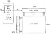
- FIG. 5is a block diagram illustrating a liquid crystal display for wide viewing angle according to an embodiment of the present invention.
- FIG. 6is a detailed view of the timing controller of FIG. 5 ;
- FIGS. 7 a and 7 billustrate averaging two gray levels according to an embodiment of the present invention
- FIG. 8shows an operation of m and m′ for a particular n on a gamma curve of FIGS. 7 a and 7 b;
- FIGS. 9 a to 9 dare graphs showing optical properties of the lower gray level inversion based on viewing angles corresponding to the values of m defined according to the present invention.
- FIG. 10is a graph for illustrating gray level display according to the present invention.
- FIGS. 11 a and 11 billustrate averaging two gray levels according to another embodiment of the present invention.
- FIG. 12is a graph showing an operation of m and m′ for a particular n on a gamma curve of FIGS. 11 a and 11 b.
- premised conditions on a method for averaging more than two gray levels using a driving method according to the present inventionare as follows.
- gray level to be averaged for each gray levelshould be calculated for same measurement as gamma curve prior to the gray level averaging.
- magnitude of positive and negative polaritiesshould be symmetrical without DC component during a constant period in one pixel.
- brightness averageshould be constant in a constant period in one pixel.
- pixels with different screen brightness due to difference of response time of liquid crystalsshould be properly averaged so that an observer cannot perceive the brightness difference.
- FIG. 5shows a liquid crystal display for wide viewing angle according to an embodiment of the present invention.
- a liquid crystal display for wide viewing angleincludes a timing controller 100 including a gray level averaging unit 110 , a gate driver 200 , a data driver 300 and a liquid crystal panel 400 .
- the timing controller 100outputs gray level data Gn′ averaged based on gray level data Gn supplied to the data driver 300 .
- the timing controller 100stores in a memory first and second gray level correction values for optically averaging a brightness level corresponding to gray level data using the inversion method or a method of optimizing and time-averaging a brightness pattern for each frame and outputs averaged gray level data Gn′ reflecting the first and second gray level correction values in association with a particular gray level input data Gn.
- the gate driver 200applies scan signals (or gate ON voltages) to the liquid crystal panel 400 based on a timing signal (not shown) from the timing controller 100 and turns on TFTs where gate electrodes are connected to gate lines to which the gate ON voltages are applied.
- the data driver 300converts averaged gray level data Gn′ from the timing controller 100 to data voltages and outputs the data voltages to the liquid crystal panel 400 .
- the liquid panel 400has a plurality of gate lines S 1 , S 2 , S 3 , . . . , Sn for transferring the gate ON signals and a plurality of data lines D 1 , D 2 , . . . , for transferring the data voltages.
- Each of regions surrounded by the gate lines and the data linesforms a pixel.
- Each of pixelincludes a thick film transistor having a gate electrode and a source electrode connected to a corresponding gate line and a corresponding data line, respectively, and a liquid capacitor Clc and a storage capacitor Cst connected in parallel to a drain electrode of the thick film transistor.
- the present inventionincludes a stand-alone gray level averaging unit separated from the timing controller.
- timing controllerincluding the gray level averaging unit will be in detail described with reference to the attached drawings.
- FIG. 6shows a detailed view of the timing controller of FIG. 5 .
- the timing controller of the present inventionincludes the gray level averaging unit 110 , an input processing unit 120 , a clock processing unit 130 and a signal processing unit 140 .
- the gray level averaging unit 110having a data processing unit 112 and a lookup table 114 further performs function of averaging gray levels of the input picture data, along with well-known functions by which data from an external graphic controller (not shown) are frequency-divided (or pre-scaled) or pushed such that the data are conformable to a timing required by the gate driver 200 and the data driver 300 .
- the lookup table 114stores the first and second gray level correction values produced by time-averaging brightness exhibited by more than two voltages using the inversion method or the method of optimizing a brightness pattern for each frame. It is preferable to store the first and second gray level correction values designed to be optimized to the liquid crystal panel.
- the data processing unit 112extracts the first gray level correction value or the second gray level correction value from the lookup table 114 based on gray level data Gn for each of R, G and B and outputs average gray level data Gn′ or R′G′B′ reflecting the extracted correction values to the data driver 300 .
- average gray level data from the data processing unit 112responses to a vertical synchronization signal Vsync, a horizontal synchronization signal Hsync, a data enable signal DE and a main clock MCLK.
- average gray level data Gn′may be outputted through an operation for subtracting/adding the first or second gray level correction value from/to particular gray level data, or outputted as the first or second gray level correction value.
- output of average gray level dataresponds to the particular gray level data for being synchronized to line inversion signals RVS or /RVS from the signal processing unit.
- the input processing unit 120facilitates operation in the data processing unit 112 and the signal processing unit 140 by making slight fluctuating signals from the external graphic controller (not shown) constant.
- this unitis a portion for removing variations of random input signals, for example, variation of the number of vertical synchronization signals within one frame period, variation of reset period per line based on modes, or variation of the number of clocks within 1 H period or generating a constant output regardless of such irregular variations.
- the clock processing unit 130is a portion for adjusting clocks such that data and clocks come into the data driver 300 with a proper timing. This unit is a portion required to have a minimal timing error in the timing controller 100 .
- the signal processing unit 140has counters and decoders for generating control signals to be inputted to the gate diver 200 , the data driver 300 and a driving voltage generation unit (not shown).
- the signal processing unit 140directly produces various control signals, for example, a horizontal synchronization start signal STH, a load signal LP, a gate clock, a horizontal synchronization start signal STV, a line inversion signal RVS or /RVS, a gate ON enable signal CPV, etc., required by the gate diver 200 , the data driver 300 and the driving voltage generation unit based on the input vertical synchronization signal Vsync being a frame discrimination signal, the horizontal synchronization signal Hsync being a line discrimination signal, which are inputted from the external graphic controller, and the data enable signal DE for outputting a high level of signal only during an interval of data output.
- various control signalsfor example, a horizontal synchronization start signal STH, a load signal LP, a gate clock, a horizontal synchronization start signal STV, a line inversion signal RVS or /RVS, a gate ON enable signal CPV, etc.
- the line inversion signal RVS or /RVSis applied to the driving voltage generation unit for generating a gate ON voltage Von and a gate OFF voltage Voff to be outputted by the gate driver 200 , and the data processing unit 112 of the gray averaging unit 110 .
- the driving voltage generation unitgenerates a common electrode voltage Vcom and an inverted common electrode voltage/Vcom inverted in phase and a gate ON voltage Von and a gate OFF voltage Voff inverted in phase, based on the input RVS and RVSB swing from 0 volt to 5 volt with 1 H period.
- the lookup table controller storing the gray level correction valuesis incorporated into the timing controller in the above embodiment, it is noted that the present invention includes a stand-alone lookup table separated from the timing controller.
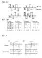
- FIGS. 7 a and 7 billustrate averaging two gray levels, particularly, in a ratio of 1:1 according to an embodiment of the present invention. More particularly, FIG. 7 a shows a pattern of the liquid crystal panel optimal for adopting an 1:1 average driving method of two gray levels and FIG. 7 b shows an application pattern for each frame of the gray level voltage applied to FIG. 7 a.
- gray level voltagesare applied with spatially arrayed 12 ⁇ 4 pixels as one unit as shown in FIG. 7 a and with, preferably, 4 frames for each temporal frame as one unit as shown in FIG. 7 b .
- the pixelscan be pixels of each of R, G and B or can be pixel unit grouping the RGB into one unit.
- a gray level voltage A less than a normal gray level voltage(plotted as a broken line) is applied to a first gate line of a first data line.
- a gray level voltage A higher than the normal gray level voltageis applied to the first gate line of the first data line.
- the gray level voltage less than the normal gray level voltagemay a voltage corresponding to gray level data resulted from the subtraction of a first gray level correction value from the input gray level data n from the external or may a voltage corresponding to the first gray level correction value corresponding to the gray level data.
- the gray level voltage higher than the normal gray level voltagemay a voltage corresponding to gray level data resulted from the addition of a second gray level correction value from the input gray level data n from the external or may a voltage corresponding to the second gray level correction value corresponding to the gray level data.
- the gray levelis represented by averaging two voltages for all sub pixel of the RGB in the above embodiment, the gray level can be represented by differentially applying voltage only for one or two sub-pixels of the RGB.
- FIG. 8illustrates an operation of m and m′ for a particular n on a gamma curve for the liquid crystal display for wide viewing angle as described in FIGS. 7 a and 7 b.
- the gamma curverepresents a relation between each gray level and light transmissivity and m and m′ are assumed to be the first and second gray level correction value, respectively.
- n, m and m′can be represented as the following expression.
- I ⁇ ( n )I ⁇ ( n - m ) + I ⁇ ( n + m ′ ) 2
- n64 for white gray level and I for black gray level.
- m and m′are the first gray level correction value and the second gray level value, respectively, and m+m′ is preferably at least 20.
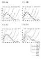
- FIGS. 9 a to 9 dare graphs showing optical properties of the lower gray level inversion based on viewing angles corresponding to the values of m defined according to the present invention.
- FIG. 9 ais a graph showing optical property that the lower gray level inversion is generated at a viewing angle of 36° when m is set to ‘0’
- FIG. 9 bis a graph showing optical property that the lower gray level inversion is generated at a viewing angle of 38° when misset to ‘10’
- FIG. 9 cis a graph showing optical property that the lower gray level inversion is generated at a viewing angle of 56° when m is set to ‘30’
- FIG. 9 dis a graph showing optical property that the lower gray level inversion is generated above a viewing angle of 80° when m is set to ‘50’.
- FIG. 10is a graph for illustrating gray level display according to the present invention.
- the gray level inversionis not generated at gray level values G 1 ′ and G 2 ′ obtained by the averaging operation of the present invention although the gray level is generated in a portion indicated by a circle at gray level values G 1 , G 2 and G 3 corresponding to the gray level of the conventional liquid crystal display.
- gray level to be averaged for each gray levelcan be calculated for same measurement as gamma curve prior to the gray level averaging. Also, it can be confirmed that a brightness average is constant in one pixel in a constant period by satisfying conditions that magnitude of positive and negative polarities should be symmetrical without DC component during a constant period in one pixel.
- the cause of flicker generated by the swing of the common electrode voltagecan be removed. Also, since pixels with different screen brightness due to difference of response time of liquid crystals can be properly averaged so that an observer cannot perceive the brightness difference, the cause of flicker generated by the difference of the response time of the liquid crystals can be removed.
- FIGS. 11 a and 11 billustrate averaging two gray levels, particularly, in a ratio of 2:1, according to another embodiment of the present invention. More particularly, FIG. 11 a shows a pattern of the liquid crystal panel optimal for adopting an 2:1 average driving method of two gray levels and FIG. 11 b shows an application pattern for each frame of the gray level voltage applied to FIG. 11 a.
- gray level voltagesare applied with spatially arrayed 54 ⁇ 3 pixels as one unit as shown in FIG. 11 a and with, preferably, 6 frames for each temporal frame as one unit as shown in FIG. 11 b.
- the pixelscan be pixels of each of R, G and B or can be pixel unit grouping the RGB into one unit.
- FIG. 11 aonly half unit having 27 ⁇ 3 pixels is shown in the figure.
- the gray level voltageis applied to each of frame while pixels are altered in a manner of A 1 ⁇ >A 2 , B 1 ⁇ >B 2 , and C 1 ⁇ >C 2 (i.e in a manner of inversion relation for each frame).
- first frame, fourth frame, etc.when first frame, fourth frame, etc., are driven, a gray level voltage A 1 less than a normal gray level voltage is applied to a first gate line of a first data line.
- second and third frames, fifth and sixth frames, etc.are driven, a gray level voltage higher than the normal gray level voltage is applied to the first gate line of the first data line.
- the gray level voltage less than the normal gray level voltagemay a voltage corresponding to gray level data n ⁇ m resulted from the subtraction of a first gray level correction value m from the input gray level data n from the external or may a voltage corresponding to the first gray level correction value m corresponding to the gray level data.
- FIG. 12is a graph for illustrating operation of m and m′ for a particular n on a gamma curve of FIGS. 11 a and 11 b.
- m′ in which gray level inversion is not generated within a range in which visibility is not seriously affected while adjusting the value of m′may be obtained.
- n, m and m′can be represented as the following expression.
- I ⁇ ( n )2 ⁇ I ⁇ ( n - m ) + I ⁇ ( n + m ′ ) 3
- n64 for white gray level and 1 for black gray level.
- m and m′are the first gray level correction value and the second gray level value, respectively, and m+m′ is preferably at least 20.
Landscapes
- Physics & Mathematics (AREA)
- Engineering & Computer Science (AREA)
- General Physics & Mathematics (AREA)
- Computer Hardware Design (AREA)
- Theoretical Computer Science (AREA)
- Crystallography & Structural Chemistry (AREA)
- Chemical & Material Sciences (AREA)
- Nonlinear Science (AREA)
- Mathematical Physics (AREA)
- Optics & Photonics (AREA)
- Control Of Indicators Other Than Cathode Ray Tubes (AREA)
- Liquid Crystal Display Device Control (AREA)
- Liquid Crystal (AREA)
Abstract
Description
Claims (18)
Applications Claiming Priority (2)
| Application Number | Priority Date | Filing Date | Title |
|---|---|---|---|
| KR1020010053843AKR100806901B1 (en) | 2001-09-03 | 2001-09-03 | LCD for wide viewing angle mode and driving method thereof |
| KR2001-53843 | 2001-09-03 |
Publications (2)
| Publication Number | Publication Date |
|---|---|
| US20030058211A1 US20030058211A1 (en) | 2003-03-27 |
| US7205970B2true US7205970B2 (en) | 2007-04-17 |
Family
ID=36501778
Family Applications (1)
| Application Number | Title | Priority Date | Filing Date |
|---|---|---|---|
| US10/233,869Expired - Fee RelatedUS7205970B2 (en) | 2001-09-03 | 2002-09-03 | Liquid crystal display for wide viewing angle, and driving method thereof |
Country Status (5)
| Country | Link |
|---|---|
| US (1) | US7205970B2 (en) |
| JP (1) | JP4558263B2 (en) |
| KR (1) | KR100806901B1 (en) |
| CN (1) | CN1221934C (en) |
| TW (1) | TWI233586B (en) |
Cited By (13)
| Publication number | Priority date | Publication date | Assignee | Title |
|---|---|---|---|---|
| US20040113879A1 (en)* | 2002-12-10 | 2004-06-17 | Hitachi, Ltd. | Liquid-crystal display device and method of driving liquid-crystal display device |
| US20040239698A1 (en)* | 2003-03-31 | 2004-12-02 | Fujitsu Display Technologies Corporation | Image processing method and liquid-crystal display device using the same |
| US20050201615A1 (en)* | 2004-03-12 | 2005-09-15 | Vastview Technology Inc. | Method for color correction |
| US20060007090A1 (en)* | 2002-09-30 | 2006-01-12 | Magink Display Technologies, Ltd. | Distinct color lcd apparatus |
| US20070252801A1 (en)* | 2006-05-01 | 2007-11-01 | Lg.Philips Lcd Co., Ltd. | Liquid crystal display and driving method thereof |
| US20070263017A1 (en)* | 2005-11-15 | 2007-11-15 | Nec Corporation | Display device, data driver ic, and timing controller |
| US20080042959A1 (en)* | 2004-11-10 | 2008-02-21 | Amir Ben-Shalom | Drive scheme for a cholesteric liquid crystal display device |
| US20080143753A1 (en)* | 2006-12-13 | 2008-06-19 | Wistron Corporation | Method and device of rapidly generating a gray-level versus brightness curve of a display |
| US20130088533A1 (en)* | 2011-10-11 | 2013-04-11 | Chimei Innolux Corporation | Driving method of blue phase liquid crystal display apparatus |
| US10108049B2 (en) | 2010-06-04 | 2018-10-23 | Apple Inc. | Gray scale inversion reduction or prevention in liquid crystal displays |
| US10755655B2 (en) | 2018-01-17 | 2020-08-25 | Novatek Microelectronics Corp. | Source driver and operation method for improving display quality |
| US10791266B1 (en) | 2019-06-23 | 2020-09-29 | Novatek Microelectronics Corp. | Image processing circuit and method |
| US20220189424A1 (en)* | 2020-09-03 | 2022-06-16 | Tcl China Star Optoelectronics Technology Co., Ltd. | Method of controlling display panel, display panel, and display device |
Families Citing this family (36)
| Publication number | Priority date | Publication date | Assignee | Title |
|---|---|---|---|---|
| KR100806901B1 (en)* | 2001-09-03 | 2008-02-22 | 삼성전자주식회사 | LCD for wide viewing angle mode and driving method thereof |
| KR100890026B1 (en)* | 2002-11-20 | 2009-03-25 | 삼성전자주식회사 | Driving device of liquid crystal display and method thereof |
| US7259893B2 (en)* | 2002-12-19 | 2007-08-21 | Electronics For Imaging, Inc. | Methods and apparatus for gray component replacement blending |
| TW584831B (en)* | 2003-02-07 | 2004-04-21 | Au Optronics Corp | Dynamic gamma value adjustment method and circuit of liquid crystal display and drive circuit of liquid crystal display panel |
| KR100697378B1 (en)* | 2003-03-10 | 2007-03-20 | 비오이 하이디스 테크놀로지 주식회사 | LCD and its driving method |
| JP4055679B2 (en)* | 2003-08-25 | 2008-03-05 | セイコーエプソン株式会社 | Electro-optical device, driving method of electro-optical device, and electronic apparatus |
| TWI285870B (en)* | 2003-08-27 | 2007-08-21 | Chi Mei Optoelectronics Corp | Liquid crystal display and driving method |
| US7145558B2 (en)* | 2003-09-03 | 2006-12-05 | Motorola, Inc. | Selective illumination of regions of an electronic display |
| EP1553553A3 (en)* | 2004-01-07 | 2008-07-30 | Chi Mei Optoelectronics Corporation | Liquid crystal display driver for compensating viewing angle |
| CN100454086C (en)* | 2004-01-07 | 2009-01-21 | 奇美电子股份有限公司 | Liquid crystal display and driving method |
| EP1587049A1 (en)* | 2004-04-15 | 2005-10-19 | Barco N.V. | Method and device for improving conformance of a display panel to a display standard in the whole display area and for different viewing angles |
| KR100589324B1 (en)* | 2004-05-11 | 2006-06-14 | 삼성에스디아이 주식회사 | Light emitting display device and driving method thereof |
| JP2005352483A (en)* | 2004-06-09 | 2005-12-22 | Samsung Electronics Co Ltd | Liquid crystal display device and driving method thereof |
| KR101039025B1 (en)* | 2004-06-25 | 2011-06-03 | 삼성전자주식회사 | Display device, drive device for display device and driving method |
| JP2006084860A (en)* | 2004-09-16 | 2006-03-30 | Sharp Corp | Method for driving liquid crystal display device and liquid crystal display device |
| KR101100882B1 (en) | 2004-11-05 | 2012-01-02 | 삼성전자주식회사 | Liquid crystal display and its driving device |
| TWI271695B (en)* | 2005-03-29 | 2007-01-21 | Chi Mei Optoelectronics Corp | Driving system for color display |
| KR101189217B1 (en)* | 2006-02-07 | 2012-10-09 | 삼성디스플레이 주식회사 | Liquid crystlal display |
| JP5043847B2 (en)* | 2006-08-24 | 2012-10-10 | シャープ株式会社 | Liquid crystal display |
| WO2008023602A1 (en)* | 2006-08-24 | 2008-02-28 | Sharp Kabushiki Kaisha | Liquid crystal display |
| TW200820164A (en)* | 2006-10-16 | 2008-05-01 | Au Optronics Corp | Display driving method |
| KR20080054190A (en)* | 2006-12-12 | 2008-06-17 | 삼성전자주식회사 | Display device and driving method thereof |
| JP5049101B2 (en)* | 2006-12-21 | 2012-10-17 | 株式会社ジャパンディスプレイイースト | Liquid crystal display |
| CN101635133B (en)* | 2008-07-21 | 2013-10-16 | 群创光电股份有限公司 | Liquid crystal display device and pixel driving method |
| KR101356370B1 (en) | 2009-07-31 | 2014-01-27 | 엘지디스플레이 주식회사 | Method of Correcting Data And Liquid Crystal Display Using The Same |
| US8791930B2 (en)* | 2009-09-30 | 2014-07-29 | Innolux Corporation | Device and method for improving contrast ratio of display panel and image display system |
| US8976096B2 (en) | 2009-11-27 | 2015-03-10 | Sharp Kabushiki Kaisha | Liquid crystal display device, television receiver, and display method for liquid crystal display device |
| JP5797557B2 (en)* | 2009-11-27 | 2015-10-21 | シャープ株式会社 | Liquid crystal display device, television receiver |
| JP2010204674A (en)* | 2010-04-02 | 2010-09-16 | Sharp Corp | Liquid crystal display device |
| KR20120075168A (en) | 2010-12-28 | 2012-07-06 | 삼성모바일디스플레이주식회사 | Liquid crystal display and method for method for driving thereof |
| TWI452559B (en)* | 2011-11-14 | 2014-09-11 | Au Optronics Corp | Display panel and driving method thereof |
| TWI488168B (en)* | 2013-01-07 | 2015-06-11 | Au Optronics Corp | Display device with adjustable viewing angle and driving method thereof |
| CN104616631B (en)* | 2015-01-27 | 2017-02-22 | 青岛海信电器股份有限公司 | Display method and device for MVA (multi-domain vertical alignment) wide viewing angle LCD (liquid crystal display) screen |
| CN107123402B (en) | 2017-05-26 | 2019-08-23 | 京东方科技集团股份有限公司 | A kind of display device and its control method |
| US11302264B2 (en)* | 2018-11-02 | 2022-04-12 | Apple Inc. | Systems and methods for compensating for IR drop across a display |
| US20220223095A1 (en)* | 2021-01-11 | 2022-07-14 | Tcl China Star Optoelectronics Technology Co., Ltd. | Display panel, and method and device for pixel compensation thereof |
Citations (28)
| Publication number | Priority date | Publication date | Assignee | Title |
|---|---|---|---|---|
| US5298915A (en)* | 1989-04-10 | 1994-03-29 | Cirrus Logic, Inc. | System and method for producing a palette of many colors on a display screen having digitally-commanded pixels |
| US5489918A (en)* | 1991-06-14 | 1996-02-06 | Rockwell International Corporation | Method and apparatus for dynamically and adjustably generating active matrix liquid crystal display gray level voltages |
| US5805117A (en)* | 1994-05-12 | 1998-09-08 | Samsung Electronics Co., Ltd. | Large area tiled modular display system |
| US5852429A (en)* | 1991-04-01 | 1998-12-22 | In Focus Systems, Inc. | Displaying gray shades on display panel implemented with phase-displaced multiple row selections |
| US5894300A (en)* | 1995-09-28 | 1999-04-13 | Nec Corporation | Color image display apparatus and method therefor |
| US6008786A (en)* | 1996-05-22 | 1999-12-28 | International Business Machines Corporation | Method for driving halftone display for a liquid crystal display |
| US6040814A (en)* | 1995-09-19 | 2000-03-21 | Fujitsu Limited | Active-matrix liquid crystal display and method of driving same |
| US6040812A (en)* | 1996-06-19 | 2000-03-21 | Xerox Corporation | Active matrix display with integrated drive circuitry |
| US20020024481A1 (en)* | 2000-07-06 | 2002-02-28 | Kazuyoshi Kawabe | Display device for displaying video data |
| US6407480B1 (en)* | 1998-10-21 | 2002-06-18 | Matsushita Electric Industrial Co., Ltd. | Circuit for driving piezoelectric transformer |
| US6414664B1 (en)* | 1997-11-13 | 2002-07-02 | Honeywell Inc. | Method of and apparatus for controlling contrast of liquid crystal displays while receiving large dynamic range video |
| US6417825B1 (en)* | 1998-09-29 | 2002-07-09 | Sarnoff Corporation | Analog active matrix emissive display |
| US6462835B1 (en)* | 1998-07-15 | 2002-10-08 | Kodak Polychrome Graphics, Llc | Imaging system and method |
| US20020149598A1 (en)* | 2001-01-26 | 2002-10-17 | Greier Paul F. | Method and apparatus for adjusting subpixel intensity values based upon luminance characteristics of the subpixels for improved viewing angle characteristics of liquid crystal displays |
| US6504524B1 (en)* | 2000-03-08 | 2003-01-07 | E Ink Corporation | Addressing methods for displays having zero time-average field |
| US6515641B1 (en)* | 1999-02-25 | 2003-02-04 | Canon Kabushiki Kaisha | Image display apparatus and method of driving image display apparatus |
| US6531997B1 (en)* | 1999-04-30 | 2003-03-11 | E Ink Corporation | Methods for addressing electrophoretic displays |
| US20030058211A1 (en)* | 2001-09-03 | 2003-03-27 | Sang-Il Kim | Liquid crystal display for wide viewing angle, and driving method thereof |
| US20030080926A1 (en)* | 2001-10-30 | 2003-05-01 | Takashi Morimoto | Plasma display device and driving method thereof |
| US20030085906A1 (en)* | 2001-05-09 | 2003-05-08 | Clairvoyante Laboratories, Inc. | Methods and systems for sub-pixel rendering with adaptive filtering |
| US6603450B1 (en)* | 1998-06-05 | 2003-08-05 | Canon Kabushiki Kaisha | Image forming apparatus and image forming method |
| US6611249B1 (en)* | 1998-07-22 | 2003-08-26 | Silicon Graphics, Inc. | System and method for providing a wide aspect ratio flat panel display monitor independent white-balance adjustment and gamma correction capabilities |
| US6683595B2 (en)* | 2000-03-29 | 2004-01-27 | Sony Corporation | Liquid crystal display apparatus and driving method |
| US6714665B1 (en)* | 1994-09-02 | 2004-03-30 | Sarnoff Corporation | Fully automated iris recognition system utilizing wide and narrow fields of view |
| US20040090402A1 (en)* | 2002-11-04 | 2004-05-13 | Ifire Technology Inc. | Method and apparatus for gray-scale gamma correction for electroluminescent displays |
| US6753854B1 (en)* | 1999-04-28 | 2004-06-22 | Semiconductor Energy Laboratory Co., Ltd. | Display device |
| US20050024353A1 (en)* | 2001-11-20 | 2005-02-03 | E Ink Corporation | Methods for driving electro-optic displays |
| US20050093850A1 (en)* | 2002-03-04 | 2005-05-05 | Sanyo Electric Co., Ltd. | Organic electro luminescense display apparatus and application thereof |
Family Cites Families (14)
| Publication number | Priority date | Publication date | Assignee | Title |
|---|---|---|---|---|
| JPH04116893U (en)* | 1991-03-29 | 1992-10-20 | 沖電気工業株式会社 | liquid crystal display device |
| JPH06167951A (en)* | 1992-11-30 | 1994-06-14 | Sharp Corp | Display device drive circuit |
| JPH06250147A (en)* | 1993-02-25 | 1994-09-09 | Sanyo Electric Co Ltd | Liquid crystal display device, device and method for driving the same |
| JP3202450B2 (en)* | 1993-10-20 | 2001-08-27 | 日本電気株式会社 | Liquid crystal display |
| JPH07191634A (en)* | 1993-12-27 | 1995-07-28 | Nec Corp | Active matrix type liquid crystal display device |
| KR0149296B1 (en)* | 1995-08-29 | 1998-12-15 | 김광호 | Wide viewing angle driving circuit and its driving method |
| JPH0990910A (en)* | 1995-09-26 | 1997-04-04 | Matsushita Electric Ind Co Ltd | Driving method of liquid crystal display device and liquid crystal display device |
| JPH11153979A (en)* | 1997-11-19 | 1999-06-08 | Sharp Corp | Liquid crystal display device |
| JP4489208B2 (en)* | 1999-05-31 | 2010-06-23 | オリンパス株式会社 | Image display device |
| KR100601621B1 (en)* | 1999-10-05 | 2006-07-14 | 삼성전자주식회사 | Average brightness of screen in ferroelectric liquid crystal display |
| JP2001117074A (en)* | 1999-10-18 | 2001-04-27 | Hitachi Ltd | Liquid crystal display |
| JP3598913B2 (en)* | 1999-11-22 | 2004-12-08 | 松下電器産業株式会社 | Liquid crystal display |
| KR100670048B1 (en)* | 2000-02-03 | 2007-01-16 | 삼성전자주식회사 | Liquid crystal display device and driving method thereof |
| JP2001075542A (en)* | 2000-07-10 | 2001-03-23 | Semiconductor Energy Lab Co Ltd | Correction system and its operating method |
- 2001
- 2001-09-03KRKR1020010053843Apatent/KR100806901B1/ennot_activeExpired - Fee Related
- 2001-10-25TWTW090126378Apatent/TWI233586B/ennot_activeIP Right Cessation
- 2002
- 2002-06-21JPJP2002181329Apatent/JP4558263B2/ennot_activeExpired - Fee Related
- 2002-09-03CNCNB021437513Apatent/CN1221934C/ennot_activeExpired - Fee Related
- 2002-09-03USUS10/233,869patent/US7205970B2/ennot_activeExpired - Fee Related
Patent Citations (29)
| Publication number | Priority date | Publication date | Assignee | Title |
|---|---|---|---|---|
| US5298915A (en)* | 1989-04-10 | 1994-03-29 | Cirrus Logic, Inc. | System and method for producing a palette of many colors on a display screen having digitally-commanded pixels |
| US5852429A (en)* | 1991-04-01 | 1998-12-22 | In Focus Systems, Inc. | Displaying gray shades on display panel implemented with phase-displaced multiple row selections |
| US5489918A (en)* | 1991-06-14 | 1996-02-06 | Rockwell International Corporation | Method and apparatus for dynamically and adjustably generating active matrix liquid crystal display gray level voltages |
| US5805117A (en)* | 1994-05-12 | 1998-09-08 | Samsung Electronics Co., Ltd. | Large area tiled modular display system |
| US6714665B1 (en)* | 1994-09-02 | 2004-03-30 | Sarnoff Corporation | Fully automated iris recognition system utilizing wide and narrow fields of view |
| US6040814A (en)* | 1995-09-19 | 2000-03-21 | Fujitsu Limited | Active-matrix liquid crystal display and method of driving same |
| US5894300A (en)* | 1995-09-28 | 1999-04-13 | Nec Corporation | Color image display apparatus and method therefor |
| US6008786A (en)* | 1996-05-22 | 1999-12-28 | International Business Machines Corporation | Method for driving halftone display for a liquid crystal display |
| US6040812A (en)* | 1996-06-19 | 2000-03-21 | Xerox Corporation | Active matrix display with integrated drive circuitry |
| US6414664B1 (en)* | 1997-11-13 | 2002-07-02 | Honeywell Inc. | Method of and apparatus for controlling contrast of liquid crystal displays while receiving large dynamic range video |
| US6603450B1 (en)* | 1998-06-05 | 2003-08-05 | Canon Kabushiki Kaisha | Image forming apparatus and image forming method |
| US6462835B1 (en)* | 1998-07-15 | 2002-10-08 | Kodak Polychrome Graphics, Llc | Imaging system and method |
| US6611249B1 (en)* | 1998-07-22 | 2003-08-26 | Silicon Graphics, Inc. | System and method for providing a wide aspect ratio flat panel display monitor independent white-balance adjustment and gamma correction capabilities |
| US6417825B1 (en)* | 1998-09-29 | 2002-07-09 | Sarnoff Corporation | Analog active matrix emissive display |
| US6407480B1 (en)* | 1998-10-21 | 2002-06-18 | Matsushita Electric Industrial Co., Ltd. | Circuit for driving piezoelectric transformer |
| US6515641B1 (en)* | 1999-02-25 | 2003-02-04 | Canon Kabushiki Kaisha | Image display apparatus and method of driving image display apparatus |
| US6753854B1 (en)* | 1999-04-28 | 2004-06-22 | Semiconductor Energy Laboratory Co., Ltd. | Display device |
| US6531997B1 (en)* | 1999-04-30 | 2003-03-11 | E Ink Corporation | Methods for addressing electrophoretic displays |
| US6504524B1 (en)* | 2000-03-08 | 2003-01-07 | E Ink Corporation | Addressing methods for displays having zero time-average field |
| US6683595B2 (en)* | 2000-03-29 | 2004-01-27 | Sony Corporation | Liquid crystal display apparatus and driving method |
| US7057597B2 (en)* | 2000-03-29 | 2006-06-06 | Sony Corporation | Liquid crystal display apparatus and driving method |
| US20020024481A1 (en)* | 2000-07-06 | 2002-02-28 | Kazuyoshi Kawabe | Display device for displaying video data |
| US20020149598A1 (en)* | 2001-01-26 | 2002-10-17 | Greier Paul F. | Method and apparatus for adjusting subpixel intensity values based upon luminance characteristics of the subpixels for improved viewing angle characteristics of liquid crystal displays |
| US20030085906A1 (en)* | 2001-05-09 | 2003-05-08 | Clairvoyante Laboratories, Inc. | Methods and systems for sub-pixel rendering with adaptive filtering |
| US20030058211A1 (en)* | 2001-09-03 | 2003-03-27 | Sang-Il Kim | Liquid crystal display for wide viewing angle, and driving method thereof |
| US20030080926A1 (en)* | 2001-10-30 | 2003-05-01 | Takashi Morimoto | Plasma display device and driving method thereof |
| US20050024353A1 (en)* | 2001-11-20 | 2005-02-03 | E Ink Corporation | Methods for driving electro-optic displays |
| US20050093850A1 (en)* | 2002-03-04 | 2005-05-05 | Sanyo Electric Co., Ltd. | Organic electro luminescense display apparatus and application thereof |
| US20040090402A1 (en)* | 2002-11-04 | 2004-05-13 | Ifire Technology Inc. | Method and apparatus for gray-scale gamma correction for electroluminescent displays |
Cited By (23)
| Publication number | Priority date | Publication date | Assignee | Title |
|---|---|---|---|---|
| US7719501B2 (en)* | 2002-09-30 | 2010-05-18 | Magink Display Technologies Ltd. | Distinct color LCD apparatus |
| US20060007090A1 (en)* | 2002-09-30 | 2006-01-12 | Magink Display Technologies, Ltd. | Distinct color lcd apparatus |
| US7477223B2 (en)* | 2002-12-10 | 2009-01-13 | Hitachi, Ltd. | Liquid-crystal display device and method of driving liquid-crystal display device |
| US20040113879A1 (en)* | 2002-12-10 | 2004-06-17 | Hitachi, Ltd. | Liquid-crystal display device and method of driving liquid-crystal display device |
| US8094143B2 (en)* | 2003-03-31 | 2012-01-10 | Sharp Kabushiki Kaisha | Image processing method and liquid-crystal display device using the same |
| US8502762B2 (en)* | 2003-03-31 | 2013-08-06 | Sharp Kabushiki Kaisha | Image processing method and liquid-crystal display device using the same |
| US20040239698A1 (en)* | 2003-03-31 | 2004-12-02 | Fujitsu Display Technologies Corporation | Image processing method and liquid-crystal display device using the same |
| US20100103206A1 (en)* | 2003-03-31 | 2010-04-29 | Sharp Kabushiki Kaisha | Image processing method and liquid-crystal display device using the same |
| US7375854B2 (en)* | 2004-03-12 | 2008-05-20 | Vastview Technology, Inc. | Method for color correction |
| US20050201615A1 (en)* | 2004-03-12 | 2005-09-15 | Vastview Technology Inc. | Method for color correction |
| US8013819B2 (en) | 2004-11-10 | 2011-09-06 | Magink Display Technologies Ltd | Drive scheme for a cholesteric liquid crystal display device |
| US20080042959A1 (en)* | 2004-11-10 | 2008-02-21 | Amir Ben-Shalom | Drive scheme for a cholesteric liquid crystal display device |
| US7898517B2 (en) | 2005-11-15 | 2011-03-01 | Renesas Electronics Corporation | Display device, data driver IC, and timing controller |
| US20070263017A1 (en)* | 2005-11-15 | 2007-11-15 | Nec Corporation | Display device, data driver ic, and timing controller |
| US7880703B2 (en)* | 2006-05-01 | 2011-02-01 | Lg Display Co., Ltd. | Liquid crystal display and driving method thereof |
| US20070252801A1 (en)* | 2006-05-01 | 2007-11-01 | Lg.Philips Lcd Co., Ltd. | Liquid crystal display and driving method thereof |
| US20080143753A1 (en)* | 2006-12-13 | 2008-06-19 | Wistron Corporation | Method and device of rapidly generating a gray-level versus brightness curve of a display |
| US10108049B2 (en) | 2010-06-04 | 2018-10-23 | Apple Inc. | Gray scale inversion reduction or prevention in liquid crystal displays |
| US20130088533A1 (en)* | 2011-10-11 | 2013-04-11 | Chimei Innolux Corporation | Driving method of blue phase liquid crystal display apparatus |
| US10755655B2 (en) | 2018-01-17 | 2020-08-25 | Novatek Microelectronics Corp. | Source driver and operation method for improving display quality |
| US10791266B1 (en) | 2019-06-23 | 2020-09-29 | Novatek Microelectronics Corp. | Image processing circuit and method |
| US20220189424A1 (en)* | 2020-09-03 | 2022-06-16 | Tcl China Star Optoelectronics Technology Co., Ltd. | Method of controlling display panel, display panel, and display device |
| US11600239B2 (en)* | 2020-09-03 | 2023-03-07 | Tcl China Star Optoelectronics Technology Co., Ltd. | Method of controlling display panel, display panel, and display device |
Also Published As
| Publication number | Publication date |
|---|---|
| US20030058211A1 (en) | 2003-03-27 |
| JP2003099017A (en) | 2003-04-04 |
| CN1404029A (en) | 2003-03-19 |
| KR100806901B1 (en) | 2008-02-22 |
| KR20030020153A (en) | 2003-03-08 |
| JP4558263B2 (en) | 2010-10-06 |
| CN1221934C (en) | 2005-10-05 |
| TWI233586B (en) | 2005-06-01 |
Similar Documents
| Publication | Publication Date | Title |
|---|---|---|
| US7205970B2 (en) | Liquid crystal display for wide viewing angle, and driving method thereof | |
| KR101374425B1 (en) | Liquid crystal display and method of controlling dot inversion thereof | |
| JP5399432B2 (en) | Liquid crystal display device and driving method thereof | |
| KR101329438B1 (en) | Liquid crystal display | |
| US7898536B2 (en) | Display apparatus and method of driving the same | |
| US20100231617A1 (en) | Data processing device, liquid crystal display devce, television receiver, and data processing method | |
| US20070001963A1 (en) | Liquid crystal display unit and driving method therefor and drive device for liquid crystal display panel | |
| US20080218463A1 (en) | Display device and method for driving the same | |
| US8963908B2 (en) | Liquid crystal display device having a data driving circuit with overdrive control using polarity control | |
| JP2011053693A (en) | Liquid crystal display device reduced in flicker, and method for reducing flicker | |
| CN103268759B (en) | Data processing equipment, liquid crystal indicator, television receiver and data processing method | |
| CN101154005A (en) | Electro-optical devices and electronic devices | |
| US8982287B2 (en) | Data processing apparatus, liquid crystal display device, television receiver, and data processing method | |
| US7928943B2 (en) | Liquid crystal display | |
| US20100164940A1 (en) | Liquid crystal display and driving method thereof | |
| US8570316B2 (en) | Liquid crystal display | |
| US20080084412A1 (en) | Liquid crystal display device and method for driving the same | |
| US7746330B2 (en) | Circuit and method for improving image quality of a liquid crystal display | |
| KR101651290B1 (en) | Liquid crystal display and method of controlling a polarity of data thereof | |
| KR20110130707A (en) | LCD and its dot inversion control method | |
| KR20110030885A (en) | LCD and its driving method | |
| KR20110032488A (en) | LCD Display |
Legal Events
| Date | Code | Title | Description |
|---|---|---|---|
| AS | Assignment | Owner name:SAMSUNG ELECTRONICS CO., LTD., KOREA, REPUBLIC OF Free format text:ASSIGNMENT OF ASSIGNORS INTEREST;ASSIGNORS:KIM, SANG-IL;PARK, CHEOL-WOO;YANG, YOUNG-CHUL;REEL/FRAME:013534/0623 Effective date:20021021 | |
| AS | Assignment | Owner name:SAMSUNG ELECTRONICS CO., LTD., KOREA, REPUBLIC OF Free format text:CORRECTIVE RECORDATION FORM COVER SHEET TO CORRECT ASSIGNOR'S NAME FROM YOUNG-CHUL YANG TO YOUNG-CHOL YANG; RECORDED AT REEL 013534 FRAME 0623.;ASSIGNORS:KIM, SANG-IL;PARK, CHEOL-WOO;YANG, YOUNG-CHOL;REEL/FRAME:014197/0990 Effective date:20021021 | |
| STCF | Information on status: patent grant | Free format text:PATENTED CASE | |
| FEPP | Fee payment procedure | Free format text:PAYOR NUMBER ASSIGNED (ORIGINAL EVENT CODE: ASPN); ENTITY STATUS OF PATENT OWNER: LARGE ENTITY | |
| FPAY | Fee payment | Year of fee payment:4 | |
| AS | Assignment | Owner name:SAMSUNG DISPLAY CO., LTD., KOREA, REPUBLIC OF Free format text:ASSIGNMENT OF ASSIGNORS INTEREST;ASSIGNOR:SAMSUNG ELECTRONICS CO., LTD.;REEL/FRAME:028984/0774 Effective date:20120904 | |
| FPAY | Fee payment | Year of fee payment:8 | |
| FEPP | Fee payment procedure | Free format text:PAYER NUMBER DE-ASSIGNED (ORIGINAL EVENT CODE: RMPN); ENTITY STATUS OF PATENT OWNER: LARGE ENTITY Free format text:PAYOR NUMBER ASSIGNED (ORIGINAL EVENT CODE: ASPN); ENTITY STATUS OF PATENT OWNER: LARGE ENTITY | |
| FEPP | Fee payment procedure | Free format text:MAINTENANCE FEE REMINDER MAILED (ORIGINAL EVENT CODE: REM.); ENTITY STATUS OF PATENT OWNER: LARGE ENTITY | |
| LAPS | Lapse for failure to pay maintenance fees | Free format text:PATENT EXPIRED FOR FAILURE TO PAY MAINTENANCE FEES (ORIGINAL EVENT CODE: EXP.); ENTITY STATUS OF PATENT OWNER: LARGE ENTITY | |
| STCH | Information on status: patent discontinuation | Free format text:PATENT EXPIRED DUE TO NONPAYMENT OF MAINTENANCE FEES UNDER 37 CFR 1.362 | |
| FP | Lapsed due to failure to pay maintenance fee | Effective date:20190417 |