US7205228B2 - Selective metal encapsulation schemes - Google Patents
Selective metal encapsulation schemesDownload PDFInfo
- Publication number
- US7205228B2 US7205228B2US10/812,480US81248004AUS7205228B2US 7205228 B2US7205228 B2US 7205228B2US 81248004 AUS81248004 AUS 81248004AUS 7205228 B2US7205228 B2US 7205228B2
- Authority
- US
- United States
- Prior art keywords
- layer
- depositing
- steps
- protective layer
- substrate surface
- Prior art date
- Legal status (The legal status is an assumption and is not a legal conclusion. Google has not performed a legal analysis and makes no representation as to the accuracy of the status listed.)
- Expired - Fee Related
Links
- 229910052751metalInorganic materials0.000titledescription61
- 239000002184metalSubstances0.000titledescription61
- 238000005538encapsulationMethods0.000titledescription7
- 239000010410layerSubstances0.000claimsabstractdescription238
- 239000000758substrateSubstances0.000claimsabstractdescription144
- 238000000151depositionMethods0.000claimsabstractdescription137
- 238000000034methodMethods0.000claimsabstractdescription116
- 239000011241protective layerSubstances0.000claimsabstractdescription85
- 230000008021depositionEffects0.000claimsabstractdescription76
- 238000012545processingMethods0.000claimsabstractdescription38
- 239000003989dielectric materialSubstances0.000claimsabstractdescription34
- 239000004065semiconductorSubstances0.000claimsabstractdescription14
- 239000000463materialSubstances0.000claimsdescription81
- 229920002120photoresistant polymerPolymers0.000claimsdescription46
- 238000005530etchingMethods0.000claimsdescription38
- 230000000977initiatory effectEffects0.000claimsdescription34
- KDLHZDBZIXYQEI-UHFFFAOYSA-NPalladiumChemical compound[Pd]KDLHZDBZIXYQEI-UHFFFAOYSA-N0.000claimsdescription32
- RYGMFSIKBFXOCR-UHFFFAOYSA-NCopperChemical compound[Cu]RYGMFSIKBFXOCR-UHFFFAOYSA-N0.000claimsdescription31
- 239000010949copperSubstances0.000claimsdescription30
- 229910052802copperInorganic materials0.000claimsdescription30
- 229910003481amorphous carbonInorganic materials0.000claimsdescription21
- 239000010941cobaltSubstances0.000claimsdescription21
- GUTLYIVDDKVIGB-UHFFFAOYSA-Ncobalt atomChemical compound[Co]GUTLYIVDDKVIGB-UHFFFAOYSA-N0.000claimsdescription21
- 229910017052cobaltInorganic materials0.000claimsdescription20
- 229910052763palladiumInorganic materials0.000claimsdescription16
- 239000004020conductorSubstances0.000claimsdescription14
- BASFCYQUMIYNBI-UHFFFAOYSA-NplatinumChemical compound[Pt]BASFCYQUMIYNBI-UHFFFAOYSA-N0.000claimsdescription14
- 230000004913activationEffects0.000claimsdescription13
- 238000004380ashingMethods0.000claimsdescription10
- 238000004140cleaningMethods0.000claimsdescription10
- XEEYBQQBJWHFJM-UHFFFAOYSA-NIronChemical compound[Fe]XEEYBQQBJWHFJM-UHFFFAOYSA-N0.000claimsdescription8
- PXHVJJICTQNCMI-UHFFFAOYSA-NNickelChemical compound[Ni]PXHVJJICTQNCMI-UHFFFAOYSA-N0.000claimsdescription8
- 238000005229chemical vapour depositionMethods0.000claimsdescription8
- WFKWXMTUELFFGS-UHFFFAOYSA-NtungstenChemical compound[W]WFKWXMTUELFFGS-UHFFFAOYSA-N0.000claimsdescription8
- 229910052721tungstenInorganic materials0.000claimsdescription8
- 239000010937tungstenSubstances0.000claimsdescription8
- 229910052697platinumInorganic materials0.000claimsdescription7
- 239000000126substanceSubstances0.000claimsdescription6
- ATJFFYVFTNAWJD-UHFFFAOYSA-NTinChemical compound[Sn]ATJFFYVFTNAWJD-UHFFFAOYSA-N0.000claimsdescription5
- 229910045601alloyInorganic materials0.000claimsdescription5
- 239000000956alloySubstances0.000claimsdescription5
- 229910052715tantalumInorganic materials0.000claimsdescription5
- GUVRBAGPIYLISA-UHFFFAOYSA-Ntantalum atomChemical compound[Ta]GUVRBAGPIYLISA-UHFFFAOYSA-N0.000claimsdescription5
- 229910052718tinInorganic materials0.000claimsdescription5
- ZOKXTWBITQBERF-UHFFFAOYSA-NMolybdenumChemical compound[Mo]ZOKXTWBITQBERF-UHFFFAOYSA-N0.000claimsdescription4
- KJTLSVCANCCWHF-UHFFFAOYSA-NRutheniumChemical group[Ru]KJTLSVCANCCWHF-UHFFFAOYSA-N0.000claimsdescription4
- RTAQQCXQSZGOHL-UHFFFAOYSA-NTitaniumChemical compound[Ti]RTAQQCXQSZGOHL-UHFFFAOYSA-N0.000claimsdescription4
- 229910052742ironInorganic materials0.000claimsdescription4
- 229910052750molybdenumInorganic materials0.000claimsdescription4
- 239000011733molybdenumSubstances0.000claimsdescription4
- 229910052759nickelInorganic materials0.000claimsdescription4
- 229910052758niobiumInorganic materials0.000claimsdescription4
- 239000010955niobiumSubstances0.000claimsdescription4
- GUCVJGMIXFAOAE-UHFFFAOYSA-Nniobium atomChemical compound[Nb]GUCVJGMIXFAOAE-UHFFFAOYSA-N0.000claimsdescription4
- 229910052707rutheniumInorganic materials0.000claimsdescription4
- 239000011135tinSubstances0.000claimsdescription4
- 239000010936titaniumSubstances0.000claimsdescription4
- 229910052719titaniumInorganic materials0.000claimsdescription4
- 239000011368organic materialSubstances0.000claimsdescription3
- 238000005240physical vapour depositionMethods0.000claimsdescription3
- 230000000873masking effectEffects0.000abstractdescription5
- 230000008569processEffects0.000description38
- UORVGPXVDQYIDP-UHFFFAOYSA-NboraneChemical compoundBUORVGPXVDQYIDP-UHFFFAOYSA-N0.000description36
- 239000000243solutionSubstances0.000description31
- 239000000203mixtureSubstances0.000description29
- 238000002161passivationMethods0.000description20
- 229910000085boraneInorganic materials0.000description19
- 239000003638chemical reducing agentSubstances0.000description17
- 239000001257hydrogenSubstances0.000description17
- 229910052739hydrogenInorganic materials0.000description17
- 229910000510noble metalInorganic materials0.000description15
- UFHFLCQGNIYNRP-UHFFFAOYSA-NHydrogenChemical compound[H][H]UFHFLCQGNIYNRP-UHFFFAOYSA-N0.000description12
- 239000000356contaminantSubstances0.000description12
- KRHYYFGTRYWZRS-UHFFFAOYSA-Nhydrofluoric acidSubstancesFKRHYYFGTRYWZRS-UHFFFAOYSA-N0.000description12
- 238000005137deposition processMethods0.000description11
- IJGRMHOSHXDMSA-UHFFFAOYSA-NAtomic nitrogenChemical compoundN#NIJGRMHOSHXDMSA-UHFFFAOYSA-N0.000description10
- 229910000531Co alloyInorganic materials0.000description10
- 150000002739metalsChemical class0.000description10
- QPJSUIGXIBEQAC-UHFFFAOYSA-Nn-(2,4-dichloro-5-propan-2-yloxyphenyl)acetamideChemical compoundCC(C)OC1=CC(NC(C)=O)=C(Cl)C=C1ClQPJSUIGXIBEQAC-UHFFFAOYSA-N0.000description10
- XLYOFNOQVPJJNP-UHFFFAOYSA-NwaterSubstancesOXLYOFNOQVPJJNP-UHFFFAOYSA-N0.000description10
- HEMHJVSKTPXQMS-UHFFFAOYSA-MSodium hydroxideChemical compound[OH-].[Na+]HEMHJVSKTPXQMS-UHFFFAOYSA-M0.000description9
- 230000004888barrier functionEffects0.000description9
- 238000006073displacement reactionMethods0.000description9
- 229910044991metal oxideInorganic materials0.000description9
- 150000004706metal oxidesChemical class0.000description9
- QGZKDVFQNNGYKY-UHFFFAOYSA-NAmmoniaChemical compoundNQGZKDVFQNNGYKY-UHFFFAOYSA-N0.000description8
- 239000007789gasSubstances0.000description8
- 150000003839saltsChemical class0.000description8
- KWYUFKZDYYNOTN-UHFFFAOYSA-MPotassium hydroxideChemical compound[OH-].[K+]KWYUFKZDYYNOTN-UHFFFAOYSA-M0.000description7
- 238000004544sputter depositionMethods0.000description7
- 238000004381surface treatmentMethods0.000description7
- VEXZGXHMUGYJMC-UHFFFAOYSA-NHydrochloric acidChemical compoundClVEXZGXHMUGYJMC-UHFFFAOYSA-N0.000description6
- VYPSYNLAJGMNEJ-UHFFFAOYSA-NSilicium dioxideChemical compoundO=[Si]=OVYPSYNLAJGMNEJ-UHFFFAOYSA-N0.000description6
- RJTANRZEWTUVMA-UHFFFAOYSA-Nboron;n-methylmethanamineChemical compound[B].CNCRJTANRZEWTUVMA-UHFFFAOYSA-N0.000description6
- 230000003197catalytic effectEffects0.000description6
- -1e.g.Inorganic materials0.000description6
- 230000006911nucleationEffects0.000description6
- 238000010899nucleationMethods0.000description6
- 238000001020plasma etchingMethods0.000description6
- 238000000623plasma-assisted chemical vapour depositionMethods0.000description6
- 235000012431wafersNutrition0.000description6
- QTBSBXVTEAMEQO-UHFFFAOYSA-NAcetic acidChemical compoundCC(O)=OQTBSBXVTEAMEQO-UHFFFAOYSA-N0.000description5
- 239000012153distilled waterSubstances0.000description5
- 238000005516engineering processMethods0.000description5
- 150000002431hydrogenChemical class0.000description5
- 238000004519manufacturing processMethods0.000description5
- 229910052757nitrogenInorganic materials0.000description5
- 238000001039wet etchingMethods0.000description5
- 239000003929acidic solutionSubstances0.000description4
- 229910021529ammoniaInorganic materials0.000description4
- 238000011161developmentMethods0.000description4
- 238000011065in-situ storageMethods0.000description4
- 230000010354integrationEffects0.000description4
- 150000002500ionsChemical class0.000description4
- 150000007522mineralic acidsChemical class0.000description4
- 238000005498polishingMethods0.000description4
- 229910052814silicon oxideInorganic materials0.000description4
- ZOXJGFHDIHLPTG-UHFFFAOYSA-NBoronChemical compound[B]ZOXJGFHDIHLPTG-UHFFFAOYSA-N0.000description3
- 241000393496ElectraSpecies0.000description3
- XUIMIQQOPSSXEZ-UHFFFAOYSA-NSiliconChemical compound[Si]XUIMIQQOPSSXEZ-UHFFFAOYSA-N0.000description3
- QAOWNCQODCNURD-UHFFFAOYSA-NSulfuric acidChemical compoundOS(O)(=O)=OQAOWNCQODCNURD-UHFFFAOYSA-N0.000description3
- CPJYFACXEHYLFS-UHFFFAOYSA-N[B].[W].[Co]Chemical compound[B].[W].[Co]CPJYFACXEHYLFS-UHFFFAOYSA-N0.000description3
- 229910052782aluminiumInorganic materials0.000description3
- XAGFODPZIPBFFR-UHFFFAOYSA-NaluminiumChemical compound[Al]XAGFODPZIPBFFR-UHFFFAOYSA-N0.000description3
- 229910052796boronInorganic materials0.000description3
- JPNWDVUTVSTKMV-UHFFFAOYSA-Ncobalt tungstenChemical compound[Co].[W]JPNWDVUTVSTKMV-UHFFFAOYSA-N0.000description3
- 150000001875compoundsChemical class0.000description3
- 238000011109contaminationMethods0.000description3
- 238000007796conventional methodMethods0.000description3
- 238000009792diffusion processMethods0.000description3
- 230000000694effectsEffects0.000description3
- 238000001465metallisationMethods0.000description3
- 239000003002pH adjusting agentSubstances0.000description3
- 229920000642polymerPolymers0.000description3
- 230000001681protective effectEffects0.000description3
- 229910052710siliconInorganic materials0.000description3
- 239000010703siliconSubstances0.000description3
- XMVONEAAOPAGAO-UHFFFAOYSA-Nsodium tungstateChemical compound[Na+].[Na+].[O-][W]([O-])(=O)=OXMVONEAAOPAGAO-UHFFFAOYSA-N0.000description3
- KWSLGOVYXMQPPX-UHFFFAOYSA-N5-[3-(trifluoromethyl)phenyl]-2h-tetrazoleChemical compoundFC(F)(F)C1=CC=CC(C2=NNN=N2)=C1KWSLGOVYXMQPPX-UHFFFAOYSA-N0.000description2
- NLXLAEXVIDQMFP-UHFFFAOYSA-NAmmonia chlorideChemical compound[NH4+].[Cl-]NLXLAEXVIDQMFP-UHFFFAOYSA-N0.000description2
- VHUUQVKOLVNVRT-UHFFFAOYSA-NAmmonium hydroxideChemical compound[NH4+].[OH-]VHUUQVKOLVNVRT-UHFFFAOYSA-N0.000description2
- XKRFYHLGVUSROY-UHFFFAOYSA-NArgonChemical compound[Ar]XKRFYHLGVUSROY-UHFFFAOYSA-N0.000description2
- 229910000521B alloyInorganic materials0.000description2
- OKTJSMMVPCPJKN-UHFFFAOYSA-NCarbonChemical compound[C]OKTJSMMVPCPJKN-UHFFFAOYSA-N0.000description2
- QPLDLSVMHZLSFG-UHFFFAOYSA-NCopper oxideChemical compound[Cu]=OQPLDLSVMHZLSFG-UHFFFAOYSA-N0.000description2
- XPDWGBQVDMORPB-UHFFFAOYSA-NFluoroformChemical compoundFC(F)FXPDWGBQVDMORPB-UHFFFAOYSA-N0.000description2
- OAKJQQAXSVQMHS-UHFFFAOYSA-NHydrazineChemical compoundNNOAKJQQAXSVQMHS-UHFFFAOYSA-N0.000description2
- OAICVXFJPJFONN-UHFFFAOYSA-NPhosphorusChemical compound[P]OAICVXFJPJFONN-UHFFFAOYSA-N0.000description2
- 239000004642PolyimideSubstances0.000description2
- FEBFYWHXKVOHDI-UHFFFAOYSA-N[Co].[P][W]Chemical compound[Co].[P][W]FEBFYWHXKVOHDI-UHFFFAOYSA-N0.000description2
- 239000000654additiveSubstances0.000description2
- 239000012298atmosphereSubstances0.000description2
- 125000004429atomChemical group0.000description2
- 230000015572biosynthetic processEffects0.000description2
- WVMHLYQJPRXKLC-UHFFFAOYSA-Nborane;n,n-dimethylmethanamineChemical compoundB.CN(C)CWVMHLYQJPRXKLC-UHFFFAOYSA-N0.000description2
- HZEIHKAVLOJHDG-UHFFFAOYSA-NboranylidynecobaltChemical compound[Co]#BHZEIHKAVLOJHDG-UHFFFAOYSA-N0.000description2
- 229910052799carbonInorganic materials0.000description2
- 229940044175cobalt sulfateDrugs0.000description2
- 229910000361cobalt sulfateInorganic materials0.000description2
- WDHWFGNRFMPTQS-UHFFFAOYSA-Ncobalt tinChemical compound[Co].[Sn]WDHWFGNRFMPTQS-UHFFFAOYSA-N0.000description2
- KTVIXTQDYHMGHF-UHFFFAOYSA-Lcobalt(2+) sulfateChemical compound[Co+2].[O-]S([O-])(=O)=OKTVIXTQDYHMGHF-UHFFFAOYSA-L0.000description2
- 239000011521glassSubstances0.000description2
- 239000011261inert gasSubstances0.000description2
- 239000011229interlayerSubstances0.000description2
- PIBWKRNGBLPSSY-UHFFFAOYSA-Lpalladium(II) chlorideChemical compoundCl[Pd]ClPIBWKRNGBLPSSY-UHFFFAOYSA-L0.000description2
- ACVYVLVWPXVTIT-UHFFFAOYSA-MphosphinateChemical compound[O-][PH2]=OACVYVLVWPXVTIT-UHFFFAOYSA-M0.000description2
- 229910052698phosphorusInorganic materials0.000description2
- 239000011574phosphorusSubstances0.000description2
- 238000005289physical depositionMethods0.000description2
- 229920000090poly(aryl ether)Polymers0.000description2
- 229920001721polyimidePolymers0.000description2
- 238000006722reduction reactionMethods0.000description2
- 229910052702rheniumInorganic materials0.000description2
- WUAPFZMCVAUBPE-UHFFFAOYSA-Nrhenium atomChemical compound[Re]WUAPFZMCVAUBPE-UHFFFAOYSA-N0.000description2
- 239000012279sodium borohydrideSubstances0.000description2
- 229910000033sodium borohydrideInorganic materials0.000description2
- 239000001509sodium citrateSubstances0.000description2
- NLJMYIDDQXHKNR-UHFFFAOYSA-Ksodium citrateChemical compoundO.O.[Na+].[Na+].[Na+].[O-]C(=O)CC(O)(CC([O-])=O)C([O-])=ONLJMYIDDQXHKNR-UHFFFAOYSA-K0.000description2
- 229910001379sodium hypophosphiteInorganic materials0.000description2
- 239000006104solid solutionSubstances0.000description2
- 239000002904solventSubstances0.000description2
- WGTYBPLFGIVFAS-UHFFFAOYSA-Mtetramethylammonium hydroxideChemical compound[OH-].C[N+](C)(C)CWGTYBPLFGIVFAS-UHFFFAOYSA-M0.000description2
- 238000002525ultrasonicationMethods0.000description2
- JBRZTFJDHDCESZ-UHFFFAOYSA-NAsGaChemical compound[As]#[Ga]JBRZTFJDHDCESZ-UHFFFAOYSA-N0.000description1
- 239000005751Copper oxideSubstances0.000description1
- 229910000640Fe alloyInorganic materials0.000description1
- 229910001218Gallium arsenideInorganic materials0.000description1
- 229910000990Ni alloyInorganic materials0.000description1
- 229910001096P alloyInorganic materials0.000description1
- BQCADISMDOOEFD-UHFFFAOYSA-NSilverChemical compound[Ag]BQCADISMDOOEFD-UHFFFAOYSA-N0.000description1
- 229910001128Sn alloyInorganic materials0.000description1
- QAOWNCQODCNURD-UHFFFAOYSA-LSulfateChemical compound[O-]S([O-])(=O)=OQAOWNCQODCNURD-UHFFFAOYSA-L0.000description1
- BOTDANWDWHJENH-UHFFFAOYSA-NTetraethyl orthosilicateChemical compoundCCO[Si](OCC)(OCC)OCCBOTDANWDWHJENH-UHFFFAOYSA-N0.000description1
- 229910021627Tin(IV) chlorideInorganic materials0.000description1
- NRTOMJZYCJJWKI-UHFFFAOYSA-NTitanium nitrideChemical compound[Ti]#NNRTOMJZYCJJWKI-UHFFFAOYSA-N0.000description1
- 229910001080W alloyInorganic materials0.000description1
- ZMMUSLWEDSQDJY-UHFFFAOYSA-N[B].[Sn].[Co]Chemical compound[B].[Sn].[Co]ZMMUSLWEDSQDJY-UHFFFAOYSA-N0.000description1
- QXZUUHYBWMWJHK-UHFFFAOYSA-N[Co].[Ni]Chemical compound[Co].[Ni]QXZUUHYBWMWJHK-UHFFFAOYSA-N0.000description1
- 239000002253acidSubstances0.000description1
- 230000002378acidificating effectEffects0.000description1
- 229910052783alkali metalInorganic materials0.000description1
- 150000001340alkali metalsChemical class0.000description1
- 235000019270ammonium chlorideNutrition0.000description1
- 239000000908ammonium hydroxideSubstances0.000description1
- 238000000137annealingMethods0.000description1
- 230000003466anti-cipated effectEffects0.000description1
- 229910052786argonInorganic materials0.000description1
- 238000000231atomic layer depositionMethods0.000description1
- UMIVXZPTRXBADB-UHFFFAOYSA-NbenzocyclobuteneChemical classC1=CC=C2CCC2=C1UMIVXZPTRXBADB-UHFFFAOYSA-N0.000description1
- 150000001735carboxylic acidsChemical class0.000description1
- 239000003054catalystSubstances0.000description1
- 238000003486chemical etchingMethods0.000description1
- 239000003795chemical substances by applicationSubstances0.000description1
- 150000001805chlorine compoundsChemical class0.000description1
- 239000011248coating agentSubstances0.000description1
- 238000000576coating methodMethods0.000description1
- GVPFVAHMJGGAJG-UHFFFAOYSA-Lcobalt dichlorideChemical group[Cl-].[Cl-].[Co+2]GVPFVAHMJGGAJG-UHFFFAOYSA-L0.000description1
- 229910052681coesiteInorganic materials0.000description1
- 239000008139complexing agentSubstances0.000description1
- 239000002131composite materialSubstances0.000description1
- 229910000431copper oxideInorganic materials0.000description1
- 229910052906cristobaliteInorganic materials0.000description1
- 239000008367deionised waterSubstances0.000description1
- 229910021641deionized waterInorganic materials0.000description1
- 230000002939deleterious effectEffects0.000description1
- 238000013461designMethods0.000description1
- 230000009977dual effectEffects0.000description1
- 230000005684electric fieldEffects0.000description1
- 238000007772electroless platingMethods0.000description1
- 229910052732germaniumInorganic materials0.000description1
- GNPVGFCGXDBREM-UHFFFAOYSA-Ngermanium atomChemical compound[Ge]GNPVGFCGXDBREM-UHFFFAOYSA-N0.000description1
- PCHJSUWPFVWCPO-UHFFFAOYSA-NgoldChemical compound[Au]PCHJSUWPFVWCPO-UHFFFAOYSA-N0.000description1
- 229910052737goldInorganic materials0.000description1
- 239000010931goldSubstances0.000description1
- 239000001307heliumSubstances0.000description1
- 229910052734heliumInorganic materials0.000description1
- SWQJXJOGLNCZEY-UHFFFAOYSA-Nhelium atomChemical compound[He]SWQJXJOGLNCZEY-UHFFFAOYSA-N0.000description1
- 238000007654immersionMethods0.000description1
- 229910052741iridiumInorganic materials0.000description1
- GKOZUEZYRPOHIO-UHFFFAOYSA-Niridium atomChemical compound[Ir]GKOZUEZYRPOHIO-UHFFFAOYSA-N0.000description1
- UGKDIUIOSMUOAW-UHFFFAOYSA-Niron nickelChemical compound[Fe].[Ni]UGKDIUIOSMUOAW-UHFFFAOYSA-N0.000description1
- 238000002955isolationMethods0.000description1
- 230000007246mechanismEffects0.000description1
- 229910021645metal ionInorganic materials0.000description1
- WSFSSNUMVMOOMR-NJFSPNSNSA-NmethanoneChemical compoundO=[14CH2]WSFSSNUMVMOOMR-NJFSPNSNSA-N0.000description1
- 150000004767nitridesChemical class0.000description1
- 229910052756noble gasInorganic materials0.000description1
- 150000002835noble gasesChemical class0.000description1
- 239000012811non-conductive materialSubstances0.000description1
- 229910052762osmiumInorganic materials0.000description1
- SYQBFIAQOQZEGI-UHFFFAOYSA-Nosmium atomChemical compound[Os]SYQBFIAQOQZEGI-UHFFFAOYSA-N0.000description1
- RFLFDJSIZCCYIP-UHFFFAOYSA-Lpalladium(2+);sulfateChemical compound[Pd+2].[O-]S([O-])(=O)=ORFLFDJSIZCCYIP-UHFFFAOYSA-L0.000description1
- 239000002245particleSubstances0.000description1
- SIBIBHIFKSKVRR-UHFFFAOYSA-NphosphanylidynecobaltChemical compound[Co]#PSIBIBHIFKSKVRR-UHFFFAOYSA-N0.000description1
- 238000000206photolithographyMethods0.000description1
- 238000009832plasma treatmentMethods0.000description1
- 238000007747platingMethods0.000description1
- 238000002360preparation methodMethods0.000description1
- 239000011253protective coatingSubstances0.000description1
- 230000009467reductionEffects0.000description1
- 229910052703rhodiumInorganic materials0.000description1
- 239000010948rhodiumSubstances0.000description1
- MHOVAHRLVXNVSD-UHFFFAOYSA-Nrhodium atomChemical compound[Rh]MHOVAHRLVXNVSD-UHFFFAOYSA-N0.000description1
- 239000010980sapphireSubstances0.000description1
- 229910052594sapphireInorganic materials0.000description1
- 239000000377silicon dioxideSubstances0.000description1
- 229910052709silverInorganic materials0.000description1
- 239000004332silverSubstances0.000description1
- 238000005507sprayingMethods0.000description1
- 125000005402stannate groupChemical group0.000description1
- 229910052682stishoviteInorganic materials0.000description1
- IIACRCGMVDHOTQ-UHFFFAOYSA-Nsulfamic acidChemical classNS(O)(=O)=OIIACRCGMVDHOTQ-UHFFFAOYSA-N0.000description1
- 150000003467sulfuric acid derivativesChemical class0.000description1
- 239000004094surface-active agentSubstances0.000description1
- MZLGASXMSKOWSE-UHFFFAOYSA-Ntantalum nitrideChemical compound[Ta]#NMZLGASXMSKOWSE-UHFFFAOYSA-N0.000description1
- 229910002058ternary alloyInorganic materials0.000description1
- HPGGPRDJHPYFRM-UHFFFAOYSA-Jtin(iv) chlorideChemical compoundCl[Sn](Cl)(Cl)ClHPGGPRDJHPYFRM-UHFFFAOYSA-J0.000description1
- MAKDTFFYCIMFQP-UHFFFAOYSA-Ntitanium tungstenChemical compound[Ti].[W]MAKDTFFYCIMFQP-UHFFFAOYSA-N0.000description1
- 238000011282treatmentMethods0.000description1
- 229910052905tridymiteInorganic materials0.000description1
- PBYZMCDFOULPGH-UHFFFAOYSA-NtungstateChemical class[O-][W]([O-])(=O)=OPBYZMCDFOULPGH-UHFFFAOYSA-N0.000description1
- CMPGARWFYBADJI-UHFFFAOYSA-Ltungstic acidChemical compoundO[W](O)(=O)=OCMPGARWFYBADJI-UHFFFAOYSA-L0.000description1
- 238000004506ultrasonic cleaningMethods0.000description1
Images


Classifications
- H—ELECTRICITY
- H01—ELECTRIC ELEMENTS
- H01L—SEMICONDUCTOR DEVICES NOT COVERED BY CLASS H10
- H01L21/00—Processes or apparatus adapted for the manufacture or treatment of semiconductor or solid state devices or of parts thereof
- H01L21/70—Manufacture or treatment of devices consisting of a plurality of solid state components formed in or on a common substrate or of parts thereof; Manufacture of integrated circuit devices or of parts thereof
- H01L21/71—Manufacture of specific parts of devices defined in group H01L21/70
- H01L21/768—Applying interconnections to be used for carrying current between separate components within a device comprising conductors and dielectrics
- H01L21/76838—Applying interconnections to be used for carrying current between separate components within a device comprising conductors and dielectrics characterised by the formation and the after-treatment of the conductors
- H01L21/76841—Barrier, adhesion or liner layers
- H01L21/76843—Barrier, adhesion or liner layers formed in openings in a dielectric
- H01L21/76849—Barrier, adhesion or liner layers formed in openings in a dielectric the layer being positioned on top of the main fill metal
- H—ELECTRICITY
- H01—ELECTRIC ELEMENTS
- H01L—SEMICONDUCTOR DEVICES NOT COVERED BY CLASS H10
- H01L21/00—Processes or apparatus adapted for the manufacture or treatment of semiconductor or solid state devices or of parts thereof
- H01L21/02—Manufacture or treatment of semiconductor devices or of parts thereof
- H01L21/04—Manufacture or treatment of semiconductor devices or of parts thereof the devices having potential barriers, e.g. a PN junction, depletion layer or carrier concentration layer
- H01L21/18—Manufacture or treatment of semiconductor devices or of parts thereof the devices having potential barriers, e.g. a PN junction, depletion layer or carrier concentration layer the devices having semiconductor bodies comprising elements of Group IV of the Periodic Table or AIIIBV compounds with or without impurities, e.g. doping materials
- H01L21/28—Manufacture of electrodes on semiconductor bodies using processes or apparatus not provided for in groups H01L21/20 - H01L21/268
- H01L21/283—Deposition of conductive or insulating materials for electrodes conducting electric current
- H01L21/288—Deposition of conductive or insulating materials for electrodes conducting electric current from a liquid, e.g. electrolytic deposition
- H—ELECTRICITY
- H01—ELECTRIC ELEMENTS
- H01L—SEMICONDUCTOR DEVICES NOT COVERED BY CLASS H10
- H01L21/00—Processes or apparatus adapted for the manufacture or treatment of semiconductor or solid state devices or of parts thereof
- H01L21/70—Manufacture or treatment of devices consisting of a plurality of solid state components formed in or on a common substrate or of parts thereof; Manufacture of integrated circuit devices or of parts thereof
- H01L21/71—Manufacture of specific parts of devices defined in group H01L21/70
- H01L21/768—Applying interconnections to be used for carrying current between separate components within a device comprising conductors and dielectrics
- H01L21/76801—Applying interconnections to be used for carrying current between separate components within a device comprising conductors and dielectrics characterised by the formation and the after-treatment of the dielectrics, e.g. smoothing
- H01L21/76829—Applying interconnections to be used for carrying current between separate components within a device comprising conductors and dielectrics characterised by the formation and the after-treatment of the dielectrics, e.g. smoothing characterised by the formation of thin functional dielectric layers, e.g. dielectric etch-stop, barrier, capping or liner layers
- H—ELECTRICITY
- H01—ELECTRIC ELEMENTS
- H01L—SEMICONDUCTOR DEVICES NOT COVERED BY CLASS H10
- H01L21/00—Processes or apparatus adapted for the manufacture or treatment of semiconductor or solid state devices or of parts thereof
- H01L21/70—Manufacture or treatment of devices consisting of a plurality of solid state components formed in or on a common substrate or of parts thereof; Manufacture of integrated circuit devices or of parts thereof
- H01L21/71—Manufacture of specific parts of devices defined in group H01L21/70
- H01L21/768—Applying interconnections to be used for carrying current between separate components within a device comprising conductors and dielectrics
- H01L21/76838—Applying interconnections to be used for carrying current between separate components within a device comprising conductors and dielectrics characterised by the formation and the after-treatment of the conductors
- H01L21/76841—Barrier, adhesion or liner layers
- H01L21/7685—Barrier, adhesion or liner layers the layer covering a conductive structure
- H—ELECTRICITY
- H01—ELECTRIC ELEMENTS
- H01L—SEMICONDUCTOR DEVICES NOT COVERED BY CLASS H10
- H01L21/00—Processes or apparatus adapted for the manufacture or treatment of semiconductor or solid state devices or of parts thereof
- H01L21/70—Manufacture or treatment of devices consisting of a plurality of solid state components formed in or on a common substrate or of parts thereof; Manufacture of integrated circuit devices or of parts thereof
- H01L21/71—Manufacture of specific parts of devices defined in group H01L21/70
- H01L21/768—Applying interconnections to be used for carrying current between separate components within a device comprising conductors and dielectrics
- H01L21/76838—Applying interconnections to be used for carrying current between separate components within a device comprising conductors and dielectrics characterised by the formation and the after-treatment of the conductors
- H01L21/76885—By forming conductive members before deposition of protective insulating material, e.g. pillars, studs
Definitions
- the present inventionrelates generally to semiconductor manufacturing, and more particularly to systems and methods for the deposition of barrier film layers on a conductive feature of the device.
- a common goal in the integrated circuit (IC) industryis to place more conductive circuitry into a smaller substrate surface area.
- ULSIultra-large scale integration
- the multilevel interconnects that lie at the heart of this technologyrequire planarization of interconnect features formed in high aspect ratio apertures, including contacts, vias, lines and other features.
- One example of the use of such multilevel metallizationis in “dual damascene” processing, in which two channels of conductive materials are positioned in vertically separated planes perpendicular to each other and interconnected by a vertical “via” at their closest point.
- copper and its alloyshave become the metals of choice for ULSI technology because copper has a lower resistivity than aluminum, (1.7 ⁇ -cm compared to 3.1 ⁇ -cm for aluminum), a higher current carrying capacity, and significantly higher electromigration resistance. These characteristics are important for supporting the higher current densities experienced at high levels of integration and increased device speed. Further, copper has a good thermal conductivity and is available in a highly pure state.
- One known solutionis to deposit a passivating layer or an encapsulation layer such as a dielectric material on the metal layer to prevent metal oxide formation.
- a passivating layer or an encapsulation layersuch as a dielectric material
- the high dielectric constant of the dielectric materialincreases the interlayer capacitance in multilayer environments.
- the electromigration of copper in dielectric materialsis unacceptably high.
- Cobalt and cobalt alloyswhich are conductive (low dielectric constant) and are good barriers to electromigration of copper, have been used for passivating copper.
- Cobaltmay be deposited by electroless deposition techniques on copper.
- copperdoes not satisfactorily catalyze or initiate deposition of materials from electroless solutions. It is possible to activate the copper surface to cobalt deposition by first depositing a catalytic material, such as palladium, on the copper surface. Cobalt is then selectively deposited by electroless plating onto the catalytic material.
- deposition of the catalytic materialmay require multiple steps or the use catalytic colloidal compounds.
- Catalytic colloidal compounds, and colloidal palladium materialsadhere to dielectric materials and result in the undesired, excessive, and non-selective deposition of the catalyst material on the substrate surface.
- palladiumcan be deposited selectively on copper surfaces by a displacement mechanism in which palladium replaces a thin layer of the exposed copper on the wafer surface.
- common semiconductor fabrication methodsinvariably leave copper atom contaminants on the wafer surface, so that palladium is deposited on undesired locations, e.g., dielectric surfaces, as well as desired locations, e.g., conductive metal feature.
- cobaltis electrolessly deposited wherever palladium is present, leading to the non-selective deposition of cobalt.
- Non-selective deposition of passivation materialmay lead to surface contamination, unwanted diffusion of conductive materials into dielectric materials, and even device failure from short circuits and other device irregularities.
- a sacrificial protective layeris used to prevent stray electroless deposition of a conductive passivating layer on a substrate surface.
- the protective layeris deposited onto a substrate surface having at least one conductive element, and the protective layer is processed to expose the conductive element of the substrate surface.
- a conductive passivating layeris then deposited, e.g., electrolessly, on the exposed conductive element(s) of the substrate.
- the sacrificial protective layerprevents nucleation of the passivating layer on the substrate surface during deposition of the passivating layer. Any undesired deposition of passivation material on areas other than the conductive element(s), e.g., on the protective layer, is eliminated with the removal of the protective layer.
- the protective layeris an organic material, such as photoresist, amorphous carbon, a dielectric material, or an etch stop material.
- the methodincludes providing one or more intermediate layers disposed between the substrate surface and the protective layer.
- One or more embodiments of the present inventioncontemplate the deposition of an intermediate layer onto the substrate surface prior to deposition of the protective layer.
- a method of processing a semiconductor substrate to encapsulate a conductive elementincludes the steps of depositing a metallic passivating layer onto a substrate surface comprising a conductive element, masking the passivating layer to protect the underlying conductive element of the substrate surface, etching the unmasked passivating layer to expose the underlying intermediate layers or substrate surface, and removing the mask from the passivating layer after etching.
- the methods and systems of the present inventionprovide a semiconductor device having a conductive element selectively encapsulated by a metallic passivating layer.
- the passivating layer interface with the conductive elementis of low capacitance.
- the passivating layeralso provides an effective barrier to electromigration of copper into adjacent dielectric regions.
- the surface of the substrateis substantially free of stray electrolessly deposited passivation material, which reduces the incidence of surface contamination, device failure from short circuit, and other device irregularities.
- FIG. 1is a flow chart illustrating steps undertaken in selective metal encapsulation schemes according to one or more embodiments of the present invention
- FIGS. 2–4are schematic illustrations of exemplary deposition processes for the selective deposition of a conductive passivating layer according to one or more exemplary embodiments of the present invention
- FIG. 5is a flow chart illustrating the steps undertaken in selective metal encapsulation schemes according to one or more embodiments of the present invention.
- FIG. 6is a schematic illustration of an exemplary integration scheme for deposition of a selective metal encapsulation layer according to one or more embodiments of the present invention.
- substrate surfacerefers to a layer of material that serves as a basis for subsequent processing operations.
- a substrate surfacemay contain one or more “conductive elements,” such as aluminum, copper, tungsten, or combinations thereof, and may form part of an interconnect feature such as a plug, via, contact, line, wire, and may also form part of a metal gate electrode.
- a substrate surfacemay also contain one or more nonconductive materials, such as silicon, doped silicon, germanium, gallium arsenide, glass, and sapphire.
- the substrate surfacemay also contain one or more low k materials such as carbon-doped oxides, porous low k materials such as organic low k and inorganic low k materials and hybrids thereof, or air-gap structures.
- FIG. 1is a flow chart illustrating an exemplary processing sequence 100 undertaken in depositing a conductive passivating layer according to one or more embodiments of the present invention.
- a substrate surfaceis prepared for deposition of the passivating layer.
- the surfacecan be treated to remove surface contaminants using materials removal and/or cleaning techniques known in the art.
- Exemplary materials removal techniquesinclude chemical mechanical polishing (CMP) and etching.
- CMPchemical mechanical polishing
- Wet etching techniques using HF solution and dry etch techniques using HF vaporare suitable for removing dielectric materials, such as silicon oxide, from the substrate surface.
- Other etching techniquesinclude downstream or remote plasma etching using a hydrogen and water plasma, or a hydrogen plasma and in situ etch processes using hydrogen, hydrogen and nitrogen, or ammonia to remove metal oxides from the substrate surface.
- CMPis suitable for removal of various materials, including metals and dielectric materials.
- Other exemplary surface treatmentsinclude ultrasonication and cleaning with an acidic solution to remove metal oxides and other contaminants from the substrate surface.
- the exposed conductive feature(s)can also be rinsed with distilled water to remove residual contaminants from the surface treatment process.
- a sacrificial protective layeris deposited on the substrate surface.
- the protective layercan be any material that is compatible with the semiconductor fabrication process and that is unaffected by the subsequent deposition of a passivating layer.
- Exemplary materials for the protective layerinclude dielectrics, such as SiN, SiC, SiOC/SiC, and SiCN, photoresist, and organics such as amorphous carbon.
- the protective layeris deposited using known techniques such as chemical vapor deposition (CVD), plasma-enhanced chemical vapor deposition (PECVD), spin-on deposition and physical deposition processes, e.g., sputtering.
- the thickness of the protective layercan vary depending upon the materials used and the methods of material deposition and removal. Exemplary layer thicknesses are in the range of about 100 ⁇ to about 5000 ⁇ . With advances in deposition technology, such as atomic layer deposition, further reductions in film thickness are anticipated.
- the protective layeris processed to remove materials above the underlying conductive element(s) so as to expose the conductive element in the underlying substrate surface.
- Conventional masking and materials removal techniques known in the artcan be used. Etching is a common technique used for the selective removal of material. Before etching begins, a wafer is coated with photoresist and exposed to a circuit pattern (or other pattern corresponding to the conductive element) during photolithography. Etching removes material only from areas dictated by the photoresist pattern.
- the photoresistcan be a positive photoresist, in which case the exposed areas of a positive resist film are removed by the process of development. Alternatively, the photoresist can be a negative photoresist, in which case the mask pattern is a negative of the underlying conductive layer structure and the unexposed areas of the resist film are removed by the process of development.
- the exposed protective layeris then etched to selectively remove the protective layer and expose the underlying conductive element.
- the etching techniqueis selective to the material of the protective layer and can be a dry etch such as HF vapor or reactive ion etch (RIE) with CHF 3 /O 2 or plasma etch as described above.
- Plasma etchingis performed by applying an electrical field to a gas containing a chemically reactive element, thereby generating reactive ions that can remove (etch) materials very rapidly. It also gives the chemicals an electric charge, which directs them toward the wafer vertically. This allows vertical etching profiles, which is desired in selective exposure of the features of the underlying substrate surface.
- an initiation layercan be deposited on the substrate surface to initiate the electroless deposition process.
- the initiation layercan be a noble metal and is typically very thin, e.g., only a few monolayers thick.
- the initiation layergenerally forms selectively on the exposed conductive element by displacement of the noble metal for the conductive metal, or can be deposited as colloidal palladium.
- the displacement processis selective for the conductive metal, there typically is some stray deposition occurring on the nonconductive surfaces, e.g., the protective layer.
- the substrateis then rinsed to remove the displacement solution.
- a conductive passivating layerthen is selectively electrolessly deposited on the initiation layer in step 150 of FIG. 1 .
- the conductive material used as the passivating layeris generally a metal that does not form a solid solution with copper or other conductive metals, such as ruthenium, tantalum, tungsten, cobalt, palladium, nickel, tin, titanium, molybdenum, platinum, iron, and niobium and their alloys.
- the passivating conductive metalis cobalt or a cobalt alloy.
- the passivating layeris deposited directly onto the conductive element (step 150 ), without the need to first deposit an initiation layer (step 140 ). Electroless deposition processes for certain cobalt alloys, using boron-containing reducing agents, permit electroless deposition of metal without the need for an initiation layer.
- At least a portion of the protective layeris removed in step 160 of FIG. 1 to remove any undesired passivation material at nucleation sites outside of the conductive element area.
- a portion of the thickness of the protective layeris removed to ensure the removal of stray electroless deposition on the protective coating.
- the entire protective layeris removed to expose the underlying layer, which may be the substrate surface or an intermediate layer.
- the protective layeris removed or lifted using materials removal techniques known in the art.
- materials removal techniquesinclude chemical mechanical polishing (CMP), etching and ashing, e.g., plasma ashing.
- CMPchemical mechanical polishing
- etching and ashinge.g., plasma ashing.
- Reactive ion etching using CHF 3 /O 2wet etch techniques using HF solution, or dry etch techniques using HF vapor, are suitable for removing dielectric materials.
- Other etching techniquesinclude downstream or remote plasma etching using a hydrogen and water plasma or a hydrogen plasma and in situ etch processes using hydrogen, hydrogen and nitrogen or ammonia.
- Wet etching and ashingcan be used for the removal of carbon-containing layers, such as amorphous carbon and photoresist. The appropriate technique depends upon the composition of the material being removed.
- the exposed conductive featurealso can be rinsed with distilled water to remove residuals from the materials removal process.
- the processprovides a conductive element having a conductive passivating layer selectively deposited thereon.
- the substrate surfaceis free of unwanted conductive material.
- the substrateis returned to its original state prior to deposition of the passivating layer and is ready for further processing.
- electroless deposition processis described in greater detail below. Additional information regarding electroless deposition technology, generally, is found in co-pending U.S. application Ser. No. 10/117,712, entitled “Electroless Deposition Methods” and co-pending U.S. application Ser. No. 10/284,855, entitled “Post Rinse To Improve Selective Deposition Of Electroless Cobalt On Copper For ULSI Application,” both of which are commonly owned and are incorporated by reference herein.
- Electroless depositionis generally defined herein as deposition of a conductive material generally provided as charged ions in a bath over an active surface to deposit the conductive material by chemical reduction in the absence of an external electric current. Electroless deposition typically involves exposing a substrate to a solution by immersing the substrate in a bath or by spraying the solution over the substrate.
- an initiation layermay be formed on the exposed conductive elements by deposition of a noble metal in step 140 .
- a noble metalsuch as gold, silver, iridium, rhenium, rhodium, rhenium, ruthenium, palladium, platinum, osmium, and combinations thereof.
- the noble metalis selected from the group of palladium, platinum, or combinations thereof.
- the noble metalis deposited from an activation solution containing at least a noble metal salt and an inorganic acid.
- noble metal saltsinclude palladium chloride (PdCl 2 ), palladium sulfate (PdSO 4 ), palladium ammonium chloride, and combinations thereof.
- inorganic acidsinclude hydrochloric acid (HCl), sulfuric acid (H 2 SO 4 ), hydrofluoric acid (HF) and combinations thereof.
- inorganic acidssuch as carboxylic acids including acetic acid (CH 3 COOH), may be used in the activation solution for the initiation layer.
- displacement of the exposed conductive element, e.g., copper, by a noble metalis carried out as follows.
- a displacement plating processwafers with an exposed copper surface are immersed in a bath containing dissolved ions of a metal more noble than copper.
- the copperdissolves, i.e., is oxidized, and a film of the more noble metal deposits, i.e., is reduced, to thereby displace atoms of copper with the noble metal.
- Displacementis selective to copper and the coating thickness is self-limiting.
- the noble metalmay be up to a few monolayers thick.
- the noble metal saltmay be in the deposition solution at a concentration between about 20 parts per million (ppm) and about 20 g/liter.
- the concentration of the metal saltmay also be described as a volume percent with 1 vol % corresponding to about 40 ppm.
- the inorganic acidis used to provide an acidic deposition composition, for example, at a pH of about 7 or less.
- a pH level between about 1 and about 3has been observed to be effective in displacement deposition of the noble metals from the activation solution.
- An acidic solutionhas also been observed to be effective in removing or reducing oxides, such as metal oxides including copper oxides, from the metal or dielectric surface of the substrate during the activation deposition process.
- the activation solution for the initiation layeris generally applied to the substrate surface for between about 1 second and about 300 seconds at a composition temperature between about 15° C. and about 80° C.
- the activation solutionis generally provided at a flow rate between about 50 ml/min and about 2000 ml/min. In one aspect a total application of about 120 ml and about 200 ml of activation solution was provided to deposit the activation layer.
- the activation solutiongenerally provides for the deposition of a noble metal to a thickness of about 50 ⁇ or less, such as about 10 ⁇ or less.
- the initiation layermay be continuous or discontinuous.
- An example of an activation solution composition for depositing the initiation materialincludes about 3 vol % (120 ppm) of palladium chloride and sufficient hydrochloric acid to provide a pH of about 1.5 for the composition, which is applied to the substrate surface for about 30 seconds at a flow rate of about 750 ml/min at a composition temperature of about 25° C.
- the initiation layeris formed by exposing the exposed conductive materials to a borane-containing composition in step 140 .
- the borane-containing compositionforms a metal boride layer selectively on the exposed conductive metals, which provides catalytic sites for subsequent electroless deposition processes.
- the borane-containing compositionincludes a borane reducing agent.
- Suitable borane-containing reducing agentsinclude alkali metal borohydrides, alkyl amine boranes, and combinations thereof.
- suitable borane-containing reducing agentsinclude sodium borohydride, dimethylamine borane (DMAB), trimethylamine borane, and combinations thereof.
- the borane-containing reducing agentcomprises between about 0.25 grams per liter (g/L) and about 6 g/L of the boron-containing composition.
- the borane-containing compositionmay additionally include pH-adjusting agents to provide a pH of between about 8 and about 13. Suitable pH adjusting agents include potassium hydroxide (KOH), sodium hydroxide (NaOH), ammonium hydroxide, ammonium hydroxide derivatives, such as tetramethyl ammonium hydroxide, and combinations thereof.
- the conductive elementis generally exposed to the borane-containing composition between about 30 seconds and about 180 seconds at a composition temperature between about 15° C. and about 80° C.
- the borane-containing compositionmay be delivered to the substrate at a flow rate between about 50 ml/min and about 2000 ml/min. In one aspect a total application of about 120 ml and about 200 ml of the borane-containing composition was provided to form the initiation layer of a metal boride compound.
- An example of a borane-containing composition for forming the layerincludes about 4 g/L of dimethylamine borane (DMAB) and sufficient sodium hydroxide to provide a pH of about 9 for the composition, which is generally applied to the substrate surface for about 30 seconds at a flow rate of about 750 ml/min at a composition temperature of about 25° C.
- DMABdimethylamine borane
- a rinsing agenttypically deionized water, is then applied to the substrate surface to remove any solution used in forming the initiation layer.
- a metallic passivating layeris deposited by an electroless process on the initiation layer in step 150 .
- the metal passivating layercomprises cobalt or a cobalt alloy.
- Cobalt alloysinclude cobalt-tungsten alloy, cobalt-phosphorus alloy, cobalt-tin alloys, cobalt-boron alloys, including ternary alloys, such as cobalt-tungsten-phosphorus and cobalt-tungsten-boron.
- One or more embodiments of the present inventionalso contemplate the use of other materials, including nickel, tin, titanium, tantalum, tungsten, molybdenum, platinum, iron, niobium, palladium, platinum, and combinations thereof, and other alloys including nickel cobalt alloys, doped cobalt and doped nickel alloys, or nickel iron alloys, to form the metal layer as described herein.
- other materialsincluding nickel, tin, titanium, tantalum, tungsten, molybdenum, platinum, iron, niobium, palladium, platinum, and combinations thereof, and other alloys including nickel cobalt alloys, doped cobalt and doped nickel alloys, or nickel iron alloys, to form the metal layer as described herein.
- the metallic passivation materialis deposited from an electroless solution containing at least a metal salt and a reducing agent.
- the electroless solutionmay further include additives to improve deposition of the metal.
- Additivesmay include surfactants, complexing agents, pH adjusting agents, or combinations thereof.
- Suitable metal saltsinclude chlorides, sulfates, sulfamates, or combinations thereof.
- An example of a metal saltis cobalt chloride.
- the metal saltmay be in the electroless solution at a concentration between about 0.5 g/L and about 30 g/L.
- Cobalt alloyssuch as cobalt-tungsten may be deposited by adding tungstic acid or tungstate salts including sodium tungstate, and ammonium tungstate, and combinations thereof for tungsten deposition.
- Phosphorus for the cobalt-tungsten-phosphorus depositionmay be formed by phosphorus-containing reducing agents, such as hypophosphite.
- Cobalt alloys, such as cobalt-tinmay be deposited by adding stannate salts including stannic sulfate, stannic chloride, and combinations thereof.
- the additional metals saltsfor example, for tungsten and tin, may be in the electroless solution at a concentration between about 0.5 g/L and about 30 g/L.
- Suitable reducing agentsinclude sodium hypophosphite, hydrazine, formaldehyde, and combinations thereof.
- the reducing agentshave a concentration between about 1 g/L and about 30 g/L of the electroless solution.
- hypophosphitemay be added to the electroless solution at a concentration between about 15 g/L and about 30 g/L.
- the reducing agentsmay also include borane-containing reducing agents, such as sodium borohydride, dimethylamine borane (DMAB), trimethylamine borane, and combinations thereof.
- the borane-containing reducing agentcomprises between about 0.25 grams per liter (g/L) and about 6 g/L of the boron-containing composition.
- the presence of borane-containing reducing agentsallow for the formation of cobalt-boron alloys such as cobalt-tungsten-boron and cobalt-tin-boron among others.
- the metal electroless solutions described hereinare generally applied to the substrate surface for between about 30 seconds and about 180 seconds at a composition temperature between about 60° C. and about 90° C.
- the electroless solutionis generally provided at a flow rate between about 50 ml/min and about 2000 ml/min. In one embodiment of the present invention, a total application of between about 120 ml and about 200 ml of electroless solution was provided to deposit the electroless layer.
- the electroless solutiongenerally provides for the deposition of a metal layer to a thickness of about 500 ⁇ or less, such as between about 300 ⁇ and about 400 ⁇ .
- An example of a cobalt electroless composition for forming a cobalt layerincludes about 20 g/L of cobalt sulfate, about 50 g/L of sodium citrate, about 20 g/L of sodium hypophosphite, with sufficient potassium hydroxide to provide a pH of between about 9 and about 11 for the composition, which is applied to the substrate surface for about 120 seconds at a flow rate of about 750 ml/min at a composition temperature of about 80° C.
- a cobalt-tungsten layeris deposited by the addition of about 10 g/L of sodium tungstate.
- An example of a cobalt electroless composition for forming a cobalt layer with a borane-containing reducing agentincludes about 20 g/L of cobalt sulfate, about 50 g/L of sodium citrate, about 4 g/L of dimetylamineborane, with sufficient potassium hydroxide to provide a pH of between about 10 and about 12 for the composition, which is applied to the substrate surface for about 120 seconds at a flow rate of about 750 ml/min at a composition temperature of about 80° C.
- a cobalt-tungsten-boron layeris deposited by the addition of about 10 g/L of sodium tungstate.
- Borane-containing reducing agents in the metal electroless deposition processallow electroless deposition on exposed conductive material without the need for an initiation layer.
- an initiation layeris first deposited on the substrate surface prior to the metal electroless deposition, the process is typically performed in two processing chambers.
- the metal electroless deposition processoccurs without the initiation layer, such as with the use of borane-containing reducing agents in the metal electroless deposition, the electroless process can be performed in one chamber.
- the method of depositing the material from an electroless solutionmay include applying a bias to a conductive portion of the substrate structure if available (i.e. a seed layer), such as a DC bias, during the electroless deposition process.
- a biasto a conductive portion of the substrate structure if available (i.e. a seed layer), such as a DC bias, during the electroless deposition process.
- the initiation layer and/or metal passivating layermay be annealed (i.e., heated) at a temperature between about 100° C. to about 400° C.
- the annealmay be performed in a vacuum or in a gas atmosphere, such as a gas atmosphere of one or more noble gases (such as Argon, Helium), nitrogen, hydrogen, and mixtures thereof.
- noble gasessuch as Argon, Helium
- Suitable apparatus for performing electroless deposition processesinclude an Electra CuTM ECP processing platform or LinkTM processing platform that are commercially available from Applied Materials, Inc., located in Santa Clara, Calif.
- the Electra CuTM ECP platformincludes an integrated processing chamber capable of depositing a conductive material by an electroless process, such as an electroless deposition processing (EDP) cell, which is commercially available from Applied Materials, Inc., located in Santa Clara, Calif.
- EDPelectroless deposition processing
- the Electra CuTM ECP platformgenerally includes one or more electroless deposition processing (EDP) cells as well as one or more pre-deposition or post-deposition cell, such as spin-rinse-dry (SRD) cells, etch chambers, or annealing chambers.
- EDPelectroless deposition processing
- SRDspin-rinse-dry
- Suitable apparatus for deposition of dielectric filmsare the ProducerTM CVD and PECVD systems, available from Applied Materials, Inc., located in Santa Clara, Calif.
- the ProducerTM systemsuse a multichamber architecture in a design that transfers wafers in pairs to process modules; each module has two identical chambers that use common vacuum and gas delivery subsystems.
- the ProducerTM systemdeposits DARCTM, damascene nitride and low k films such as TEOS FSG, Black DiamondTM and BLOkTM (Barrier Low k).
- Etching processescan be carried out on an eMaxTM etching system available from Applied Materials, Inc., located in Santa Clara, Calif.
- the systemincludes a low pressure/high gas flow regime, controllable magnetic field, and high rf power capability.
- the eMaxTM systemintegrates etch, photoresist strip and barrier removal steps on a single system. Etch rates of over 6000 angstroms/min. is possible.
- Wet etch or wet cleaning processescan be accomplished on an Oasis CleanTM system, also available from Applied Materials, Inc., CA.
- the apparatususes both ultrasonic cleaning and wet chemical cleaning processes to clean substrate surfaces.
- a suitable integrated controller and polishing apparatusis the MirraTM with iAPC or Mirra MesaTM with iAPC, also available from Applied Materials, Inc., CA.
- FIGS. 2A–2Eillustrate an exemplary process for selective metal encapsulation of a conductive element according to one or more embodiments of the present invention.
- Device 200is shown in FIG. 2A having a substrate 210 containing conductive element 220 therein.
- the features of device 200represent only a portion of the device and the actual device may include additional layers and/or additional device features.
- the conductive elementis represented in cross-section as a trench, however, is it within the scope of the invention for the conductive element to comprise a variety of shapes or forms and to perform a variety of functions.
- the conductive elementcan be an interconnect feature such as a plug, via, trench, contact, line, wire, and may also form part of a metal gate electrode. It can also be a metal film covering a substantial portion of the substrate surface.
- the conductive elementis made up of a conductive material, e.g., a metal having high conductivity, for example, copper.
- the metallic conductive elementis formed in the substrate using, for example, selective electroless metallization, in which the conductive metal is catalytically deposited from a metal ion solution without the application of an electrical current. Because the conductive metals, and copper in particular, tend to diffuse into adjacent dielectric materials such as SiO 2 , it is common practice to line the via opening 220 with a diffusion barrier layer (not shown) such as titanium nitride, titanium tungsten, tantalum, tantalum nitride and tungsten nitride. In addition, the diffusion barrier layer is activated, for example by the deposition of a seed layer of palladium or displacement reaction with copper, to promote the autocatalytic deposition of copper. Other methods of metallic deposition include physical vapor deposition methods such as sputter deposition from the appropriate target. CMP techniques are used to polish away unwanted conductive metal and to prepare the substrate for deposition of the passivating layer.
- a diffusion barrier layersuch as titanium nitride, titanium tungsten, tant
- the surfacecan be further treated to clean the substrate surface of contaminants using techniques known in the art.
- Wet etching techniques using HF solution and dry etch techniques using HF vaporare suitable for removing dielectric materials, such as silicon oxide, from the substrate surface.
- Other etching techniquesinclude downstream or remote plasma etching using a hydrogen and water plasma or a hydrogen plasma and in situ etch processes using hydrogen, hydrogen and nitrogen, or ammonia to remove metal oxides from the substrate surface.
- CMPis suitable for removal of various materials, including metals and dielectric materials.
- Other exemplary surface treatmentsinclude cleaning with an acidic solution to remove metal oxides and other contaminants from the substrate surface.
- the exposed conductive featurecan also be rinsed with distilled water to remove residual contaminants from the surface treatment process.
- a sacrificial protective layer 230is deposited on the substrate surface, as is illustrated in FIG. 2B .
- the protective layercan be deposited by any method that is compatible with the device fabrication process and can be made up of any material that can be incorporated into the device fabrication process without detriment to the subsequent processing steps.
- the protective layeris a photoresist, which can be applied to the substrate as a spin-on layer at a thickness of about 1000 ⁇ to about 5000 ⁇ . Subsequently, the photoresist is exposed and developed to define one or more openings 240 that provides access to the underlying conductive element(s) 220 , as is shown in FIG. 2C .
- a thin layer 250 of passivation materialis deposited on conductive element 220 by electroless deposition as described above and as shown in FIG. 2D .
- the passivating layercan be less than about 400 ⁇ and can have a thickness in the range of about 30 ⁇ to about 300 ⁇ in at least some embodiments.
- the passivating layermay be deposited in two steps by first depositing an initiation layer, followed by depositing a conductive passivating layer. Alternatively, the passivating layer may be deposited in a single step directly onto the conductive element. Regardless of the method of passivating layer deposition, random nucleation sites 255 of the passivating metal also form on the protective layer 230 . In a subsequent step shown in FIG. 2E , the photoresist 230 is lifted off of the substrate surface so that unwanted nucleation sites 255 are removed and the passivating layer 250 remains only on the conductive element 220 .
- the photoresistis removed by conventional processes, such as wet etch or ashing, that is selected to remove the photoresist without negative effect on the underlying intermediate layer(s) or substrate surface.
- the substratecan be cleaned using wet solvent that does not dissolve the passivating layer.
- the deviceis then further processed consistent with its intended function.
- Low k materialse.g., polyarylethers, fluorinated polyarylethers, polyimides and fluorinated polyimides, benzocyclobutenes, carbon-doped oxides, organic and inorganic porous low k materials and hybrids thereof, and the like, can be directly applied to the substrate surface after completion of the processing steps set forth in FIGS. 2A–2E to provide improved electrical isolation between adjacent conductive regions of an integrated circuit that is advantageous in many semiconductor devices.
- the protective layer 230is a dielectric barrier layer such as an etch stop layer.
- etch stop materialsinclude SiN or SiOC available from Applied Materials, Inc., located in Santa Clara, Calif., under the tradename BlokTM.
- the etch stop layer(or other dielectric) is deposited as a thin layer, e.g., about 50 ⁇ , over the substrate surface by, for example, PECVD or spin-on polymer deposition.
- a thick layer of dielectric materialis deposited and is etched or polished back to a very thin protective layer, for example about 50 ⁇ .
- the thinness of the protective layeris chosen to reduce the amount of high k material deposited on the metallic conductive element and thereby reduce interlayer capacitance.
- the conductive elementis exposed by removing, i.e., etching, the dielectric layer in those areas not protected by a photomask (not shown) to define one or more openings 240 that exposes the underlying conductive element 220 , as is shown in FIG. 2C .
- a passivating layer 250is deposited as described above.
- the dielectric barrier (protecting layer) or at least a portion of the protecting layeris then removed along with surface contaminates 255 .
- only a portion of the dielectric layeris removed (sufficient to remove stray electrolessly deposited sites 255 ), and additional dielectric material is deposited on the remaining dielectric layer to a final thickness.
- the final thicknessis desirably low to minimize the effects of the high k material, and can be in the range of about 600 ⁇ .
- the deviceis then further processed consistent with its intended function.
- the protective layer 230is an amorphous carbon layer.
- the amorphous carbon layeris deposited onto the substrate surface, for example, by CVD or spin-on polymer deposition to a thickness of about 100 ⁇ to about 5000 ⁇ .
- the conductive elementis exposed by masking the amorphous carbon film and developing the photoresist to expose the underlying amorphous carbon film.
- the carbon filmis then removed, e.g., by etching, in those areas not protected by the photomask (not shown) to define one or more openings 240 that exposes the underlying conductive element(s) 220 , as is shown in FIG. 2C .
- a passivating layer 250is deposited as described above.
- the amorphous carbon layeris then removed along with surface contaminates 255 to eliminate stray electrolessly deposited passivation material (and other contaminants).
- Amorphous carboncan be removed by ashing, plasma ashing and wet or dry chemical etching. As with the use of a photoresist, the process results in the complete removal of the amorphous carbon film, so that no high k dielectric material remains adjacent to the conductive elements. The device is then further processed consistent with its intended function.
- FIGS. 3A–3Fillustrate an exemplary process for such an integration scheme using a conductive passivating layer.
- Device 300is shown in FIG. 3A having a substrate 310 containing a conductive element 320 therein.
- the features of device 300represent only a portion of the device and the actual device may include additionally layers and/or additional device features.
- a sacrificial protective layer 330is deposited on the substrate surface, as is illustrated in FIG. 3B .
- one or more intermediate layer(s) 335is deposited on the substrate surface.
- the protective and intermediate layerscan be any of the materials and layers described above, and can be deposited according to any of the method described herein or any other conventional technique.
- the protective layeris a photoresist and the intermediate layer is a dielectric material such as an etch stop.
- dielectric material 335is deposited over the substrate surface 310 , e.g., by PECVD or spin-on polymer deposition, to a thickness of about 50 to about 1000 ⁇ .
- a photoresist layer 330then is applied to the intermediate layer as a spin-on layer at a thickness of about 1000 ⁇ to about 5000 ⁇ . Subsequently, the photoresist is exposed and developed to define one or more openings 340 that exposes the underlying intermediate layer 335 above the conductive element 320 , as is shown in FIG. 3C .
- the conductive elementis exposed by removing, i.e., etching, the dielectric layer in those areas not protected by a protective layer 330 to define one or more openings 345 that exposes the underlying conductive element 320 , as is shown in FIG. 3D .
- the etchis selective for the intermediate layer 335 , so that protective layer 330 is not affected by the etch process.
- the photomaskis removed only after etching of both the protective and intermediate layers.
- a thin layer 350 of passivation materialis deposited on conductive element 320 by electroless deposition as described above and as shown in FIG. 3E .
- the passivating layercan be less than about 400 ⁇ , and has a thickness in the range of about 30 ⁇ to about 300 ⁇ in exemplary embodiments.
- the passivating layer 350can be of the same or different thickness as the dielectric layer 335 .
- the passivating layermay be deposited in two steps by depositing an initiation layer, followed by depositing the conductive passivating layer. Alternatively, the passivating layer may be deposited in a single step directly onto the conductive element. Regardless of the method of passivating layer deposition, random nucleation sites 355 of the passivating metal also form on the protective layer.
- the protective layer 330e.g., photoresist
- the protective layer 330e.g., photoresist
- the photoresistis removed by conventional processes, such as wet etch or ashing, that is selected to remove the photoresist without negative effect on the underlying dielectric materials of the intermediate layer(s) or substrate surface.
- dielectric layer 335covers the remaining surface of the substrate 310 .
- a smooth planar substrate surface containing the passivating layer embedded in a dielectricis obtained, as illustrated in FIG. 3F .
- the substratecan be cleaned using wet solvent that does not dissolve the passivating layer.
- the deviceis then further processed consistent with its intended function.
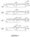
- FIGS. 4A–4Dillustrate still another embodiment of the present invention.
- FIG. 4Ashows a device 400 including a first lower layer 430 of a first dielectric material and a second upper layer 440 of a second dielectric material deposited on a substrate 410 .
- the devicealso includes a conductive element 420 embedded in the second dielectric/first dielectric/substrate composite.
- the layersare deposited and processed using conventional methods.
- the first and second materials of dielectric layers 430 , 440are selected to have different etching chemistries so that one layer is inert to etching under conditions that etch the other layer.
- Exemplary first and second dielectric materialsinclude organic dielectrics such as organic low k materials and inorganic dielectrics such as carbon-doped oxides, SiOC, fluorine-doped silicon glass (FSG), and silicon oxide-based low k materials such as Black DiamondTM available from Applied Materials, Inc., located in Santa Clara, Calif.
- the upper dielectric layer 440is an organic low k material and the lower dielectric layer 430 is a carbon-doped oxide.
- the upper and lower dielectric materialsare the same, and an intermediate surface is treated to alter the etching characteristics of the layer.
- Exemplary treatments that alter etching properties of the layerinclude inert gas plasma treatments.
- the surface treated substrateacts as an etch stop.
- the surface treatmentcan be applied in a separate step or as an integral part of the deposition process for dielectric layers.
- the deviceis processed by CMP to remove a portion of the upper dielectric layer 440 and conductive element 420 from the substrate surface.
- the dielectric layer 440has a thickness of about 100 ⁇ to about 400 ⁇ after CMP processing.
- the surfaceis then cleaned as described above, for example, with an acid bath to remove residual traces of metal on the substrate surface.
- a passivating layeris deposited on the substrate surface using electroless deposition as described herein.
- the resultant layerforms a continuous passivating layer 450 on the conductive element and random discontinuous islands 455 of passivation material on the dielectric layer 440 , as is shown in FIG. 4C .
- the deviceis then exposed to an etchant that selectively removes the remaining traces of dielectric layer 440 .
- the final deviceincludes a clean dielectric layer 430 in which a conductive metal layer 450 is embedded.
- the metallic passivating layer(and a portion of the conductive element) may extend above the plane of the substrate surface. The device is then further processed consistent with its intended function.
- One or more embodiments of the present inventionalso contemplate methods of encapsulating a conductive element using a conductive passivating layer without the need for first depositing a sacrificial protective layer.
- a conductive elementis encapsulated without stray electoless deposition of passivating metal elsewhere on the substrate surface by depositing a layer of the passivation material over the entire substrate surface or a portion thereof containing the conductive element(s), masking the passivation layer to protect the underlying conductive element(s) and removing the unmasked passivation material from the substrate surface to reveal the underlying substrate or other underlying intermediate layers.
- One or more embodiments of the present inventioncontemplate the deposition of an intermediate layer onto the substrate surface prior to deposition of the metallic passivating layer.
- the maskis subsequently removed to obtain the selectively encapsulated metal device, in which the surrounding substrate surface areas are substantially free of contaminants arising from the deposition of the passivating layer.
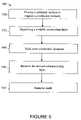
- FIG. 5is a flow chart illustrating an exemplary processing sequence 500 undertaken in encapsulating a conductive element with conductive passivating layer according to one or more embodiments of the present invention.
- a substrate surfaceis prepared as previously described by treating the substrate surface so as to expose the conductive element.
- the substrate surfacecan be treated using materials removal and cleaning techniques known in the art.
- Exemplary materials removal techniquesinclude chemical mechanical polishing (CMP) and etching.
- CMPchemical mechanical polishing
- Wet etching techniques using HF solution and dry etch techniques using HF vaporare suitable for removing dielectric materials, such as silicon oxide, from the substrate surface.
- Other etching techniquesinclude downstream or remote plasma etching using a hydrogen and water plasma or a hydrogen plasma and in situ etch processes using hydrogen, hydrogen and nitrogen or ammonia to remove metal oxides from the substrate surface.
- CMPis suitable for removal of various materials, including metals.
- Other exemplary surface treatmentsinclude ultrasonication and cleaning with an acidic solution to remove metal oxides and other contaminants from the substrate surface.
- the exposed conductive featurecan also be rinsed with distilled water to remove residual contaminants from the surface treatment process.
- a conductive passivating layerthen is deposited on the substrate surface in step 530 of FIG. 5 .
- the conductive passivation materialis generally a metal that does not form a solid solution with copper or other conductive metals, such as ruthenium, tantalum, tungsten, cobalt, palladium, nickel, tin, titanium, molybdenum, platinum, iron, and niobium and their alloys.
- the passivating conductive metalis cobalt or a cobalt alloy.
- One or more embodimentscontemplate the deposition of the conductive passivation layer as a continuous film across the substrate surface. The continuous film is deposited, for example, physical deposition techniques such as sputter deposition using a suitable target.
- the passivating layeris masked in a pattern of the underlying conducting elements.
- the passivating layercan be masked with photoresist, which is developed to remove selected areas of the photoresist film so that the underlying conductive elements are protected and the surrounding dielectric regions are exposed.
- the photoresistcan be a positive photoresist, in which case the exposed areas of a positive resist film are removed by the process of development.
- the photoresistcan be a negative photoresist, in which case the mask pattern is a negative of the underlying conductive layer structure and the unexposed areas of the resist film are removed by the process of development.
- the exposed passivating layeris then etched to selectively remove the unmasked passivating layer and to expose the underlying substrate surface.
- exemplary etching processes for removal of cobaltincludes etching at elevated temperatures, e.g., of greater than 120° C., using Cl 2 gas, and including CO, CF 4 or N 2 gas for passivation. The etching process is selective for the metallic passivation material and leaves the substrate surface free of passivation material (and other contaminants) without deleterious effect to the substrate, i.e., the dielectric regions or conductive elements of the substrate.
- the protective maskis then removed or lifted to expose the encapsulating passivating layer, as is shown in step 560 .
- Materials removal techniques known in the artcan be used. Wet etching and ashing can be used for the removal of the photoresist.
- the devicealso can be rinsed with distilled water to remove residuals from the materials removal process.
- FIGS. 6A–6Dillustrate an exemplary process for selective metal encapsulation of a conductive element according to one or more embodiments of the present invention.
- Device 600is shown in FIG. 6A having a substrate 610 containing conductive element 620 therein.
- the features of device 600illustrate only a portion of the device and the actual device may include additional layers and/or additional device features.
- the metallic conductive elementcan be prepared as previously described or according to known methods in the art.
- a thin layer 630 of passivation materialis deposited as a continuous layer on substrate surface 610 as shown in FIG. 6B , thereby encapsulating at least the conductive element 620 .
- the passivating layercan cover the entire substrate surface, or a selected region thereof; however, the deposited passivating layer should cover at least the conductive element(s).
- the passivating layercan be less than about 400 ⁇ and has a thickness in the range of about 30 ⁇ to about 300 ⁇ in some embodiments.
- the passivating layercan be deposited using physical vapor deposition techniques such as sputtering.
- a target of a composition commensurate with the desired composition of the passivating layeris bombarded with a sputtering gas, typically an inert gas, to remove atoms from the target, which are then deposited on the substrate surface.
- a sputtering gastypically an inert gas
- a suitable apparatus for sputter depositionis the EnduraTM processing system, available from Applied Materials, Inc., located in Santa Clara, Calif.
- a photoresist 640is deposited and developed as shown in FIG. 6C to mask the underlying conductive element 620 of the substrate surface.
- the photoresistcan be applied to the substrate as a spin-on layer and developed using conventional techniques.
- the surfaceis then etched as shown by arrows 650 to remove exposed passivation material 655 and to uncover the underlying regions of the substrate surface 610 .
- Exemplary etch process suitable for metals etchinginclude the use of decoupled plasma source (DPS) technology.
- Suitable apparatus for metal etching of cobalt (or other passivating metals)includes the Centura System using Metal Etch DPS processing platform, available from Applied Materials located in Santa Clara, Calif.
- the photoresist 640is lifted off to reveal passivating layer 660 and to provide a passivating layer-encapsulated conductive element 665 in which the surrounding substrate surface is substantially free of surface contaminations.
Landscapes
- Engineering & Computer Science (AREA)
- Physics & Mathematics (AREA)
- Condensed Matter Physics & Semiconductors (AREA)
- General Physics & Mathematics (AREA)
- Manufacturing & Machinery (AREA)
- Computer Hardware Design (AREA)
- Microelectronics & Electronic Packaging (AREA)
- Power Engineering (AREA)
- Internal Circuitry In Semiconductor Integrated Circuit Devices (AREA)
Abstract
Description
This application claims priority under 35 U.S.C. § 119(e) to U.S. provisional application Ser. No. 60/475,351, filed Jun. 3, 2003, which is incorporated herein by reference.
The present invention relates generally to semiconductor manufacturing, and more particularly to systems and methods for the deposition of barrier film layers on a conductive feature of the device.
A common goal in the integrated circuit (IC) industry is to place more conductive circuitry into a smaller substrate surface area. Recent improvements in circuitry of ultra-large scale integration (ULSI) on semiconductor substrates indicate that future generations of semiconductor devices will require sub-quarter micron (or less) multilevel metallization. The multilevel interconnects that lie at the heart of this technology require planarization of interconnect features formed in high aspect ratio apertures, including contacts, vias, lines and other features. One example of the use of such multilevel metallization is in “dual damascene” processing, in which two channels of conductive materials are positioned in vertically separated planes perpendicular to each other and interconnected by a vertical “via” at their closest point.
Currently, copper and its alloys have become the metals of choice for ULSI technology because copper has a lower resistivity than aluminum, (1.7 μΩ-cm compared to 3.1 μΩ-cm for aluminum), a higher current carrying capacity, and significantly higher electromigration resistance. These characteristics are important for supporting the higher current densities experienced at high levels of integration and increased device speed. Further, copper has a good thermal conductivity and is available in a highly pure state.
However, copper readily forms copper oxide when exposed to atmospheric conditions or environments outside of processing equipment. Metal oxides can result in an increase the resistance of metal layers, become a source of particle problems, and reduce the reliability of the overall circuit.
One known solution is to deposit a passivating layer or an encapsulation layer such as a dielectric material on the metal layer to prevent metal oxide formation. However, the high dielectric constant of the dielectric material increases the interlayer capacitance in multilayer environments. Furthermore, the electromigration of copper in dielectric materials is unacceptably high.
Cobalt and cobalt alloys, which are conductive (low dielectric constant) and are good barriers to electromigration of copper, have been used for passivating copper. Cobalt may be deposited by electroless deposition techniques on copper. However, copper does not satisfactorily catalyze or initiate deposition of materials from electroless solutions. It is possible to activate the copper surface to cobalt deposition by first depositing a catalytic material, such as palladium, on the copper surface. Cobalt is then selectively deposited by electroless plating onto the catalytic material. However, deposition of the catalytic material may require multiple steps or the use catalytic colloidal compounds. Catalytic colloidal compounds, and colloidal palladium materials in particular, adhere to dielectric materials and result in the undesired, excessive, and non-selective deposition of the catalyst material on the substrate surface. Alternatively, palladium can be deposited selectively on copper surfaces by a displacement mechanism in which palladium replaces a thin layer of the exposed copper on the wafer surface. However, common semiconductor fabrication methods invariably leave copper atom contaminants on the wafer surface, so that palladium is deposited on undesired locations, e.g., dielectric surfaces, as well as desired locations, e.g., conductive metal feature. In the subsequent step of cobalt deposition, cobalt is electrolessly deposited wherever palladium is present, leading to the non-selective deposition of cobalt.
Non-selective deposition of passivation material may lead to surface contamination, unwanted diffusion of conductive materials into dielectric materials, and even device failure from short circuits and other device irregularities.
There is a need for methods and systems for deposition of passivation materials that eliminate or minimize their non-selective deposition.
In one aspect of the methods and systems of the present invention, a sacrificial protective layer is used to prevent stray electroless deposition of a conductive passivating layer on a substrate surface. In one or more embodiments, the protective layer is deposited onto a substrate surface having at least one conductive element, and the protective layer is processed to expose the conductive element of the substrate surface. A conductive passivating layer is then deposited, e.g., electrolessly, on the exposed conductive element(s) of the substrate. The sacrificial protective layer prevents nucleation of the passivating layer on the substrate surface during deposition of the passivating layer. Any undesired deposition of passivation material on areas other than the conductive element(s), e.g., on the protective layer, is eliminated with the removal of the protective layer.
In one or more embodiments, the protective layer is an organic material, such as photoresist, amorphous carbon, a dielectric material, or an etch stop material. In one or more embodiments, the method includes providing one or more intermediate layers disposed between the substrate surface and the protective layer.
One or more embodiments of the present invention contemplate the deposition of an intermediate layer onto the substrate surface prior to deposition of the protective layer.
In another aspect of the invention, a method of processing a semiconductor substrate to encapsulate a conductive element is provided. The method includes the steps of depositing a metallic passivating layer onto a substrate surface comprising a conductive element, masking the passivating layer to protect the underlying conductive element of the substrate surface, etching the unmasked passivating layer to expose the underlying intermediate layers or substrate surface, and removing the mask from the passivating layer after etching.
The methods and systems of the present invention provide a semiconductor device having a conductive element selectively encapsulated by a metallic passivating layer. The passivating layer interface with the conductive element is of low capacitance. The passivating layer also provides an effective barrier to electromigration of copper into adjacent dielectric regions. Significantly, the surface of the substrate is substantially free of stray electrolessly deposited passivation material, which reduces the incidence of surface contamination, device failure from short circuit, and other device irregularities.
Various objects, features, and advantages of the present invention can be more fully appreciated with reference to the following detailed description of the invention when considered in connection with the following drawings, in which like reference numerals identify like elements. The following drawings are for the purpose of illustration only and are not intended to be limiting of the invention, the scope of which is set forth in the claims that follow.
The words and phrases used herein should be given their ordinary and customary meaning in the art by one skilled in the art unless otherwise further defined.
“Substrate surface” as used herein refers to a layer of material that serves as a basis for subsequent processing operations. For example, a substrate surface may contain one or more “conductive elements,” such as aluminum, copper, tungsten, or combinations thereof, and may form part of an interconnect feature such as a plug, via, contact, line, wire, and may also form part of a metal gate electrode. A substrate surface may also contain one or more nonconductive materials, such as silicon, doped silicon, germanium, gallium arsenide, glass, and sapphire. The substrate surface may also contain one or more low k materials such as carbon-doped oxides, porous low k materials such as organic low k and inorganic low k materials and hybrids thereof, or air-gap structures.
The term “about” is used herein to mean approximately, in the region of, roughly or around. When the term “about” is used in conjunction with a numerical range, it modifies that range by extending the boundaries above and below the numerical values set forth. In general, the term “about” is used herein to modify a numerical value above and below the stated value with a variance of 10%.
Instep 110 inFIG. 1 , a substrate surface is prepared for deposition of the passivating layer. The surface can be treated to remove surface contaminants using materials removal and/or cleaning techniques known in the art. Exemplary materials removal techniques include chemical mechanical polishing (CMP) and etching. Wet etching techniques using HF solution and dry etch techniques using HF vapor are suitable for removing dielectric materials, such as silicon oxide, from the substrate surface. Other etching techniques include downstream or remote plasma etching using a hydrogen and water plasma, or a hydrogen plasma and in situ etch processes using hydrogen, hydrogen and nitrogen, or ammonia to remove metal oxides from the substrate surface. CMP is suitable for removal of various materials, including metals and dielectric materials. Other exemplary surface treatments include ultrasonication and cleaning with an acidic solution to remove metal oxides and other contaminants from the substrate surface. The exposed conductive feature(s) can also be rinsed with distilled water to remove residual contaminants from the surface treatment process.
Instep 120 ofFIG. 1 , a sacrificial protective layer is deposited on the substrate surface. The protective layer can be any material that is compatible with the semiconductor fabrication process and that is unaffected by the subsequent deposition of a passivating layer. Exemplary materials for the protective layer include dielectrics, such as SiN, SiC, SiOC/SiC, and SiCN, photoresist, and organics such as amorphous carbon. The protective layer is deposited using known techniques such as chemical vapor deposition (CVD), plasma-enhanced chemical vapor deposition (PECVD), spin-on deposition and physical deposition processes, e.g., sputtering. The thickness of the protective layer can vary depending upon the materials used and the methods of material deposition and removal. Exemplary layer thicknesses are in the range of about 100 Å to about 5000 Å. With advances in deposition technology, such as atomic layer deposition, further reductions in film thickness are anticipated.
Instep 130 ofFIG. 1 , the protective layer is processed to remove materials above the underlying conductive element(s) so as to expose the conductive element in the underlying substrate surface. Conventional masking and materials removal techniques known in the art can be used. Etching is a common technique used for the selective removal of material. Before etching begins, a wafer is coated with photoresist and exposed to a circuit pattern (or other pattern corresponding to the conductive element) during photolithography. Etching removes material only from areas dictated by the photoresist pattern. The photoresist can be a positive photoresist, in which case the exposed areas of a positive resist film are removed by the process of development. Alternatively, the photoresist can be a negative photoresist, in which case the mask pattern is a negative of the underlying conductive layer structure and the unexposed areas of the resist film are removed by the process of development.
The exposed protective layer is then etched to selectively remove the protective layer and expose the underlying conductive element. The etching technique is selective to the material of the protective layer and can be a dry etch such as HF vapor or reactive ion etch (RIE) with CHF3/O2or plasma etch as described above. Plasma etching is performed by applying an electrical field to a gas containing a chemically reactive element, thereby generating reactive ions that can remove (etch) materials very rapidly. It also gives the chemicals an electric charge, which directs them toward the wafer vertically. This allows vertical etching profiles, which is desired in selective exposure of the features of the underlying substrate surface.
In thenext step 140, it is contemplated by one or more embodiments of the present invention that an initiation layer can be deposited on the substrate surface to initiate the electroless deposition process. The initiation layer can be a noble metal and is typically very thin, e.g., only a few monolayers thick. The initiation layer generally forms selectively on the exposed conductive element by displacement of the noble metal for the conductive metal, or can be deposited as colloidal palladium. Although the displacement process is selective for the conductive metal, there typically is some stray deposition occurring on the nonconductive surfaces, e.g., the protective layer. The substrate is then rinsed to remove the displacement solution.
A conductive passivating layer then is selectively electrolessly deposited on the initiation layer instep 150 ofFIG. 1 . The conductive material used as the passivating layer is generally a metal that does not form a solid solution with copper or other conductive metals, such as ruthenium, tantalum, tungsten, cobalt, palladium, nickel, tin, titanium, molybdenum, platinum, iron, and niobium and their alloys. In one or more embodiments, the passivating conductive metal is cobalt or a cobalt alloy. In one or more other embodiments, the passivating layer is deposited directly onto the conductive element (step150), without the need to first deposit an initiation layer (step140). Electroless deposition processes for certain cobalt alloys, using boron-containing reducing agents, permit electroless deposition of metal without the need for an initiation layer.
At least a portion of the protective layer is removed instep 160 ofFIG. 1 to remove any undesired passivation material at nucleation sites outside of the conductive element area. In one or more embodiments, a portion of the thickness of the protective layer is removed to ensure the removal of stray electroless deposition on the protective coating. In other exemplary embodiments, the entire protective layer is removed to expose the underlying layer, which may be the substrate surface or an intermediate layer.
The protective layer is removed or lifted using materials removal techniques known in the art. Exemplary, non-limiting materials removal techniques include chemical mechanical polishing (CMP), etching and ashing, e.g., plasma ashing. Reactive ion etching using CHF3/O2, wet etch techniques using HF solution, or dry etch techniques using HF vapor, are suitable for removing dielectric materials. Other etching techniques include downstream or remote plasma etching using a hydrogen and water plasma or a hydrogen plasma and in situ etch processes using hydrogen, hydrogen and nitrogen or ammonia. Wet etching and ashing can be used for the removal of carbon-containing layers, such as amorphous carbon and photoresist. The appropriate technique depends upon the composition of the material being removed. The exposed conductive feature also can be rinsed with distilled water to remove residuals from the materials removal process.
The process provides a conductive element having a conductive passivating layer selectively deposited thereon. Elsewhere, the substrate surface is free of unwanted conductive material. In exemplary embodiments, other than the deposited passivating layer, the substrate is returned to its original state prior to deposition of the passivating layer and is ready for further processing.
The electroless deposition process is described in greater detail below. Additional information regarding electroless deposition technology, generally, is found in co-pending U.S. application Ser. No. 10/117,712, entitled “Electroless Deposition Methods” and co-pending U.S. application Ser. No. 10/284,855, entitled “Post Rinse To Improve Selective Deposition Of Electroless Cobalt On Copper For ULSI Application,” both of which are commonly owned and are incorporated by reference herein.
Electroless deposition is generally defined herein as deposition of a conductive material generally provided as charged ions in a bath over an active surface to deposit the conductive material by chemical reduction in the absence of an external electric current. Electroless deposition typically involves exposing a substrate to a solution by immersing the substrate in a bath or by spraying the solution over the substrate.
In one or more embodiments, an initiation layer may be formed on the exposed conductive elements by deposition of a noble metal instep 140. Embodiments of the present invention also contemplate the use of noble metals, such as gold, silver, iridium, rhenium, rhodium, rhenium, ruthenium, palladium, platinum, osmium, and combinations thereof. In one or more embodiments, the noble metal is selected from the group of palladium, platinum, or combinations thereof. The noble metal is deposited from an activation solution containing at least a noble metal salt and an inorganic acid. Examples of noble metal salts include palladium chloride (PdCl2), palladium sulfate (PdSO4), palladium ammonium chloride, and combinations thereof. Examples of inorganic acids include hydrochloric acid (HCl), sulfuric acid (H2SO4), hydrofluoric acid (HF) and combinations thereof. Alternatively, inorganic acids, such as carboxylic acids including acetic acid (CH3COOH), may be used in the activation solution for the initiation layer.
In one or more embodiments of the present invention, displacement of the exposed conductive element, e.g., copper, by a noble metal, e.g., palladium, is carried out as follows. In a displacement plating process, wafers with an exposed copper surface are immersed in a bath containing dissolved ions of a metal more noble than copper. With simple immersion, the copper dissolves, i.e., is oxidized, and a film of the more noble metal deposits, i.e., is reduced, to thereby displace atoms of copper with the noble metal. Displacement is selective to copper and the coating thickness is self-limiting. Depending on the porosity of the copper, the noble metal may be up to a few monolayers thick.
The noble metal salt may be in the deposition solution at a concentration between about 20 parts per million (ppm) and about 20 g/liter. The concentration of the metal salt may also be described as a volume percent with 1 vol % corresponding to about 40 ppm. The inorganic acid is used to provide an acidic deposition composition, for example, at a pH of about 7 or less. A pH level between about 1 and about 3 has been observed to be effective in displacement deposition of the noble metals from the activation solution. An acidic solution has also been observed to be effective in removing or reducing oxides, such as metal oxides including copper oxides, from the metal or dielectric surface of the substrate during the activation deposition process.
The activation solution for the initiation layer is generally applied to the substrate surface for between about 1 second and about 300 seconds at a composition temperature between about 15° C. and about 80° C. The activation solution is generally provided at a flow rate between about 50 ml/min and about 2000 ml/min. In one aspect a total application of about 120 ml and about 200 ml of activation solution was provided to deposit the activation layer. The activation solution generally provides for the deposition of a noble metal to a thickness of about 50 Å or less, such as about 10 Å or less. The initiation layer may be continuous or discontinuous.
An example of an activation solution composition for depositing the initiation material includes about 3 vol % (120 ppm) of palladium chloride and sufficient hydrochloric acid to provide a pH of about 1.5 for the composition, which is applied to the substrate surface for about 30 seconds at a flow rate of about 750 ml/min at a composition temperature of about 25° C.
In other embodiments, the initiation layer is formed by exposing the exposed conductive materials to a borane-containing composition instep 140. The borane-containing composition forms a metal boride layer selectively on the exposed conductive metals, which provides catalytic sites for subsequent electroless deposition processes.
The borane-containing composition includes a borane reducing agent. Suitable borane-containing reducing agents include alkali metal borohydrides, alkyl amine boranes, and combinations thereof. Examples of suitable borane-containing reducing agents include sodium borohydride, dimethylamine borane (DMAB), trimethylamine borane, and combinations thereof. The borane-containing reducing agent comprises between about 0.25 grams per liter (g/L) and about 6 g/L of the boron-containing composition. The borane-containing composition may additionally include pH-adjusting agents to provide a pH of between about 8 and about 13. Suitable pH adjusting agents include potassium hydroxide (KOH), sodium hydroxide (NaOH), ammonium hydroxide, ammonium hydroxide derivatives, such as tetramethyl ammonium hydroxide, and combinations thereof.
The conductive element is generally exposed to the borane-containing composition between about 30 seconds and about 180 seconds at a composition temperature between about 15° C. and about 80° C. The borane-containing composition may be delivered to the substrate at a flow rate between about 50 ml/min and about 2000 ml/min. In one aspect a total application of about 120 ml and about 200 ml of the borane-containing composition was provided to form the initiation layer of a metal boride compound.
An example of a borane-containing composition for forming the layer includes about 4 g/L of dimethylamine borane (DMAB) and sufficient sodium hydroxide to provide a pH of about 9 for the composition, which is generally applied to the substrate surface for about 30 seconds at a flow rate of about 750 ml/min at a composition temperature of about 25° C.
A rinsing agent, typically deionized water, is then applied to the substrate surface to remove any solution used in forming the initiation layer.
A metallic passivating layer is deposited by an electroless process on the initiation layer instep 150. In one or more embodiments of the present invention, the metal passivating layer comprises cobalt or a cobalt alloy. Cobalt alloys include cobalt-tungsten alloy, cobalt-phosphorus alloy, cobalt-tin alloys, cobalt-boron alloys, including ternary alloys, such as cobalt-tungsten-phosphorus and cobalt-tungsten-boron. One or more embodiments of the present invention also contemplate the use of other materials, including nickel, tin, titanium, tantalum, tungsten, molybdenum, platinum, iron, niobium, palladium, platinum, and combinations thereof, and other alloys including nickel cobalt alloys, doped cobalt and doped nickel alloys, or nickel iron alloys, to form the metal layer as described herein.
In one or more embodiments of the present invention, the metallic passivation material is deposited from an electroless solution containing at least a metal salt and a reducing agent. The electroless solution may further include additives to improve deposition of the metal. Additives may include surfactants, complexing agents, pH adjusting agents, or combinations thereof.
Suitable metal salts include chlorides, sulfates, sulfamates, or combinations thereof. An example of a metal salt is cobalt chloride. The metal salt may be in the electroless solution at a concentration between about 0.5 g/L and about 30 g/L.
Cobalt alloys, such as cobalt-tungsten may be deposited by adding tungstic acid or tungstate salts including sodium tungstate, and ammonium tungstate, and combinations thereof for tungsten deposition. Phosphorus for the cobalt-tungsten-phosphorus deposition may be formed by phosphorus-containing reducing agents, such as hypophosphite. Cobalt alloys, such as cobalt-tin may be deposited by adding stannate salts including stannic sulfate, stannic chloride, and combinations thereof. The additional metals salts, for example, for tungsten and tin, may be in the electroless solution at a concentration between about 0.5 g/L and about 30 g/L.
Suitable reducing agents include sodium hypophosphite, hydrazine, formaldehyde, and combinations thereof. The reducing agents have a concentration between about 1 g/L and about 30 g/L of the electroless solution. For example, hypophosphite may be added to the electroless solution at a concentration between about 15 g/L and about 30 g/L.
The reducing agents may also include borane-containing reducing agents, such as sodium borohydride, dimethylamine borane (DMAB), trimethylamine borane, and combinations thereof. The borane-containing reducing agent comprises between about 0.25 grams per liter (g/L) and about 6 g/L of the boron-containing composition. The presence of borane-containing reducing agents allow for the formation of cobalt-boron alloys such as cobalt-tungsten-boron and cobalt-tin-boron among others.
The metal electroless solutions described herein are generally applied to the substrate surface for between about 30 seconds and about 180 seconds at a composition temperature between about 60° C. and about 90° C. The electroless solution is generally provided at a flow rate between about 50 ml/min and about 2000 ml/min. In one embodiment of the present invention, a total application of between about 120 ml and about 200 ml of electroless solution was provided to deposit the electroless layer. The electroless solution generally provides for the deposition of a metal layer to a thickness of about 500 Å or less, such as between about 300 Å and about 400 Å.
An example of a cobalt electroless composition for forming a cobalt layer includes about 20 g/L of cobalt sulfate, about 50 g/L of sodium citrate, about 20 g/L of sodium hypophosphite, with sufficient potassium hydroxide to provide a pH of between about 9 and about 11 for the composition, which is applied to the substrate surface for about 120 seconds at a flow rate of about 750 ml/min at a composition temperature of about 80° C. A cobalt-tungsten layer is deposited by the addition of about 10 g/L of sodium tungstate.
An example of a cobalt electroless composition for forming a cobalt layer with a borane-containing reducing agent includes about 20 g/L of cobalt sulfate, about 50 g/L of sodium citrate, about 4 g/L of dimetylamineborane, with sufficient potassium hydroxide to provide a pH of between about 10 and about 12 for the composition, which is applied to the substrate surface for about 120 seconds at a flow rate of about 750 ml/min at a composition temperature of about 80° C. A cobalt-tungsten-boron layer is deposited by the addition of about 10 g/L of sodium tungstate.
Borane-containing reducing agents in the metal electroless deposition process allow electroless deposition on exposed conductive material without the need for an initiation layer. When an initiation layer is first deposited on the substrate surface prior to the metal electroless deposition, the process is typically performed in two processing chambers. When the metal electroless deposition process occurs without the initiation layer, such as with the use of borane-containing reducing agents in the metal electroless deposition, the electroless process can be performed in one chamber.
Additionally, the method of depositing the material from an electroless solution, whether the initiation layer or metal layer, may include applying a bias to a conductive portion of the substrate structure if available (i.e. a seed layer), such as a DC bias, during the electroless deposition process.
The initiation layer and/or metal passivating layer may be annealed (i.e., heated) at a temperature between about 100° C. to about 400° C. The anneal may be performed in a vacuum or in a gas atmosphere, such as a gas atmosphere of one or more noble gases (such as Argon, Helium), nitrogen, hydrogen, and mixtures thereof.
Suitable apparatus for performing electroless deposition processes include an Electra Cu™ ECP processing platform or Link™ processing platform that are commercially available from Applied Materials, Inc., located in Santa Clara, Calif. The Electra Cu™ ECP platform, for example, includes an integrated processing chamber capable of depositing a conductive material by an electroless process, such as an electroless deposition processing (EDP) cell, which is commercially available from Applied Materials, Inc., located in Santa Clara, Calif. The Electra Cu™ ECP platform generally includes one or more electroless deposition processing (EDP) cells as well as one or more pre-deposition or post-deposition cell, such as spin-rinse-dry (SRD) cells, etch chambers, or annealing chambers.
Suitable apparatus for deposition of dielectric films are the Producer™ CVD and PECVD systems, available from Applied Materials, Inc., located in Santa Clara, Calif. The Producer™ systems use a multichamber architecture in a design that transfers wafers in pairs to process modules; each module has two identical chambers that use common vacuum and gas delivery subsystems. In addition to handling the full range of conventional dielectric CVD and PECVD applications, the Producer™ system deposits DARC™, damascene nitride and low k films such as TEOS FSG, Black Diamond™ and BLOk™ (Barrier Low k).
Etching processes, including dry etch and plasma etch, can be carried out on an eMax™ etching system available from Applied Materials, Inc., located in Santa Clara, Calif. The system includes a low pressure/high gas flow regime, controllable magnetic field, and high rf power capability. The eMax™ system integrates etch, photoresist strip and barrier removal steps on a single system. Etch rates of over 6000 angstroms/min. is possible. Wet etch or wet cleaning processes can be accomplished on an Oasis Clean™ system, also available from Applied Materials, Inc., CA. The apparatus uses both ultrasonic cleaning and wet chemical cleaning processes to clean substrate surfaces.
A suitable integrated controller and polishing apparatus is the Mirra™ with iAPC or Mirra Mesa™ with iAPC, also available from Applied Materials, Inc., CA.
The metallic conductive element is formed in the substrate using, for example, selective electroless metallization, in which the conductive metal is catalytically deposited from a metal ion solution without the application of an electrical current. Because the conductive metals, and copper in particular, tend to diffuse into adjacent dielectric materials such as SiO2, it is common practice to line the viaopening 220 with a diffusion barrier layer (not shown) such as titanium nitride, titanium tungsten, tantalum, tantalum nitride and tungsten nitride. In addition, the diffusion barrier layer is activated, for example by the deposition of a seed layer of palladium or displacement reaction with copper, to promote the autocatalytic deposition of copper. Other methods of metallic deposition include physical vapor deposition methods such as sputter deposition from the appropriate target. CMP techniques are used to polish away unwanted conductive metal and to prepare the substrate for deposition of the passivating layer.
The surface can be further treated to clean the substrate surface of contaminants using techniques known in the art. Wet etching techniques using HF solution and dry etch techniques using HF vapor are suitable for removing dielectric materials, such as silicon oxide, from the substrate surface. Other etching techniques include downstream or remote plasma etching using a hydrogen and water plasma or a hydrogen plasma and in situ etch processes using hydrogen, hydrogen and nitrogen, or ammonia to remove metal oxides from the substrate surface. CMP is suitable for removal of various materials, including metals and dielectric materials. Other exemplary surface treatments include cleaning with an acidic solution to remove metal oxides and other contaminants from the substrate surface. The exposed conductive feature can also be rinsed with distilled water to remove residual contaminants from the surface treatment process.
After substrate surface preparation, a sacrificialprotective layer 230 is deposited on the substrate surface, as is illustrated inFIG. 2B . The protective layer can be deposited by any method that is compatible with the device fabrication process and can be made up of any material that can be incorporated into the device fabrication process without detriment to the subsequent processing steps.
In exemplary embodiments, the protective layer is a photoresist, which can be applied to the substrate as a spin-on layer at a thickness of about 1000 Å to about 5000 Å. Subsequently, the photoresist is exposed and developed to define one ormore openings 240 that provides access to the underlying conductive element(s)220, as is shown inFIG. 2C . Athin layer 250 of passivation material is deposited onconductive element 220 by electroless deposition as described above and as shown inFIG. 2D . The passivating layer can be less than about 400 Å and can have a thickness in the range of about 30 Å to about 300 Å in at least some embodiments. The passivating layer may be deposited in two steps by first depositing an initiation layer, followed by depositing a conductive passivating layer. Alternatively, the passivating layer may be deposited in a single step directly onto the conductive element. Regardless of the method of passivating layer deposition,random nucleation sites 255 of the passivating metal also form on theprotective layer 230. In a subsequent step shown inFIG. 2E , thephotoresist 230 is lifted off of the substrate surface so thatunwanted nucleation sites 255 are removed and thepassivating layer 250 remains only on theconductive element 220. The photoresist is removed by conventional processes, such as wet etch or ashing, that is selected to remove the photoresist without negative effect on the underlying intermediate layer(s) or substrate surface. The substrate can be cleaned using wet solvent that does not dissolve the passivating layer. The device is then further processed consistent with its intended function.
The above procedure is attractive because it does not require the use of a high k dielectric material adjacent to the conductive element. Low k materials, e.g., polyarylethers, fluorinated polyarylethers, polyimides and fluorinated polyimides, benzocyclobutenes, carbon-doped oxides, organic and inorganic porous low k materials and hybrids thereof, and the like, can be directly applied to the substrate surface after completion of the processing steps set forth inFIGS. 2A–2E to provide improved electrical isolation between adjacent conductive regions of an integrated circuit that is advantageous in many semiconductor devices.
In another exemplary embodiment, theprotective layer 230 is a dielectric barrier layer such as an etch stop layer. Exemplary etch stop materials include SiN or SiOC available from Applied Materials, Inc., located in Santa Clara, Calif., under the tradename Blok™. The etch stop layer (or other dielectric) is deposited as a thin layer, e.g., about 50 Å, over the substrate surface by, for example, PECVD or spin-on polymer deposition. Alternatively, a thick layer of dielectric material is deposited and is etched or polished back to a very thin protective layer, for example about 50 Å. The thinness of the protective layer is chosen to reduce the amount of high k material deposited on the metallic conductive element and thereby reduce interlayer capacitance. The conductive element is exposed by removing, i.e., etching, the dielectric layer in those areas not protected by a photomask (not shown) to define one ormore openings 240 that exposes the underlyingconductive element 220, as is shown inFIG. 2C . Apassivating layer 250 is deposited as described above. The dielectric barrier (protecting layer) or at least a portion of the protecting layer is then removed along with surface contaminates255. In one or more other exemplary embodiments, only a portion of the dielectric layer is removed (sufficient to remove stray electrolessly deposited sites255), and additional dielectric material is deposited on the remaining dielectric layer to a final thickness. The final thickness is desirably low to minimize the effects of the high k material, and can be in the range of about 600 Å. The device is then further processed consistent with its intended function.
In another embodiment of the present invention, theprotective layer 230 is an amorphous carbon layer. In one or more embodiments, the amorphous carbon layer is deposited onto the substrate surface, for example, by CVD or spin-on polymer deposition to a thickness of about 100 Å to about 5000 Å. The conductive element is exposed by masking the amorphous carbon film and developing the photoresist to expose the underlying amorphous carbon film. The carbon film is then removed, e.g., by etching, in those areas not protected by the photomask (not shown) to define one ormore openings 240 that exposes the underlying conductive element(s)220, as is shown inFIG. 2C . Apassivating layer 250 is deposited as described above. The amorphous carbon layer is then removed along with surface contaminates255 to eliminate stray electrolessly deposited passivation material (and other contaminants). Amorphous carbon can be removed by ashing, plasma ashing and wet or dry chemical etching. As with the use of a photoresist, the process results in the complete removal of the amorphous carbon film, so that no high k dielectric material remains adjacent to the conductive elements. The device is then further processed consistent with its intended function.
In another exemplary embodiment of the present invention, intermediate layers may be deposited between the substrate surface and the protective layer.FIGS. 3A–3F illustrate an exemplary process for such an integration scheme using a conductive passivating layer.Device 300 is shown inFIG. 3A having asubstrate 310 containing aconductive element 320 therein. As noted above, the features ofdevice 300 represent only a portion of the device and the actual device may include additionally layers and/or additional device features.
A sacrificialprotective layer 330 is deposited on the substrate surface, as is illustrated inFIG. 3B . Prior to deposition of the protective layer, one or more intermediate layer(s)335 is deposited on the substrate surface. The protective and intermediate layers can be any of the materials and layers described above, and can be deposited according to any of the method described herein or any other conventional technique. In an exemplary embodiment, the protective layer is a photoresist and the intermediate layer is a dielectric material such as an etch stop.
As is shown inFIG. 3B ,dielectric material 335 is deposited over thesubstrate surface 310, e.g., by PECVD or spin-on polymer deposition, to a thickness of about 50 to about 1000 Å. Aphotoresist layer 330 then is applied to the intermediate layer as a spin-on layer at a thickness of about 1000 Å to about 5000 Å. Subsequently, the photoresist is exposed and developed to define one ormore openings 340 that exposes the underlyingintermediate layer 335 above theconductive element 320, as is shown inFIG. 3C . The conductive element is exposed by removing, i.e., etching, the dielectric layer in those areas not protected by aprotective layer 330 to define one ormore openings 345 that exposes the underlyingconductive element 320, as is shown inFIG. 3D . In one or more embodiments of the present invention, the etch is selective for theintermediate layer 335, so thatprotective layer 330 is not affected by the etch process. In one or more embodiments, the photomask is removed only after etching of both the protective and intermediate layers.
Athin layer 350 of passivation material is deposited onconductive element 320 by electroless deposition as described above and as shown inFIG. 3E . The passivating layer can be less than about 400 Å, and has a thickness in the range of about 30 Å to about 300 Å in exemplary embodiments. Thepassivating layer 350 can be of the same or different thickness as thedielectric layer 335. The passivating layer may be deposited in two steps by depositing an initiation layer, followed by depositing the conductive passivating layer. Alternatively, the passivating layer may be deposited in a single step directly onto the conductive element. Regardless of the method of passivating layer deposition,random nucleation sites 355 of the passivating metal also form on the protective layer. In a subsequent step shown inFIG. 3F , the protective layer330 (e.g., photoresist), includingunwanted nucleation sites 355, is lifted off of the substrate surface, leaving thepassivating layer 350 only on theconductive element 320. The photoresist is removed by conventional processes, such as wet etch or ashing, that is selected to remove the photoresist without negative effect on the underlying dielectric materials of the intermediate layer(s) or substrate surface. Upon removal of the photoresist layer,dielectric layer 335 covers the remaining surface of thesubstrate 310. In those embodiments where thedielectric layer 335 and thepassivating layer 350 are of the same thickness, a smooth planar substrate surface containing the passivating layer embedded in a dielectric is obtained, as illustrated inFIG. 3F . The substrate can be cleaned using wet solvent that does not dissolve the passivating layer. The device is then further processed consistent with its intended function.
Referring toFIG. 4B , the device is processed by CMP to remove a portion of theupper dielectric layer 440 andconductive element 420 from the substrate surface. In an exemplary embodiment, thedielectric layer 440 has a thickness of about 100 Å to about 400 Å after CMP processing. The surface is then cleaned as described above, for example, with an acid bath to remove residual traces of metal on the substrate surface. Subsequently, a passivating layer is deposited on the substrate surface using electroless deposition as described herein. The resultant layer forms acontinuous passivating layer 450 on the conductive element and randomdiscontinuous islands 455 of passivation material on thedielectric layer 440, as is shown inFIG. 4C . The device is then exposed to an etchant that selectively removes the remaining traces ofdielectric layer 440. The final device includes aclean dielectric layer 430 in which aconductive metal layer 450 is embedded. In one or more embodiments, the metallic passivating layer (and a portion of the conductive element) may extend above the plane of the substrate surface. The device is then further processed consistent with its intended function.
One or more embodiments of the present invention also contemplate methods of encapsulating a conductive element using a conductive passivating layer without the need for first depositing a sacrificial protective layer. According to one or more embodiments of the present invention, a conductive element is encapsulated without stray electoless deposition of passivating metal elsewhere on the substrate surface by depositing a layer of the passivation material over the entire substrate surface or a portion thereof containing the conductive element(s), masking the passivation layer to protect the underlying conductive element(s) and removing the unmasked passivation material from the substrate surface to reveal the underlying substrate or other underlying intermediate layers. One or more embodiments of the present invention contemplate the deposition of an intermediate layer onto the substrate surface prior to deposition of the metallic passivating layer. The mask is subsequently removed to obtain the selectively encapsulated metal device, in which the surrounding substrate surface areas are substantially free of contaminants arising from the deposition of the passivating layer.
Instep 510 inFIG. 5 , a substrate surface is prepared as previously described by treating the substrate surface so as to expose the conductive element. The substrate surface can be treated using materials removal and cleaning techniques known in the art. Exemplary materials removal techniques include chemical mechanical polishing (CMP) and etching. Wet etching techniques using HF solution and dry etch techniques using HF vapor are suitable for removing dielectric materials, such as silicon oxide, from the substrate surface. Other etching techniques include downstream or remote plasma etching using a hydrogen and water plasma or a hydrogen plasma and in situ etch processes using hydrogen, hydrogen and nitrogen or ammonia to remove metal oxides from the substrate surface. CMP is suitable for removal of various materials, including metals. Other exemplary surface treatments include ultrasonication and cleaning with an acidic solution to remove metal oxides and other contaminants from the substrate surface. The exposed conductive feature can also be rinsed with distilled water to remove residual contaminants from the surface treatment process.
A conductive passivating layer then is deposited on the substrate surface instep 530 ofFIG. 5 . The conductive passivation material is generally a metal that does not form a solid solution with copper or other conductive metals, such as ruthenium, tantalum, tungsten, cobalt, palladium, nickel, tin, titanium, molybdenum, platinum, iron, and niobium and their alloys. In one or more embodiments, the passivating conductive metal is cobalt or a cobalt alloy. One or more embodiments contemplate the deposition of the conductive passivation layer as a continuous film across the substrate surface. The continuous film is deposited, for example, physical deposition techniques such as sputter deposition using a suitable target.
Instep 540 ofFIG. 5 , the passivating layer is masked in a pattern of the underlying conducting elements. The passivating layer can be masked with photoresist, which is developed to remove selected areas of the photoresist film so that the underlying conductive elements are protected and the surrounding dielectric regions are exposed. The photoresist can be a positive photoresist, in which case the exposed areas of a positive resist film are removed by the process of development. Alternatively, the photoresist can be a negative photoresist, in which case the mask pattern is a negative of the underlying conductive layer structure and the unexposed areas of the resist film are removed by the process of development.
Instep 550 ofFIG. 5 , the exposed passivating layer is then etched to selectively remove the unmasked passivating layer and to expose the underlying substrate surface. Exemplary etching processes for removal of cobalt includes etching at elevated temperatures, e.g., of greater than 120° C., using Cl2gas, and including CO, CF4or N2gas for passivation. The etching process is selective for the metallic passivation material and leaves the substrate surface free of passivation material (and other contaminants) without deleterious effect to the substrate, i.e., the dielectric regions or conductive elements of the substrate.
The protective mask is then removed or lifted to expose the encapsulating passivating layer, as is shown instep 560. Materials removal techniques known in the art can be used. Wet etching and ashing can be used for the removal of the photoresist. The device also can be rinsed with distilled water to remove residuals from the materials removal process.
Athin layer 630 of passivation material is deposited as a continuous layer onsubstrate surface 610 as shown inFIG. 6B , thereby encapsulating at least theconductive element 620. The passivating layer can cover the entire substrate surface, or a selected region thereof; however, the deposited passivating layer should cover at least the conductive element(s). The passivating layer can be less than about 400 Å and has a thickness in the range of about 30 Å to about 300 Å in some embodiments. The passivating layer can be deposited using physical vapor deposition techniques such as sputtering. In sputtering, a target of a composition commensurate with the desired composition of the passivating layer is bombarded with a sputtering gas, typically an inert gas, to remove atoms from the target, which are then deposited on the substrate surface. A suitable apparatus for sputter deposition is the Endura™ processing system, available from Applied Materials, Inc., located in Santa Clara, Calif.
Aphotoresist 640 is deposited and developed as shown inFIG. 6C to mask the underlyingconductive element 620 of the substrate surface. The photoresist can be applied to the substrate as a spin-on layer and developed using conventional techniques. The surface is then etched as shown byarrows 650 to remove exposedpassivation material 655 and to uncover the underlying regions of thesubstrate surface 610. Exemplary etch process suitable for metals etching include the use of decoupled plasma source (DPS) technology. Suitable apparatus for metal etching of cobalt (or other passivating metals) includes the Centura System using Metal Etch DPS processing platform, available from Applied Materials located in Santa Clara, Calif.
In a subsequent step shown inFIG. 6D , thephotoresist 640 is lifted off to revealpassivating layer 660 and to provide a passivating layer-encapsulatedconductive element 665 in which the surrounding substrate surface is substantially free of surface contaminations.
Although various embodiments that incorporate the teachings of the present invention have been shown and described in detail herein, those skilled in the art can readily devise many other varied embodiments that incorporate these teachings, including embodiments with numerical values and ranges differing from those set forth herein. It is appreciated that the figures and discussion herein illustrate only a portion of an exemplary semiconductor device. Thus, the present invention is not limited to only those structures described herein.
Claims (33)
1. A method of processing a semiconductor substrate, comprising the steps of:
depositing a protective layer on a topographically substantially flat substrate surface comprising an exposed conductive element;
selectively removing a portion of the protective layer to expose the conductive element of the substrate surface;
selectively electrolessly depositing a metallic passivating layer onto the exposed conductive element, wherein discontinuous regions of stray metallic passivating material are also deposited on the protective layer; and
removing at least a portion of the protective layer from the substrate after deposition of the metallic passivating layer, wherein the stray metallic passivating material deposited on the protective layer is also removed.
2. The method ofclaim 1 , wherein the substrate surface comprises a dielectric material in which the conductive element is disposed.
3. The method ofclaim 1 , wherein the substrate surface comprises a low k dielectric material.
4. The method ofclaim 1 , wherein a portion of the thickness of the protective layer is removed.
5. The method ofclaim 1 , wherein the entire thickness of the protective layer is removed.
6. The method ofclaim 1 , wherein the step of depositing a protective layer is accomplished using a technique selected from the group consisting of chemical vapor deposition (CVD), plasma enhance chemical vapor deposition (PECVD), spin on deposition and physical vapor deposition.
7. The method ofclaim 1 , wherein the protective layer comprises an organic material.
8. The method ofclaim 7 , wherein the organic material of the layer is selected from the group consisting of photoresist and amorphous carbon.
9. The method ofclaim 8 , wherein the steps of depositing and processing the photoresist protective layer comprise the steps of:
depositing a photoresist over the substrate surface; and
exposing and developing the photoresist under conditions that do not degrade the substrate surface to expose a selected region of an underlying layer.
10. The method ofclaim 9 , wherein the exposed and developed photoresist is removed after deposition of the metallic passivating layer by ashing or wet chemical etch.
11. The method ofclaim 8 , wherein the steps of depositing and processing the amorphous carbon protective layer comprise the steps of:
depositing an amorphous carbon layer over the substrate surface; and
etching the amorphous carbon layer under conditions that do not degrade the substrate surface.
12. The method ofclaim 11 , wherein the amorphous carbon layer is removed after deposition of the metallic passivating layer by ashing or reactive ion etch.
13. The method ofclaim 1 , wherein the protective layer comprises a dielectric material.
14. The method ofclaim 13 , wherein steps of depositing and processing the dielectric protective layer comprise the steps of:
depositing a dielectric layer over the substrate surface; and
selectively etching the dielectric layer under conditions that do not degrade the substrate surface.
15. The method ofclaim 14 , wherein the dielectric protective layer is removed after deposition of the passivating layer by etching using a technique selected from the group consisting of wet etch, dry etch, reactive ion etch and plasma etch.
16. The method ofclaim 1 , where steps for depositing and processing the protective layer comprise the steps of:
depositing an intermediate layer on the substrate surface;
depositing a protective layer on the intermediate layer;
selectively removing the protective layer to expose the intermediate layer; and
selectively removing the intermediate layer under conditions that do not degrade the conductive element.
17. The method ofclaim 16 , wherein the intermediate layer comprises an etch stop and the protective layer comprises a photoresist.
18. The method ofclaim 16 , wherein the intermediate layer comprises a dielectric material.
19. The method ofclaim 1 , wherein the conductive material comprises copper.
20. The method ofclaim 1 , wherein the passivating layer is selected from the group consisting of ruthenium, tantalum, tungsten, cobalt, palladium, nickel, tin, titanium, molybdenum, platinum, iron, and niobium, and alloys thereof.
21. The method ofclaim 1 , wherein the step of electrolessly depositing a metallic passivating layer comprises the steps of:
depositing an initiation layer on the first conductive material by exposing the substrate to an activation solution;
cleaning the substrate after deposition of the initiation layer; and
depositing a metallic passivating layer on the initiation layer by exposing the initiation layer to an electroless solution.
22. A method of processing a semiconductor substrate, comprising:
steps for depositing a protective layer on a topographically substantially flat substrate surface comprising an exposed conductive element disposed in a dielectric material;
steps for processing the protective layer to expose the conductive element;
steps for selectively electrolessly depositing a metallic passivating layer onto the conductive element, wherein discontinuous regions of stray metallic passivating material are also deposited on the protective layer; and
steps for removing at least a portion of the protective layer from the substrate after electroless deposition, wherein the stray metallic passivating material deposited on the protective layer is also removed.
23. The method ofclaim 22 , wherein the step of depositing a metallic passivating layer comprises the steps of:
steps for depositing an initiation layer on the first conductive material by exposing the substrate to an activation solution;
steps for cleaning the substrate after deposition of the initiation layer; and
steps for depositing a metallic passivating layer on the initiation layer by exposing the initiation layer to an electroless solution.
24. The method ofclaim 22 , where steps for depositing and processing the protective layer comprise the steps of:
steps for depositing an intermediate layer on the substrate surface;
steps for depositing a protective layer on the intermediate layer;
steps for exposing and developing the protective layer to expose the intermediate layer; and
steps for etching the intermediate layer under conditions that do not degrade the conductive element.
25. The method ofclaim 22 , wherein steps for depositing and processing an amorphous carbon protective layer comprise the steps of:
steps for depositing an amorphous carbon layer over the substrate surface; and
steps for etching the amorphous carbon layer under conditions that do not degrade the conductive element.
26. The method ofclaim 22 , wherein the steps for depositing and processing a photoresist protective layer comprise the steps of:
steps for depositing a photoresist over the substrate surface; and
steps for exposing and developing the photoresist under conditions that do not degrade the conductive element.
27. The method ofclaim 22 , wherein the steps of depositing and processing a dielectric protective layer comprise the steps of:
steps for depositing a dielectric protective layer over the substrate surface; and
steps for etching the dielectric protective layer under conditions that do not degrade the conductive element.
28. A system for processing a semiconductor substrate, comprising:
means for depositing a protective layer on a topographically substantially flat substrate surface comprising an exposed conductive element disposed in a dielectric material;
means for processing the protective layer to expose the conductive element;
means for selectively electrolessly depositing a metallic passivating layer onto the conductive element, wherein discontinuous regions of stray metallic passivating material are also deposited on the protective layer; and
means for removing at least a portion of the protective layer from the substrate after electroless deposition, and for removing the stray metallic passivating material deposited on the protective layer.
29. The system ofclaim 28 , wherein the steps for depositing and processing a photoresist protective layer comprises the steps of:
means for depositing a photoresist over the substrate surface; and
means for exposing and developing the photoresist under conditions that do not degrade the conductive element.
30. The system ofclaim 28 , wherein the step of electrolessly depositing a metallic passivating layer comprises the steps of:
means for depositing an initiation layer on the first conductive material by exposing the substrate to an activation solution;
means for cleaning the substrate after deposition of the initiation layer; and
steps for depositing a metallic passivating layer on the initiation layer by exposing the initiation layer to an electroless solution.
31. The system ofclaim 26 , where steps for depositing and processing the protective layer comprises the steps of:
means for depositing an intermediate layer on the substrate surface;
means for depositing a protective layer on the intermediate layer;
means for exposing and developing the protective layer to expose the intermediate layer; and
means for etching the intermediate layer under conditions that do not degrade the conductive element.
32. The system ofclaim 26 , wherein steps for depositing and processing an amorphous carbon protective layer comprises the steps of:
means for depositing an amorphous carbon layer over the substrate surface; and
means for etching the amorphous carbon layer under conditions that do not degrade the conductive element.
33. The system ofclaim 26 , wherein depositing and processing a dielectric protective layer comprises:
means for depositing a dielectric layer over the substrate surface; and
means for etching the dielectric layer under conditions that do not degrade the conductive element.
Priority Applications (1)
| Application Number | Priority Date | Filing Date | Title |
|---|---|---|---|
| US10/812,480US7205228B2 (en) | 2003-06-03 | 2004-03-30 | Selective metal encapsulation schemes |
Applications Claiming Priority (2)
| Application Number | Priority Date | Filing Date | Title |
|---|---|---|---|
| US47535103P | 2003-06-03 | 2003-06-03 | |
| US10/812,480US7205228B2 (en) | 2003-06-03 | 2004-03-30 | Selective metal encapsulation schemes |
Publications (2)
| Publication Number | Publication Date |
|---|---|
| US20040248409A1 US20040248409A1 (en) | 2004-12-09 |
| US7205228B2true US7205228B2 (en) | 2007-04-17 |
Family
ID=33493413
Family Applications (1)
| Application Number | Title | Priority Date | Filing Date |
|---|---|---|---|
| US10/812,480Expired - Fee RelatedUS7205228B2 (en) | 2003-06-03 | 2004-03-30 | Selective metal encapsulation schemes |
Country Status (1)
| Country | Link |
|---|---|
| US (1) | US7205228B2 (en) |
Cited By (27)
| Publication number | Priority date | Publication date | Assignee | Title |
|---|---|---|---|---|
| US20060249849A1 (en)* | 2004-06-18 | 2006-11-09 | Uri Cohen | Methods and structures for interconnect passivation |
| US20070281534A1 (en)* | 2006-06-05 | 2007-12-06 | Hon Hai Precision Ind. Co., Ltd. | Electrical connector |
| US20080236619A1 (en)* | 2007-04-02 | 2008-10-02 | Enthone Inc. | Cobalt capping surface preparation in microelectronics manufacture |
| US20080254639A1 (en)* | 2005-10-31 | 2008-10-16 | Novellus Systems, Inc. | Method for etching organic hardmasks |
| US20090117731A1 (en)* | 2007-11-01 | 2009-05-07 | Taiwan Semiconductor Manufacturing Co., Ltd. | Semiconductor interconnection structure and method for making the same |
| US20090138114A1 (en)* | 2005-05-11 | 2009-05-28 | Richard Gerard Burda | Method of release and product flow management for a manufacturing facility |
| US20100044865A1 (en)* | 2006-11-29 | 2010-02-25 | Nxp B.V. | Fabrication of a diffusion barrier cap on copper containing conductive elements |
| US20110053349A1 (en)* | 2009-08-31 | 2011-03-03 | Semiconductor Manufacturing International (Shanghai) Corporation | Application of millisecond heating source for surface treatment |
| US20110065281A1 (en)* | 2009-09-11 | 2011-03-17 | Semiconductor Manufacturing International (Shanghai) Corporation | Method of rapid thermal treatment using high energy electromagnetic radiation of a semiconductor substrate for formation of epitaxial materials |
| US20110190921A1 (en)* | 2010-02-02 | 2011-08-04 | Applied Materials, Inc. | Flexible process condition monitoring |
| US8420531B2 (en) | 2011-06-21 | 2013-04-16 | International Business Machines Corporation | Enhanced diffusion barrier for interconnect structures |
| US8664124B2 (en) | 2005-10-31 | 2014-03-04 | Novellus Systems, Inc. | Method for etching organic hardmasks |
| US8962101B2 (en) | 2007-08-31 | 2015-02-24 | Novellus Systems, Inc. | Methods and apparatus for plasma-based deposition |
| US9023731B2 (en) | 2012-05-18 | 2015-05-05 | Novellus Systems, Inc. | Carbon deposition-etch-ash gap fill process |
| US9240320B1 (en) | 2008-06-27 | 2016-01-19 | Novellus Systems, Inc. | Methods of depositing smooth and conformal ashable hard mask films |
| US9304396B2 (en) | 2013-02-25 | 2016-04-05 | Lam Research Corporation | PECVD films for EUV lithography |
| US9320387B2 (en) | 2013-09-30 | 2016-04-26 | Lam Research Corporation | Sulfur doped carbon hard masks |
| US9362133B2 (en) | 2012-12-14 | 2016-06-07 | Lam Research Corporation | Method for forming a mask by etching conformal film on patterned ashable hardmask |
| US9589799B2 (en) | 2013-09-30 | 2017-03-07 | Lam Research Corporation | High selectivity and low stress carbon hardmask by pulsed low frequency RF power |
| US10916503B2 (en) | 2018-09-11 | 2021-02-09 | International Business Machines Corporation | Back end of line metallization structure |
| US11107731B1 (en) | 2020-03-30 | 2021-08-31 | International Business Machines Corporation | Self-aligned repaired top via |
| US11205592B2 (en) | 2020-01-16 | 2021-12-21 | International Business Machines Corporation | Self-aligned top via structure |
| US11239278B2 (en) | 2020-02-04 | 2022-02-01 | International Business Machines Corporation | Bottom conductive structure with a limited top contact area |
| US11322402B2 (en) | 2019-08-14 | 2022-05-03 | International Business Machines Corporation | Self-aligned top via scheme |
| US11837441B2 (en) | 2019-05-29 | 2023-12-05 | Lam Research Corporation | Depositing a carbon hardmask by high power pulsed low frequency RF |
| US12136549B2 (en) | 2018-04-24 | 2024-11-05 | Applied Materials, Inc. | Plasma-enhanced chemical vapor deposition of carbon hard-mask |
| US12435412B2 (en) | 2019-08-30 | 2025-10-07 | Lam Research Corporation | High density, modulus, and hardness amorphous carbon films at low pressure |
Families Citing this family (16)
| Publication number | Priority date | Publication date | Assignee | Title |
|---|---|---|---|---|
| US7300875B2 (en)* | 2004-02-11 | 2007-11-27 | Infineon Technologies Richmond, Lp | Post metal chemical mechanical polishing dry cleaning |
| US7714441B2 (en)* | 2004-08-09 | 2010-05-11 | Lam Research | Barrier layer configurations and methods for processing microelectronic topographies having barrier layers |
| US7749881B2 (en)* | 2005-05-18 | 2010-07-06 | Intermolecular, Inc. | Formation of a masking layer on a dielectric region to facilitate formation of a capping layer on electrically conductive regions separated by the dielectric region |
| US7879710B2 (en)* | 2005-05-18 | 2011-02-01 | Intermolecular, Inc. | Substrate processing including a masking layer |
| US7510972B2 (en)* | 2005-02-14 | 2009-03-31 | Tokyo Electron Limited | Method of processing substrate, post-chemical mechanical polishing cleaning method, and method of and program for manufacturing electronic device |
| JP4843285B2 (en)* | 2005-02-14 | 2011-12-21 | 東京エレクトロン株式会社 | Electronic device manufacturing method and program |
| US20060189131A1 (en)* | 2005-02-24 | 2006-08-24 | Taiwan Semiconductor Manufacturing Co., Ltd. | Composition and process for element displacement metal passivation |
| US7422979B2 (en)* | 2005-03-11 | 2008-09-09 | Freescale Semiconductor, Inc. | Method of forming a semiconductor device having a diffusion barrier stack and structure thereof |
| EP1905072A4 (en)* | 2005-05-18 | 2010-11-03 | Intermolecular Inc | Substrates including a capping layer on electrically conductive regions |
| DE102006056620B4 (en)* | 2006-11-30 | 2010-04-08 | Advanced Micro Devices, Inc., Sunnyvale | Semiconductor structure and method for its production |
| KR101458038B1 (en)* | 2006-11-30 | 2014-11-03 | 글로벌파운드리즈 인크. | Semiconductor structure with wiring including silver and method of forming the same |
| US8017517B2 (en)* | 2007-06-07 | 2011-09-13 | Taiwan Semiconductor Manufacturing Co., Ltd. | Dual damascene process |
| KR20100079200A (en)* | 2008-12-30 | 2010-07-08 | 주식회사 동부하이텍 | Method for manufacturing of semiconductor device |
| JP5161819B2 (en)* | 2009-03-19 | 2013-03-13 | 東京エレクトロン株式会社 | Substrate processing method and substrate processing apparatus |
| JP2013026599A (en)* | 2011-07-26 | 2013-02-04 | Elpida Memory Inc | Manufacturing method of semiconductor device |
| US10868238B2 (en)* | 2018-10-15 | 2020-12-15 | Qualcomm Incorporated | Magnetic tunnel junction integration without patterning process |
Citations (417)
| Publication number | Priority date | Publication date | Assignee | Title |
|---|---|---|---|---|
| US3205485A (en) | 1960-10-21 | 1965-09-07 | Ti Group Services Ltd | Screening vane electro-mechanical transducer |
| US3229198A (en) | 1962-09-28 | 1966-01-11 | Hugo L Libby | Eddy current nondestructive testing device for measuring multiple parameter variables of a metal sample |
| US3767900A (en) | 1971-06-23 | 1973-10-23 | Cons Paper Inc | Adaptive controller having optimal filtering |
| US3839067A (en)* | 1972-09-25 | 1974-10-01 | Bell Telephone Labor Inc | Method of making a thin film wave guide employing stress induced birefringence by desposition in a polymer from solution |
| US3873361A (en)* | 1973-11-29 | 1975-03-25 | Ibm | Method of depositing thin film utilizing a lift-off mask |
| US3920965A (en) | 1973-10-03 | 1975-11-18 | Siemens Ag | Method and apparatus for predictive control |
| US3982943A (en)* | 1974-03-05 | 1976-09-28 | Ibm Corporation | Lift-off method of fabricating thin films and a structure utilizable as a lift-off mask |
| US4000458A (en) | 1975-08-21 | 1976-12-28 | Bell Telephone Laboratories, Incorporated | Method for the noncontacting measurement of the electrical conductivity of a lamella |
| US4004044A (en)* | 1975-05-09 | 1977-01-18 | International Business Machines Corporation | Method for forming patterned films utilizing a transparent lift-off mask |
| US4090006A (en)* | 1976-04-29 | 1978-05-16 | International Business Machines Corporation | Structure for making coplanar layers of thin films |
| US4207520A (en) | 1978-04-06 | 1980-06-10 | The United States Of America As Represented By The Secretary Of The Air Force | Multiple frequency digital eddy current inspection system |
| US4209744A (en) | 1976-04-29 | 1980-06-24 | Fedosenko Jury K | Eddy current device for automatically testing the quality of elongated electrically conductive objects by non-destructive techniques |
| US4302721A (en) | 1978-05-08 | 1981-11-24 | Tencor Instruments | Non-contacting resistivity instrument with structurally related conductance and distance measuring transducers |
| US4339305A (en)* | 1981-02-05 | 1982-07-13 | Rockwell International Corporation | Planar circuit fabrication by plating and liftoff |
| US4368510A (en) | 1980-10-20 | 1983-01-11 | Leeds & Northrup Company | Automatic identification system for self tuning process controller |
| JPS6166104U (en) | 1984-10-03 | 1986-05-07 | ||
| JPS61171147A (en) | 1985-01-25 | 1986-08-01 | Fujitsu Ltd | How to check the coordinates of a wafer ham tup |
| US4609870A (en) | 1981-03-27 | 1986-09-02 | Hocking Electronics Limited | Lift off compensation of eddy current crack detection system by controlling damping resistance of oscillator |
| US4616308A (en) | 1983-11-15 | 1986-10-07 | Shell Oil Company | Dynamic process control |
| US4639380A (en)* | 1985-05-06 | 1987-01-27 | International Business Machines Corporation | Process for preparing a substrate for subsequent electroless deposition of a metal |
| US4663703A (en) | 1985-10-02 | 1987-05-05 | Westinghouse Electric Corp. | Predictive model reference adaptive controller |
| JPS62172741A (en)* | 1986-01-27 | 1987-07-29 | Oki Electric Ind Co Ltd | Formation of multilayer interconnection |
| US4698766A (en) | 1984-05-19 | 1987-10-06 | British Aerospace Plc | Industrial processing and manufacturing systems |
| US4750141A (en) | 1985-11-26 | 1988-06-07 | Ade Corporation | Method and apparatus for separating fixture-induced error from measured object characteristics and for compensating the measured object characteristic with the error, and a bow/warp station implementing same |
| US4755753A (en) | 1986-07-23 | 1988-07-05 | General Electric Company | Eddy current surface mapping system for flaw detection |
| US4757259A (en) | 1985-11-06 | 1988-07-12 | Cegedur Societe De Transformation De L'aluminium Pechiney | Method for measuring the thickness and temperature of a moving metal sheet by means of eddy currents |
| US4796194A (en) | 1986-08-20 | 1989-01-03 | Atherton Robert W | Real world modeling and control process |
| JPH01283934A (en) | 1988-05-11 | 1989-11-15 | Tokyo Electron Ltd | Etching apparatus |
| US4901218A (en) | 1987-08-12 | 1990-02-13 | Renishaw Controls Limited | Communications adaptor for automated factory system |
| US4938600A (en) | 1989-02-09 | 1990-07-03 | Interactive Video Systems, Inc. | Method and apparatus for measuring registration between layers of a semiconductor wafer |
| US4954218A (en)* | 1988-09-08 | 1990-09-04 | Kabushiki Kaisha Toshiba | Method for etching a pattern |
| US4957605A (en) | 1989-04-17 | 1990-09-18 | Materials Research Corporation | Method and apparatus for sputter coating stepped wafers |
| US4967381A (en) | 1985-04-30 | 1990-10-30 | Prometrix Corporation | Process control interface system for managing measurement data |
| EP0397924A1 (en) | 1989-05-17 | 1990-11-22 | Koninklijke Philips Electronics N.V. | Work station controller module |
| JPH03202710A (en) | 1989-06-12 | 1991-09-04 | Tzn Forschungs & Entwicklungszentrum Unterluess Gmbh | Method and device for measuring layer thickness in non-contact state |
| US5089970A (en) | 1989-10-05 | 1992-02-18 | Combustion Engineering, Inc. | Integrated manufacturing system |
| CA2194855A1 (en) | 1990-08-31 | 1992-03-01 | Dennis A. Sierk | Process gas distribution system and method |
| US5108570A (en) | 1990-03-30 | 1992-04-28 | Applied Materials, Inc. | Multistep sputtering process for forming aluminum layer over stepped semiconductor wafer |
| US5208765A (en) | 1990-07-20 | 1993-05-04 | Advanced Micro Devices, Inc. | Computer-based method and system for product development |
| US5220517A (en) | 1990-08-31 | 1993-06-15 | Sci Systems, Inc. | Process gas distribution system and method with supervisory control |
| JPH05151231A (en) | 1990-08-14 | 1993-06-18 | Toshiba Corp | Manufacturing process management system |
| US5226118A (en) | 1991-01-29 | 1993-07-06 | Prometrix Corporation | Data analysis system and method for industrial process control systems |
| US5231585A (en) | 1989-06-22 | 1993-07-27 | Hitachi Ltd. | Computer-integrated manufacturing system and method |
| US5236868A (en) | 1990-04-20 | 1993-08-17 | Applied Materials, Inc. | Formation of titanium nitride on semiconductor wafer by reaction of titanium with nitrogen-bearing gas in an integrated processing system |
| JPH05216896A (en) | 1991-11-14 | 1993-08-27 | Toshiba Corp | Manufacturing process management system |
| US5240552A (en) | 1991-12-11 | 1993-08-31 | Micron Technology, Inc. | Chemical mechanical planarization (CMP) of a semiconductor wafer using acoustical waves for in-situ end point detection |
| JPH05266029A (en) | 1992-03-16 | 1993-10-15 | Toshiba Corp | Process flow preparing device |
| US5260868A (en) | 1986-08-11 | 1993-11-09 | Texas Instruments Incorporate | Method for calendaring future events in real-time |
| US5262354A (en)* | 1992-02-26 | 1993-11-16 | International Business Machines Corporation | Refractory metal capped low resistivity metal conductor lines and vias |
| US5270222A (en) | 1990-12-31 | 1993-12-14 | Texas Instruments Incorporated | Method and apparatus for semiconductor device fabrication diagnosis and prognosis |
| US5283141A (en) | 1992-03-05 | 1994-02-01 | National Semiconductor | Photolithography control system and method using latent image measurements |
| US5295242A (en) | 1990-11-02 | 1994-03-15 | Consilium, Inc. | Apparatus and method for viewing relationships in a factory management system |
| JPH06110894A (en) | 1992-09-29 | 1994-04-22 | Toshiba Corp | Data verification system |
| US5309221A (en) | 1991-12-31 | 1994-05-03 | Corning Incorporated | Measurement of fiber diameters with high precision |
| JPH06176994A (en) | 1992-10-08 | 1994-06-24 | Toshiba Corp | Manufacturing rule check system |
| JPH06184434A (en) | 1992-12-16 | 1994-07-05 | Tonen Corp | Thermoplastic resin composition |
| JPH06252236A (en) | 1993-02-24 | 1994-09-09 | Toshiba Corp | Apparatus for checking and simulation of process flow |
| US5347446A (en) | 1991-02-08 | 1994-09-13 | Kabushiki Kaisha Toshiba | Model predictive control apparatus |
| JPH06260380A (en) | 1993-03-04 | 1994-09-16 | Toshiba Corp | Semiconductor production system |
| EP0621522A2 (en) | 1993-04-20 | 1994-10-26 | Praxair Inc. | Facility and gas management system |
| US5367624A (en) | 1993-06-11 | 1994-11-22 | Consilium, Inc. | Interface for controlling transactions in a manufacturing execution system |
| US5369544A (en) | 1993-04-05 | 1994-11-29 | Ford Motor Company | Silicon-on-insulator capacitive surface micromachined absolute pressure sensor |
| US5375064A (en) | 1993-12-02 | 1994-12-20 | Hughes Aircraft Company | Method and apparatus for moving a material removal tool with low tool accelerations |
| US5398336A (en) | 1990-10-16 | 1995-03-14 | Consilium, Inc. | Object-oriented architecture for factory floor management |
| US5402367A (en) | 1993-07-19 | 1995-03-28 | Texas Instruments, Incorporated | Apparatus and method for model based process control |
| US5408405A (en) | 1993-09-20 | 1995-04-18 | Texas Instruments Incorporated | Multi-variable statistical process controller for discrete manufacturing |
| US5410473A (en) | 1992-01-07 | 1995-04-25 | Fukuda Denshi Kabushiki Kaisha | Method and apparatus for recording electrocardiogram information |
| US5420796A (en) | 1993-12-23 | 1995-05-30 | Vlsi Technology, Inc. | Method of inspecting planarity of wafer surface after etchback step in integrated circuit fabrication |
| US5427878A (en) | 1991-06-26 | 1995-06-27 | Digital Equipment Corporation | Semiconductor wafer processing with across-wafer critical dimension monitoring using optical endpoint detection |
| US5444837A (en) | 1993-01-12 | 1995-08-22 | Sextant Avionique | Method for structuring information used in an industrial process and its application to aircraft piloting assistance |
| US5469361A (en) | 1991-08-08 | 1995-11-21 | The Board Of Regents Acting For And On Behalf Of The University Of Michigan | Generic cell controlling method and apparatus for computer integrated manufacturing system |
| WO1995034866A1 (en) | 1994-06-14 | 1995-12-21 | Telefonaktiebolaget Lm Ericsson | A method and system for manipulating intelligent representations of real equipment within a graphical computer system |
| US5485082A (en) | 1990-04-11 | 1996-01-16 | Micro-Epsilon Messtechnik Gmbh & Co. Kg | Method of calibrating a thickness measuring device and device for measuring or monitoring the thickness of layers, tapes, foils, and the like |
| US5490097A (en) | 1993-03-22 | 1996-02-06 | Fujitsu Limited | System and method for modeling, analyzing and executing work process plans |
| JPH0850161A (en) | 1994-08-05 | 1996-02-20 | Matsushita Electron Corp | Measuring method of semiconductor device |
| US5495417A (en) | 1990-08-14 | 1996-02-27 | Kabushiki Kaisha Toshiba | System for automatically producing different semiconductor products in different quantities through a plurality of processes along a production line |
| US5497381A (en) | 1993-10-15 | 1996-03-05 | Analog Devices, Inc. | Bitstream defect analysis method for integrated circuits |
| JPH0823166B2 (en) | 1993-04-05 | 1996-03-06 | 西武ポリマ化成株式会社 | Construction method of culvert joint |
| US5503707A (en) | 1993-09-22 | 1996-04-02 | Texas Instruments Incorporated | Method and apparatus for process endpoint prediction based on actual thickness measurements |
| US5511005A (en) | 1994-02-16 | 1996-04-23 | Ade Corporation | Wafer handling and processing system |
| US5519605A (en) | 1994-10-24 | 1996-05-21 | Olin Corporation | Model predictive control apparatus and method |
| JPH08149583A (en) | 1994-11-21 | 1996-06-07 | Mitsubishi Electric Corp | Process controller and data monitoring method |
| US5526293A (en) | 1993-12-17 | 1996-06-11 | Texas Instruments Inc. | System and method for controlling semiconductor wafer processing |
| US5525808A (en) | 1992-01-23 | 1996-06-11 | Nikon Corporaton | Alignment method and alignment apparatus with a statistic calculation using a plurality of weighted coordinate positions |
| US5534289A (en) | 1995-01-03 | 1996-07-09 | Competitive Technologies Inc. | Structural crack monitoring technique |
| US5541510A (en) | 1995-04-06 | 1996-07-30 | Kaman Instrumentation Corporation | Multi-Parameter eddy current measuring system with parameter compensation technical field |
| US5546312A (en) | 1993-09-20 | 1996-08-13 | Texas Instruments Incorporated | Use of spatial models for simultaneous control of various non-uniformity metrics |
| US5553195A (en) | 1993-09-30 | 1996-09-03 | U.S. Philips Corporation | Dynamic neural net |
| JPH08304023A (en) | 1995-04-28 | 1996-11-22 | Dainippon Screen Mfg Co Ltd | Measuring-point mapping device and measuring apparatus for semiconductor wafer utilizing the device |
| EP0747795A2 (en) | 1995-06-07 | 1996-12-11 | Xerox Corporation | A system for generically describing and scheduling operation of a modular printing machine |
| US5586039A (en) | 1993-03-29 | 1996-12-17 | Texas Instruments Incorporated | Computer-aided manufacturing support method and system for specifying relationships and dependencies between process type components |
| US5599423A (en) | 1995-06-30 | 1997-02-04 | Applied Materials, Inc. | Apparatus and method for simulating and optimizing a chemical mechanical polishing system |
| JPH0934535A (en) | 1995-07-13 | 1997-02-07 | Mitsubishi Electric Corp | Maintenance notification method |
| US5602492A (en) | 1992-03-13 | 1997-02-11 | The United States Of America As Represented By The Secretary Of Commerce | Electrical test structure and method for measuring the relative locations of conducting features on an insulating substrate |
| US5603707A (en) | 1995-11-28 | 1997-02-18 | The Procter & Gamble Company | Absorbent article having a rewet barrier |
| US5617023A (en) | 1995-02-02 | 1997-04-01 | Otis Elevator Company | Industrial contactless position sensor |
| US5627083A (en) | 1993-08-03 | 1997-05-06 | Nec Corporation | Method of fabricating semiconductor device including step of forming superposition error measuring patterns |
| US5629216A (en) | 1994-06-30 | 1997-05-13 | Seh America, Inc. | Method for producing semiconductor wafers with low light scattering anomalies |
| US5642296A (en) | 1993-07-29 | 1997-06-24 | Texas Instruments Incorporated | Method of diagnosing malfunctions in semiconductor manufacturing equipment |
| US5646870A (en) | 1995-02-13 | 1997-07-08 | Advanced Micro Devices, Inc. | Method for setting and adjusting process parameters to maintain acceptable critical dimensions across each die of mass-produced semiconductor wafers |
| US5649169A (en) | 1995-06-20 | 1997-07-15 | Advanced Micro Devices, Inc. | Method and system for declustering semiconductor defect data |
| US5654903A (en) | 1995-11-07 | 1997-08-05 | Lucent Technologies Inc. | Method and apparatus for real time monitoring of wafer attributes in a plasma etch process |
| US5656128A (en)* | 1993-03-26 | 1997-08-12 | Fujitsu Limited | Reduction of reflection by amorphous carbon |
| US5655951A (en) | 1995-09-29 | 1997-08-12 | Micron Technology, Inc. | Method for selectively reconditioning a polishing pad used in chemical-mechanical planarization of semiconductor wafers |
| US5663797A (en) | 1996-05-16 | 1997-09-02 | Micron Technology, Inc. | Method and apparatus for detecting the endpoint in chemical-mechanical polishing of semiconductor wafers |
| US5665214A (en) | 1995-05-03 | 1997-09-09 | Sony Corporation | Automatic film deposition control method and system |
| US5664987A (en) | 1994-01-31 | 1997-09-09 | National Semiconductor Corporation | Methods and apparatus for control of polishing pad conditioning for wafer planarization |
| US5665199A (en) | 1995-06-23 | 1997-09-09 | Advanced Micro Devices, Inc. | Methodology for developing product-specific interlayer dielectric polish processes |
| US5666297A (en) | 1994-05-13 | 1997-09-09 | Aspen Technology, Inc. | Plant simulation and optimization software apparatus and method using dual execution models |
| US5667424A (en) | 1996-09-25 | 1997-09-16 | Chartered Semiconductor Manufacturing Pte Ltd. | New chemical mechanical planarization (CMP) end point detection apparatus |
| JPH09246547A (en) | 1996-03-11 | 1997-09-19 | Fujitsu Ltd | Semiconductor device and manufacturing method thereof |
| US5674787A (en) | 1996-01-16 | 1997-10-07 | Sematech, Inc. | Selective electroless copper deposited interconnect plugs for ULSI applications |
| US5686325A (en)* | 1994-11-30 | 1997-11-11 | Fujitsu Limited | Method for forming MESFET having T-shaped gate electrode |
| US5695810A (en) | 1996-11-20 | 1997-12-09 | Cornell Research Foundation, Inc. | Use of cobalt tungsten phosphide as a barrier material for copper metallization |
| US5698989A (en) | 1994-10-06 | 1997-12-16 | Applied Materilas, Inc. | Film sheet resistance measurement |
| JPH1034522A (en) | 1996-07-17 | 1998-02-10 | Nikon Corp | Polishing apparatus for CMP and apparatus system for CMP |
| US5719796A (en) | 1995-12-04 | 1998-02-17 | Advanced Micro Devices, Inc. | System for monitoring and analyzing manufacturing processes using statistical simulation with single step feedback |
| WO1998005066A3 (en) | 1996-07-26 | 1998-03-05 | Speedfam Corp | Methods and apparatus for the in-process detection and measurement of thin film layers |
| US5735055A (en) | 1996-04-23 | 1998-04-07 | Aluminum Company Of America | Method and apparatus for measuring the thickness of an article at a plurality of points |
| US5740429A (en) | 1995-07-07 | 1998-04-14 | Advanced Micro Devices, Inc. | E10 reporting tool |
| US5751582A (en) | 1995-09-25 | 1998-05-12 | Texas Instruments Incorporated | Controlling process modules using site models and monitor wafer control |
| US5754297A (en) | 1994-01-28 | 1998-05-19 | Applied Materials, Inc. | Method and apparatus for monitoring the deposition rate of films during physical vapor deposition |
| US5761065A (en) | 1995-03-30 | 1998-06-02 | Advanced Micro Devices, Inc. | Arrangement and method for detecting sequential processing effects in manufacturing |
| US5761064A (en) | 1995-10-06 | 1998-06-02 | Advanced Micro Devices, Inc. | Defect management system for productivity and yield improvement |
| US5764543A (en) | 1995-06-16 | 1998-06-09 | I2 Technologies, Inc. | Extensible model network representation system for process planning |
| JPH10173029A (en) | 1996-12-13 | 1998-06-26 | Dainippon Screen Mfg Co Ltd | Method of determining measuring positions of wafer |
| US5777901A (en) | 1995-09-29 | 1998-07-07 | Advanced Micro Devices, Inc. | Method and system for automated die yield prediction in semiconductor manufacturing |
| US5787269A (en) | 1994-09-20 | 1998-07-28 | Ricoh Company, Ltd. | Process simulation apparatus and method for selecting an optimum simulation model for a semiconductor manufacturing process |
| US5787021A (en) | 1994-12-28 | 1998-07-28 | Detusche Itt Industries Gmbh | Information system for production control |
| US5808303A (en) | 1997-01-29 | 1998-09-15 | Art Aerospace Research Technologies Inc. | Infrared screening and inspection system |
| US5812407A (en) | 1996-08-13 | 1998-09-22 | Sony Corporation | Apparatus for correcting and holding front surface of sheet |
| EP0869652A2 (en) | 1997-04-01 | 1998-10-07 | Tumbleweed Software Corporation | Document delivery system |
| WO1998045090A1 (en) | 1997-04-04 | 1998-10-15 | Obsidian, Inc. | Polishing media magazine for improved polishing |
| US5825356A (en) | 1996-03-18 | 1998-10-20 | Wall Data Incorporated | Help system with semitransparent window for disabling controls |
| US5823854A (en) | 1996-05-28 | 1998-10-20 | Industrial Technology Research Institute | Chemical-mechanical polish (CMP) pad conditioner |
| US5824599A (en) | 1996-01-16 | 1998-10-20 | Cornell Research Foundation, Inc. | Protected encapsulation of catalytic layer for electroless copper interconnect |
| US5825913A (en) | 1995-07-18 | 1998-10-20 | Cognex Corporation | System for finding the orientation of a wafer |
| US5828778A (en) | 1995-07-13 | 1998-10-27 | Matsushita Electric Industrial Co., Ltd. | Method and apparatus for analyzing failure of semiconductor wafer |
| US5831851A (en) | 1995-03-21 | 1998-11-03 | Seagate Technology, Inc. | Apparatus and method for controlling high throughput sputtering |
| US5832224A (en) | 1988-09-14 | 1998-11-03 | Digital Equipment Corporation | Entity management system |
| EP0877308A2 (en) | 1997-05-06 | 1998-11-11 | Tokyo Electron Limited | Control apparatus and control method |
| US5838951A (en) | 1996-02-29 | 1998-11-17 | Anam Industrial Co., Ltd | Wafer map conversion method |
| US5844554A (en) | 1996-09-17 | 1998-12-01 | Bt Squared Technologies, Inc. | Methods and systems for user interfaces and constraint handling configurations software |
| EP0881040A2 (en) | 1997-05-28 | 1998-12-02 | LAM Research Corporation | Method and apparatus for in-situ monitoring of thickness using a multi-wavelength spectrometer during chemical-mechanical polishing |
| US5859964A (en) | 1996-10-25 | 1999-01-12 | Advanced Micro Devices, Inc. | System and method for performing real time data acquisition, process modeling and fault detection of wafer fabrication processes |
| US5859777A (en) | 1996-05-14 | 1999-01-12 | Toshiba Kikai Kabushiki Kaisha | Casting control support system for die casting machines |
| US5857258A (en) | 1992-03-13 | 1999-01-12 | The United States Of America As Represented By The Secretary Of Commerce | Electrical test structure and method for measuring the relative locations of conductive features on an insulating substrate |
| US5859975A (en) | 1993-12-15 | 1999-01-12 | Hewlett-Packard, Co. | Parallel processing computer system having shared coherent memory and interconnections utilizing separate undirectional request and response lines for direct communication or using crossbar switching device |
| US5862054A (en) | 1997-02-20 | 1999-01-19 | Taiwan Semiconductor Manufacturing Company, Ltd. | Process monitoring system for real time statistical process control |
| US5863807A (en) | 1995-09-20 | 1999-01-26 | Samsung Electronics Co., Ltd. | Manufacturing method of a semiconductor integrated circuit |
| US5867389A (en) | 1995-11-29 | 1999-02-02 | Dainippon Screen Mfg. Co., Ltd. | Substrate processing management system with recipe copying functions |
| EP0895145A1 (en) | 1997-08-01 | 1999-02-03 | Hewlett-Packard Company | Process control device |
| US5870306A (en) | 1996-06-13 | 1999-02-09 | Mitsubishi Denki Kabushiki Kaisha | Automatic programming method and device for multi-system machine tool |
| US5871805A (en) | 1996-04-08 | 1999-02-16 | Lemelson; Jerome | Computer controlled vapor deposition processes |
| WO1999009371A1 (en) | 1997-08-19 | 1999-02-25 | Micron Technology, Inc. | Method and apparatus for detecting the endpoint in chemical-mechanical polishing of semiconductor wafers |
| JPH1167853A (en) | 1997-08-26 | 1999-03-09 | Mitsubishi Electric Corp | Wafer map analysis auxiliary system and wafer map analysis method |
| US5883437A (en) | 1994-12-28 | 1999-03-16 | Hitachi, Ltd. | Method and apparatus for inspection and correction of wiring of electronic circuit and for manufacture thereof |
| US5889991A (en) | 1996-12-06 | 1999-03-30 | International Business Machines Corp. | Method and system for customizing a palette using any java class |
| EP0910123A1 (en) | 1996-03-19 | 1999-04-21 | Hitachi, Ltd. | Process control system |
| US5901313A (en) | 1991-03-01 | 1999-05-04 | Ast Research, Inc. | Application management system |
| US5903455A (en) | 1996-02-06 | 1999-05-11 | Fisher-Rosemount Systems, Inc. | Interface controls for use in a field device management system |
| JPH11126816A (en) | 1997-10-23 | 1999-05-11 | Dainippon Screen Mfg Co Ltd | Method for correcting and deciding coordinates of objective point on wafer |
| JPH11135601A (en) | 1997-10-29 | 1999-05-21 | Dainippon Screen Mfg Co Ltd | Method for creating measurement information and measurement position of wafer |
| WO1999025520A1 (en) | 1997-11-18 | 1999-05-27 | Speedfam-Ipec Corporation | Method and apparatus for modeling a chemical mechanical polishing process |
| US5910011A (en) | 1997-05-12 | 1999-06-08 | Applied Materials, Inc. | Method and apparatus for monitoring processes using multiple parameters of a semiconductor wafer processing system |
| US5912678A (en) | 1997-04-14 | 1999-06-15 | Texas Instruments Incorporated | Process flow design at the module effects level through the use of acceptability regions |
| US5916016A (en) | 1997-10-23 | 1999-06-29 | Vlsi Technology, Inc. | Methods and apparatus for polishing wafers |
| US5923553A (en) | 1995-12-21 | 1999-07-13 | Samsung Electronics Co., Ltd. | Method for controlling a semiconductor manufacturing process by failure analysis feedback |
| US5926690A (en) | 1997-05-28 | 1999-07-20 | Advanced Micro Devices, Inc. | Run-to-run control process for controlling critical dimensions |
| US5930138A (en) | 1995-08-22 | 1999-07-27 | Advanced Micro Devices, Inc. | Arrangement and method for detecting sequential processing effects in manufacturing using predetermined sequences within runs |
| EP0932194A1 (en) | 1997-12-30 | 1999-07-28 | International Business Machines Corporation | Method and system for semiconductor wafer fabrication process real-time in-situ interactive supervision |
| EP0932195A1 (en) | 1997-12-30 | 1999-07-28 | International Business Machines Corporation | Method and system for semiconductor wafer fabrication process real-time in-situ supervision |
| US5940300A (en) | 1996-12-12 | 1999-08-17 | Mitsubishi Denki Kabushiki Kaisha | Method and apparatus for analyzing a fabrication line |
| US5943237A (en) | 1996-10-21 | 1999-08-24 | U.S. Philips Corporation | Method and system for assessing a measurement procedure and measurement-induced uncertainties on a batchwise manufacturing process of discrete products |
| US5943550A (en) | 1996-03-29 | 1999-08-24 | Advanced Micro Devices, Inc. | Method of processing a semiconductor wafer for controlling drive current |
| US5960185A (en) | 1996-06-24 | 1999-09-28 | International Business Machines Corporation | Method and apparatus for wafer disposition based on systematic error modeling |
| US5961369A (en) | 1996-07-18 | 1999-10-05 | Speedfam-Ipec Corp. | Methods for the in-process detection of workpieces with a monochromatic light source |
| US5963881A (en) | 1995-09-22 | 1999-10-05 | Texas Instruments Incorporated | Method and system for enhancing the identification of causes of variations in the performance of manufactured articles |
| US5975994A (en) | 1997-06-11 | 1999-11-02 | Micron Technology, Inc. | Method and apparatus for selectively conditioning a polished pad used in planarizng substrates |
| US5978751A (en) | 1997-02-25 | 1999-11-02 | International Business Machines Corporation | Variegated manufacturing process test method and apparatus |
| US5982920A (en) | 1997-01-08 | 1999-11-09 | Lockheed Martin Energy Research Corp. Oak Ridge National Laboratory | Automated defect spatial signature analysis for semiconductor manufacturing process |
| WO1999059200A1 (en) | 1998-05-11 | 1999-11-18 | Applied Materials, Inc. | Fab yield enhancement system |
| US6002989A (en) | 1996-04-02 | 1999-12-14 | Hitachi, Ltd. | System for quality control where inspection frequency of inspection apparatus is reset to minimize expected total loss based on derived frequency function and loss value |
| US6012048A (en) | 1997-05-30 | 2000-01-04 | Capital Security Systems, Inc. | Automated banking system for dispensing money orders, wire transfer and bill payment |
| WO2000000874A1 (en) | 1998-06-26 | 2000-01-06 | Advanced Micro Devices, Inc. | System and method for controlling the manufacture of discrete parts in semiconductor fabrication using model predictive control |
| US6017771A (en) | 1998-04-27 | 2000-01-25 | Taiwan Semiconductor Manufacturing Company, Ltd. | Method and system for yield loss analysis by yield management system |
| WO2000005759A1 (en) | 1998-07-20 | 2000-02-03 | Isemicon, Inc | Method for measuring number of yield loss chips and number of poor chips by type due to defect of semiconductor chips |
| US6037664A (en) | 1997-08-20 | 2000-03-14 | Sematech Inc | Dual damascene interconnect structure using low dielectric constant material for an inter-level dielectric layer |
| US6036349A (en) | 1995-07-27 | 2000-03-14 | Health Designs, Inc. | Method and apparatus for validation of model-based predictions |
| US6041270A (en) | 1997-12-05 | 2000-03-21 | Advanced Micro Devices, Inc. | Automatic recipe adjust and download based on process control window |
| US6041263A (en) | 1996-10-01 | 2000-03-21 | Aspen Technology, Inc. | Method and apparatus for simulating and optimizing a plant model |
| US6054379A (en) | 1998-02-11 | 2000-04-25 | Applied Materials, Inc. | Method of depositing a low k dielectric with organo silane |
| US6059636A (en) | 1997-07-11 | 2000-05-09 | Tokyo Seimitsu Co., Ltd. | Wafer polishing apparatus |
| US6064759A (en) | 1996-11-08 | 2000-05-16 | Buckley; B. Shawn | Computer aided inspection machine |
| US6072313A (en) | 1995-04-10 | 2000-06-06 | International Business Machines Corporation | In-situ monitoring and control of conductive films by detecting changes in induced eddy currents |
| US6074443A (en) | 1996-10-21 | 2000-06-13 | Applied Materials, Inc. | Method and apparatus for scheduling wafer processing within a multiple chamber semiconductor wafer processing tool having a multiple blade robot |
| WO2000035063A1 (en) | 1998-12-07 | 2000-06-15 | Abb Power T & D Company Inc. | Architecture layer interfacing devices and applications |
| US6077412A (en) | 1997-08-22 | 2000-06-20 | Cutek Research, Inc. | Rotating anode for a wafer processing chamber |
| US6078845A (en) | 1996-11-25 | 2000-06-20 | Schlumberger Technologies, Inc. | Apparatus for carrying semiconductor devices |
| JP2000183001A (en) | 1998-12-10 | 2000-06-30 | Okamoto Machine Tool Works Ltd | Polish end-point detecting method for wafer and chemical-mechanical polishing device used for the same |
| US6094688A (en) | 1997-01-08 | 2000-07-25 | Crossworlds Software, Inc. | Modular application collaboration including filtering at the source and proxy execution of compensating transactions to conserve server resources |
| US6097887A (en) | 1997-10-27 | 2000-08-01 | Kla-Tencor Corporation | Software system and method for graphically building customized recipe flowcharts |
| US6096649A (en) | 1999-10-25 | 2000-08-01 | Taiwan Semiconductor Manufacturing Company | Top metal and passivation procedures for copper damascene structures |
| US6100195A (en) | 1998-12-28 | 2000-08-08 | Chartered Semiconductor Manu. Ltd. | Passivation of copper interconnect surfaces with a passivating metal layer |
| US6112130A (en) | 1996-10-02 | 2000-08-29 | Kabushiki Kaisha Toshiba | Semiconductor product manufacturing execution system and semiconductor product manufacturing method |
| US6113462A (en) | 1997-12-18 | 2000-09-05 | Advanced Micro Devices, Inc. | Feedback loop for selective conditioning of chemical mechanical polishing pad |
| US6114238A (en) | 1998-01-26 | 2000-09-05 | United Silicon Incorporated | Self-aligned metal nitride for copper passivation |
| WO2000054325A1 (en) | 1999-03-10 | 2000-09-14 | Nova Measuring Instruments Ltd. | Method and apparatus for monitoring a chemical mechanical planarization process applied to metal-based patterned objects |
| GB2347885A (en) | 1998-10-15 | 2000-09-20 | Nec Corp | Control of pad dresser in chemical-mechanical polishing appararus |
| US6127263A (en) | 1998-07-10 | 2000-10-03 | Applied Materials, Inc. | Misalignment tolerant techniques for dual damascene fabrication |
| US6128016A (en) | 1996-12-20 | 2000-10-03 | Nec Corporation | Graphic user interface for managing a server system |
| US6136163A (en) | 1999-03-05 | 2000-10-24 | Applied Materials, Inc. | Apparatus for electro-chemical deposition with thermal anneal chamber |
| US6141660A (en) | 1998-07-16 | 2000-10-31 | International Business Machines Corporation | Command line interface for creating business objects for accessing a hierarchical database |
| US6143646A (en) | 1997-06-03 | 2000-11-07 | Motorola Inc. | Dual in-laid integrated circuit structure with selectively positioned low-K dielectric isolation and method of formation |
| US6148099A (en) | 1997-07-03 | 2000-11-14 | Neopath, Inc. | Method and apparatus for incremental concurrent learning in automatic semiconductor wafer and liquid crystal display defect classification |
| US6148246A (en) | 1997-06-13 | 2000-11-14 | Canon Kabushiki Kaisha | Semiconductor process system, its control method, computer readable memory, and device manufacturing method |
| US6148239A (en) | 1997-12-12 | 2000-11-14 | Advanced Micro Devices, Inc. | Process control system using feed forward control threads based on material groups |
| US6150270A (en) | 1998-01-07 | 2000-11-21 | Kabushiki Kaisha Toshiba | Method for forming barrier layer for copper metallization |
| US6157864A (en) | 1998-05-08 | 2000-12-05 | Rockwell Technologies, Llc | System, method and article of manufacture for displaying an animated, realtime updated control sequence chart |
| US6159644A (en) | 1996-03-06 | 2000-12-12 | Hitachi, Ltd. | Method of fabricating semiconductor circuit devices utilizing multiple exposures |
| US6161054A (en) | 1997-09-22 | 2000-12-12 | On-Line Technologies, Inc. | Cell control method and apparatus |
| US6159075A (en) | 1999-10-13 | 2000-12-12 | Vlsi Technology, Inc. | Method and system for in-situ optimization for semiconductor wafers in a chemical mechanical polishing process |
| WO2000079355A1 (en) | 1999-06-22 | 2000-12-28 | Brooks Automation, Inc. | Run-to-run controller for use in microelectronic fabrication |
| US6169931B1 (en) | 1998-07-29 | 2001-01-02 | Southwest Research Institute | Method and system for modeling, predicting and optimizing chemical mechanical polishing pad wear and extending pad life |
| US6173240B1 (en) | 1998-11-02 | 2001-01-09 | Ise Integrated Systems Engineering Ag | Multidimensional uncertainty analysis |
| US6172756B1 (en) | 1998-12-11 | 2001-01-09 | Filmetrics, Inc. | Rapid and accurate end point detection in a noisy environment |
| EP1066925A2 (en) | 1999-07-09 | 2001-01-10 | Applied Materials, Inc. | Closed loop control of wafer polishing in a chemical mechanical polishing system |
| EP1067757A1 (en) | 1999-07-09 | 2001-01-10 | Hewlett-Packard Company | Curled surface imaging system |
| US6175777B1 (en) | 1997-04-17 | 2001-01-16 | Samsung Electronics Co., Ltd. | Method for transferring wafer cassettes after checking whether process equipment is in a suitable mode |
| US6178390B1 (en) | 1997-12-26 | 2001-01-23 | Samsung Electronics Co., Ltd. | Method for controlling thicknesses of layers formed by deposition equipment for fabricating semiconductor devices |
| EP1071128A2 (en) | 1999-07-21 | 2001-01-24 | Applied Materials, Inc. | Real time defect source identification on a semiconductor substrate |
| US6181013B1 (en) | 1999-06-25 | 2001-01-30 | Taiwan Semiconductor Manufacturing Company | Method for selective growth of Cu3Ge or Cu5Si for passivation of damascene copper structures and device manufactured thereby |
| US6183345B1 (en) | 1997-03-24 | 2001-02-06 | Canon Kabushiki Kaisha | Polishing apparatus and method |
| US6185324B1 (en) | 1989-07-12 | 2001-02-06 | Hitachi, Ltd. | Semiconductor failure analysis system |
| WO2001011679A1 (en) | 1999-08-10 | 2001-02-15 | Advanced Micro Devices, Inc. | Method and apparatus for performing run-to-run control in a batch manufacturing environment |
| US6192291B1 (en) | 1998-01-14 | 2001-02-20 | Samsung Electronics Co., Ltd. | Method of controlling semiconductor fabricating equipment to process wafers of a single lot individually |
| US6197604B1 (en) | 1998-10-01 | 2001-03-06 | Advanced Micro Devices, Inc. | Method for providing cooperative run-to-run control for multi-product and multi-process semiconductor fabrication |
| WO2001015865A1 (en) | 1999-08-31 | 2001-03-08 | Micron Technology, Inc. | Apparatus and method for conditioning and monitoring media used for chemical-mechanical planarization |
| EP1083470A2 (en) | 1999-09-10 | 2001-03-14 | Applied Materials, Inc. | Multi-computer chamber control system, method and medium |
| WO2001018623A1 (en) | 1999-09-09 | 2001-03-15 | Advanced Micro Devices, Inc. | Real-time fault detection |
| US6204165B1 (en) | 1999-06-24 | 2001-03-20 | International Business Machines Corporation | Practical air dielectric interconnections by post-processing standard CMOS wafers |
| JP2001076982A (en) | 1999-06-28 | 2001-03-23 | Hyundai Electronics Ind Co Ltd | System and method for automating semiconductor factory for controlling measurement equipment measuring semiconductor wafer |
| US6211094B1 (en) | 1998-09-15 | 2001-04-03 | Samsung Electronics Co., Ltd. | Thickness control method in fabrication of thin-film layers in semiconductor devices |
| US6210983B1 (en) | 1998-10-21 | 2001-04-03 | Texas Instruments Incorporated | Method for analyzing probe yield sensitivities to IC design |
| US6212961B1 (en) | 1999-02-11 | 2001-04-10 | Nova Measuring Instruments Ltd. | Buffer system for a wafer handling system |
| US6214734B1 (en) | 1998-11-20 | 2001-04-10 | Vlsi Technology, Inc. | Method of using films having optimized optical properties for chemical mechanical polishing endpoint detection |
| WO2001025865A1 (en) | 1999-10-05 | 2001-04-12 | Advanced Micro Devices, Inc. | Method and apparatus for monitoring controller performance using statistical process control |
| US6219711B1 (en) | 1997-05-13 | 2001-04-17 | Micron Electronics, Inc. | Synchronous communication interface |
| US6217412B1 (en) | 1999-08-11 | 2001-04-17 | Advanced Micro Devices, Inc. | Method for characterizing polish pad lots to eliminate or reduce tool requalification after changing a polishing pad |
| EP1092505A2 (en) | 1999-10-12 | 2001-04-18 | Applied Materials, Inc. | Method of controlling a polishing machine |
| US6222936B1 (en) | 1998-02-03 | 2001-04-24 | Advanced Micro Devices, Inc. | Apparatus and method for reducing defects in a semiconductor lithographic process |
| US6226792B1 (en) | 1998-10-14 | 2001-05-01 | Unisys Corporation | Object management system supporting the use of application domain knowledge mapped to technology domain knowledge |
| US6226563B1 (en) | 1998-01-14 | 2001-05-01 | Samsung Electronics Co., Ltd. | Method for controlling unit process conditions of semiconductor fabricating equipment arranged in a processing line |
| US6228280B1 (en) | 1998-05-06 | 2001-05-08 | International Business Machines Corporation | Endpoint detection by chemical reaction and reagent |
| WO2001033277A1 (en) | 1999-10-31 | 2001-05-10 | Insyst Ltd. | Strategic method for process control |
| WO2001033501A1 (en) | 1999-10-31 | 2001-05-10 | Insyst Ltd. | A knowledge-engineering protocol-suite |
| TW434103B (en) | 1998-10-23 | 2001-05-16 | Taiwan Semiconductor Mfg | Chemical mechanical polishing device with terminal point detection functions |
| US6236903B1 (en) | 1997-09-29 | 2001-05-22 | Samsung Electronics Co., Ltd. | Multiple reaction chamber system having wafer recognition system and method for processing wafer using same |
| US6237050B1 (en) | 1997-12-26 | 2001-05-22 | Samsung Electronics Co., Ltd. | Method for controlling components of semiconductor fabricating equipment arranged in a processing line |
| US20010001755A1 (en) | 1993-08-25 | 2001-05-24 | Sandhu Gurtej S. | System for real-time control of semiconductor wafer polishing |
| TW436383B (en) | 2000-03-16 | 2001-05-28 | Taiwan Semiconductor Mfg | The end-point detection method of CMP polishing using the principle of optical confocal feedback |
| US6240331B1 (en) | 1998-02-03 | 2001-05-29 | Samsung Electronics Co., Ltd. | Integrated management of semiconductor process data |
| US6240330B1 (en) | 1997-05-28 | 2001-05-29 | International Business Machines Corporation | Method for feedforward corrections for off-specification conditions |
| US20010003084A1 (en) | 1999-12-06 | 2001-06-07 | Moshe Finarov | Method and system for endpoint detection |
| US6245581B1 (en) | 2000-04-19 | 2001-06-12 | Advanced Micro Devices, Inc. | Method and apparatus for control of critical dimension using feedback etch control |
| US6246972B1 (en) | 1996-08-23 | 2001-06-12 | Aspen Technology, Inc. | Analyzer for modeling and optimizing maintenance operations |
| US6248602B1 (en) | 1999-11-01 | 2001-06-19 | Amd, Inc. | Method and apparatus for automated rework within run-to-run control semiconductor manufacturing |
| US6249712B1 (en) | 1995-09-26 | 2001-06-19 | William J. N-O. Boiquaye | Adaptive control process and system |
| US6252412B1 (en) | 1999-01-08 | 2001-06-26 | Schlumberger Technologies, Inc. | Method of detecting defects in patterned substrates |
| US6253366B1 (en) | 1999-03-31 | 2001-06-26 | Unisys Corp. | Method and system for generating a compact document type definition for data interchange among software tools |
| US6259160B1 (en) | 1999-04-21 | 2001-07-10 | Advanced Micro Devices, Inc. | Apparatus and method of encapsulated copper (Cu) Interconnect formation |
| US6263255B1 (en) | 1998-05-18 | 2001-07-17 | Advanced Micro Devices, Inc. | Advanced process control for semiconductor manufacturing |
| WO2001052319A1 (en) | 2000-01-07 | 2001-07-19 | Advanced Micro Devices, Inc. | Method and apparatus for determining measurement frequency based on hardware age and usage |
| US6268270B1 (en) | 1999-04-30 | 2001-07-31 | Advanced Micro Devices, Inc. | Lot-to-lot rapid thermal processing (RTP) chamber preheat optimization |
| US6271670B1 (en) | 1998-02-09 | 2001-08-07 | Sandia Corporation | Method and apparatus for detecting external cracks from within a metal tube |
| WO2001057823A2 (en) | 2000-02-01 | 2001-08-09 | Domain Logix Corporation | Apparatus and method for web-based tool management |
| US6278899B1 (en) | 1996-05-06 | 2001-08-21 | Pavilion Technologies, Inc. | Method for on-line optimization of a plant |
| US6276989B1 (en) | 1999-08-11 | 2001-08-21 | Advanced Micro Devices, Inc. | Method and apparatus for controlling within-wafer uniformity in chemical mechanical polishing |
| US6277014B1 (en) | 1998-10-09 | 2001-08-21 | Applied Materials, Inc. | Carrier head with a flexible membrane for chemical mechanical polishing |
| US6280289B1 (en) | 1998-11-02 | 2001-08-28 | Applied Materials, Inc. | Method and apparatus for detecting an end-point in chemical mechanical polishing of metal layers |
| US6281127B1 (en) | 1999-04-15 | 2001-08-28 | Taiwan Semiconductor Manufacturing Company | Self-passivation procedure for a copper damascene structure |
| US6284622B1 (en) | 1999-10-25 | 2001-09-04 | Advanced Micro Devices, Inc. | Method for filling trenches |
| US6287879B1 (en) | 1999-08-11 | 2001-09-11 | Micron Technology, Inc. | Endpoint stabilization for polishing process |
| US6292708B1 (en) | 1998-06-11 | 2001-09-18 | Speedfam-Ipec Corporation | Distributed control system for a semiconductor wafer processing machine |
| US6291367B1 (en) | 2000-06-01 | 2001-09-18 | Atmel Corporation | Method for depositing a selected thickness of an interlevel dielectric material to achieve optimum global planarity on a semiconductor wafer |
| US6290572B1 (en) | 2000-03-23 | 2001-09-18 | Micron Technology, Inc. | Devices and methods for in-situ control of mechanical or chemical-mechanical planarization of microelectronic-device substrate assemblies |
| TW455938B (en) | 1998-12-10 | 2001-09-21 | Nippon Kogaku Kk | Wafer polishing stop detection method and polishing stop detection device |
| TW455976B (en) | 2000-08-11 | 2001-09-21 | Taiwan Semiconductor Mfg | Endpoint detection method of chemical mechanical polishing process |
| US6298470B1 (en) | 1999-04-15 | 2001-10-02 | Micron Technology, Inc. | Method for efficient manufacturing of integrated circuits |
| US6298274B1 (en) | 1998-11-19 | 2001-10-02 | Oki Electric Industry Co., Ltd. | Conveyance system in a semiconductor manufacturing process and method for processing semiconductor wafer therein |
| JP2001284299A (en) | 2000-01-25 | 2001-10-12 | Nikon Corp | MONITOR DEVICE, MONITOR METHOD, POLISHING APPARATUS HAVING THE MONITOR DEVICE, AND POLISHING METHOD |
| US6303500B1 (en)* | 1999-02-24 | 2001-10-16 | Micron Technology, Inc. | Method and apparatus for electroless plating a contact pad |
| US6304999B1 (en) | 2000-10-23 | 2001-10-16 | Advanced Micro Devices, Inc. | Method and apparatus for embedded process control framework in tool systems |
| US6303395B1 (en) | 1999-06-01 | 2001-10-16 | Applied Materials, Inc. | Semiconductor processing techniques |
| US20010030366A1 (en) | 2000-03-08 | 2001-10-18 | Hiroshi Nakano | Semiconducting system and production method |
| US6307628B1 (en) | 2000-08-18 | 2001-10-23 | Taiwan Semiconductor Manufacturing Company, Ltd | Method and apparatus for CMP end point detection using confocal optics |
| WO2001080306A2 (en) | 2000-04-13 | 2001-10-25 | Advanced Micro Devices, Inc. | Automated process monitoring and analysis system for semiconductor processing |
| JP2001305108A (en) | 2000-04-21 | 2001-10-31 | Daido Steel Co Ltd | Eddy current flaw detector |
| US6314379B1 (en) | 1997-05-26 | 2001-11-06 | Taiwan Semiconductor Manufacturing Company, Ltd. | Integrated defect yield management and query system |
| US20010039462A1 (en) | 2000-04-03 | 2001-11-08 | Rafael Mendez | System and method for predicting software models using material-centric process instrumentation |
| US6317643B1 (en) | 1999-03-31 | 2001-11-13 | Agere Systems Guardian Corp. | Manufacturing and engineering data base |
| US20010040997A1 (en) | 1999-05-28 | 2001-11-15 | Tsap Leonid V. | Computer vision-based technique for objective assessment of material properties in non-rigid objects |
| US6320655B1 (en) | 1999-03-16 | 2001-11-20 | Kabushiki Kaisha Toshiba | Defect-position identifying method for semiconductor substrate |
| EP1072967A3 (en) | 1999-07-29 | 2001-11-21 | Applied Materials, Inc. | Computer integrated manufacturing techniques |
| US20010042690A1 (en) | 1998-11-03 | 2001-11-22 | Nutool, Inc. | Method and apparatus for electroplating and electropolishing |
| US20010044667A1 (en) | 2000-05-16 | 2001-11-22 | Nec Corporation | System of manufacturing semiconductor intergrated circuit |
| US6324481B1 (en) | 1998-10-21 | 2001-11-27 | Texas Instruments Incorporated | Method for the calculation of wafer probe yield limits from in-line defect monitor data |
| US6334807B1 (en) | 1999-04-30 | 2002-01-01 | International Business Machines Corporation | Chemical mechanical polishing in-situ end point system |
| US6336841B1 (en) | 2001-03-29 | 2002-01-08 | Macronix International Co. Ltd. | Method of CMP endpoint detection |
| JP2002009030A (en) | 2000-06-16 | 2002-01-11 | Nec Corp | Method and device for detecting polishing end point of semiconductor wafer |
| US6339727B1 (en) | 1998-12-21 | 2002-01-15 | Recot, Inc. | Apparatus and method for controlling distribution of product in manufacturing process |
| US6340602B1 (en) | 1999-12-10 | 2002-01-22 | Sensys Instruments | Method of measuring meso-scale structures on wafers |
| US6345315B1 (en) | 1997-08-13 | 2002-02-05 | Sudhindra N. Mishra | Method for platform and protocol independent communication between client-server pairs |
| US6345288B1 (en) | 1989-08-31 | 2002-02-05 | Onename Corporation | Computer-based communication system and method using metadata defining a control-structure |
| US6346426B1 (en) | 2000-11-17 | 2002-02-12 | Advanced Micro Devices, Inc. | Method and apparatus for characterizing semiconductor device performance variations based on independent critical dimension measurements |
| GB2365215A (en) | 2000-03-23 | 2002-02-13 | Ibm | Composite diffusion barrier for protecting copper interconnects in low dielectric constant materials from oxidation |
| WO2001052055A3 (en) | 2000-01-10 | 2002-02-21 | Wind River Systems Inc | System and method for implementing a flexible data-driven target object model |
| EP1182526A2 (en) | 2000-08-15 | 2002-02-27 | Applied Materials, Inc. | Run-to-run control over semiconductor processing tool based upon mirror image |
| WO2002017150A1 (en) | 2000-08-23 | 2002-02-28 | Pri Automation, Inc. | Web based tool control in a semiconductor fabrication facility |
| US6355559B1 (en) | 1999-11-18 | 2002-03-12 | Texas Instruments Incorporated | Passivation of inlaid metallization |
| US20020032499A1 (en) | 1999-04-13 | 2002-03-14 | Wilson Gregory J. | Tuning electrodes used in a reactor for electrochemically processing a microelectronic workpiece |
| US6360133B1 (en) | 1999-06-17 | 2002-03-19 | Advanced Micro Devices, Inc. | Method and apparatus for automatic routing for reentrant process |
| US6360184B1 (en) | 1996-03-28 | 2002-03-19 | Bio-Analytics, Inc. D/B/A Biomedware, Inc. | Method for measuring a degree of association for dimensionally referenced data |
| US6366934B1 (en) | 1998-10-08 | 2002-04-02 | International Business Machines Corporation | Method and apparatus for querying structured documents using a database extender |
| US6368883B1 (en) | 1999-08-10 | 2002-04-09 | Advanced Micro Devices, Inc. | Method for identifying and controlling impact of ambient conditions on photolithography processes |
| US6368884B1 (en) | 2000-04-13 | 2002-04-09 | Advanced Micro Devices, Inc. | Die-based in-fab process monitoring and analysis system for semiconductor processing |
| US6368879B1 (en) | 1999-09-22 | 2002-04-09 | Advanced Micro Devices, Inc. | Process control with control signal derived from metrology of a repetitive critical dimension feature of a test structure on the work piece |
| WO2002031613A2 (en) | 2000-10-13 | 2002-04-18 | Insyst Ltd. | System and method for monitoring process quality control |
| WO2002033737A2 (en) | 2000-10-17 | 2002-04-25 | Speedfam-Ipec Corporation | Multiprobe detection system for chemical-mechanical planarization tool |
| US6379980B1 (en) | 2000-07-26 | 2002-04-30 | Advanced Micro Devices, Inc. | Method and apparatus for monitoring material removal tool performance using endpoint time removal rate determination |
| US6381564B1 (en) | 1998-05-28 | 2002-04-30 | Texas Instruments Incorporated | Method and system for using response-surface methodologies to determine optimal tuning parameters for complex simulators |
| US6389491B1 (en) | 1999-03-23 | 2002-05-14 | Agilent Technologies, Inc. | Test instrumentation I/O communication interface and method |
| US6388253B1 (en) | 1999-06-29 | 2002-05-14 | Applied Materials, Inc. | Integrated critical dimension control for semiconductor device manufacturing |
| US20020058460A1 (en) | 2000-09-20 | 2002-05-16 | Lee Jae-Dong | Method of controlling wafer polishing time using sample-skip algorithm and wafer polishing using the same |
| US6391780B1 (en) | 1999-08-23 | 2002-05-21 | Taiwan Semiconductor Manufacturing Company | Method to prevent copper CMP dishing |
| US6395152B1 (en) | 1998-07-09 | 2002-05-28 | Acm Research, Inc. | Methods and apparatus for electropolishing metal interconnections on semiconductor devices |
| US6397114B1 (en) | 1996-03-28 | 2002-05-28 | Rosemount Inc. | Device in a process system for detecting events |
| US6400162B1 (en) | 2000-07-21 | 2002-06-04 | Ade Corporation | Capacitive displacement sensor for measuring thin targets |
| US6405096B1 (en) | 1999-08-10 | 2002-06-11 | Advanced Micro Devices, Inc. | Method and apparatus for run-to-run controlling of overlay registration |
| US6405144B1 (en) | 2000-01-18 | 2002-06-11 | Advanced Micro Devices, Inc. | Method and apparatus for programmed latency for improving wafer-to-wafer uniformity |
| US20020070126A1 (en) | 2000-09-19 | 2002-06-13 | Shuzo Sato | Polishing method, polishing apparatus, plating method, and plating apparatus |
| US20020077031A1 (en) | 2000-07-10 | 2002-06-20 | Nils Johansson | Combined eddy current sensing and optical monitoring for chemical mechanical polishing |
| US20020081951A1 (en) | 2000-06-30 | 2002-06-27 | Lam Research Corporation | Apparatus and method for qualifying a chemical mechanical planarization process |
| US6417014B1 (en) | 1999-10-19 | 2002-07-09 | Advanced Micro Devices, Inc. | Method and apparatus for reducing wafer to wafer deposition variation |
| US20020089676A1 (en) | 1997-05-28 | 2002-07-11 | Jiri Pecen | Method and apparatus for in-situ monitoring of thickness during chemical -mechanical polishing |
| US6427093B1 (en) | 1999-10-07 | 2002-07-30 | Advanced Micro Devices, Inc. | Method and apparatus for optimal wafer-by-wafer processing |
| US6426289B1 (en)* | 2000-03-24 | 2002-07-30 | Micron Technology, Inc. | Method of fabricating a barrier layer associated with a conductor layer in damascene structures |
| US20020102853A1 (en) | 2000-12-22 | 2002-08-01 | Applied Materials, Inc. | Articles for polishing semiconductor substrates |
| US20020107604A1 (en) | 2000-12-06 | 2002-08-08 | Riley Terrence J. | Run-to-run control method for proportional-integral-derivative (PID) controller tuning for rapid thermal processing (RTP) |
| US20020107599A1 (en) | 2000-02-02 | 2002-08-08 | Patel Nital S. | Method and system for dispatching semiconductor lots to manufacturing equipment for fabrication |
| US6432728B1 (en) | 2000-10-16 | 2002-08-13 | Promos Technologies, Inc. | Method for integration optimization by chemical mechanical planarization end-pointing technique |
| US6438438B1 (en) | 1993-12-28 | 2002-08-20 | Hitachi, Ltd. | Method and system for manufacturing semiconductor devices, and method and system for inspecting semiconductor devices |
| US20020113039A1 (en) | 1999-07-09 | 2002-08-22 | Mok Yeuk-Fai Edwin | Integrated semiconductor substrate bevel cleaning apparatus and method |
| US6442496B1 (en) | 2000-08-08 | 2002-08-27 | Advanced Micro Devices, Inc. | Method and apparatus for dynamic sampling of a production line |
| US6449524B1 (en) | 2000-01-04 | 2002-09-10 | Advanced Micro Devices, Inc. | Method and apparatus for using equipment state data for run-to-run control of manufacturing tools |
| US20020128805A1 (en) | 2000-12-26 | 2002-09-12 | Insyst Intelligent Systems Ltd. | Model predictive control (MPC) system using DOE based model |
| US20020127950A1 (en) | 2000-10-18 | 2002-09-12 | Takenori Hirose | Method of detecting and measuring endpoint of polishing processing and its apparatus and method of manufacturing semiconductor device using the same |
| US6455937B1 (en) | 1998-03-20 | 2002-09-24 | James A. Cunningham | Arrangement and method for improved downward scaling of higher conductivity metal-based interconnects |
| WO2002074491A1 (en) | 2001-03-19 | 2002-09-26 | Lam Research Corporation | In situ detection of a thin metal-interface using optical interference during a cmp process |
| US6465263B1 (en) | 2000-01-04 | 2002-10-15 | Advanced Micro Devices, Inc. | Method and apparatus for implementing corrected species by monitoring specific state parameters |
| US20020149359A1 (en) | 2000-08-24 | 2002-10-17 | Crouzen Paulus Carolus Nicolaas | Method for measuring the wall thickness of an electrically conductive object |
| US6470230B1 (en) | 2000-01-04 | 2002-10-22 | Advanced Micro Devices, Inc. | Supervisory method for determining optimal process targets based on product performance in microelectronic fabrication |
| US20020165636A1 (en) | 2001-05-04 | 2002-11-07 | Hasan Talat Fatima | Systems and methods for metrology recipe and model generation |
| US6479990B2 (en) | 1998-12-18 | 2002-11-12 | Micro-Epsilon Messtechnik Gmbh & Co. Kg | Eddy current sensor for analyzing a test object and method of operating same |
| US6479902B1 (en)* | 2000-06-29 | 2002-11-12 | Advanced Micro Devices, Inc. | Semiconductor catalytic layer and atomic layer deposition thereof |
| US6482660B2 (en) | 2001-03-19 | 2002-11-19 | International Business Machines Corporation | Effective channel length control using ion implant feed forward |
| US6484064B1 (en) | 1999-10-05 | 2002-11-19 | Advanced Micro Devices, Inc. | Method and apparatus for running metrology standard wafer routes for cross-fab metrology calibration |
| US20020173129A1 (en)* | 2001-05-18 | 2002-11-21 | Ju-Cheol Shin | Metal interconnection with low resistance in a semiconductor device and a method of forming the same |
| JP2002343754A (en) | 2001-05-15 | 2002-11-29 | Nikon Corp | Polishing apparatus, polishing method and semiconductor device manufacturing method using this polishing apparatus |
| US20020183986A1 (en) | 2001-05-30 | 2002-12-05 | Stewart Paul Joseph | System and method for design of experiments using direct surface manipulation of a mesh model |
| US6492281B1 (en) | 2000-09-22 | 2002-12-10 | Advanced Micro Devices, Inc. | Method of fabricating conductor structures with metal comb bridging avoidance |
| US20020185658A1 (en) | 2001-06-01 | 2002-12-12 | Hiroaki Inoue | Electroless plating liquid and semiconductor device |
| US6495452B1 (en) | 1999-08-18 | 2002-12-17 | Taiwan Semiconductor Manufacturing Company | Method to reduce capacitance for copper interconnect structures |
| US20020193902A1 (en) | 2001-06-19 | 2002-12-19 | Applied Materials, Inc. | Integrating tool, module, and fab level control |
| US20020193899A1 (en) | 2001-06-19 | 2002-12-19 | Applied Materials, Inc. | Dynamic metrology schemes and sampling schemes for advanced process control in semiconductor processing |
| US20020197934A1 (en) | 2001-06-19 | 2002-12-26 | Paik Young Joseph | Control of chemical mechanical polishing pad conditioner directional velocity to improve pad life |
| US20020197745A1 (en) | 2001-06-19 | 2002-12-26 | Shanmugasundram Arulkumar P. | Feedback control of a chemical mechanical polishing device providing manipulation of removal rate profiles |
| US20020199082A1 (en) | 2001-06-19 | 2002-12-26 | Applied Materials, Inc. | Method, system and medium for process control for the matching of tools, chambers and/or other semiconductor-related entities |
| US20030017256A1 (en) | 2001-06-14 | 2003-01-23 | Takashi Shimane | Applying apparatus and method of controlling film thickness for enabling uniform thickness |
| US20030020928A1 (en) | 2000-07-08 | 2003-01-30 | Ritzdorf Thomas L. | Methods and apparatus for processing microelectronic workpieces using metrology |
| US20030020909A1 (en) | 2001-04-09 | 2003-01-30 | Speedfam-Ipec Corporation | Method and apparatus for optical endpoint calibration in CMP |
| US6515368B1 (en) | 2001-12-07 | 2003-02-04 | Advanced Micro Devices, Inc. | Semiconductor device with copper-filled via includes a copper-zinc/alloy film for reduced electromigration of copper |
| US6517414B1 (en) | 2000-03-10 | 2003-02-11 | Appied Materials, Inc. | Method and apparatus for controlling a pad conditioning process of a chemical-mechanical polishing apparatus |
| US6517413B1 (en) | 2000-10-25 | 2003-02-11 | Taiwan Semiconductor Manufacturing Company | Method for a copper CMP endpoint detection system |
| US6528409B1 (en) | 2002-04-29 | 2003-03-04 | Advanced Micro Devices, Inc. | Interconnect structure formed in porous dielectric material with minimized degradation and electromigration |
| US6532555B1 (en) | 1999-10-29 | 2003-03-11 | Advanced Micro Devices, Inc. | Method and apparatus for integration of real-time tool data and in-line metrology for fault detection in an advanced process control (APC) framework |
| US6535783B1 (en) | 2001-03-05 | 2003-03-18 | Advanced Micro Devices, Inc. | Method and apparatus for the integration of sensor data from a process tool in an advanced process control (APC) framework |
| US6537912B1 (en) | 2000-08-25 | 2003-03-25 | Micron Technology Inc. | Method of forming an encapsulated conductive pillar |
| US6541401B1 (en) | 2000-07-31 | 2003-04-01 | Applied Materials, Inc. | Wafer pretreatment to decrease rate of silicon dioxide deposition on silicon nitride compared to silicon substrate |
| US6540591B1 (en) | 2001-04-18 | 2003-04-01 | Alexander J. Pasadyn | Method and apparatus for post-polish thickness and uniformity control |
| US6546508B1 (en) | 1999-10-29 | 2003-04-08 | Advanced Micro Devices, Inc. | Method and apparatus for fault detection of a processing tool in an advanced process control (APC) framework |
| US6560504B1 (en) | 1999-09-29 | 2003-05-06 | Advanced Micro Devices, Inc. | Use of contamination-free manufacturing data in fault detection and classification as well as in run-to-run control |
| US6563308B2 (en) | 2000-03-28 | 2003-05-13 | Kabushiki Kaisha Toshiba | Eddy current loss measuring sensor, thickness measuring system, thickness measuring method, and recorded medium |
| US6567717B2 (en) | 2000-01-19 | 2003-05-20 | Advanced Micro Devices, Inc. | Feed-forward control of TCI doping for improving mass-production-wise, statistical distribution of critical performance parameters in semiconductor devices |
| US6580958B1 (en) | 1998-11-25 | 2003-06-17 | Canon Kabushiki Kaisha | Semiconductor manufacturing apparatus and device manufacturing method |
| US6590179B2 (en) | 2000-09-22 | 2003-07-08 | Hitachi, Ltd. | Plasma processing apparatus and method |
| US6604012B1 (en) | 1999-10-23 | 2003-08-05 | Samsung Electronics Co., Ltd. | Lots dispatching method for variably arranging processing equipment and/or processing conditions in a succeeding process according to the results of a preceding process and apparatus for the same |
| US6605549B2 (en) | 2001-09-29 | 2003-08-12 | Intel Corporation | Method for improving nucleation and adhesion of CVD and ALD films deposited onto low-dielectric-constant dielectrics |
| US20030154062A1 (en) | 2001-10-15 | 2003-08-14 | General Electric Company | System and method for statistical design of ultrasound probe and imaging system |
| US6607976B2 (en) | 2001-09-25 | 2003-08-19 | Applied Materials, Inc. | Copper interconnect barrier layer structure and formation method |
| US6609946B1 (en) | 2000-07-14 | 2003-08-26 | Advanced Micro Devices, Inc. | Method and system for polishing a semiconductor wafer |
| US6616513B1 (en) | 2000-04-07 | 2003-09-09 | Applied Materials, Inc. | Grid relief in CMP polishing pad to accurately measure pad wear, pad profile and pad wear profile |
| US6618692B2 (en) | 2000-09-20 | 2003-09-09 | Hitachi, Ltd. | Remote diagnostic system and method for semiconductor manufacturing equipment |
| US6625497B2 (en) | 2000-11-20 | 2003-09-23 | Applied Materials Inc. | Semiconductor processing module with integrated feedback/feed forward metrology |
| US6630741B1 (en) | 2001-12-07 | 2003-10-07 | Advanced Micro Devices, Inc. | Method of reducing electromigration by ordering zinc-doping in an electroplated copper-zinc interconnect and a semiconductor device thereby formed |
| US6640151B1 (en) | 1999-12-22 | 2003-10-28 | Applied Materials, Inc. | Multi-tool control system, method and medium |
| US6660633B1 (en) | 2002-02-26 | 2003-12-09 | Advanced Micro Devices, Inc. | Method of reducing electromigration in a copper line by electroplating an interim copper-zinc alloy thin film on a copper surface and a semiconductor device thereby formed |
| US6678570B1 (en) | 2001-06-26 | 2004-01-13 | Advanced Micro Devices, Inc. | Method and apparatus for determining output characteristics using tool state data |
| US6708075B2 (en) | 2001-11-16 | 2004-03-16 | Advanced Micro Devices | Method and apparatus for utilizing integrated metrology data as feed-forward data |
| US6708074B1 (en) | 2000-08-11 | 2004-03-16 | Applied Materials, Inc. | Generic interface builder |
| US6713377B2 (en)* | 1998-07-31 | 2004-03-30 | Industrial Technology Research Institute | Method of electroless plating copper on nitride barrier |
| US6725402B1 (en) | 2000-07-31 | 2004-04-20 | Advanced Micro Devices, Inc. | Method and apparatus for fault detection of a processing tool and control thereof using an advanced process control (APC) framework |
| US6728587B2 (en) | 2000-12-27 | 2004-04-27 | Insyst Ltd. | Method for global automated process control |
| US6735492B2 (en) | 2002-07-19 | 2004-05-11 | International Business Machines Corporation | Feedback method utilizing lithographic exposure field dimensions to predict process tool overlay settings |
| US6751518B1 (en) | 2002-04-29 | 2004-06-15 | Advanced Micro Devices, Inc. | Dynamic process state adjustment of a processing tool to reduce non-uniformity |
| US6774998B1 (en) | 2001-12-27 | 2004-08-10 | Advanced Micro Devices, Inc. | Method and apparatus for identifying misregistration in a complimentary phase shift mask process |
| US6911400B2 (en)* | 2002-11-05 | 2005-06-28 | International Business Machines Corporation | Nonlithographic method to produce self-aligned mask, articles produced by same and compositions for same |
Family Cites Families (2)
| Publication number | Priority date | Publication date | Assignee | Title |
|---|---|---|---|---|
| US5179495A (en)* | 1990-08-02 | 1993-01-12 | Furnas Electric Company | Solid state overload relay |
| US5179796A (en)* | 1991-04-11 | 1993-01-19 | Gephart Jr Robert J | Counter-revolving display carousel |
- 2004
- 2004-03-30USUS10/812,480patent/US7205228B2/ennot_activeExpired - Fee Related
Patent Citations (447)
| Publication number | Priority date | Publication date | Assignee | Title |
|---|---|---|---|---|
| US3205485A (en) | 1960-10-21 | 1965-09-07 | Ti Group Services Ltd | Screening vane electro-mechanical transducer |
| US3229198A (en) | 1962-09-28 | 1966-01-11 | Hugo L Libby | Eddy current nondestructive testing device for measuring multiple parameter variables of a metal sample |
| US3767900A (en) | 1971-06-23 | 1973-10-23 | Cons Paper Inc | Adaptive controller having optimal filtering |
| US3839067A (en)* | 1972-09-25 | 1974-10-01 | Bell Telephone Labor Inc | Method of making a thin film wave guide employing stress induced birefringence by desposition in a polymer from solution |
| US3920965A (en) | 1973-10-03 | 1975-11-18 | Siemens Ag | Method and apparatus for predictive control |
| US3873361A (en)* | 1973-11-29 | 1975-03-25 | Ibm | Method of depositing thin film utilizing a lift-off mask |
| US3982943A (en)* | 1974-03-05 | 1976-09-28 | Ibm Corporation | Lift-off method of fabricating thin films and a structure utilizable as a lift-off mask |
| US4004044A (en)* | 1975-05-09 | 1977-01-18 | International Business Machines Corporation | Method for forming patterned films utilizing a transparent lift-off mask |
| US4000458A (en) | 1975-08-21 | 1976-12-28 | Bell Telephone Laboratories, Incorporated | Method for the noncontacting measurement of the electrical conductivity of a lamella |
| US4090006A (en)* | 1976-04-29 | 1978-05-16 | International Business Machines Corporation | Structure for making coplanar layers of thin films |
| US4209744A (en) | 1976-04-29 | 1980-06-24 | Fedosenko Jury K | Eddy current device for automatically testing the quality of elongated electrically conductive objects by non-destructive techniques |
| US4207520A (en) | 1978-04-06 | 1980-06-10 | The United States Of America As Represented By The Secretary Of The Air Force | Multiple frequency digital eddy current inspection system |
| US4302721A (en) | 1978-05-08 | 1981-11-24 | Tencor Instruments | Non-contacting resistivity instrument with structurally related conductance and distance measuring transducers |
| US4368510A (en) | 1980-10-20 | 1983-01-11 | Leeds & Northrup Company | Automatic identification system for self tuning process controller |
| US4339305A (en)* | 1981-02-05 | 1982-07-13 | Rockwell International Corporation | Planar circuit fabrication by plating and liftoff |
| US4609870A (en) | 1981-03-27 | 1986-09-02 | Hocking Electronics Limited | Lift off compensation of eddy current crack detection system by controlling damping resistance of oscillator |
| US4616308A (en) | 1983-11-15 | 1986-10-07 | Shell Oil Company | Dynamic process control |
| US4698766A (en) | 1984-05-19 | 1987-10-06 | British Aerospace Plc | Industrial processing and manufacturing systems |
| JPS6166104U (en) | 1984-10-03 | 1986-05-07 | ||
| JPS61171147A (en) | 1985-01-25 | 1986-08-01 | Fujitsu Ltd | How to check the coordinates of a wafer ham tup |
| US4967381A (en) | 1985-04-30 | 1990-10-30 | Prometrix Corporation | Process control interface system for managing measurement data |
| US4639380A (en)* | 1985-05-06 | 1987-01-27 | International Business Machines Corporation | Process for preparing a substrate for subsequent electroless deposition of a metal |
| US4663703A (en) | 1985-10-02 | 1987-05-05 | Westinghouse Electric Corp. | Predictive model reference adaptive controller |
| US4757259A (en) | 1985-11-06 | 1988-07-12 | Cegedur Societe De Transformation De L'aluminium Pechiney | Method for measuring the thickness and temperature of a moving metal sheet by means of eddy currents |
| US4750141A (en) | 1985-11-26 | 1988-06-07 | Ade Corporation | Method and apparatus for separating fixture-induced error from measured object characteristics and for compensating the measured object characteristic with the error, and a bow/warp station implementing same |
| JPS62172741A (en)* | 1986-01-27 | 1987-07-29 | Oki Electric Ind Co Ltd | Formation of multilayer interconnection |
| US4755753A (en) | 1986-07-23 | 1988-07-05 | General Electric Company | Eddy current surface mapping system for flaw detection |
| US5260868A (en) | 1986-08-11 | 1993-11-09 | Texas Instruments Incorporate | Method for calendaring future events in real-time |
| US4796194A (en) | 1986-08-20 | 1989-01-03 | Atherton Robert W | Real world modeling and control process |
| US4901218A (en) | 1987-08-12 | 1990-02-13 | Renishaw Controls Limited | Communications adaptor for automated factory system |
| JPH01283934A (en) | 1988-05-11 | 1989-11-15 | Tokyo Electron Ltd | Etching apparatus |
| US4954218A (en)* | 1988-09-08 | 1990-09-04 | Kabushiki Kaisha Toshiba | Method for etching a pattern |
| US5832224A (en) | 1988-09-14 | 1998-11-03 | Digital Equipment Corporation | Entity management system |
| US4938600A (en) | 1989-02-09 | 1990-07-03 | Interactive Video Systems, Inc. | Method and apparatus for measuring registration between layers of a semiconductor wafer |
| US4957605A (en) | 1989-04-17 | 1990-09-18 | Materials Research Corporation | Method and apparatus for sputter coating stepped wafers |
| EP0397924A1 (en) | 1989-05-17 | 1990-11-22 | Koninklijke Philips Electronics N.V. | Work station controller module |
| JPH03202710A (en) | 1989-06-12 | 1991-09-04 | Tzn Forschungs & Entwicklungszentrum Unterluess Gmbh | Method and device for measuring layer thickness in non-contact state |
| US5231585A (en) | 1989-06-22 | 1993-07-27 | Hitachi Ltd. | Computer-integrated manufacturing system and method |
| US6185324B1 (en) | 1989-07-12 | 2001-02-06 | Hitachi, Ltd. | Semiconductor failure analysis system |
| US6345288B1 (en) | 1989-08-31 | 2002-02-05 | Onename Corporation | Computer-based communication system and method using metadata defining a control-structure |
| US5089970A (en) | 1989-10-05 | 1992-02-18 | Combustion Engineering, Inc. | Integrated manufacturing system |
| US5108570A (en) | 1990-03-30 | 1992-04-28 | Applied Materials, Inc. | Multistep sputtering process for forming aluminum layer over stepped semiconductor wafer |
| US5485082A (en) | 1990-04-11 | 1996-01-16 | Micro-Epsilon Messtechnik Gmbh & Co. Kg | Method of calibrating a thickness measuring device and device for measuring or monitoring the thickness of layers, tapes, foils, and the like |
| US5236868A (en) | 1990-04-20 | 1993-08-17 | Applied Materials, Inc. | Formation of titanium nitride on semiconductor wafer by reaction of titanium with nitrogen-bearing gas in an integrated processing system |
| US5208765A (en) | 1990-07-20 | 1993-05-04 | Advanced Micro Devices, Inc. | Computer-based method and system for product development |
| US5495417A (en) | 1990-08-14 | 1996-02-27 | Kabushiki Kaisha Toshiba | System for automatically producing different semiconductor products in different quantities through a plurality of processes along a production line |
| JPH05151231A (en) | 1990-08-14 | 1993-06-18 | Toshiba Corp | Manufacturing process management system |
| US5694325A (en) | 1990-08-14 | 1997-12-02 | Kabushiki Kaisha Toshiba | Semiconductor production system |
| US5508947A (en) | 1990-08-31 | 1996-04-16 | Sci Systems, Inc. | Process gas distribution system and method with automatic transducer zero calibration |
| US5220517A (en) | 1990-08-31 | 1993-06-15 | Sci Systems, Inc. | Process gas distribution system and method with supervisory control |
| CA2050247C (en) | 1990-08-31 | 1997-01-07 | Dennis A. Sierk | Process gas distribution system and method |
| US5657254A (en) | 1990-08-31 | 1997-08-12 | Sci Systems, Inc. | Process gas distribution system and method with automatic transducer zero calibration |
| CA2194855A1 (en) | 1990-08-31 | 1992-03-01 | Dennis A. Sierk | Process gas distribution system and method |
| US5497316A (en) | 1990-08-31 | 1996-03-05 | Sci Systems, Inc. | Process gas distribution system and method |
| CA2165847C (en) | 1990-08-31 | 1998-11-17 | Dennis A. Sierk | Process gas distribution system and method with automatic transducer zero calibration |
| US5329463A (en) | 1990-08-31 | 1994-07-12 | Sci Systems, Inc. | Process gas distribution system and method with gas cabinet exhaust flow control |
| US5398336A (en) | 1990-10-16 | 1995-03-14 | Consilium, Inc. | Object-oriented architecture for factory floor management |
| US5295242A (en) | 1990-11-02 | 1994-03-15 | Consilium, Inc. | Apparatus and method for viewing relationships in a factory management system |
| US5719495A (en) | 1990-12-31 | 1998-02-17 | Texas Instruments Incorporated | Apparatus for semiconductor device fabrication diagnosis and prognosis |
| US5270222A (en) | 1990-12-31 | 1993-12-14 | Texas Instruments Incorporated | Method and apparatus for semiconductor device fabrication diagnosis and prognosis |
| US5226118A (en) | 1991-01-29 | 1993-07-06 | Prometrix Corporation | Data analysis system and method for industrial process control systems |
| US5347446A (en) | 1991-02-08 | 1994-09-13 | Kabushiki Kaisha Toshiba | Model predictive control apparatus |
| US5901313A (en) | 1991-03-01 | 1999-05-04 | Ast Research, Inc. | Application management system |
| US5427878A (en) | 1991-06-26 | 1995-06-27 | Digital Equipment Corporation | Semiconductor wafer processing with across-wafer critical dimension monitoring using optical endpoint detection |
| US5469361A (en) | 1991-08-08 | 1995-11-21 | The Board Of Regents Acting For And On Behalf Of The University Of Michigan | Generic cell controlling method and apparatus for computer integrated manufacturing system |
| JPH05216896A (en) | 1991-11-14 | 1993-08-27 | Toshiba Corp | Manufacturing process management system |
| US5240552A (en) | 1991-12-11 | 1993-08-31 | Micron Technology, Inc. | Chemical mechanical planarization (CMP) of a semiconductor wafer using acoustical waves for in-situ end point detection |
| US5309221A (en) | 1991-12-31 | 1994-05-03 | Corning Incorporated | Measurement of fiber diameters with high precision |
| US5410473A (en) | 1992-01-07 | 1995-04-25 | Fukuda Denshi Kabushiki Kaisha | Method and apparatus for recording electrocardiogram information |
| US5525808A (en) | 1992-01-23 | 1996-06-11 | Nikon Corporaton | Alignment method and alignment apparatus with a statistic calculation using a plurality of weighted coordinate positions |
| US5262354A (en)* | 1992-02-26 | 1993-11-16 | International Business Machines Corporation | Refractory metal capped low resistivity metal conductor lines and vias |
| US5338630A (en) | 1992-03-05 | 1994-08-16 | National Semiconductor Corporation | Photolithography control system and method using latent image measurements |
| US5283141A (en) | 1992-03-05 | 1994-02-01 | National Semiconductor | Photolithography control system and method using latent image measurements |
| US5857258A (en) | 1992-03-13 | 1999-01-12 | The United States Of America As Represented By The Secretary Of Commerce | Electrical test structure and method for measuring the relative locations of conductive features on an insulating substrate |
| US5602492A (en) | 1992-03-13 | 1997-02-11 | The United States Of America As Represented By The Secretary Of Commerce | Electrical test structure and method for measuring the relative locations of conducting features on an insulating substrate |
| JPH05266029A (en) | 1992-03-16 | 1993-10-15 | Toshiba Corp | Process flow preparing device |
| JPH06110894A (en) | 1992-09-29 | 1994-04-22 | Toshiba Corp | Data verification system |
| JPH06176994A (en) | 1992-10-08 | 1994-06-24 | Toshiba Corp | Manufacturing rule check system |
| JPH06184434A (en) | 1992-12-16 | 1994-07-05 | Tonen Corp | Thermoplastic resin composition |
| US5444837A (en) | 1993-01-12 | 1995-08-22 | Sextant Avionique | Method for structuring information used in an industrial process and its application to aircraft piloting assistance |
| JPH06252236A (en) | 1993-02-24 | 1994-09-09 | Toshiba Corp | Apparatus for checking and simulation of process flow |
| JPH06260380A (en) | 1993-03-04 | 1994-09-16 | Toshiba Corp | Semiconductor production system |
| US5490097A (en) | 1993-03-22 | 1996-02-06 | Fujitsu Limited | System and method for modeling, analyzing and executing work process plans |
| US5656128A (en)* | 1993-03-26 | 1997-08-12 | Fujitsu Limited | Reduction of reflection by amorphous carbon |
| US5586039A (en) | 1993-03-29 | 1996-12-17 | Texas Instruments Incorporated | Computer-aided manufacturing support method and system for specifying relationships and dependencies between process type components |
| JPH0823166B2 (en) | 1993-04-05 | 1996-03-06 | 西武ポリマ化成株式会社 | Construction method of culvert joint |
| US5369544A (en) | 1993-04-05 | 1994-11-29 | Ford Motor Company | Silicon-on-insulator capacitive surface micromachined absolute pressure sensor |
| EP0621522A2 (en) | 1993-04-20 | 1994-10-26 | Praxair Inc. | Facility and gas management system |
| US5367624A (en) | 1993-06-11 | 1994-11-22 | Consilium, Inc. | Interface for controlling transactions in a manufacturing execution system |
| US5838595A (en) | 1993-07-19 | 1998-11-17 | Texas Instruments, Inc. | Apparatus and method for model based process control |
| US5402367A (en) | 1993-07-19 | 1995-03-28 | Texas Instruments, Incorporated | Apparatus and method for model based process control |
| US5642296A (en) | 1993-07-29 | 1997-06-24 | Texas Instruments Incorporated | Method of diagnosing malfunctions in semiconductor manufacturing equipment |
| US5627083A (en) | 1993-08-03 | 1997-05-06 | Nec Corporation | Method of fabricating semiconductor device including step of forming superposition error measuring patterns |
| US20010001755A1 (en) | 1993-08-25 | 2001-05-24 | Sandhu Gurtej S. | System for real-time control of semiconductor wafer polishing |
| US5408405A (en) | 1993-09-20 | 1995-04-18 | Texas Instruments Incorporated | Multi-variable statistical process controller for discrete manufacturing |
| US5546312A (en) | 1993-09-20 | 1996-08-13 | Texas Instruments Incorporated | Use of spatial models for simultaneous control of various non-uniformity metrics |
| US5503707A (en) | 1993-09-22 | 1996-04-02 | Texas Instruments Incorporated | Method and apparatus for process endpoint prediction based on actual thickness measurements |
| US5553195A (en) | 1993-09-30 | 1996-09-03 | U.S. Philips Corporation | Dynamic neural net |
| US5497381A (en) | 1993-10-15 | 1996-03-05 | Analog Devices, Inc. | Bitstream defect analysis method for integrated circuits |
| US5375064A (en) | 1993-12-02 | 1994-12-20 | Hughes Aircraft Company | Method and apparatus for moving a material removal tool with low tool accelerations |
| US5859975A (en) | 1993-12-15 | 1999-01-12 | Hewlett-Packard, Co. | Parallel processing computer system having shared coherent memory and interconnections utilizing separate undirectional request and response lines for direct communication or using crossbar switching device |
| US5661669A (en) | 1993-12-17 | 1997-08-26 | Texas Instruments Incorporated | Method for controlling semiconductor wafer processing |
| US5526293A (en) | 1993-12-17 | 1996-06-11 | Texas Instruments Inc. | System and method for controlling semiconductor wafer processing |
| US5420796A (en) | 1993-12-23 | 1995-05-30 | Vlsi Technology, Inc. | Method of inspecting planarity of wafer surface after etchback step in integrated circuit fabrication |
| US6438438B1 (en) | 1993-12-28 | 2002-08-20 | Hitachi, Ltd. | Method and system for manufacturing semiconductor devices, and method and system for inspecting semiconductor devices |
| US5754297A (en) | 1994-01-28 | 1998-05-19 | Applied Materials, Inc. | Method and apparatus for monitoring the deposition rate of films during physical vapor deposition |
| US5664987A (en) | 1994-01-31 | 1997-09-09 | National Semiconductor Corporation | Methods and apparatus for control of polishing pad conditioning for wafer planarization |
| US5511005A (en) | 1994-02-16 | 1996-04-23 | Ade Corporation | Wafer handling and processing system |
| US5666297A (en) | 1994-05-13 | 1997-09-09 | Aspen Technology, Inc. | Plant simulation and optimization software apparatus and method using dual execution models |
| WO1995034866A1 (en) | 1994-06-14 | 1995-12-21 | Telefonaktiebolaget Lm Ericsson | A method and system for manipulating intelligent representations of real equipment within a graphical computer system |
| US5629216A (en) | 1994-06-30 | 1997-05-13 | Seh America, Inc. | Method for producing semiconductor wafers with low light scattering anomalies |
| JPH0850161A (en) | 1994-08-05 | 1996-02-20 | Matsushita Electron Corp | Measuring method of semiconductor device |
| US5787269A (en) | 1994-09-20 | 1998-07-28 | Ricoh Company, Ltd. | Process simulation apparatus and method for selecting an optimum simulation model for a semiconductor manufacturing process |
| US5698989A (en) | 1994-10-06 | 1997-12-16 | Applied Materilas, Inc. | Film sheet resistance measurement |
| US5519605A (en) | 1994-10-24 | 1996-05-21 | Olin Corporation | Model predictive control apparatus and method |
| JPH08149583A (en) | 1994-11-21 | 1996-06-07 | Mitsubishi Electric Corp | Process controller and data monitoring method |
| US5686325A (en)* | 1994-11-30 | 1997-11-11 | Fujitsu Limited | Method for forming MESFET having T-shaped gate electrode |
| US5787021A (en) | 1994-12-28 | 1998-07-28 | Detusche Itt Industries Gmbh | Information system for production control |
| US5883437A (en) | 1994-12-28 | 1999-03-16 | Hitachi, Ltd. | Method and apparatus for inspection and correction of wiring of electronic circuit and for manufacture thereof |
| US5534289A (en) | 1995-01-03 | 1996-07-09 | Competitive Technologies Inc. | Structural crack monitoring technique |
| US5617023A (en) | 1995-02-02 | 1997-04-01 | Otis Elevator Company | Industrial contactless position sensor |
| US5646870A (en) | 1995-02-13 | 1997-07-08 | Advanced Micro Devices, Inc. | Method for setting and adjusting process parameters to maintain acceptable critical dimensions across each die of mass-produced semiconductor wafers |
| US5831851A (en) | 1995-03-21 | 1998-11-03 | Seagate Technology, Inc. | Apparatus and method for controlling high throughput sputtering |
| US5761065A (en) | 1995-03-30 | 1998-06-02 | Advanced Micro Devices, Inc. | Arrangement and method for detecting sequential processing effects in manufacturing |
| US5541510A (en) | 1995-04-06 | 1996-07-30 | Kaman Instrumentation Corporation | Multi-Parameter eddy current measuring system with parameter compensation technical field |
| US6072313A (en) | 1995-04-10 | 2000-06-06 | International Business Machines Corporation | In-situ monitoring and control of conductive films by detecting changes in induced eddy currents |
| JPH08304023A (en) | 1995-04-28 | 1996-11-22 | Dainippon Screen Mfg Co Ltd | Measuring-point mapping device and measuring apparatus for semiconductor wafer utilizing the device |
| US5665214A (en) | 1995-05-03 | 1997-09-09 | Sony Corporation | Automatic film deposition control method and system |
| EP0747795A2 (en) | 1995-06-07 | 1996-12-11 | Xerox Corporation | A system for generically describing and scheduling operation of a modular printing machine |
| US5764543A (en) | 1995-06-16 | 1998-06-09 | I2 Technologies, Inc. | Extensible model network representation system for process planning |
| US5649169A (en) | 1995-06-20 | 1997-07-15 | Advanced Micro Devices, Inc. | Method and system for declustering semiconductor defect data |
| US5665199A (en) | 1995-06-23 | 1997-09-09 | Advanced Micro Devices, Inc. | Methodology for developing product-specific interlayer dielectric polish processes |
| US5599423A (en) | 1995-06-30 | 1997-02-04 | Applied Materials, Inc. | Apparatus and method for simulating and optimizing a chemical mechanical polishing system |
| US5740429A (en) | 1995-07-07 | 1998-04-14 | Advanced Micro Devices, Inc. | E10 reporting tool |
| US5828778A (en) | 1995-07-13 | 1998-10-27 | Matsushita Electric Industrial Co., Ltd. | Method and apparatus for analyzing failure of semiconductor wafer |
| JPH0934535A (en) | 1995-07-13 | 1997-02-07 | Mitsubishi Electric Corp | Maintenance notification method |
| US5825913A (en) | 1995-07-18 | 1998-10-20 | Cognex Corporation | System for finding the orientation of a wafer |
| US6036349A (en) | 1995-07-27 | 2000-03-14 | Health Designs, Inc. | Method and apparatus for validation of model-based predictions |
| US5930138A (en) | 1995-08-22 | 1999-07-27 | Advanced Micro Devices, Inc. | Arrangement and method for detecting sequential processing effects in manufacturing using predetermined sequences within runs |
| US5863807A (en) | 1995-09-20 | 1999-01-26 | Samsung Electronics Co., Ltd. | Manufacturing method of a semiconductor integrated circuit |
| US5963881A (en) | 1995-09-22 | 1999-10-05 | Texas Instruments Incorporated | Method and system for enhancing the identification of causes of variations in the performance of manufactured articles |
| US5751582A (en) | 1995-09-25 | 1998-05-12 | Texas Instruments Incorporated | Controlling process modules using site models and monitor wafer control |
| US6249712B1 (en) | 1995-09-26 | 2001-06-19 | William J. N-O. Boiquaye | Adaptive control process and system |
| US5777901A (en) | 1995-09-29 | 1998-07-07 | Advanced Micro Devices, Inc. | Method and system for automated die yield prediction in semiconductor manufacturing |
| US5655951A (en) | 1995-09-29 | 1997-08-12 | Micron Technology, Inc. | Method for selectively reconditioning a polishing pad used in chemical-mechanical planarization of semiconductor wafers |
| US5761064A (en) | 1995-10-06 | 1998-06-02 | Advanced Micro Devices, Inc. | Defect management system for productivity and yield improvement |
| US5654903A (en) | 1995-11-07 | 1997-08-05 | Lucent Technologies Inc. | Method and apparatus for real time monitoring of wafer attributes in a plasma etch process |
| US5603707A (en) | 1995-11-28 | 1997-02-18 | The Procter & Gamble Company | Absorbent article having a rewet barrier |
| US5867389A (en) | 1995-11-29 | 1999-02-02 | Dainippon Screen Mfg. Co., Ltd. | Substrate processing management system with recipe copying functions |
| US5719796A (en) | 1995-12-04 | 1998-02-17 | Advanced Micro Devices, Inc. | System for monitoring and analyzing manufacturing processes using statistical simulation with single step feedback |
| US5923553A (en) | 1995-12-21 | 1999-07-13 | Samsung Electronics Co., Ltd. | Method for controlling a semiconductor manufacturing process by failure analysis feedback |
| US5674787A (en) | 1996-01-16 | 1997-10-07 | Sematech, Inc. | Selective electroless copper deposited interconnect plugs for ULSI applications |
| US5824599A (en) | 1996-01-16 | 1998-10-20 | Cornell Research Foundation, Inc. | Protected encapsulation of catalytic layer for electroless copper interconnect |
| US5903455A (en) | 1996-02-06 | 1999-05-11 | Fisher-Rosemount Systems, Inc. | Interface controls for use in a field device management system |
| US5960214A (en) | 1996-02-06 | 1999-09-28 | Fisher-Rosemount Systems, Inc. | Integrated communication network for use in a field device management system |
| US5838951A (en) | 1996-02-29 | 1998-11-17 | Anam Industrial Co., Ltd | Wafer map conversion method |
| US6159644A (en) | 1996-03-06 | 2000-12-12 | Hitachi, Ltd. | Method of fabricating semiconductor circuit devices utilizing multiple exposures |
| JPH09246547A (en) | 1996-03-11 | 1997-09-19 | Fujitsu Ltd | Semiconductor device and manufacturing method thereof |
| US5825356A (en) | 1996-03-18 | 1998-10-20 | Wall Data Incorporated | Help system with semitransparent window for disabling controls |
| EP0910123A1 (en) | 1996-03-19 | 1999-04-21 | Hitachi, Ltd. | Process control system |
| US6360184B1 (en) | 1996-03-28 | 2002-03-19 | Bio-Analytics, Inc. D/B/A Biomedware, Inc. | Method for measuring a degree of association for dimensionally referenced data |
| US6397114B1 (en) | 1996-03-28 | 2002-05-28 | Rosemount Inc. | Device in a process system for detecting events |
| US5943550A (en) | 1996-03-29 | 1999-08-24 | Advanced Micro Devices, Inc. | Method of processing a semiconductor wafer for controlling drive current |
| US6002989A (en) | 1996-04-02 | 1999-12-14 | Hitachi, Ltd. | System for quality control where inspection frequency of inspection apparatus is reset to minimize expected total loss based on derived frequency function and loss value |
| US5871805A (en) | 1996-04-08 | 1999-02-16 | Lemelson; Jerome | Computer controlled vapor deposition processes |
| US5735055A (en) | 1996-04-23 | 1998-04-07 | Aluminum Company Of America | Method and apparatus for measuring the thickness of an article at a plurality of points |
| US6278899B1 (en) | 1996-05-06 | 2001-08-21 | Pavilion Technologies, Inc. | Method for on-line optimization of a plant |
| US5859777A (en) | 1996-05-14 | 1999-01-12 | Toshiba Kikai Kabushiki Kaisha | Casting control support system for die casting machines |
| US5663797A (en) | 1996-05-16 | 1997-09-02 | Micron Technology, Inc. | Method and apparatus for detecting the endpoint in chemical-mechanical polishing of semiconductor wafers |
| US6191864B1 (en) | 1996-05-16 | 2001-02-20 | Micron Technology, Inc. | Method and apparatus for detecting the endpoint in chemical-mechanical polishing of semiconductor wafers |
| US6108092A (en) | 1996-05-16 | 2000-08-22 | Micron Technology, Inc. | Method and apparatus for detecting the endpoint in chemical-mechanical polishing of semiconductor wafers |
| US5910846A (en) | 1996-05-16 | 1999-06-08 | Micron Technology, Inc. | Method and apparatus for detecting the endpoint in chemical-mechanical polishing of semiconductor wafers |
| US5823854A (en) | 1996-05-28 | 1998-10-20 | Industrial Technology Research Institute | Chemical-mechanical polish (CMP) pad conditioner |
| US5870306A (en) | 1996-06-13 | 1999-02-09 | Mitsubishi Denki Kabushiki Kaisha | Automatic programming method and device for multi-system machine tool |
| US5960185A (en) | 1996-06-24 | 1999-09-28 | International Business Machines Corporation | Method and apparatus for wafer disposition based on systematic error modeling |
| JPH1034522A (en) | 1996-07-17 | 1998-02-10 | Nikon Corp | Polishing apparatus for CMP and apparatus system for CMP |
| US5961369A (en) | 1996-07-18 | 1999-10-05 | Speedfam-Ipec Corp. | Methods for the in-process detection of workpieces with a monochromatic light source |
| WO1998005066A3 (en) | 1996-07-26 | 1998-03-05 | Speedfam Corp | Methods and apparatus for the in-process detection and measurement of thin film layers |
| US5812407A (en) | 1996-08-13 | 1998-09-22 | Sony Corporation | Apparatus for correcting and holding front surface of sheet |
| US6246972B1 (en) | 1996-08-23 | 2001-06-12 | Aspen Technology, Inc. | Analyzer for modeling and optimizing maintenance operations |
| US5844554A (en) | 1996-09-17 | 1998-12-01 | Bt Squared Technologies, Inc. | Methods and systems for user interfaces and constraint handling configurations software |
| US5667424A (en) | 1996-09-25 | 1997-09-16 | Chartered Semiconductor Manufacturing Pte Ltd. | New chemical mechanical planarization (CMP) end point detection apparatus |
| US6041263A (en) | 1996-10-01 | 2000-03-21 | Aspen Technology, Inc. | Method and apparatus for simulating and optimizing a plant model |
| US6112130A (en) | 1996-10-02 | 2000-08-29 | Kabushiki Kaisha Toshiba | Semiconductor product manufacturing execution system and semiconductor product manufacturing method |
| US6074443A (en) | 1996-10-21 | 2000-06-13 | Applied Materials, Inc. | Method and apparatus for scheduling wafer processing within a multiple chamber semiconductor wafer processing tool having a multiple blade robot |
| US5943237A (en) | 1996-10-21 | 1999-08-24 | U.S. Philips Corporation | Method and system for assessing a measurement procedure and measurement-induced uncertainties on a batchwise manufacturing process of discrete products |
| US5859964A (en) | 1996-10-25 | 1999-01-12 | Advanced Micro Devices, Inc. | System and method for performing real time data acquisition, process modeling and fault detection of wafer fabrication processes |
| US6064759A (en) | 1996-11-08 | 2000-05-16 | Buckley; B. Shawn | Computer aided inspection machine |
| US5695810A (en) | 1996-11-20 | 1997-12-09 | Cornell Research Foundation, Inc. | Use of cobalt tungsten phosphide as a barrier material for copper metallization |
| US6078845A (en) | 1996-11-25 | 2000-06-20 | Schlumberger Technologies, Inc. | Apparatus for carrying semiconductor devices |
| US5889991A (en) | 1996-12-06 | 1999-03-30 | International Business Machines Corp. | Method and system for customizing a palette using any java class |
| US5940300A (en) | 1996-12-12 | 1999-08-17 | Mitsubishi Denki Kabushiki Kaisha | Method and apparatus for analyzing a fabrication line |
| JPH10173029A (en) | 1996-12-13 | 1998-06-26 | Dainippon Screen Mfg Co Ltd | Method of determining measuring positions of wafer |
| US6128016A (en) | 1996-12-20 | 2000-10-03 | Nec Corporation | Graphic user interface for managing a server system |
| US5982920A (en) | 1997-01-08 | 1999-11-09 | Lockheed Martin Energy Research Corp. Oak Ridge National Laboratory | Automated defect spatial signature analysis for semiconductor manufacturing process |
| US6094688A (en) | 1997-01-08 | 2000-07-25 | Crossworlds Software, Inc. | Modular application collaboration including filtering at the source and proxy execution of compensating transactions to conserve server resources |
| US5808303A (en) | 1997-01-29 | 1998-09-15 | Art Aerospace Research Technologies Inc. | Infrared screening and inspection system |
| US5862054A (en) | 1997-02-20 | 1999-01-19 | Taiwan Semiconductor Manufacturing Company, Ltd. | Process monitoring system for real time statistical process control |
| US5978751A (en) | 1997-02-25 | 1999-11-02 | International Business Machines Corporation | Variegated manufacturing process test method and apparatus |
| US6183345B1 (en) | 1997-03-24 | 2001-02-06 | Canon Kabushiki Kaisha | Polishing apparatus and method |
| EP0869652A2 (en) | 1997-04-01 | 1998-10-07 | Tumbleweed Software Corporation | Document delivery system |
| WO1998045090A1 (en) | 1997-04-04 | 1998-10-15 | Obsidian, Inc. | Polishing media magazine for improved polishing |
| US5912678A (en) | 1997-04-14 | 1999-06-15 | Texas Instruments Incorporated | Process flow design at the module effects level through the use of acceptability regions |
| US6175777B1 (en) | 1997-04-17 | 2001-01-16 | Samsung Electronics Co., Ltd. | Method for transferring wafer cassettes after checking whether process equipment is in a suitable mode |
| EP0877308A2 (en) | 1997-05-06 | 1998-11-11 | Tokyo Electron Limited | Control apparatus and control method |
| US5910011A (en) | 1997-05-12 | 1999-06-08 | Applied Materials, Inc. | Method and apparatus for monitoring processes using multiple parameters of a semiconductor wafer processing system |
| US6219711B1 (en) | 1997-05-13 | 2001-04-17 | Micron Electronics, Inc. | Synchronous communication interface |
| US6314379B1 (en) | 1997-05-26 | 2001-11-06 | Taiwan Semiconductor Manufacturing Company, Ltd. | Integrated defect yield management and query system |
| US6240330B1 (en) | 1997-05-28 | 2001-05-29 | International Business Machines Corporation | Method for feedforward corrections for off-specification conditions |
| US5926690A (en) | 1997-05-28 | 1999-07-20 | Advanced Micro Devices, Inc. | Run-to-run control process for controlling critical dimensions |
| US20020089676A1 (en) | 1997-05-28 | 2002-07-11 | Jiri Pecen | Method and apparatus for in-situ monitoring of thickness during chemical -mechanical polishing |
| US6111634A (en) | 1997-05-28 | 2000-08-29 | Lam Research Corporation | Method and apparatus for in-situ monitoring of thickness using a multi-wavelength spectrometer during chemical-mechanical polishing |
| EP0881040A2 (en) | 1997-05-28 | 1998-12-02 | LAM Research Corporation | Method and apparatus for in-situ monitoring of thickness using a multi-wavelength spectrometer during chemical-mechanical polishing |
| US6012048A (en) | 1997-05-30 | 2000-01-04 | Capital Security Systems, Inc. | Automated banking system for dispensing money orders, wire transfer and bill payment |
| US6143646A (en) | 1997-06-03 | 2000-11-07 | Motorola Inc. | Dual in-laid integrated circuit structure with selectively positioned low-K dielectric isolation and method of formation |
| US5975994A (en) | 1997-06-11 | 1999-11-02 | Micron Technology, Inc. | Method and apparatus for selectively conditioning a polished pad used in planarizng substrates |
| US6148246A (en) | 1997-06-13 | 2000-11-14 | Canon Kabushiki Kaisha | Semiconductor process system, its control method, computer readable memory, and device manufacturing method |
| US6148099A (en) | 1997-07-03 | 2000-11-14 | Neopath, Inc. | Method and apparatus for incremental concurrent learning in automatic semiconductor wafer and liquid crystal display defect classification |
| US6059636A (en) | 1997-07-11 | 2000-05-09 | Tokyo Seimitsu Co., Ltd. | Wafer polishing apparatus |
| EP0895145A1 (en) | 1997-08-01 | 1999-02-03 | Hewlett-Packard Company | Process control device |
| US6345315B1 (en) | 1997-08-13 | 2002-02-05 | Sudhindra N. Mishra | Method for platform and protocol independent communication between client-server pairs |
| WO1999009371A1 (en) | 1997-08-19 | 1999-02-25 | Micron Technology, Inc. | Method and apparatus for detecting the endpoint in chemical-mechanical polishing of semiconductor wafers |
| US6037664A (en) | 1997-08-20 | 2000-03-14 | Sematech Inc | Dual damascene interconnect structure using low dielectric constant material for an inter-level dielectric layer |
| US6077412A (en) | 1997-08-22 | 2000-06-20 | Cutek Research, Inc. | Rotating anode for a wafer processing chamber |
| JPH1167853A (en) | 1997-08-26 | 1999-03-09 | Mitsubishi Electric Corp | Wafer map analysis auxiliary system and wafer map analysis method |
| US6161054A (en) | 1997-09-22 | 2000-12-12 | On-Line Technologies, Inc. | Cell control method and apparatus |
| US6236903B1 (en) | 1997-09-29 | 2001-05-22 | Samsung Electronics Co., Ltd. | Multiple reaction chamber system having wafer recognition system and method for processing wafer using same |
| US5916016A (en) | 1997-10-23 | 1999-06-29 | Vlsi Technology, Inc. | Methods and apparatus for polishing wafers |
| JPH11126816A (en) | 1997-10-23 | 1999-05-11 | Dainippon Screen Mfg Co Ltd | Method for correcting and deciding coordinates of objective point on wafer |
| US6097887A (en) | 1997-10-27 | 2000-08-01 | Kla-Tencor Corporation | Software system and method for graphically building customized recipe flowcharts |
| JPH11135601A (en) | 1997-10-29 | 1999-05-21 | Dainippon Screen Mfg Co Ltd | Method for creating measurement information and measurement position of wafer |
| WO1999025520A1 (en) | 1997-11-18 | 1999-05-27 | Speedfam-Ipec Corporation | Method and apparatus for modeling a chemical mechanical polishing process |
| US6041270A (en) | 1997-12-05 | 2000-03-21 | Advanced Micro Devices, Inc. | Automatic recipe adjust and download based on process control window |
| US6148239A (en) | 1997-12-12 | 2000-11-14 | Advanced Micro Devices, Inc. | Process control system using feed forward control threads based on material groups |
| US6113462A (en) | 1997-12-18 | 2000-09-05 | Advanced Micro Devices, Inc. | Feedback loop for selective conditioning of chemical mechanical polishing pad |
| US6237050B1 (en) | 1997-12-26 | 2001-05-22 | Samsung Electronics Co., Ltd. | Method for controlling components of semiconductor fabricating equipment arranged in a processing line |
| US6178390B1 (en) | 1997-12-26 | 2001-01-23 | Samsung Electronics Co., Ltd. | Method for controlling thicknesses of layers formed by deposition equipment for fabricating semiconductor devices |
| EP0932194A1 (en) | 1997-12-30 | 1999-07-28 | International Business Machines Corporation | Method and system for semiconductor wafer fabrication process real-time in-situ interactive supervision |
| US6363294B1 (en) | 1997-12-30 | 2002-03-26 | International Business Machines Corporation | Method and system for semiconductor wafer fabrication process real-time in-situ interactive supervision |
| EP0932195A1 (en) | 1997-12-30 | 1999-07-28 | International Business Machines Corporation | Method and system for semiconductor wafer fabrication process real-time in-situ supervision |
| US6150270A (en) | 1998-01-07 | 2000-11-21 | Kabushiki Kaisha Toshiba | Method for forming barrier layer for copper metallization |
| US6192291B1 (en) | 1998-01-14 | 2001-02-20 | Samsung Electronics Co., Ltd. | Method of controlling semiconductor fabricating equipment to process wafers of a single lot individually |
| US6226563B1 (en) | 1998-01-14 | 2001-05-01 | Samsung Electronics Co., Ltd. | Method for controlling unit process conditions of semiconductor fabricating equipment arranged in a processing line |
| US6114238A (en) | 1998-01-26 | 2000-09-05 | United Silicon Incorporated | Self-aligned metal nitride for copper passivation |
| US6222936B1 (en) | 1998-02-03 | 2001-04-24 | Advanced Micro Devices, Inc. | Apparatus and method for reducing defects in a semiconductor lithographic process |
| US6240331B1 (en) | 1998-02-03 | 2001-05-29 | Samsung Electronics Co., Ltd. | Integrated management of semiconductor process data |
| US6271670B1 (en) | 1998-02-09 | 2001-08-07 | Sandia Corporation | Method and apparatus for detecting external cracks from within a metal tube |
| US6054379A (en) | 1998-02-11 | 2000-04-25 | Applied Materials, Inc. | Method of depositing a low k dielectric with organo silane |
| US6455937B1 (en) | 1998-03-20 | 2002-09-24 | James A. Cunningham | Arrangement and method for improved downward scaling of higher conductivity metal-based interconnects |
| US6017771A (en) | 1998-04-27 | 2000-01-25 | Taiwan Semiconductor Manufacturing Company, Ltd. | Method and system for yield loss analysis by yield management system |
| US6228280B1 (en) | 1998-05-06 | 2001-05-08 | International Business Machines Corporation | Endpoint detection by chemical reaction and reagent |
| US6157864A (en) | 1998-05-08 | 2000-12-05 | Rockwell Technologies, Llc | System, method and article of manufacture for displaying an animated, realtime updated control sequence chart |
| WO1999059200A1 (en) | 1998-05-11 | 1999-11-18 | Applied Materials, Inc. | Fab yield enhancement system |
| US6263255B1 (en) | 1998-05-18 | 2001-07-17 | Advanced Micro Devices, Inc. | Advanced process control for semiconductor manufacturing |
| US6381564B1 (en) | 1998-05-28 | 2002-04-30 | Texas Instruments Incorporated | Method and system for using response-surface methodologies to determine optimal tuning parameters for complex simulators |
| US6292708B1 (en) | 1998-06-11 | 2001-09-18 | Speedfam-Ipec Corporation | Distributed control system for a semiconductor wafer processing machine |
| WO2000000874A1 (en) | 1998-06-26 | 2000-01-06 | Advanced Micro Devices, Inc. | System and method for controlling the manufacture of discrete parts in semiconductor fabrication using model predictive control |
| US6230069B1 (en) | 1998-06-26 | 2001-05-08 | Advanced Micro Devices, Inc. | System and method for controlling the manufacture of discrete parts in semiconductor fabrication using model predictive control |
| US6395152B1 (en) | 1998-07-09 | 2002-05-28 | Acm Research, Inc. | Methods and apparatus for electropolishing metal interconnections on semiconductor devices |
| US6440295B1 (en) | 1998-07-09 | 2002-08-27 | Acm Research, Inc. | Method for electropolishing metal on semiconductor devices |
| US6127263A (en) | 1998-07-10 | 2000-10-03 | Applied Materials, Inc. | Misalignment tolerant techniques for dual damascene fabrication |
| US6141660A (en) | 1998-07-16 | 2000-10-31 | International Business Machines Corporation | Command line interface for creating business objects for accessing a hierarchical database |
| WO2000005759A1 (en) | 1998-07-20 | 2000-02-03 | Isemicon, Inc | Method for measuring number of yield loss chips and number of poor chips by type due to defect of semiconductor chips |
| US6169931B1 (en) | 1998-07-29 | 2001-01-02 | Southwest Research Institute | Method and system for modeling, predicting and optimizing chemical mechanical polishing pad wear and extending pad life |
| US6713377B2 (en)* | 1998-07-31 | 2004-03-30 | Industrial Technology Research Institute | Method of electroless plating copper on nitride barrier |
| US6211094B1 (en) | 1998-09-15 | 2001-04-03 | Samsung Electronics Co., Ltd. | Thickness control method in fabrication of thin-film layers in semiconductor devices |
| US6197604B1 (en) | 1998-10-01 | 2001-03-06 | Advanced Micro Devices, Inc. | Method for providing cooperative run-to-run control for multi-product and multi-process semiconductor fabrication |
| US6366934B1 (en) | 1998-10-08 | 2002-04-02 | International Business Machines Corporation | Method and apparatus for querying structured documents using a database extender |
| US6277014B1 (en) | 1998-10-09 | 2001-08-21 | Applied Materials, Inc. | Carrier head with a flexible membrane for chemical mechanical polishing |
| US6226792B1 (en) | 1998-10-14 | 2001-05-01 | Unisys Corporation | Object management system supporting the use of application domain knowledge mapped to technology domain knowledge |
| GB2347885A (en) | 1998-10-15 | 2000-09-20 | Nec Corp | Control of pad dresser in chemical-mechanical polishing appararus |
| US6210983B1 (en) | 1998-10-21 | 2001-04-03 | Texas Instruments Incorporated | Method for analyzing probe yield sensitivities to IC design |
| US6324481B1 (en) | 1998-10-21 | 2001-11-27 | Texas Instruments Incorporated | Method for the calculation of wafer probe yield limits from in-line defect monitor data |
| TW434103B (en) | 1998-10-23 | 2001-05-16 | Taiwan Semiconductor Mfg | Chemical mechanical polishing device with terminal point detection functions |
| US6280289B1 (en) | 1998-11-02 | 2001-08-28 | Applied Materials, Inc. | Method and apparatus for detecting an end-point in chemical mechanical polishing of metal layers |
| US6652355B2 (en) | 1998-11-02 | 2003-11-25 | Applied Materials, Inc. | Method and apparatus for detecting an end-point in chemical mechanical polishing of metal layers |
| US6173240B1 (en) | 1998-11-02 | 2001-01-09 | Ise Integrated Systems Engineering Ag | Multidimensional uncertainty analysis |
| US20010042690A1 (en) | 1998-11-03 | 2001-11-22 | Nutool, Inc. | Method and apparatus for electroplating and electropolishing |
| US6298274B1 (en) | 1998-11-19 | 2001-10-02 | Oki Electric Industry Co., Ltd. | Conveyance system in a semiconductor manufacturing process and method for processing semiconductor wafer therein |
| US6214734B1 (en) | 1998-11-20 | 2001-04-10 | Vlsi Technology, Inc. | Method of using films having optimized optical properties for chemical mechanical polishing endpoint detection |
| US6580958B1 (en) | 1998-11-25 | 2003-06-17 | Canon Kabushiki Kaisha | Semiconductor manufacturing apparatus and device manufacturing method |
| WO2000035063A1 (en) | 1998-12-07 | 2000-06-15 | Abb Power T & D Company Inc. | Architecture layer interfacing devices and applications |
| TW455938B (en) | 1998-12-10 | 2001-09-21 | Nippon Kogaku Kk | Wafer polishing stop detection method and polishing stop detection device |
| JP2000183001A (en) | 1998-12-10 | 2000-06-30 | Okamoto Machine Tool Works Ltd | Polish end-point detecting method for wafer and chemical-mechanical polishing device used for the same |
| US6172756B1 (en) | 1998-12-11 | 2001-01-09 | Filmetrics, Inc. | Rapid and accurate end point detection in a noisy environment |
| US6479990B2 (en) | 1998-12-18 | 2002-11-12 | Micro-Epsilon Messtechnik Gmbh & Co. Kg | Eddy current sensor for analyzing a test object and method of operating same |
| US6339727B1 (en) | 1998-12-21 | 2002-01-15 | Recot, Inc. | Apparatus and method for controlling distribution of product in manufacturing process |
| US6100195A (en) | 1998-12-28 | 2000-08-08 | Chartered Semiconductor Manu. Ltd. | Passivation of copper interconnect surfaces with a passivating metal layer |
| US6252412B1 (en) | 1999-01-08 | 2001-06-26 | Schlumberger Technologies, Inc. | Method of detecting defects in patterned substrates |
| US6212961B1 (en) | 1999-02-11 | 2001-04-10 | Nova Measuring Instruments Ltd. | Buffer system for a wafer handling system |
| US6303500B1 (en)* | 1999-02-24 | 2001-10-16 | Micron Technology, Inc. | Method and apparatus for electroless plating a contact pad |
| US6136163A (en) | 1999-03-05 | 2000-10-24 | Applied Materials, Inc. | Apparatus for electro-chemical deposition with thermal anneal chamber |
| WO2000054325A1 (en) | 1999-03-10 | 2000-09-14 | Nova Measuring Instruments Ltd. | Method and apparatus for monitoring a chemical mechanical planarization process applied to metal-based patterned objects |
| US6320655B1 (en) | 1999-03-16 | 2001-11-20 | Kabushiki Kaisha Toshiba | Defect-position identifying method for semiconductor substrate |
| US6389491B1 (en) | 1999-03-23 | 2002-05-14 | Agilent Technologies, Inc. | Test instrumentation I/O communication interface and method |
| US6253366B1 (en) | 1999-03-31 | 2001-06-26 | Unisys Corp. | Method and system for generating a compact document type definition for data interchange among software tools |
| US6317643B1 (en) | 1999-03-31 | 2001-11-13 | Agere Systems Guardian Corp. | Manufacturing and engineering data base |
| US20020032499A1 (en) | 1999-04-13 | 2002-03-14 | Wilson Gregory J. | Tuning electrodes used in a reactor for electrochemically processing a microelectronic workpiece |
| US6281127B1 (en) | 1999-04-15 | 2001-08-28 | Taiwan Semiconductor Manufacturing Company | Self-passivation procedure for a copper damascene structure |
| US6298470B1 (en) | 1999-04-15 | 2001-10-02 | Micron Technology, Inc. | Method for efficient manufacturing of integrated circuits |
| US6259160B1 (en) | 1999-04-21 | 2001-07-10 | Advanced Micro Devices, Inc. | Apparatus and method of encapsulated copper (Cu) Interconnect formation |
| US6455415B1 (en) | 1999-04-21 | 2002-09-24 | Advanced Micro Devices, Inc. | Method of encapsulated copper (Cu) interconnect formation |
| US6334807B1 (en) | 1999-04-30 | 2002-01-01 | International Business Machines Corporation | Chemical mechanical polishing in-situ end point system |
| US6268270B1 (en) | 1999-04-30 | 2001-07-31 | Advanced Micro Devices, Inc. | Lot-to-lot rapid thermal processing (RTP) chamber preheat optimization |
| US20010040997A1 (en) | 1999-05-28 | 2001-11-15 | Tsap Leonid V. | Computer vision-based technique for objective assessment of material properties in non-rigid objects |
| US6303395B1 (en) | 1999-06-01 | 2001-10-16 | Applied Materials, Inc. | Semiconductor processing techniques |
| US6529789B1 (en) | 1999-06-17 | 2003-03-04 | Advanced Micro Devices, Inc. | Method and apparatus for automatic routing for reentrant processes |
| US6360133B1 (en) | 1999-06-17 | 2002-03-19 | Advanced Micro Devices, Inc. | Method and apparatus for automatic routing for reentrant process |
| WO2000079355A1 (en) | 1999-06-22 | 2000-12-28 | Brooks Automation, Inc. | Run-to-run controller for use in microelectronic fabrication |
| US6587744B1 (en) | 1999-06-22 | 2003-07-01 | Brooks Automation, Inc. | Run-to-run controller for use in microelectronic fabrication |
| US6204165B1 (en) | 1999-06-24 | 2001-03-20 | International Business Machines Corporation | Practical air dielectric interconnections by post-processing standard CMOS wafers |
| US6181013B1 (en) | 1999-06-25 | 2001-01-30 | Taiwan Semiconductor Manufacturing Company | Method for selective growth of Cu3Ge or Cu5Si for passivation of damascene copper structures and device manufactured thereby |
| JP2001076982A (en) | 1999-06-28 | 2001-03-23 | Hyundai Electronics Ind Co Ltd | System and method for automating semiconductor factory for controlling measurement equipment measuring semiconductor wafer |
| US6388253B1 (en) | 1999-06-29 | 2002-05-14 | Applied Materials, Inc. | Integrated critical dimension control for semiconductor device manufacturing |
| US6486492B1 (en) | 1999-06-29 | 2002-11-26 | Applied Materials, Inc. | Integrated critical dimension control for semiconductor device manufacturing |
| EP1067757A1 (en) | 1999-07-09 | 2001-01-10 | Hewlett-Packard Company | Curled surface imaging system |
| EP1066925A2 (en) | 1999-07-09 | 2001-01-10 | Applied Materials, Inc. | Closed loop control of wafer polishing in a chemical mechanical polishing system |
| US20020113039A1 (en) | 1999-07-09 | 2002-08-22 | Mok Yeuk-Fai Edwin | Integrated semiconductor substrate bevel cleaning apparatus and method |
| EP1071128A2 (en) | 1999-07-21 | 2001-01-24 | Applied Materials, Inc. | Real time defect source identification on a semiconductor substrate |
| EP1072967A3 (en) | 1999-07-29 | 2001-11-21 | Applied Materials, Inc. | Computer integrated manufacturing techniques |
| WO2001011679A1 (en) | 1999-08-10 | 2001-02-15 | Advanced Micro Devices, Inc. | Method and apparatus for performing run-to-run control in a batch manufacturing environment |
| US6405096B1 (en) | 1999-08-10 | 2002-06-11 | Advanced Micro Devices, Inc. | Method and apparatus for run-to-run controlling of overlay registration |
| US6368883B1 (en) | 1999-08-10 | 2002-04-09 | Advanced Micro Devices, Inc. | Method for identifying and controlling impact of ambient conditions on photolithography processes |
| US6276989B1 (en) | 1999-08-11 | 2001-08-21 | Advanced Micro Devices, Inc. | Method and apparatus for controlling within-wafer uniformity in chemical mechanical polishing |
| US6287879B1 (en) | 1999-08-11 | 2001-09-11 | Micron Technology, Inc. | Endpoint stabilization for polishing process |
| US6217412B1 (en) | 1999-08-11 | 2001-04-17 | Advanced Micro Devices, Inc. | Method for characterizing polish pad lots to eliminate or reduce tool requalification after changing a polishing pad |
| US6503839B2 (en) | 1999-08-11 | 2003-01-07 | Micron Technology, Inc. | Endpoint stabilization for polishing process |
| US6495452B1 (en) | 1999-08-18 | 2002-12-17 | Taiwan Semiconductor Manufacturing Company | Method to reduce capacitance for copper interconnect structures |
| US6391780B1 (en) | 1999-08-23 | 2002-05-21 | Taiwan Semiconductor Manufacturing Company | Method to prevent copper CMP dishing |
| WO2001015865A1 (en) | 1999-08-31 | 2001-03-08 | Micron Technology, Inc. | Apparatus and method for conditioning and monitoring media used for chemical-mechanical planarization |
| US20010006873A1 (en) | 1999-08-31 | 2001-07-05 | Moore Scott E. | Apparatus and method for conditioning and monitoring media used for chemical-mechanical planarization |
| WO2001018623A1 (en) | 1999-09-09 | 2001-03-15 | Advanced Micro Devices, Inc. | Real-time fault detection |
| US6556881B1 (en) | 1999-09-09 | 2003-04-29 | Advanced Micro Devices, Inc. | Method and apparatus for integrating near real-time fault detection in an APC framework |
| EP1083470A2 (en) | 1999-09-10 | 2001-03-14 | Applied Materials, Inc. | Multi-computer chamber control system, method and medium |
| US6368879B1 (en) | 1999-09-22 | 2002-04-09 | Advanced Micro Devices, Inc. | Process control with control signal derived from metrology of a repetitive critical dimension feature of a test structure on the work piece |
| US6560504B1 (en) | 1999-09-29 | 2003-05-06 | Advanced Micro Devices, Inc. | Use of contamination-free manufacturing data in fault detection and classification as well as in run-to-run control |
| US6484064B1 (en) | 1999-10-05 | 2002-11-19 | Advanced Micro Devices, Inc. | Method and apparatus for running metrology standard wafer routes for cross-fab metrology calibration |
| WO2001025865A1 (en) | 1999-10-05 | 2001-04-12 | Advanced Micro Devices, Inc. | Method and apparatus for monitoring controller performance using statistical process control |
| US6427093B1 (en) | 1999-10-07 | 2002-07-30 | Advanced Micro Devices, Inc. | Method and apparatus for optimal wafer-by-wafer processing |
| EP1092505A2 (en) | 1999-10-12 | 2001-04-18 | Applied Materials, Inc. | Method of controlling a polishing machine |
| US6159075A (en) | 1999-10-13 | 2000-12-12 | Vlsi Technology, Inc. | Method and system for in-situ optimization for semiconductor wafers in a chemical mechanical polishing process |
| US6417014B1 (en) | 1999-10-19 | 2002-07-09 | Advanced Micro Devices, Inc. | Method and apparatus for reducing wafer to wafer deposition variation |
| US6604012B1 (en) | 1999-10-23 | 2003-08-05 | Samsung Electronics Co., Ltd. | Lots dispatching method for variably arranging processing equipment and/or processing conditions in a succeeding process according to the results of a preceding process and apparatus for the same |
| US6096649A (en) | 1999-10-25 | 2000-08-01 | Taiwan Semiconductor Manufacturing Company | Top metal and passivation procedures for copper damascene structures |
| US6284622B1 (en) | 1999-10-25 | 2001-09-04 | Advanced Micro Devices, Inc. | Method for filling trenches |
| US6546508B1 (en) | 1999-10-29 | 2003-04-08 | Advanced Micro Devices, Inc. | Method and apparatus for fault detection of a processing tool in an advanced process control (APC) framework |
| US6532555B1 (en) | 1999-10-29 | 2003-03-11 | Advanced Micro Devices, Inc. | Method and apparatus for integration of real-time tool data and in-line metrology for fault detection in an advanced process control (APC) framework |
| WO2001033501A1 (en) | 1999-10-31 | 2001-05-10 | Insyst Ltd. | A knowledge-engineering protocol-suite |
| WO2001033277A1 (en) | 1999-10-31 | 2001-05-10 | Insyst Ltd. | Strategic method for process control |
| US6248602B1 (en) | 1999-11-01 | 2001-06-19 | Amd, Inc. | Method and apparatus for automated rework within run-to-run control semiconductor manufacturing |
| US6355559B1 (en) | 1999-11-18 | 2002-03-12 | Texas Instruments Incorporated | Passivation of inlaid metallization |
| US20010003084A1 (en) | 1999-12-06 | 2001-06-07 | Moshe Finarov | Method and system for endpoint detection |
| US6340602B1 (en) | 1999-12-10 | 2002-01-22 | Sensys Instruments | Method of measuring meso-scale structures on wafers |
| US6640151B1 (en) | 1999-12-22 | 2003-10-28 | Applied Materials, Inc. | Multi-tool control system, method and medium |
| US6470230B1 (en) | 2000-01-04 | 2002-10-22 | Advanced Micro Devices, Inc. | Supervisory method for determining optimal process targets based on product performance in microelectronic fabrication |
| US6449524B1 (en) | 2000-01-04 | 2002-09-10 | Advanced Micro Devices, Inc. | Method and apparatus for using equipment state data for run-to-run control of manufacturing tools |
| US6465263B1 (en) | 2000-01-04 | 2002-10-15 | Advanced Micro Devices, Inc. | Method and apparatus for implementing corrected species by monitoring specific state parameters |
| WO2001052319A1 (en) | 2000-01-07 | 2001-07-19 | Advanced Micro Devices, Inc. | Method and apparatus for determining measurement frequency based on hardware age and usage |
| WO2001052055A3 (en) | 2000-01-10 | 2002-02-21 | Wind River Systems Inc | System and method for implementing a flexible data-driven target object model |
| US6405144B1 (en) | 2000-01-18 | 2002-06-11 | Advanced Micro Devices, Inc. | Method and apparatus for programmed latency for improving wafer-to-wafer uniformity |
| US6567717B2 (en) | 2000-01-19 | 2003-05-20 | Advanced Micro Devices, Inc. | Feed-forward control of TCI doping for improving mass-production-wise, statistical distribution of critical performance parameters in semiconductor devices |
| JP2001284299A (en) | 2000-01-25 | 2001-10-12 | Nikon Corp | MONITOR DEVICE, MONITOR METHOD, POLISHING APPARATUS HAVING THE MONITOR DEVICE, AND POLISHING METHOD |
| WO2001057823A2 (en) | 2000-02-01 | 2001-08-09 | Domain Logix Corporation | Apparatus and method for web-based tool management |
| US20020107599A1 (en) | 2000-02-02 | 2002-08-08 | Patel Nital S. | Method and system for dispatching semiconductor lots to manufacturing equipment for fabrication |
| US20010030366A1 (en) | 2000-03-08 | 2001-10-18 | Hiroshi Nakano | Semiconducting system and production method |
| US6517414B1 (en) | 2000-03-10 | 2003-02-11 | Appied Materials, Inc. | Method and apparatus for controlling a pad conditioning process of a chemical-mechanical polishing apparatus |
| TW436383B (en) | 2000-03-16 | 2001-05-28 | Taiwan Semiconductor Mfg | The end-point detection method of CMP polishing using the principle of optical confocal feedback |
| GB2365215A (en) | 2000-03-23 | 2002-02-13 | Ibm | Composite diffusion barrier for protecting copper interconnects in low dielectric constant materials from oxidation |
| US6290572B1 (en) | 2000-03-23 | 2001-09-18 | Micron Technology, Inc. | Devices and methods for in-situ control of mechanical or chemical-mechanical planarization of microelectronic-device substrate assemblies |
| US6426289B1 (en)* | 2000-03-24 | 2002-07-30 | Micron Technology, Inc. | Method of fabricating a barrier layer associated with a conductor layer in damascene structures |
| US6563308B2 (en) | 2000-03-28 | 2003-05-13 | Kabushiki Kaisha Toshiba | Eddy current loss measuring sensor, thickness measuring system, thickness measuring method, and recorded medium |
| US20010039462A1 (en) | 2000-04-03 | 2001-11-08 | Rafael Mendez | System and method for predicting software models using material-centric process instrumentation |
| US6616513B1 (en) | 2000-04-07 | 2003-09-09 | Applied Materials, Inc. | Grid relief in CMP polishing pad to accurately measure pad wear, pad profile and pad wear profile |
| US6368884B1 (en) | 2000-04-13 | 2002-04-09 | Advanced Micro Devices, Inc. | Die-based in-fab process monitoring and analysis system for semiconductor processing |
| WO2001080306A2 (en) | 2000-04-13 | 2001-10-25 | Advanced Micro Devices, Inc. | Automated process monitoring and analysis system for semiconductor processing |
| US6245581B1 (en) | 2000-04-19 | 2001-06-12 | Advanced Micro Devices, Inc. | Method and apparatus for control of critical dimension using feedback etch control |
| JP2001305108A (en) | 2000-04-21 | 2001-10-31 | Daido Steel Co Ltd | Eddy current flaw detector |
| US20010044667A1 (en) | 2000-05-16 | 2001-11-22 | Nec Corporation | System of manufacturing semiconductor intergrated circuit |
| US6291367B1 (en) | 2000-06-01 | 2001-09-18 | Atmel Corporation | Method for depositing a selected thickness of an interlevel dielectric material to achieve optimum global planarity on a semiconductor wafer |
| JP2002009030A (en) | 2000-06-16 | 2002-01-11 | Nec Corp | Method and device for detecting polishing end point of semiconductor wafer |
| US6479902B1 (en)* | 2000-06-29 | 2002-11-12 | Advanced Micro Devices, Inc. | Semiconductor catalytic layer and atomic layer deposition thereof |
| US20020081951A1 (en) | 2000-06-30 | 2002-06-27 | Lam Research Corporation | Apparatus and method for qualifying a chemical mechanical planarization process |
| US6435952B1 (en) | 2000-06-30 | 2002-08-20 | Lam Research Corporation | Apparatus and method for qualifying a chemical mechanical planarization process |
| US20030020928A1 (en) | 2000-07-08 | 2003-01-30 | Ritzdorf Thomas L. | Methods and apparatus for processing microelectronic workpieces using metrology |
| US20020077031A1 (en) | 2000-07-10 | 2002-06-20 | Nils Johansson | Combined eddy current sensing and optical monitoring for chemical mechanical polishing |
| US6609946B1 (en) | 2000-07-14 | 2003-08-26 | Advanced Micro Devices, Inc. | Method and system for polishing a semiconductor wafer |
| US6400162B1 (en) | 2000-07-21 | 2002-06-04 | Ade Corporation | Capacitive displacement sensor for measuring thin targets |
| US6379980B1 (en) | 2000-07-26 | 2002-04-30 | Advanced Micro Devices, Inc. | Method and apparatus for monitoring material removal tool performance using endpoint time removal rate determination |
| US6725402B1 (en) | 2000-07-31 | 2004-04-20 | Advanced Micro Devices, Inc. | Method and apparatus for fault detection of a processing tool and control thereof using an advanced process control (APC) framework |
| US6541401B1 (en) | 2000-07-31 | 2003-04-01 | Applied Materials, Inc. | Wafer pretreatment to decrease rate of silicon dioxide deposition on silicon nitride compared to silicon substrate |
| US6442496B1 (en) | 2000-08-08 | 2002-08-27 | Advanced Micro Devices, Inc. | Method and apparatus for dynamic sampling of a production line |
| US6708074B1 (en) | 2000-08-11 | 2004-03-16 | Applied Materials, Inc. | Generic interface builder |
| TW455976B (en) | 2000-08-11 | 2001-09-21 | Taiwan Semiconductor Mfg | Endpoint detection method of chemical mechanical polishing process |
| EP1182526A2 (en) | 2000-08-15 | 2002-02-27 | Applied Materials, Inc. | Run-to-run control over semiconductor processing tool based upon mirror image |
| US6307628B1 (en) | 2000-08-18 | 2001-10-23 | Taiwan Semiconductor Manufacturing Company, Ltd | Method and apparatus for CMP end point detection using confocal optics |
| WO2002017150A1 (en) | 2000-08-23 | 2002-02-28 | Pri Automation, Inc. | Web based tool control in a semiconductor fabrication facility |
| US20020149359A1 (en) | 2000-08-24 | 2002-10-17 | Crouzen Paulus Carolus Nicolaas | Method for measuring the wall thickness of an electrically conductive object |
| US6537912B1 (en) | 2000-08-25 | 2003-03-25 | Micron Technology Inc. | Method of forming an encapsulated conductive pillar |
| US20020070126A1 (en) | 2000-09-19 | 2002-06-13 | Shuzo Sato | Polishing method, polishing apparatus, plating method, and plating apparatus |
| US6618692B2 (en) | 2000-09-20 | 2003-09-09 | Hitachi, Ltd. | Remote diagnostic system and method for semiconductor manufacturing equipment |
| US20020058460A1 (en) | 2000-09-20 | 2002-05-16 | Lee Jae-Dong | Method of controlling wafer polishing time using sample-skip algorithm and wafer polishing using the same |
| US6492281B1 (en) | 2000-09-22 | 2002-12-10 | Advanced Micro Devices, Inc. | Method of fabricating conductor structures with metal comb bridging avoidance |
| US6590179B2 (en) | 2000-09-22 | 2003-07-08 | Hitachi, Ltd. | Plasma processing apparatus and method |
| WO2002031613A2 (en) | 2000-10-13 | 2002-04-18 | Insyst Ltd. | System and method for monitoring process quality control |
| WO2002031613A3 (en) | 2000-10-13 | 2002-10-17 | Insyst Ltd | System and method for monitoring process quality control |
| US6432728B1 (en) | 2000-10-16 | 2002-08-13 | Promos Technologies, Inc. | Method for integration optimization by chemical mechanical planarization end-pointing technique |
| WO2002033737A2 (en) | 2000-10-17 | 2002-04-25 | Speedfam-Ipec Corporation | Multiprobe detection system for chemical-mechanical planarization tool |
| US20020127950A1 (en) | 2000-10-18 | 2002-09-12 | Takenori Hirose | Method of detecting and measuring endpoint of polishing processing and its apparatus and method of manufacturing semiconductor device using the same |
| US6304999B1 (en) | 2000-10-23 | 2001-10-16 | Advanced Micro Devices, Inc. | Method and apparatus for embedded process control framework in tool systems |
| US6517413B1 (en) | 2000-10-25 | 2003-02-11 | Taiwan Semiconductor Manufacturing Company | Method for a copper CMP endpoint detection system |
| US6346426B1 (en) | 2000-11-17 | 2002-02-12 | Advanced Micro Devices, Inc. | Method and apparatus for characterizing semiconductor device performance variations based on independent critical dimension measurements |
| US6625497B2 (en) | 2000-11-20 | 2003-09-23 | Applied Materials Inc. | Semiconductor processing module with integrated feedback/feed forward metrology |
| US20020107604A1 (en) | 2000-12-06 | 2002-08-08 | Riley Terrence J. | Run-to-run control method for proportional-integral-derivative (PID) controller tuning for rapid thermal processing (RTP) |
| US20020102853A1 (en) | 2000-12-22 | 2002-08-01 | Applied Materials, Inc. | Articles for polishing semiconductor substrates |
| US20020128805A1 (en) | 2000-12-26 | 2002-09-12 | Insyst Intelligent Systems Ltd. | Model predictive control (MPC) system using DOE based model |
| US6728587B2 (en) | 2000-12-27 | 2004-04-27 | Insyst Ltd. | Method for global automated process control |
| US6535783B1 (en) | 2001-03-05 | 2003-03-18 | Advanced Micro Devices, Inc. | Method and apparatus for the integration of sensor data from a process tool in an advanced process control (APC) framework |
| WO2002074491A1 (en) | 2001-03-19 | 2002-09-26 | Lam Research Corporation | In situ detection of a thin metal-interface using optical interference during a cmp process |
| US6482660B2 (en) | 2001-03-19 | 2002-11-19 | International Business Machines Corporation | Effective channel length control using ion implant feed forward |
| US6336841B1 (en) | 2001-03-29 | 2002-01-08 | Macronix International Co. Ltd. | Method of CMP endpoint detection |
| US20030020909A1 (en) | 2001-04-09 | 2003-01-30 | Speedfam-Ipec Corporation | Method and apparatus for optical endpoint calibration in CMP |
| US6540591B1 (en) | 2001-04-18 | 2003-04-01 | Alexander J. Pasadyn | Method and apparatus for post-polish thickness and uniformity control |
| US20020165636A1 (en) | 2001-05-04 | 2002-11-07 | Hasan Talat Fatima | Systems and methods for metrology recipe and model generation |
| JP2002343754A (en) | 2001-05-15 | 2002-11-29 | Nikon Corp | Polishing apparatus, polishing method and semiconductor device manufacturing method using this polishing apparatus |
| US20020173129A1 (en)* | 2001-05-18 | 2002-11-21 | Ju-Cheol Shin | Metal interconnection with low resistance in a semiconductor device and a method of forming the same |
| US20020183986A1 (en) | 2001-05-30 | 2002-12-05 | Stewart Paul Joseph | System and method for design of experiments using direct surface manipulation of a mesh model |
| US20020185658A1 (en) | 2001-06-01 | 2002-12-12 | Hiroaki Inoue | Electroless plating liquid and semiconductor device |
| US20030017256A1 (en) | 2001-06-14 | 2003-01-23 | Takashi Shimane | Applying apparatus and method of controlling film thickness for enabling uniform thickness |
| US20020193899A1 (en) | 2001-06-19 | 2002-12-19 | Applied Materials, Inc. | Dynamic metrology schemes and sampling schemes for advanced process control in semiconductor processing |
| US20020199082A1 (en) | 2001-06-19 | 2002-12-26 | Applied Materials, Inc. | Method, system and medium for process control for the matching of tools, chambers and/or other semiconductor-related entities |
| US20020193902A1 (en) | 2001-06-19 | 2002-12-19 | Applied Materials, Inc. | Integrating tool, module, and fab level control |
| US20020197745A1 (en) | 2001-06-19 | 2002-12-26 | Shanmugasundram Arulkumar P. | Feedback control of a chemical mechanical polishing device providing manipulation of removal rate profiles |
| US20020197934A1 (en) | 2001-06-19 | 2002-12-26 | Paik Young Joseph | Control of chemical mechanical polishing pad conditioner directional velocity to improve pad life |
| US6678570B1 (en) | 2001-06-26 | 2004-01-13 | Advanced Micro Devices, Inc. | Method and apparatus for determining output characteristics using tool state data |
| US6607976B2 (en) | 2001-09-25 | 2003-08-19 | Applied Materials, Inc. | Copper interconnect barrier layer structure and formation method |
| US6605549B2 (en) | 2001-09-29 | 2003-08-12 | Intel Corporation | Method for improving nucleation and adhesion of CVD and ALD films deposited onto low-dielectric-constant dielectrics |
| US20030154062A1 (en) | 2001-10-15 | 2003-08-14 | General Electric Company | System and method for statistical design of ultrasound probe and imaging system |
| US6708075B2 (en) | 2001-11-16 | 2004-03-16 | Advanced Micro Devices | Method and apparatus for utilizing integrated metrology data as feed-forward data |
| US6630741B1 (en) | 2001-12-07 | 2003-10-07 | Advanced Micro Devices, Inc. | Method of reducing electromigration by ordering zinc-doping in an electroplated copper-zinc interconnect and a semiconductor device thereby formed |
| US6515368B1 (en) | 2001-12-07 | 2003-02-04 | Advanced Micro Devices, Inc. | Semiconductor device with copper-filled via includes a copper-zinc/alloy film for reduced electromigration of copper |
| US6624075B1 (en) | 2001-12-07 | 2003-09-23 | Advanced Micro Devices, Inc. | Method of reducing electromigration in a copper line by Zinc-Doping of a copper surface from an electroplated copper-zinc alloy thin film and a semiconductor device thereby formed |
| US6774998B1 (en) | 2001-12-27 | 2004-08-10 | Advanced Micro Devices, Inc. | Method and apparatus for identifying misregistration in a complimentary phase shift mask process |
| US6660633B1 (en) | 2002-02-26 | 2003-12-09 | Advanced Micro Devices, Inc. | Method of reducing electromigration in a copper line by electroplating an interim copper-zinc alloy thin film on a copper surface and a semiconductor device thereby formed |
| US6528409B1 (en) | 2002-04-29 | 2003-03-04 | Advanced Micro Devices, Inc. | Interconnect structure formed in porous dielectric material with minimized degradation and electromigration |
| US6751518B1 (en) | 2002-04-29 | 2004-06-15 | Advanced Micro Devices, Inc. | Dynamic process state adjustment of a processing tool to reduce non-uniformity |
| US6735492B2 (en) | 2002-07-19 | 2004-05-11 | International Business Machines Corporation | Feedback method utilizing lithographic exposure field dimensions to predict process tool overlay settings |
| US6911400B2 (en)* | 2002-11-05 | 2005-06-28 | International Business Machines Corporation | Nonlithographic method to produce self-aligned mask, articles produced by same and compositions for same |
Non-Patent Citations (252)
| Title |
|---|
| "3D optical profilometer MicroXAM by ADE Phase Shift." Printed Dec. 9, 2003. http://www.phase-shift.com/microxam.shtml. |
| "ADE Technologies, Inc.—6360." Printed Dec. 9, 2003. http://www.adetech.com/6360,shtml. |
| "NanoMapper FA factory automation wafer nanotopography measurement." Printed Dec. 9, 2003. http://www.phase-shift.com/nanomapperfa.shtml. |
| "NanoMapper wafer nanotopography measurement by ADE Phase Shift." Printed Dec. 9, 2003. http://www.phase-shift.com/nanomap.shtml. |
| "Semiconductor Manufacturing: an Overview." <http://users.ece.gatech.edu/˜gmay/overview.html>. |
| "Wafer flatness measurement of advanced wafers." Printed Dec. 9, 2003. http://www.phase-shift.com/wafer-flatness.shtml. |
| 1999. "Contactless Bulk Resistivity/Sheet Resistance Measurement and Mapping Systems." www.Lehighton.com/fabtech1/index.html. |
| 2000. "Microsense II Capacitance Gaging System." www.adetech.com. |
| 2002. "Microsense II—5810: non-Contact Capacitance Gaging Module." www.adetech.com. |
| ACM Research Inc. 2000. "Advanced Copper Metallization for 0.13 to 0.05 μm & Beyond." <http://acmrc.com/press/ACM-ECP-brochure.pdf>. |
| ACM Research, Inc. 2002. "ACM Ultra ECP® System: Electro-Copper Plating (EPC) Deposition." www.acmrc.com/ecp.html. |
| Adams, Bret W., Bogdan Swedek, Rajeev Bajaj, Fritz Redeker, Manush Birang, and Gregory Amico. "Full-Wafer Endpoint Detection Improves Process Control in Copper CMP." Semiconductor Fabtech—12th Edition. Applied Materials, Inc., Santa Clara, CA. |
| Applied Materials, Inc. 2002. "Applied Materials: Information for Everyone: Copper Electrochemical Plating." www.appliedmaterials.com/products/copper—electrochemical—plating.html. |
| Apr. 28, 2004. Written Opinion for PCT/US02/19117. |
| Apr. 29, 2004. Written Opinion for PCT/US02/19061. |
| Apr. 9, 2003. Office Action for U.S. Appl. No. 09/928,474, filed Aug. 14, 2001. |
| Apr. 9, 2004. Written Opinion for PCT/US02/19116. |
| Arp. 22, 2004. Office Action for U.S. Appl. No. 09/998,372, filed Nov. 30, 2001. |
| Aug. 1, 2003. Written Opinion for PCT/US01/27406. |
| Aug. 18, 2004. International Preliminary Examination Report for PCT Serial No. PCT/US02/19116. |
| Aug. 2, 2004. Office Action for U.S. Appl. No. 10/174,377, filed Jun. 18, 2002. |
| Aug. 20, 2003. Written Opinion for PCT/US01/22833. |
| Aug. 24, 2004. Office Action for U.S. Appl. No. 10/135,405, filed May 1, 2002. |
| Aug. 25, 2003. Office Action for U.S. Appl. No. 10/100,184, filed Mar. 19, 2002. |
| Aug. 25, 2004. Office Action for U.S. Appl. No. 09/998,384, filed Nov. 30, 2001. |
| Aug. 8, 2003. PCT International Search Report from PCT/US03/08513. |
| Aug. 9, 2004. Written Opinion for PCT Serial No. PCT/US02/19063. |
| Baliga, John. Jul. 1999. "Advanced Process Control: Soon to be a Must." Cahners Semiconductor International. www.semiconductor.net/semiconductor/issues/issues/1999/jul99/docs/feature1.asp. |
| Berman, Mike, Thomas Bibby, and Alan Smith. "Review of In Situ & In-line Detection for CMP Applications." Semiconductor Fabtech, 8th Edition, pp. 267-274. |
| Boning, Duane et al. "Run by Run Control of Chemical-Mechanical Polishing." IEEE Trans, Oct. 1996. vol. 19, No. 4, pp. 307-314. |
| Boning, Duane S., Jerry Stefani, and Stephanie W. Butler. Feb. 1999. "Statistical Methods for Semiconductor Manufacturing." Encyclopedia of Electrical Engineering, J. G. Webster, Ed. |
| Boning, Duane S., William P. Moyne, Taber H. Smith, James Moyne, Ronald Telfeyan, Arnon Hurwitz, Scott Shellman, and John Taylor. Oct. 1996. "Run by Run Control of Chemical-Mechanical Polishing." IEEE Transactions on Components, Packaging, and Manufacturing Technology-Part C, vol. 19, No. 4, pp. 307-314. |
| Burke, Peter A. Jun. 1991. "Semi-Empirical Modelling of SiO2 Chemical-Mechanical Polishing Planarization." VMIC Conference, 1991 IEEE, pp. 379-384. IEEE |
| Campbell, W. J., S. K. Firth, A. J. Toprac, and T. F. Edgar. May 2002. "A Comparison of Run-to-Run Control Algorithms (Abstract)." Proceedings of 2002 American Control Conference, vol. 3, pp. 2150-2155. |
| Campbell, W. Jarrett, and Anthony J. Toprac. Feb. 11-12, 1998. "Run-to-Run Control in Microelectronics Manufacturing." Advanced Micro Devises, TWMCC. |
| Chang, E., B. Stine, T. Maung, R. Divecha, D. Boning, J. Chung, K. Chang, G. Ray, D. Bradbury, O. S. Nakagawa, S. Oh, and D. Bartelink. Dec. 1995. "Using a Statistical Metrology Framework to Identify Systematic and Random Sources of Die- and Wafer-level ILD Thickness Variation in CMP Processes." Washington, D.C.: International Electron Devices Meeting. |
| Chang, Norman H. and Costas J. Spanos. Feb. 1991. "Continuous Equipment Diagnosis Using Evidence Integration: An LPCVD Application." IEEE Transactions on Semiconductor Manufacturing, v. 4, n. 1, pp. 43-51. |
| Chemali, Chadi El, James Moyne, Kareemullah Khan, Rock Nadeau, Paul Smith, John Colt, Jonathan Chapple-Sokol, and Tarun Parikh. Nov. 1998. "Multizone Uniformity Control of a CMP Process Utilizing a Pre and Post-Measurement Strategy." Seattle, Washigton: SEMETECH Symposium. |
| Chemali, Chadi El. James Moyne, Kareemullah Khan, Rock Nadeau, Paul Smith, John Colt, Jonathan Chapple-Sokol, and Tarun Parikh. Jul./Aug. 2000. "Multizone Uniformity Control of a Chemical Mechanical Polishing Process Utilizing a Pre- and Postmeasurement Strategy." J. Vac. Sci. Technol. A, vol. 18(4). pp. 1287-1296. American Vacuum Society. |
| Chen, Argon and Ruey-Shan Guo. Feb. 2001. "Age-Based Double EWMA Controller and Its Application to CMP Processes." IEEE Transactions on Semiconductor Manufacturing, vol. 14, No. 1, pp. 11-19. |
| Cheung, Robin. Oct. 18, 2000. "Copper Interconnect Technology." AVS/CMP User Group Meeting, Santa Clara, CA. |
| Consilium Corporate Brochure. Oct. 1999. www.consilium.com. |
| Consilium. 1998. FAB300(TM). Mountain View, California: Consilium, Inc. |
| Consilium. 1998. FAB300™. Mountain View, California: Consilium, Inc. |
| Consilium. Aug. 1998. Quality Management Component: QMC(TM) and QMC-Link(TM) Overview. Mountain View, California: Consilium, Inc. |
| Consilium. Aug. 1998. Quality Management Component: QMC™ and QMC-Link™ Overview. Mountain View, California: Consilium, Inc. |
| Consilium. Jan. 1999. "FAB300™: Consilium's Next Generation MES Solution of Software and Services which Control and Automate Real-Time FAB Operations." www.consilium.com/products/fab300—page.htm#FAB300 Introduction. |
| Consilium. Jul. 1999. "Increasing Overall Equipment Effectiveness (OEE) in Fab Manufacturing by Implementing Consilium's Next-Generation Manufacturing Execution System—MES II." Semiconductor Fabtech Edition 10. |
| Consilium. Nov. 1999. FAB300™ Update. |
| Cunningham, James A. 2003. "Using Electrochemistry to Improve Copper Interconnects." <http://www.e-insite.net/semiconductor/index.asp?layout=article&articleid=CA47465>. |
| Dec. 1, 2003. Office Action for U.S. Appl. No. 10/173,108, filed Jun. 18, 2002. |
| Dec. 11, 2003. Office Action for U.S. Appl. No. 09/943,383, filed Aug. 31, 2001. |
| Dec. 16, 2003. International Search Report for PCT/US03/23964. |
| Dec. 17, 2002. Office Action for U.S. Appl. No. 09/363,966, filed Jul. 29, 1999. |
| Dishon, G., D. Eylon, M. Finarov, and A. Shulman. "Dielectric CMP Advanced Process Control Based on Integrated Monitioring." Ltd. Rehoveth, Israel: Nova Measuring Instruments. |
| Dishon, G., M. Finarov, R. Kipper, J.W. Curry, T. Schraub, D. Trojan, 4<SUP>th </SUP>Stambaugh, Y. Li and J. Ben-Jacob. Feb. 1996. "On-Line Integrated Metrology for CMP Processing." Santa Clara, California: VMIC Speciality Conferences, 1<SUP>st </SUP>International CMP Planarization Conference. |
| Dishon, G., M. Finarov, R. Kipper, J.W. Curry, T. Schraub, D. Trojan, 4th Stambaugh, Y. Li and J. Ben-Jacob. Feb. 1996. "On-Line Integrated Metrology for CMP Processing." Santa Clara, California: VMIC Speciality Conferences, 1st International CMP Planarization Conference. |
| Durham, Jim and Myriam Roussel. 1997. "A Statistical Method for Correlating In-Line Defectivity to Probe Yield." IEEE/SEMI Advanced Semiconductor Manufacturing Conference, pp. 76-77. |
| Edgar, T.F., W. J. Campbell, and C. Bode. Dec. 1999. "Model-Based Control in Microelectronics Manufacturing ." Proceedings of the 38th IEEE Conference on Decision and Control, Phoenix, Arizona, vol. 4, pp. 4185-4191. |
| Edgar, Thomas F., Stephanie W. Butler, Jarrett Campbell, Carlos Pfeiffer, Chris Bode, Sung Bo Hwang, and K.S. Balakrishnan. May 1998. "Automatic Control in Microelectronics Manufacturing: Practices, Challenges, and Possibilities." Automatica, vol. 36, pp. 1567-1603, 2000. |
| Edgar, Thomas F., Stephanie W. Butler, W. Jarrett Campbell, Carlos Pfeiffer, Christopher Bode, Sung Bo Hwang, K. S. Balakrishnan, and J. Hahn. Nov. 2000. "Automatic Control in Microelectronics Manufacturing: Practices, Challenges, and Possibilities (Abstract)." Automatica, v. 36, n. 11. |
| Eisenbraun, Eric, Oscar van der Straten, Yu Zhu, Katharine Dovidenko, and Alain Kaloyeros. 2001. "Atomic Layer Deposition (ALD) of Tantalum-Based Materials for Zero Thickness Copper Barrier Applications", (Abstract). IEEE. pp. 207-209. |
| Elers, Kai-Erik, Ville Saanila, Pekka J. Soininen, Wei-Min Li, Juhana T. Kostamo, Suvi Haukka, Jyrki Juhanoja, and Wim F.A. Besling. 2002. "Diffusion Barrier Deposition on a Copper Surface by Atomic Layer Deposition" (Abstract). Advanced Materials, vol. 14, No. 13-14, pp. 149-153. |
| Fan, Jr-Min, Ruey-Shan Guo, Shi-Chung Chang, and Kian-Huei Lee. 1996. "Abnormal Trend Detection of Sequence-Disordered Data Using EWMA Method." IEEE/SEMI Advanced Semiconductor Manufacturing Conference, pp. 169-174. |
| Fang, S. J., A. Barada, T. Janecko, W. Little, D. Outley, G. Hemple, S. Joshi, B. Morrison, G. B. Shinn, and M. Birang. 1998. "Control of Dielectric Chemical Mechanical Polishing (CMP) Using and Interferometry Based Endpoint Sensor." International Proceedings of the IEEE Interconnect Technology Conference, pp. 76-78. |
| Feb. 10, 2003. Office Action for U.S. Appl. No. 09/619,044, filed Jul. 19, 2000. |
| Feb. 1984. "Method and Apparatus of in Situ Measurement and Overlay Error Analysis for Correcting Step and Repeat Lithographic Cameras." IBM Technical Disclosure Bulletin, pp. 4855-4859. |
| Feb. 1984. "Substrate Screening Process." IBM Technical Disclosure Bulletin, pp. 4824-4825. |
| Feb. 1993. "Electroless Plating Scheme to Hermetically Seal Copper Features." IBM Technical Disclosure Bulletin, pp. 405-406. |
| Feb. 2, 2004. Office Action for U.S. Appl. No. 09/363,966, filed Jul. 29, 1999. |
| Good, Richard and S. Joe Qin. May 2002. "Stability Analysis of Double EWMA Run-to-Run Control with Metrology Delay." IEEE/CPMT International Electronics Manufacturing Technology Symposium, pp. 355-363. |
| Guo, R.S., A. Chen, C.L. Tseng, I.K. Fong, A. Yang, C.L. Lee, C.H. Wu, S. Lin, S.J. Huang, Y.C. Lee, S.G. Chang, and M.Y. Lee, Jun. 16-17, 1998. "A Real-Time Equipment Monitoring and Fault Detection System." Semiconductor Manufacturing Technology Workshop, pp. 111-121. |
| Guo, Ruey-Shan, Li-Shia Huang, Argon Chen, and Jin-Jung Chen. Oct. 1997. "A Cost-Effective Methodology for a Run-by-Run EWMA Controller." 6<SUP>th </SUP>International Symposium on Semiconductor Manufacturing, pp. 61-64. |
| Guo, Ruey-Shan, Li-Shia Huang, Argon Chen, and Jin-Jung Chen. Oct. 1997. "A Cost-Effective Methodology for a Run-by-Run EWMA Controller." 6th International Symposium on Semiconductor Manufacturing, pp. 61-64. |
| Herrmann, D. 1988. "Temperature Errors and Ways of Elimination for Contactless Measurement of Shaft Vibrations (Abstract)." Technisches Messen(TM), vol. 55, No. 1, pp. 27-30. West Germany. |
| Herrmann, D. 1988. "Temperature Errors and Ways of Elimination for Contactless Measurement of Shaft Vibrations (Abstract)." Technisches Messen™, vol. 55, No. 1, pp. 27-30. West Germany. |
| Heuberger, U. Sep. 2001. "Coating Thickness Measurement with Dual-Function Eddy-Current & Magnetic Inductance Instrument (Abstract)." Galvanotechnik, vol. 92, No. 9, pp. 2354-2366+IV. |
| Hu, Albert, He Du, Steve Wong, Peter Renteln, and Emmanuel Sachs. 1994. "Application of Run by Run Controller to the Chemical-Mechanical Planarization Process." IEEE/CPMT International Electronics Manufacturing Technology Symposium, pp. 371-378. |
| Hu, Albert, Kevin Nguyen, Steve Wong, Xiuhua Zhang, Emanuel Sachs, and Peter Renteln. 1993. "Concurrent Deployment of Run by Run Controller Using SCC Framework." IEEE/SEMI International Semiconductor Manufacturing Science Symposium. pp. 126-132. |
| IslamRaja, M. M., C. Chang, J. P. McVittie, M. A. Cappelli, and K. C. Saraswat. May/Jun. 1993. "Two Precursor Model for Low-Pressure Chemical Vapor Deposition of Silicon Dioxide from Tetraethylorthosilicate." J. Vac. Sci. Technol. B, vol. 11, No. 3, pp. 720-726. |
| Itabashi, Takeyuki, Hiroshi Nakano, and Haruo Akahoshi. Jun. 2002. "Electroless Deposited CoWB for Copper Diffusion Barrier Metal." IEEE International Interconnect Technology Conference, pp. 285-287. |
| Jan. 20, 2004. Office Action for U.S. Appl. No. 09/927,444, filed Aug. 31, 2001. |
| Jan. 23, 2004. International Search Report for PCT/US02/24860. |
| Jensen, Alan, Peter Renteln, Stephen Jew, Chris Raeder, and Patrick Cheung. Jun. 2001. "Empirical-Based Modeling for Control of CMP Removal Uniformity." Solid State Technology, vol. 44, No. 6, pp. 101-102, 104, 106. Cowan Publ. Corp.: Washington, D.C. |
| Johnson, Bob. Jun. 10, 2002. "Advanced Process Control Key to Moore's Law." Gartner, Inc. |
| Jul. 12, 2004. Office Action for U.S. Appl. No. 10/173,108, filed Jun. 8, 2002. |
| Jul. 15, 2004. Office Action for U.S. Appl. No. 10/172,977, filed Jun. 18, 2002. |
| Jul. 1998. "Active Controller: Utilizing Active Databases for Implementing Multistep Control of Semiconductor Manufactuirng (Abstract)." IEEE Transactions on Components, Packaging and Manufacturing Technology-Part C, vol. 21, No. 3, pp. 217-224. |
| Jul. 23, 2002. Communication Pursuant to Article 96(2) EPC for European Patent Application No. 00 115 577.9. |
| Jul. 23, 2003. Invitation to Pay Additional Fees and Communication Relating to the Results of the Partial International Search for PCT/US02/19116. |
| Jul. 25, 2003. International Search Report for PCT/US02/24858. |
| Jul. 29, 2002. International Search Report for PCT/US01/27407. |
| Jul. 5, 2001. "Motorola and Advanced Micro Devices Buy ObjectSpace Catalyst Advanced Process Control Product for Five Wafer Fabs." Semiconductor FABTECH. www.semiconductorfabtech.com/industry.news/9907/20.07.shtml. |
| Jul. 9, 2002. International Search Report for PCT/US01/24910. |
| Jun. 18, 2003. Office Action for U.S. Appl. No. 09/655,542, filed Sep. 6, 2000. |
| Jun. 20, 2002. Office Action for U.S. Appl. No. 09/619,044, filed Jul. 19, 2000. |
| Jun. 23, 2004. Office Action for U.S. Appl. No. 10/686,589, filed Oct. 17, 2003. |
| Jun. 3, 2004. Office Action for U.S. Appl. No. 09/928,474, filed Aug. 14, 2001. |
| Jun. 30, 2004. Office Action for U.S. Appl. No. 09/800,980, filed Mar. 8, 2001. |
| Khan, K., C. El Chemali, J. Moyne, J. Chapple-Sokol, R. Nadeau, P. Smith, C., and T. Parikh. Oct. 1999. "Yield Improvement at the Contact Process Through Process Through Run-to-Run Control (Abstract)." 24th IEEE/CPMT Electronics Manufacturing Technology Symposium, pp. 258-263. |
| Khan, Kareemullah, Victor Solakhain, Anthony Ricci, Tier Gu, and James Moyne. 1998. "Run-to-Run Control of ITO Deposition Process." Ann Arbor, Michigan. |
| Khan, S., M. Musavi, and H. Ressom. Nov. 2000. "Critical Dimension Control in Semiconductor Manufacturing (Abstract)." ANNIE 2000. Smart Engineering Systems Design Conference, pp. 995-1000. St. Louis, Missouri. |
| Kim, Eui Jung and William N. Gill. Jul. 1994. "Analytical Model for Chemical Vapor Deposition of SiO2 Films Using Tetraethoxysliane and Ozone" (Abstract). Journal of Crystal Growth, vol. 140, Issue 3-4, pp. 315-326. |
| Kim, Y.T. and H. Sim. 2002. "Characteristics of Pulse Plasma Enhanced Atomic Layer Deposition of Tungsten Nitride Diffusion Barrier for Copper Interconnect" (Abstract). IEIC Technical Report. vol. 102, No. 178, pp. 115-118. |
| KLA-Tencor Corporation . 2002. "KLA Tencor: Press Release: KLA-Tencor Introduces First Production-Worthy Copper CMP In-Situ Film Thickness and End-point Control System: Multi-Million Dollar Order Shipped to Major CMP Tool Manufacturer." www.kla-tencor.com/news—events/press—releases/press—releases2001/984086002.html. |
| Klein, Bruce. Jun. 1999. "Application Development: XML Makes Object Models More Useful." Informationweek. pp. 1A-6A. |
| Kurtzberg, Jerome M. and Menachem Levanoni. Jan. 1994. "ABC: A Better Control for Manufacturing." IBM Journal of Research and Development, v. 38, n. 1, pp. 11-30. |
| Lantz, Mikkel. 1999. "Equipment and APC Integration at AMD with Workstream." IEEE, pp. 325-327. |
| Larrabee, G. B. May 1991. "The Intelligent Microelectronics Factory of the Future (Abstract)." IEEE/SEMI International Semiconductor Manufacturing Science Symposium, pp. 30-34. Burlingame, CA. |
| Leang, Sovarong, Shang-Yi Ma, John Thomson, Bart John Bombay, and Costas J. Spanos. May 1996. "A Control System for Photolithographic Sequences." IEEE Transactions on Semicoductor Manufacturing, vol. 9, No. 2. |
| Lee, Brian, Duane S. Boning, Winthrop Baylies, Noel Poduje, Pat Hester, Yong Xia, John Valley, Chris Koliopoulus, Dale Hetherington, HonJiang Sun, and Michael Lacy. Apr. 2001. "Wafer Nanotopography Effects on CMP: Experimental Validation of Modeling Methods." San Francisco, California: Materials Research Society Spring Meeting. |
| Levine, Martin D. 1985. Vision in Man and Machine. New York: McGraw-Hill, Inc. pp. ix-xii, 1-58. |
| Lin, Kuang-Kuo and Costas J. Spanos. Nov. 1990. "Statistical Equipment Modeling for VLSI Manufacturing: An Application for LPCVD." IEEE Transactions on Semiconductor Manufacturing, v. 3, n. 4, pp. 216-229. |
| Mar. 15, 2002. Office Action for U.S. Appl. No. 09/469,227, filed Dec. 22, 1999. |
| Mar. 25, 2003. International Search Reprot for PCT/US02/24859. |
| Mar. 29, 2002. Office Action for U.S. Appl. No. 09/363,966, filed Jul. 29, 1999. |
| Mar. 30, 2004. Written Opinion for PCT/US02/19062. |
| Mar. 5, 2001. "KLA-Tenor Introduces First Production-worthy Copper CMP In-situ Film Thickness and End-point Control System." http://www.kla-tencor.com/j/servlet/NewsItem?newsItemID=74. |
| Matsuyama, Akira and Jessi Niou. 1993. "A State-of-the-Art Automation System of an ASIC Wafer Fab in Japan." IEEE/SEMI International Semiconductor Manufacturing Science Symposium, pp. 42-47. |
| May 1992. "Laser Ablation Endpoint Detector." IBM Technical Disclosure Bulletin, pp. 333-334. |
| May 23, 2003. Written Opinion for PCT/US01/24910. |
| May 28, 2004. Office Action for U.S. Appl. No. 09/943,383, filed Aug. 31, 2001. |
| May 5, 2004. International Preliminary Examination Report for PCT/US01/27406. |
| May 5, 2004. Office Action for U.S. Appl. No. 09/943,955, filed Aug. 31, 2001. |
| May 8, 2003. Office Action for U.S. Appl. No. 09/637,620, filed Aug. 11, 2000. |
| McIntosh, John. Mar. 1999. "Using CD-SEM Metrology in the Manufacture of Semiconductors (Abstract)." JOM, vol. 51, No. 3, pp. 38-39. |
| Meckl, P. H. and K. Umemoto. Apr. 2000. "Achieving Fast Motions by Using Shaped Reference Inputs [Semiconductor Manufacturing Machine] (Abstract)." NEC Research and Development, vol. 41, No. 2, pp. 232-237. |
| Meckl, P. H. and K. Umemoto. Aug. 1999. "Achieving Fast Motions in Semiconductor Manufacturing Machinery (Abstract)." Proceedings of the 1999 IEEE International Conference on Control Applications, vol. 1, pp. 725-729. Kohala Coast, HI. |
| Miller, G. L., D. A. H. Robinson, and J. D. Wiley. Jul. 1976, "Contactless measurement of semiconductor conductivity by radio frequency-free-carrier power absorption." Rev. Sci. Instrum., vol. 47, No. 7, pp. 799-805. |
| Moyne, J., V. Solakhian, A. Yershov, M. Anderson, and D. Mockler-Hebert. Apr.-May 2002. "Development and Deployment of a Multi-Component Advanced Process Control System for a Epitaxy Tool (Abstract)." 2002 IEEE Advanced Semiconductor Manufacturing Conference and Workshop, pp. 125-130. |
| Moyne, James et al. "A Process-Independent Run-to-Run Controller and Its Application to Chemical-Mechanical Planarization." SEMI/IEEE Adv. Semiconductor Manufacturing Conference. Aug. 15, 1995. |
| Moyne, James et al. "A Run-to-Run Control Framework for VLSI Manufacturing." Microelectronic Processing '93 Conference Proceedings. Sep. 1993. |
| Moyne, James et al. Adaptive Extensions to be a Multi-Branch Run-to-Run Controller for Plasma Etching." Journal of Vacuum Science and Technology. 1995. |
| Moyne, James R., Nauman Chaudhry, and Roland Telfeyan. 1995. "Adaptive Extensions to a Multi-Branch Run-to-Run Controller for Plasma Etching." Journal of Vacuum Science Technology. Ann Arbor, Michigan: University of Michigan Display Technology Manufacturing Center. |
| Moyne, James, and John Curry. Jun. 1998. "A Fully Automated Chemical-Mechanical Planarization Process." Santa Clara, California: VLSI Multilevel Interconnection (V-MIC) Conference. |
| Moyne, James, Roland Telfeyan, Arnon Hurwitz, and John Taylor. Aug. 1995, "A Process-Independent Run-to-Run Controller and Its Application to Chemical-Mechanical Planarization." SEMI/IEEE Advanced Semiconductor Manufacturing Conference and Workshop. Ann Arbor, Michigan: The University of Michigan, Electrical Engineering & Computer Science Center for Display Technology & Manufacturing. |
| Moyne, James. Oct. 1999. "Advancements in CMP Process Automation and Control." Hawaii: (Invited paper and presentation to) Third International Symposium on Chemical Mechanical Polishing in IC Device Manufacturing: 196th Meeting of the Electrochemical Society. |
| Mozumder, Purnendu K. and Gabriel G. Barna. Feb. 1994. "Statistical Feedback Control of a Plasma Etch Process." IEEE Transactions on Semiconductor Manufacturing, v. 7, n. 1, pp. 1-11. |
| Muller-Heinzerling, Thomas, Ulrich Neu, Hans Georg Nurnberg, and Wolfgang May. Mar. 1994. "Recipe-Controlled Operation of Batch Processes with Batch X." ATP Automatisierungstechnische Praxis, vol. 36, No. 3, pp. 43-51. |
| Mullins, J. A., W. J. Campbell, and A. D. Stock. Oct. 1997. "An Evaluation of Model Predictive Control in Run-to-Run Processing in Semiconductor Manufacturing (Abstract)." Proceedings of the SPIE-The International Society for Optical Engineering Conference, vol. 3213, pp. 182-189. |
| Nov. 11, 2002. International Search Report for PCT/US02/19117. |
| Nov. 12, 2002. International Search Report for PCT/US02/19063. |
| Nov. 17, 2004. Written Opinion for PCT Serial No. PCT/US01/27407. |
| Nov. 1999. "How to Use EWMA to Achieve SPC and EPC Control." International Symposium on NDT Contribution to the Infrastructure Safety Systems, Tores, Brazil. <http://www.ndt.net/abstract/ndtiss99/data/35.htm>. |
| Nov. 5, 2003. Office Action for U.S. Appl. No. 10/172,977, filed Jun. 18, 2002. |
| Nov. 7, 2002. International Search Report for PCT/US02/19061. |
| NovaScan 2020. Feb. 2002. "Superior Integrated Process Control for Emerging CMP High-End Applications." |
| Oct. 1, 2004. International Preliminary Examination Report for PCT Serial No. PCT/US03/23964. |
| Oct. 12, 2004. International Preliminary Examination Report for PCT Serial No. PCT/US02/19061. |
| Oct. 14, 2003. PCT International Search Report from PCT/US02/21942. |
| Oct. 15, 2001. Search Report prepared by the Austrian Patent Office for Singapore Patent Application No. 200004286-1. |
| Oct. 15, 2002. International Search Report for PCT/US02/19062. |
| Oct. 1984. "Method to Characterize the Stability of a Step and Repeat Lithographic System." IBM Technical Disclosure Bulletin, pp. 2857-2860. |
| Oct. 20, 2003. PCT International Search Report from PCT/US02/19116. |
| Oct. 23, 2002. Internaitonal Search Report for PCT/US01/27406. |
| Oct. 23, 2002. Office Action for U.S. Appl. No. 09/469,227, filed Dec. 22, 1999. |
| Oct. 23, 2003. PCT International Preliminary Examination Report from PCT/US01/24910. |
| Oct. 4, 2002. International Search Report for PCT/US01/22833. |
| Oct. 6, 2004. Office Action for U.S. Appl. No. 10/759,108, filed Jan. 20, 2004. |
| Oechsner, R., T. Tschaftary, S. Sommer, L. Pfitzner, H. Ryssel, H. Gerath, C. Baier, and M. Hafner. Sep. 2000. "Feed-forward Control for a Lithography/Etch Sequence (Abstract)." Proceedings of the SPIE—The International Society for Optical Engineering Conference, vol. 4182, pp. 31-39. |
| Ostanin, Yu. Ya. Oct. 1981. "Optimization of Thickness Inspection of Electrically Conductive Single-Layer Coatings with Laid-on Eddy-Current Transducers (Abstract)." Defektoskopiya, vol. 17, No. 10, pp. 45-52. Moscow, USSR. |
| Ouma, Dennis, Duane Boning, James Chung, Greg Shinn, Leif Olsen, and John Clark. 1998. "An Integrated Characterization and Modeling Methodology for CMP Dielectric Planarization." Proceedings of the IEEE 1998 International Interconnect Technology Conference, pp. 67-69. |
| Pan, J. Tony, Ping Li, Kapila Wijekoon, Stan Tsai, and Fritz Redeker. May 1999. "Copper CMP Integration and Time Dependent Pattern Effect." IEEE 1999 International Interconnect Technology Conference, pp. 164-166. |
| Peng, C.H., C.H., Hseih, C.L. Huang, J.C. Lin, M.H. Tsai, M.W. Lin, C.L. Chang, Winston S. Shue, and M.S. Liang. 2002. "A 90nm Generation Copper Dual Damascene Technology with ALD TaN Barrier." IEEE. pp. 603-606. |
| Pilu, Maurizio. Sep. 2001. "Undoing Page Curl Distortion Using Applicable Surfaces." IEEE International Conference on Image Processing. Thessalonica, Greece. |
| Rampalli, Prasad, Arakere Ramesh, and Nimish Shah. 1991. CEPT-A Computer-Aided Manufacturing Application for Managing Equipment Reliability and Availability in the Semiconductor Industry. New York, New York: IEEE. |
| Ravid, Avi, Avner Sharon, Amit Weingarten, Vladimir Machavariani, and David Scheiner. 2000. "Copper CMP Planarity Control Using ITM." IEEE/SEMI Advanced Semiconductor Manufacturing Conference, pp. 437-443. |
| Reitman, E. A., D. J. Friedman, and E. R. Lory. Nov. 1997. "Pre-Production Results Demonstrating Multiple-System Models for Yield Analysis (Abstract)." IEEE Transactions on Semiconductor Manufacturing, vol. 10, No. 4, pp. 469-481. |
| Rocha, Joao and Carlos Ramos. Sep. 12, 1994. "Task Planning for Flexible and Agile Manufacturing Systems." Intelligent Robots and Systems '94. Advanced Robotic Systems and the Real World, IROS '94. Proceedings of the IEEE/RSJ/GI International Conferecne on Munich, Germany Sep. 12-16, 1994. New York, New York: IEEE. pp. 105-112. |
| Ruegsegger, Steven, Aaron Wagner, James S. Freudenberg, and Dennis S. Grimard. Nov. 1999. "Feedforward Control for Reduced Run-to-Run Variation in Microelectronics Manufacturing." IEEE Transactions on Semiconductor Manufacturing, vol. 12, No. 4. |
| Runyan, W. R., and K. E. Bean. 1990. "Semiconductor Integrated Circuit Processing Technology." p. 48. Reading, Massachusetts: Addison-Wesley Publishing Company. |
| Sarfaty, Moshe, Arulkumar Shanmugasundram, Alexander Schwarm, Joseph Paik, Jimin Zhang, Rong Pan, Martin J. Seamons, Howard Li, Raymond Hung, and Suketu Parikh. Apr.-May 2002. "Advance Process Control Solutions for Semiconductor Manufacturing." Boston, Massachusetts: 13th Annnual IEEE/SEMI Advanced Semiconductor Manufacturing Conference. Advancing the Science and Technology of Semiconductor Manufacturing. ASMC 2002, pp. 101-106. |
| Scarr, J. M. and J. K. Zelisse. Apr. 1993. "New Topology for Thickness Monitoring Eddy Current Sensors (Abstract)." Proceedings of the 36<SUP>th </SUP>Annual Technical Conference, Dallas, Texas. |
| Scarr, J. M. and J. K. Zelisse. Apr. 1993. "New Topology for Thickness Monitoring Eddy Current Sensors (Abstract)." Proceedings of the 36th Annual Technical Conference, Dallas, Texas. |
| Schaper, C. D., M. M. Moslehi, K. C. Saraswat, and T. Kailath. Nov. 1994. "Modeling, Indentification, and Control of Rapid Thermal Processing Systems (Abstract)." Journal of Electrochemical Society, vol. 141, No. 11, pp. 3200-3209. |
| Schmid, Hans Albrecht. 1995. "Creating the Architecture of a Manufacturing Framework by Design Patterns." Austin, Texas: OOPSLA. |
| SEMI. [1986] 1996. "Standard for Definintion and Measurement of Equipment Reliability, Availability, and Maintainability (RAM)." SEMI E10-96. |
| SEMI. 2000. "Provisional Specification for CIM Framework Scheduling Component." San Jose, California SEMI E105-1000. |
| SEMI. Jul. 1998. New Standard: Provisional Specification for CIM Framework Domain Architecutre. Mountain View, California: SEMI Standards. SEMI Draft Doc. 2817. |
| Sep. 15, 2003. Office Action for U.S. Appl. No. 09/928,474, filed Aug. 14, 2001. |
| Sep. 15, 2004. Office Action for U.S. Appl. No. 10/632,107, filed Aug. 1, 2003. |
| Sep. 16, 2004. International Preliminary Examination Report for PCT Serial No. PCT/US02/24859. |
| Sep. 26, 2002. Office Action for U.S. Appl. No. 09/637,620, filed Aug. 11, 2000. |
| Sep. 29, 2004. Office Action for U.S. Appl. No. 09/363,966, filed Jul. 29, 1999. |
| Sep. 9, 2004. Written Opinion for PCT Serial No. PCT/US02/21942. |
| Shindo, Wataru, Eric H. Wang, Ram Akella, and Andrzej J. Strojwas. 1997. "Excursion Detection and Source Isolation in Defect Inspection and Classification." 2<SUP>nd </SUP>International Workshop on Statistical Metrology, pp. 90-93. |
| Shindo, Wataru, Eric H. Wang, Ram Akella, and Andrzej J. Strojwas. 1997. "Excursion Detection and Source Isolation in Defect Inspection and Classification." 2nd International Workshop on Statistical Metrology, pp. 90-93. |
| Smith, S.R., K.E. Elers, T. Jacobs, V. Blaschke, and K. Pfeifer. 2001. "Physical and Electrical Characterization of ALD Tin Used as a Copper Diffusion Barrier in 0.25 mum, Dual Damascene Backend Structures" (Abstract). Advanced Metallization Conference 2001. Montreal, Quebec. |
| Smith, Stewart, Anthony J. Walton, Alan W. S. Ross, Georg K. H. Bodammer, and J. T. M. Stevenson. May 2002. "Evaluation of Sheet Resistance and Electrical Linewidth Measurement Techniques for Copper Damascene Interconnect." IEEE Transactions on Semiconductor Manufacturing, vol. 15, No. 2, pp. 214-222. |
| Smith, Taber and Duane Boning. 1996. "A Self-Tuning EWMA Controller Utilizing Artificial Neural Network Function Approximation Techniques." IEEE/CPMT International Electronics Manufacturing Technology Symposium, pp. 355-363. |
| Smith, Taber, Duane Boning, James Moyne, Arnon Hurwitz, and John Curry. Jun. 1996. "Compensating for CMP Pad Wear Using Run by Run Feedback Control." Santa Clara, California: Proceedings of the Thirteenth International VLSI Multilevel Interconnection Conference. pp. 437-439. |
| Sonderman, Thomas. 2002. "APC as a Competitive Manufacturing Technology: AMD's Vision for 300mm." AEC/APC. |
| Spanos, C. J., S. Leang, S.-Y. Ma, J. Thomson, B. Bombay, and X. Niu. May 1995. "A Multistep Supervisory Controller for Photolithographic Operations (Abstract)." Proceedings of the Symposium on Process Control, Diagnostics, and Modeling in Semiconductor Manufacturing, pp. 3-17. |
| Spanos, Costas J., Hai-Fang Guo, Alan Miller, and Joanne Levine-Parrill. Nov. 1992. "Real-Time Statistical Process Control Using Tool Data." IEEE Transactions on Semiconductor Manufacturing, v. 5, n. 4, pp. 308-318. |
| Stoddard, K., P. Crouch, M. Kozicki, and K. Tsakalis. Jun.-Jul. 1994. "Application of Feedforward and Adaptive Feedback Control to Semiconductor Device Manufacturing (Abstract)." Proceedings of 1994 American Control Conference-ACC '94, vol. 1, pp. 892-896. Baltimore, Maryland. |
| Sun, S.C. 1998. "CVD and PVD Transition Metal Nitrides as Diffusion Barriers for Cu Metallization." IEEE. pp. 243-246. |
| Suzuki, Junichi and Yoshikazu Yamamoto. 1998. "Toward the Interoperable Software Design Models: Quartet of UML, XML, DOM and CORBA." Proceedings IEEE International Software Engineering Standards Symposium, pp. 1-10. |
| Tagami, M., A. Furuya, T. Onodera, and Y. Hayashi. 1999. "Layered Ta-nitrides (LTN) Barier Film by Power Swing Sputtering (PSS) Technique for MOCVD-Cu Damascene Interconnects." IEEE. pp. 635-638. |
| Takahashi, Shingo, Kaori Tai, Hiizu Ohtorii, Naoki Komai, Yuji Segawa, Hiroshi Horikoshi, Zenya Yasuda, Hiroshi Yamada, Masao Ishihara, and Takeshi Nogami. 2002. "Fragile Porous Low-k/Copper Integration by Using Electro-Chemical Polishing." 2002 Symposium on VLSI Technology Digest of Technical Papers, pp. 32-33. |
| Tan, K. K., H. F. Dou, and K. Z. Tang. May-Jun. 2001. "Precision Motion Control System for Ultra-Precision Semiconductor and Electronic Components Manufacturing (Abstract)." 51st Electronic Components and Technology Conference 2001. Proceedings, pp. 1372-1379. Orlando, Florida. |
| Tao, K. M., R. L. Kosut, M. Ekblad, and G. Aral. Dec. 1994. "Feedforward Learning Applied to RTP of Semiconductor Wafers (Abstract)." Proceedings of the 33<SUP>rd </SUP>IEEE Conference on Decision and Control, vol. 1, pp. 67-72. Lake Buena Vista, Florida. |
| Tao, K. M., R. L. Kosut, M. Ekblad, and G. Aral. Dec. 1994. "Feedforward Learning Applied to RTP of Semiconductor Wafers (Abstract)." Proceedings of the 33rd IEEE Conference on Decision and Control, vol. 1, pp. 67-72. Lake Buena Vista, Florida. |
| Telfeyan, Roland et al. "Demonstration of a Process-Independnet Run-to-Run Controller." 187th Meeting of the Electrochemical Society. May 1995. |
| Telfeyan, Roland, James Moyne, Nauman Chaudhry, James Pugmire, Scott Shellman, Duane Boning, William Moyne, Arnon Hurwitz, and John Taylor. Oct. 1995. "A Multi-Level Approach to the Control of a Chemical-Mechanical Planarization Process." Minneapolis, Minnesota: 42<SUP>nd </SUP>National Symposium of the American Vacuum Society. |
| Telfeyan, Roland, James Moyne, Nauman Chaudhry, James Pugmire, Scott Shellman, Duane Boning, William Moyne, Arnon Hurwitz, and John Taylor. Oct. 1995. "A Multi-Level Approach to the Control of a Chemical-Mechanical Planarization Process." Minneapolis, Minnesota: 42nd National Symposium of the American Vacuum Society. |
| Tobin, K. W., T. P. Karnowski, L. F. Arrowood, and F. Lakhani. Apr. 2001. "Field Test Results of an Automated Image Retrieval System (Abstract)." Advanced Semiconductor Manufacturing Conference, 2001 IEEE/SEMI, Munich, Germany. |
| U.S. Appl. No. 09/363,966, filed Jul. 29, 1999, Arackaparambil et al., Computer Integrated Manufacturing Techniques. |
| U.S. Appl. No. 09/469,227, filed Dec. 22, 1999, Somekh et al., Multi-Tool Control System, Method and Medium. |
| U.S. Appl. No. 09/619,044, filed Jul. 19, 2000, Yuan, System and Method of Exporting or Importing Object Data in a Manufacturing Execution System. |
| U.S. Appl. No. 09/637,620, filed Aug. 11, 2000, Chi et al., Generic Interface Builder. |
| U.S. Appl. No. 09/655,542, filed Sep. 6, 2000, Yuan, System, Method and Medium for Defining Palettes to Transform an Application Program Interface for a Service. |
| U.S. Appl. No. 09/656,031, filed Sep. 6, 2000, Chi et al., Dispatching Component for Associating Manufacturing Facility Service Requestors with Service Providers. |
| U.S. Appl. No. 09/725,908, filed Nov. 30, 2000, Chi et al., Dynamic Subject Information Generation in Message Services of Distributed Object Systems. |
| U.S. Appl. No. 09/800,980, filed Mar. 8, 2001, Hawkins et al., Dynamic and Extensible Task Guide. |
| U.S. Appl. No. 09/811,667, filed Mar. 20, 2001, Yuan et al., Fault Tolerant and Automated Computer Software Workflow. |
| U.S. Appl. No. 09/927,444, filed Aug. 13, 2001, Ward et al., Dynamic Control of Wafer Processing Paths in Semiconductor Manufacturing Processes. |
| U.S. Appl. No. 09/928,473, filed Aug. 14, 2001, Koh, Tool Services Layer for Providing Tool Service Functions in Conjunction with Tool Functions. |
| U.S. Appl. No. 09/928,474, filed Aug. 14, 2001, Krishnamurthy et al., Experiment Management System, Method and Medium. |
| U.S. Appl. No. 09/943,383, filed Aug. 31, 2001, Shanmugasundram et al., In Situ Sensor Based Control of Semiconductor Processing Procedure. |
| U.S. Appl. No. 09/943,955, filed Aug. 31, 2001, Shanmugasundram et al., Feedback Control of a Chemical Mechanical Polishing Device Providing Manipulation of Removal Rate Profiles. |
| U.S. Appl. No. 09/998,372, filed Nov. 30, 2001, Paik, Control of Chemical Mechanical Polishing Pad Conditioner Directional Velocity to Improve Pad Life. |
| U.S. Appl. No. 09/998,384, filed Nov. 30, 2001, Paik, Feedforward and Feedback Control for Conditioning of Chemical Mechanical Polishing Pad. |
| U.S. Appl. No. 10/084,092, filed Feb. 28, 2002, Arackaparambil et al., Computer Integrated Manufacturing Techniques. |
| U.S. Appl. No. 10/100,184, filed Mar. 19, 2002, Al-Bayati et al., Method System and Medium for Controlling Semiconductor Wafer Processes Using Critical Dimension Measurements. |
| U.S. Appl. No. 10/135,405, filed May 1, 2002, Reiss et al., Integration of Fault Detection with Run-to-Run Control. |
| U.S. Appl. No. 10/135,451, filed May 1, 2002, Shanmugasundram et al., Dynamic Metrology Schemes and Sampling Schemes for Advanced Process Control in Semiconductor Processing. |
| U.S. Appl. No. 10/172,977, filed Jun. 18, 2002, Shanmugasundram et al., Method, Systen and Medium for Process Control for the Matching of Tools, Chambers and/or Other Semiconductor-Related Entities. |
| U.S. Appl. No. 10/173,108, filed Jun. 18, 2002, Shanmugasundram et al., Integrating Tool, Module, and Fab Level Control. |
| U.S. Appl. No. 10/174,370, filed Jun. 18, 2002, Shanmugasundram et al., Feedback Control of Plasma-Enhanced Chemical Vapor Deposition Processes. |
| U.S. Appl. No. 10/174,377, filed Jun. 18, 2002, Schwarm et al., Feedback Control of Sub-Atmospheric Chemical Vapor Deposition Processes. |
| U.S. Appl. No. 10/377,654, filed Mar. 4, 2003, Kokotov et al., Method, System and Medium for Controlling Manufacturing Process Using Adaptive Models Based on Empirical Data. |
| U.S. Appl. No. 10/393,531, filed Mar. 21, 2003, Shanmugasundram et al., Copper Wiring Module Control. |
| U.S. Appl. No. 10/632,107, filed Aug. 1, 2003, Schwarm et al., Method, System, and Medium for Handling Misrespresentative Metrology Data Within an Advanced Process Control System. |
| U.S. Appl. No. 10/665,165, filed Sep. 18, 2003, Paik, Feedback Control of a Chemical Mechanical Polishing Process for Multi-Layered Films. |
| U.S. Appl. No. 10/712,273, filed Nov. 14, 2003, Kokotov, Method, System and Medium for Controlling Manufacture Process Having Multivariate Input Parameters. |
| U.S. Appl. No. 10/759,108, filed Jun. 20, 2004, Schwarm, Automated Design and Execution of Experiments with Integrated Model Creation for Semiconductor Manufacturing Tools. |
| U.S. Appl. No. 10/765,921, filed Jan. 29, 2004, Schwarm, System, Method, and Medium for Monitoring Performance of an Advanced Process Control System. |
| U.S. Appl. No. 10/809,906, filed Mar. 26, 2004, Surana et al., A Technique for Process-Qualifying a Semiconductor Manufacturing Tool Using Metrology Data. |
| U.S. Appl. No. 10/809,908, filed Mar. 26, 2004, Yang et al., Improved Control of Metal Resistance in Semiconductor Products via Integrated Metrology. |
| US 6,150,664, 11/2000, Su (withdrawn) |
| Van der Straten, O., Y. Zhu, E. Eisenbraun, and A. Kaloyeros. 2002. "Thermal and Electrical Barrier Performance Testing of Ultrathin Atomic Layer Deposition Tantalum-Based Materials for Nanoscale Copper Metallization." IEEE. pp. 188-190. |
| Van Zant, Peter. 1997. Microchip Fabrication: A Practical Guide to Semiconductor Processing. Third Edition, pp. 472-478. New York, New York: McGraw-Hill. |
| Wang, LiRen and Hefin Rowlands. 2001. "A Novel NN-Fuzzy-SPC Feedback Control System." 8th IEEE International Conference on Emerging Technologies and Factory Automation, pp. 417-423. |
| Williams, Randy, Dadi Gudmundsson, Kevin Monahan, Raman Nurani, Meryl Stoller and J. George Shanthikumar. Oct. 1999. "Optimized Sample Planning for Wafer Defect Inspection," Semiconductor Manufacturing Conference Proceedings, 1999 IEEE International Symposium on Santa Clara, CA. Piscataway, NJ. pp. 43-46. |
| Wu, Z.C., Y.C. Lu, C.C. Chiang, M.C. Chen, B.T. Chen, G.J. Wang, Y.T. Chen, J.L. Huang, S.M. Jang, and M.S. Liang. 2002. "Advanced Metal Barrier Free Cu Damascene Interconnects with PECVD Silicon Carbide Barriers for 90/65-nm BEOL Technology." IEEE. pp. 595-598. |
| Yamagishi, H., Z. Tokei, G.P. Beyer, R. Donaton, H. Bender, T. Nogami, and K. Maex. 2000. "TEM/SEM Investigation and Electrical Evaluation of a Bottomless I-PVD TA(N) Barrier in Dual Damascene" (Abstract). Advanced Metallization Conference 2000. San Diego, CA. |
| Yasuda, M., T. Osaka, and M. Ikeda. Dec. 1996. "Feedforward Control of a Vibration Isolation System for Disturbance Suppression (Abstract)." Proceeding of the 35<SUP>th </SUP>IEEE Conference on Decision and Control, vol. 2, pp. 1229-1233. Kobe, Japan. |
| Yasuda, M., T. Osaka, and M. Ikeda. Dec. 1996. "Feedforward Control of a Vibration Isolation System for Disturbance Suppression (Abstract)." Proceeding of the 35th IEEE Conference on Decision and Control, vol. 2, pp. 1229-1233. Kobe, Japan. |
| Yeh, C. Eugene, John C. Cheng, and Kwan Wong. 1993. "Implementation Challenges of a Feedback Control System for Wafer Fabrication." IEEE/CHMT International Electronics Manfacturing Technology Symposium, pp. 438-442. |
| Zhe, Ning, J. R. Moyne, T. Smith, D. Boning, E. Del Castillo, Yeh Jinn-Yi, and Hurwitz. Nov. 1996. "A Comparative Analysis of Run-to-Run Control Algorithms in Semiconductor Manufacturing Industry (Abstract)." IEEE/SEMI 1996 Advanced Semiconductor Manufacturing Conference Workshop, pp. 375-381. |
| Zhou, Zhen-Hong and Rafael Reif. Aug. 1995. "Epi-Film Thickness Measurements Using Emission Fourier Transform Infrared Spectroscopy-Part II: Real-Time in Situ Process Monitoring and Control." IEEE Transactions on Semiconductor Manufacturing, vol. 8, No. 3. |
| Zorich, Robert. 1991. Handbook of Quality Integrated Circuit Manufacturing. pp. 464-498 San Diego, California: Academic Press, Inc. |
Cited By (40)
| Publication number | Priority date | Publication date | Assignee | Title |
|---|---|---|---|---|
| US20060249849A1 (en)* | 2004-06-18 | 2006-11-09 | Uri Cohen | Methods and structures for interconnect passivation |
| US20100213614A1 (en)* | 2004-06-18 | 2010-08-26 | Uri Cohen | Methods for Passivating Metallic Interconnects |
| US7709958B2 (en)* | 2004-06-18 | 2010-05-04 | Uri Cohen | Methods and structures for interconnect passivation |
| US20090138114A1 (en)* | 2005-05-11 | 2009-05-28 | Richard Gerard Burda | Method of release and product flow management for a manufacturing facility |
| US8165704B2 (en)* | 2005-05-11 | 2012-04-24 | International Business Machines Corporation | Method of release and product flow management for a manufacturing facility |
| US20080254639A1 (en)* | 2005-10-31 | 2008-10-16 | Novellus Systems, Inc. | Method for etching organic hardmasks |
| US8664124B2 (en) | 2005-10-31 | 2014-03-04 | Novellus Systems, Inc. | Method for etching organic hardmasks |
| US8569179B2 (en) | 2005-10-31 | 2013-10-29 | Novellus Systems, Inc. | Method for etching organic hardmasks |
| US8114782B2 (en)* | 2005-10-31 | 2012-02-14 | Novellus Systems, Inc. | Method for etching organic hardmasks |
| US7658632B2 (en)* | 2006-06-05 | 2010-02-09 | Hon Hai Precision Ind. Co., Ltd. | Electrical connector |
| US20070281534A1 (en)* | 2006-06-05 | 2007-12-06 | Hon Hai Precision Ind. Co., Ltd. | Electrical connector |
| US20100044865A1 (en)* | 2006-11-29 | 2010-02-25 | Nxp B.V. | Fabrication of a diffusion barrier cap on copper containing conductive elements |
| US8143157B2 (en)* | 2006-11-29 | 2012-03-27 | Nxp B.V. | Fabrication of a diffusion barrier cap on copper containing conductive elements |
| US20080236619A1 (en)* | 2007-04-02 | 2008-10-02 | Enthone Inc. | Cobalt capping surface preparation in microelectronics manufacture |
| US8962101B2 (en) | 2007-08-31 | 2015-02-24 | Novellus Systems, Inc. | Methods and apparatus for plasma-based deposition |
| US20090117731A1 (en)* | 2007-11-01 | 2009-05-07 | Taiwan Semiconductor Manufacturing Co., Ltd. | Semiconductor interconnection structure and method for making the same |
| US9240320B1 (en) | 2008-06-27 | 2016-01-19 | Novellus Systems, Inc. | Methods of depositing smooth and conformal ashable hard mask films |
| US20110053349A1 (en)* | 2009-08-31 | 2011-03-03 | Semiconductor Manufacturing International (Shanghai) Corporation | Application of millisecond heating source for surface treatment |
| US8148272B2 (en)* | 2009-08-31 | 2012-04-03 | Semiconductor Manufacturing International (Shanghai) Corporation | Application of millisecond heating source for surface treatment |
| US8309472B2 (en)* | 2009-09-11 | 2012-11-13 | Semiconductor Manufacturing International (Shanghai) Corporation | Method of rapid thermal treatment using high energy electromagnetic radiation of a semiconductor substrate for formation of epitaxial materials |
| US20110065281A1 (en)* | 2009-09-11 | 2011-03-17 | Semiconductor Manufacturing International (Shanghai) Corporation | Method of rapid thermal treatment using high energy electromagnetic radiation of a semiconductor substrate for formation of epitaxial materials |
| US8670857B2 (en) | 2010-02-02 | 2014-03-11 | Applied Materials, Inc. | Flexible process condition monitoring |
| US20110190921A1 (en)* | 2010-02-02 | 2011-08-04 | Applied Materials, Inc. | Flexible process condition monitoring |
| US8420531B2 (en) | 2011-06-21 | 2013-04-16 | International Business Machines Corporation | Enhanced diffusion barrier for interconnect structures |
| US8742581B2 (en) | 2011-06-21 | 2014-06-03 | International Business Machines Corporation | Enhanced diffusion barrier for interconnect structures |
| US9023731B2 (en) | 2012-05-18 | 2015-05-05 | Novellus Systems, Inc. | Carbon deposition-etch-ash gap fill process |
| US9362133B2 (en) | 2012-12-14 | 2016-06-07 | Lam Research Corporation | Method for forming a mask by etching conformal film on patterned ashable hardmask |
| US10192759B2 (en) | 2012-12-14 | 2019-01-29 | Lam Research Corporation | Image reversal with AHM gap fill for multiple patterning |
| US9304396B2 (en) | 2013-02-25 | 2016-04-05 | Lam Research Corporation | PECVD films for EUV lithography |
| US9618846B2 (en) | 2013-02-25 | 2017-04-11 | Lam Research Corporation | PECVD films for EUV lithography |
| US9320387B2 (en) | 2013-09-30 | 2016-04-26 | Lam Research Corporation | Sulfur doped carbon hard masks |
| US9589799B2 (en) | 2013-09-30 | 2017-03-07 | Lam Research Corporation | High selectivity and low stress carbon hardmask by pulsed low frequency RF power |
| US12136549B2 (en) | 2018-04-24 | 2024-11-05 | Applied Materials, Inc. | Plasma-enhanced chemical vapor deposition of carbon hard-mask |
| US10916503B2 (en) | 2018-09-11 | 2021-02-09 | International Business Machines Corporation | Back end of line metallization structure |
| US11837441B2 (en) | 2019-05-29 | 2023-12-05 | Lam Research Corporation | Depositing a carbon hardmask by high power pulsed low frequency RF |
| US11322402B2 (en) | 2019-08-14 | 2022-05-03 | International Business Machines Corporation | Self-aligned top via scheme |
| US12435412B2 (en) | 2019-08-30 | 2025-10-07 | Lam Research Corporation | High density, modulus, and hardness amorphous carbon films at low pressure |
| US11205592B2 (en) | 2020-01-16 | 2021-12-21 | International Business Machines Corporation | Self-aligned top via structure |
| US11239278B2 (en) | 2020-02-04 | 2022-02-01 | International Business Machines Corporation | Bottom conductive structure with a limited top contact area |
| US11107731B1 (en) | 2020-03-30 | 2021-08-31 | International Business Machines Corporation | Self-aligned repaired top via |
Also Published As
| Publication number | Publication date |
|---|---|
| US20040248409A1 (en) | 2004-12-09 |
Similar Documents
| Publication | Publication Date | Title |
|---|---|---|
| US7205228B2 (en) | Selective metal encapsulation schemes | |
| US6899816B2 (en) | Electroless deposition method | |
| US7008872B2 (en) | Use of conductive electrolessly deposited etch stop layers, liner layers and via plugs in interconnect structures | |
| US5695810A (en) | Use of cobalt tungsten phosphide as a barrier material for copper metallization | |
| US6821909B2 (en) | Post rinse to improve selective deposition of electroless cobalt on copper for ULSI application | |
| US6905622B2 (en) | Electroless deposition method | |
| US7135775B2 (en) | Enhancement of an interconnect | |
| US20030190426A1 (en) | Electroless deposition method | |
| US7341946B2 (en) | Methods for the electrochemical deposition of copper onto a barrier layer of a work piece | |
| US8241701B2 (en) | Processes and systems for engineering a barrier surface for copper deposition | |
| EP1346408B1 (en) | Method of electroless introduction of interconnect structures | |
| JP5820870B2 (en) | Method and integrated system for conditioning a substrate surface for metal deposition | |
| US7070687B2 (en) | Apparatus and method of surface treatment for electrolytic and electroless plating of metals in integrated circuit manufacturing | |
| US20140322446A1 (en) | Processes and systems for engineering a copper surface for selective metal deposition | |
| US20040026786A1 (en) | Semiconductor device using an interconnect | |
| EP1077485B1 (en) | Method to deposit a platinum seed layer for use in selective copper plating | |
| US7405157B1 (en) | Methods for the electrochemical deposition of copper onto a barrier layer of a work piece | |
| US7064065B2 (en) | Silver under-layers for electroless cobalt alloys | |
| WO2003085166A2 (en) | Electroless deposition methods | |
| KR100451766B1 (en) | Method for forming interconnect structures of semiconductor device | |
| EP1022355B1 (en) | Deposition of copper on an activated surface of a substrate | |
| KR20040007111A (en) | A method for forming damscene metal wire using copper electroless plating |
Legal Events
| Date | Code | Title | Description |
|---|---|---|---|
| AS | Assignment | Owner name:APPLIED MATERIALS, INC., CALIFORNIA Free format text:ASSIGNMENT OF ASSIGNORS INTEREST;ASSIGNORS:PADHI, DEENESH;NAIK, MEHUL;DIXIT, GIRISH A.;AND OTHERS;REEL/FRAME:015161/0208;SIGNING DATES FROM 20040206 TO 20040308 | |
| FPAY | Fee payment | Year of fee payment:4 | |
| REMI | Maintenance fee reminder mailed | ||
| LAPS | Lapse for failure to pay maintenance fees | ||
| STCH | Information on status: patent discontinuation | Free format text:PATENT EXPIRED DUE TO NONPAYMENT OF MAINTENANCE FEES UNDER 37 CFR 1.362 | |
| FP | Lapsed due to failure to pay maintenance fee | Effective date:20150417 |