US7204607B2 - LED lamp - Google Patents
LED lampDownload PDFInfo
- Publication number
- US7204607B2 US7204607B2US10/940,860US94086004AUS7204607B2US 7204607 B2US7204607 B2US 7204607B2US 94086004 AUS94086004 AUS 94086004AUS 7204607 B2US7204607 B2US 7204607B2
- Authority
- US
- United States
- Prior art keywords
- leds
- led
- group
- interconnection
- lamp
- Prior art date
- Legal status (The legal status is an assumption and is not a legal conclusion. Google has not performed a legal analysis and makes no representation as to the accuracy of the status listed.)
- Expired - Lifetime, expires
Links
Images


Classifications
- F—MECHANICAL ENGINEERING; LIGHTING; HEATING; WEAPONS; BLASTING
- F21—LIGHTING
- F21K—NON-ELECTRIC LIGHT SOURCES USING LUMINESCENCE; LIGHT SOURCES USING ELECTROCHEMILUMINESCENCE; LIGHT SOURCES USING CHARGES OF COMBUSTIBLE MATERIAL; LIGHT SOURCES USING SEMICONDUCTOR DEVICES AS LIGHT-GENERATING ELEMENTS; LIGHT SOURCES NOT OTHERWISE PROVIDED FOR
- F21K9/00—Light sources using semiconductor devices as light-generating elements, e.g. using light-emitting diodes [LED] or lasers
- F—MECHANICAL ENGINEERING; LIGHTING; HEATING; WEAPONS; BLASTING
- F21—LIGHTING
- F21S—NON-PORTABLE LIGHTING DEVICES; SYSTEMS THEREOF; VEHICLE LIGHTING DEVICES SPECIALLY ADAPTED FOR VEHICLE EXTERIORS
- F21S6/00—Lighting devices intended to be free-standing
- F21S6/002—Table lamps, e.g. for ambient lighting
- F21S6/003—Table lamps, e.g. for ambient lighting for task lighting, e.g. for reading or desk work, e.g. angle poise lamps
- H—ELECTRICITY
- H05—ELECTRIC TECHNIQUES NOT OTHERWISE PROVIDED FOR
- H05B—ELECTRIC HEATING; ELECTRIC LIGHT SOURCES NOT OTHERWISE PROVIDED FOR; CIRCUIT ARRANGEMENTS FOR ELECTRIC LIGHT SOURCES, IN GENERAL
- H05B45/00—Circuit arrangements for operating light-emitting diodes [LED]
- H05B45/20—Controlling the colour of the light
- H—ELECTRICITY
- H05—ELECTRIC TECHNIQUES NOT OTHERWISE PROVIDED FOR
- H05B—ELECTRIC HEATING; ELECTRIC LIGHT SOURCES NOT OTHERWISE PROVIDED FOR; CIRCUIT ARRANGEMENTS FOR ELECTRIC LIGHT SOURCES, IN GENERAL
- H05B45/00—Circuit arrangements for operating light-emitting diodes [LED]
- H05B45/40—Details of LED load circuits
- F—MECHANICAL ENGINEERING; LIGHTING; HEATING; WEAPONS; BLASTING
- F21—LIGHTING
- F21L—LIGHTING DEVICES OR SYSTEMS THEREOF, BEING PORTABLE OR SPECIALLY ADAPTED FOR TRANSPORTATION
- F21L4/00—Electric lighting devices with self-contained electric batteries or cells
- F21L4/02—Electric lighting devices with self-contained electric batteries or cells characterised by the provision of two or more light sources
- F21L4/022—Pocket lamps
- F21L4/027—Pocket lamps the light sources being a LED
- F—MECHANICAL ENGINEERING; LIGHTING; HEATING; WEAPONS; BLASTING
- F21—LIGHTING
- F21S—NON-PORTABLE LIGHTING DEVICES; SYSTEMS THEREOF; VEHICLE LIGHTING DEVICES SPECIALLY ADAPTED FOR VEHICLE EXTERIORS
- F21S6/00—Lighting devices intended to be free-standing
- F—MECHANICAL ENGINEERING; LIGHTING; HEATING; WEAPONS; BLASTING
- F21—LIGHTING
- F21V—FUNCTIONAL FEATURES OR DETAILS OF LIGHTING DEVICES OR SYSTEMS THEREOF; STRUCTURAL COMBINATIONS OF LIGHTING DEVICES WITH OTHER ARTICLES, NOT OTHERWISE PROVIDED FOR
- F21V19/00—Fastening of light sources or lamp holders
- F21V19/001—Fastening of light sources or lamp holders the light sources being semiconductors devices, e.g. LEDs
- F—MECHANICAL ENGINEERING; LIGHTING; HEATING; WEAPONS; BLASTING
- F21—LIGHTING
- F21Y—INDEXING SCHEME ASSOCIATED WITH SUBCLASSES F21K, F21L, F21S and F21V, RELATING TO THE FORM OR THE KIND OF THE LIGHT SOURCES OR OF THE COLOUR OF THE LIGHT EMITTED
- F21Y2115/00—Light-generating elements of semiconductor light sources
- F21Y2115/10—Light-emitting diodes [LED]
- H—ELECTRICITY
- H05—ELECTRIC TECHNIQUES NOT OTHERWISE PROVIDED FOR
- H05B—ELECTRIC HEATING; ELECTRIC LIGHT SOURCES NOT OTHERWISE PROVIDED FOR; CIRCUIT ARRANGEMENTS FOR ELECTRIC LIGHT SOURCES, IN GENERAL
- H05B45/00—Circuit arrangements for operating light-emitting diodes [LED]
- H05B45/30—Driver circuits
- H05B45/37—Converter circuits
Definitions
- the present inventionrelates to an LED lamp and more particularly relates to a white LED lamp that can be used as general illumination.
- a light emitting diodeis a semiconductor device that can radiate an emission in a bright color with high efficiency even though its size is small.
- the emission of an LEDhas an excellent monochromatic peak.
- a conventional LED lamparranges red, green and blue LEDs close to each other and gets the light rays in those three different colors diffused and mixed together.
- An LED lamp of this typeeasily produces color unevenness because the LED of each color has an excellent monochromatic peak. That is to say, unless the light rays emitted from the respective LEDs are mixed together uniformly, color unevenness will be produced inevitably in the resultant white light.
- an LED lamp for obtaining white light by combining a blue LED and a yellow phosphorwas developed (see Japanese Patent Application Laid-Open Publication No. 10-242513 and Japanese Patent No. 2998696, for example).
- white lightis obtained by combining together the emission of a blue LED and the yellow emission of a yellow phosphor, which is produced when excited by the emission of the blue LED. That is to say, the white light can be obtained by using just one type of LEDs. Accordingly, the color unevenness problem, which arises when white light is produced by arranging multiple types of LEDs close together, is avoidable.
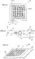
- an LED lamp with a bullet-shaped appearance as disclosed in Japanese Patent No. 2998696may have a configuration such as that illustrated in FIG. 1 , for example.
- the LED lamp 200includes an LED chip 121 , a bullet-shaped transparent housing 127 to cover the LED chip 121 , and leads 122 a and 122 b to supply current to the LED chip 121 .
- a cup reflector 123 for reflecting the emission of the LED chip 121 in the direction indicated by the arrow Dis provided for the mount portion of the lead 122 b on which the LED chip 121 is mounted.
- the LED chip 121 on the mount portionis encapsulated with a first resin portion 124 , in which a phosphor 126 is dispersed and which is further encapsulated with a second resin portion 125 . If the LED chip 121 emits a blue light ray, the phosphor 126 converts a portion of the blue light ray into a yellow light ray. As a result, the blue and yellow light rays are mixed together to produce white light.
- an LED lamppreferably includes a plurality of LEDs that are arranged as an array. LED lamps of that type are disclosed in Japanese Patent Application Laid-Open Publications No. 2003-59332 and No. 2003-124528. A relevant prior art is also disclosed in Japanese Patent Application Laid-Open Publication No. 2004-172586.
- Japanese Patent Application Laid-Open Publication No. 2004-172586discloses an LED lamp that can overcome the color unevenness problem of the bullet-type LED lamp disclosed in Japanese Patent No. 2998696.
- the first resin portion 124is formed by filling the cup reflector 123 with a resin to encapsulate the LED chip 121 and then curing the resin. For that reason, the first resin portion 124 easily has a rugged upper surface as shown in FIG. 2 .
- the thickness of the resin including the phosphor 126loses its uniformity, thus making non-uniform the amounts of the phosphor 126 present along the optical paths E and F of multiple light rays going out of the LED chip 121 through the first resin portion 124 . As a result, the unwanted color unevenness is produced.
- FIGS. 3A and 3Bare respectively a side cross-sectional view and a plan view illustrating an LED lamp as disclosed in Japanese Patent Application Laid-Open Publication No. 2004-172586.
- an LED (LED bare chip) 112 mounted on a substrate 111is covered with a resin portion 113 in which a phosphor is dispersed.
- a reflector 151 with a reflective surface 151 ais bonded to the substrate 111 such that the reflective surface 151 a of the reflector 151 is spaced apart from the side surface of the resin portion 113 .
- the shape of the resin portion 113can be freely designed without being restricted by the shape of the reflective surface 151 a of the reflector 151 .
- the color unevennesscan be reduced significantly.
- an LED arraysuch as that shown in FIG. 4 is obtained.
- the resin portions 113each covering its associated LED chip 112 , are arranged in matrix on the substrate 111 , and a reflector 151 , having a plurality of reflective surfaces 151 a for the respective resin portions 113 , is bonded onto the substrate 111 .
- the luminous fluxes of a plurality of LEDscan be combined together.
- a luminous fluxcomparable to that of an incandescent lamp, a fluorescent lamp or any other general illumination source that is used extensively today, can be obtained easily.
- the LED lamp 300 shown in FIG. 4is used as general illumination, no color unevenness will be produced and a sufficiently high luminous flux can be obtained.
- the present inventorsfurther analyzed this LED lamp 300 to discover that the LED lamp 300 with such a high luminous flux (which is sometimes called a “high-flux LED lamp”) often produces an uncomfortable glaring impression on the viewer although everybody in the prior art has been paying most of their attention to how to increase the luminous flux of the LED lamp. That is to say, as for general illumination, “the brighter, the better” policy is often too simple to work and it is not preferable to make such a glaring impression on the viewer.
- the “glare”refers to viewer's uncomfortableness or decreased ability to recognize small objects, or even every object in general, due to an inadequate luminance distribution within his or her vision, which is formed by the excessively high luminance of the luminaire within his or her sight.
- the viewertends to find a light source very glaring (i) if the luminance of the light source exceeds a certain limit, (ii) if the viewer's eyes have got used to the darkness surrounding him or her, (iii) if the source of the glare is too close to his or her eyes, and/or (iv) if the apparent size or the number of the glaring sources is big.
- the vieweris very likely to find an LED lamp glaring if the LED lamp includes a plurality of LEDs, has a high luminance, and is used in a relatively dark place.
- the LED lampuses the emissions of multiple LEDs and therefore has a much stronger directivity than that of a fluorescent lamp, for example.
- the LED lamptends to produce a stronger glaring impression on the viewer in many cases.
- the luminance of the LED lampwere decreased to reduce such a glare, then the LED lamp would be too dark to use as general illumination.
- preferred embodiments of the present inventionprovide an LED lamp that can reduce the glare significantly.
- An LED lamppreferably includes: a substrate; a cluster of LEDs, which are arranged two-dimensionally on the substrate; and an interconnection circuit, which is electrically connected to the LEDs.
- the LEDspreferably include a first group of LEDs, which are located around the outer periphery of the cluster, and a second group of LEDs, which are located elsewhere in the cluster.
- the interconnection circuitpreferably has an interconnection structure for separately supplying drive currents to at least one of the LEDs in the first group and to at least one of the LEDs in the second group separately from each other.
- the interconnection circuitpreferably has a first interconnection pattern for electrically connecting together at least two of the LEDs in the first group and a second interconnection pattern for electrically connecting together at least two of the LEDs in the second group.
- the interconnection circuitis preferably electrically connected to a dimmer.
- the dimmerpreferably has the function of controlling the amounts of light emitted from the first and second groups of LEDs, which are electrically connected to the first and second interconnection patterns, respectively, independently of each other.
- the first interconnection pattern of the interconnection circuitis preferably electrically connected to a dimmer.
- the dimmerpreferably has the function of controlling the amount of light emitted from the first group of LEDs, which are electrically connected to the first interconnection pattern.
- the LED lamppreferably further includes a resistor, which is connected to at least one of the first and second interconnection patterns.
- the resistorpreferably reduces a difference between the amounts of currents flowing through the first and second interconnection patterns.
- each said LEDpreferably includes an LED bare chip and a phosphor resin portion that covers the LED bare chip.
- the phosphor resin portionpreferably includes: a phosphor for transforming the emission of the LED bare chip into light having a longer wavelength than the emission; and a resin in which the phosphor is dispersed.
- the outer peripheryis preferably defined along the outermost ones of the LEDs in the first group.
- each said LEDpreferably includes a lens for controlling the spatial distribution of the emission of the LED, and the lens of the LEDs in the second group preferably has a structure that realizes a narrower spatial distribution than the lens of the LEDs in the first group.
- the emission of the LEDs in the first grouppreferably has a lower color temperature than that of the LEDs in the second group.
- An LED lamp according to any of various preferred embodiments of the present invention described abovecan control the amount of light emitted from LEDs located around the outer periphery and the amount of light emitted from LEDs located elsewhere independently of each other.
- the luminance of the outer LEDswhich changes the degree of glare significantly, can be controlled selectively. As a result, the glare can be reduced effectively.
- FIG. 1is a cross-sectional view schematically illustrating a configuration for an LED lamp with a bullet shaped appearance as disclosed in Japanese Patent No. 2998696.
- FIG. 2is an enlarged cross-sectional view illustrating a main portion of the LED lamp shown in FIG. 1 .
- FIGS. 3A and 3Bare respectively a side cross-sectional view and a plan view illustrating an LED lamp as disclosed in Japanese Patent Application Laid-Open Publication No. 2004-172586.
- FIG. 4is a perspective view illustrating an exemplary configuration in which the LED lamps shown in FIGS. 3A and 3B are arranged in matrix.
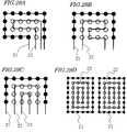
- FIG. 5is a plan view illustrating an LED lamp 400 in which four LEDs 10 are arranged.
- FIG. 6Ashows a circuit 410 in which the four LEDs 10 are connected in series together
- FIG. 6Bshows a circuit 420 in which the four LEDs 10 are connected in parallel to each other.
- FIG. 7is a circuit diagram showing a circuit 430 obtained by connecting four serial connections of the LEDs 10 parallel to each other.
- FIG. 8is a circuit diagram showing a circuit 440 obtained by connecting four parallel connections of the LEDs 10 in series to each other.
- FIG. 9is a perspective view schematically illustrating a state where an LED lamp 500 , including 16 LEDs 10 arranged as a 4 ⁇ 4 matrix, is turned ON.
- FIG. 10is a perspective view schematically illustrating an arrangement for an LED lamp 100 according to a first specific preferred embodiment of the present invention.
- FIG. 11is a cross-sectional view schematically illustrating a configuration for an LED 10 .
- FIG. 12is a circuit diagram showing a configuration for an LED lamp 100 according to the first preferred embodiment of the present invention.
- FIG. 13is a circuit diagram showing a configuration for another LED lamp 100 according to the first preferred embodiment of the present invention.
- FIG. 14is a circuit diagram showing a configuration for a dimmer 30 .
- FIG. 15is a perspective view schematically illustrating a configuration for a card LED lamp 100 according to the first preferred embodiment of the present invention.
- FIG. 16is a perspective view illustrating how the card LED lamp 100 may be used.
- FIG. 17is a cross-sectional view illustrating an LED 10 and its surrounding portions in an LED lamp 100 including a reflector 151 .
- FIG. 18is a perspective view schematically illustrating a configuration for a desk lamp 150 .
- FIG. 19is a perspective view schematically illustrating a configuration for another desk lamp 150 .
- FIG. 20is a perspective view schematically illustrating a configuration for still another desk lamp 150 .
- FIG. 21is a perspective view schematically illustrating a configuration for a flashlight 160 .
- FIGS. 22A and 22Bare enlarged cross-sectional views illustrating two main portions of an LED lamp according to a second specific preferred embodiment of the present invention.
- FIG. 23is a perspective view showing the process step of forming multiple phosphor resin portions 13 by a screen process printing technique.
- FIG. 24is a perspective view showing the process step of forming multiple phosphor resin portions 13 by an intaglio printing technique.
- FIGS. 25A and 25Bare plan views showing the upper and lower surfaces 52 a and 52 b of the block 52 for use in the intaglio printing process.
- FIG. 26is a perspective view showing the process step of forming multiple phosphor resin portions 13 by a transfer (planographic) technique.
- FIG. 27is a perspective view showing the process step of forming multiple phosphor resin portions 13 by a dispenser method.
- FIGS. 28A and 28Bare respectively a side cross-sectional view and a plan view illustrating a configuration in which two LED bare chips 12 A and 12 B are arranged within a single phosphor resin portion 13 .
- FIGS. 29A through 29Dillustrate exemplary interconnection structures for LED lamps according to alternative preferred embodiments of the present invention.
- FIG. 5illustrates an LED lamp 400 in which four LEDs 10 are arranged on a substrate 11 .
- the LED lamp 400 shown in FIG. 5if the four LEDs 10 thereof are connected in series to each other, then the circuit 410 shown in FIG. 6A is obtained.
- the circuit 420 shown in FIG. 6Bis obtained.
- the serial and parallel connectionsmay be combined together.
- the circuit 430 shown in FIG. 7may be obtained by connecting together four serial connections of LEDs 10 parallel to each other.
- the circuit 440 shown in FIG. 8may also be obtained by connecting together four parallel connections of LEDs 10 in series to each other.
- the multiple LEDs 10emit light rays with the same luminous flux. However, even if those LEDs 10 emit the light rays with the same luminous flux, not all of those light rays are directed toward the same object (e.g., a book in a situation where the LED lamp is used as a desk lamp). That is to say, since the light rays diffuse, some of the light rays are directed toward the particular object but others diffuse toward the surroundings.
- FIG. 9schematically illustrates a lighted state of an LED lamp 500 in which sixteen LEDs 10 are arranged as a 4 ⁇ 4 array on a substrate 11 .
- these LEDs 10may be connected together so as to form either the circuit 430 shown in FIG. 7 or the circuit 440 shown in FIG. 8 .
- the light rays Awhich have been radiated from outer LEDs 10 a among the sixteen LEDs 10 arranged as the 4 ⁇ 4 matrix, tend to diffuse more easily than the light rays B that have been radiated from the other inner LEDs 10 b .
- the light rays Btend to be directed toward the object such as a book easily and can perform the function of illuminating the object fully.
- the light rays Amight reach the eyes of the viewer who does not like the light's striking his or her eyes. Accordingly, the light rays A, radiated from the outer LEDs 10 a , are likely to leave the unwanted glaring impression on the viewer.
- the LED lamp 500 shown in FIG. 9To prevent the LED lamp 500 shown in FIG. 9 from producing the glare, not just the luminous flux of the light rays A but also that of the light rays B need to be reduced as well. This is because the LED lamp 500 adopts a circuit configuration that equalizes the luminous fluxes of the respective LEDs 10 . That is to say, as long as the circuit configuration shown in FIG. 7 or 8 is adopted, it is impossible to selectively decrease the luminous fluxes of the outer LEDs 10 a only. However, if the currents supplied to the respective LEDs 10 were all decreased uniformly, then the overall luminous flux of the light striking the object would be too low to use the LED lamp 500 as general illumination.
- the present inventorsgot the basic idea of the present invention by discovering that the glare should be reduced effectively by providing two separate circuits for the outer LEDs 10 a and the inner LEDs 10 b , respectively, and by selectively adjusting the luminance of the outer LEDs 10 a only.
- FIG. 10schematically shows an arrangement for the LED lamp 100 .
- the LED lamp 100includes a substrate 11 , a plurality of LEDs 10 arranged two-dimensionally on the substrate 11 , and an interconnection circuit 20 that is electrically connected to the LEDs 10 .
- the LEDs 10make up a cluster of LEDs that are densely arranged two-dimensionally.
- the LEDs 10 included in that LED clusterare roughly classified into the two groups. Specifically, a first group consists of the LEDs 10 a that are located in the outside portion of the cluster, while a second group consists of the LEDs 10 b that are located in the inside portion of the cluster.
- the interconnection circuit 20 of this preferred embodimentincludes a first interconnection pattern 21 and a second interconnection pattern 22 , which is provided independently of the first interconnection pattern 21 .
- the first and second interconnection patterns 21 and 22are provided for the first and second groups of LEDs, respectively. That is to say, the outer LEDs 10 a are electrically connected to the first interconnection pattern 21 , while the inner LEDs 10 b are electrically connected to the second interconnection pattern 22 .
- the LEDs 10 a located around the outer periphery and the LEDs 10 b located elsewhereare connected to mutually different interconnection patterns 21 and 22 , respectively, and therefore, the luminance of the outer LEDs 10 a can be changed selectively. As a result, the glare can be cut down effectively.
- the interconnection circuit 20is electrically connected to a dimmer (not shown) so as to make the dimmer control the amount of the light emitted from the outer LEDs 10 a , which are electrically connected to the first interconnection pattern 21 , and the amount of the light emitted from the inner LEDs 10 b , which are electrically connected to the second interconnection pattern 22 , independently of each other, then no glare should be produced.
- the first interconnection pattern 21may be electrically connected to the dimmer (not shown) so as to control the amount of light emitted from the outer LEDs 10 a.
- FIG. 11schematically illustrates the cross-sectional structure of an LED 10 according to this preferred embodiment.
- the LED 10includes an LED bare chip 12 and a phosphor resin portion 13 that covers the LED bare chip 12 .
- the phosphor resin portion 13includes a phosphor (or luminophor) for transforming the emission of the LED bare chip 12 into light having a longer wavelength than the emission and a resin in which the phosphor is dispersed.
- the LED bare chip 12is mounted on the substrate 11 , on which the first and second interconnection patterns 21 and 22 shown in FIG. 10 are provided.
- the LED bare chip 12is an LED chip that produces light having a peak wavelength falling within the visible range of 380 nm to 780 nm.
- the phosphor dispersed in the phosphor resin portion 13produces an emission that has a different peak wavelength from that of the LED bare chip 12 within the visible range of 380 nm to 780 nm.
- the LED bare chip 12is a blue LED that emits a blue light ray and the phosphor included in the phosphor resin portion 13 is a yellow phosphor that transforms the blue ray into a yellow ray. The blue and yellow rays are mixed together to produce white light.
- the LED bare chip 12is preferably an LED chip made of a gallium nitride (GaN) based material and emits light with a wavelength of 460 nm, for example.
- GaNgallium nitride
- the phosphor resin portion 13preferably has a substantially cylindrical shape. If the LED bare chip 12 has approximately 0.3 mm ⁇ 0.3 mm dimensions, then the phosphor resin portion 13 may have a diameter of about 0.7 mm to about 0.9 mm, for example.
- the LEDs 10are arranged in a 4 ⁇ 4 matrix on the substrate 11 .
- the number of the LEDs 10does not have to be sixteen as shown in FIG. 10 but may be the product of N and M (where N and M are both integers that are equal to or greater than two).
- the two-dimensional arrangement of the LEDs 10is not limited to the matrix arrangement such as that shown in FIG. 10 , either, but may also be a substantially concentric arrangement, a spiral arrangement or any other suitable arrangement. In any of those alternative arrangements, at least the amount of the light emitted from the outer LEDs 10 a , which is a primary cause of the glare, has to be controlled by connecting the LEDs 10 a to the interconnection pattern 21 .
- FIG. 12shows a circuit configuration for an LED lamp 100 in which sixty-four LEDs 10 are arranged as an 8 ⁇ 8 matrix.
- the LEDs 10 a located around the outer peripheryare connected to a first interconnection pattern 21
- the other LEDs 10 b located elsewhereare connected to a second interconnection pattern 22 .
- the number of the outer LEDs 10 ais different from that of the inner LEDs 10 b , and therefore, a resistor 23 is additionally provided for the second interconnection pattern 22 in order to substantially equalize the amounts of currents flowing through the first and second interconnection patterns 21 and 22 with each other.
- the number of the outer LEDs 10 amay be equalized with that of the inner LEDs 10 b as shown in FIG. 13 .
- the amounts of currents flowing through the first and second interconnection patterns 21 and 22are typically equal to each other, and there is almost no need to provide the resistor 23 such as that shown in FIG. 12 .
- FIG. 14shows an exemplary dimmer 30 to be electrically connected to the first interconnection pattern 21 .
- the dimmer 30 shown in FIG. 14has its circuit configuration designed such that an AC voltage supplied from an AC outlet 31 (e.g., an AC voltage of 100 V) is rectified and converted into a DC voltage and then the power is controlled with a regulator 36 .
- the dimmer 30includes a fuse 32 , a power transformer 33 , a diode bridge 34 , a smoothing capacitor 35 and the regulator 36 .
- the terminal 37outputs a DC voltage (positive) and the terminal 38 has a ground potential.
- the terminals 37 and 38are preferably connected to the first interconnection pattern 21 .
- the positive and negative terminals of the first interconnection pattern 21 shown in FIG. 12 or 13may be respectively connected to the terminals 37 and 38 of the dimmer 30 .
- the regulator 36preferably controls the amount of the current to be supplied to the outer LEDs 10 a, which are connected to the first interconnection pattern 21 , thereby controlling the amount of the light emitted from those outer LEDs 10 a.
- two dimmers 20may be provided and connected to the first and second interconnection patterns 21 and 22 , respectively.
- the amounts of light emitted from the two groups of LEDs 10 a and 10 bcan be controlled independently of each other.
- the dimmer(s) for controlling the amount(s) of light emitted from the LEDs 10 a (and 10 b )does not have to have the configuration shown in FIG. 14 but may have any other suitable configuration.
- the LED lamp 100 of this preferred embodimentis making a glaring impression on the viewer, that glare can be erased quickly by getting the amount of the light emitted from the outer LEDs 10 a controlled by the dimmer 30 . In that case, the amount of the light emitted from the inner LEDs 10 b can be kept as it is. Thus, the glare can be reduced without decreasing the overall luminous flux of the LED lamp 100 .
- the light emitted from the inner LEDs 10 billuminates the object exclusively.
- the “object”may refer to a book, for example, when the LED lamp 100 is used as a desk or bedside lamp. Accordingly, even if the luminous flux of the LED lamp 100 decreased significantly, there might still be no problem as long as the user can view the object (e.g., read that book) satisfactorily.
- a lens structure that realizes a sufficiently narrow spatial distribution of emissionis provided in front of the inner LEDs 10 b , most of the light illuminating the object comes from the inner LEDs 10 b . Accordingly, the amount of the light illuminating the object can be kept substantially constant even when the amount of light coming from the outer LEDs 10 a is controlled.
- a switching mechanism for selectively turning the LEDs 10 a ON and OFFmay also be adopted. Then, the object can be illuminated with the light cast from the LEDs 10 b with the glare reduced by turning the LEDs 10 a OFF.
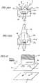
- the LED lamp 100 of this preferred embodimentmay also be implemented as a card LED lamp such as that shown in FIG. 15 .
- the substrate 11includes a feeder section 120 , which is electrically connected to the LEDs 10 by way of the first and second interconnection patterns 21 and 22 embedded in the substrate 11 .
- the detailed configuration of the feeder section 120is not shown in FIG. 15 .
- a feeder terminalmay be provided on the surface of the feeder section 120 .
- the substrate 11 and the reflector ( 151 )may be collectively called the “substrate” of the LED lamp 100 .
- the substrate 11itself may be used as an optical reflective member.
- FIG. 16shows the LED lamp 100 obtained by bonding the reflector 151 to the substrate 11 , a connector 130 to/from which the LED lamp 100 is attachable and removable freely, and a lighting circuit 133 to be electrically connected to the LED lamp 100 by way of the connector 130 .
- the lighting circuit 133preferably has the function of controlling either the amount of the light emitted from the outer LEDs 10 a only or the amounts of the light emitted from the outer and inner LEDs 10 a and 10 b independently of (or in cooperation with) each other.
- the LED lamp 100is inserted into the connector 130 that has a pair of guide grooves 131 .
- the connector 130includes a feeder electrode (not shown) to be electrically connected to the feeder electrode (not shown, either) that is provided on the feeder section 120 of the LED lamp 100 .
- the feeder electrode of the connector 130is electrically connected to the lighting circuit 133 by way of lines 132 .
- FIG. 17is a cross-sectional view illustrating a portion of the LED lamp 100 with the reflector 151 , surrounding the LED 10 , on a larger scale.
- the LED bare chip 12is flip-chip bonded to an interconnection pattern 42 of a multilayer wiring board 41 , which is attached to the metal plate 40 .
- the metal plate 40 and the multilayer wiring board 41together make up the substrate 11 .
- the LED bare chip 12is covered with the phosphor resin portion 13 .
- the phosphor resin portion 13is further covered with a lens 14 , which may be made of a resin, for example.
- the multilayer wiring board 41includes a two-layered interconnection pattern 42 , in which interconnects belonging to the two different layers are connected together by way of via metals 43 .
- the interconnects 42 belonging to the upper layerare connected to the electrodes of the LED chip 12 via Au bumps 44 .
- an underfill (stress relaxing) layer 45is preferably provided between the reflector 151 and the multilayer wiring board 41 .
- This underfill layer 45can not only relax the stress, resulting from the difference in thermal expansion coefficient between the metallic reflector 151 and the multilayer wiring board 42 , but also ensure electrical insulation between the reflector 151 and the upper-level interconnects of the multilayer wiring board 41 .
- the reflector 151has an opening 15 to accommodate the phosphor resin portion 13 that covers the LED bare chip 12 .
- the side surface defining the opening 15is used as a reflective surface 151 a for reflecting the light that has been emitted from the LED 10 .
- the reflective surface 151 ais spaced apart from the side surface of the phosphor resin portion 13 such that the shape of the phosphor resin portion 13 is not affected by the reflective surface 151 a so much as to produce color unevenness.
- the specifics and effects of this spacing arrangementare described in Japanese Patent Application Laid-Open Publication No. 2004-172586, the entire contents of which are hereby incorporated by reference.
- FIGS. 10 and 15show substantially cylindrical phosphor resin portions 13 .
- the “substantially cylindrical” shapemay refer to not only a completely circular cross section but also a polygonal cross section with at least six vertices. This is because a polygon with at least six vertices substantially has axial symmetry and can be virtually identified with a “circle”.
- a phosphor resin portion 13 with such a substantially cylindrical shapeeven if the LED bare chip 12 being ultrasonic flip-chip bonded to the substrate 11 rotated due to the ultrasonic vibrations applied thereto, the luminous intensity distribution of the LED would not be affected so easily.
- the LED lamp 100 of this preferred embodimentis easily applicable to a desk or bedside lamp or to a flashlight.
- FIGS. 18 , 19 and 20show exemplary applications of the card LED lamp 100 to desk lamps 150 .
- FIG. 21shows an exemplary application of the card LED lamp 100 to a flashlight 160 .
- the desk lamp 150 shown in FIG. 18is designed so as to illuminate the object by using just one card LED lamp 100 .
- the amount of the light emitted from the outer LEDs 10 acan be controlled as described above.
- the base 135 of the desk lamp 150includes a controller dial (anti-glare dial) 136 such that the glare can be cut down by adjusting the dial 136 .
- FIG. 19schematically illustrates a configuration for a desk lamp 150 that uses two card LED lamps 100 at the same time.
- the desk lamps shown in FIGS. 18 and 19use the card LED lamps 100 .
- the LED lamps 100do not have to be the card type. Even if the desk lamps are operated using non-removable LED lamps 100 , the glare can still be reduced effectively.
- FIG. 20shows a configuration for a desk lamp 150 that uses four LED lamps 100 at the same time.
- some of the LEDs 10 awhich are located around the outer periphery in each LED lamp 100 , become inner LEDs 10 b .
- the LEDs 10 located within the area 155may be used as additional inner LEDs.
- the LEDs 10 located within this area 155may be designed just like the inner LEDs 10 b .
- to mass-produce and use the LED lamps 100 of the same type in quantitieseven the LEDs 10 within the area 155 may be used as outer LEDs 10 a as they are.
- the anti-glare effectsare also achieved no matter whether the card LED lamps 100 are used or not. That is to say, it does not matter whether the LED lamps 100 are removable or not.
- FIG. 21shows a configuration for a flashlight 160 that uses the LED lamp 100 .
- the flashlight 160 shown in FIG. 21includes not only a normal switch 162 for turning this flashlight ON or OFF but also an anti-glare switch 164 as well. Specifically, when the anti-glare switch 164 is pressed down, the light emitted from the outer LEDs 10 a is either decreased or put out, thereby preventing the flashlight 160 from producing the glaring impression.
- the flashlight 160may be used in a normal mode to illuminate a broad range but is preferably switched into the anti-glare mode in order to prevent this flashlight 160 from leaving the glaring impression on the people surrounding it.
- the amount of the light emitted from the outer LEDs 10 awhich changes the degree of the glare, can be controlled selectively among the two-dimensional arrangement of LEDs 10 , and therefore, the glare can be reduced effectively.
- the present inventioncontributes to further popularizing LED lamps as general illumination units.
- the outer LEDs 10 aare supposed to be outermost ones as shown in FIGS. 10 and 12 . However, as shown in FIG. 13 , even non-outermost LEDs 10 may also be used as the outer LEDs 10 a , too.
- the outermost and second outermost LEDs 10may be used as the outer LEDs 10 a in the arrangement shown in FIG. 12 , for example.
- the white LED lamp 100including a plurality of LEDs 10 each made up of a blue LED chip 12 and a yellow phosphor, has been described.
- a white LED lampwhich produces white light by combining an ultraviolet LED chip, emitting an ultraviolet ray, with a phosphor that produces red (R), green (G) and blue (B) rays when excited with the ultraviolet ray, was also developed recently.
- the LED lamp 100may also be of that type.
- the ultraviolet LED chipemits an ultraviolet ray with a peak wavelength of 200 nm to 410 nm.
- the phosphor producing red (R), green (G) and blue (B) rayshas peak wavelengths of 450 nm, 540 nm and 610 nm within the visible range of 380 nm to 780 nm.
- the LED 10is supposed to include the LED bare chip 12 .
- the LEDdoes not always have to include a LED bare chip.
- the same anti-glare effectsare achievable by applying the present invention to any other type of LED lamp as long as the outer LEDs of the LED lamp might produce the glaring impression.
- the anti-glare effectsare also achievable in not just the white LED lamp of the preferred embodiment described above but also a single-color LED lamp emitting an R, G or B ray.
- the LED lamp (or LED module)includes at least four LEDs 10
- the LEDs 10can be grouped into the outer LEDs 10 a and inner LEDs 10 b.
- the amount of the light emitted from the outer LEDs 10 ais controlled appropriately, thereby reducing the glare effectively.
- an arrangement for further reducing the glareis adopted.
- FIGS. 22A and 22Bschematically illustrate a configuration for a lens 14 a that covers the outer LED 10 a and a configuration for a lens 14 b that covers the inner LED 10 b , respectively.
- the inner lens 14 bhas a lens structure that forms a narrower luminous intensity distribution than the outer lens 14 a does.
- the inner lenses 14 bmay have a hemispherical convex shape and a half beam angle of 35 degrees or less, for example.
- a color with a relatively low color temperaturee.g., a bulb color
- a relatively high color temperaturee.g., a substantially daylight color including a daylight color and neutral white
- one of the following techniquesmay be adopted.
- One techniqueis to set the volume of the outer phosphor resin portion 13 greater than that of the inner phosphor resin portion 13 . Then, the light emitted from the LED bare chip 12 in the outer LED 10 a has to go through a greater amount of phosphor. Accordingly, the outgoing light of the outer LED 10 a becomes closer to bulb color and comes to have a lower color temperature.
- Another techniqueis to set the concentration of the phosphor in the outer phosphor resin portion 13 higher than that of the phosphor in the inner phosphor resin portion 13 . Then, the light emitted from the LED bare chip 12 in the outer LED 10 a has to go through a greater amount of phosphor. Accordingly, the outgoing light of the outer LED 10 a also becomes closer to bulb color and comes to have a lower color temperature, too.
- the color temperatures of the outgoing light of the inner and outer LEDsmay also be adjusted by changing the types or the mixture ratio of the phosphors for the inner and outer phosphor resin portions 13 .
- the LED lamp 100In fabricating the LED lamp 100 such as that shown in FIG. 15 , it is convenient to adopt a method of forming the multiple phosphor resin portions 13 in the same process step (i.e., at the same time).
- Various methodsmay be used to form the phosphor resin portions 13 simultaneously. Examples of those methods include a screen process printing method, an intaglio printing method, a transfer method and a dispenser method.
- FIG. 23shows the process step of forming the phosphor resin portions 13 by the screen process printing technique.
- a substrate 11 on which multiple LED chips 12 are arrangedis prepared.
- FIG. 23shows only two LED chips 12 to make this method easily understandable. Actually, however, a substrate 11 on which a number of LED chips 12 are arranged two-dimensionally (e.g., in matrix, substantially concentrically or spirally) should be prepared to fabricate the LED lamp 100 of this preferred embodiment.
- a printing plate 51having a plurality of openings (or through holes) 51 a in the same size as that of the phosphor resin portions 13 ( 13 a and 13 b ) to be obtained, is placed over the substrate 11 such that the LED chips 12 are located within the openings 51 a . Then, the printing plate 51 and the substrate 11 are brought into close contact with each other. Thereafter, a squeeze 50 is moved in a printing direction, thereby filling the openings 51 a with a resin paste 60 on the printing plate 51 and covering the LED chips 12 with the resin paste 60 . When the printing process is finished, the printing plate 51 is removed. The phosphor is dispersed in the resin paste 60 .
- the phosphor resin portions 13can be obtained. If the volume of the outer phosphor resin portions 13 should be greater than that of the inner phosphor resin portions 13 , then the openings 51 a for the outer LED chips 12 preferably have an increased size. As for the other methods to be described below, the same process step as this process step of the screen process printing method will not be described again but the description will be focused on only their unique process steps.
- FIG. 24shows the process step of forming the phosphor resin portions 13 by the intaglio printing method.
- FIGS. 25A and 25Brespectively show the upper surface 52 a and lower surface 52 b of a printing plate 52 for use in this intaglio printing process.
- the printing plate 52 shown in FIGS. 25A and 25Bhaving recesses 53 (i.e., not reaching the upper surface 52 a ) on the lower surface 52 b , is prepared and those recesses 53 are filled with a resin paste 60 .
- the printing plate 52is placed over the substrate 11 on which the LED chips 12 are arranged and the printing plate 52 and the substrate 11 are brought into close contact with each other.
- the phosphor resin portions 13can be obtained. If the volume of the outer phosphor resin portions 13 should be greater than that of the inner phosphor resin portions 13 , then the recesses 53 for the outer LED chips 12 preferably have an increased size. That is to say, the recesses 53 may be classified into a group with a relatively large volume and a group with a relatively small volume.
- FIG. 26shows the process step of forming the phosphor resin portions 13 by the transfer (planographic) method.
- a photosensitive resin film 56is deposited on a block 55 , a plurality of openings 57 , corresponding in shape to the phosphor resin portions 13 to be obtained, are provided using a resist, and then those openings 57 are filled with a resin paste 60 .
- the block 55is pressed against the substrate 11 , thereby transferring the resin paste 60 onto the substrate 11 .
- the phosphor resin portions 13are formed so as to cover the LED chips 12 .
- the openings 57 for the outer LED chips 12preferably have an increased size. Also, if the concentration of the phosphor in the outer phosphor resin portions 13 should be higher than that of the phosphor in the inner phosphor resin portions 13 , then a resin paste 60 with a relatively high phosphor concentration may be injected into the openings 57 for the outer LED chips 12 .
- FIG. 27shows the process step of forming the phosphor resin portions 13 by the dispenser method.
- the phosphor resin portions 13are formed by spraying a predetermined amount of resin paste 60 over the LED chips 12 on the substrate 11 using a dispenser 58 including syringes 59 to spray the resin paste 60 . If a greater amount of resin paste 60 is sprayed for the outer phosphor resin portions 13 b than for the inner phosphor resin portions 13 a , then the size, volume and the phosphor concentration of the outer phosphor resin portions 13 b can be all increased.
- the configuration of the phosphor resin portions 13 described above and the lens structures shown in FIGS. 22A and 22Bmay be used in combination. It depends on the specific intended application whether those configurations are combined or not and exactly what configurations should be combined together.
- one LED bare chip 12is provided within one phosphor resin portion 13 .
- the present inventionis in no way limited to those specific preferred embodiments. If necessary, two or more LED bare chips 12 may be provided within a single phosphor resin portion 13 .
- FIGS. 28A and 28Billustrate such an alternative arrangement in which two LED bare chips 12 A and 12 B are provided within one phosphor resin portion 13 .
- the LED bare chips 12 A and 12 Bmay emit either light rays falling within the same wavelength range or light rays falling within mutually different wavelength ranges.
- the LED bare chip 12 Amay be a blue LED chip and the LED bare chip 12 B may be a red LED chip.
- the two or more LED bare chips 12(e.g., 12 A and 12 B in this example) that are covered with the same phosphor resin portion 13 have a peak wavelength of 380 nm to 470 nm (e.g., a wavelength of 460 nm if there is provided only one LED bare chip 12 A of one type) and a peak wavelength of 610 nm to 650 nm (e.g., a wavelength of 620 nm if there is provided only one LED bare chip 12 B of another type). That is to say, the peak wavelengths of the at least two LED bare chips 12 all fall within the visible range of 380 nm to 780 nm.
- a white LED lampof which the color rendering performance is excellent in red colors, can be obtained. More specifically, if a blue LED chip and a yellow phosphor are combined, white can be produced but that white is somewhat short of red components. Consequently, the resultant white LED lamp exhibits insufficient color rendering performance in red colors. However, if the red LED chip 12 B is combined with the blue LED chip 12 A, then the color rendering performance of the white LED lamp in red colors can be improved. As a result, an LED lamp that can be used even more effectively as general illumination is realized.
- the present inventionhas been described by way of illustrative preferred embodiments. However, the present invention is in no way limited to those specific preferred embodiments but may be modified in various manners. For example, in the configurations shown in FIGS. 12 and 13 , the LEDs 10 may also be connected in parallel to each other.
- first interconnection pattern for electrically connecting together the LEDs 10 located around the outer periphery and the second interconnection pattern for electrically connecting together the other LEDs 10 located elsewhereare not limited to those shown in FIGS. 12 and 13 . Hereinafter, this respect will be described in detail.
- FIGS. 29A through 29Dillustrate alternative interconnection structures for LED lamps according to other preferred embodiments of the present invention.
- the solid circles ⁇represent LEDs to be connected to one interconnection pattern and the open circles ⁇ represent LEDs to be connected to another interconnection pattern.
- FIG. 29Cshows a situation where the interconnection structure has three interconnection patterns 21 , 22 and 23 .
- the number of the interconnection patterns that a single LED lamp hasis not always two but may be three or more.
- two clusters of LEDsare arranged within a single LED lamp.
- the LEDs located in the outside portion of each LED clusterare connected to the first interconnection pattern 21
- the LEDs located in the inside portion thereofare connected to the second interconnection pattern 22 . If these two LED clusters are provided sufficiently close to each other, these two clusters function as one cluster of LEDs. However, if the gap between these two LED clusters exceeds 4 mm, for example, the interconnection structure, which can control the amount of the light emitted from the outer LEDs of each cluster, may be adopted as shown in FIG. 29D .
- the first interconnection pattern 21 for the LED cluster on the left-hand side and the first interconnection pattern 21 for the LED cluster on the right-hand sideare preferably connected together by way of a lower-level interconnect (not shown).
- the second interconnection pattern 22 for the LED cluster on the left-hand side and the second interconnection pattern 22 for the LED cluster on the right-hand sideare preferably connected together by way of another lower-level interconnect (not shown). Accordingly, the amounts of light emitted from the LEDs in the right and left LED clusters can be controlled in the same way. Alternatively, if a number of LED clusters are included in a single LED lamp, the amounts of light emitted from the LEDs in those clusters may also be controlled independently of each other.
- Various preferred embodiments of the present invention described aboveprovide an LED lamp that can reduce the glare significantly, and therefore, contribute to further popularizing LED lamps as general illumination.
Landscapes
- Engineering & Computer Science (AREA)
- General Engineering & Computer Science (AREA)
- Physics & Mathematics (AREA)
- Microelectronics & Electronic Packaging (AREA)
- Optics & Photonics (AREA)
- Led Device Packages (AREA)
- Non-Portable Lighting Devices Or Systems Thereof (AREA)
Abstract
Description
Claims (16)
Applications Claiming Priority (2)
| Application Number | Priority Date | Filing Date | Title |
|---|---|---|---|
| JP2003-322645 | 2003-09-16 | ||
| JP2003322645 | 2003-09-16 |
Publications (2)
| Publication Number | Publication Date |
|---|---|
| US20050057929A1 US20050057929A1 (en) | 2005-03-17 |
| US7204607B2true US7204607B2 (en) | 2007-04-17 |
Family
ID=34270005
Family Applications (1)
| Application Number | Title | Priority Date | Filing Date |
|---|---|---|---|
| US10/940,860Expired - LifetimeUS7204607B2 (en) | 2003-09-16 | 2004-09-14 | LED lamp |
Country Status (1)
| Country | Link |
|---|---|
| US (1) | US7204607B2 (en) |
Cited By (58)
| Publication number | Priority date | Publication date | Assignee | Title |
|---|---|---|---|---|
| US20050264686A1 (en)* | 2004-05-31 | 2005-12-01 | Yoshiharu Tenmyo | Illumination apparatus and image-taking apparatus |
| US20060139245A1 (en)* | 2004-12-27 | 2006-06-29 | Tooru Sugiyama | Projection video display apparatus and brightness adjustment method therefor |
| US20060289880A1 (en)* | 2005-06-28 | 2006-12-28 | Makoto Kurihara | Illuminating device and display device including the same |
| US20070013647A1 (en)* | 2005-07-15 | 2007-01-18 | Samsung Electro-Mechanics Co., Ltd. | Surface light source using LED and backlight unit having the surface light source |
| US20070177378A1 (en)* | 2006-02-01 | 2007-08-02 | Ting-Feng Wu | Full color flashlight with high power LED |
| US20080042555A1 (en)* | 2006-08-15 | 2008-02-21 | Au Optronics Corp. | Backlight source |
| US20080133782A1 (en)* | 2006-12-01 | 2008-06-05 | Lg Electronics Inc. | Reception system and method of processing interface information |
| US20080247162A1 (en)* | 2005-05-25 | 2008-10-09 | Neobulb Technologies, Inc. | Light-Emitting Diode Cluster Lamp |
| US20090050908A1 (en)* | 2005-01-10 | 2009-02-26 | Cree, Inc. | Solid state lighting component |
| US20090141476A1 (en)* | 2005-06-07 | 2009-06-04 | Noam Meir | Illumination Apparatus and Methods of Forming the Same |
| US20090161341A1 (en)* | 2007-12-19 | 2009-06-25 | Noam Meir | Planar White Illumination Apparatus |
| US20090161361A1 (en)* | 2007-12-19 | 2009-06-25 | Noam Meir | Discrete lighting elements and planar assembly thereof |
| US20090225565A1 (en)* | 2008-03-05 | 2009-09-10 | Micha Zimmermann | Sub-assembly and methods for forming the same |
| US20090303694A1 (en)* | 2006-03-31 | 2009-12-10 | Seoul Semiconductor Co., Ltd. | Light emitting device and lighting system having the same |
| US20100002414A1 (en)* | 2005-06-07 | 2010-01-07 | Noam Meir | Illumination Apparatus and Methods of Forming the Same |
| US20100008628A1 (en)* | 2008-07-10 | 2010-01-14 | Yosi Shani | Slim waveguide coupling apparatus and method |
| US20100098377A1 (en)* | 2008-10-16 | 2010-04-22 | Noam Meir | Light confinement using diffusers |
| US20100103660A1 (en)* | 2008-10-24 | 2010-04-29 | Cree Led Lighting Solutions, Inc. | Array layout for color mixing |
| US20100208469A1 (en)* | 2009-02-10 | 2010-08-19 | Yosi Shani | Illumination surfaces with reduced linear artifacts |
| US20100220484A1 (en)* | 2008-07-10 | 2010-09-02 | Oree Inc. | Slim waveguide coupling apparatus and method |
| US20100254129A1 (en)* | 2006-04-18 | 2010-10-07 | Cree, Inc. | Saturated yellow phosphor converted led and blue converted red led |
| US20100301371A1 (en)* | 2004-06-10 | 2010-12-02 | Seoul Semiconductor Co., Ltd. | Light emitting device |
| US20100315817A1 (en)* | 2009-05-13 | 2010-12-16 | Oree Inc. | Low-profile illumination device |
| US20110043137A1 (en)* | 2009-08-19 | 2011-02-24 | Cree Led Lighting Solutions, Inc. | White light color changing solid state lighting and methods |
| US20110148327A1 (en)* | 2009-12-21 | 2011-06-23 | Van De Ven Antony P | High cri adjustable color temperature lighting devices |
| CN102147065A (en)* | 2011-01-13 | 2011-08-10 | 惠州雷士光电科技有限公司 | Combined lighting device |
| US8038321B1 (en) | 2008-05-06 | 2011-10-18 | Koninklijke Philips Electronics N.V. | Color mixing luminaire |
| US8038327B1 (en) | 2008-05-06 | 2011-10-18 | Genlyte Thomas Group Llc | Color mixing luminaire |
| US20110261555A1 (en)* | 2010-04-22 | 2011-10-27 | Franklin Electronic Publishers, Incorporated | Led reading light |
| US8128272B2 (en) | 2005-06-07 | 2012-03-06 | Oree, Inc. | Illumination apparatus |
| EP2236010A4 (en)* | 2008-01-25 | 2012-05-30 | Eveready Battery Inc | LIGHTING DEVICE HAVING FADE AND METHOD THEREOF |
| US8272757B1 (en)* | 2005-06-03 | 2012-09-25 | Ac Led Lighting, L.L.C. | Light emitting diode lamp capable of high AC/DC voltage operation |
| US8431954B2 (en) | 2007-08-28 | 2013-04-30 | Seoul Semiconductor Co., Ltd. | Light emitting device employing non-stoichiometric tetragonal alkaline earth silicate phosphors |
| US8501040B2 (en) | 2007-08-22 | 2013-08-06 | Seoul Semiconductor Co., Ltd. | Non-stoichiometric tetragonal copper alkaline earth silicate phosphors and method of preparing the same |
| US8591072B2 (en) | 2011-11-16 | 2013-11-26 | Oree, Inc. | Illumination apparatus confining light by total internal reflection and methods of forming the same |
| US8624527B1 (en) | 2009-03-27 | 2014-01-07 | Oree, Inc. | Independently controllable illumination device |
| USD700584S1 (en) | 2011-07-06 | 2014-03-04 | Cree, Inc. | LED component |
| US8698171B2 (en) | 2005-01-10 | 2014-04-15 | Cree, Inc. | Solid state lighting component |
| US8727597B2 (en) | 2009-06-24 | 2014-05-20 | Oree, Inc. | Illumination apparatus with high conversion efficiency and methods of forming the same |
| US8810133B2 (en) | 2009-06-30 | 2014-08-19 | Koninklijke Philips N.V. | Grid for illumination apparatus |
| US8883040B2 (en) | 2004-06-10 | 2014-11-11 | Seoul Semiconductor Co., Ltd. | Luminescent material |
| US8900482B2 (en) | 2004-06-10 | 2014-12-02 | Seoul Semiconductor Co., Ltd. | Light emitting device |
| US20160131313A1 (en)* | 2014-11-11 | 2016-05-12 | Toyoda Gosei Co., Ltd. | Light emitting device |
| US9786811B2 (en) | 2011-02-04 | 2017-10-10 | Cree, Inc. | Tilted emission LED array |
| US9857519B2 (en) | 2012-07-03 | 2018-01-02 | Oree Advanced Illumination Solutions Ltd. | Planar remote phosphor illumination apparatus |
| US10295147B2 (en) | 2006-11-09 | 2019-05-21 | Cree, Inc. | LED array and method for fabricating same |
| US10349479B2 (en) | 2011-12-02 | 2019-07-09 | Lynk Labs, Inc. | Color temperature controlled and low THD LED lighting devices and systems and methods of driving the same |
| US10492251B2 (en) | 2004-02-25 | 2019-11-26 | Lynk Labs, Inc. | AC light emitting diode and AC LED drive methods and apparatus |
| US10499466B1 (en) | 2004-02-25 | 2019-12-03 | Lynk Labs, Inc. | AC light emitting diode and AC LED drive methods and apparatus |
| US20190383470A1 (en)* | 2018-06-15 | 2019-12-19 | Arnold & Richter Cine Technik Gmbh & Co. Betriebs Kg | Light-producing assembly for a spotlight and spotlight |
| US10575376B2 (en) | 2004-02-25 | 2020-02-25 | Lynk Labs, Inc. | AC light emitting diode and AC LED drive methods and apparatus |
| US10741107B2 (en) | 2013-12-31 | 2020-08-11 | Ultravision Technologies, Llc | Modular display panel |
| US10842016B2 (en) | 2011-07-06 | 2020-11-17 | Cree, Inc. | Compact optically efficient solid state light source with integrated thermal management |
| US10891881B2 (en) | 2012-07-30 | 2021-01-12 | Ultravision Technologies, Llc | Lighting assembly with LEDs and optical elements |
| US20220066086A1 (en)* | 2017-04-19 | 2022-03-03 | Omachron Intellectual Property Inc. | Led light source |
| US11528792B2 (en) | 2004-02-25 | 2022-12-13 | Lynk Labs, Inc. | High frequency multi-voltage and multi-brightness LED lighting devices |
| US11791442B2 (en) | 2007-10-31 | 2023-10-17 | Creeled, Inc. | Light emitting diode package and method for fabricating same |
| US12279345B2 (en) | 2009-12-28 | 2025-04-15 | Lynk Labs, Inc. | Light emitting diode and LED drive apparatus |
Families Citing this family (16)
| Publication number | Priority date | Publication date | Assignee | Title |
|---|---|---|---|---|
| FR2893811B1 (en)* | 2005-11-21 | 2011-06-03 | Zedel | ELECTRIC LAMP WITH ELECTRICAL ZOOM |
| KR100755612B1 (en)* | 2006-09-21 | 2007-09-06 | 삼성전기주식회사 | Manufacturing method of LED package and manufacturing method of white light source module |
| TWI440210B (en) | 2007-01-22 | 2014-06-01 | Cree Inc | Illumination device using external interconnection array of light-emitting device and manufacturing method thereof |
| US8227999B2 (en)* | 2007-06-04 | 2012-07-24 | Koninklijke Philips Electronics N.V. | Light output device |
| US7905618B2 (en) | 2007-07-19 | 2011-03-15 | Samsung Led Co., Ltd. | Backlight unit |
| EP2131627B1 (en)* | 2008-06-04 | 2013-09-18 | Hochschule für Technik und Wirtschaft Dresden (FH) | Lamp |
| ATE479051T1 (en)* | 2008-06-20 | 2010-09-15 | Trumpf Medizin Systeme Gmbh & Co Kg | OPERATIONAL LIGHT |
| GB2473311B (en)* | 2010-05-21 | 2011-07-27 | Oliver Shakespeare | A lighting device |
| EP2878883A4 (en)* | 2012-07-25 | 2015-11-25 | Panasonic Ip Man Co Ltd | LIGHT EMITTING MODULE |
| JP2014157744A (en)* | 2013-02-15 | 2014-08-28 | Panasonic Corp | Light emitting circuit, light emitting module and lighting apparatus |
| CN103256574B (en)* | 2013-04-18 | 2015-02-04 | 李宪坤 | Intelligent wiring method and system for LED lamps |
| CN104913235A (en)* | 2015-06-25 | 2015-09-16 | 浙江法斯特电梯有限公司 | LED table lamp |
| CN105065993A (en)* | 2015-08-13 | 2015-11-18 | 俞勤 | LED project lamp |
| CN105090805A (en)* | 2015-08-19 | 2015-11-25 | 左颖 | Point control and full color LED luminous characters for wedding celebration decoration |
| JP6655832B2 (en)* | 2016-03-03 | 2020-02-26 | パナソニックIpマネジメント株式会社 | Lighting equipment |
| US20180209614A1 (en)* | 2017-01-20 | 2018-07-26 | Maxim Lighting International, Inc. | Light emitting diode assembly and method of manufacture |
Citations (10)
| Publication number | Priority date | Publication date | Assignee | Title |
|---|---|---|---|---|
| US4963798A (en)* | 1989-02-21 | 1990-10-16 | Mcdermott Kevin | Synthesized lighting device |
| JPH1065221A (en) | 1997-05-17 | 1998-03-06 | Nichia Chem Ind Ltd | Light emitting diode |
| US5865529A (en)* | 1997-03-10 | 1999-02-02 | Yan; Ellis | Light emitting diode lamp having a spherical radiating pattern |
| US5998925A (en) | 1996-07-29 | 1999-12-07 | Nichia Kagaku Kogyo Kabushiki Kaisha | Light emitting device having a nitride compound semiconductor and a phosphor containing a garnet fluorescent material |
| JP2003059332A (en) | 2001-08-17 | 2003-02-28 | Matsushita Electric Works Ltd | Led luminaire |
| US6580228B1 (en)* | 2000-08-22 | 2003-06-17 | Light Sciences Corporation | Flexible substrate mounted solid-state light sources for use in line current lamp sockets |
| US20030189829A1 (en) | 2001-08-09 | 2003-10-09 | Matsushita Electric Industrial Co., Ltd. | LED illumination apparatus and card-type LED illumination source |
| US20040100192A1 (en) | 2002-11-07 | 2004-05-27 | Matsuhita Electric Industrial Co., Ltd. | Led lamp |
| US20040119086A1 (en) | 2002-11-25 | 2004-06-24 | Matsushita Electric Industrial Co. Ltd. | Led Lamp |
| US20040124430A1 (en) | 2002-11-25 | 2004-07-01 | Matsushita Electric Industrial Co., Ltd. | LED lamp |
- 2004
- 2004-09-14USUS10/940,860patent/US7204607B2/ennot_activeExpired - Lifetime
Patent Citations (11)
| Publication number | Priority date | Publication date | Assignee | Title |
|---|---|---|---|---|
| US4963798A (en)* | 1989-02-21 | 1990-10-16 | Mcdermott Kevin | Synthesized lighting device |
| US5998925A (en) | 1996-07-29 | 1999-12-07 | Nichia Kagaku Kogyo Kabushiki Kaisha | Light emitting device having a nitride compound semiconductor and a phosphor containing a garnet fluorescent material |
| US5865529A (en)* | 1997-03-10 | 1999-02-02 | Yan; Ellis | Light emitting diode lamp having a spherical radiating pattern |
| JPH1065221A (en) | 1997-05-17 | 1998-03-06 | Nichia Chem Ind Ltd | Light emitting diode |
| US6580228B1 (en)* | 2000-08-22 | 2003-06-17 | Light Sciences Corporation | Flexible substrate mounted solid-state light sources for use in line current lamp sockets |
| US20030189829A1 (en) | 2001-08-09 | 2003-10-09 | Matsushita Electric Industrial Co., Ltd. | LED illumination apparatus and card-type LED illumination source |
| US6949772B2 (en)* | 2001-08-09 | 2005-09-27 | Matsushita Electric Industrial Co., Ltd. | LED illumination apparatus and card-type LED illumination source |
| JP2003059332A (en) | 2001-08-17 | 2003-02-28 | Matsushita Electric Works Ltd | Led luminaire |
| US20040100192A1 (en) | 2002-11-07 | 2004-05-27 | Matsuhita Electric Industrial Co., Ltd. | Led lamp |
| US20040119086A1 (en) | 2002-11-25 | 2004-06-24 | Matsushita Electric Industrial Co. Ltd. | Led Lamp |
| US20040124430A1 (en) | 2002-11-25 | 2004-07-01 | Matsushita Electric Industrial Co., Ltd. | LED lamp |
Cited By (120)
| Publication number | Priority date | Publication date | Assignee | Title |
|---|---|---|---|---|
| US10506674B2 (en) | 2004-02-25 | 2019-12-10 | Lynk Labs, Inc. | AC light emitting diode and AC LED drive methods and apparatus |
| US10687400B2 (en) | 2004-02-25 | 2020-06-16 | Lynk Labs, Inc. | AC light emitting diode and AC LED drive methods and apparatus |
| US10750583B2 (en) | 2004-02-25 | 2020-08-18 | Lynk Labs, Inc. | AC light emitting diode and AC LED drive methods and apparatus |
| US10966298B2 (en) | 2004-02-25 | 2021-03-30 | Lynk Labs, Inc. | AC light emitting diode and AC LED drive methods and apparatus |
| US11019697B2 (en) | 2004-02-25 | 2021-05-25 | Lynk Labs, Inc. | AC light emitting diode and AC led drive methods and apparatus |
| US10499466B1 (en) | 2004-02-25 | 2019-12-03 | Lynk Labs, Inc. | AC light emitting diode and AC LED drive methods and apparatus |
| US10575376B2 (en) | 2004-02-25 | 2020-02-25 | Lynk Labs, Inc. | AC light emitting diode and AC LED drive methods and apparatus |
| US10492252B2 (en) | 2004-02-25 | 2019-11-26 | Lynk Labs, Inc. | AC light emitting diode and AC LED drive methods and apparatus |
| US11528792B2 (en) | 2004-02-25 | 2022-12-13 | Lynk Labs, Inc. | High frequency multi-voltage and multi-brightness LED lighting devices |
| US11638336B2 (en) | 2004-02-25 | 2023-04-25 | Lynk Labs, Inc. | AC light emitting diode and AC LED drive methods and apparatus |
| US10492251B2 (en) | 2004-02-25 | 2019-11-26 | Lynk Labs, Inc. | AC light emitting diode and AC LED drive methods and apparatus |
| US7697838B2 (en)* | 2004-05-31 | 2010-04-13 | Canon Kabushiki Kaisha | Illumination apparatus and image-taking apparatus |
| US20050264686A1 (en)* | 2004-05-31 | 2005-12-01 | Yoshiharu Tenmyo | Illumination apparatus and image-taking apparatus |
| US8900482B2 (en) | 2004-06-10 | 2014-12-02 | Seoul Semiconductor Co., Ltd. | Light emitting device |
| US20100301371A1 (en)* | 2004-06-10 | 2010-12-02 | Seoul Semiconductor Co., Ltd. | Light emitting device |
| US8883040B2 (en) | 2004-06-10 | 2014-11-11 | Seoul Semiconductor Co., Ltd. | Luminescent material |
| US20060139245A1 (en)* | 2004-12-27 | 2006-06-29 | Tooru Sugiyama | Projection video display apparatus and brightness adjustment method therefor |
| US9076940B2 (en) | 2005-01-10 | 2015-07-07 | Cree, Inc. | Solid state lighting component |
| US20090050908A1 (en)* | 2005-01-10 | 2009-02-26 | Cree, Inc. | Solid state lighting component |
| US8698171B2 (en) | 2005-01-10 | 2014-04-15 | Cree, Inc. | Solid state lighting component |
| US9793247B2 (en) | 2005-01-10 | 2017-10-17 | Cree, Inc. | Solid state lighting component |
| US20080247162A1 (en)* | 2005-05-25 | 2008-10-09 | Neobulb Technologies, Inc. | Light-Emitting Diode Cluster Lamp |
| US8070318B2 (en) | 2005-05-25 | 2011-12-06 | Neobulb Technologies, Inc. | Light-emitting diode cluster lamp |
| US7722217B2 (en)* | 2005-05-25 | 2010-05-25 | Neobulb Technologies, Inc. | Light-emitting diode cluster lamp |
| US20100194282A1 (en)* | 2005-05-25 | 2010-08-05 | Neobulb Technologies, Inc. | Light-emitting diode cluster lamp |
| US8272757B1 (en)* | 2005-06-03 | 2012-09-25 | Ac Led Lighting, L.L.C. | Light emitting diode lamp capable of high AC/DC voltage operation |
| US8128272B2 (en) | 2005-06-07 | 2012-03-06 | Oree, Inc. | Illumination apparatus |
| US8215815B2 (en) | 2005-06-07 | 2012-07-10 | Oree, Inc. | Illumination apparatus and methods of forming the same |
| US8641254B2 (en) | 2005-06-07 | 2014-02-04 | Oree, Inc. | Illumination apparatus |
| US8414174B2 (en) | 2005-06-07 | 2013-04-09 | Oree, Inc. | Illumination apparatus |
| US20100002414A1 (en)* | 2005-06-07 | 2010-01-07 | Noam Meir | Illumination Apparatus and Methods of Forming the Same |
| US20090141476A1 (en)* | 2005-06-07 | 2009-06-04 | Noam Meir | Illumination Apparatus and Methods of Forming the Same |
| US8272758B2 (en) | 2005-06-07 | 2012-09-25 | Oree, Inc. | Illumination apparatus and methods of forming the same |
| US8579466B2 (en) | 2005-06-07 | 2013-11-12 | Oree, Inc. | Illumination apparatus and methods of forming the same |
| US20060289880A1 (en)* | 2005-06-28 | 2006-12-28 | Makoto Kurihara | Illuminating device and display device including the same |
| US7476016B2 (en)* | 2005-06-28 | 2009-01-13 | Seiko Instruments Inc. | Illuminating device and display device including the same |
| US20070013647A1 (en)* | 2005-07-15 | 2007-01-18 | Samsung Electro-Mechanics Co., Ltd. | Surface light source using LED and backlight unit having the surface light source |
| US7830356B2 (en) | 2005-07-15 | 2010-11-09 | Samsung Led Co., Ltd. | Surface light source using LED and backlight unit having the surface light source |
| US20070177378A1 (en)* | 2006-02-01 | 2007-08-02 | Ting-Feng Wu | Full color flashlight with high power LED |
| US7422344B2 (en)* | 2006-02-01 | 2008-09-09 | Anteya Technology Corporation | Full color flashlight with high power LED |
| US20090303694A1 (en)* | 2006-03-31 | 2009-12-10 | Seoul Semiconductor Co., Ltd. | Light emitting device and lighting system having the same |
| US9312246B2 (en) | 2006-03-31 | 2016-04-12 | Seoul Semiconductor Co., Ltd. | Light emitting device and lighting system having the same |
| US9576939B2 (en)* | 2006-03-31 | 2017-02-21 | Seoul Semiconductor Co., Ltd. | Light emitting device and lighting system having the same |
| US20170162548A1 (en)* | 2006-03-31 | 2017-06-08 | Seoul Semiconductor Co., Ltd. | Light emitting device and lighting system having the same |
| US12009348B2 (en)* | 2006-03-31 | 2024-06-11 | Seoul Semiconductor Co., Ltd. | Light emitting device and lighting system having the same |
| US20220262776A1 (en)* | 2006-03-31 | 2022-08-18 | Seoul Semiconductor Co., Ltd. | Light emitting device and lighting system having the same |
| US11322484B2 (en)* | 2006-03-31 | 2022-05-03 | Seoul Semiconductor Co., Ltd. | Light emitting device and lighting system having the same |
| US20100254129A1 (en)* | 2006-04-18 | 2010-10-07 | Cree, Inc. | Saturated yellow phosphor converted led and blue converted red led |
| US9335006B2 (en) | 2006-04-18 | 2016-05-10 | Cree, Inc. | Saturated yellow phosphor converted LED and blue converted red LED |
| US20080042555A1 (en)* | 2006-08-15 | 2008-02-21 | Au Optronics Corp. | Backlight source |
| US7857472B2 (en)* | 2006-08-15 | 2010-12-28 | Au Optronics Corp. | Backlight source having first and second electroluminescence devices |
| US10295147B2 (en) | 2006-11-09 | 2019-05-21 | Cree, Inc. | LED array and method for fabricating same |
| US20080133782A1 (en)* | 2006-12-01 | 2008-06-05 | Lg Electronics Inc. | Reception system and method of processing interface information |
| US8501040B2 (en) | 2007-08-22 | 2013-08-06 | Seoul Semiconductor Co., Ltd. | Non-stoichiometric tetragonal copper alkaline earth silicate phosphors and method of preparing the same |
| US8431954B2 (en) | 2007-08-28 | 2013-04-30 | Seoul Semiconductor Co., Ltd. | Light emitting device employing non-stoichiometric tetragonal alkaline earth silicate phosphors |
| US11791442B2 (en) | 2007-10-31 | 2023-10-17 | Creeled, Inc. | Light emitting diode package and method for fabricating same |
| US8459856B2 (en) | 2007-12-19 | 2013-06-11 | Oree, Inc. | Planar white illumination apparatus |
| US20090161361A1 (en)* | 2007-12-19 | 2009-06-25 | Noam Meir | Discrete lighting elements and planar assembly thereof |
| US8064743B2 (en) | 2007-12-19 | 2011-11-22 | Oree, Inc. | Discrete light guide-based planar illumination area |
| US8172447B2 (en) | 2007-12-19 | 2012-05-08 | Oree, Inc. | Discrete lighting elements and planar assembly thereof |
| US8238703B2 (en) | 2007-12-19 | 2012-08-07 | Oree Inc. | Waveguide sheet containing in-coupling, propagation, and out-coupling regions |
| US20090161341A1 (en)* | 2007-12-19 | 2009-06-25 | Noam Meir | Planar White Illumination Apparatus |
| US8542964B2 (en)* | 2007-12-19 | 2013-09-24 | Oree, Inc. | Waveguide sheet containing in-coupling, propagation, and out-coupling regions |
| US8550684B2 (en) | 2007-12-19 | 2013-10-08 | Oree, Inc. | Waveguide-based packaging structures and methods for discrete lighting elements |
| US20090290380A1 (en)* | 2007-12-19 | 2009-11-26 | Noam Meir | Waveguide-based packaging structures and methods for discrete lighting elements |
| US20090161369A1 (en)* | 2007-12-19 | 2009-06-25 | Keren Regev | Waveguide sheet and methods for manufacturing the same |
| US20100272392A1 (en)* | 2007-12-19 | 2010-10-28 | Oree Inc. | Elimination of stitch artifacts in a planar illumination area |
| US20110013415A1 (en)* | 2007-12-19 | 2011-01-20 | Oree Inc. | Discrete light guide-based planar illumination area |
| US7826698B1 (en) | 2007-12-19 | 2010-11-02 | Oree, Inc. | Elimination of stitch artifacts in a planar illumination area |
| US8182128B2 (en) | 2007-12-19 | 2012-05-22 | Oree, Inc. | Planar white illumination apparatus |
| EP2236010A4 (en)* | 2008-01-25 | 2012-05-30 | Eveready Battery Inc | LIGHTING DEVICE HAVING FADE AND METHOD THEREOF |
| US20090225565A1 (en)* | 2008-03-05 | 2009-09-10 | Micha Zimmermann | Sub-assembly and methods for forming the same |
| US8231237B2 (en) | 2008-03-05 | 2012-07-31 | Oree, Inc. | Sub-assembly and methods for forming the same |
| US8038321B1 (en) | 2008-05-06 | 2011-10-18 | Koninklijke Philips Electronics N.V. | Color mixing luminaire |
| US8038327B1 (en) | 2008-05-06 | 2011-10-18 | Genlyte Thomas Group Llc | Color mixing luminaire |
| US20100220484A1 (en)* | 2008-07-10 | 2010-09-02 | Oree Inc. | Slim waveguide coupling apparatus and method |
| US8297786B2 (en) | 2008-07-10 | 2012-10-30 | Oree, Inc. | Slim waveguide coupling apparatus and method |
| US8301002B2 (en) | 2008-07-10 | 2012-10-30 | Oree, Inc. | Slim waveguide coupling apparatus and method |
| US20100008628A1 (en)* | 2008-07-10 | 2010-01-14 | Yosi Shani | Slim waveguide coupling apparatus and method |
| US9164218B2 (en) | 2008-07-10 | 2015-10-20 | Oree, Inc. | Slim waveguide coupling apparatus and method |
| US20100098377A1 (en)* | 2008-10-16 | 2010-04-22 | Noam Meir | Light confinement using diffusers |
| US9484329B2 (en)* | 2008-10-24 | 2016-11-01 | Cree, Inc. | Light emitter array layout for color mixing |
| US20100103660A1 (en)* | 2008-10-24 | 2010-04-29 | Cree Led Lighting Solutions, Inc. | Array layout for color mixing |
| US9425172B2 (en) | 2008-10-24 | 2016-08-23 | Cree, Inc. | Light emitter array |
| US20100127283A1 (en)* | 2008-10-24 | 2010-05-27 | Van De Ven Antony P | Array layout for color mixing |
| US20100208469A1 (en)* | 2009-02-10 | 2010-08-19 | Yosi Shani | Illumination surfaces with reduced linear artifacts |
| US8624527B1 (en) | 2009-03-27 | 2014-01-07 | Oree, Inc. | Independently controllable illumination device |
| US8328406B2 (en) | 2009-05-13 | 2012-12-11 | Oree, Inc. | Low-profile illumination device |
| US20100320904A1 (en)* | 2009-05-13 | 2010-12-23 | Oree Inc. | LED-Based Replacement Lamps for Incandescent Fixtures |
| US20100315817A1 (en)* | 2009-05-13 | 2010-12-16 | Oree Inc. | Low-profile illumination device |
| US8727597B2 (en) | 2009-06-24 | 2014-05-20 | Oree, Inc. | Illumination apparatus with high conversion efficiency and methods of forming the same |
| US8810133B2 (en) | 2009-06-30 | 2014-08-19 | Koninklijke Philips N.V. | Grid for illumination apparatus |
| US20110043137A1 (en)* | 2009-08-19 | 2011-02-24 | Cree Led Lighting Solutions, Inc. | White light color changing solid state lighting and methods |
| US8598809B2 (en) | 2009-08-19 | 2013-12-03 | Cree, Inc. | White light color changing solid state lighting and methods |
| US20110148327A1 (en)* | 2009-12-21 | 2011-06-23 | Van De Ven Antony P | High cri adjustable color temperature lighting devices |
| US8511851B2 (en) | 2009-12-21 | 2013-08-20 | Cree, Inc. | High CRI adjustable color temperature lighting devices |
| US12279345B2 (en) | 2009-12-28 | 2025-04-15 | Lynk Labs, Inc. | Light emitting diode and LED drive apparatus |
| US20110261555A1 (en)* | 2010-04-22 | 2011-10-27 | Franklin Electronic Publishers, Incorporated | Led reading light |
| CN102147065A (en)* | 2011-01-13 | 2011-08-10 | 惠州雷士光电科技有限公司 | Combined lighting device |
| CN102147065B (en)* | 2011-01-13 | 2014-04-30 | 惠州雷士光电科技有限公司 | Combined lighting device |
| US9786811B2 (en) | 2011-02-04 | 2017-10-10 | Cree, Inc. | Tilted emission LED array |
| USD700584S1 (en) | 2011-07-06 | 2014-03-04 | Cree, Inc. | LED component |
| US10842016B2 (en) | 2011-07-06 | 2020-11-17 | Cree, Inc. | Compact optically efficient solid state light source with integrated thermal management |
| US8591072B2 (en) | 2011-11-16 | 2013-11-26 | Oree, Inc. | Illumination apparatus confining light by total internal reflection and methods of forming the same |
| US9039244B2 (en) | 2011-11-16 | 2015-05-26 | Oree, Inc. | Illumination apparatus confining light by total internal reflection and methods of forming the same |
| US8840276B2 (en) | 2011-11-16 | 2014-09-23 | Oree, Inc. | Illumination apparatus confining light by total internal reflection and methods of forming the same |
| US12028947B2 (en) | 2011-12-02 | 2024-07-02 | Lynk Labs, Inc. | Color temperature controlled and low THD LED lighting devices and systems and methods of driving the same |
| US10757783B2 (en) | 2011-12-02 | 2020-08-25 | Lynk Labs, Inc. | Color temperature controlled and low THD LED lighting devices and systems and methods of driving the same |
| US10349479B2 (en) | 2011-12-02 | 2019-07-09 | Lynk Labs, Inc. | Color temperature controlled and low THD LED lighting devices and systems and methods of driving the same |
| US11284491B2 (en) | 2011-12-02 | 2022-03-22 | Lynk Labs, Inc. | Color temperature controlled and low THD LED lighting devices and systems and methods of driving the same |
| US9857519B2 (en) | 2012-07-03 | 2018-01-02 | Oree Advanced Illumination Solutions Ltd. | Planar remote phosphor illumination apparatus |
| US10891881B2 (en) | 2012-07-30 | 2021-01-12 | Ultravision Technologies, Llc | Lighting assembly with LEDs and optical elements |
| US10741107B2 (en) | 2013-12-31 | 2020-08-11 | Ultravision Technologies, Llc | Modular display panel |
| US10539274B2 (en)* | 2014-11-11 | 2020-01-21 | Toyoda Gosei Co., Ltd. | Light emitting device |
| US20160131313A1 (en)* | 2014-11-11 | 2016-05-12 | Toyoda Gosei Co., Ltd. | Light emitting device |
| US20220066086A1 (en)* | 2017-04-19 | 2022-03-03 | Omachron Intellectual Property Inc. | Led light source |
| US11644611B2 (en)* | 2017-04-19 | 2023-05-09 | Omachron Intellectual Property Inc. | LED light source |
| US12078838B2 (en) | 2017-04-19 | 2024-09-03 | Omachron Intellectual Property Inc. | LED light source |
| US11105491B2 (en)* | 2018-06-15 | 2021-08-31 | Arnold & Richter Cine Technik Gmbh & Co. Betriebs Kg | Light-producing assembly for a spotlight and spotlight |
| US20190383470A1 (en)* | 2018-06-15 | 2019-12-19 | Arnold & Richter Cine Technik Gmbh & Co. Betriebs Kg | Light-producing assembly for a spotlight and spotlight |
Also Published As
| Publication number | Publication date |
|---|---|
| US20050057929A1 (en) | 2005-03-17 |
Similar Documents
| Publication | Publication Date | Title |
|---|---|---|
| US7204607B2 (en) | LED lamp | |
| US12111021B2 (en) | LED filament and LED filament lamp | |
| JP4902950B2 (en) | LED lighting source | |
| JP6342468B2 (en) | Light emitting device and lighting device | |
| JP2005100800A (en) | LED lighting source | |
| CN109791968A (en) | Light emitting diode, component and correlation technique | |
| US20080074032A1 (en) | Method for Fabricating Led Illumination Light Source and Led Illumination Light Source | |
| US20090135581A1 (en) | Led Lamp | |
| JP7186244B2 (en) | Luminaire with dynamically controllable light distribution | |
| JP5443959B2 (en) | Lighting device | |
| JP2010534907A (en) | Lighting device | |
| CN113167965A (en) | Lighting device with dynamically controllable light distribution | |
| DE102015100631A1 (en) | Light-emitting device, light source for illumination and illumination device | |
| TW202012826A (en) | Lamp with dynamic controllable light distribution | |
| JP2013171777A (en) | Lighting device | |
| TW202012825A (en) | Lamp with dynamic controllable light distribution | |
| TW202006288A (en) | Light fixture with dynamically controllable light distribution | |
| JP2004103444A (en) | lighting equipment | |
| JP2014187095A (en) | Led module and illumination device | |
| JP2022104485A (en) | White light emitting device and LED lighting device | |
| US20250172256A1 (en) | Led filament and light bulb using the same | |
| TWI357475B (en) | Led white-light lamp with an easily adjustable col | |
| JP3209026U (en) | Optical semiconductor device | |
| US10993301B2 (en) | Light-emitting diode arrangement | |
| WO2024170456A1 (en) | A led filament arrangement |
Legal Events
| Date | Code | Title | Description |
|---|---|---|---|
| AS | Assignment | Owner name:MATSUSHITA ELECTRIC INDUSTRIAL CO. LTD., JAPAN Free format text:ASSIGNMENT OF ASSIGNORS INTEREST;ASSIGNORS:YANO, TADASHI;SHIMIZU, MASANORI;REEL/FRAME:015791/0800 Effective date:20040903 | |
| STCF | Information on status: patent grant | Free format text:PATENTED CASE | |
| FEPP | Fee payment procedure | Free format text:PAYOR NUMBER ASSIGNED (ORIGINAL EVENT CODE: ASPN); ENTITY STATUS OF PATENT OWNER: LARGE ENTITY | |
| FPAY | Fee payment | Year of fee payment:4 | |
| FEPP | Fee payment procedure | Free format text:PAYER NUMBER DE-ASSIGNED (ORIGINAL EVENT CODE: RMPN); ENTITY STATUS OF PATENT OWNER: LARGE ENTITY Free format text:PAYOR NUMBER ASSIGNED (ORIGINAL EVENT CODE: ASPN); ENTITY STATUS OF PATENT OWNER: LARGE ENTITY | |
| FPAY | Fee payment | Year of fee payment:8 | |
| AS | Assignment | Owner name:PANASONIC CORPORATION, JAPAN Free format text:CHANGE OF NAME;ASSIGNOR:MATSUSHITA ELECTRIC INDUSTRIAL CO., LTD.;REEL/FRAME:046491/0163 Effective date:20081001 | |
| MAFP | Maintenance fee payment | Free format text:PAYMENT OF MAINTENANCE FEE, 12TH YEAR, LARGE ENTITY (ORIGINAL EVENT CODE: M1553); ENTITY STATUS OF PATENT OWNER: LARGE ENTITY Year of fee payment:12 | |
| AS | Assignment | Owner name:SOVEREIGN PEAK VENTURES, LLC, TEXAS Free format text:ASSIGNMENT OF ASSIGNORS INTEREST;ASSIGNOR:PANASONIC CORPORATION;REEL/FRAME:047914/0675 Effective date:20181012 | |
| AS | Assignment | Owner name:BUNKER HILL TECHNOLOGIES, LLC, TEXAS Free format text:QUITCLAIM ASSIGNMENT;ASSIGNOR:SOVEREIGN PEAK VENTURES, LLC;REEL/FRAME:069360/0747 Effective date:20241108 |