US7203390B2 - Planar lightwave circuit package - Google Patents
Planar lightwave circuit packageDownload PDFInfo
- Publication number
- US7203390B2 US7203390B2US11/200,696US20069605AUS7203390B2US 7203390 B2US7203390 B2US 7203390B2US 20069605 AUS20069605 AUS 20069605AUS 7203390 B2US7203390 B2US 7203390B2
- Authority
- US
- United States
- Prior art keywords
- plc
- faceplate
- photodetector
- array
- light
- Prior art date
- Legal status (The legal status is an assumption and is not a legal conclusion. Google has not performed a legal analysis and makes no representation as to the accuracy of the status listed.)
- Expired - Lifetime
Links
- 230000003287optical effectEffects0.000claimsabstractdescription22
- 230000008878couplingEffects0.000claimsabstractdescription13
- 238000010168coupling processMethods0.000claimsabstractdescription13
- 238000005859coupling reactionMethods0.000claimsabstractdescription13
- 239000000758substrateSubstances0.000claimsabstractdescription8
- 230000001902propagating effectEffects0.000claimsdescription9
- 238000007789sealingMethods0.000claimsdescription5
- 238000004806packaging method and processMethods0.000abstractdescription7
- 239000011521glassSubstances0.000abstractdescription2
- 238000003491arrayMethods0.000description5
- 238000000034methodMethods0.000description5
- 239000000853adhesiveSubstances0.000description4
- 230000001070adhesive effectEffects0.000description4
- 238000005253claddingMethods0.000description4
- 239000000835fiberSubstances0.000description3
- 239000013307optical fiberSubstances0.000description3
- 230000005540biological transmissionEffects0.000description2
- 239000011248coating agentSubstances0.000description2
- 238000000576coating methodMethods0.000description2
- 238000004891communicationMethods0.000description2
- 239000000356contaminantSubstances0.000description2
- 238000000151depositionMethods0.000description2
- 239000000428dustSubstances0.000description2
- 229920006332epoxy adhesivePolymers0.000description2
- 238000005530etchingMethods0.000description2
- 239000010931goldSubstances0.000description2
- 239000004973liquid crystal related substanceSubstances0.000description2
- 239000000463materialSubstances0.000description2
- 239000002184metalSubstances0.000description2
- 229910052751metalInorganic materials0.000description2
- 238000001020plasma etchingMethods0.000description2
- 238000004544sputter depositionMethods0.000description2
- 229910001020Au alloyInorganic materials0.000description1
- 229910000530Gallium indium arsenideInorganic materials0.000description1
- 229910001128Sn alloyInorganic materials0.000description1
- 230000002411adverseEffects0.000description1
- 229910045601alloyInorganic materials0.000description1
- 239000000956alloySubstances0.000description1
- 230000000712assemblyEffects0.000description1
- 238000000429assemblyMethods0.000description1
- 239000000919ceramicSubstances0.000description1
- 150000001875compoundsChemical class0.000description1
- 230000002939deleterious effectEffects0.000description1
- 230000008021depositionEffects0.000description1
- 238000001514detection methodMethods0.000description1
- 230000000694effectsEffects0.000description1
- 239000003344environmental pollutantSubstances0.000description1
- 239000003517fumeSubstances0.000description1
- 239000007789gasSubstances0.000description1
- PCHJSUWPFVWCPO-UHFFFAOYSA-NgoldChemical compound[Au]PCHJSUWPFVWCPO-UHFFFAOYSA-N0.000description1
- 229910052737goldInorganic materials0.000description1
- 239000011261inert gasSubstances0.000description1
- 238000012544monitoring processMethods0.000description1
- 230000005693optoelectronicsEffects0.000description1
- 239000002245particleSubstances0.000description1
- 231100000719pollutantToxicity0.000description1
- 230000035945sensitivityEffects0.000description1
- 239000000779smokeSubstances0.000description1
- 239000012780transparent materialSubstances0.000description1
- XLYOFNOQVPJJNP-UHFFFAOYSA-NwaterChemical compoundOXLYOFNOQVPJJNP-UHFFFAOYSA-N0.000description1
Images


Classifications
- G—PHYSICS
- G02—OPTICS
- G02B—OPTICAL ELEMENTS, SYSTEMS OR APPARATUS
- G02B6/00—Light guides; Structural details of arrangements comprising light guides and other optical elements, e.g. couplings
- G02B6/10—Light guides; Structural details of arrangements comprising light guides and other optical elements, e.g. couplings of the optical waveguide type
- G02B6/12—Light guides; Structural details of arrangements comprising light guides and other optical elements, e.g. couplings of the optical waveguide type of the integrated circuit kind
- G02B6/12007—Light guides; Structural details of arrangements comprising light guides and other optical elements, e.g. couplings of the optical waveguide type of the integrated circuit kind forming wavelength selective elements, e.g. multiplexer, demultiplexer
- G02B6/12009—Light guides; Structural details of arrangements comprising light guides and other optical elements, e.g. couplings of the optical waveguide type of the integrated circuit kind forming wavelength selective elements, e.g. multiplexer, demultiplexer comprising arrayed waveguide grating [AWG] devices, i.e. with a phased array of waveguides
- G02B6/12019—Light guides; Structural details of arrangements comprising light guides and other optical elements, e.g. couplings of the optical waveguide type of the integrated circuit kind forming wavelength selective elements, e.g. multiplexer, demultiplexer comprising arrayed waveguide grating [AWG] devices, i.e. with a phased array of waveguides characterised by the optical interconnection to or from the AWG devices, e.g. integration or coupling with lasers or photodiodes
- G—PHYSICS
- G02—OPTICS
- G02B—OPTICAL ELEMENTS, SYSTEMS OR APPARATUS
- G02B6/00—Light guides; Structural details of arrangements comprising light guides and other optical elements, e.g. couplings
- G02B6/10—Light guides; Structural details of arrangements comprising light guides and other optical elements, e.g. couplings of the optical waveguide type
- G02B6/12—Light guides; Structural details of arrangements comprising light guides and other optical elements, e.g. couplings of the optical waveguide type of the integrated circuit kind
- G02B6/12004—Combinations of two or more optical elements
- G—PHYSICS
- G02—OPTICS
- G02B—OPTICAL ELEMENTS, SYSTEMS OR APPARATUS
- G02B6/00—Light guides; Structural details of arrangements comprising light guides and other optical elements, e.g. couplings
- G02B6/24—Coupling light guides
- G02B6/42—Coupling light guides with opto-electronic elements
- G02B6/4201—Packages, e.g. shape, construction, internal or external details
- G02B6/4204—Packages, e.g. shape, construction, internal or external details the coupling comprising intermediate optical elements, e.g. lenses, holograms
- G02B6/4206—Optical features
- G—PHYSICS
- G02—OPTICS
- G02B—OPTICAL ELEMENTS, SYSTEMS OR APPARATUS
- G02B6/00—Light guides; Structural details of arrangements comprising light guides and other optical elements, e.g. couplings
- G02B6/24—Coupling light guides
- G02B6/42—Coupling light guides with opto-electronic elements
- G02B6/4201—Packages, e.g. shape, construction, internal or external details
- G02B6/4204—Packages, e.g. shape, construction, internal or external details the coupling comprising intermediate optical elements, e.g. lenses, holograms
- G02B6/4214—Packages, e.g. shape, construction, internal or external details the coupling comprising intermediate optical elements, e.g. lenses, holograms the intermediate optical element having redirecting reflective means, e.g. mirrors, prisms for deflecting the radiation from horizontal to down- or upward direction toward a device
- G—PHYSICS
- G02—OPTICS
- G02B—OPTICAL ELEMENTS, SYSTEMS OR APPARATUS
- G02B6/00—Light guides; Structural details of arrangements comprising light guides and other optical elements, e.g. couplings
- G02B6/24—Coupling light guides
- G02B6/42—Coupling light guides with opto-electronic elements
- G02B6/4201—Packages, e.g. shape, construction, internal or external details
- G02B6/4249—Packages, e.g. shape, construction, internal or external details comprising arrays of active devices and fibres
Definitions
- This inventionrelates generally to optical data communication devices and more specifically, to a packaging arrangement for optical telecommunications, the arrangement including an array of optical input ports, e.g. a planar lightwave circuit, and a plurality of photodetectors, the optical input array being optically coupled with the photodectors.
- an array of optical input portse.g. a planar lightwave circuit
- a plurality of photodetectorsthe optical input array being optically coupled with the photodectors.
- Planar lightwave circuitsare well known in optical communications. They are formed on various substrates and include a network of waveguides, for example channel waveguides.
- An example of a PLCis shown in U.S. Pat. No. 6,507,680 issued Jan. 14, 2003 to Nishimura et al.
- the taps and photodetectorsare integrated with the PLC and arranged for evanescent coupling.
- a planar lightwave circuit arrangementincluding a separate (i.e. not integral) photodetector (PD) or a PD array
- the spacingshould be sufficient to prevent a direct contact between the PLC and the photodetector array, but not excessive to avoid an undesirable divergence of a light beam tapped out of the PLC towards the PD array.
- the current embodimentutilizes a 200 ⁇ m spacing between the collimating plate and the photodetector array. This allows light to fill most of the photodetector element which is typically 80 ⁇ m in diameter. The light emerges from the waveguide at approximately 8 ⁇ m in diameter with a divergence angle of 12 degrees.
- the spacing between the collimating plate and photodetectorallows the light to diverge to a 60 ⁇ m spot, thus filling most of the photodetector element. These dimensions can change depending on the photodetector element diameter selected. It is always desirable to fill at least a major part of the photodetector element, irrespective of the selected element nominal diameter.
- the secondary advantage of spacing the collimating plate from the photodetector arrayis that it prevents mechanical stresses from the outside surface of the collimating plate from being impeded into the photodetector array.
- the hermeticity requirementcan be met by designing casings encompassing the entire PLC arrangement, i.e. the PLC with taps and the photodetector array. This however is a relatively costly solution. It is desirable to reduce the cost of a hermetic arrangement of the above-discussed type without sacrificing the hermeticity of the package and the quality of optical coupling between the PLC (specifically, the optical taps) and the respective photodetectors.
- Collimating faceplatesare also used in other arrangements, e.g. described in U.S. Pat. No. 6,160,606 to Sprague; U.S. Pat. No. 6,137,929 to Rosenberg et al; U.S. Pat. No. 6,318,909 to Giboney et al.; U.S. Pat. No. 5,170,455 to Goossen et al; and WO 02/39155 published May 16, 2002.
- a packaging arrangementincluding a fixed array of optical input ports, for example a planar lightwave circuit (PLC), a liquid crystal display or a diode laser array.
- PLCplanar lightwave circuit
- the PLCdefines at least one major surface having an array of waveguides thereon.
- the array of waveguidesalso includes one or more output ports e.g. optical taps or equivalent light diverting means for coupling light beams propagating in the PLC, or their portions, out of the PLC.
- the package of the inventionfurther comprises an array of photodetectors disposed on a photodetector substrate to receive light beams coupled out of the array, e.g. a PLC, by the output ports, and a collimating faceplate extending between the PLC and the photodetector array for coupling the output light beams to respective photodetectors.
- the faceplateis dimensioned and configured to form, along with the photodetector substrate, a hermetic cavity encompassing the photodetectors.
- fixed arraydenotes a permanent array with a predetermined spatial relationship between the components of the array, e.g. laser diodes, or waveguide outputs of a PLC, as opposed to a loose bundle of optical fibers.
- the faceplateis planar and the PLC is disposed co-planarly therewith, i.e. with its major surface contiguous with one surface of the faceplate while the opposite surface of the faceplate is disposed to face the photodetectors for the coupling of light beams, or their portions, propagating in the PLC, to the photodetectors.
- the PLCis disposed transversely to the faceplate, i.e. with a side wall of the PLC facing the faceplate.
- the PLCmay be spaced from the faceplate, preferably by a distance not impairing the coupling of light signals from the PLC to the photodetectors.
- the PLCmay be in contact with the faceplate, directly or with an adhesive joint using a light-transmissive adhesive such as an index-matched epoxy adhesive.
- the PLCmay be embodied by a known arrayed waveguide grating (AWG) module.
- ABGarrayed waveguide grating
- the faceplate and a photodetector carriercan form a hermetic cavity while allowing optical energy to reach the photodetector array through the transparent cores of the faceplate.
- the faceplatethus offers a sealing function in an economical manner (without necessitating a hermetic enclosure over the entire PLC circuit) while also providing transparency for collimated light transmission from the PLC, either through free-space or direct coupling.
- FIG. 1is a schematic plan view of a conventional planar lightwave circuit (PLC),
- PLCplanar lightwave circuit
- FIG. 2is a schematic cross-sectional view of a conventional collimating faceplate
- FIG. 2Ais a plan view of the collimating faceplate of FIG. 2 .
- FIG. 3is an exploded cross-sectional view of an embodiment of the PLC packaging assembly of the invention
- FIG. 4is a perspectve view of the embodiment of FIG. 3 .
- FIG. 5illustrates an alternative arrangement of the PLC assembly of the invention
- FIG. 6illustrates an embodiment in which the PLC is an arrayed waveguide grating (AWG).
- AWGarrayed waveguide grating
- FIG. 1a typical planar lightwave circuit (PLC) 10 is shown schematically.
- the PLChas a planar substrate 12 , a plurality of input channel waveguides 14 a – 14 n and a plurality of output channel waveguides 16 a – 16 n .
- Each input waveguideis provided with a 5%–95% coupler 18 thus defining 95% arms extending into output waveguides 16 a – 16 n , and a plurality of 5% arms 20 .
- the 5% arm 20 of every couplerends with a tap 22 .
- the tapsare formed by metallized mirror surfaces disposed at an angle, approximately 45°, to the propagation axis of a light beam propagating in the 5% arm 20 .
- the taps 22can be made for example by etching the angled reflective surfaces into the waveguide followed by depositing gold onto the reflective surface using a sputtering process.
- the tapsare created by RIE (reactive ion etching) of a 45-degree notch through the cladding and core, followed by deposition of a reflective metal coating on the opposite side of the notch, thus producing a reflective surface for directing the light into the collimating faceplate.
- RIEreactive ion etching
- the tapscan be realized by partly transparent, partly reflective mirror surfaces provided at an angle (e.g. 45°) in the path of optical beams propagating in the channel waveguides to couple a predetermined portion of light propagating in the respective waveguides out of the PLC to be detected as described below.
- the mirror surfacesmay be mounted in grooves, e.g. V-grooves provided across the path of the respective waveguides in the planar substrate.
- the faceplateis a plurality of glass (or another transparent material) fiber cores 30 of a diameter from approx. 3 to 10 ⁇ m, the cores having a relatively high numerical aperture and being embedded in a transparent, partly transparent or opaque material 32 that serves as a cladding to the core.
- the refractive index of the cores 30should be higher than the refractive index of the cladding material to enable the total internal reflection of any light entering the core 30 .
- FIG. 2Aillustrates the faceplate of FIG. 2 in a plan view showing a major surface 40 of the faceplate with the shaded areas denoting the cores 30 and cladding areas 32 between the cores 30 .
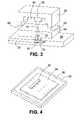
- FIG. 3An embodiment of the packaging arrangement of the present invention is shown in FIG. 3 .
- a ceramic photodetector carrier 50shown without its front wall, houses a commercially available InGaAs photodetector array 52 .
- the arrayhas a plurality of separate photodiodes, at least corresponding in number to the number of taps (not shown in FIG. 3 ) on the associated planar lightwave circuit 54 .
- the upper major surface of the circuit 54extends along the cavity defined by the walls of the carrier 50 and is separated from the cavity by a collimating faceplate 56 .
- the faceplate 56is at least co-extensive with the bottom walls 58 of the carrier 50 and is shaped to match the walls 58 to provide a sealed cover for the cavity 60 of the carrier 50 .
- the faceplatehas a planar surface facing the cavity and the bottom walls 58 of the carrier 50 define a plane, but other surface configurations are also feasible provided that the faceplate 56 matches the bottom walls to provided a sealing cover for the cavity 60 .
- the faceplatemay be manufactured according to any of known techniques, for example as per the U.S. Pat. No. 6,160,606 (Sprague).
- the cavity 60 housing the photodetector array 52may be filled with air or another gas, e.g. an inert gas, and should be free from deleterious contaminants jeopardizing the functioning of the photodetector array as explained above.
- air or another gase.g. an inert gas
- the planar lightwave circuit 54includes a number of channel waveguides as illustrated in FIG. 1 . Only one waveguide section (arm) 20 is shown schematically in FIG. 3 .
- a V-groove 70is formed by etching in the PLC 54 in the path of the arm 20 .
- the left-side wall of the V-grooveis transmissive, while the right-side wall, disposed at 45° to the propagation axis of the arm 20 has a reflective surface formed by sputtering of a metal layer 73 .
- light propagating from the left in the waveguide arm 20passes through the left wall of the V-groove and reflects from the right wall of the V-groove upwards i.e. towards the photodetector array via a core area 72 (indicated in phantom lines) of the faceplate 54 .
- FIG. 4An exemplary finished PLC package, or assembly, of the invention is represented schematically in FIG. 4 .
- a conventional sealing compound or alloye.g. a known Au/Sn alloy, may be applied at the matching surfaces of the faceplate 56 and the carrier 50 .
- the photodetector array 52is thus sealed in the cavity 60 , with its electric leads (not illustrated) arranged in a manner not affecting the hermetic seal.
- the components of the assembly illustrated in FIG. 4are dimensioned such that the spacing between the faceplate 56 and the photodetector 52 is small, e.g. about 0.2 mm, to limit the effect of the inevitable divergence of light emerging from the faceplate towards the photodetector, as represented by the dashed lines in FIG. 4 .
- the spacingshould not be too small to alleviate the risk of contact between the faceplate and the photodetector with associated possibility of losing the seal between the faceplate and the photodetector substrate and a damage to the photodetector.
- the PLC 54may be positively attached to the faceplate 56 using an adhesive, e.g. a known UV (epoxy) adhesive, having a refractive index matched to the refractive index of the cores of the faceplate.
- an adhesivee.g. a known UV (epoxy) adhesive, having a refractive index matched to the refractive index of the cores of the faceplate.
- a bond line thicknessof about 10 ⁇ m or less is used.
- the PLC 54is disposed differently than in FIG. 4 .
- the major surface of the PLC 54 with the waveguides 20is disposed transversely or approximately orthogonally (in a wide range of angles) relative to the major surface 80 of the faceplate 56 , so that the PLC faces the faceplate with its side rather than the major surface.
- This arrangementallows for one or more of the output ends 82 of the waveguides 20 , the ends defining output ports of the respective waveguides, to be aligned with respective core areas of the faceplate 56 and thus with respective photodetectors, without using taps.
- FIG. 1the embodiment illustrated in FIG.
- the waveguides 20terminate with output ends (serving as input ports within the meaning of the present invention) such that the entire signal propagating in one of the waveguides is coupled out of the PLC through the output end (port) 82 .
- the waveguidesmay have couplers as illustrated in FIG. 1 except that all the coupler arms may terminate at the same edge of the PLC.
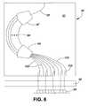
- FIG. 6where the PLC 54 of FIG. 5 is represented by an arrayed waveguide grating (AWG) 90 arranged with its major surface 92 perpendicularly to the faceplate 56 .
- the photodetector arrayis indicated schematically as 94 .
- the AWGarranged as a demultiplexer, has an input waveguide 96 , a slab waveguide 97 , an array waveguide portion 98 , a slab waveguide 99 and a plurality of output optical waveguides 100 .
- the output optical waveguides, or at least some of them,have directional couplers 102 serving as taps, wherein a tapped portion of light propagating in the output waveguide is directed to a respective photodetector in the array 94 , while the rest of the light is coupled to a destination, not shown.
- the destinationmay be the edge of the PLC, where the light will be coupled into a fiber or into a free space optical device, not illustrated.
- the collimating plateallows a majority of each photodetector element to be filled with light while not over-filling to the point of losing light or causing adjacent photodetector elements to pick up light from a single source.
- the spacing between the collimating plate and the photodetectorscan be selected to enable the use of photodetector arrays with varying element diameters. Closer spacing can be used to create a smaller light spot size for smaller photodetectors. Larger spacing can be used to fill larger elements in photodetector arrays where higher sensitivity is needed. Smaller diameter PD elements tend to be less sensitive but offer greater speed and lower electrical noise.
- the use of the collimating plateprovides a highly reliable hermetic package window without affecting the light beams that are directed towards the photodetector elements.
- the collimating faceplateprevents excessive beam divergence or beam angle changes which are key advantages in the packaging of photodetector arrays designed for the purpose of monitoring light emerging from multiple waveguides in a PLC circuit.
- the collimating faceplatecan also enable free-space optical coupling to a photodetector array where direct bonding to a PLC is not an option. This can be done by placing the collimating faceplate very close (e.g. in a range of a few ⁇ m to a few hundred ⁇ m) but not in contact with the photodetector array. Up to 200 ⁇ m of spacing can then be allowed between the outside surface of the collimating plate (package) and the free-space light source. This spacing must be adjusted to match the photodetector element diameter in a way that is similar to the tuning techniques described hereinabove. As indicated above, the invention applicable to various arrays of optical input ports, such as liquid crystal displays (LCD) or laser diode (LD) arrays. FIG. 5 represents schematically, mutatis mutandis, such other arrangements wherein the element 54 represents a specific fixed array of optical input ports.
- LCDliquid crystal displays
- LDlaser diode
- the inventioneliminates the cumbersome fiber pigtailing to photodetectors.
- the spacing of the photodetectors in the PD arraycan be relatively close to accommodate closely spaced monitor waveguides on the associated PLC.
Landscapes
- Physics & Mathematics (AREA)
- Engineering & Computer Science (AREA)
- Microelectronics & Electronic Packaging (AREA)
- General Physics & Mathematics (AREA)
- Optics & Photonics (AREA)
- Optical Couplings Of Light Guides (AREA)
- Optical Integrated Circuits (AREA)
- Semiconductor Lasers (AREA)
Abstract
Description
Claims (1)
Priority Applications (1)
| Application Number | Priority Date | Filing Date | Title |
|---|---|---|---|
| US11/200,696US7203390B2 (en) | 2003-02-18 | 2005-08-10 | Planar lightwave circuit package |
Applications Claiming Priority (2)
| Application Number | Priority Date | Filing Date | Title |
|---|---|---|---|
| US10/368,195US6945708B2 (en) | 2003-02-18 | 2003-02-18 | Planar lightwave circuit package |
| US11/200,696US7203390B2 (en) | 2003-02-18 | 2005-08-10 | Planar lightwave circuit package |
Related Parent Applications (1)
| Application Number | Title | Priority Date | Filing Date |
|---|---|---|---|
| US10/368,195DivisionUS6945708B2 (en) | 2003-02-18 | 2003-02-18 | Planar lightwave circuit package |
Publications (2)
| Publication Number | Publication Date |
|---|---|
| US20060034561A1 US20060034561A1 (en) | 2006-02-16 |
| US7203390B2true US7203390B2 (en) | 2007-04-10 |
Family
ID=32850118
Family Applications (2)
| Application Number | Title | Priority Date | Filing Date |
|---|---|---|---|
| US10/368,195Expired - Fee RelatedUS6945708B2 (en) | 2003-02-18 | 2003-02-18 | Planar lightwave circuit package |
| US11/200,696Expired - LifetimeUS7203390B2 (en) | 2003-02-18 | 2005-08-10 | Planar lightwave circuit package |
Family Applications Before (1)
| Application Number | Title | Priority Date | Filing Date |
|---|---|---|---|
| US10/368,195Expired - Fee RelatedUS6945708B2 (en) | 2003-02-18 | 2003-02-18 | Planar lightwave circuit package |
Country Status (2)
| Country | Link |
|---|---|
| US (2) | US6945708B2 (en) |
| JP (1) | JP2004252454A (en) |
Cited By (1)
| Publication number | Priority date | Publication date | Assignee | Title |
|---|---|---|---|---|
| CN105044860A (en)* | 2015-06-24 | 2015-11-11 | 湖南晶图科技有限公司 | Wafer processing technique for vertically integrating PLC waveguide with infrared receiver |
Families Citing this family (12)
| Publication number | Priority date | Publication date | Assignee | Title |
|---|---|---|---|---|
| US6981806B2 (en)* | 2002-07-05 | 2006-01-03 | Xponent Photonics Inc | Micro-hermetic packaging of optical devices |
| US20040183003A1 (en)* | 2003-03-21 | 2004-09-23 | Mohammad Eslamy | Localized hermetic sealing of a power monitor on a planar light circuit |
| WO2004097474A1 (en)* | 2003-04-29 | 2004-11-11 | Xponent Photonics Inc | Surface-mounted photodetector for an optical waveguide |
| JP4550377B2 (en)* | 2003-06-25 | 2010-09-22 | オリンパス株式会社 | Imaging device |
| US7272273B2 (en)* | 2005-01-21 | 2007-09-18 | Neophotonics Corporation | Photodetector coupled to a planar waveguide |
| CN102494776B (en)* | 2007-04-03 | 2014-11-19 | 武藤工业株式会社 | Spectrophotometer and method |
| KR101515732B1 (en)* | 2010-10-07 | 2015-04-27 | 알까뗄 루슨트 | Opto-electronic assembly for a line card |
| US8478086B2 (en)* | 2011-03-02 | 2013-07-02 | Eastman Kodak Company | Imaging laser diodes with a lightwave circuit |
| US10713675B2 (en) | 2012-09-28 | 2020-07-14 | Intel Corporation | Systems and methods for generation of incentive offers for on-road users |
| US10042116B2 (en) | 2016-04-25 | 2018-08-07 | Applied Optoelectronics, Inc. | Techniques for direct optical coupling of photodetectors to optical demultiplexer outputs and an optical transceiver using the same |
| CN105866904A (en)* | 2016-05-23 | 2016-08-17 | 宁波环球广电科技有限公司 | Multichannel parallel optical receiving device |
| CN206920661U (en) | 2017-07-13 | 2018-01-23 | 宁波环球广电科技有限公司 | High Speeding Optical Transmitter-receiver Circuit |
Citations (9)
| Publication number | Priority date | Publication date | Assignee | Title |
|---|---|---|---|---|
| US5170455A (en) | 1991-10-30 | 1992-12-08 | At&T Bell Laboratories | Optical connective device |
| US5586207A (en) | 1993-11-29 | 1996-12-17 | Northern Telecom Limited | Methods and assemblies for packaging opto-electronic devices and for coupling optical fibers to the packaged devices |
| US6137929A (en) | 1999-02-11 | 2000-10-24 | Agilent Technologies, Inc. | System and method for interfacing optical fibers with optical communications devices via an optical fiber faceplate |
| US6160606A (en) | 1997-08-05 | 2000-12-12 | Xerox Corporation | Optical equivalents of fiber optic face plates using irradiation sensitive glass |
| US6238100B1 (en) | 1998-10-21 | 2001-05-29 | Nec Corporation | Optical module and a method for fabricating a same |
| US6318909B1 (en) | 1999-02-11 | 2001-11-20 | Agilent Technologies, Inc. | Integrated packaging system for optical communications devices that provides automatic alignment with optical fibers |
| WO2002039155A2 (en) | 2000-11-06 | 2002-05-16 | Schott Communications Technologies, Inc. | Fiber optic faceplate |
| US6507680B1 (en) | 1999-09-14 | 2003-01-14 | Sumitomo Electric Industries, Ltd. | Planar lightwave circuit module |
| US6901185B2 (en)* | 2002-01-15 | 2005-05-31 | Nec Corporation | Optical module capable of improving coupling efficiency and suppressing fluctuation of coupling loss and its manufacturing method |
Family Cites Families (9)
| Publication number | Priority date | Publication date | Assignee | Title |
|---|---|---|---|---|
| JPS57103405U (en)* | 1980-12-15 | 1982-06-25 | ||
| US4828358A (en)* | 1988-03-03 | 1989-05-09 | American Telephone And Telegraph Company, At&T Bell Laboratories | Testing in the manufacture, operation, and maintenance of optical device assemblies |
| JPH0266746A (en)* | 1988-08-31 | 1990-03-06 | Brother Ind Ltd | optical head |
| JPH06324224A (en)* | 1993-05-11 | 1994-11-25 | Furukawa Electric Co Ltd:The | Waveguide type device |
| JPH10126002A (en)* | 1996-10-23 | 1998-05-15 | Matsushita Electron Corp | Optical transmission module |
| JP3427966B2 (en)* | 1997-07-08 | 2003-07-22 | 日本電信電話株式会社 | Method for aligning optical waveguide circuit and input / output optical fiber and optical waveguide circuit mounting apparatus |
| JPH1184183A (en)* | 1997-09-12 | 1999-03-26 | Nippon Telegr & Teleph Corp <Ntt> | Optical module |
| JP4667558B2 (en)* | 2000-05-26 | 2011-04-13 | 古河電気工業株式会社 | Optical system using optical modules |
| WO2002073256A1 (en)* | 2001-02-28 | 2002-09-19 | Nec Corporation | Optical circuit element and production method therefor, array-form optical circuit element, optical circuit device using it |
- 2003
- 2003-02-18USUS10/368,195patent/US6945708B2/ennot_activeExpired - Fee Related
- 2004
- 2004-02-16JPJP2004039094Apatent/JP2004252454A/enactivePending
- 2005
- 2005-08-10USUS11/200,696patent/US7203390B2/ennot_activeExpired - Lifetime
Patent Citations (9)
| Publication number | Priority date | Publication date | Assignee | Title |
|---|---|---|---|---|
| US5170455A (en) | 1991-10-30 | 1992-12-08 | At&T Bell Laboratories | Optical connective device |
| US5586207A (en) | 1993-11-29 | 1996-12-17 | Northern Telecom Limited | Methods and assemblies for packaging opto-electronic devices and for coupling optical fibers to the packaged devices |
| US6160606A (en) | 1997-08-05 | 2000-12-12 | Xerox Corporation | Optical equivalents of fiber optic face plates using irradiation sensitive glass |
| US6238100B1 (en) | 1998-10-21 | 2001-05-29 | Nec Corporation | Optical module and a method for fabricating a same |
| US6137929A (en) | 1999-02-11 | 2000-10-24 | Agilent Technologies, Inc. | System and method for interfacing optical fibers with optical communications devices via an optical fiber faceplate |
| US6318909B1 (en) | 1999-02-11 | 2001-11-20 | Agilent Technologies, Inc. | Integrated packaging system for optical communications devices that provides automatic alignment with optical fibers |
| US6507680B1 (en) | 1999-09-14 | 2003-01-14 | Sumitomo Electric Industries, Ltd. | Planar lightwave circuit module |
| WO2002039155A2 (en) | 2000-11-06 | 2002-05-16 | Schott Communications Technologies, Inc. | Fiber optic faceplate |
| US6901185B2 (en)* | 2002-01-15 | 2005-05-31 | Nec Corporation | Optical module capable of improving coupling efficiency and suppressing fluctuation of coupling loss and its manufacturing method |
Cited By (1)
| Publication number | Priority date | Publication date | Assignee | Title |
|---|---|---|---|---|
| CN105044860A (en)* | 2015-06-24 | 2015-11-11 | 湖南晶图科技有限公司 | Wafer processing technique for vertically integrating PLC waveguide with infrared receiver |
Also Published As
| Publication number | Publication date |
|---|---|
| JP2004252454A (en) | 2004-09-09 |
| US6945708B2 (en) | 2005-09-20 |
| US20040161186A1 (en) | 2004-08-19 |
| US20060034561A1 (en) | 2006-02-16 |
Similar Documents
| Publication | Publication Date | Title |
|---|---|---|
| US7532778B2 (en) | Optical waveguide modulator equipped with an output light monitor | |
| US6406196B1 (en) | Optical device and method for producing the same | |
| US8639073B2 (en) | Fiber coupling technique on a waveguide | |
| CA2033543C (en) | Optical fiber electro-optical module | |
| US5499309A (en) | Method of fabricating optical component including first and second optical waveguide chips having opposed inclined surfaces | |
| US7106980B2 (en) | Optical receiver | |
| EP0404301B1 (en) | Optoelectronic apparatus and method for its fabrication | |
| US5497438A (en) | Optical transmission and reception module having coupled optical waveguide chips | |
| US7203390B2 (en) | Planar lightwave circuit package | |
| US7561764B2 (en) | Integrated reflector for planar lightwave circuits | |
| KR100897887B1 (en) | Hybrid Integrated Structure of Planar Optical Waveguide Device and Active Device Using Fiber Array | |
| JP2002131586A (en) | Optical communication module and manufacturing method thereof | |
| US20060013541A1 (en) | Optoelectronic module | |
| EP1415185A1 (en) | High density fibre coupling | |
| WO2003060584A1 (en) | Optical waveguide module | |
| US20030002799A1 (en) | Optical coupling configuration | |
| US7266270B2 (en) | Waveguide to waveguide monitor | |
| KR101501140B1 (en) | Planar Lightwave Circuit Module Having an Improved Structure of an Optical Power Monitor | |
| JPH0961678A (en) | Semiconductor light receiving element | |
| KR101227039B1 (en) | Optical power monitoring module | |
| JP2005134803A (en) | Ferrule with optical isolator and optical transmission/reception module equipped with the same | |
| KR101216732B1 (en) | Optical power monitoring module using the thin flexible pcb, and the manufacturing method | |
| KR101220303B1 (en) | Optical power monitoring module | |
| KR101501139B1 (en) | Planar Lightwave Circuit Module having an improved Structure of an Optical Power Monitor | |
| KR101048428B1 (en) | Optical waveguide optical module |
Legal Events
| Date | Code | Title | Description |
|---|---|---|---|
| STCF | Information on status: patent grant | Free format text:PATENTED CASE | |
| FPAY | Fee payment | Year of fee payment:4 | |
| FPAY | Fee payment | Year of fee payment:8 | |
| AS | Assignment | Owner name:LUMENTUM OPERATIONS LLC, CALIFORNIA Free format text:ASSIGNMENT OF ASSIGNORS INTEREST;ASSIGNOR:JDS UNIPHASE CORPORATION;REEL/FRAME:036420/0340 Effective date:20150731 | |
| FEPP | Fee payment procedure | Free format text:PAYOR NUMBER ASSIGNED (ORIGINAL EVENT CODE: ASPN); ENTITY STATUS OF PATENT OWNER: LARGE ENTITY | |
| AS | Assignment | Owner name:LUMENTUM OPERATIONS LLC, CALIFORNIA Free format text:CORRECTIVE ASSIGNMENT TO CORRECT THE PATENTS LISTED ON PAGE A-A33 PREVIOUSLY RECORDED ON REEL 036420 FRAME 0340. ASSIGNOR(S) HEREBY CONFIRMS THE PATENT NUMBERS 7,868,247 AND 6,476,312 WERE LISTED IN ERROR AND SHOULD BE REMOVED;ASSIGNOR:JDS UNIPHASE CORPORATION;REEL/FRAME:037562/0513 Effective date:20150731 Owner name:LUMENTUM OPERATIONS LLC, CALIFORNIA Free format text:CORRECTIVE ASSIGNMENT TO CORRECT INCORRECT PATENTS 7,868,247 AND 6,476,312 ON PAGE A-A33 PREVIOUSLY RECORDED ON REEL 036420 FRAME 0340. ASSIGNOR(S) HEREBY CONFIRMS THE ASSIGNMENT;ASSIGNOR:JDS UNIPHASE CORPORATION;REEL/FRAME:037562/0513 Effective date:20150731 | |
| AS | Assignment | Owner name:LUMENTUM OPERATIONS LLC, CALIFORNIA Free format text:CORRECTIVE ASSIGNMENT TO CORRECT THE PATENTS LISTED ON PAGE A-A33 PATENT NUMBERS 7,868,247 AND 6,476,312 WERE LISTED IN ERROR AND SHOULD BE REMOVED. PREVIOUSLY RECORDED ON REEL 036420 FRAME 0340. ASSIGNOR(S) HEREBY CONFIRMS THE ASSIGNMENT;ASSIGNOR:JDS UNIPHASE CORPORATION;REEL/FRAME:037627/0641 Effective date:20150731 Owner name:LUMENTUM OPERATIONS LLC, CALIFORNIA Free format text:CORRECTIVE ASSIGNMENT TO CORRECT PATENTS 7,868,247 AND 6,476,312 LISTED ON PAGE A-A33 PREVIOUSLY RECORDED ON REEL 036420 FRAME 0340. ASSIGNOR(S) HEREBY CONFIRMS THE ASSIGNMENT;ASSIGNOR:JDS UNIPHASE CORPORATION;REEL/FRAME:037627/0641 Effective date:20150731 | |
| FEPP | Fee payment procedure | Free format text:PAYER NUMBER DE-ASSIGNED (ORIGINAL EVENT CODE: RMPN); ENTITY STATUS OF PATENT OWNER: LARGE ENTITY Free format text:PAYOR NUMBER ASSIGNED (ORIGINAL EVENT CODE: ASPN); ENTITY STATUS OF PATENT OWNER: LARGE ENTITY | |
| MAFP | Maintenance fee payment | Free format text:PAYMENT OF MAINTENANCE FEE, 12TH YEAR, LARGE ENTITY (ORIGINAL EVENT CODE: M1553); ENTITY STATUS OF PATENT OWNER: LARGE ENTITY Year of fee payment:12 | |
| AS | Assignment | Owner name:DEUTSCHE BANK AG NEW YORK BRANCH, AS COLLATERAL AGENT, NEW YORK Free format text:PATENT SECURITY AGREEMENT;ASSIGNORS:LUMENTUM OPERATIONS LLC;OCLARO FIBER OPTICS, INC.;OCLARO, INC.;REEL/FRAME:047788/0511 Effective date:20181210 Owner name:DEUTSCHE BANK AG NEW YORK BRANCH, AS COLLATERAL AG Free format text:PATENT SECURITY AGREEMENT;ASSIGNORS:LUMENTUM OPERATIONS LLC;OCLARO FIBER OPTICS, INC.;OCLARO, INC.;REEL/FRAME:047788/0511 Effective date:20181210 | |
| AS | Assignment | Owner name:OCLARO FIBER OPTICS, INC., CALIFORNIA Free format text:RELEASE BY SECURED PARTY;ASSIGNOR:DEUTSCHE AG NEW YORK BRANCH;REEL/FRAME:051287/0556 Effective date:20191212 Owner name:LUMENTUM OPERATIONS LLC, CALIFORNIA Free format text:RELEASE BY SECURED PARTY;ASSIGNOR:DEUTSCHE AG NEW YORK BRANCH;REEL/FRAME:051287/0556 Effective date:20191212 Owner name:OCLARO, INC., CALIFORNIA Free format text:RELEASE BY SECURED PARTY;ASSIGNOR:DEUTSCHE AG NEW YORK BRANCH;REEL/FRAME:051287/0556 Effective date:20191212 |