US7203283B1 - X-ray tube of the end window type, and an X-ray fluorescence analyzer - Google Patents
X-ray tube of the end window type, and an X-ray fluorescence analyzerDownload PDFInfo
- Publication number
- US7203283B1 US7203283B1US11/358,835US35883506AUS7203283B1US 7203283 B1US7203283 B1US 7203283B1US 35883506 AUS35883506 AUS 35883506AUS 7203283 B1US7203283 B1US 7203283B1
- Authority
- US
- United States
- Prior art keywords
- anode layer
- anode
- layer
- ray tube
- ray
- Prior art date
- Legal status (The legal status is an assumption and is not a legal conclusion. Google has not performed a legal analysis and makes no representation as to the accuracy of the status listed.)
- Active
Links
- 238000004876x-ray fluorescenceMethods0.000titleclaimsdescription9
- 239000000463materialSubstances0.000claimsdescription26
- 230000005461BremsstrahlungEffects0.000claimsdescription14
- WFKWXMTUELFFGS-UHFFFAOYSA-NtungstenChemical compound[W]WFKWXMTUELFFGS-UHFFFAOYSA-N0.000claimsdescription14
- 229910052721tungstenInorganic materials0.000claimsdescription14
- 239000010937tungstenSubstances0.000claimsdescription14
- 239000000470constituentSubstances0.000claimsdescription11
- 230000005855radiationEffects0.000claimsdescription11
- 229910052703rhodiumInorganic materials0.000claimsdescription11
- 239000010948rhodiumSubstances0.000claimsdescription11
- MHOVAHRLVXNVSD-UHFFFAOYSA-Nrhodium atomChemical compound[Rh]MHOVAHRLVXNVSD-UHFFFAOYSA-N0.000claimsdescription11
- 238000012545processingMethods0.000claimsdescription10
- 230000003595spectral effectEffects0.000claimsdescription7
- KDLHZDBZIXYQEI-UHFFFAOYSA-NPalladiumChemical compound[Pd]KDLHZDBZIXYQEI-UHFFFAOYSA-N0.000claimsdescription6
- 229910052790berylliumInorganic materials0.000claimsdescription6
- ATBAMAFKBVZNFJ-UHFFFAOYSA-Nberyllium atomChemical compound[Be]ATBAMAFKBVZNFJ-UHFFFAOYSA-N0.000claimsdescription6
- 238000001914filtrationMethods0.000claimsdescription6
- 230000035515penetrationEffects0.000claimsdescription6
- BASFCYQUMIYNBI-UHFFFAOYSA-NplatinumChemical compound[Pt]BASFCYQUMIYNBI-UHFFFAOYSA-N0.000claimsdescription6
- 229910052804chromiumInorganic materials0.000claimsdescription5
- 239000011651chromiumSubstances0.000claimsdescription5
- 229910052802copperInorganic materials0.000claimsdescription5
- 239000010949copperSubstances0.000claimsdescription5
- 229910052709silverInorganic materials0.000claimsdescription5
- 239000004332silverSubstances0.000claimsdescription5
- VYZAMTAEIAYCRO-UHFFFAOYSA-NChromiumChemical compound[Cr]VYZAMTAEIAYCRO-UHFFFAOYSA-N0.000claimsdescription4
- RYGMFSIKBFXOCR-UHFFFAOYSA-NCopperChemical compound[Cu]RYGMFSIKBFXOCR-UHFFFAOYSA-N0.000claimsdescription4
- ZOKXTWBITQBERF-UHFFFAOYSA-NMolybdenumChemical compound[Mo]ZOKXTWBITQBERF-UHFFFAOYSA-N0.000claimsdescription4
- 238000013507mappingMethods0.000claimsdescription4
- 238000000034methodMethods0.000claimsdescription4
- 229910052750molybdenumInorganic materials0.000claimsdescription4
- 239000011733molybdenumSubstances0.000claimsdescription4
- BQCADISMDOOEFD-UHFFFAOYSA-NSilverChemical compound[Ag]BQCADISMDOOEFD-UHFFFAOYSA-N0.000claimsdescription3
- 229910052735hafniumInorganic materials0.000claimsdescription3
- VBJZVLUMGGDVMO-UHFFFAOYSA-Nhafnium atomChemical compound[Hf]VBJZVLUMGGDVMO-UHFFFAOYSA-N0.000claimsdescription3
- 229910052763palladiumInorganic materials0.000claimsdescription3
- 229910052697platinumInorganic materials0.000claimsdescription3
- 230000008569processEffects0.000claimsdescription3
- 229910052702rheniumInorganic materials0.000claimsdescription3
- WUAPFZMCVAUBPE-UHFFFAOYSA-Nrhenium atomChemical compound[Re]WUAPFZMCVAUBPE-UHFFFAOYSA-N0.000claimsdescription3
- 239000010405anode materialSubstances0.000description17
- 238000001228spectrumMethods0.000description7
- 238000000695excitation spectrumMethods0.000description6
- 229910052793cadmiumInorganic materials0.000description5
- BDOSMKKIYDKNTQ-UHFFFAOYSA-Ncadmium atomChemical compound[Cd]BDOSMKKIYDKNTQ-UHFFFAOYSA-N0.000description5
- 238000005259measurementMethods0.000description5
- 230000008901benefitEffects0.000description4
- 229910001385heavy metalInorganic materials0.000description4
- 239000002689soilSubstances0.000description4
- 230000005540biological transmissionEffects0.000description3
- 230000005284excitationEffects0.000description3
- 230000003993interactionEffects0.000description3
- PXHVJJICTQNCMI-UHFFFAOYSA-NNickelChemical compound[Ni]PXHVJJICTQNCMI-UHFFFAOYSA-N0.000description2
- 230000001133accelerationEffects0.000description2
- 238000004458analytical methodMethods0.000description2
- 238000001514detection methodMethods0.000description2
- 230000005684electric fieldEffects0.000description2
- 239000003344environmental pollutantSubstances0.000description2
- 230000005281excited stateEffects0.000description2
- 239000011159matrix materialSubstances0.000description2
- 229910052751metalInorganic materials0.000description2
- 239000002184metalSubstances0.000description2
- 239000002245particleSubstances0.000description2
- 231100000719pollutantToxicity0.000description2
- 239000013077target materialSubstances0.000description2
- 238000002083X-ray spectrumMethods0.000description1
- 238000010521absorption reactionMethods0.000description1
- 238000005275alloyingMethods0.000description1
- 238000013459approachMethods0.000description1
- 230000008859changeEffects0.000description1
- 230000001427coherent effectEffects0.000description1
- 239000004020conductorSubstances0.000description1
- 238000010276constructionMethods0.000description1
- 238000009826distributionMethods0.000description1
- 230000000694effectsEffects0.000description1
- 238000000295emission spectrumMethods0.000description1
- 238000012921fluorescence analysisMethods0.000description1
- 229910052737goldInorganic materials0.000description1
- 239000010931goldSubstances0.000description1
- 238000010438heat treatmentMethods0.000description1
- 239000008240homogeneous mixtureSubstances0.000description1
- 239000012535impuritySubstances0.000description1
- 229910052742ironInorganic materials0.000description1
- XEEYBQQBJWHFJM-UHFFFAOYSA-NironSubstances[Fe]XEEYBQQBJWHFJM-UHFFFAOYSA-N0.000description1
- 238000004519manufacturing processMethods0.000description1
- 239000000203mixtureSubstances0.000description1
- 238000003900soil pollutionMethods0.000description1
- 229910052715tantalumInorganic materials0.000description1
- 229910052719titaniumInorganic materials0.000description1
- 239000010936titaniumSubstances0.000description1
- 230000007704transitionEffects0.000description1
Images

Classifications
- H—ELECTRICITY
- H01—ELECTRIC ELEMENTS
- H01J—ELECTRIC DISCHARGE TUBES OR DISCHARGE LAMPS
- H01J35/00—X-ray tubes
- H01J35/02—Details
- H01J35/04—Electrodes ; Mutual position thereof; Constructional adaptations therefor
- H01J35/08—Anodes; Anti cathodes
- H01J35/112—Non-rotating anodes
- H01J35/116—Transmissive anodes
- H—ELECTRICITY
- H01—ELECTRIC ELEMENTS
- H01J—ELECTRIC DISCHARGE TUBES OR DISCHARGE LAMPS
- H01J35/00—X-ray tubes
- H01J35/02—Details
- H01J35/16—Vessels; Containers; Shields associated therewith
- H01J35/18—Windows
- H01J35/186—Windows used as targets or X-ray converters
- H—ELECTRICITY
- H01—ELECTRIC ELEMENTS
- H01J—ELECTRIC DISCHARGE TUBES OR DISCHARGE LAMPS
- H01J2235/00—X-ray tubes
- H01J2235/08—Targets (anodes) and X-ray converters
- H01J2235/081—Target material
- H—ELECTRICITY
- H01—ELECTRIC ELEMENTS
- H01J—ELECTRIC DISCHARGE TUBES OR DISCHARGE LAMPS
- H01J2235/00—X-ray tubes
- H01J2235/08—Targets (anodes) and X-ray converters
- H01J2235/088—Laminated targets, e.g. plurality of emitting layers of unique or differing materials
- H—ELECTRICITY
- H01—ELECTRIC ELEMENTS
- H01J—ELECTRIC DISCHARGE TUBES OR DISCHARGE LAMPS
- H01J2235/00—X-ray tubes
- H01J2235/18—Windows, e.g. for X-ray transmission
- H01J2235/183—Multi-layer structures
Definitions
- the inventionconcerns the technical field of controllable x-ray sources that are applicable for use e.g. in measurement systems where X-rays are needed as excitation radiation. Especially the invention concerns adapting the structure of an X-ray tube to comply with requirements of producing radiation of a particular kind.
- An X-ray tubeis a controllable X-ray source, in which electrons detached from a cathode get accelerated in an electric field and hit an anode, where they lose their kinetic energy in various interaction processes with the atoms of the anode material.
- One result of these interaction processesis the generation of X-rays, the spectrum of which comprises both a continuous part (known as bremsstrahlung) and some prominent peaks.
- the energies at which the peaks occurdepend on the anode material, because the peaks are associated with the relaxation of excited states in the atoms of the anode.
- Widely used anode materialsare include (without being limited to) chromium, copper, molybdenum, rhodium, silver and tungsten.
- the spectral distribution and intensity of the bremsstrahlung partis proportional to both the acceleration voltage and the atomic ordinal number of the anode material: higher acceleration voltages and heavier anode materials increase the intensity of the continuous spectrum part at
- An X-ray tubeis either of the bulk anode type or of the transmission anode type.
- a bulk anodeis relatively thick and typically designed to direct the generated X-rays out of a separate window in a side surface of the X-ray tube, for which reason also the designation “side window type” is used for these kinds of X-ray tubes.
- a transmission anodeis thin enough to let the generated X-rays pass through it.
- a transmission anodeis typically a thin metal layer on an inner surface of an end window of the X-ray tube, giving rise to the alternative designation “end window type” X-ray tube.
- the bremsstrahlung part and peak parts of the excitation spectrumare useful for different purposes for example in X-ray fluorescence analysis, in which the incident X-rays coming from an X-ray tube in turn excite the constituent particles of a target material.
- the fluorescence analysisinvolves detecting the fluorescent X-rays that come from the relaxation of excited states in said constituent particles, and using the detection results to make deductions about the presence of various elements in the target.
- the targetmay be very heterogeneous in constitution, like a soil sample from which the content of heavy metal pollutants should be measured.
- the characteristic peaks in the excitation radiationare useful for determining the matrix of ordinary soil constituents, while the high-energy bremsstrahlung part of the spectrum suitably excites the atoms of the heavy metals like lead, cadmium and others.
- anode materialthat gives good characteristic peaks does not necessarily give enough bremsstrahlung in the desired energy ranges.
- rhodiumas anode material.
- K lines of rhodiumare easily applicable to determining the ratio between coherent scattering and Compton scattering, which enables using effective analytical tools for determining the matrix of a sample, such as soil.
- the amount of bremsstrahlung coming from a rhodium anodeis relatively low in the frequency range that would be required to properly excite the atoms of cadmium, which is a typical pollutant to be measured from soil.
- the intensity of fluorescent radiation that can be obtained from a target materialis proportional to the intensity of excitation radiation in the proper frequency range.
- a rhodium anoderesults in a relatively low intensity of fluorescent radiation from cadmium and other heavy metals, which weakens the analytical performance of the X-ray fluorescence analyzer in measuring soil pollution.
- a layered anode structurein which a carrier layer supports at least two anode layers made of anode materials with a difference in atomic ordinal number.
- anode layerby using two anode layers and suitable dimensioning it is possible to achieve a situation, in which some of the accelerated electrons interact within a “heavy” anode layer producing a relatively high amount of bremsstrahlung, while others interact with a “light” anode layer producing at least one prominent characteristic peak at a spectral location characteristic to that anode material.
- Characterising the other anode material as “light” onlyindicates that its atomic ordinal number is smaller than that of the “heavy” anode material; typically the “light” anode material could be for example rhodium, palladium, chromium, copper or molybdenum. Also silver can be used as the “light” anode material, if the measurement is not meant to detect cadmium, this condition being due to certain coincidences in the spectral characteristic of silver and cadmium. Suitable materials for use as the “heavy” anode material are for example tungsten, hafnium, platinum and rhenium.
- An X-ray fluorescence analyzercomprises an end window type X-ray tube, in which the anode is of the multilayer type described above and in which the detection and processing parts are adapted to take advantage of the special form of the resulting excitation spectrum.
- FIG. 1illustrates an X-ray tube
- FIG. 2illustrates an X-ray fluorescence analyzer
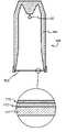
- FIG. 1is a schematic cross section of an X-ray tube 100 of the end window type.
- An airtight housing 101is designed to maintain essentially vacuum conditions inside it.
- a cathode arrangement 102designed to emit electrons, for example as the result of heating up a cathode wire coupled to a high negative voltage.
- an end windowwhich is generally designated as 103 .
- the end window 103has a layered structure.
- a carrier layer 111is made of a material that is mechanically strong, chemically stable and permeable to X-rays.
- a preferred material for the carrier layer 111is beryllium, but also other materials can be used that are known for their suitability for radiation-passing windows of X-ray tubes.
- first anode layer 112On the inner surface of the carrier layer 111 there is a layered anode arrangement. A strong electric field between the cathode arrangement 102 and the anode arrangement, caused by the large potential difference between them, is adapted to accelerate the electrons emitted by the cathode arrangement 102 so that they hit the layered anode arrangement.
- the layer immediately on top of the carrier layer 111is a first anode layer 112 , which corresponds to the “light” anode layer mentioned previously in this description. In order to function as an anode layer it must be made of an electrically conductive material. An even more important characteristic of the first anode layer 112 is that it consists of a material that is known to emit suitable characteristic X-ray lines when subjected to electron bombardment.
- the first anode layer 112is made of rhodium, palladium, chromium, copper, molybdenum or silver.
- the second anode layer 113On top of the first anode layer 112 there is a second anode layer 113 , which is thus the innermost layer of the end window 103 and faces the vacuum inside the housing 101 . Also the second anode layer 113 is electrically conductive, but what is more important, it is made of a material having a larger atomic ordinal number than the material of the first anode layer 112 . Exemplary materials of the second anode layer 113 are tungsten, hafnium, platinum and rhenium.
- the relative thicknesses of the carrier layer 111 on one hand and the first and second anode layers 112 and 113 on the other handdo not correspond to reality in FIG. 1 .
- the thickness of the carrier layer 111has relatively little importance to the radiation-emitting characteristics of the X-ray tube 100 . Accelerated electrons that hit the end window 103 would only penetrate the material of the carrier layer 111 to a maximum depth of some micrometers. Additionally there are the anode layers on top of it, which means that all carrier layer materials of reasonable thickness completely block any electrons from coming through.
- known window materialssuch as beryllium are so transparent to X-rays that even thicknesses of hundreds of micrometers cause practically no absorption at energy levels comparable to the K lines of rhodium, which are a representative example of the X-rays meant here.
- the thickness of the carrier layer 111will be selected mainly to achieve sufficient mechanical strength and sufficiently high thermal conductivity.
- a carrier layer 111 made of berylliumwould typically have a thickness between 150 and 800 micrometers, for example 500 micrometers.
- the thicknesses of the first and second anode layers 112 and 113have very much influence to the radiation-emitting characteristics of the X-ray tube 100 .
- the accelerated electronswill hit first the second anode layer 113 , which is the “heavy” layer, the task of which is to give rise to high-energy bremsstrahlung of sufficient intensity.
- not all accelerated electronsshould interact within the second anode layer 113 , but a significant portion should continue to the first, “light” anode layer 112 to generate the characteristic peaks in the excitation spectrum. This means that the thickness of the second, “heavy” anode layer 113 should be remarkably smaller than the maximum penetration depth of accelerated electrons in the material thereof.
- tungstenis used as the material of the second anode layer 113 , its thickness is preferably not more than 0.5 micrometers, and can be less than that.
- a lower limit to the thickness of the second anode layercan be found by experimenting; an optimum is a thickness that gives the best balance between bremsstrahlung intensity and characteristic peak intensity for a particular measurement.
- the thickness of the first layermay be greater than the thickness of the second, “heavy” anode layer 113 . Principally the thicker the layer 112 , the higher intensity of the characteristic peaks will result. However, there is an upper limit concerning this intensity aspect at the maximum penetration depth of accelerated electrons in the material of the first anode layer. If the first anode layer 112 is made of rhodium, it can have a thickness between 0.8 and 1.0 micrometers.
- first anode layer 112may advocate an even thicker first anode layer 112 . Since the second, “heavy” anode layer 113 is only there to generate bremsstrahlung of sufficiently high energy, it may be advantageous to filter out some other, undesired wavelengths from the eventual emission spectrum. For example, with a second anode layer 113 made of tungsten, the value of the voltage that accelerates the electrons will be deliberately selected low enough not to excite the K lines of tungsten. The L lines of tungsten will be there and get excited, but making the first anode layer 112 thick enough, more than 1.0 micrometers, may filter these out.
- An alternative way of filteringwould be to use a separate output filter, like a nickel foil, at the output of the X-ray tube.
- Separate filtering layerssuch as said nickel foil may be integrated into the layered end window structure either between the first anode layer 112 and the carrier layer 111 or on the outer side of the carrier layer.
- standalone filterscan be used, with their own attachment means that facilitate attaching them to the output end of the X-ray tube 100 .
- anode layeris made of a material
- Minor amounts of impuritieswill always exist in all practical anode layers, and in some cases it may prove to be advantageous to even deliberately use some small amounts of alloying constituents.
- all deliberately added component materialshave to be taken into account in analysing the measurement results, because they will cause corresponding changes in the characteristics of the emitted X-ray spectrum.
- an anode layercomprise two different materials also by using a homogeneous mixture of the “heavy” and “light” materials to produce a single anode layer, or by making patches of the different materials alternate in the anode layer in some kind of a checkerboard or honeycomb pattern.
- such solutionswould not be as advantageous as the one described above that comprises the two anode layers on top of each other, for example because said alternative solutions would not enable using the subsequent anode layer as a filter for filtering out undesired wavelengths generated in the previous anode layer.
- exposing as much as possible of the heavier anode material to the initial beam of accelerated electronsi.e. using an essentially continuous “heavy” anode layer on the inner side of the window) enables producing as much of the high-energy end of the bremsstrahlung spectrum as possible; this advantage would be lost in the “mixture” and “checkerboard” alternatives.
- FIG. 2illustrates schematically an X-ray fluorescence analyzer according to an embodiment of the invention. It comprises a controllable X-ray source, which is an X-ray tube 100 similar to that illustrated in FIG. 1 . Additionally it comprises a detector 201 and processing electronics generally designated as 202 . In order to take advantage of the special output spectrum characteristics of the X-ray tube 100 , the processing electronics 202 comprise a scattering relation processing part 203 adapted to utilise the detected scattering of characteristic peak radiation in a target, as well as a spectral mapping part 204 adapted to detect the presence of fluorescent radiation of particular wavelengths in what comes out of the target.
- the processing electronics 202comprise a scattering relation processing part 203 adapted to utilise the detected scattering of characteristic peak radiation in a target, as well as a spectral mapping part 204 adapted to detect the presence of fluorescent radiation of particular wavelengths in what comes out of the target.
- the spectral mapping part 204has been programmed to take into account the relatively high intensity of high-energy bremsstrahlung that is contained in the output spectrum of the X-ray tube 100 .
- the scattering relation processing part 203has been programmed to take into account the characteristic peaks in the form in which they appear in the output spectrum of the X-ray tube 100 , due to the specific layered structure of its output window.
- a control unit 205is adapted to control the operation of the processing electronics 202 and a high voltage source 206 coupled to the X-ray tube 100 . Interaction with a user takes place through a user interface 207 .
Landscapes
- Analysing Materials By The Use Of Radiation (AREA)
- X-Ray Techniques (AREA)
Abstract
Description
Claims (9)
Priority Applications (4)
| Application Number | Priority Date | Filing Date | Title |
|---|---|---|---|
| US11/358,835US7203283B1 (en) | 2006-02-21 | 2006-02-21 | X-ray tube of the end window type, and an X-ray fluorescence analyzer |
| AT07102233TATE415803T1 (en) | 2006-02-21 | 2007-02-13 | X-RAY TUBE WITH TWO LAYERS OF ANODES ON THE END WINDOW AND X-RAY FLUORESCENCE ANALYZER |
| EP07102233AEP1821583B1 (en) | 2006-02-21 | 2007-02-13 | X-ray tube whose end window carries two anode layers, and an X-ray fluorescence analyzer |
| DE602007000264TDE602007000264D1 (en) | 2006-02-21 | 2007-02-13 | X-ray tube with two anode layers on the end window and X-ray fluorescence analyzer |
Applications Claiming Priority (1)
| Application Number | Priority Date | Filing Date | Title |
|---|---|---|---|
| US11/358,835US7203283B1 (en) | 2006-02-21 | 2006-02-21 | X-ray tube of the end window type, and an X-ray fluorescence analyzer |
Publications (1)
| Publication Number | Publication Date |
|---|---|
| US7203283B1true US7203283B1 (en) | 2007-04-10 |
Family
ID=37904271
Family Applications (1)
| Application Number | Title | Priority Date | Filing Date |
|---|---|---|---|
| US11/358,835ActiveUS7203283B1 (en) | 2006-02-21 | 2006-02-21 | X-ray tube of the end window type, and an X-ray fluorescence analyzer |
Country Status (4)
| Country | Link |
|---|---|
| US (1) | US7203283B1 (en) |
| EP (1) | EP1821583B1 (en) |
| AT (1) | ATE415803T1 (en) |
| DE (1) | DE602007000264D1 (en) |
Cited By (30)
| Publication number | Priority date | Publication date | Assignee | Title |
|---|---|---|---|---|
| US20090085426A1 (en)* | 2007-09-28 | 2009-04-02 | Davis Robert C | Carbon nanotube mems assembly |
| US20100239828A1 (en)* | 2009-03-19 | 2010-09-23 | Cornaby Sterling W | Resistively heated small planar filament |
| US20100248343A1 (en)* | 2007-07-09 | 2010-09-30 | Aten Quentin T | Methods and Devices for Charged Molecule Manipulation |
| US20110121179A1 (en)* | 2007-06-01 | 2011-05-26 | Liddiard Steven D | X-ray window with beryllium support structure |
| US20110150184A1 (en)* | 2009-12-17 | 2011-06-23 | Krzysztof Kozaczek | Multiple wavelength x-ray source |
| US8247971B1 (en) | 2009-03-19 | 2012-08-21 | Moxtek, Inc. | Resistively heated small planar filament |
| US8498381B2 (en) | 2010-10-07 | 2013-07-30 | Moxtek, Inc. | Polymer layer on X-ray window |
| US8526574B2 (en) | 2010-09-24 | 2013-09-03 | Moxtek, Inc. | Capacitor AC power coupling across high DC voltage differential |
| US8750458B1 (en) | 2011-02-17 | 2014-06-10 | Moxtek, Inc. | Cold electron number amplifier |
| US8761344B2 (en) | 2011-12-29 | 2014-06-24 | Moxtek, Inc. | Small x-ray tube with electron beam control optics |
| US8792619B2 (en) | 2011-03-30 | 2014-07-29 | Moxtek, Inc. | X-ray tube with semiconductor coating |
| US8804910B1 (en) | 2011-01-24 | 2014-08-12 | Moxtek, Inc. | Reduced power consumption X-ray source |
| US8817950B2 (en) | 2011-12-22 | 2014-08-26 | Moxtek, Inc. | X-ray tube to power supply connector |
| US8929515B2 (en) | 2011-02-23 | 2015-01-06 | Moxtek, Inc. | Multiple-size support for X-ray window |
| US8989354B2 (en) | 2011-05-16 | 2015-03-24 | Brigham Young University | Carbon composite support structure |
| US8995621B2 (en) | 2010-09-24 | 2015-03-31 | Moxtek, Inc. | Compact X-ray source |
| US9036786B2 (en) | 2010-12-07 | 2015-05-19 | NanoRay Biotech Co., Ltd. | Transmission type X-ray tube and reflection type X-ray tube |
| US9072154B2 (en) | 2012-12-21 | 2015-06-30 | Moxtek, Inc. | Grid voltage generation for x-ray tube |
| US9076628B2 (en) | 2011-05-16 | 2015-07-07 | Brigham Young University | Variable radius taper x-ray window support structure |
| US9174412B2 (en) | 2011-05-16 | 2015-11-03 | Brigham Young University | High strength carbon fiber composite wafers for microfabrication |
| US9177755B2 (en) | 2013-03-04 | 2015-11-03 | Moxtek, Inc. | Multi-target X-ray tube with stationary electron beam position |
| US9173623B2 (en) | 2013-04-19 | 2015-11-03 | Samuel Soonho Lee | X-ray tube and receiver inside mouth |
| US9184020B2 (en) | 2013-03-04 | 2015-11-10 | Moxtek, Inc. | Tiltable or deflectable anode x-ray tube |
| US9305735B2 (en) | 2007-09-28 | 2016-04-05 | Brigham Young University | Reinforced polymer x-ray window |
| US20160202194A1 (en)* | 2013-08-22 | 2016-07-14 | University Of Leicester | Lubricant analysis using x-ray fluorescence |
| CN110783160A (en)* | 2018-07-25 | 2020-02-11 | 西门子医疗有限公司 | Target for generating X-ray radiation, X-ray emitter and method for generating X-ray radiation |
| US10622182B2 (en) | 2015-05-08 | 2020-04-14 | Plansee Se | X-ray anode |
| CN112071730A (en)* | 2019-06-11 | 2020-12-11 | 西门子医疗有限公司 | X-ray tube, X-ray apparatus, and mammography apparatus |
| US20220093358A1 (en)* | 2020-09-18 | 2022-03-24 | Moxtek, Inc. | X-Ray Tube with Multi-Element Target |
| DE102012011309B4 (en) | 2011-10-28 | 2022-08-25 | Gamc Biotech Development Co., Ltd. | Transmission type X-ray tube and reflection type X-ray tube |
Families Citing this family (1)
| Publication number | Priority date | Publication date | Assignee | Title |
|---|---|---|---|---|
| CN102956419A (en)* | 2012-11-27 | 2013-03-06 | 公安部第一研究所 | Soft X-ray tube and manufacturing method thereof and photoion electrostatic eliminator with ray tube |
Citations (4)
| Publication number | Priority date | Publication date | Assignee | Title |
|---|---|---|---|---|
| US6141400A (en)* | 1998-02-10 | 2000-10-31 | Siemens Aktiengesellschaft | X-ray source which emits fluorescent X-rays |
| US6278115B1 (en)* | 1998-08-28 | 2001-08-21 | Annistech, Inc. | X-ray inspection system detector with plastic scintillating material |
| US6463123B1 (en)* | 2000-11-09 | 2002-10-08 | Steris Inc. | Target for production of x-rays |
| US6487272B1 (en) | 1999-02-19 | 2002-11-26 | Kabushiki Kaisha Toshiba | Penetrating type X-ray tube and manufacturing method thereof |
Family Cites Families (2)
| Publication number | Priority date | Publication date | Assignee | Title |
|---|---|---|---|---|
| CA1003892A (en)* | 1974-12-18 | 1977-01-18 | Stanley O. Schriber | Layered, multi-element electron-bremsstrahlung photon converter target |
| NL8301839A (en)* | 1983-05-25 | 1984-12-17 | Philips Nv | ROENTGEN TUBE WITH TWO CONSEQUENT LAYERS OF ANODE MATERIAL. |
- 2006
- 2006-02-21USUS11/358,835patent/US7203283B1/enactiveActive
- 2007
- 2007-02-13EPEP07102233Apatent/EP1821583B1/enactiveActive
- 2007-02-13ATAT07102233Tpatent/ATE415803T1/ennot_activeIP Right Cessation
- 2007-02-13DEDE602007000264Tpatent/DE602007000264D1/enactiveActive
Patent Citations (4)
| Publication number | Priority date | Publication date | Assignee | Title |
|---|---|---|---|---|
| US6141400A (en)* | 1998-02-10 | 2000-10-31 | Siemens Aktiengesellschaft | X-ray source which emits fluorescent X-rays |
| US6278115B1 (en)* | 1998-08-28 | 2001-08-21 | Annistech, Inc. | X-ray inspection system detector with plastic scintillating material |
| US6487272B1 (en) | 1999-02-19 | 2002-11-26 | Kabushiki Kaisha Toshiba | Penetrating type X-ray tube and manufacturing method thereof |
| US6463123B1 (en)* | 2000-11-09 | 2002-10-08 | Steris Inc. | Target for production of x-rays |
Cited By (42)
| Publication number | Priority date | Publication date | Assignee | Title |
|---|---|---|---|---|
| US20110121179A1 (en)* | 2007-06-01 | 2011-05-26 | Liddiard Steven D | X-ray window with beryllium support structure |
| US20100248343A1 (en)* | 2007-07-09 | 2010-09-30 | Aten Quentin T | Methods and Devices for Charged Molecule Manipulation |
| US20100323419A1 (en)* | 2007-07-09 | 2010-12-23 | Aten Quentin T | Methods and Devices for Charged Molecule Manipulation |
| US8736138B2 (en) | 2007-09-28 | 2014-05-27 | Brigham Young University | Carbon nanotube MEMS assembly |
| US20100285271A1 (en)* | 2007-09-28 | 2010-11-11 | Davis Robert C | Carbon nanotube assembly |
| US20090085426A1 (en)* | 2007-09-28 | 2009-04-02 | Davis Robert C | Carbon nanotube mems assembly |
| US9305735B2 (en) | 2007-09-28 | 2016-04-05 | Brigham Young University | Reinforced polymer x-ray window |
| US20100239828A1 (en)* | 2009-03-19 | 2010-09-23 | Cornaby Sterling W | Resistively heated small planar filament |
| US8247971B1 (en) | 2009-03-19 | 2012-08-21 | Moxtek, Inc. | Resistively heated small planar filament |
| US20110150184A1 (en)* | 2009-12-17 | 2011-06-23 | Krzysztof Kozaczek | Multiple wavelength x-ray source |
| US7983394B2 (en) | 2009-12-17 | 2011-07-19 | Moxtek, Inc. | Multiple wavelength X-ray source |
| US8526574B2 (en) | 2010-09-24 | 2013-09-03 | Moxtek, Inc. | Capacitor AC power coupling across high DC voltage differential |
| US8995621B2 (en) | 2010-09-24 | 2015-03-31 | Moxtek, Inc. | Compact X-ray source |
| US8948345B2 (en) | 2010-09-24 | 2015-02-03 | Moxtek, Inc. | X-ray tube high voltage sensing resistor |
| US8964943B2 (en) | 2010-10-07 | 2015-02-24 | Moxtek, Inc. | Polymer layer on X-ray window |
| US8498381B2 (en) | 2010-10-07 | 2013-07-30 | Moxtek, Inc. | Polymer layer on X-ray window |
| US9036786B2 (en) | 2010-12-07 | 2015-05-19 | NanoRay Biotech Co., Ltd. | Transmission type X-ray tube and reflection type X-ray tube |
| US8804910B1 (en) | 2011-01-24 | 2014-08-12 | Moxtek, Inc. | Reduced power consumption X-ray source |
| US8750458B1 (en) | 2011-02-17 | 2014-06-10 | Moxtek, Inc. | Cold electron number amplifier |
| US8929515B2 (en) | 2011-02-23 | 2015-01-06 | Moxtek, Inc. | Multiple-size support for X-ray window |
| US8792619B2 (en) | 2011-03-30 | 2014-07-29 | Moxtek, Inc. | X-ray tube with semiconductor coating |
| US8989354B2 (en) | 2011-05-16 | 2015-03-24 | Brigham Young University | Carbon composite support structure |
| US9076628B2 (en) | 2011-05-16 | 2015-07-07 | Brigham Young University | Variable radius taper x-ray window support structure |
| US9174412B2 (en) | 2011-05-16 | 2015-11-03 | Brigham Young University | High strength carbon fiber composite wafers for microfabrication |
| DE102012011309B4 (en) | 2011-10-28 | 2022-08-25 | Gamc Biotech Development Co., Ltd. | Transmission type X-ray tube and reflection type X-ray tube |
| US8817950B2 (en) | 2011-12-22 | 2014-08-26 | Moxtek, Inc. | X-ray tube to power supply connector |
| US8761344B2 (en) | 2011-12-29 | 2014-06-24 | Moxtek, Inc. | Small x-ray tube with electron beam control optics |
| US9072154B2 (en) | 2012-12-21 | 2015-06-30 | Moxtek, Inc. | Grid voltage generation for x-ray tube |
| US9351387B2 (en) | 2012-12-21 | 2016-05-24 | Moxtek, Inc. | Grid voltage generation for x-ray tube |
| US9177755B2 (en) | 2013-03-04 | 2015-11-03 | Moxtek, Inc. | Multi-target X-ray tube with stationary electron beam position |
| US9184020B2 (en) | 2013-03-04 | 2015-11-10 | Moxtek, Inc. | Tiltable or deflectable anode x-ray tube |
| US9173623B2 (en) | 2013-04-19 | 2015-11-03 | Samuel Soonho Lee | X-ray tube and receiver inside mouth |
| US10151717B2 (en)* | 2013-08-22 | 2018-12-11 | The University Of Sussex | Lubricant analysis using X-ray fluorescence |
| US20160202194A1 (en)* | 2013-08-22 | 2016-07-14 | University Of Leicester | Lubricant analysis using x-ray fluorescence |
| US10622182B2 (en) | 2015-05-08 | 2020-04-14 | Plansee Se | X-ray anode |
| CN110783160A (en)* | 2018-07-25 | 2020-02-11 | 西门子医疗有限公司 | Target for generating X-ray radiation, X-ray emitter and method for generating X-ray radiation |
| US10886096B2 (en)* | 2018-07-25 | 2021-01-05 | Siemens Healthcare Gmbh | Target for generating X-ray radiation, X-ray emitter and method for generating X-ray radiation |
| CN110783160B (en)* | 2018-07-25 | 2022-10-04 | 西门子医疗有限公司 | Target for generating X-ray radiation, X-ray emitter and method for generating X-ray radiation |
| CN112071730A (en)* | 2019-06-11 | 2020-12-11 | 西门子医疗有限公司 | X-ray tube, X-ray apparatus, and mammography apparatus |
| US11361929B2 (en)* | 2019-06-11 | 2022-06-14 | Siemens Healthcare Gmbh | X-ray tube |
| CN112071730B (en)* | 2019-06-11 | 2024-04-30 | 西门子医疗有限公司 | X-ray tube, X-ray apparatus and mammography apparatus |
| US20220093358A1 (en)* | 2020-09-18 | 2022-03-24 | Moxtek, Inc. | X-Ray Tube with Multi-Element Target |
Also Published As
| Publication number | Publication date |
|---|---|
| EP1821583A1 (en) | 2007-08-22 |
| EP1821583B1 (en) | 2008-11-26 |
| DE602007000264D1 (en) | 2009-01-08 |
| ATE415803T1 (en) | 2008-12-15 |
Similar Documents
| Publication | Publication Date | Title |
|---|---|---|
| US7203283B1 (en) | X-ray tube of the end window type, and an X-ray fluorescence analyzer | |
| Elam et al. | Depth dependence for extended x-ray-absorption fine-structure spectroscopy detected via electron yield in He and in vacuum | |
| US20080267348A1 (en) | Filter for x-ray radiation, and an arrangement for using filtered x-ray radiation for excitation | |
| JP5045999B2 (en) | X-ray fluorescence analyzer | |
| CN102422379B (en) | X-ray scanners and x-ray sources therefor | |
| JP2008016339A (en) | X-ray source and fluorescent X-ray analyzer | |
| AU2012203317B2 (en) | X-Ray tube and x-ray fluorescence analyser utilizing selective excitation radiation | |
| US6690765B1 (en) | Sleeve for a stationary anode in an x-ray tube | |
| JPH1167129A (en) | X-ray fluorescence measurement system and X-ray tube using polarized excitation radiation | |
| Procop et al. | X-ray fluorescence as an additional analytical method for a scanning electron microscope | |
| Deleuze et al. | HAXPES reference spectra of bulk Mo and MoSe2 with Cr Kα excitation | |
| WO2011136840A1 (en) | Transmission x-ray tube with flat output response | |
| Sudhanshu | X-ray photoelectron spectroscopy (xps) technology | |
| JP2012150026A (en) | Quantitative analysis method by element and quantitative analyzer by element by x-ray absorption edge method | |
| Wobrauschek et al. | X-ray total reflection fluorescence analysis | |
| Giauque | Calibration of energy dispersive x-ray spectrometers for analysis of thin environmental samples | |
| Bentley et al. | Spectral response calibrations of x-ray diode photocathodes in the 50–5900 eV photon energy region | |
| JP2906606B2 (en) | Qualitative analysis of thin film samples | |
| JP2007003283A (en) | X-ray fluorescence analyzer | |
| JP2014196925A (en) | Fluorescent x-ray analyzer, and depth direction analysis method used for the same | |
| Boman | Sample area dependence in quantitative EDXRF analysis | |
| WO2025191205A1 (en) | A measurement arrangement and a method for measuring concentration of a heavy element in a food product sample | |
| JP7025244B2 (en) | Electronic source | |
| JP2637031B2 (en) | X-ray fluorescence analyzer | |
| Instruments | Energy-dispersive X-ray microanalysis |
Legal Events
| Date | Code | Title | Description |
|---|---|---|---|
| AS | Assignment | Owner name:OXFORD INSTRUMENTS ANALYTICAL OY, FINLAND Free format text:ASSIGNMENT OF ASSIGNORS INTEREST;ASSIGNOR:PUUSAARI, ERKKI TAPANI;REEL/FRAME:017581/0739 Effective date:20060213 | |
| STCF | Information on status: patent grant | Free format text:PATENTED CASE | |
| FPAY | Fee payment | Year of fee payment:4 | |
| FPAY | Fee payment | Year of fee payment:8 | |
| AS | Assignment | Owner name:OXFORD INSTRUMENTS INDUSTRIAL ANALYSIS OY, UNITED Free format text:ASSIGNMENT OF ASSIGNORS INTEREST;ASSIGNOR:OXFORD INSTRUMENTS ANALYTICAL OY;REEL/FRAME:042414/0385 Effective date:20170329 | |
| AS | Assignment | Owner name:OXFORD INSTRUMENTS INDUSTRIAL, FINLAND Free format text:CORRECTIVE ASSIGNMENT TO CORRECT THE ASSIGNEE'S COUNTRY NAME PREVIOUSLY RECORDED AT REEL: 042414 FRAME: 0385. ASSIGNOR(S) HEREBY CONFIRMS THE ASSIGNMENT;ASSIGNOR:OXFORD INSTRUMENTS ANALYTICAL OY;REEL/FRAME:042931/0287 Effective date:20170329 Owner name:OXFORD INSTRUMENTS INDUSTRIAL ANALYSIS OY, FINLAND Free format text:CORRECTIVE ASSIGNMENT TO CORRECT THE ASSIGNEE'S NAME PREVIOUSLY RECORDED AT REEL: 042414 FRAME: 0385. ASSIGNOR(S) HEREBY CONFIRMS THE ASSIGNMENT;ASSIGNOR:OXFORD INSTRUMENTS ANALYTICAL OY;REEL/FRAME:042932/0159 Effective date:20170329 | |
| AS | Assignment | Owner name:HITACHI HIGH-TECH ANALYTICAL SCIENCE FINLAND OY, F Free format text:CHANGE OF NAME;ASSIGNOR:OXFORD INSTRUMENTS INDUSTRIAL ANALYTICAL OY;REEL/FRAME:045146/0897 Effective date:20171024 | |
| MAFP | Maintenance fee payment | Free format text:PAYMENT OF MAINTENANCE FEE, 12TH YEAR, LARGE ENTITY (ORIGINAL EVENT CODE: M1553); ENTITY STATUS OF PATENT OWNER: LARGE ENTITY Year of fee payment:12 |