US7202554B1 - Semiconductor package and its manufacturing method - Google Patents
Semiconductor package and its manufacturing methodDownload PDFInfo
- Publication number
- US7202554B1 US7202554B1US10/921,642US92164204AUS7202554B1US 7202554 B1US7202554 B1US 7202554B1US 92164204 AUS92164204 AUS 92164204AUS 7202554 B1US7202554 B1US 7202554B1
- Authority
- US
- United States
- Prior art keywords
- leads
- package
- semiconductor
- die
- die paddle
- Prior art date
- Legal status (The legal status is an assumption and is not a legal conclusion. Google has not performed a legal analysis and makes no representation as to the accuracy of the status listed.)
- Expired - Lifetime, expires
Links
- 239000004065semiconductorSubstances0.000titleclaimsabstractdescription179
- 238000004519manufacturing processMethods0.000titledescription12
- 230000002093peripheral effectEffects0.000claimsdescription8
- 239000000853adhesiveSubstances0.000description11
- 238000012546transferMethods0.000description9
- 238000010276constructionMethods0.000description6
- 238000000034methodMethods0.000description5
- 238000012545processingMethods0.000description4
- 239000000919ceramicSubstances0.000description3
- 239000008393encapsulating agentSubstances0.000description3
- 239000000463materialSubstances0.000description3
- RYGMFSIKBFXOCR-UHFFFAOYSA-NCopperChemical compound[Cu]RYGMFSIKBFXOCR-UHFFFAOYSA-N0.000description2
- 239000004593EpoxySubstances0.000description2
- XEEYBQQBJWHFJM-UHFFFAOYSA-NIronChemical compound[Fe]XEEYBQQBJWHFJM-UHFFFAOYSA-N0.000description2
- 229910052802copperInorganic materials0.000description2
- 239000010949copperSubstances0.000description2
- 229910000881Cu alloyInorganic materials0.000description1
- 230000001070adhesive effectEffects0.000description1
- 239000002313adhesive filmSubstances0.000description1
- 239000002390adhesive tapeSubstances0.000description1
- 229910052782aluminiumInorganic materials0.000description1
- XAGFODPZIPBFFR-UHFFFAOYSA-NaluminiumChemical compound[Al]XAGFODPZIPBFFR-UHFFFAOYSA-N0.000description1
- 230000001413cellular effectEffects0.000description1
- 238000003486chemical etchingMethods0.000description1
- 150000001875compoundsChemical class0.000description1
- 238000013461designMethods0.000description1
- 238000011161developmentMethods0.000description1
- 239000000428dustSubstances0.000description1
- PCHJSUWPFVWCPO-UHFFFAOYSA-NgoldChemical compound[Au]PCHJSUWPFVWCPO-UHFFFAOYSA-N0.000description1
- 239000010931goldSubstances0.000description1
- 229910052737goldInorganic materials0.000description1
- 229910052742ironInorganic materials0.000description1
- 239000007769metal materialSubstances0.000description1
- 238000010137moulding (plastic)Methods0.000description1
- 238000011160researchMethods0.000description1
- 229910000679solderInorganic materials0.000description1
Images


Classifications
- H—ELECTRICITY
- H01—ELECTRIC ELEMENTS
- H01L—SEMICONDUCTOR DEVICES NOT COVERED BY CLASS H10
- H01L23/00—Details of semiconductor or other solid state devices
- H01L23/48—Arrangements for conducting electric current to or from the solid state body in operation, e.g. leads, terminal arrangements ; Selection of materials therefor
- H01L23/488—Arrangements for conducting electric current to or from the solid state body in operation, e.g. leads, terminal arrangements ; Selection of materials therefor consisting of soldered or bonded constructions
- H01L23/495—Lead-frames or other flat leads
- H01L23/49575—Assemblies of semiconductor devices on lead frames
- H—ELECTRICITY
- H01—ELECTRIC ELEMENTS
- H01L—SEMICONDUCTOR DEVICES NOT COVERED BY CLASS H10
- H01L23/00—Details of semiconductor or other solid state devices
- H01L23/28—Encapsulations, e.g. encapsulating layers, coatings, e.g. for protection
- H01L23/31—Encapsulations, e.g. encapsulating layers, coatings, e.g. for protection characterised by the arrangement or shape
- H01L23/3107—Encapsulations, e.g. encapsulating layers, coatings, e.g. for protection characterised by the arrangement or shape the device being completely enclosed
- H01L23/3135—Double encapsulation or coating and encapsulation
- H—ELECTRICITY
- H01—ELECTRIC ELEMENTS
- H01L—SEMICONDUCTOR DEVICES NOT COVERED BY CLASS H10
- H01L2224/00—Indexing scheme for arrangements for connecting or disconnecting semiconductor or solid-state bodies and methods related thereto as covered by H01L24/00
- H01L2224/01—Means for bonding being attached to, or being formed on, the surface to be connected, e.g. chip-to-package, die-attach, "first-level" interconnects; Manufacturing methods related thereto
- H01L2224/02—Bonding areas; Manufacturing methods related thereto
- H01L2224/04—Structure, shape, material or disposition of the bonding areas prior to the connecting process
- H01L2224/05—Structure, shape, material or disposition of the bonding areas prior to the connecting process of an individual bonding area
- H01L2224/0554—External layer
- H01L2224/0555—Shape
- H01L2224/05552—Shape in top view
- H01L2224/05554—Shape in top view being square
- H—ELECTRICITY
- H01—ELECTRIC ELEMENTS
- H01L—SEMICONDUCTOR DEVICES NOT COVERED BY CLASS H10
- H01L2224/00—Indexing scheme for arrangements for connecting or disconnecting semiconductor or solid-state bodies and methods related thereto as covered by H01L24/00
- H01L2224/01—Means for bonding being attached to, or being formed on, the surface to be connected, e.g. chip-to-package, die-attach, "first-level" interconnects; Manufacturing methods related thereto
- H01L2224/26—Layer connectors, e.g. plate connectors, solder or adhesive layers; Manufacturing methods related thereto
- H01L2224/31—Structure, shape, material or disposition of the layer connectors after the connecting process
- H01L2224/32—Structure, shape, material or disposition of the layer connectors after the connecting process of an individual layer connector
- H01L2224/321—Disposition
- H01L2224/32151—Disposition the layer connector connecting between a semiconductor or solid-state body and an item not being a semiconductor or solid-state body, e.g. chip-to-substrate, chip-to-passive
- H01L2224/32221—Disposition the layer connector connecting between a semiconductor or solid-state body and an item not being a semiconductor or solid-state body, e.g. chip-to-substrate, chip-to-passive the body and the item being stacked
- H01L2224/32245—Disposition the layer connector connecting between a semiconductor or solid-state body and an item not being a semiconductor or solid-state body, e.g. chip-to-substrate, chip-to-passive the body and the item being stacked the item being metallic
- H—ELECTRICITY
- H01—ELECTRIC ELEMENTS
- H01L—SEMICONDUCTOR DEVICES NOT COVERED BY CLASS H10
- H01L2224/00—Indexing scheme for arrangements for connecting or disconnecting semiconductor or solid-state bodies and methods related thereto as covered by H01L24/00
- H01L2224/01—Means for bonding being attached to, or being formed on, the surface to be connected, e.g. chip-to-package, die-attach, "first-level" interconnects; Manufacturing methods related thereto
- H01L2224/42—Wire connectors; Manufacturing methods related thereto
- H01L2224/44—Structure, shape, material or disposition of the wire connectors prior to the connecting process
- H01L2224/45—Structure, shape, material or disposition of the wire connectors prior to the connecting process of an individual wire connector
- H01L2224/45001—Core members of the connector
- H01L2224/45099—Material
- H01L2224/451—Material with a principal constituent of the material being a metal or a metalloid, e.g. boron (B), silicon (Si), germanium (Ge), arsenic (As), antimony (Sb), tellurium (Te) and polonium (Po), and alloys thereof
- H01L2224/45117—Material with a principal constituent of the material being a metal or a metalloid, e.g. boron (B), silicon (Si), germanium (Ge), arsenic (As), antimony (Sb), tellurium (Te) and polonium (Po), and alloys thereof the principal constituent melting at a temperature of greater than or equal to 400°C and less than 950°C
- H01L2224/45124—Aluminium (Al) as principal constituent
- H—ELECTRICITY
- H01—ELECTRIC ELEMENTS
- H01L—SEMICONDUCTOR DEVICES NOT COVERED BY CLASS H10
- H01L2224/00—Indexing scheme for arrangements for connecting or disconnecting semiconductor or solid-state bodies and methods related thereto as covered by H01L24/00
- H01L2224/01—Means for bonding being attached to, or being formed on, the surface to be connected, e.g. chip-to-package, die-attach, "first-level" interconnects; Manufacturing methods related thereto
- H01L2224/42—Wire connectors; Manufacturing methods related thereto
- H01L2224/44—Structure, shape, material or disposition of the wire connectors prior to the connecting process
- H01L2224/45—Structure, shape, material or disposition of the wire connectors prior to the connecting process of an individual wire connector
- H01L2224/45001—Core members of the connector
- H01L2224/45099—Material
- H01L2224/451—Material with a principal constituent of the material being a metal or a metalloid, e.g. boron (B), silicon (Si), germanium (Ge), arsenic (As), antimony (Sb), tellurium (Te) and polonium (Po), and alloys thereof
- H01L2224/45138—Material with a principal constituent of the material being a metal or a metalloid, e.g. boron (B), silicon (Si), germanium (Ge), arsenic (As), antimony (Sb), tellurium (Te) and polonium (Po), and alloys thereof the principal constituent melting at a temperature of greater than or equal to 950°C and less than 1550°C
- H01L2224/45144—Gold (Au) as principal constituent
- H—ELECTRICITY
- H01—ELECTRIC ELEMENTS
- H01L—SEMICONDUCTOR DEVICES NOT COVERED BY CLASS H10
- H01L2224/00—Indexing scheme for arrangements for connecting or disconnecting semiconductor or solid-state bodies and methods related thereto as covered by H01L24/00
- H01L2224/01—Means for bonding being attached to, or being formed on, the surface to be connected, e.g. chip-to-package, die-attach, "first-level" interconnects; Manufacturing methods related thereto
- H01L2224/42—Wire connectors; Manufacturing methods related thereto
- H01L2224/44—Structure, shape, material or disposition of the wire connectors prior to the connecting process
- H01L2224/45—Structure, shape, material or disposition of the wire connectors prior to the connecting process of an individual wire connector
- H01L2224/45001—Core members of the connector
- H01L2224/45099—Material
- H01L2224/451—Material with a principal constituent of the material being a metal or a metalloid, e.g. boron (B), silicon (Si), germanium (Ge), arsenic (As), antimony (Sb), tellurium (Te) and polonium (Po), and alloys thereof
- H01L2224/45138—Material with a principal constituent of the material being a metal or a metalloid, e.g. boron (B), silicon (Si), germanium (Ge), arsenic (As), antimony (Sb), tellurium (Te) and polonium (Po), and alloys thereof the principal constituent melting at a temperature of greater than or equal to 950°C and less than 1550°C
- H01L2224/45147—Copper (Cu) as principal constituent
- H—ELECTRICITY
- H01—ELECTRIC ELEMENTS
- H01L—SEMICONDUCTOR DEVICES NOT COVERED BY CLASS H10
- H01L2224/00—Indexing scheme for arrangements for connecting or disconnecting semiconductor or solid-state bodies and methods related thereto as covered by H01L24/00
- H01L2224/01—Means for bonding being attached to, or being formed on, the surface to be connected, e.g. chip-to-package, die-attach, "first-level" interconnects; Manufacturing methods related thereto
- H01L2224/42—Wire connectors; Manufacturing methods related thereto
- H01L2224/47—Structure, shape, material or disposition of the wire connectors after the connecting process
- H01L2224/48—Structure, shape, material or disposition of the wire connectors after the connecting process of an individual wire connector
- H01L2224/4805—Shape
- H01L2224/4809—Loop shape
- H01L2224/48091—Arched
- H—ELECTRICITY
- H01—ELECTRIC ELEMENTS
- H01L—SEMICONDUCTOR DEVICES NOT COVERED BY CLASS H10
- H01L2224/00—Indexing scheme for arrangements for connecting or disconnecting semiconductor or solid-state bodies and methods related thereto as covered by H01L24/00
- H01L2224/01—Means for bonding being attached to, or being formed on, the surface to be connected, e.g. chip-to-package, die-attach, "first-level" interconnects; Manufacturing methods related thereto
- H01L2224/42—Wire connectors; Manufacturing methods related thereto
- H01L2224/47—Structure, shape, material or disposition of the wire connectors after the connecting process
- H01L2224/48—Structure, shape, material or disposition of the wire connectors after the connecting process of an individual wire connector
- H01L2224/481—Disposition
- H01L2224/48151—Connecting between a semiconductor or solid-state body and an item not being a semiconductor or solid-state body, e.g. chip-to-substrate, chip-to-passive
- H01L2224/48221—Connecting between a semiconductor or solid-state body and an item not being a semiconductor or solid-state body, e.g. chip-to-substrate, chip-to-passive the body and the item being stacked
- H01L2224/48245—Connecting between a semiconductor or solid-state body and an item not being a semiconductor or solid-state body, e.g. chip-to-substrate, chip-to-passive the body and the item being stacked the item being metallic
- H01L2224/48247—Connecting between a semiconductor or solid-state body and an item not being a semiconductor or solid-state body, e.g. chip-to-substrate, chip-to-passive the body and the item being stacked the item being metallic connecting the wire to a bond pad of the item
- H—ELECTRICITY
- H01—ELECTRIC ELEMENTS
- H01L—SEMICONDUCTOR DEVICES NOT COVERED BY CLASS H10
- H01L2224/00—Indexing scheme for arrangements for connecting or disconnecting semiconductor or solid-state bodies and methods related thereto as covered by H01L24/00
- H01L2224/01—Means for bonding being attached to, or being formed on, the surface to be connected, e.g. chip-to-package, die-attach, "first-level" interconnects; Manufacturing methods related thereto
- H01L2224/42—Wire connectors; Manufacturing methods related thereto
- H01L2224/47—Structure, shape, material or disposition of the wire connectors after the connecting process
- H01L2224/48—Structure, shape, material or disposition of the wire connectors after the connecting process of an individual wire connector
- H01L2224/484—Connecting portions
- H01L2224/48463—Connecting portions the connecting portion on the bonding area of the semiconductor or solid-state body being a ball bond
- H01L2224/48465—Connecting portions the connecting portion on the bonding area of the semiconductor or solid-state body being a ball bond the other connecting portion not on the bonding area being a wedge bond, i.e. ball-to-wedge, regular stitch
- H—ELECTRICITY
- H01—ELECTRIC ELEMENTS
- H01L—SEMICONDUCTOR DEVICES NOT COVERED BY CLASS H10
- H01L2224/00—Indexing scheme for arrangements for connecting or disconnecting semiconductor or solid-state bodies and methods related thereto as covered by H01L24/00
- H01L2224/01—Means for bonding being attached to, or being formed on, the surface to be connected, e.g. chip-to-package, die-attach, "first-level" interconnects; Manufacturing methods related thereto
- H01L2224/42—Wire connectors; Manufacturing methods related thereto
- H01L2224/47—Structure, shape, material or disposition of the wire connectors after the connecting process
- H01L2224/49—Structure, shape, material or disposition of the wire connectors after the connecting process of a plurality of wire connectors
- H01L2224/491—Disposition
- H01L2224/4912—Layout
- H01L2224/49171—Fan-out arrangements
- H—ELECTRICITY
- H01—ELECTRIC ELEMENTS
- H01L—SEMICONDUCTOR DEVICES NOT COVERED BY CLASS H10
- H01L2224/00—Indexing scheme for arrangements for connecting or disconnecting semiconductor or solid-state bodies and methods related thereto as covered by H01L24/00
- H01L2224/01—Means for bonding being attached to, or being formed on, the surface to be connected, e.g. chip-to-package, die-attach, "first-level" interconnects; Manufacturing methods related thereto
- H01L2224/42—Wire connectors; Manufacturing methods related thereto
- H01L2224/47—Structure, shape, material or disposition of the wire connectors after the connecting process
- H01L2224/49—Structure, shape, material or disposition of the wire connectors after the connecting process of a plurality of wire connectors
- H01L2224/491—Disposition
- H01L2224/4912—Layout
- H01L2224/49175—Parallel arrangements
- H—ELECTRICITY
- H01—ELECTRIC ELEMENTS
- H01L—SEMICONDUCTOR DEVICES NOT COVERED BY CLASS H10
- H01L2224/00—Indexing scheme for arrangements for connecting or disconnecting semiconductor or solid-state bodies and methods related thereto as covered by H01L24/00
- H01L2224/73—Means for bonding being of different types provided for in two or more of groups H01L2224/10, H01L2224/18, H01L2224/26, H01L2224/34, H01L2224/42, H01L2224/50, H01L2224/63, H01L2224/71
- H01L2224/732—Location after the connecting process
- H01L2224/73201—Location after the connecting process on the same surface
- H01L2224/73215—Layer and wire connectors
- H—ELECTRICITY
- H01—ELECTRIC ELEMENTS
- H01L—SEMICONDUCTOR DEVICES NOT COVERED BY CLASS H10
- H01L2224/00—Indexing scheme for arrangements for connecting or disconnecting semiconductor or solid-state bodies and methods related thereto as covered by H01L24/00
- H01L2224/73—Means for bonding being of different types provided for in two or more of groups H01L2224/10, H01L2224/18, H01L2224/26, H01L2224/34, H01L2224/42, H01L2224/50, H01L2224/63, H01L2224/71
- H01L2224/732—Location after the connecting process
- H01L2224/73251—Location after the connecting process on different surfaces
- H01L2224/73265—Layer and wire connectors
- H—ELECTRICITY
- H01—ELECTRIC ELEMENTS
- H01L—SEMICONDUCTOR DEVICES NOT COVERED BY CLASS H10
- H01L2224/00—Indexing scheme for arrangements for connecting or disconnecting semiconductor or solid-state bodies and methods related thereto as covered by H01L24/00
- H01L2224/91—Methods for connecting semiconductor or solid state bodies including different methods provided for in two or more of groups H01L2224/80 - H01L2224/90
- H01L2224/92—Specific sequence of method steps
- H01L2224/922—Connecting different surfaces of the semiconductor or solid-state body with connectors of different types
- H01L2224/9222—Sequential connecting processes
- H01L2224/92242—Sequential connecting processes the first connecting process involving a layer connector
- H01L2224/92247—Sequential connecting processes the first connecting process involving a layer connector the second connecting process involving a wire connector
- H—ELECTRICITY
- H01—ELECTRIC ELEMENTS
- H01L—SEMICONDUCTOR DEVICES NOT COVERED BY CLASS H10
- H01L23/00—Details of semiconductor or other solid state devices
- H01L23/48—Arrangements for conducting electric current to or from the solid state body in operation, e.g. leads, terminal arrangements ; Selection of materials therefor
- H01L23/488—Arrangements for conducting electric current to or from the solid state body in operation, e.g. leads, terminal arrangements ; Selection of materials therefor consisting of soldered or bonded constructions
- H01L23/495—Lead-frames or other flat leads
- H01L23/49541—Geometry of the lead-frame
- H01L23/49548—Cross section geometry
- H—ELECTRICITY
- H01—ELECTRIC ELEMENTS
- H01L—SEMICONDUCTOR DEVICES NOT COVERED BY CLASS H10
- H01L24/00—Arrangements for connecting or disconnecting semiconductor or solid-state bodies; Methods or apparatus related thereto
- H01L24/01—Means for bonding being attached to, or being formed on, the surface to be connected, e.g. chip-to-package, die-attach, "first-level" interconnects; Manufacturing methods related thereto
- H01L24/42—Wire connectors; Manufacturing methods related thereto
- H01L24/44—Structure, shape, material or disposition of the wire connectors prior to the connecting process
- H01L24/45—Structure, shape, material or disposition of the wire connectors prior to the connecting process of an individual wire connector
- H—ELECTRICITY
- H01—ELECTRIC ELEMENTS
- H01L—SEMICONDUCTOR DEVICES NOT COVERED BY CLASS H10
- H01L24/00—Arrangements for connecting or disconnecting semiconductor or solid-state bodies; Methods or apparatus related thereto
- H01L24/01—Means for bonding being attached to, or being formed on, the surface to be connected, e.g. chip-to-package, die-attach, "first-level" interconnects; Manufacturing methods related thereto
- H01L24/42—Wire connectors; Manufacturing methods related thereto
- H01L24/47—Structure, shape, material or disposition of the wire connectors after the connecting process
- H01L24/48—Structure, shape, material or disposition of the wire connectors after the connecting process of an individual wire connector
- H—ELECTRICITY
- H01—ELECTRIC ELEMENTS
- H01L—SEMICONDUCTOR DEVICES NOT COVERED BY CLASS H10
- H01L24/00—Arrangements for connecting or disconnecting semiconductor or solid-state bodies; Methods or apparatus related thereto
- H01L24/01—Means for bonding being attached to, or being formed on, the surface to be connected, e.g. chip-to-package, die-attach, "first-level" interconnects; Manufacturing methods related thereto
- H01L24/42—Wire connectors; Manufacturing methods related thereto
- H01L24/47—Structure, shape, material or disposition of the wire connectors after the connecting process
- H01L24/49—Structure, shape, material or disposition of the wire connectors after the connecting process of a plurality of wire connectors
- H—ELECTRICITY
- H01—ELECTRIC ELEMENTS
- H01L—SEMICONDUCTOR DEVICES NOT COVERED BY CLASS H10
- H01L24/00—Arrangements for connecting or disconnecting semiconductor or solid-state bodies; Methods or apparatus related thereto
- H01L24/73—Means for bonding being of different types provided for in two or more of groups H01L24/10, H01L24/18, H01L24/26, H01L24/34, H01L24/42, H01L24/50, H01L24/63, H01L24/71
- H—ELECTRICITY
- H01—ELECTRIC ELEMENTS
- H01L—SEMICONDUCTOR DEVICES NOT COVERED BY CLASS H10
- H01L2924/00—Indexing scheme for arrangements or methods for connecting or disconnecting semiconductor or solid-state bodies as covered by H01L24/00
- H01L2924/01—Chemical elements
- H01L2924/01079—Gold [Au]
- H—ELECTRICITY
- H01—ELECTRIC ELEMENTS
- H01L—SEMICONDUCTOR DEVICES NOT COVERED BY CLASS H10
- H01L2924/00—Indexing scheme for arrangements or methods for connecting or disconnecting semiconductor or solid-state bodies as covered by H01L24/00
- H01L2924/15—Details of package parts other than the semiconductor or other solid state devices to be connected
- H01L2924/181—Encapsulation
- H01L2924/183—Connection portion, e.g. seal
- H01L2924/18301—Connection portion, e.g. seal being an anchoring portion, i.e. mechanical interlocking between the encapsulation resin and another package part
- H—ELECTRICITY
- H01—ELECTRIC ELEMENTS
- H01L—SEMICONDUCTOR DEVICES NOT COVERED BY CLASS H10
- H01L2924/00—Indexing scheme for arrangements or methods for connecting or disconnecting semiconductor or solid-state bodies as covered by H01L24/00
- H01L2924/19—Details of hybrid assemblies other than the semiconductor or other solid state devices to be connected
- H01L2924/191—Disposition
- H01L2924/19101—Disposition of discrete passive components
- H01L2924/19107—Disposition of discrete passive components off-chip wires
Definitions
- the present inventionrelates generally to semiconductor packages and, more particularly, to a quad flat package (QFP) which is uniquely configured to provide increased signal processing capability without an increase in size as a result of the inclusion of one or more internal semiconductor packages.
- QFPquad flat package
- a quad flat packageincludes a die pad or paddle which has a quadrangular configuration and is located at the approximate center of the package. Arranged along all four sides of the die paddle in spaced relation thereto is a plurality of leads.
- a semiconductor dieis attached to the die paddle, and is electrically connected to the leads through the use of conductive wires.
- the semiconductor die, the die paddle, the leads and the conductive wiresare encapsulated by an encapsulant which, upon hardening, forms a package body of the package.
- the leadsprotrude from respective ones of four sides of the package body, and are each bent so as to have a gull-wing configuration. These leads are used to mount the QFP to an external device.
- Quad flat packages having the above-defined structural attributesare manufactured through the use of processes which are relatively simple, and thus cost efficient.
- package-to package stacksprovide benefits of increased signal processing and transfer capability, they are often difficult to use in small electronic appliances or devices due to their relatively large thickness. Additionally, there are typically limitations in the number of packages that may be stacked upon each other in a package-to-package stack, with the pattern design of the printed circuit boards for accommodating the stack often becoming complicated, and the package stack itself being relatively costly to manufacture.
- the present inventionprovides a quad flat package or QFP type semiconductor package which provides an increased number of leads for signal transfer without the penalty of increased package size.
- the increased signal transfer capabilityis provided by employing principles of stacking internally within the package.
- a uniquely configured semiconductor packagee.g., a quad flat package
- the increased signal processing capabilityis imparted by the inclusion of one or more inner semiconductor packages which is/are integrated into the package body of the package.
- the semiconductor package of the present inventionmay be configured such that the inner package(s) are partially exposed in the package body for independent electrical connection to an underlying device. Alternatively, the inner package(s) may be completely covered by the package body and electrically connected to the leads of the semiconductor package, the semiconductor die of semiconductor package, and/or each other.
- FIG. 1Ais a cross-sectional view of a semiconductor package constructed in accordance with a first embodiment of the present invention
- FIG. 1Bis a top plan view of the semiconductor package shown in FIG. 1A ;
- FIG. 1Cis a cross-sectional view of the semiconductor package shown in FIG. 1A as mounted to an external device;
- FIG. 2Ais a cross-sectional view of a semiconductor package constructed in accordance with a second embodiment of the present invention.
- FIG. 2Bis a top plan view of the semiconductor package shown in FIG. 2A with the package body removed therefrom;
- FIG. 3Ais a cross-sectional view of a semiconductor package constructed in accordance with a third embodiment of the present invention.
- FIG. 3Bis a top plan view of the semiconductor package shown in FIG. 3A with the package body removed therefrom;
- FIGS. 4A–4Eillustrate an exemplary sequence of steps which may be used to facilitate the fabrication of the semiconductor package of the first embodiment shown in FIGS. 1A–C ;
- FIGS. 5A–5Eillustrate an exemplary sequence of steps which may be used to facilitate the fabrication of the semiconductor package of the second embodiment shown in FIGS. 2A and 2B ;
- FIGS. 6A–6Eillustrate an exemplary sequence of steps which may be used to facilitate the fabrication of the semiconductor package of the third embodiment shown in FIGS. 3A and 3B .
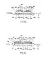
- FIGS. 1A–1Cillustrate a semiconductor package 100 constructed in accordance with a first embodiment of the present invention.
- the semiconductor package 100comprises a leadframe L/F (shown in FIG. 4A ) which itself includes a die paddle 110 having a generally quadrangular (e.g., square, rectangular) configuration.
- the die paddle 110defines a generally planar upper surface 110 a and an opposed, generally planar lower surface 110 b .
- the die paddle 110need not necessarily have a quadrangular shape, and may alternatively have a differing shape such as polygonal shape.
- the leadframe L/Fincludes a plurality of leads 120 which are arranged along the periphery of the die paddle 110 .
- the leads 120are preferably segregated into four sets, with the leads 120 of each set extending along and in spaced relation to a respective one of the four sides or peripheral edge segments of the die paddle 110 .
- the arrangement of the leads 120 as shown in FIG. 1Bis exemplary only, in that the leads 120 may alternatively be provided in two sets which extend along and in spaced relation to respective ones of two sides of the die paddle 110 .
- Other arrangements of the leads 120are also contemplated to be within the scope of the present invention.
- the leads 120 of each setare preferably spaced from each other at a constant pitch.
- the die paddle 110 and the leads 120will be fabricated from a conductive metal material such as copper, copper alloy, iron, or equivalents thereto. It is further contemplated that the die paddle 110 and leads 120 may be substituted in the semiconductor package 100 with a hard printed circuit board, a soft printed circuit board, a ceramic printed circuit board, or equivalents thereto.
- the semiconductor package 100 of the first embodimentfurther comprises a semiconductor die 140 which includes a generally planar upper surface 140 a and an opposed, generally planar lower surface 140 b .
- the lower surface 140 b of the semiconductor die 140is attached to the upper surface 110 a of the die paddle 110 . Such attachment is preferably facilitated through the use of an adhesive agent 130 such as an adhesive, adhesive film/tape, or epoxy.
- an adhesive agent 130such as an adhesive, adhesive film/tape, or epoxy.
- Disposed on the upper surface 140 a of the semiconductor die 140are a plurality of terminals or bond pads 141 .
- the bond pads 141are located in close proximity to the peripheral edge of the upper surface 140 a of the semiconductor die 140 .
- the location of the bond pads 141 along the outer periphery of the upper surface 140 ais to provide sufficient open area to accommodate one or more inner packages 160 of the semiconductor package 100 , as will be described in more detail below.
- the semiconductor package 100 of the first embodimentfurther comprises a plurality (e.g., four) inner packages 160 .
- Each inner package 160includes an inner die paddle 161 which itself preferably has a generally quadrangular (e.g., square, rectangular) configuration. Extending about the periphery of the die paddle 161 in spaced relation thereto is a plurality of inner leads 162 .
- the inner leads 162are also preferably segregated into four sets, with the inner leads 162 of each set extending along and in spaced relation to a respective one of the four sides or peripheral edge segments of the inner die paddle 161 .
- the inner leads 162 of each setare preferably spaced from each other at a constant pitch.
- Attached to the lower surface of the inner die paddle 161is an inner semiconductor die 163 .
- Conductive pads or terminals of the inner semiconductor die 163are electrically connected to respective ones of the inner leads 162 through the use of inner conductive wires 164 .
- the inner die paddle 161 , the inner leads 162 , the inner semiconductor die 163 , and the inner conductive wires 164 of each inner package 160are encapsulated by an encapsulant material which, upon hardening, forms an inner package body 165 of the inner package 160 .
- each inner package 160the fully formed inner package body 165 defines a generally planar upper surface 165 a .
- the inner die paddle 161defines a generally planar upper surface 161 a , which is that surface opposite that to which the semiconductor die 163 is attached.
- each of the inner leads 162defines a generally planar upper surface 162 a , which is that surface opposite that to which the inner conductive wires 164 are extended.
- the upper surface 161 a of the inner die paddle 161 and the upper surfaces 162 a of the inner leads 162are preferably exposed in and substantially flush with the upper surface 165 a of the inner package body 165 .
- the upper surfaces 161 a , 162 a , 165 aextend in generally co-planar relation to each other.
- the inner package body 165 of each inner package 160also defines a generally planar lower surface 165 b which is disposed in opposed relation to the upper surface 165 a thereof.
- the lower surface 165 b of the inner package body 165 of each inner package 160is preferably attached to the upper surface 140 a of the semiconductor die 140 through the use of an adhesive agent 150 .
- the semiconductor package 100 of the first embodimentis shown in FIGS. 1A–1C as including four inner packages 160 attached to the upper surface 140 a of the semiconductor die 140 in a generally square pattern.
- the number of inner packages 160 included in the semiconductor package 100is not limited to four as shown, but may include greater or fewer inner packages 160 .
- the present inventionis not intended to be limited to the above-described specific construction or configuration of each inner package 160 . That is, any type of inner packages having signal transfer nodes exposed through one or more surfaces of the package body thereof may be employed in the semiconductor package 100 of the present invention.
- any inner package incorporated into the semiconductor package 100may employ the use of a hard printed circuit board, a soft printed circuit board, or a ceramic printed circuit board, as an alternative to the above-described inner die paddle(s) 161 and inner leads 162 .
- the placement or positioning of the bond pads 141 of the semiconductor die 140 in close proximity to the peripheral edge of the upper surface 140 a thereofprovides a substantial open central area on the upper surface 140 a which is sufficient to accommodate the inner package(s) 160 .
- the semiconductor package 100 of the first embodimentfurther comprises a plurality of conductive wires 170 which are used to electrically connect at least some of the bond pads 141 of the semiconductor die 140 to respective leads 120 .
- a plurality of conductive wires 170which are used to electrically connect at least some of the bond pads 141 of the semiconductor die 140 to respective leads 120 .
- an electrical signal from the semiconductor die 140can be transferred through the conductive wires 170 and the leads 120 to an external device 190 (shown in FIG. 1C ), with an electrical signal from the external device 190 being able to be transferred to the semiconductor die 140 through an inverse path.
- the conductive wires 170may be gold wires, aluminum wires, copper wires, or equivalents thereto.
- the die paddle 110 , the leads 120 , the semiconductor die 140 , the inner package(s) 160 and the conductive wires 170are encapsulated with an encapsulant material which, upon hardening, forms a package body 180 of the semiconductor package 100 .
- the package body 180protects the components it covers from external dust and from moisture.
- the package body 180may be fabricated from epoxy, a plastic molding compound, ceramic, or equivalents thereto.
- at least some of the leads 120protrude from a side surface 180 c of the package body 180 , thereby allowing the semiconductor package 100 to be easily mounted to the external device 190 in the manner shown in FIG. 1C .
- those leads 120 which protrude from the side surface 180 c of the package body 180are preferably bent to impart a gull-wing configuration thereto.
- the fully formed package body 180 of the semiconductor package 100defines a generally planar upper surface 180 a .
- the package body 180 of the semiconductor package 100is formed such that the upper surface 161 a of the inner die paddle 161 , the upper surfaces 162 a of the inner leads 162 , and the upper surface 165 a of the inner package body 165 of each inner package 160 are exposed in and substantially flush with the upper surface 180 a of the package body 180 .
- the upper surfaces 161 a , 162 a , 165 a , 180 aextend in generally co-planar relation to each other.
- the leads 120 of the semiconductor package 100may be electrically connected to corresponding pads of the external device 190 , but the inner die paddle 161 and the inner leads 162 of each inner package 160 of the semiconductor package 100 may be electrically connected to corresponding pads on the external device 190 as well. Any such electrical connection between the semiconductor package 100 and the external device 190 is preferably accomplished through the use of layers of solder 191 . It should be noted that there is no electrical connection in the semiconductor package 100 between the inner package(s) 160 and the semiconductor die 140 or between the inner package(s) 160 and the leads 120 . However, these components may optionally be electrically connected to each other through the external device 190 .
- an electrical signal from the semiconductor die 140is transferred through the conductive wires 170 and the leads 120 to the external device 190 , with an electrical signal from the inner semiconductor die 163 of each inner package 160 being transferred through corresponding inner conductive wires 164 and corresponding inner leads 162 to the external device 190 .
- the semiconductor package 100is flipped over or inverted to facilitate its connection to the external device 190 , thus causing certain ones of those surfaces referred to above as “upper surfaces” to be directly adjacent the surface of the external device 190 to which the semiconductor device 100 is mounted.
- FIGS. 4A–4Ethere is shown an exemplary sequence of steps which may be used to facilitate the fabrication of the semiconductor package 100 of the first embodiment.
- the leadframe L/Fis provided, such leadframe L/F including the die paddle 110 and leads 120 have the above-described structural attributes and special relationships relative to each other ( FIG. 4A ).
- the semiconductor die 140is attached to the upper surface 110 a of the die paddle 110 through the use of the adhesive agent 130 ( FIG. 4B ).
- the inner package(s) 160 having the above-described structural attributesare then attached to the upper surface 140 a of the semiconductor die 140 in the aforementioned manner through the use of the adhesive agent 150 ( FIG. 4C ).
- the inner package(s) 160are attached to the semiconductor die 140 at positions which do not cause the same to overlap any of the bond pads 141 , such bond pads 141 also not being contaminated by the adhesive agent 150 .
- a wire bonding stepis completed wherein the bond pads 141 of the semiconductor die 140 are electrically connected to the leads 120 through the use of the conductive wires 170 ( FIG. 4D ).
- the package body 180is formed to have the above-described structural attributes ( FIG. 4E ), portions of the inner package(s) 160 being exposed in the upper surface 180 a of the package body 180 in the aforementioned manner.
- the semiconductor package 100 produced as a result of the completion of this fabrication methodologyincludes on or more inner packages 160 which are packaged in the single semiconductor package 100 , thus maximizing package density.
- the semiconductor package 100Since the inner die paddle 161 and the inner leads 160 of the inner package(s) 160 are exposed in the package body 180 , the semiconductor package 100 has a considerably reduced thickness, though possessing substantially increased signal transfer capability. Those of ordinary skill in the art will recognize that the construction of the semiconductor package 100 is not necessarily limited to the precise order or sequence of steps described above. For example, the electrical connection of the semiconductor die 140 to the leads 120 through the use of the conductive wires 170 may occur prior to the attachment of the inner package(s) 160 to the semiconductor die 140 .
- FIGS. 2A and 2Bthere is shown a semiconductor package 200 constructed in accordance with a second embodiment of the present invention.
- the semiconductor package 200 of the second embodimentbears substantial similarity in construction to the semiconductor package 100 of the first embodiment, with the 200 series reference numerals in FIGS. 2A and 2B being used to identify the same structures identified by the corresponding 100 series reference numerals included in FIGS. 1A–1C .
- the distinctions between the semiconductor packages 200 , 100will be discussed below.
- conductive wires 270are used to electrically connect at least some of the bond pads 241 of the semiconductor die 240 to respective leads 220 .
- the semiconductor package 200 of the second embodimentalso includes conductive wires 281 , 282 , and 283 which, like the conductive wires 270 , are covered by the package body 280 of the semiconductor package 200 .
- the conductive wires 281 , 282 , 283are used to establish electrical interconnection between the inner package(s) 260 and the semiconductor die 240 , between the inner package(s) 260 and the leads 220 , or between the inner packages 260 themselves. As shown in FIGS.
- the conductive wires 281electrically connect at least some of the inner leads 262 of the inner packages 260 to respective bond pads 241 of the semiconductor die 240 .
- the conductive wires 282electrically connect at least some of the inner leads 262 of the inner packages 260 to respective leads 220 .
- the conductive wires 283electrically connect at least some of the inner leads 262 of one inner package 260 to respective inner leads 262 of another inner package 260 .
- the length of the wires for grounding or power transfercan be reduced to reduce loss of electrical signal in the wires, with the additional absence of distortion of the grounding ring or power supply improving the reliability of the semiconductor package 200 .
- the package body 280 of the semiconductor package 200completely covers the die paddle 210 , semiconductor die 240 , inner packages 260 , and conductive wires 270 , 281 , 282 , 283 .
- no portion of any inner package 260is exposed in the package body 280 of the semiconductor package 200 .
- FIGS. 5A–5Ethere is shown an exemplary sequence of steps which may be used to facilitate the fabrication of the semiconductor package 200 of the second embodiment.
- the leadframe L/Fis provided, such leadframe L/F including the die paddle 210 and leads 220 ( FIG. 5A ).
- the semiconductor die 240is attached to the upper surface 210 a of the die paddle 210 through the use of the adhesive agent 230 ( FIG. 5B ).
- the inner package(s) 260are then attached to the upper surface 240 a of the semiconductor die 240 through the use of the adhesive agent 250 ( FIG. 5C ).
- a wire bonding stepis completed wherein the conductive wires 270 , 281 , 282 , 283 are used to establish electrical interconnections between the various components of the semiconductor package 200 in the above-described manner ( FIG. 5D ).
- the package body 280is formed the above-described structural attributes ( FIG. 5E ), the inner package(s) 260 being completely covered by the package body 280 .
- FIGS. 3A and 3Bthere is shown a semiconductor package 300 constructed in accordance with a third embodiment of the present invention.
- the semiconductor package 300 of the third embodimentbears substantial similarity in construction to the semiconductor package 200 of the first embodiment, with the 300 series reference numerals in FIGS. 3A and 3B being used to identify the same structures identified by the corresponding 200 series reference numerals included in FIGS. 2A and 2B , and the corresponding 100 series reference numerals included in FIGS. 1A–1C . Only the distinctions between the semiconductor packages 300 , 200 will be discussed below.
- the semiconductor packages 200 , 300lies in the structural attributes of the inner package(s) 360 of the semiconductor package 300 in comparison to those of the inner package(s) 260 of the semiconductor package 200 . More particularly, in each inner package 360 of the semiconductor package 300 , the inner die paddle 361 defines a generally planar lower surface 361 b which is disposed in opposed relation to the generally planar upper surface 361 a thereof. Similarly, each inner lead 362 defines a generally planar lower surface 362 b which is disposed in opposed relation to the generally planar upper surface 362 a thereof. The inner package body 365 itself defines a generally planar lower surface 365 b which is disposed in opposed relation to the generally planar upper surface 365 a thereof.
- the inner package body 365is formed such that the lower surface 361 b of the inner die paddle 361 and the lower surfaces 362 b of the inner leads 362 are exposed in and substantially flush with the lower surface 365 b of the inner package body 365 .
- the lower surfaces 361 b , 362 b , 365 bextend in generally co-planar relation to each other.
- each inner package 360is formed such that portions of each inner lead 362 protrude from a side surface 365 c of the inner package body 365 .
- portions of the upper surfaces 362 a of each of the inner leads 362are not covered by the inner package body 365 , and thus are exposed.
- the exposed upper surfaces 161 a , 162 a , 165 a , 261 a , 262 a , 265 aare disposed furthest from the upper surface 140 a , 240 a of the semiconductor die 140 , 240 , in the semiconductor package 300 , the exposed lower surfaces 361 b , 362 b , 365 b of each inner package 360 are attached to the upper surface 340 a of the semiconductor die 340 through the use of the adhesive agent 350 .
- the conductive wires 381are used to electrically connect the exposed portions of the upper surfaces 362 a of at least some of the inner leads 362 to respective bond pads 341 of the semiconductor die 340 , with the conductive wires 382 being used to electrically connect the exposed portions of the upper surfaces 362 a of at least some of the inner leads 362 to respective leads 320 .
- the conductive wires 383are used to electrically connect the exposed portions of the upper surfaces 362 a of at least some of the inner leads 362 of one inner package 360 to the exposed portions of the upper surfaces 362 a of respective inner leads 362 of another inner package 360 .
- the conductive wires 370are used to electrically connect at least some of the bond pads 341 of the semiconductor die 340 to respective leads 320 .
- the inner leads 362 of each inner package 360may be used for either grounding or power supply.
- the semiconductor package 300it is not necessary to interpose a grounding ring or power supply ring between the die paddle 310 and the leads 320 .
- the length of the wires for grounding or power transfercan be reduced, thus imparting improved reliability to the semiconductor package 300 .
- the conductive wires 370 , 381 , 382 , 383 of the semiconductor package 300are contemplated to be configured so as to not extend higher than the level of the upper surface 365 a of each inner package body 365 , thus allowing the semiconductor package 300 to have a reduced thickness.
- FIGS. 6A–6Ethere is shown an exemplary sequence of steps which may be used to facilitate the fabrication of the semiconductor package 300 of the third embodiment.
- the leadframe L/Fis provided, such leadframe L/F including the die paddle 310 and leads 320 ( FIG. 6A ).
- the semiconductor die 340is attached to the upper surface 310 a of the die paddle 310 through the use of the adhesive agent 330 ( FIG. 6B ).
- the inner package(s) 360 having the above-described structural attributesare then attached to the upper surface 340 a of the semiconductor die 340 in the aforementioned manner through the use of the adhesive agent 350 ( FIG. 6C ).
- a wire bonding stepis completed wherein the conductive wires 370 , 381 , 382 , 383 are used to electrically interconnect various components of the semiconductor package 300 to each other in the above-described manner ( FIG. 6D ).
- the package body 380is formed to have the above-described structural attributes ( FIG. 6E ).
Landscapes
- Physics & Mathematics (AREA)
- Condensed Matter Physics & Semiconductors (AREA)
- General Physics & Mathematics (AREA)
- Engineering & Computer Science (AREA)
- Computer Hardware Design (AREA)
- Microelectronics & Electronic Packaging (AREA)
- Power Engineering (AREA)
- Lead Frames For Integrated Circuits (AREA)
Abstract
Description
Claims (19)
Priority Applications (1)
| Application Number | Priority Date | Filing Date | Title |
|---|---|---|---|
| US10/921,642US7202554B1 (en) | 2004-08-19 | 2004-08-19 | Semiconductor package and its manufacturing method |
Applications Claiming Priority (1)
| Application Number | Priority Date | Filing Date | Title |
|---|---|---|---|
| US10/921,642US7202554B1 (en) | 2004-08-19 | 2004-08-19 | Semiconductor package and its manufacturing method |
Publications (1)
| Publication Number | Publication Date |
|---|---|
| US7202554B1true US7202554B1 (en) | 2007-04-10 |
Family
ID=37904207
Family Applications (1)
| Application Number | Title | Priority Date | Filing Date |
|---|---|---|---|
| US10/921,642Expired - LifetimeUS7202554B1 (en) | 2004-08-19 | 2004-08-19 | Semiconductor package and its manufacturing method |
Country Status (1)
| Country | Link |
|---|---|
| US (1) | US7202554B1 (en) |
Cited By (20)
| Publication number | Priority date | Publication date | Assignee | Title |
|---|---|---|---|---|
| US20080029905A1 (en)* | 2006-08-04 | 2008-02-07 | Stats Chippac Ltd. | Integrated circuit package-in-package system |
| US20080036051A1 (en)* | 2006-08-08 | 2008-02-14 | Espiritu Emmanuel A | Quad flat package |
| US20080150088A1 (en)* | 2006-12-20 | 2008-06-26 | Reed Paul A | Method for incorporating existing silicon die into 3d integrated stack |
| US20090079096A1 (en)* | 2007-09-20 | 2009-03-26 | Lionel Chien Tay | Integrated circuit package system with multiple device units |
| US20090085181A1 (en)* | 2007-09-28 | 2009-04-02 | Advincula Jr Abelardo Hadap | Integrated circuit package system with multiple die |
| US20100001384A1 (en)* | 2008-07-01 | 2010-01-07 | Henry Descalzo Bathan | Integrated circuit package system with lead-frame paddle scheme for single axis partial saw isolation |
| US20100025834A1 (en)* | 2008-08-01 | 2010-02-04 | Zigmund Ramirez Camacho | Fan-in interposer on lead frame for an integrated circuit package on package system |
| US20100078784A1 (en)* | 2008-09-30 | 2010-04-01 | Infineon Technologies Ag | Device including a power semiconductor chip |
| US20100140763A1 (en)* | 2008-12-04 | 2010-06-10 | Zigmund Ramirez Camacho | Integrated circuit packaging system with stacked paddle and method of manufacture thereof |
| US7745918B1 (en) | 2004-11-24 | 2010-06-29 | Amkor Technology, Inc. | Package in package (PiP) |
| US20110068447A1 (en)* | 2009-09-18 | 2011-03-24 | Zigmund Ramirez Camacho | Integrated circuit packaging system with circuitry stacking and method of manufacture thereof |
| US7982298B1 (en) | 2008-12-03 | 2011-07-19 | Amkor Technology, Inc. | Package in package semiconductor device |
| US8058715B1 (en) | 2009-01-09 | 2011-11-15 | Amkor Technology, Inc. | Package in package device for RF transceiver module |
| US8487420B1 (en) | 2008-12-08 | 2013-07-16 | Amkor Technology, Inc. | Package in package semiconductor device with film over wire |
| US9184148B2 (en) | 2013-10-24 | 2015-11-10 | Amkor Technology, Inc. | Semiconductor package and method therefor |
| US9184118B2 (en) | 2013-05-02 | 2015-11-10 | Amkor Technology Inc. | Micro lead frame structure having reinforcing portions and method |
| US9673122B2 (en) | 2014-05-02 | 2017-06-06 | Amkor Technology, Inc. | Micro lead frame structure having reinforcing portions and method |
| US9704725B1 (en) | 2012-03-06 | 2017-07-11 | Amkor Technology, Inc. | Semiconductor device with leadframe configured to facilitate reduced burr formation |
| US10811341B2 (en) | 2009-01-05 | 2020-10-20 | Amkor Technology Singapore Holding Pte Ltd. | Semiconductor device with through-mold via |
| US10932366B2 (en)* | 2013-02-01 | 2021-02-23 | Apple Inc. | Low profile packaging and assembly of a power conversion system in modular form |
Citations (337)
| Publication number | Priority date | Publication date | Assignee | Title |
|---|---|---|---|---|
| US2596993A (en) | 1949-01-13 | 1952-05-20 | United Shoe Machinery Corp | Method and mold for covering of eyelets by plastic injection |
| US3435815A (en) | 1966-07-15 | 1969-04-01 | Micro Tech Mfg Inc | Wafer dicer |
| US3734660A (en) | 1970-01-09 | 1973-05-22 | Tuthill Pump Co | Apparatus for fabricating a bearing device |
| US3838984A (en) | 1973-04-16 | 1974-10-01 | Sperry Rand Corp | Flexible carrier and interconnect for uncased ic chips |
| US4054238A (en) | 1976-03-23 | 1977-10-18 | Western Electric Company, Inc. | Method, apparatus and lead frame for assembling leads with terminals on a substrate |
| US4189342A (en) | 1971-10-07 | 1980-02-19 | U.S. Philips Corporation | Semiconductor device comprising projecting contact layers |
| JPS55163868A (en) | 1979-06-08 | 1980-12-20 | Fujitsu Ltd | Lead frame and semiconductor device using the same |
| US4258381A (en) | 1977-12-07 | 1981-03-24 | Steag, Kernergie Gmbh | Lead frame for a semiconductor device suitable for mass production |
| US4289922A (en) | 1979-09-04 | 1981-09-15 | Plessey Incorporated | Integrated circuit package and lead frame |
| US4301464A (en) | 1978-08-02 | 1981-11-17 | Hitachi, Ltd. | Lead frame and semiconductor device employing the same with improved arrangement of supporting leads for securing the semiconductor supporting member |
| US4332537A (en) | 1978-07-17 | 1982-06-01 | Dusan Slepcevic | Encapsulation mold with removable cavity plates |
| JPS58160095A (en) | 1982-03-12 | 1983-09-22 | 明産株式会社 | Slitter device automatically positioning slitter knife |
| US4417266A (en) | 1981-08-14 | 1983-11-22 | Amp Incorporated | Power and ground plane structure for chip carrier |
| US4451224A (en) | 1982-03-25 | 1984-05-29 | General Electric Company | Mold device for making plastic articles from resin |
| JPS59208756A (en) | 1983-05-12 | 1984-11-27 | Sony Corp | Manufacture of semiconductor device package |
| JPS59227143A (en) | 1983-06-07 | 1984-12-20 | Dainippon Printing Co Ltd | Package of integrated circuit |
| JPS6010756Y2 (en) | 1979-06-13 | 1985-04-11 | アイダエンジニアリング株式会社 | Roll feed device |
| US4530152A (en) | 1982-04-01 | 1985-07-23 | Compagnie Industrielle Des Telecommunications Cit-Alcatel | Method for encapsulating semiconductor components using temporary substrates |
| JPS60116239U (en) | 1984-01-12 | 1985-08-06 | 日産自動車株式会社 | Power MOSFET mounting structure |
| US4541003A (en) | 1978-12-27 | 1985-09-10 | Hitachi, Ltd. | Semiconductor device including an alpha-particle shield |
| JPS60231349A (en) | 1984-05-01 | 1985-11-16 | Toshiba Corp | lead frame |
| JPS60195957U (en) | 1984-06-06 | 1985-12-27 | スズキ株式会社 | Engine intake air temperature automatic adjustment device |
| US4646710A (en) | 1982-09-22 | 1987-03-03 | Crystal Systems, Inc. | Multi-wafer slicing with a fixed abrasive |
| EP0098968B1 (en) | 1982-07-13 | 1987-06-03 | AlliedSignal Inc. | Two piece casting wheel |
| US4707724A (en) | 1984-06-04 | 1987-11-17 | Hitachi, Ltd. | Semiconductor device and method of manufacturing thereof |
| US4727633A (en) | 1985-08-08 | 1988-03-01 | Tektronix, Inc. | Method of securing metallic members together |
| US4737839A (en) | 1984-03-19 | 1988-04-12 | Trilogy Computer Development Partners, Ltd. | Semiconductor chip mounting system |
| US4756080A (en) | 1986-01-27 | 1988-07-12 | American Microsystems, Inc. | Metal foil semiconductor interconnection method |
| JPS63205935A (en) | 1987-02-23 | 1988-08-25 | Toshiba Corp | Resin-encapsulated semiconductor device with heat sink |
| JPS63233555A (en) | 1987-03-23 | 1988-09-29 | Toshiba Corp | Resin-encapsulated semiconductor device |
| JPS63249345A (en) | 1987-04-06 | 1988-10-17 | Olympus Optical Co Ltd | Flexible mounting substrate |
| JPS63289951A (en) | 1987-05-22 | 1988-11-28 | Dainippon Printing Co Ltd | Lead frame |
| JPS63188964U (en) | 1987-05-28 | 1988-12-05 | ||
| JPS63316470A (en) | 1987-06-19 | 1988-12-23 | Alps Electric Co Ltd | Manufacture of thin film transistor |
| JPS6367762B2 (en) | 1981-07-23 | 1988-12-27 | Mazda Motor | |
| US4812896A (en) | 1986-11-13 | 1989-03-14 | Olin Corporation | Metal electronic package sealed with thermoplastic having a grafted metal deactivator and antioxidant |
| JPS6454749U (en) | 1987-09-30 | 1989-04-04 | ||
| US4862246A (en) | 1984-09-26 | 1989-08-29 | Hitachi, Ltd. | Semiconductor device lead frame with etched through holes |
| US4862245A (en) | 1985-04-18 | 1989-08-29 | International Business Machines Corporation | Package semiconductor chip |
| US4907067A (en) | 1988-05-11 | 1990-03-06 | Texas Instruments Incorporated | Thermally efficient power device package |
| US4920074A (en) | 1987-02-25 | 1990-04-24 | Hitachi, Ltd. | Surface mount plastic package semiconductor integrated circuit, manufacturing method thereof, as well as mounting method and mounted structure thereof |
| US4935803A (en) | 1988-09-09 | 1990-06-19 | Motorola, Inc. | Self-centering electrode for power devices |
| US4942454A (en) | 1987-08-05 | 1990-07-17 | Mitsubishi Denki Kabushiki Kaisha | Resin sealed semiconductor device |
| US4987475A (en) | 1988-02-29 | 1991-01-22 | Digital Equipment Corporation | Alignment of leads for ceramic integrated circuit packages |
| US5018003A (en) | 1988-10-20 | 1991-05-21 | Mitsubishi Denki Kabushiki Kaisha | Lead frame and semiconductor device |
| US5029386A (en) | 1990-09-17 | 1991-07-09 | Hewlett-Packard Company | Hierarchical tape automated bonding method |
| US5041902A (en) | 1989-12-14 | 1991-08-20 | Motorola, Inc. | Molded electronic package with compression structures |
| US5057900A (en) | 1988-10-17 | 1991-10-15 | Semiconductor Energy Laboratory Co., Ltd. | Electronic device and a manufacturing method for the same |
| US5059379A (en) | 1987-07-20 | 1991-10-22 | Mitsubishi Denki Kabushiki Kaisha | Method of resin sealing semiconductor devices |
| US5065223A (en) | 1989-05-31 | 1991-11-12 | Fujitsu Vlsi Limited | Packaged semiconductor device |
| US5070039A (en) | 1989-04-13 | 1991-12-03 | Texas Instruments Incorporated | Method of making an integrated circuit using a pre-served dam bar to reduce mold flash and to facilitate flash removal |
| US5087961A (en) | 1987-01-28 | 1992-02-11 | Lsi Logic Corporation | Semiconductor device package |
| US5091341A (en) | 1989-05-22 | 1992-02-25 | Kabushiki Kaisha Toshiba | Method of sealing semiconductor device with resin by pressing a lead frame to a heat sink using an upper mold pressure member |
| US5096852A (en) | 1988-06-02 | 1992-03-17 | Burr-Brown Corporation | Method of making plastic encapsulated multichip hybrid integrated circuits |
| US5118298A (en) | 1991-04-04 | 1992-06-02 | Advanced Interconnections Corporation | Through hole mounting of integrated circuit adapter leads |
| US5122860A (en) | 1987-08-26 | 1992-06-16 | Matsushita Electric Industrial Co., Ltd. | Integrated circuit device and manufacturing method thereof |
| US5134773A (en) | 1989-05-26 | 1992-08-04 | Gerard Lemaire | Method for making a credit card containing a microprocessor chip |
| US5151039A (en) | 1990-04-06 | 1992-09-29 | Advanced Interconnections Corporation | Integrated circuit adapter having gullwing-shaped leads |
| US5157475A (en) | 1988-07-08 | 1992-10-20 | Oki Electric Industry Co., Ltd. | Semiconductor device having a particular conductive lead structure |
| US5157480A (en) | 1991-02-06 | 1992-10-20 | Motorola, Inc. | Semiconductor device having dual electrical contact sites |
| US5168368A (en) | 1991-05-09 | 1992-12-01 | International Business Machines Corporation | Lead frame-chip package with improved configuration |
| US5172213A (en) | 1991-05-23 | 1992-12-15 | At&T Bell Laboratories | Molded circuit package having heat dissipating post |
| US5172214A (en) | 1991-02-06 | 1992-12-15 | Motorola, Inc. | Leadless semiconductor device and method for making the same |
| US5175060A (en) | 1989-07-01 | 1992-12-29 | Ibiden Co., Ltd. | Leadframe semiconductor-mounting substrate having a roughened adhesive conductor circuit substrate and method of producing the same |
| US5200809A (en) | 1991-09-27 | 1993-04-06 | Vlsi Technology, Inc. | Exposed die-attach heatsink package |
| US5200362A (en) | 1989-09-06 | 1993-04-06 | Motorola, Inc. | Method of attaching conductive traces to an encapsulated semiconductor die using a removable transfer film |
| US5214845A (en) | 1992-05-11 | 1993-06-01 | Micron Technology, Inc. | Method for producing high speed integrated circuits |
| US5216278A (en) | 1990-12-04 | 1993-06-01 | Motorola, Inc. | Semiconductor device having a pad array carrier package |
| US5218231A (en) | 1989-08-30 | 1993-06-08 | Kabushiki Kaisha Toshiba | Mold-type semiconductor device |
| US5221642A (en) | 1991-08-15 | 1993-06-22 | Staktek Corporation | Lead-on-chip integrated circuit fabrication method |
| US5250841A (en) | 1992-04-06 | 1993-10-05 | Motorola, Inc. | Semiconductor device with test-only leads |
| US5252853A (en) | 1991-09-19 | 1993-10-12 | Mitsubishi Denki Kabushiki Kaisha | Packaged semiconductor device having tab tape and particular power distribution lead structure |
| US5258094A (en) | 1991-09-18 | 1993-11-02 | Nec Corporation | Method for producing multilayer printed wiring boards |
| US5266834A (en) | 1989-03-13 | 1993-11-30 | Hitachi Ltd. | Semiconductor device and an electronic device with the semiconductor devices mounted thereon |
| US5277972A (en) | 1988-09-29 | 1994-01-11 | Tomoegawa Paper Co., Ltd. | Adhesive tapes |
| US5278446A (en) | 1992-07-06 | 1994-01-11 | Motorola, Inc. | Reduced stress plastic package |
| US5279029A (en) | 1990-08-01 | 1994-01-18 | Staktek Corporation | Ultra high density integrated circuit packages method |
| US5281849A (en) | 1991-05-07 | 1994-01-25 | Singh Deo Narendra N | Semiconductor package with segmented lead frame |
| US5294897A (en) | 1992-07-20 | 1994-03-15 | Mitsubishi Denki Kabushiki Kaisha | Microwave IC package |
| US5327008A (en) | 1993-03-22 | 1994-07-05 | Motorola Inc. | Semiconductor device having universal low-stress die support and method for making the same |
| US5332864A (en) | 1991-12-27 | 1994-07-26 | Vlsi Technology, Inc. | Integrated circuit package having an interposer |
| US5336931A (en) | 1993-09-03 | 1994-08-09 | Motorola, Inc. | Anchoring method for flow formed integrated circuit covers |
| US5335771A (en) | 1990-09-25 | 1994-08-09 | R. H. Murphy Company, Inc. | Spacer trays for stacking storage trays with integrated circuits |
| US5343076A (en) | 1990-07-21 | 1994-08-30 | Mitsui Petrochemical Industries, Ltd. | Semiconductor device with an airtight space formed internally within a hollow package |
| US5358905A (en) | 1993-04-02 | 1994-10-25 | Texas Instruments Incorporated | Semiconductor device having die pad locking to substantially reduce package cracking |
| US5365106A (en) | 1992-10-27 | 1994-11-15 | Kabushiki Kaisha Toshiba | Resin mold semiconductor device |
| US5381042A (en) | 1992-03-31 | 1995-01-10 | Amkor Electronics, Inc. | Packaged integrated circuit including heat slug having an exposed surface |
| EP0393997B1 (en) | 1989-04-20 | 1995-02-01 | Honeywell Inc. | Method of providing a variable-pitch leadframe assembly |
| US5391439A (en) | 1990-09-27 | 1995-02-21 | Dai Nippon Printing Co., Ltd. | Leadframe adapted to support semiconductor elements |
| US5406124A (en) | 1992-12-04 | 1995-04-11 | Mitsui Toatsu Chemicals, Inc. | Insulating adhesive tape, and lead frame and semiconductor device employing the tape |
| US5410180A (en) | 1992-07-28 | 1995-04-25 | Shinko Electric Industries Co., Ltd. | Metal plane support for multi-layer lead frames and a process for manufacturing such frames |
| US5414299A (en) | 1993-09-24 | 1995-05-09 | Vlsi Technology, Inc. | Semi-conductor device interconnect package assembly for improved package performance |
| US5417905A (en) | 1989-05-26 | 1995-05-23 | Esec (Far East) Limited | Method of making a card having decorations on both faces |
| US5428248A (en) | 1992-08-21 | 1995-06-27 | Goldstar Electron Co., Ltd. | Resin molded semiconductor package |
| US5435057A (en) | 1990-10-30 | 1995-07-25 | International Business Machines Corporation | Interconnection method and structure for organic circuit boards |
| US5444301A (en) | 1993-06-23 | 1995-08-22 | Goldstar Electron Co. Ltd. | Semiconductor package and method for manufacturing the same |
| US5452511A (en) | 1993-11-04 | 1995-09-26 | Chang; Alexander H. C. | Composite lead frame manufacturing method |
| US5454905A (en) | 1994-08-09 | 1995-10-03 | National Semiconductor Corporation | Method for manufacturing fine pitch lead frame |
| US5474958A (en) | 1993-05-04 | 1995-12-12 | Motorola, Inc. | Method for making semiconductor device having no die supporting surface |
| US5484274A (en) | 1992-11-24 | 1996-01-16 | Neu Dynamics Corp. | Encapsulation molding equipment |
| US5493151A (en) | 1993-07-15 | 1996-02-20 | Kabushiki Kaisha Toshiba | Semiconductor device, lead frame and method for manufacturing semiconductor devices |
| US5498902A (en)* | 1993-08-25 | 1996-03-12 | Seiko Epson Corporation | Semiconductor device and its manufacturing method |
| US5508556A (en) | 1994-09-02 | 1996-04-16 | Motorola, Inc. | Leaded semiconductor device having accessible power supply pad terminals |
| US5517056A (en) | 1993-09-30 | 1996-05-14 | Motorola, Inc. | Molded carrier ring leadframe having a particular resin injecting area design for gate removal and semiconductor device employing the same |
| US5521429A (en) | 1993-11-25 | 1996-05-28 | Sanyo Electric Co., Ltd. | Surface-mount flat package semiconductor device |
| US5528076A (en) | 1995-02-01 | 1996-06-18 | Motorola, Inc. | Leadframe having metal impregnated silicon carbide mounting area |
| US5530292A (en)* | 1990-03-15 | 1996-06-25 | Fujitsu Limited | Semiconductor device having a plurality of chips |
| US5534467A (en) | 1993-03-18 | 1996-07-09 | Lsi Logic Corporation | Semiconductor packages for high I/O semiconductor dies |
| US5539251A (en) | 1992-05-11 | 1996-07-23 | Micron Technology, Inc. | Tie bar over chip lead frame design |
| US5543657A (en) | 1994-10-07 | 1996-08-06 | International Business Machines Corporation | Single layer leadframe design with groundplane capability |
| US5544412A (en) | 1994-05-24 | 1996-08-13 | Motorola, Inc. | Method for coupling a power lead to a bond pad in an electronic module |
| US5545923A (en) | 1993-10-22 | 1996-08-13 | Lsi Logic Corporation | Semiconductor device assembly with minimized bond finger connections |
| US5581122A (en) | 1994-10-25 | 1996-12-03 | Industrial Technology Research Institute | Packaging assembly with consolidated common voltage connections for integrated circuits |
| US5592025A (en) | 1992-08-06 | 1997-01-07 | Motorola, Inc. | Pad array semiconductor device |
| US5592019A (en) | 1994-04-19 | 1997-01-07 | Mitsubishi Denki Kabushiki Kaisha | Semiconductor device and module |
| US5594274A (en) | 1993-07-01 | 1997-01-14 | Nec Corporation | Lead frame for use in a semiconductor device and method of manufacturing the semiconductor device using the same |
| US5595934A (en) | 1995-05-17 | 1997-01-21 | Samsung Electronics Co., Ltd. | Method for forming oxide protective film on bonding pads of semiconductor chips by UV/O3 treatment |
| US5604376A (en) | 1994-06-30 | 1997-02-18 | Digital Equipment Corporation | Paddleless molded plastic semiconductor chip package |
| US5608267A (en) | 1992-09-17 | 1997-03-04 | Olin Corporation | Molded plastic semiconductor package including heat spreader |
| US5608265A (en) | 1993-03-17 | 1997-03-04 | Hitachi, Ltd. | Encapsulated semiconductor device package having holes for electrically conductive material |
| US5625222A (en) | 1993-11-18 | 1997-04-29 | Fujitsu Limited | Semiconductor device in a resin package housed in a frame having high thermal conductivity |
| US5633528A (en) | 1994-05-25 | 1997-05-27 | Texas Instruments Incorporated | Lead frame structure for IC devices with strengthened encapsulation adhesion |
| US5640047A (en) | 1995-09-25 | 1997-06-17 | Mitsui High-Tec, Inc. | Ball grid assembly type semiconductor device having a heat diffusion function and an electric and magnetic shielding function |
| US5639990A (en) | 1992-06-05 | 1997-06-17 | Mitsui Toatsu Chemicals, Inc. | Solid printed substrate and electronic circuit package using the same |
| US5641997A (en) | 1993-09-14 | 1997-06-24 | Kabushiki Kaisha Toshiba | Plastic-encapsulated semiconductor device |
| US5643433A (en) | 1992-12-23 | 1997-07-01 | Shinko Electric Industries Co., Ltd. | Lead frame and method for manufacturing same |
| US5644169A (en) | 1993-03-04 | 1997-07-01 | Goldstar Electron Co., Ltd. | Mold and method for manufacturing a package for a semiconductor chip and the package manufactured thereby |
| US5646831A (en) | 1995-12-28 | 1997-07-08 | Vlsi Technology, Inc. | Electrically enhanced power quad flat pack arrangement |
| US5650663A (en) | 1995-07-03 | 1997-07-22 | Olin Corporation | Electronic package with improved thermal properties |
| US5661088A (en) | 1996-01-11 | 1997-08-26 | Motorola, Inc. | Electronic component and method of packaging |
| US5665996A (en) | 1994-12-30 | 1997-09-09 | Siliconix Incorporated | Vertical power mosfet having thick metal layer to reduce distributed resistance |
| EP0794572A2 (en) | 1996-03-07 | 1997-09-10 | Matsushita Electronics Corporation | Electronic component, method for making the same, and lead frame and mold assembly for use therein |
| US5673479A (en) | 1993-12-20 | 1997-10-07 | Lsi Logic Corporation | Method for mounting a microelectronic circuit peripherally-leaded package including integral support member with spacer |
| US5683806A (en) | 1988-09-29 | 1997-11-04 | Tomoegawa Paper Co., Ltd. | Adhesive tapes |
| US5689135A (en) | 1995-12-19 | 1997-11-18 | Micron Technology, Inc. | Multi-chip device and method of fabrication employing leads over and under processes |
| US5696666A (en) | 1995-10-11 | 1997-12-09 | Motorola, Inc. | Low profile exposed die chip carrier package |
| US5701034A (en) | 1994-05-03 | 1997-12-23 | Amkor Electronics, Inc. | Packaged semiconductor die including heat sink with locking feature |
| US5703407A (en) | 1995-02-14 | 1997-12-30 | Kabushiki Kaisha Toshiba | Resin-sealed type semiconductor device |
| US5710064A (en) | 1994-08-16 | 1998-01-20 | Samsung Electronics Co., Ltd. | Method for manufacturing a semiconductor package |
| JPH1022447A (en) | 1996-06-28 | 1998-01-23 | Goto Seisakusho:Kk | Resin-sealed semiconductor device and method of manufacturing the same |
| US5724233A (en) | 1993-07-09 | 1998-03-03 | Fujitsu Limited | Semiconductor device having first and second semiconductor chips with a gap therebetween, a die stage in the gap and associated lead frames disposed in a package, the lead frames providing electrical connections from the chips to an exterior of the packag |
| US5723899A (en) | 1994-08-30 | 1998-03-03 | Amkor Electronics, Inc. | Semiconductor lead frame having connection bar and guide rings |
| US5726493A (en) | 1994-06-13 | 1998-03-10 | Fujitsu Limited | Semiconductor device and semiconductor device unit having ball-grid-array type package structure |
| US5736432A (en) | 1996-09-20 | 1998-04-07 | National Semiconductor Corporation | Lead frame with lead finger locking feature and method for making same |
| US5745984A (en) | 1995-07-10 | 1998-05-05 | Martin Marietta Corporation | Method for making an electronic module |
| US5753532A (en) | 1995-08-30 | 1998-05-19 | Samsung Electronics Co., Ltd. | Method of manufacturing semiconductor chip package |
| US5753977A (en) | 1996-03-22 | 1998-05-19 | Mitsubishi Denki Kabushiki Kaisha | Semiconductor device and lead frame therefor |
| EP0844665A2 (en) | 1996-11-21 | 1998-05-27 | Texas Instruments Incorporated | Wafer level packaging |
| US5766972A (en) | 1994-06-02 | 1998-06-16 | Mitsubishi Denki Kabushiki Kaisha | Method of making resin encapsulated semiconductor device with bump electrodes |
| JPH10163401A (en) | 1996-12-04 | 1998-06-19 | Sony Corp | Lead frame, semiconductor package, and manufacture of semiconductor package |
| US5770888A (en) | 1995-12-29 | 1998-06-23 | Lg Semicon Co., Ltd. | Integrated chip package with reduced dimensions and leads exposed from the top and bottom of the package |
| US5776798A (en) | 1996-09-04 | 1998-07-07 | Motorola, Inc. | Semiconductor package and method thereof |
| DE19734794A1 (en) | 1997-01-09 | 1998-07-16 | Mitsubishi Electric Corp | Wiring part and lead frame with the wiring part |
| US5783861A (en) | 1994-03-29 | 1998-07-21 | Lg Semicon Co., Ltd. | Semiconductor package and lead frame |
| JPH10199934A (en) | 1997-01-13 | 1998-07-31 | Hitachi Ltd | Semiconductor element mounting structure and semiconductor element mounting method |
| US5801440A (en) | 1995-10-10 | 1998-09-01 | Acc Microelectronics Corporation | Chip package board having utility rings |
| JPH10256240A (en) | 1997-01-10 | 1998-09-25 | Sony Corp | Manufacture of semiconductor device |
| US5814884A (en) | 1996-10-24 | 1998-09-29 | International Rectifier Corporation | Commonly housed diverse semiconductor die |
| US5814881A (en) | 1996-12-20 | 1998-09-29 | Lsi Logic Corporation | Stacked integrated chip package and method of making same |
| US5814883A (en) | 1995-10-04 | 1998-09-29 | Mitsubishi Denki Kabushiki Kaisha | Packaged semiconductor chip |
| US5818105A (en) | 1994-07-22 | 1998-10-06 | Nec Corporation | Semiconductor device with plastic material covering a semiconductor chip mounted on a substrate of the device |
| US5817540A (en) | 1996-09-20 | 1998-10-06 | Micron Technology, Inc. | Method of fabricating flip-chip on leads devices and resulting assemblies |
| US5821615A (en) | 1995-12-06 | 1998-10-13 | Lg Semicon Co., Ltd. | Semiconductor chip package having clip-type outlead and fabrication method of same |
| US5821457A (en) | 1994-03-11 | 1998-10-13 | The Panda Project | Semiconductor die carrier having a dielectric epoxy between adjacent leads |
| US5834830A (en) | 1995-12-18 | 1998-11-10 | Lg Semicon Co., Ltd. | LOC (lead on chip) package and fabricating method thereof |
| US5835988A (en) | 1996-03-27 | 1998-11-10 | Mitsubishi Denki Kabushiki Kaisha | Packed semiconductor device with wrap around external leads |
| US5844306A (en) | 1995-09-28 | 1998-12-01 | Mitsubishi Denki Kabushiki Kaisha | Die pad structure for solder bonding |
| US5856911A (en) | 1996-11-12 | 1999-01-05 | National Semiconductor Corporation | Attachment assembly for integrated circuits |
| US5859471A (en) | 1992-11-17 | 1999-01-12 | Shinko Electric Industries Co., Ltd. | Semiconductor device having tab tape lead frame with reinforced outer leads |
| US5866939A (en) | 1996-01-21 | 1999-02-02 | Anam Semiconductor Inc. | Lead end grid array semiconductor package |
| US5871782A (en) | 1995-12-30 | 1999-02-16 | Lg Semicon Co. Ltd. | Transfer molding apparatus having laminated chase block |
| US5874784A (en) | 1995-10-25 | 1999-02-23 | Sharp Kabushiki Kaisha | Semiconductor device having external connection terminals provided on an interconnection plate and fabrication process therefor |
| US5877043A (en) | 1996-02-01 | 1999-03-02 | International Business Machines Corporation | Electronic package with strain relief means and method of making |
| US5886397A (en) | 1996-09-05 | 1999-03-23 | International Rectifier Corporation | Crushable bead on lead finger side surface to improve moldability |
| US5886398A (en) | 1997-09-26 | 1999-03-23 | Lsi Logic Corporation | Molded laminate package with integral mold gate |
| US5894108A (en) | 1997-02-11 | 1999-04-13 | National Semiconductor Corporation | Plastic package with exposed die |
| US5897339A (en) | 1996-09-11 | 1999-04-27 | Samsung Electronics Co., Ltd. | Lead-on-chip semiconductor device package having an adhesive layer formed from liquid adhesive and method for manufacturing the same |
| US5900676A (en) | 1996-08-19 | 1999-05-04 | Samsung Electronics Co., Ltd. | Semiconductor device package structure having column leads and a method for production thereof |
| US5903050A (en) | 1998-04-30 | 1999-05-11 | Lsi Logic Corporation | Semiconductor package having capacitive extension spokes and method for making the same |
| US5903049A (en) | 1997-10-29 | 1999-05-11 | Mitsubishi Denki Kabushiki Kaisha | Semiconductor module comprising semiconductor packages |
| US5917242A (en) | 1996-05-20 | 1999-06-29 | Micron Technology, Inc. | Combination of semiconductor interconnect |
| US5915998A (en) | 1996-06-19 | 1999-06-29 | Erico International Corporation | Electrical connector and method of making |
| US5939779A (en) | 1996-05-17 | 1999-08-17 | Lg Semicon Co., Ltd. | Bottom lead semiconductor chip stack package |
| US5942794A (en) | 1996-10-22 | 1999-08-24 | Matsushita Electronics Corporation | Plastic encapsulated semiconductor device and method of manufacturing the same |
| KR100220154B1 (en) | 1996-04-01 | 1999-09-01 | 김규현 | Method manufacture of semiconductor package |
| US5951305A (en) | 1998-07-09 | 1999-09-14 | Tessera, Inc. | Lidless socket and method of making same |
| US5959356A (en) | 1995-11-25 | 1999-09-28 | Samsung Electronics Co., Ltd. | Solder ball grid array carrier package with heat sink |
| US5969426A (en) | 1994-12-14 | 1999-10-19 | Mitsubishi Denki Kabushiki Kaisha | Substrateless resin encapsulated semiconductor device |
| US5973388A (en) | 1998-01-26 | 1999-10-26 | Motorola, Inc. | Leadframe, method of manufacturing a leadframe, and method of packaging an electronic component utilizing the leadframe |
| US5977615A (en) | 1996-12-24 | 1999-11-02 | Matsushita Electronics Corporation | Lead frame, method of manufacturing lead frame, semiconductor device and method of manufacturing semiconductor device |
| US5976912A (en) | 1994-03-18 | 1999-11-02 | Hitachi Chemical Company, Ltd. | Fabrication process of semiconductor package and semiconductor package |
| US5977630A (en) | 1997-08-15 | 1999-11-02 | International Rectifier Corp. | Plural semiconductor die housed in common package with split heat sink |
| WO1999056316A1 (en) | 1998-04-28 | 1999-11-04 | Tessera, Inc. | Encapsulation of microelectronic assemblies |
| US5981314A (en) | 1996-10-31 | 1999-11-09 | Amkor Technology, Inc. | Near chip size integrated circuit package |
| US5986333A (en) | 1997-02-27 | 1999-11-16 | Oki Electric Industry Co., Ltd. | Semiconductor apparatus and method for fabricating the same |
| US5986885A (en) | 1997-04-08 | 1999-11-16 | Integrated Device Technology, Inc. | Semiconductor package with internal heatsink and assembly method |
| US6001671A (en) | 1996-04-18 | 1999-12-14 | Tessera, Inc. | Methods for manufacturing a semiconductor package having a sacrificial layer |
| WO1999067821A1 (en) | 1998-06-24 | 1999-12-29 | Amkor Technology, Inc. | Plastic integrated circuit package and method and leadframe for making the package |
| US6013947A (en) | 1997-06-27 | 2000-01-11 | Trimecs Co., Ltd. | Substrate having gate recesses or slots and molding device and molding method thereof |
| US6018189A (en) | 1997-03-31 | 2000-01-25 | Nec Corporation | Lead frame for face-down bonding |
| US6020625A (en) | 1998-03-27 | 2000-02-01 | Mitsubishi Denki Kabushiki Kaisha | Lead frame including hanging leads and hanging lead reinforcement in a semiconductor device including the lead frame |
| US6025640A (en) | 1997-07-16 | 2000-02-15 | Dai Nippon Insatsu Kabushiki Kaisha | Resin-sealed semiconductor device, circuit member for use therein and method of manufacturing resin-sealed semiconductor device |
| US6031279A (en) | 1996-09-02 | 2000-02-29 | Siemens Aktiengesellschaft | Power semiconductor component |
| US6034423A (en) | 1998-04-02 | 2000-03-07 | National Semiconductor Corporation | Lead frame design for increased chip pinout |
| USRE36613E (en) | 1993-04-06 | 2000-03-14 | Micron Technology, Inc. | Multi-chip stacked devices |
| US6040626A (en) | 1998-09-25 | 2000-03-21 | International Rectifier Corp. | Semiconductor package |
| US6043430A (en) | 1997-03-14 | 2000-03-28 | Lg Semicon Co., Ltd. | Bottom lead semiconductor chip package |
| US6060768A (en) | 1995-05-09 | 2000-05-09 | Fujitsu Limited | Semiconductor device, method of manufacturing the semiconductor device, and method of manufacturing lead frame |
| US6072228A (en) | 1996-10-25 | 2000-06-06 | Micron Technology, Inc. | Multi-part lead frame with dissimilar materials and method of manufacturing |
| US6075284A (en) | 1998-06-30 | 2000-06-13 | Hyundai Electronics Industries Co., Ltd. | Stack package |
| US6081029A (en) | 1998-03-12 | 2000-06-27 | Matsushita Electronics Corporation | Resin encapsulated semiconductor device having a reduced thickness and improved reliability |
| US6084310A (en) | 1997-04-21 | 2000-07-04 | Nec Corporation | Semiconductor device, lead frame, and lead bonding |
| US6087722A (en) | 1998-05-28 | 2000-07-11 | Samsung Electronics Co., Ltd. | Multi-chip package |
| US6087715A (en) | 1997-04-22 | 2000-07-11 | Kabushiki Kaisha Toshiba | Semiconductor device, and manufacturing method of the same |
| US6100594A (en) | 1998-01-14 | 2000-08-08 | Sharp Kabushiki Kaisha | Semiconductor device and method of manufacturing the same |
| US6113473A (en) | 1997-04-25 | 2000-09-05 | G.T. Equipment Technologies Inc. | Method and apparatus for improved wire saw slurry |
| US6114752A (en) | 1998-11-10 | 2000-09-05 | Siliconware Precision Industries Co., Ltd. | Semiconductor package having lead frame with an exposed base pad |
| US6118174A (en) | 1996-12-28 | 2000-09-12 | Lg Semicon Co., Ltd. | Bottom lead frame and bottom lead semiconductor package using the same |
| US6118184A (en) | 1997-07-18 | 2000-09-12 | Sharp Kabushiki Kaisha | Semiconductor device sealed with a sealing resin and including structure to balance sealing resin flow |
| US6130473A (en) | 1998-04-02 | 2000-10-10 | National Semiconductor Corporation | Lead frame chip scale package |
| USRE36907E (en) | 1992-12-07 | 2000-10-10 | Integrated Device Technology, Inc. | Leadframe with power and ground planes |
| US6133623A (en) | 1996-07-03 | 2000-10-17 | Seiko Epson Corporation | Resin sealing type semiconductor device that includes a plurality of leads and method of making the same |
| US6169329B1 (en) | 1996-04-02 | 2001-01-02 | Micron Technology, Inc. | Semiconductor devices having interconnections using standardized bonding locations and methods of designing |
| US6177718B1 (en) | 1998-04-28 | 2001-01-23 | Kabushiki Kaisha Toshiba | Resin-sealed semiconductor device |
| US6181002B1 (en) | 1998-12-22 | 2001-01-30 | Sharp Kabushiki Kaisha | Semiconductor device having a plurality of semiconductor chips |
| US6184573B1 (en) | 1999-05-13 | 2001-02-06 | Siliconware Precision Industries Co., Ltd. | Chip packaging |
| US6184465B1 (en) | 1998-11-12 | 2001-02-06 | Micron Technology, Inc. | Semiconductor package |
| US6190944B1 (en)* | 1999-01-20 | 2001-02-20 | Hyundai Electronics Industries Co., Ltd. | Stacked package for semiconductor device and fabrication method thereof, and apparatus for making the stacked package |
| US6194777B1 (en) | 1998-06-27 | 2001-02-27 | Texas Instruments Incorporated | Leadframes with selective palladium plating |
| US6198171B1 (en) | 1999-12-30 | 2001-03-06 | Siliconware Precision Industries Co., Ltd. | Thermally enhanced quad flat non-lead package of semiconductor |
| US6197615B1 (en) | 1997-04-04 | 2001-03-06 | Samsung Electronics Co., Ltd. | Method of producing lead frame having uneven surfaces |
| JP2001060648A (en) | 1999-08-23 | 2001-03-06 | Dainippon Printing Co Ltd | Lead frame, method of manufacturing the same, and semiconductor device |
| US6201186B1 (en) | 1998-06-29 | 2001-03-13 | Motorola, Inc. | Electronic component assembly and method of making the same |
| US6201292B1 (en) | 1997-04-02 | 2001-03-13 | Dai Nippon Insatsu Kabushiki Kaisha | Resin-sealed semiconductor device, circuit member used therefor |
| US6204554B1 (en) | 1996-09-05 | 2001-03-20 | International Rectifier Corporation | Surface mount semiconductor package |
| US6208020B1 (en) | 1999-02-24 | 2001-03-27 | Matsushita Electronics Corporation | Leadframe for use in manufacturing a resin-molded semiconductor device |
| US6208023B1 (en) | 1997-07-31 | 2001-03-27 | Matsushita Electronics Corporation | Lead frame for use with an RF powered semiconductor |
| US6208021B1 (en) | 1996-03-27 | 2001-03-27 | Oki Electric Industry Co., Ltd. | Semiconductor device, manufacturing method thereof and aggregate type semiconductor device |
| US6211462B1 (en) | 1998-11-05 | 2001-04-03 | Texas Instruments Incorporated | Low inductance power package for integrated circuits |
| US6218731B1 (en) | 1999-05-21 | 2001-04-17 | Siliconware Precision Industries Co., Ltd. | Tiny ball grid array package |
| US6222259B1 (en) | 1998-09-15 | 2001-04-24 | Hyundai Electronics Industries Co., Ltd. | Stack package and method of fabricating the same |
| US6222258B1 (en) | 1996-11-11 | 2001-04-24 | Fujitsu Limited | Semiconductor device and method for producing a semiconductor device |
| US6229200B1 (en) | 1998-06-10 | 2001-05-08 | Asat Limited | Saw-singulated leadless plastic chip carrier |
| US6229205B1 (en) | 1997-06-30 | 2001-05-08 | Samsung Electronics Co., Ltd. | Semiconductor device package having twice-bent tie bar and small die pad |
| US6239384B1 (en) | 1995-09-18 | 2001-05-29 | Tessera, Inc. | Microelectric lead structures with plural conductors |
| US6239367B1 (en)* | 1999-01-29 | 2001-05-29 | United Microelectronics Corp. | Multi-chip chip scale package |
| US6239366B1 (en)* | 1999-01-28 | 2001-05-29 | United Microelectronics Corp. | Face-to-face multi-chip package |
| JP3177060B2 (en) | 1992-04-13 | 2001-06-18 | 株式会社リコー | Reversible thermosensitive recording label and card |
| US6256200B1 (en) | 1999-05-27 | 2001-07-03 | Allen K. Lam | Symmetrical package for semiconductor die |
| US6258629B1 (en) | 1999-08-09 | 2001-07-10 | Amkor Technology, Inc. | Electronic device package and leadframe and method for making the package |
| US20010008305A1 (en) | 1998-06-10 | 2001-07-19 | Asat Ltd. | Leadless plastic chip carrier with etch back pad singulation |
| EP0459493B1 (en) | 1990-06-01 | 2001-08-16 | Kabushiki Kaisha Toshiba | A semiconductor device comprising a TAB tape and its manufacturing method |
| US20010014538A1 (en) | 1998-06-10 | 2001-08-16 | Asat Ltd. | Leadless plastic chip carrier with etch back pad singulation and die attach pad array |
| US6281566B1 (en) | 1996-09-30 | 2001-08-28 | Sgs-Thomson Microelectronics S.R.L. | Plastic package for electronic devices |
| US6281568B1 (en) | 1998-10-21 | 2001-08-28 | Amkor Technology, Inc. | Plastic integrated circuit device package and leadframe having partially undercut leads and die pad |
| US6282095B1 (en) | 1999-02-02 | 2001-08-28 | Compaq Computer Corporation | Method and system for controlling radio frequency radiation in microelectronic packages using heat dissipation structures |
| US6285075B1 (en) | 1998-11-02 | 2001-09-04 | Asat, Limited | Integrated circuit package with bonding planes on a ceramic ring using an adhesive assembly |
| US6291273B1 (en) | 1996-12-26 | 2001-09-18 | Hitachi, Ltd. | Plastic molded type semiconductor device and fabrication process thereof |
| US6291271B1 (en) | 1999-09-14 | 2001-09-18 | Advanced Semiconductor Engineering, Inc. | Method of making semiconductor chip package |
| US6294100B1 (en) | 1998-06-10 | 2001-09-25 | Asat Ltd | Exposed die leadless plastic chip carrier |
| US6295977B1 (en) | 1998-11-05 | 2001-10-02 | Wacker Chemie Gmbh | Method and device for simultaneously cutting off a multiplicity of wafers from a workpiece |
| US6297548B1 (en) | 1998-06-30 | 2001-10-02 | Micron Technology, Inc. | Stackable ceramic FBGA for high thermal applications |
| US6303997B1 (en) | 1998-04-08 | 2001-10-16 | Anam Semiconductor, Inc. | Thin, stackable semiconductor packages |
| US6303981B1 (en)* | 1999-09-01 | 2001-10-16 | Micron Technology, Inc. | Semiconductor package having stacked dice and leadframes and method of fabrication |
| US6303984B1 (en) | 1997-08-12 | 2001-10-16 | Micron Technology, Inc. | Lead frame including angle iron tie bar |
| US6307272B1 (en) | 1998-05-27 | 2001-10-23 | Hitachi, Ltd. | Semiconductor device and method for manufacturing the same |
| US6309909B1 (en) | 1998-07-02 | 2001-10-30 | Mitsubishi Denki Kabushiki Kaisha | Semiconductor device and method of manufacturing the same |
| US6316838B1 (en) | 1999-10-29 | 2001-11-13 | Fujitsu Limited | Semiconductor device |
| US6316822B1 (en) | 1998-09-16 | 2001-11-13 | Texas Instruments Incorporated | Multichip assembly semiconductor |
| US6323550B1 (en) | 1995-06-06 | 2001-11-27 | Analog Devices, Inc. | Package for sealing an integrated circuit die |
| US6326243B1 (en) | 1995-08-15 | 2001-12-04 | Kabushiki Kaisha Toshiba | Resin sealed semiconductor device including a die pad uniformly having heat conducting paths and circulating holes for fluid resin |
| US6326678B1 (en) | 1993-09-03 | 2001-12-04 | Asat, Limited | Molded plastic package with heat sink and enhanced electrical performance |
| US6326244B1 (en) | 1998-09-03 | 2001-12-04 | Micron Technology, Inc. | Method of making a cavity ball grid array apparatus |
| US6335564B1 (en) | 1998-05-06 | 2002-01-01 | Conexant Systems, Inc. | Single Paddle having a semiconductor device and a passive electronic component |
| US6337510B1 (en) | 2000-11-17 | 2002-01-08 | Walsin Advanced Electronics Ltd | Stackable QFN semiconductor package |
| JP2002004397A (en) | 2000-06-23 | 2002-01-09 | Kubota Corp | Pipeline construction method |
| US6339255B1 (en) | 1998-10-24 | 2002-01-15 | Hyundai Electronics Industries Co., Ltd. | Stacked semiconductor chips in a single semiconductor package |
| US20020011654A1 (en) | 2000-07-25 | 2002-01-31 | Naoto Kimura | Semiconductor device |
| US6348726B1 (en) | 2001-01-18 | 2002-02-19 | National Semiconductor Corporation | Multi row leadless leadframe package |
| US20020024122A1 (en) | 2000-08-25 | 2002-02-28 | Samsung Electronics Co., Ltd. | Lead frame having a side ring pad and semiconductor chip package including the same |
| US20020027297A1 (en) | 2000-09-04 | 2002-03-07 | Chikao Ikenaga | Semiconductor package |
| US6355502B1 (en) | 2000-04-25 | 2002-03-12 | National Science Council | Semiconductor package and method for making the same |
| US6369454B1 (en) | 1998-12-31 | 2002-04-09 | Amkor Technology, Inc. | Semiconductor package and method for fabricating the same |
| US6369447B2 (en) | 1998-04-20 | 2002-04-09 | Mitsubishi Denki Kabushiki Kaisha | Plastic-packaged semiconductor device including a plurality of chips |
| US6373127B1 (en) | 1998-09-29 | 2002-04-16 | Texas Instruments Incorporated | Integrated capacitor on the back of a chip |
| US6380048B1 (en) | 2001-08-02 | 2002-04-30 | St Assembly Test Services Pte Ltd | Die paddle enhancement for exposed pad in semiconductor packaging |
| US6384472B1 (en) | 2000-03-24 | 2002-05-07 | Siliconware Precision Industries Co., Ltd | Leadless image sensor package structure and method for making the same |
| US6388336B1 (en) | 1999-09-15 | 2002-05-14 | Texas Instruments Incorporated | Multichip semiconductor assembly |
| US6395578B1 (en) | 1999-05-20 | 2002-05-28 | Amkor Technology, Inc. | Semiconductor package and method for fabricating the same |
| US6400004B1 (en) | 2000-08-17 | 2002-06-04 | Advanced Semiconductor Engineering, Inc. | Leadless semiconductor package |
| US6410979B2 (en) | 1998-12-21 | 2002-06-25 | Nec Corporation | Ball-grid-array semiconductor device with protruding terminals |
| US6414385B1 (en) | 1999-11-08 | 2002-07-02 | Siliconware Precisionindustries Co., Ltd. | Quad flat non-lead package of semiconductor |
| US6420779B1 (en) | 1999-09-14 | 2002-07-16 | St Assembly Test Services Ltd. | Leadframe based chip scale package and method of producing the same |
| US6429508B1 (en) | 2000-08-09 | 2002-08-06 | Kostat Semiconductor Co., Ltd. | Semiconductor package having implantable conductive lands and method for manufacturing the same |
| US20020105091A1 (en)* | 2001-02-06 | 2002-08-08 | Mitsubishi Denki Kabushiki Kaisha | Dual package semiconductor device |
| US6437429B1 (en) | 2001-05-11 | 2002-08-20 | Walsin Advanced Electronics Ltd | Semiconductor package with metal pads |
| US6444499B1 (en) | 2000-03-30 | 2002-09-03 | Amkor Technology, Inc. | Method for fabricating a snapable multi-package array substrate, snapable multi-package array and snapable packaged electronic components |
| US6448633B1 (en) | 1998-11-20 | 2002-09-10 | Amkor Technology, Inc. | Semiconductor package and method of making using leadframe having lead locks to secure leads to encapsulant |
| US6452279B2 (en) | 2000-07-14 | 2002-09-17 | Mitsubishi Denki Kabushiki Kaisha | Semiconductor device |
| US6459148B1 (en) | 2000-11-13 | 2002-10-01 | Walsin Advanced Electronics Ltd | QFN semiconductor package |
| US20020140068A1 (en) | 2001-03-28 | 2002-10-03 | Ming-Hsun Lee | Leadframe-based semiconductor package for multi-media card |
| US20020140061A1 (en) | 2001-03-27 | 2002-10-03 | Lee Hyung Ju | Lead frame for semiconductor package |
| US6464121B2 (en) | 2000-12-21 | 2002-10-15 | Xerox Corporation | Specialized tool adapted for a process for manufacture and interconnection between adjoining printed wiring boards |
| US6476469B2 (en) | 2000-11-23 | 2002-11-05 | Siliconware Precision Industries Co., Ltd. | Quad flat non-leaded package structure for housing CMOS sensor |
| US6476474B1 (en) | 2000-10-10 | 2002-11-05 | Siliconware Precision Industries Co., Ltd. | Dual-die package structure and method for fabricating the same |
| US20020163015A1 (en) | 2001-02-27 | 2002-11-07 | Chippac, Inc. | Plastic semiconductor package |
| US6482680B1 (en) | 2001-07-20 | 2002-11-19 | Carsem Semiconductor Sdn, Bhd. | Flip-chip on lead frame |
| US6498392B2 (en) | 2000-01-24 | 2002-12-24 | Nec Corporation | Semiconductor devices having different package sizes made by using common parts |
| US6498099B1 (en) | 1998-06-10 | 2002-12-24 | Asat Ltd. | Leadless plastic chip carrier with etch back pad singulation |
| US6507096B2 (en) | 2000-08-09 | 2003-01-14 | Kostat Semiconductor Co., Ltd. | Tape having implantable conductive lands for semiconductor packaging process and method for manufacturing the same |
| US6507120B2 (en) | 2000-12-22 | 2003-01-14 | Siliconware Precision Industries Co., Ltd. | Flip chip type quad flat non-leaded package |
| US6507098B1 (en)* | 1999-08-05 | 2003-01-14 | Siliconware Precision Industries Co., Ltd. | Multi-chip packaging structure |
| US20030030131A1 (en) | 2000-09-15 | 2003-02-13 | Samsung Techwin Co., Ltd., | Semiconductor package apparatus and method |
| US6534874B1 (en)* | 1999-11-02 | 2003-03-18 | Matsushita Electronics Corporation | Semiconductor device and method of producing the same |
| US6545345B1 (en) | 2001-03-20 | 2003-04-08 | Amkor Technology, Inc. | Mounting for a package containing a chip |
| US6545332B2 (en) | 2001-01-17 | 2003-04-08 | Siliconware Precision Industries Co., Ltd. | Image sensor of a quad flat package |
| US20030073265A1 (en) | 2001-10-12 | 2003-04-17 | Tom Hu | Semiconductor package with singulation crease |
| US6559525B2 (en) | 2000-01-13 | 2003-05-06 | Siliconware Precision Industries Co., Ltd. | Semiconductor package having heat sink at the outer surface |
| EP0936671B1 (en) | 1998-02-12 | 2003-05-07 | Hitachi, Ltd. | Resin-moulded semiconductor hybrid module and manufacturing method thereof |
| US6566760B1 (en)* | 1999-08-06 | 2003-05-20 | Hitachi, Ltd | Semiconductor storage device having memory chips in a stacked structure |
| US6583503B2 (en) | 1997-03-10 | 2003-06-24 | Micron Technology, Inc. | Semiconductor package with stacked substrates and multiple semiconductor dice |
| US6624005B1 (en) | 2000-09-06 | 2003-09-23 | Amkor Technology, Inc. | Semiconductor memory cards and method of making same |
| US6650006B2 (en)* | 2001-05-25 | 2003-11-18 | Siliconware Precision Industries Co., Ltd. | Semiconductor package with stacked chips |
| US6667546B2 (en) | 2001-11-15 | 2003-12-23 | Siliconware Precision Industries Co., Ltd. | Ball grid array semiconductor package and substrate without power ring or ground ring |
| US6690089B2 (en)* | 2002-05-15 | 2004-02-10 | Oki Electric Industry Co., Ltd. | Semiconductor device having multi-chip package |
| US20040056277A1 (en) | 2002-09-17 | 2004-03-25 | Chippac, Inc. | Semiconductor multi-package module including stacked-die package and having wire bond interconnect between stacked packages |
| US20040061212A1 (en) | 2002-09-17 | 2004-04-01 | Chippac, Inc. | Semiconductor multi-package module having wire bond interconnect between stacked packages |
| US20040061213A1 (en) | 2002-09-17 | 2004-04-01 | Chippac, Inc. | Semiconductor multi-package module having package stacked over die-up flip chip ball grid array package and having wire bond interconnect between stacked packages |
| US20040063242A1 (en) | 2002-09-17 | 2004-04-01 | Chippac, Inc. | Semiconductor multi-package module having package stacked over ball grid array package and having wire bond interconnect between stacked packages |
| US20040063246A1 (en) | 2002-09-17 | 2004-04-01 | Chippac, Inc. | Semiconductor multi-package module having package stacked over die-down flip chip ball grid array package and having wire bond interconnect between stacked packages |
| US20040065963A1 (en) | 2002-09-17 | 2004-04-08 | Chippac, Inc. | Semiconductor multi-package module having wire bond interconnect between stacked packages and having electrical shield |
| US6747361B2 (en)* | 2000-07-26 | 2004-06-08 | Nec Electronics Corporation | Semiconductor device and packaging method thereof |
| EP0720225B1 (en) | 1994-12-30 | 2004-10-27 | SILICONIX Incorporated | Lateral power MOSFET having metal strap layer to reduce distributed resistance and method of fabricating the same |
| US6841858B2 (en)* | 2002-09-27 | 2005-01-11 | St Assembly Test Services Pte Ltd. | Leadframe for die stacking applications and related die stacking concepts |
| US6861288B2 (en)* | 2003-01-23 | 2005-03-01 | St Assembly Test Services, Ltd. | Stacked semiconductor packages and method for the fabrication thereof |
| US6906424B2 (en)* | 2002-08-02 | 2005-06-14 | Micron Technology, Inc. | Semiconductor package and method producing same |
| US6905913B2 (en)* | 2000-03-17 | 2005-06-14 | Oki Electric Industry Co., Ltd. | Semiconductor device and method of manufacturing same |
- 2004
- 2004-08-19USUS10/921,642patent/US7202554B1/ennot_activeExpired - Lifetime
Patent Citations (356)
| Publication number | Priority date | Publication date | Assignee | Title |
|---|---|---|---|---|
| US2596993A (en) | 1949-01-13 | 1952-05-20 | United Shoe Machinery Corp | Method and mold for covering of eyelets by plastic injection |
| US3435815A (en) | 1966-07-15 | 1969-04-01 | Micro Tech Mfg Inc | Wafer dicer |
| US3734660A (en) | 1970-01-09 | 1973-05-22 | Tuthill Pump Co | Apparatus for fabricating a bearing device |
| US4189342A (en) | 1971-10-07 | 1980-02-19 | U.S. Philips Corporation | Semiconductor device comprising projecting contact layers |
| US3838984A (en) | 1973-04-16 | 1974-10-01 | Sperry Rand Corp | Flexible carrier and interconnect for uncased ic chips |
| US4054238A (en) | 1976-03-23 | 1977-10-18 | Western Electric Company, Inc. | Method, apparatus and lead frame for assembling leads with terminals on a substrate |
| US4258381A (en) | 1977-12-07 | 1981-03-24 | Steag, Kernergie Gmbh | Lead frame for a semiconductor device suitable for mass production |
| US4332537A (en) | 1978-07-17 | 1982-06-01 | Dusan Slepcevic | Encapsulation mold with removable cavity plates |
| US4301464A (en) | 1978-08-02 | 1981-11-17 | Hitachi, Ltd. | Lead frame and semiconductor device employing the same with improved arrangement of supporting leads for securing the semiconductor supporting member |
| US4541003A (en) | 1978-12-27 | 1985-09-10 | Hitachi, Ltd. | Semiconductor device including an alpha-particle shield |
| JPS55163868A (en) | 1979-06-08 | 1980-12-20 | Fujitsu Ltd | Lead frame and semiconductor device using the same |
| JPS6010756Y2 (en) | 1979-06-13 | 1985-04-11 | アイダエンジニアリング株式会社 | Roll feed device |
| US4289922A (en) | 1979-09-04 | 1981-09-15 | Plessey Incorporated | Integrated circuit package and lead frame |
| JPS6367762B2 (en) | 1981-07-23 | 1988-12-27 | Mazda Motor | |
| US4417266A (en) | 1981-08-14 | 1983-11-22 | Amp Incorporated | Power and ground plane structure for chip carrier |
| JPS58160095A (en) | 1982-03-12 | 1983-09-22 | 明産株式会社 | Slitter device automatically positioning slitter knife |
| US4451224A (en) | 1982-03-25 | 1984-05-29 | General Electric Company | Mold device for making plastic articles from resin |
| US4530152A (en) | 1982-04-01 | 1985-07-23 | Compagnie Industrielle Des Telecommunications Cit-Alcatel | Method for encapsulating semiconductor components using temporary substrates |
| EP0098968B1 (en) | 1982-07-13 | 1987-06-03 | AlliedSignal Inc. | Two piece casting wheel |
| US4646710A (en) | 1982-09-22 | 1987-03-03 | Crystal Systems, Inc. | Multi-wafer slicing with a fixed abrasive |
| JPS59208756A (en) | 1983-05-12 | 1984-11-27 | Sony Corp | Manufacture of semiconductor device package |
| JPS59227143A (en) | 1983-06-07 | 1984-12-20 | Dainippon Printing Co Ltd | Package of integrated circuit |
| JPS60116239U (en) | 1984-01-12 | 1985-08-06 | 日産自動車株式会社 | Power MOSFET mounting structure |
| US4737839A (en) | 1984-03-19 | 1988-04-12 | Trilogy Computer Development Partners, Ltd. | Semiconductor chip mounting system |
| JPS60231349A (en) | 1984-05-01 | 1985-11-16 | Toshiba Corp | lead frame |
| US4707724A (en) | 1984-06-04 | 1987-11-17 | Hitachi, Ltd. | Semiconductor device and method of manufacturing thereof |
| JPS60195957U (en) | 1984-06-06 | 1985-12-27 | スズキ株式会社 | Engine intake air temperature automatic adjustment device |
| US4862246A (en) | 1984-09-26 | 1989-08-29 | Hitachi, Ltd. | Semiconductor device lead frame with etched through holes |
| US4862245A (en) | 1985-04-18 | 1989-08-29 | International Business Machines Corporation | Package semiconductor chip |
| US4727633A (en) | 1985-08-08 | 1988-03-01 | Tektronix, Inc. | Method of securing metallic members together |
| US4756080A (en) | 1986-01-27 | 1988-07-12 | American Microsystems, Inc. | Metal foil semiconductor interconnection method |
| US4812896A (en) | 1986-11-13 | 1989-03-14 | Olin Corporation | Metal electronic package sealed with thermoplastic having a grafted metal deactivator and antioxidant |
| US5087961A (en) | 1987-01-28 | 1992-02-11 | Lsi Logic Corporation | Semiconductor device package |
| JPS63205935A (en) | 1987-02-23 | 1988-08-25 | Toshiba Corp | Resin-encapsulated semiconductor device with heat sink |
| US4920074A (en) | 1987-02-25 | 1990-04-24 | Hitachi, Ltd. | Surface mount plastic package semiconductor integrated circuit, manufacturing method thereof, as well as mounting method and mounted structure thereof |
| JPS63233555A (en) | 1987-03-23 | 1988-09-29 | Toshiba Corp | Resin-encapsulated semiconductor device |
| JPS63249345A (en) | 1987-04-06 | 1988-10-17 | Olympus Optical Co Ltd | Flexible mounting substrate |
| JPS63289951A (en) | 1987-05-22 | 1988-11-28 | Dainippon Printing Co Ltd | Lead frame |
| JPS63188964U (en) | 1987-05-28 | 1988-12-05 | ||
| JPS63316470A (en) | 1987-06-19 | 1988-12-23 | Alps Electric Co Ltd | Manufacture of thin film transistor |
| US5059379A (en) | 1987-07-20 | 1991-10-22 | Mitsubishi Denki Kabushiki Kaisha | Method of resin sealing semiconductor devices |
| US4942454A (en) | 1987-08-05 | 1990-07-17 | Mitsubishi Denki Kabushiki Kaisha | Resin sealed semiconductor device |
| US5122860A (en) | 1987-08-26 | 1992-06-16 | Matsushita Electric Industrial Co., Ltd. | Integrated circuit device and manufacturing method thereof |
| JPS6454749U (en) | 1987-09-30 | 1989-04-04 | ||
| US4987475A (en) | 1988-02-29 | 1991-01-22 | Digital Equipment Corporation | Alignment of leads for ceramic integrated circuit packages |
| US4907067A (en) | 1988-05-11 | 1990-03-06 | Texas Instruments Incorporated | Thermally efficient power device package |
| US5096852A (en) | 1988-06-02 | 1992-03-17 | Burr-Brown Corporation | Method of making plastic encapsulated multichip hybrid integrated circuits |
| US5157475A (en) | 1988-07-08 | 1992-10-20 | Oki Electric Industry Co., Ltd. | Semiconductor device having a particular conductive lead structure |
| US4935803A (en) | 1988-09-09 | 1990-06-19 | Motorola, Inc. | Self-centering electrode for power devices |
| US5277972A (en) | 1988-09-29 | 1994-01-11 | Tomoegawa Paper Co., Ltd. | Adhesive tapes |
| US5683806A (en) | 1988-09-29 | 1997-11-04 | Tomoegawa Paper Co., Ltd. | Adhesive tapes |
| US5277972B1 (en) | 1988-09-29 | 1996-11-05 | Tomoegawa Paper Co Ltd | Adhesive tapes |
| US5057900A (en) | 1988-10-17 | 1991-10-15 | Semiconductor Energy Laboratory Co., Ltd. | Electronic device and a manufacturing method for the same |
| US5018003A (en) | 1988-10-20 | 1991-05-21 | Mitsubishi Denki Kabushiki Kaisha | Lead frame and semiconductor device |
| US5266834A (en) | 1989-03-13 | 1993-11-30 | Hitachi Ltd. | Semiconductor device and an electronic device with the semiconductor devices mounted thereon |
| US5070039A (en) | 1989-04-13 | 1991-12-03 | Texas Instruments Incorporated | Method of making an integrated circuit using a pre-served dam bar to reduce mold flash and to facilitate flash removal |
| EP0393997B1 (en) | 1989-04-20 | 1995-02-01 | Honeywell Inc. | Method of providing a variable-pitch leadframe assembly |
| US5091341A (en) | 1989-05-22 | 1992-02-25 | Kabushiki Kaisha Toshiba | Method of sealing semiconductor device with resin by pressing a lead frame to a heat sink using an upper mold pressure member |
| US5134773A (en) | 1989-05-26 | 1992-08-04 | Gerard Lemaire | Method for making a credit card containing a microprocessor chip |
| US5417905A (en) | 1989-05-26 | 1995-05-23 | Esec (Far East) Limited | Method of making a card having decorations on both faces |
| US5065223A (en) | 1989-05-31 | 1991-11-12 | Fujitsu Vlsi Limited | Packaged semiconductor device |
| US5175060A (en) | 1989-07-01 | 1992-12-29 | Ibiden Co., Ltd. | Leadframe semiconductor-mounting substrate having a roughened adhesive conductor circuit substrate and method of producing the same |
| US5218231A (en) | 1989-08-30 | 1993-06-08 | Kabushiki Kaisha Toshiba | Mold-type semiconductor device |
| US5200362A (en) | 1989-09-06 | 1993-04-06 | Motorola, Inc. | Method of attaching conductive traces to an encapsulated semiconductor die using a removable transfer film |
| US5273938A (en) | 1989-09-06 | 1993-12-28 | Motorola, Inc. | Method for attaching conductive traces to plural, stacked, encapsulated semiconductor die using a removable transfer film |
| US5041902A (en) | 1989-12-14 | 1991-08-20 | Motorola, Inc. | Molded electronic package with compression structures |
| US5530292A (en)* | 1990-03-15 | 1996-06-25 | Fujitsu Limited | Semiconductor device having a plurality of chips |
| US5151039A (en) | 1990-04-06 | 1992-09-29 | Advanced Interconnections Corporation | Integrated circuit adapter having gullwing-shaped leads |
| EP0459493B1 (en) | 1990-06-01 | 2001-08-16 | Kabushiki Kaisha Toshiba | A semiconductor device comprising a TAB tape and its manufacturing method |
| US5343076A (en) | 1990-07-21 | 1994-08-30 | Mitsui Petrochemical Industries, Ltd. | Semiconductor device with an airtight space formed internally within a hollow package |
| US5279029A (en) | 1990-08-01 | 1994-01-18 | Staktek Corporation | Ultra high density integrated circuit packages method |
| US5029386A (en) | 1990-09-17 | 1991-07-09 | Hewlett-Packard Company | Hierarchical tape automated bonding method |
| US5335771A (en) | 1990-09-25 | 1994-08-09 | R. H. Murphy Company, Inc. | Spacer trays for stacking storage trays with integrated circuits |
| US5391439A (en) | 1990-09-27 | 1995-02-21 | Dai Nippon Printing Co., Ltd. | Leadframe adapted to support semiconductor elements |
| US5435057A (en) | 1990-10-30 | 1995-07-25 | International Business Machines Corporation | Interconnection method and structure for organic circuit boards |
| US5216278A (en) | 1990-12-04 | 1993-06-01 | Motorola, Inc. | Semiconductor device having a pad array carrier package |
| US5172214A (en) | 1991-02-06 | 1992-12-15 | Motorola, Inc. | Leadless semiconductor device and method for making the same |
| US5157480A (en) | 1991-02-06 | 1992-10-20 | Motorola, Inc. | Semiconductor device having dual electrical contact sites |
| US5118298A (en) | 1991-04-04 | 1992-06-02 | Advanced Interconnections Corporation | Through hole mounting of integrated circuit adapter leads |
| US5281849A (en) | 1991-05-07 | 1994-01-25 | Singh Deo Narendra N | Semiconductor package with segmented lead frame |
| US5168368A (en) | 1991-05-09 | 1992-12-01 | International Business Machines Corporation | Lead frame-chip package with improved configuration |
| US5172213A (en) | 1991-05-23 | 1992-12-15 | At&T Bell Laboratories | Molded circuit package having heat dissipating post |
| US5221642A (en) | 1991-08-15 | 1993-06-22 | Staktek Corporation | Lead-on-chip integrated circuit fabrication method |
| US5258094A (en) | 1991-09-18 | 1993-11-02 | Nec Corporation | Method for producing multilayer printed wiring boards |
| US5252853A (en) | 1991-09-19 | 1993-10-12 | Mitsubishi Denki Kabushiki Kaisha | Packaged semiconductor device having tab tape and particular power distribution lead structure |
| US5200809A (en) | 1991-09-27 | 1993-04-06 | Vlsi Technology, Inc. | Exposed die-attach heatsink package |
| US5332864A (en) | 1991-12-27 | 1994-07-26 | Vlsi Technology, Inc. | Integrated circuit package having an interposer |
| US5381042A (en) | 1992-03-31 | 1995-01-10 | Amkor Electronics, Inc. | Packaged integrated circuit including heat slug having an exposed surface |
| US5250841A (en) | 1992-04-06 | 1993-10-05 | Motorola, Inc. | Semiconductor device with test-only leads |
| JP3177060B2 (en) | 1992-04-13 | 2001-06-18 | 株式会社リコー | Reversible thermosensitive recording label and card |
| US5214845A (en) | 1992-05-11 | 1993-06-01 | Micron Technology, Inc. | Method for producing high speed integrated circuits |
| US5539251A (en) | 1992-05-11 | 1996-07-23 | Micron Technology, Inc. | Tie bar over chip lead frame design |
| US5639990A (en) | 1992-06-05 | 1997-06-17 | Mitsui Toatsu Chemicals, Inc. | Solid printed substrate and electronic circuit package using the same |
| US5278446A (en) | 1992-07-06 | 1994-01-11 | Motorola, Inc. | Reduced stress plastic package |
| US5294897A (en) | 1992-07-20 | 1994-03-15 | Mitsubishi Denki Kabushiki Kaisha | Microwave IC package |
| US5410180A (en) | 1992-07-28 | 1995-04-25 | Shinko Electric Industries Co., Ltd. | Metal plane support for multi-layer lead frames and a process for manufacturing such frames |
| US5592025A (en) | 1992-08-06 | 1997-01-07 | Motorola, Inc. | Pad array semiconductor device |
| US5428248A (en) | 1992-08-21 | 1995-06-27 | Goldstar Electron Co., Ltd. | Resin molded semiconductor package |
| US5608267A (en) | 1992-09-17 | 1997-03-04 | Olin Corporation | Molded plastic semiconductor package including heat spreader |
| US5365106A (en) | 1992-10-27 | 1994-11-15 | Kabushiki Kaisha Toshiba | Resin mold semiconductor device |
| US5859471A (en) | 1992-11-17 | 1999-01-12 | Shinko Electric Industries Co., Ltd. | Semiconductor device having tab tape lead frame with reinforced outer leads |
| US5484274A (en) | 1992-11-24 | 1996-01-16 | Neu Dynamics Corp. | Encapsulation molding equipment |
| US5406124A (en) | 1992-12-04 | 1995-04-11 | Mitsui Toatsu Chemicals, Inc. | Insulating adhesive tape, and lead frame and semiconductor device employing the tape |
| USRE36907E (en) | 1992-12-07 | 2000-10-10 | Integrated Device Technology, Inc. | Leadframe with power and ground planes |
| US5643433A (en) | 1992-12-23 | 1997-07-01 | Shinko Electric Industries Co., Ltd. | Lead frame and method for manufacturing same |
| US5909053A (en) | 1992-12-23 | 1999-06-01 | Shinko Electric Industries Co. Ltd. | Lead frame and method for manufacturing same |
| US5644169A (en) | 1993-03-04 | 1997-07-01 | Goldstar Electron Co., Ltd. | Mold and method for manufacturing a package for a semiconductor chip and the package manufactured thereby |
| US5608265A (en) | 1993-03-17 | 1997-03-04 | Hitachi, Ltd. | Encapsulated semiconductor device package having holes for electrically conductive material |
| US5534467A (en) | 1993-03-18 | 1996-07-09 | Lsi Logic Corporation | Semiconductor packages for high I/O semiconductor dies |
| US5327008A (en) | 1993-03-22 | 1994-07-05 | Motorola Inc. | Semiconductor device having universal low-stress die support and method for making the same |
| US5424576A (en) | 1993-03-22 | 1995-06-13 | Motorola, Inc. | Semiconductor device having x-shaped die support member and method for making the same |
| US5358905A (en) | 1993-04-02 | 1994-10-25 | Texas Instruments Incorporated | Semiconductor device having die pad locking to substantially reduce package cracking |
| USRE36613E (en) | 1993-04-06 | 2000-03-14 | Micron Technology, Inc. | Multi-chip stacked devices |
| US5474958A (en) | 1993-05-04 | 1995-12-12 | Motorola, Inc. | Method for making semiconductor device having no die supporting surface |
| US5444301A (en) | 1993-06-23 | 1995-08-22 | Goldstar Electron Co. Ltd. | Semiconductor package and method for manufacturing the same |
| US5594274A (en) | 1993-07-01 | 1997-01-14 | Nec Corporation | Lead frame for use in a semiconductor device and method of manufacturing the semiconductor device using the same |
| US5724233A (en) | 1993-07-09 | 1998-03-03 | Fujitsu Limited | Semiconductor device having first and second semiconductor chips with a gap therebetween, a die stage in the gap and associated lead frames disposed in a package, the lead frames providing electrical connections from the chips to an exterior of the packag |
| US5493151A (en) | 1993-07-15 | 1996-02-20 | Kabushiki Kaisha Toshiba | Semiconductor device, lead frame and method for manufacturing semiconductor devices |
| US5498902A (en)* | 1993-08-25 | 1996-03-12 | Seiko Epson Corporation | Semiconductor device and its manufacturing method |
| US5336931A (en) | 1993-09-03 | 1994-08-09 | Motorola, Inc. | Anchoring method for flow formed integrated circuit covers |
| US6326678B1 (en) | 1993-09-03 | 2001-12-04 | Asat, Limited | Molded plastic package with heat sink and enhanced electrical performance |
| US5641997A (en) | 1993-09-14 | 1997-06-24 | Kabushiki Kaisha Toshiba | Plastic-encapsulated semiconductor device |
| US5414299A (en) | 1993-09-24 | 1995-05-09 | Vlsi Technology, Inc. | Semi-conductor device interconnect package assembly for improved package performance |
| US5517056A (en) | 1993-09-30 | 1996-05-14 | Motorola, Inc. | Molded carrier ring leadframe having a particular resin injecting area design for gate removal and semiconductor device employing the same |
| US5545923A (en) | 1993-10-22 | 1996-08-13 | Lsi Logic Corporation | Semiconductor device assembly with minimized bond finger connections |
| US5452511A (en) | 1993-11-04 | 1995-09-26 | Chang; Alexander H. C. | Composite lead frame manufacturing method |
| US5625222A (en) | 1993-11-18 | 1997-04-29 | Fujitsu Limited | Semiconductor device in a resin package housed in a frame having high thermal conductivity |
| US5521429A (en) | 1993-11-25 | 1996-05-28 | Sanyo Electric Co., Ltd. | Surface-mount flat package semiconductor device |
| US5673479A (en) | 1993-12-20 | 1997-10-07 | Lsi Logic Corporation | Method for mounting a microelectronic circuit peripherally-leaded package including integral support member with spacer |
| US5821457A (en) | 1994-03-11 | 1998-10-13 | The Panda Project | Semiconductor die carrier having a dielectric epoxy between adjacent leads |
| US5976912A (en) | 1994-03-18 | 1999-11-02 | Hitachi Chemical Company, Ltd. | Fabrication process of semiconductor package and semiconductor package |
| US5783861A (en) | 1994-03-29 | 1998-07-21 | Lg Semicon Co., Ltd. | Semiconductor package and lead frame |
| US5592019A (en) | 1994-04-19 | 1997-01-07 | Mitsubishi Denki Kabushiki Kaisha | Semiconductor device and module |
| US5701034A (en) | 1994-05-03 | 1997-12-23 | Amkor Electronics, Inc. | Packaged semiconductor die including heat sink with locking feature |
| US5544412A (en) | 1994-05-24 | 1996-08-13 | Motorola, Inc. | Method for coupling a power lead to a bond pad in an electronic module |
| US5633528A (en) | 1994-05-25 | 1997-05-27 | Texas Instruments Incorporated | Lead frame structure for IC devices with strengthened encapsulation adhesion |
| US5766972A (en) | 1994-06-02 | 1998-06-16 | Mitsubishi Denki Kabushiki Kaisha | Method of making resin encapsulated semiconductor device with bump electrodes |
| US5726493A (en) | 1994-06-13 | 1998-03-10 | Fujitsu Limited | Semiconductor device and semiconductor device unit having ball-grid-array type package structure |
| US5604376A (en) | 1994-06-30 | 1997-02-18 | Digital Equipment Corporation | Paddleless molded plastic semiconductor chip package |
| US5818105A (en) | 1994-07-22 | 1998-10-06 | Nec Corporation | Semiconductor device with plastic material covering a semiconductor chip mounted on a substrate of the device |
| US5454905A (en) | 1994-08-09 | 1995-10-03 | National Semiconductor Corporation | Method for manufacturing fine pitch lead frame |
| US5710064A (en) | 1994-08-16 | 1998-01-20 | Samsung Electronics Co., Ltd. | Method for manufacturing a semiconductor package |
| US5723899A (en) | 1994-08-30 | 1998-03-03 | Amkor Electronics, Inc. | Semiconductor lead frame having connection bar and guide rings |
| US5508556A (en) | 1994-09-02 | 1996-04-16 | Motorola, Inc. | Leaded semiconductor device having accessible power supply pad terminals |
| US5814877A (en) | 1994-10-07 | 1998-09-29 | International Business Machines Corporation | Single layer leadframe design with groundplane capability |
| US5543657A (en) | 1994-10-07 | 1996-08-06 | International Business Machines Corporation | Single layer leadframe design with groundplane capability |
| US5581122A (en) | 1994-10-25 | 1996-12-03 | Industrial Technology Research Institute | Packaging assembly with consolidated common voltage connections for integrated circuits |
| US5969426A (en) | 1994-12-14 | 1999-10-19 | Mitsubishi Denki Kabushiki Kaisha | Substrateless resin encapsulated semiconductor device |
| EP0720234B1 (en) | 1994-12-30 | 2006-03-08 | SILICONIX Incorporated | Vertical power MOSFET having thick metal layer to reduce distributed resistance and method of fabricating the same |
| EP0720225B1 (en) | 1994-12-30 | 2004-10-27 | SILICONIX Incorporated | Lateral power MOSFET having metal strap layer to reduce distributed resistance and method of fabricating the same |
| US5665996A (en) | 1994-12-30 | 1997-09-09 | Siliconix Incorporated | Vertical power mosfet having thick metal layer to reduce distributed resistance |
| US5528076A (en) | 1995-02-01 | 1996-06-18 | Motorola, Inc. | Leadframe having metal impregnated silicon carbide mounting area |
| US5703407A (en) | 1995-02-14 | 1997-12-30 | Kabushiki Kaisha Toshiba | Resin-sealed type semiconductor device |
| US6060768A (en) | 1995-05-09 | 2000-05-09 | Fujitsu Limited | Semiconductor device, method of manufacturing the semiconductor device, and method of manufacturing lead frame |
| US5595934A (en) | 1995-05-17 | 1997-01-21 | Samsung Electronics Co., Ltd. | Method for forming oxide protective film on bonding pads of semiconductor chips by UV/O3 treatment |
| US6323550B1 (en) | 1995-06-06 | 2001-11-27 | Analog Devices, Inc. | Package for sealing an integrated circuit die |
| US5650663A (en) | 1995-07-03 | 1997-07-22 | Olin Corporation | Electronic package with improved thermal properties |
| US5745984A (en) | 1995-07-10 | 1998-05-05 | Martin Marietta Corporation | Method for making an electronic module |
| US6326243B1 (en) | 1995-08-15 | 2001-12-04 | Kabushiki Kaisha Toshiba | Resin sealed semiconductor device including a die pad uniformly having heat conducting paths and circulating holes for fluid resin |
| US5753532A (en) | 1995-08-30 | 1998-05-19 | Samsung Electronics Co., Ltd. | Method of manufacturing semiconductor chip package |
| US6239384B1 (en) | 1995-09-18 | 2001-05-29 | Tessera, Inc. | Microelectric lead structures with plural conductors |
| US5640047A (en) | 1995-09-25 | 1997-06-17 | Mitsui High-Tec, Inc. | Ball grid assembly type semiconductor device having a heat diffusion function and an electric and magnetic shielding function |
| US5844306A (en) | 1995-09-28 | 1998-12-01 | Mitsubishi Denki Kabushiki Kaisha | Die pad structure for solder bonding |
| US5814883A (en) | 1995-10-04 | 1998-09-29 | Mitsubishi Denki Kabushiki Kaisha | Packaged semiconductor chip |
| US5801440A (en) | 1995-10-10 | 1998-09-01 | Acc Microelectronics Corporation | Chip package board having utility rings |
| US5696666A (en) | 1995-10-11 | 1997-12-09 | Motorola, Inc. | Low profile exposed die chip carrier package |
| US5874784A (en) | 1995-10-25 | 1999-02-23 | Sharp Kabushiki Kaisha | Semiconductor device having external connection terminals provided on an interconnection plate and fabrication process therefor |
| US5959356A (en) | 1995-11-25 | 1999-09-28 | Samsung Electronics Co., Ltd. | Solder ball grid array carrier package with heat sink |
| US5821615A (en) | 1995-12-06 | 1998-10-13 | Lg Semicon Co., Ltd. | Semiconductor chip package having clip-type outlead and fabrication method of same |
| US5834830A (en) | 1995-12-18 | 1998-11-10 | Lg Semicon Co., Ltd. | LOC (lead on chip) package and fabricating method thereof |
| US5689135A (en) | 1995-12-19 | 1997-11-18 | Micron Technology, Inc. | Multi-chip device and method of fabrication employing leads over and under processes |
| US5646831A (en) | 1995-12-28 | 1997-07-08 | Vlsi Technology, Inc. | Electrically enhanced power quad flat pack arrangement |
| US5770888A (en) | 1995-12-29 | 1998-06-23 | Lg Semicon Co., Ltd. | Integrated chip package with reduced dimensions and leads exposed from the top and bottom of the package |
| US5871782A (en) | 1995-12-30 | 1999-02-16 | Lg Semicon Co. Ltd. | Transfer molding apparatus having laminated chase block |
| US5661088A (en) | 1996-01-11 | 1997-08-26 | Motorola, Inc. | Electronic component and method of packaging |
| US5866939A (en) | 1996-01-21 | 1999-02-02 | Anam Semiconductor Inc. | Lead end grid array semiconductor package |
| US5877043A (en) | 1996-02-01 | 1999-03-02 | International Business Machines Corporation | Electronic package with strain relief means and method of making |
| US5977613A (en) | 1996-03-07 | 1999-11-02 | Matsushita Electronics Corporation | Electronic component, method for making the same, and lead frame and mold assembly for use therein |
| EP0794572A2 (en) | 1996-03-07 | 1997-09-10 | Matsushita Electronics Corporation | Electronic component, method for making the same, and lead frame and mold assembly for use therein |
| US5753977A (en) | 1996-03-22 | 1998-05-19 | Mitsubishi Denki Kabushiki Kaisha | Semiconductor device and lead frame therefor |
| US5835988A (en) | 1996-03-27 | 1998-11-10 | Mitsubishi Denki Kabushiki Kaisha | Packed semiconductor device with wrap around external leads |
| US6208021B1 (en) | 1996-03-27 | 2001-03-27 | Oki Electric Industry Co., Ltd. | Semiconductor device, manufacturing method thereof and aggregate type semiconductor device |
| KR100220154B1 (en) | 1996-04-01 | 1999-09-01 | 김규현 | Method manufacture of semiconductor package |
| US6169329B1 (en) | 1996-04-02 | 2001-01-02 | Micron Technology, Inc. | Semiconductor devices having interconnections using standardized bonding locations and methods of designing |
| US6001671A (en) | 1996-04-18 | 1999-12-14 | Tessera, Inc. | Methods for manufacturing a semiconductor package having a sacrificial layer |
| US6294830B1 (en) | 1996-04-18 | 2001-09-25 | Tessera, Inc. | Microelectronic assembly with conductive terminals having an exposed surface through a dielectric layer |
| US5939779A (en) | 1996-05-17 | 1999-08-17 | Lg Semicon Co., Ltd. | Bottom lead semiconductor chip stack package |
| US5917242A (en) | 1996-05-20 | 1999-06-29 | Micron Technology, Inc. | Combination of semiconductor interconnect |
| US5915998A (en) | 1996-06-19 | 1999-06-29 | Erico International Corporation | Electrical connector and method of making |
| JPH1022447A (en) | 1996-06-28 | 1998-01-23 | Goto Seisakusho:Kk | Resin-sealed semiconductor device and method of manufacturing the same |
| US6133623A (en) | 1996-07-03 | 2000-10-17 | Seiko Epson Corporation | Resin sealing type semiconductor device that includes a plurality of leads and method of making the same |
| US5900676A (en) | 1996-08-19 | 1999-05-04 | Samsung Electronics Co., Ltd. | Semiconductor device package structure having column leads and a method for production thereof |
| US6031279A (en) | 1996-09-02 | 2000-02-29 | Siemens Aktiengesellschaft | Power semiconductor component |
| US5776798A (en) | 1996-09-04 | 1998-07-07 | Motorola, Inc. | Semiconductor package and method thereof |
| US6204554B1 (en) | 1996-09-05 | 2001-03-20 | International Rectifier Corporation | Surface mount semiconductor package |
| US5886397A (en) | 1996-09-05 | 1999-03-23 | International Rectifier Corporation | Crushable bead on lead finger side surface to improve moldability |
| US5897339A (en) | 1996-09-11 | 1999-04-27 | Samsung Electronics Co., Ltd. | Lead-on-chip semiconductor device package having an adhesive layer formed from liquid adhesive and method for manufacturing the same |
| US6060769A (en) | 1996-09-20 | 2000-05-09 | Micron Technology, Inc. | Flip-chip on leads devices |
| US5817540A (en) | 1996-09-20 | 1998-10-06 | Micron Technology, Inc. | Method of fabricating flip-chip on leads devices and resulting assemblies |
| US5736432A (en) | 1996-09-20 | 1998-04-07 | National Semiconductor Corporation | Lead frame with lead finger locking feature and method for making same |
| US6281566B1 (en) | 1996-09-30 | 2001-08-28 | Sgs-Thomson Microelectronics S.R.L. | Plastic package for electronic devices |
| US5942794A (en) | 1996-10-22 | 1999-08-24 | Matsushita Electronics Corporation | Plastic encapsulated semiconductor device and method of manufacturing the same |
| US6130115A (en) | 1996-10-22 | 2000-10-10 | Matsushita Electronics Corporation | Plastic encapsulated semiconductor device and method of manufacturing the same |
| US5814884A (en) | 1996-10-24 | 1998-09-29 | International Rectifier Corporation | Commonly housed diverse semiconductor die |
| US5814884C1 (en) | 1996-10-24 | 2002-01-29 | Int Rectifier Corp | Commonly housed diverse semiconductor die |
| US6140154A (en) | 1996-10-25 | 2000-10-31 | Micron Technology, Inc. | Multi-part lead frame with dissimilar materials and method of manufacturing |
| US6072228A (en) | 1996-10-25 | 2000-06-06 | Micron Technology, Inc. | Multi-part lead frame with dissimilar materials and method of manufacturing |
| US5981314A (en) | 1996-10-31 | 1999-11-09 | Amkor Technology, Inc. | Near chip size integrated circuit package |
| US6222258B1 (en) | 1996-11-11 | 2001-04-24 | Fujitsu Limited | Semiconductor device and method for producing a semiconductor device |
| US5856911A (en) | 1996-11-12 | 1999-01-05 | National Semiconductor Corporation | Attachment assembly for integrated circuits |
| EP0844665A2 (en) | 1996-11-21 | 1998-05-27 | Texas Instruments Incorporated | Wafer level packaging |
| JPH10163401A (en) | 1996-12-04 | 1998-06-19 | Sony Corp | Lead frame, semiconductor package, and manufacture of semiconductor package |
| US5814881A (en) | 1996-12-20 | 1998-09-29 | Lsi Logic Corporation | Stacked integrated chip package and method of making same |
| US6225146B1 (en) | 1996-12-24 | 2001-05-01 | Matsushita Electronics Corporation | Lead frame, method of manufacturing lead frame, semiconductor device and method of manufacturing semiconductor device |
| US5977615A (en) | 1996-12-24 | 1999-11-02 | Matsushita Electronics Corporation | Lead frame, method of manufacturing lead frame, semiconductor device and method of manufacturing semiconductor device |
| US6291273B1 (en) | 1996-12-26 | 2001-09-18 | Hitachi, Ltd. | Plastic molded type semiconductor device and fabrication process thereof |
| US6118174A (en) | 1996-12-28 | 2000-09-12 | Lg Semicon Co., Ltd. | Bottom lead frame and bottom lead semiconductor package using the same |
| DE19734794A1 (en) | 1997-01-09 | 1998-07-16 | Mitsubishi Electric Corp | Wiring part and lead frame with the wiring part |
| JPH10256240A (en) | 1997-01-10 | 1998-09-25 | Sony Corp | Manufacture of semiconductor device |
| JPH10199934A (en) | 1997-01-13 | 1998-07-31 | Hitachi Ltd | Semiconductor element mounting structure and semiconductor element mounting method |
| US5894108A (en) | 1997-02-11 | 1999-04-13 | National Semiconductor Corporation | Plastic package with exposed die |
| US5986333A (en) | 1997-02-27 | 1999-11-16 | Oki Electric Industry Co., Ltd. | Semiconductor apparatus and method for fabricating the same |
| US6583503B2 (en) | 1997-03-10 | 2003-06-24 | Micron Technology, Inc. | Semiconductor package with stacked substrates and multiple semiconductor dice |
| US6043430A (en) | 1997-03-14 | 2000-03-28 | Lg Semicon Co., Ltd. | Bottom lead semiconductor chip package |
| US6018189A (en) | 1997-03-31 | 2000-01-25 | Nec Corporation | Lead frame for face-down bonding |
| US6201292B1 (en) | 1997-04-02 | 2001-03-13 | Dai Nippon Insatsu Kabushiki Kaisha | Resin-sealed semiconductor device, circuit member used therefor |
| US6197615B1 (en) | 1997-04-04 | 2001-03-06 | Samsung Electronics Co., Ltd. | Method of producing lead frame having uneven surfaces |
| US5986885A (en) | 1997-04-08 | 1999-11-16 | Integrated Device Technology, Inc. | Semiconductor package with internal heatsink and assembly method |
| US6084310A (en) | 1997-04-21 | 2000-07-04 | Nec Corporation | Semiconductor device, lead frame, and lead bonding |
| US6087715A (en) | 1997-04-22 | 2000-07-11 | Kabushiki Kaisha Toshiba | Semiconductor device, and manufacturing method of the same |
| US6113473A (en) | 1997-04-25 | 2000-09-05 | G.T. Equipment Technologies Inc. | Method and apparatus for improved wire saw slurry |
| US6013947A (en) | 1997-06-27 | 2000-01-11 | Trimecs Co., Ltd. | Substrate having gate recesses or slots and molding device and molding method thereof |
| US6229205B1 (en) | 1997-06-30 | 2001-05-08 | Samsung Electronics Co., Ltd. | Semiconductor device package having twice-bent tie bar and small die pad |
| US6025640A (en) | 1997-07-16 | 2000-02-15 | Dai Nippon Insatsu Kabushiki Kaisha | Resin-sealed semiconductor device, circuit member for use therein and method of manufacturing resin-sealed semiconductor device |
| US6118184A (en) | 1997-07-18 | 2000-09-12 | Sharp Kabushiki Kaisha | Semiconductor device sealed with a sealing resin and including structure to balance sealing resin flow |
| US6208023B1 (en) | 1997-07-31 | 2001-03-27 | Matsushita Electronics Corporation | Lead frame for use with an RF powered semiconductor |
| US6303984B1 (en) | 1997-08-12 | 2001-10-16 | Micron Technology, Inc. | Lead frame including angle iron tie bar |
| US5977630A (en) | 1997-08-15 | 1999-11-02 | International Rectifier Corp. | Plural semiconductor die housed in common package with split heat sink |
| US5886398A (en) | 1997-09-26 | 1999-03-23 | Lsi Logic Corporation | Molded laminate package with integral mold gate |
| US5903049A (en) | 1997-10-29 | 1999-05-11 | Mitsubishi Denki Kabushiki Kaisha | Semiconductor module comprising semiconductor packages |
| US6100594A (en) | 1998-01-14 | 2000-08-08 | Sharp Kabushiki Kaisha | Semiconductor device and method of manufacturing the same |
| US5973388A (en) | 1998-01-26 | 1999-10-26 | Motorola, Inc. | Leadframe, method of manufacturing a leadframe, and method of packaging an electronic component utilizing the leadframe |
| EP0936671B1 (en) | 1998-02-12 | 2003-05-07 | Hitachi, Ltd. | Resin-moulded semiconductor hybrid module and manufacturing method thereof |
| US6081029A (en) | 1998-03-12 | 2000-06-27 | Matsushita Electronics Corporation | Resin encapsulated semiconductor device having a reduced thickness and improved reliability |
| US6020625A (en) | 1998-03-27 | 2000-02-01 | Mitsubishi Denki Kabushiki Kaisha | Lead frame including hanging leads and hanging lead reinforcement in a semiconductor device including the lead frame |
| US6034423A (en) | 1998-04-02 | 2000-03-07 | National Semiconductor Corporation | Lead frame design for increased chip pinout |
| US6130473A (en) | 1998-04-02 | 2000-10-10 | National Semiconductor Corporation | Lead frame chip scale package |
| US6303997B1 (en) | 1998-04-08 | 2001-10-16 | Anam Semiconductor, Inc. | Thin, stackable semiconductor packages |
| US6369447B2 (en) | 1998-04-20 | 2002-04-09 | Mitsubishi Denki Kabushiki Kaisha | Plastic-packaged semiconductor device including a plurality of chips |
| WO1999056316A1 (en) | 1998-04-28 | 1999-11-04 | Tessera, Inc. | Encapsulation of microelectronic assemblies |
| US6177718B1 (en) | 1998-04-28 | 2001-01-23 | Kabushiki Kaisha Toshiba | Resin-sealed semiconductor device |
| US5903050A (en) | 1998-04-30 | 1999-05-11 | Lsi Logic Corporation | Semiconductor package having capacitive extension spokes and method for making the same |
| US6335564B1 (en) | 1998-05-06 | 2002-01-01 | Conexant Systems, Inc. | Single Paddle having a semiconductor device and a passive electronic component |
| US6307272B1 (en) | 1998-05-27 | 2001-10-23 | Hitachi, Ltd. | Semiconductor device and method for manufacturing the same |
| US6087722A (en) | 1998-05-28 | 2000-07-11 | Samsung Electronics Co., Ltd. | Multi-chip package |
| US6498099B1 (en) | 1998-06-10 | 2002-12-24 | Asat Ltd. | Leadless plastic chip carrier with etch back pad singulation |
| US6229200B1 (en) | 1998-06-10 | 2001-05-08 | Asat Limited | Saw-singulated leadless plastic chip carrier |
| US6242281B1 (en) | 1998-06-10 | 2001-06-05 | Asat, Limited | Saw-singulated leadless plastic chip carrier |
| US6294100B1 (en) | 1998-06-10 | 2001-09-25 | Asat Ltd | Exposed die leadless plastic chip carrier |
| US20010008305A1 (en) | 1998-06-10 | 2001-07-19 | Asat Ltd. | Leadless plastic chip carrier with etch back pad singulation |
| US20010014538A1 (en) | 1998-06-10 | 2001-08-16 | Asat Ltd. | Leadless plastic chip carrier with etch back pad singulation and die attach pad array |
| US6143981A (en) | 1998-06-24 | 2000-11-07 | Amkor Technology, Inc. | Plastic integrated circuit package and method and leadframe for making the package |
| WO1999067821A1 (en) | 1998-06-24 | 1999-12-29 | Amkor Technology, Inc. | Plastic integrated circuit package and method and leadframe for making the package |
| US6194777B1 (en) | 1998-06-27 | 2001-02-27 | Texas Instruments Incorporated | Leadframes with selective palladium plating |
| US6201186B1 (en) | 1998-06-29 | 2001-03-13 | Motorola, Inc. | Electronic component assembly and method of making the same |
| US6075284A (en) | 1998-06-30 | 2000-06-13 | Hyundai Electronics Industries Co., Ltd. | Stack package |
| US6297548B1 (en) | 1998-06-30 | 2001-10-02 | Micron Technology, Inc. | Stackable ceramic FBGA for high thermal applications |
| US6309909B1 (en) | 1998-07-02 | 2001-10-30 | Mitsubishi Denki Kabushiki Kaisha | Semiconductor device and method of manufacturing the same |
| US5951305A (en) | 1998-07-09 | 1999-09-14 | Tessera, Inc. | Lidless socket and method of making same |
| US6326244B1 (en) | 1998-09-03 | 2001-12-04 | Micron Technology, Inc. | Method of making a cavity ball grid array apparatus |
| US6222259B1 (en) | 1998-09-15 | 2001-04-24 | Hyundai Electronics Industries Co., Ltd. | Stack package and method of fabricating the same |
| US6316822B1 (en) | 1998-09-16 | 2001-11-13 | Texas Instruments Incorporated | Multichip assembly semiconductor |
| US6040626A (en) | 1998-09-25 | 2000-03-21 | International Rectifier Corp. | Semiconductor package |
| US6373127B1 (en) | 1998-09-29 | 2002-04-16 | Texas Instruments Incorporated | Integrated capacitor on the back of a chip |
| US6281568B1 (en) | 1998-10-21 | 2001-08-28 | Amkor Technology, Inc. | Plastic integrated circuit device package and leadframe having partially undercut leads and die pad |
| US6339255B1 (en) | 1998-10-24 | 2002-01-15 | Hyundai Electronics Industries Co., Ltd. | Stacked semiconductor chips in a single semiconductor package |
| US6285075B1 (en) | 1998-11-02 | 2001-09-04 | Asat, Limited | Integrated circuit package with bonding planes on a ceramic ring using an adhesive assembly |
| US6211462B1 (en) | 1998-11-05 | 2001-04-03 | Texas Instruments Incorporated | Low inductance power package for integrated circuits |
| US6295977B1 (en) | 1998-11-05 | 2001-10-02 | Wacker Chemie Gmbh | Method and device for simultaneously cutting off a multiplicity of wafers from a workpiece |
| US6114752A (en) | 1998-11-10 | 2000-09-05 | Siliconware Precision Industries Co., Ltd. | Semiconductor package having lead frame with an exposed base pad |
| US6184465B1 (en) | 1998-11-12 | 2001-02-06 | Micron Technology, Inc. | Semiconductor package |
| US6448633B1 (en) | 1998-11-20 | 2002-09-10 | Amkor Technology, Inc. | Semiconductor package and method of making using leadframe having lead locks to secure leads to encapsulant |
| US6410979B2 (en) | 1998-12-21 | 2002-06-25 | Nec Corporation | Ball-grid-array semiconductor device with protruding terminals |
| US6181002B1 (en) | 1998-12-22 | 2001-01-30 | Sharp Kabushiki Kaisha | Semiconductor device having a plurality of semiconductor chips |
| US6369454B1 (en) | 1998-12-31 | 2002-04-09 | Amkor Technology, Inc. | Semiconductor package and method for fabricating the same |
| US6190944B1 (en)* | 1999-01-20 | 2001-02-20 | Hyundai Electronics Industries Co., Ltd. | Stacked package for semiconductor device and fabrication method thereof, and apparatus for making the stacked package |
| US6239366B1 (en)* | 1999-01-28 | 2001-05-29 | United Microelectronics Corp. | Face-to-face multi-chip package |
| US6239367B1 (en)* | 1999-01-29 | 2001-05-29 | United Microelectronics Corp. | Multi-chip chip scale package |
| US6282095B1 (en) | 1999-02-02 | 2001-08-28 | Compaq Computer Corporation | Method and system for controlling radio frequency radiation in microelectronic packages using heat dissipation structures |
| EP1032037B1 (en) | 1999-02-24 | 2004-06-09 | Matsushita Electric Industrial Co., Ltd. | Resin-moulded semiconductor device, method for manufacturing the same, and leadframe |
| US6208020B1 (en) | 1999-02-24 | 2001-03-27 | Matsushita Electronics Corporation | Leadframe for use in manufacturing a resin-molded semiconductor device |
| US6184573B1 (en) | 1999-05-13 | 2001-02-06 | Siliconware Precision Industries Co., Ltd. | Chip packaging |
| US6395578B1 (en) | 1999-05-20 | 2002-05-28 | Amkor Technology, Inc. | Semiconductor package and method for fabricating the same |
| US6218731B1 (en) | 1999-05-21 | 2001-04-17 | Siliconware Precision Industries Co., Ltd. | Tiny ball grid array package |
| US6256200B1 (en) | 1999-05-27 | 2001-07-03 | Allen K. Lam | Symmetrical package for semiconductor die |
| US6507098B1 (en)* | 1999-08-05 | 2003-01-14 | Siliconware Precision Industries Co., Ltd. | Multi-chip packaging structure |
| US6566760B1 (en)* | 1999-08-06 | 2003-05-20 | Hitachi, Ltd | Semiconductor storage device having memory chips in a stacked structure |
| US6258629B1 (en) | 1999-08-09 | 2001-07-10 | Amkor Technology, Inc. | Electronic device package and leadframe and method for making the package |
| JP2001060648A (en) | 1999-08-23 | 2001-03-06 | Dainippon Printing Co Ltd | Lead frame, method of manufacturing the same, and semiconductor device |
| US6303981B1 (en)* | 1999-09-01 | 2001-10-16 | Micron Technology, Inc. | Semiconductor package having stacked dice and leadframes and method of fabrication |
| US6291271B1 (en) | 1999-09-14 | 2001-09-18 | Advanced Semiconductor Engineering, Inc. | Method of making semiconductor chip package |
| US6420779B1 (en) | 1999-09-14 | 2002-07-16 | St Assembly Test Services Ltd. | Leadframe based chip scale package and method of producing the same |
| US6388336B1 (en) | 1999-09-15 | 2002-05-14 | Texas Instruments Incorporated | Multichip semiconductor assembly |
| US6316838B1 (en) | 1999-10-29 | 2001-11-13 | Fujitsu Limited | Semiconductor device |
| US6534874B1 (en)* | 1999-11-02 | 2003-03-18 | Matsushita Electronics Corporation | Semiconductor device and method of producing the same |
| US6414385B1 (en) | 1999-11-08 | 2002-07-02 | Siliconware Precisionindustries Co., Ltd. | Quad flat non-lead package of semiconductor |
| US6198171B1 (en) | 1999-12-30 | 2001-03-06 | Siliconware Precision Industries Co., Ltd. | Thermally enhanced quad flat non-lead package of semiconductor |
| US6559525B2 (en) | 2000-01-13 | 2003-05-06 | Siliconware Precision Industries Co., Ltd. | Semiconductor package having heat sink at the outer surface |
| US6498392B2 (en) | 2000-01-24 | 2002-12-24 | Nec Corporation | Semiconductor devices having different package sizes made by using common parts |
| US6905913B2 (en)* | 2000-03-17 | 2005-06-14 | Oki Electric Industry Co., Ltd. | Semiconductor device and method of manufacturing same |
| US6384472B1 (en) | 2000-03-24 | 2002-05-07 | Siliconware Precision Industries Co., Ltd | Leadless image sensor package structure and method for making the same |
| US6444499B1 (en) | 2000-03-30 | 2002-09-03 | Amkor Technology, Inc. | Method for fabricating a snapable multi-package array substrate, snapable multi-package array and snapable packaged electronic components |
| US6355502B1 (en) | 2000-04-25 | 2002-03-12 | National Science Council | Semiconductor package and method for making the same |
| JP2002004397A (en) | 2000-06-23 | 2002-01-09 | Kubota Corp | Pipeline construction method |
| US6452279B2 (en) | 2000-07-14 | 2002-09-17 | Mitsubishi Denki Kabushiki Kaisha | Semiconductor device |
| US20020011654A1 (en) | 2000-07-25 | 2002-01-31 | Naoto Kimura | Semiconductor device |
| US6747361B2 (en)* | 2000-07-26 | 2004-06-08 | Nec Electronics Corporation | Semiconductor device and packaging method thereof |
| US6566168B2 (en) | 2000-08-09 | 2003-05-20 | Kostat Semiconductor Co., Inc. | Semiconductor package having implantable conductive lands and method for manufacturing the same |
| US6534849B1 (en) | 2000-08-09 | 2003-03-18 | Kostat Semiconductor Co., Ltd. | Tape having implantable conductive lands for semiconductor packaging process and method for manufacturing the same |
| US6429508B1 (en) | 2000-08-09 | 2002-08-06 | Kostat Semiconductor Co., Ltd. | Semiconductor package having implantable conductive lands and method for manufacturing the same |
| US6507096B2 (en) | 2000-08-09 | 2003-01-14 | Kostat Semiconductor Co., Ltd. | Tape having implantable conductive lands for semiconductor packaging process and method for manufacturing the same |
| US6400004B1 (en) | 2000-08-17 | 2002-06-04 | Advanced Semiconductor Engineering, Inc. | Leadless semiconductor package |
| US20020024122A1 (en) | 2000-08-25 | 2002-02-28 | Samsung Electronics Co., Ltd. | Lead frame having a side ring pad and semiconductor chip package including the same |
| US20020027297A1 (en) | 2000-09-04 | 2002-03-07 | Chikao Ikenaga | Semiconductor package |
| US6624005B1 (en) | 2000-09-06 | 2003-09-23 | Amkor Technology, Inc. | Semiconductor memory cards and method of making same |
| US20030030131A1 (en) | 2000-09-15 | 2003-02-13 | Samsung Techwin Co., Ltd., | Semiconductor package apparatus and method |
| US6476474B1 (en) | 2000-10-10 | 2002-11-05 | Siliconware Precision Industries Co., Ltd. | Dual-die package structure and method for fabricating the same |
| US6459148B1 (en) | 2000-11-13 | 2002-10-01 | Walsin Advanced Electronics Ltd | QFN semiconductor package |
| US6337510B1 (en) | 2000-11-17 | 2002-01-08 | Walsin Advanced Electronics Ltd | Stackable QFN semiconductor package |
| US6476469B2 (en) | 2000-11-23 | 2002-11-05 | Siliconware Precision Industries Co., Ltd. | Quad flat non-leaded package structure for housing CMOS sensor |
| US6464121B2 (en) | 2000-12-21 | 2002-10-15 | Xerox Corporation | Specialized tool adapted for a process for manufacture and interconnection between adjoining printed wiring boards |
| US6507120B2 (en) | 2000-12-22 | 2003-01-14 | Siliconware Precision Industries Co., Ltd. | Flip chip type quad flat non-leaded package |
| US6545332B2 (en) | 2001-01-17 | 2003-04-08 | Siliconware Precision Industries Co., Ltd. | Image sensor of a quad flat package |
| US6348726B1 (en) | 2001-01-18 | 2002-02-19 | National Semiconductor Corporation | Multi row leadless leadframe package |
| US20020105091A1 (en)* | 2001-02-06 | 2002-08-08 | Mitsubishi Denki Kabushiki Kaisha | Dual package semiconductor device |
| US20020163015A1 (en) | 2001-02-27 | 2002-11-07 | Chippac, Inc. | Plastic semiconductor package |
| US6545345B1 (en) | 2001-03-20 | 2003-04-08 | Amkor Technology, Inc. | Mounting for a package containing a chip |
| US20020140061A1 (en) | 2001-03-27 | 2002-10-03 | Lee Hyung Ju | Lead frame for semiconductor package |
| US20020140068A1 (en) | 2001-03-28 | 2002-10-03 | Ming-Hsun Lee | Leadframe-based semiconductor package for multi-media card |
| US6603196B2 (en) | 2001-03-28 | 2003-08-05 | Siliconware Precision Industries Co., Ltd. | Leadframe-based semiconductor package for multi-media card |
| US6437429B1 (en) | 2001-05-11 | 2002-08-20 | Walsin Advanced Electronics Ltd | Semiconductor package with metal pads |
| US6650006B2 (en)* | 2001-05-25 | 2003-11-18 | Siliconware Precision Industries Co., Ltd. | Semiconductor package with stacked chips |
| US6482680B1 (en) | 2001-07-20 | 2002-11-19 | Carsem Semiconductor Sdn, Bhd. | Flip-chip on lead frame |
| US6380048B1 (en) | 2001-08-02 | 2002-04-30 | St Assembly Test Services Pte Ltd | Die paddle enhancement for exposed pad in semiconductor packaging |
| US20030073265A1 (en) | 2001-10-12 | 2003-04-17 | Tom Hu | Semiconductor package with singulation crease |
| US6667546B2 (en) | 2001-11-15 | 2003-12-23 | Siliconware Precision Industries Co., Ltd. | Ball grid array semiconductor package and substrate without power ring or ground ring |
| US6690089B2 (en)* | 2002-05-15 | 2004-02-10 | Oki Electric Industry Co., Ltd. | Semiconductor device having multi-chip package |
| US6906424B2 (en)* | 2002-08-02 | 2005-06-14 | Micron Technology, Inc. | Semiconductor package and method producing same |
| US20040061213A1 (en) | 2002-09-17 | 2004-04-01 | Chippac, Inc. | Semiconductor multi-package module having package stacked over die-up flip chip ball grid array package and having wire bond interconnect between stacked packages |
| US20040065963A1 (en) | 2002-09-17 | 2004-04-08 | Chippac, Inc. | Semiconductor multi-package module having wire bond interconnect between stacked packages and having electrical shield |
| US20040063246A1 (en) | 2002-09-17 | 2004-04-01 | Chippac, Inc. | Semiconductor multi-package module having package stacked over die-down flip chip ball grid array package and having wire bond interconnect between stacked packages |
| US20040063242A1 (en) | 2002-09-17 | 2004-04-01 | Chippac, Inc. | Semiconductor multi-package module having package stacked over ball grid array package and having wire bond interconnect between stacked packages |
| US20040061212A1 (en) | 2002-09-17 | 2004-04-01 | Chippac, Inc. | Semiconductor multi-package module having wire bond interconnect between stacked packages |
| US20040056277A1 (en) | 2002-09-17 | 2004-03-25 | Chippac, Inc. | Semiconductor multi-package module including stacked-die package and having wire bond interconnect between stacked packages |
| US6841858B2 (en)* | 2002-09-27 | 2005-01-11 | St Assembly Test Services Pte Ltd. | Leadframe for die stacking applications and related die stacking concepts |
| US6861288B2 (en)* | 2003-01-23 | 2005-03-01 | St Assembly Test Services, Ltd. | Stacked semiconductor packages and method for the fabrication thereof |
Cited By (39)
| Publication number | Priority date | Publication date | Assignee | Title |
|---|---|---|---|---|
| US7745918B1 (en) | 2004-11-24 | 2010-06-29 | Amkor Technology, Inc. | Package in package (PiP) |
| US7439620B2 (en)* | 2006-08-04 | 2008-10-21 | Stats Chippac Ltd. | Integrated circuit package-in-package system |
| US20080029905A1 (en)* | 2006-08-04 | 2008-02-07 | Stats Chippac Ltd. | Integrated circuit package-in-package system |
| US20100144100A1 (en)* | 2006-08-08 | 2010-06-10 | Stats Chippac, Ltd. | Method of Forming Quad Flat Package |
| US20080036051A1 (en)* | 2006-08-08 | 2008-02-14 | Espiritu Emmanuel A | Quad flat package |
| US8097935B2 (en) | 2006-08-08 | 2012-01-17 | Stats Chippac, Ltd. | Quad flat package |
| US8097496B2 (en) | 2006-08-08 | 2012-01-17 | Stats Chippac, Ltd. | Method of forming quad flat package |
| US7687892B2 (en)* | 2006-08-08 | 2010-03-30 | Stats Chippac, Ltd. | Quad flat package |
| US20100140761A1 (en)* | 2006-08-08 | 2010-06-10 | Stats Chippac, Ltd. | Quad Flat Package |
| US20080150088A1 (en)* | 2006-12-20 | 2008-06-26 | Reed Paul A | Method for incorporating existing silicon die into 3d integrated stack |
| US8110899B2 (en)* | 2006-12-20 | 2012-02-07 | Intel Corporation | Method for incorporating existing silicon die into 3D integrated stack |
| US20100244273A1 (en)* | 2007-09-20 | 2010-09-30 | Lionel Chien Hui Tay | Integrated circuit package system with multiple device units and method for manufacturing thereof |
| US7759806B2 (en)* | 2007-09-20 | 2010-07-20 | Stats Chippac Ltd. | Integrated circuit package system with multiple device units |
| US8203220B2 (en) | 2007-09-20 | 2012-06-19 | Stats Chippac Ltd. | Integrated circuit package system with multiple device units and method for manufacturing thereof |
| US20090079096A1 (en)* | 2007-09-20 | 2009-03-26 | Lionel Chien Tay | Integrated circuit package system with multiple device units |
| US8067825B2 (en)* | 2007-09-28 | 2011-11-29 | Stats Chippac Ltd. | Integrated circuit package system with multiple die |
| US20090085181A1 (en)* | 2007-09-28 | 2009-04-02 | Advincula Jr Abelardo Hadap | Integrated circuit package system with multiple die |
| US8569872B2 (en) | 2008-07-01 | 2013-10-29 | Stats Chippac Ltd. | Integrated circuit package system with lead-frame paddle scheme for single axis partial saw isolation |
| US20100001384A1 (en)* | 2008-07-01 | 2010-01-07 | Henry Descalzo Bathan | Integrated circuit package system with lead-frame paddle scheme for single axis partial saw isolation |
| US20100025834A1 (en)* | 2008-08-01 | 2010-02-04 | Zigmund Ramirez Camacho | Fan-in interposer on lead frame for an integrated circuit package on package system |
| US8304869B2 (en) | 2008-08-01 | 2012-11-06 | Stats Chippac Ltd. | Fan-in interposer on lead frame for an integrated circuit package on package system |
| US20100078784A1 (en)* | 2008-09-30 | 2010-04-01 | Infineon Technologies Ag | Device including a power semiconductor chip |
| US8410590B2 (en)* | 2008-09-30 | 2013-04-02 | Infineon Technologies Ag | Device including a power semiconductor chip electrically coupled to a leadframe via a metallic layer |
| US7982298B1 (en) | 2008-12-03 | 2011-07-19 | Amkor Technology, Inc. | Package in package semiconductor device |
| US20100140763A1 (en)* | 2008-12-04 | 2010-06-10 | Zigmund Ramirez Camacho | Integrated circuit packaging system with stacked paddle and method of manufacture thereof |
| US8664038B2 (en)* | 2008-12-04 | 2014-03-04 | Stats Chippac Ltd. | Integrated circuit packaging system with stacked paddle and method of manufacture thereof |
| US8487420B1 (en) | 2008-12-08 | 2013-07-16 | Amkor Technology, Inc. | Package in package semiconductor device with film over wire |
| US10811341B2 (en) | 2009-01-05 | 2020-10-20 | Amkor Technology Singapore Holding Pte Ltd. | Semiconductor device with through-mold via |
| US11869829B2 (en) | 2009-01-05 | 2024-01-09 | Amkor Technology Singapore Holding Pte. Ltd. | Semiconductor device with through-mold via |
| US8058715B1 (en) | 2009-01-09 | 2011-11-15 | Amkor Technology, Inc. | Package in package device for RF transceiver module |
| US7919360B1 (en) | 2009-09-18 | 2011-04-05 | Stats Chippac Ltd. | Integrated circuit packaging system with circuitry stacking and method of manufacture thereof |
| US20110068447A1 (en)* | 2009-09-18 | 2011-03-24 | Zigmund Ramirez Camacho | Integrated circuit packaging system with circuitry stacking and method of manufacture thereof |
| US9704725B1 (en) | 2012-03-06 | 2017-07-11 | Amkor Technology, Inc. | Semiconductor device with leadframe configured to facilitate reduced burr formation |
| US10090228B1 (en) | 2012-03-06 | 2018-10-02 | Amkor Technology, Inc. | Semiconductor device with leadframe configured to facilitate reduced burr formation |
| US10932366B2 (en)* | 2013-02-01 | 2021-02-23 | Apple Inc. | Low profile packaging and assembly of a power conversion system in modular form |
| US9184118B2 (en) | 2013-05-02 | 2015-11-10 | Amkor Technology Inc. | Micro lead frame structure having reinforcing portions and method |
| US9184148B2 (en) | 2013-10-24 | 2015-11-10 | Amkor Technology, Inc. | Semiconductor package and method therefor |
| US9543235B2 (en) | 2013-10-24 | 2017-01-10 | Amkor Technology, Inc. | Semiconductor package and method therefor |
| US9673122B2 (en) | 2014-05-02 | 2017-06-06 | Amkor Technology, Inc. | Micro lead frame structure having reinforcing portions and method |
Similar Documents
| Publication | Publication Date | Title |
|---|---|---|
| US7202554B1 (en) | Semiconductor package and its manufacturing method | |
| US8319338B1 (en) | Thin stacked interposer package | |
| US6927478B2 (en) | Reduced size semiconductor package with stacked dies | |
| US7298033B2 (en) | Stack type ball grid array package and method for manufacturing the same | |
| US7834435B2 (en) | Leadframe with extended pad segments between leads and die pad, and leadframe package using the same | |
| US7190062B1 (en) | Embedded leadframe semiconductor package | |
| US6781242B1 (en) | Thin ball grid array package | |
| US6982485B1 (en) | Stacking structure for semiconductor chips and a semiconductor package using it | |
| US6853059B1 (en) | Semiconductor package having improved adhesiveness and ground bonding | |
| US7646083B2 (en) | I/O connection scheme for QFN leadframe and package structures | |
| CN101350318B (en) | Electronic package and electronic device | |
| CN101199052B (en) | Packaging logic and memory integrated circuits | |
| US8129222B2 (en) | High density chip scale leadframe package and method of manufacturing the package | |
| US20090302483A1 (en) | Stacked die package | |
| US6469395B1 (en) | Semiconductor device | |
| US8283757B2 (en) | Quad flat package with exposed common electrode bars | |
| US6753597B1 (en) | Encapsulated semiconductor package including chip paddle and leads | |
| US7307352B2 (en) | Semiconductor package having changed substrate design using special wire bonding | |
| US7138707B1 (en) | Semiconductor package including leads and conductive posts for providing increased functionality | |
| CN223038950U (en) | Integrated circuit chip packaging device and lead frame used therein | |
| US20130045573A1 (en) | Chip on leads | |
| KR20020043395A (en) | Semiconductor package | |
| US7091594B1 (en) | Leadframe type semiconductor package having reduced inductance and its manufacturing method | |
| KR100437821B1 (en) | semiconductor package and metod for fabricating the same | |
| JP3850712B2 (en) | Multilayer semiconductor device |
Legal Events
| Date | Code | Title | Description |
|---|---|---|---|
| AS | Assignment | Owner name:AMKOR TECHNOLOGY INC., ARIZONA Free format text:ASSIGNMENT OF ASSIGNORS INTEREST;ASSIGNORS:KIM, DO HYUNG;JEON, HYUNG II;PARK, DOO HYUN;REEL/FRAME:015712/0319 Effective date:20040817 | |
| STCF | Information on status: patent grant | Free format text:PATENTED CASE | |
| AS | Assignment | Owner name:BANK OF AMERICA, N.A., TEXAS Free format text:PATENT SECURITY AGREEMENT;ASSIGNOR:AMKOR TECHNOLOGY, INC.;REEL/FRAME:022764/0864 Effective date:20090416 Owner name:BANK OF AMERICA, N.A.,TEXAS Free format text:PATENT SECURITY AGREEMENT;ASSIGNOR:AMKOR TECHNOLOGY, INC.;REEL/FRAME:022764/0864 Effective date:20090416 | |
| FPAY | Fee payment | Year of fee payment:4 | |
| FPAY | Fee payment | Year of fee payment:8 | |
| AS | Assignment | Owner name:BANK OF AMERICA, N.A., AS AGENT, CALIFORNIA Free format text:SECURITY INTEREST;ASSIGNOR:AMKOR TECHNOLOGY, INC.;REEL/FRAME:046683/0139 Effective date:20180713 | |
| MAFP | Maintenance fee payment | Free format text:PAYMENT OF MAINTENANCE FEE, 12TH YEAR, LARGE ENTITY (ORIGINAL EVENT CODE: M1553); ENTITY STATUS OF PATENT OWNER: LARGE ENTITY Year of fee payment:12 | |
| AS | Assignment | Owner name:AMKOR TECHNOLOGY SINGAPORE HOLDING PTE.LTD., SINGAPORE Free format text:ASSIGNMENT OF ASSIGNORS INTEREST;ASSIGNOR:AMKOR TECHNOLOGY, INC.;REEL/FRAME:054067/0135 Effective date:20191119 |