US7202535B2 - Manufacturing method for an integrated semiconductor structure and corresponding integrated semiconductor structure - Google Patents
Manufacturing method for an integrated semiconductor structure and corresponding integrated semiconductor structureDownload PDFInfo
- Publication number
- US7202535B2 US7202535B2US11/183,224US18322405AUS7202535B2US 7202535 B2US7202535 B2US 7202535B2US 18322405 AUS18322405 AUS 18322405AUS 7202535 B2US7202535 B2US 7202535B2
- Authority
- US
- United States
- Prior art keywords
- transistor region
- gate
- dielectric layer
- layer
- transistor
- Prior art date
- Legal status (The legal status is an assumption and is not a legal conclusion. Google has not performed a legal analysis and makes no representation as to the accuracy of the status listed.)
- Expired - Fee Related, expires
Links
- 239000004065semiconductorSubstances0.000titleclaimsabstractdescription33
- 238000004519manufacturing processMethods0.000titleclaimsabstractdescription18
- 229910021420polycrystalline siliconInorganic materials0.000claimsabstractdescription54
- 229920005591polysiliconPolymers0.000claimsabstractdescription54
- PNEYBMLMFCGWSK-UHFFFAOYSA-Naluminium oxideInorganic materials[O-2].[O-2].[O-2].[Al+3].[Al+3]PNEYBMLMFCGWSK-UHFFFAOYSA-N0.000claimsabstractdescription19
- 229910052593corundumInorganic materials0.000claimsabstractdescription19
- 229910001845yogo sapphireInorganic materials0.000claimsabstractdescription19
- 239000000758substrateSubstances0.000claimsabstractdescription10
- 230000000694effectsEffects0.000claimsabstractdescription9
- 238000000034methodMethods0.000claimsdescription24
- 239000000463materialSubstances0.000claimsdescription16
- 229910052751metalInorganic materials0.000claimsdescription9
- 239000002184metalSubstances0.000claimsdescription9
- 229910016909AlxOyInorganic materials0.000claimsdescription6
- 238000000151depositionMethods0.000claimsdescription6
- WFKWXMTUELFFGS-UHFFFAOYSA-NtungstenChemical compound[W]WFKWXMTUELFFGS-UHFFFAOYSA-N0.000claimsdescription5
- 229910052721tungstenInorganic materials0.000claimsdescription5
- 239000010937tungstenSubstances0.000claimsdescription5
- 229910004129HfSiOInorganic materials0.000claimsdescription4
- 238000005468ion implantationMethods0.000claimsdescription3
- BLRPTPMANUNPDV-UHFFFAOYSA-NSilaneChemical compound[SiH4]BLRPTPMANUNPDV-UHFFFAOYSA-N0.000claimsdescription2
- ATJFFYVFTNAWJD-UHFFFAOYSA-NTinChemical compound[Sn]ATJFFYVFTNAWJD-UHFFFAOYSA-N0.000claimsdescription2
- 238000010438heat treatmentMethods0.000claimsdescription2
- 230000000873masking effectEffects0.000claimsdescription2
- 229910000077silaneInorganic materials0.000claimsdescription2
- 239000010410layerSubstances0.000description113
- 229920002120photoresistant polymerPolymers0.000description13
- VYPSYNLAJGMNEJ-UHFFFAOYSA-NSilicium dioxideChemical compoundO=[Si]=OVYPSYNLAJGMNEJ-UHFFFAOYSA-N0.000description7
- XUIMIQQOPSSXEZ-UHFFFAOYSA-NSiliconChemical compound[Si]XUIMIQQOPSSXEZ-UHFFFAOYSA-N0.000description3
- 238000013459approachMethods0.000description3
- 229910052681coesiteInorganic materials0.000description3
- 229910052906cristobaliteInorganic materials0.000description3
- 235000000396ironNutrition0.000description3
- 229910052710siliconInorganic materials0.000description3
- 239000010703siliconSubstances0.000description3
- 239000000377silicon dioxideSubstances0.000description3
- 229910052682stishoviteInorganic materials0.000description3
- 238000007669thermal treatmentMethods0.000description3
- 229910052905tridymiteInorganic materials0.000description3
- ZOXJGFHDIHLPTG-UHFFFAOYSA-NBoronChemical compound[B]ZOXJGFHDIHLPTG-UHFFFAOYSA-N0.000description2
- 229910052796boronInorganic materials0.000description2
- 230000009977dual effectEffects0.000description2
- 239000007943implantSubstances0.000description2
- 125000006850spacer groupChemical group0.000description2
- 229910020286SiOxNyInorganic materials0.000description1
- 230000003466anti-cipated effectEffects0.000description1
- 230000015572biosynthetic processEffects0.000description1
- 230000009849deactivationEffects0.000description1
- 230000001419dependent effectEffects0.000description1
- 239000003989dielectric materialSubstances0.000description1
- 238000005530etchingMethods0.000description1
- 238000002513implantationMethods0.000description1
- 230000010354integrationEffects0.000description1
- 238000010884ion-beam techniqueMethods0.000description1
- 150000002500ionsChemical class0.000description1
- 238000000059patterningMethods0.000description1
- 230000035515penetrationEffects0.000description1
- 230000002093peripheral effectEffects0.000description1
- 229910052814silicon oxideInorganic materials0.000description1
- 239000002356single layerSubstances0.000description1
- 238000007704wet chemistry methodMethods0.000description1
Images


Classifications
- H—ELECTRICITY
- H01—ELECTRIC ELEMENTS
- H01L—SEMICONDUCTOR DEVICES NOT COVERED BY CLASS H10
- H01L21/00—Processes or apparatus adapted for the manufacture or treatment of semiconductor or solid state devices or of parts thereof
- H01L21/02—Manufacture or treatment of semiconductor devices or of parts thereof
- H01L21/04—Manufacture or treatment of semiconductor devices or of parts thereof the devices having potential barriers, e.g. a PN junction, depletion layer or carrier concentration layer
- H01L21/18—Manufacture or treatment of semiconductor devices or of parts thereof the devices having potential barriers, e.g. a PN junction, depletion layer or carrier concentration layer the devices having semiconductor bodies comprising elements of Group IV of the Periodic Table or AIIIBV compounds with or without impurities, e.g. doping materials
- H—ELECTRICITY
- H10—SEMICONDUCTOR DEVICES; ELECTRIC SOLID-STATE DEVICES NOT OTHERWISE PROVIDED FOR
- H10D—INORGANIC ELECTRIC SEMICONDUCTOR DEVICES
- H10D84/00—Integrated devices formed in or on semiconductor substrates that comprise only semiconducting layers, e.g. on Si wafers or on GaAs-on-Si wafers
- H10D84/01—Manufacture or treatment
- H10D84/0123—Integrating together multiple components covered by H10D12/00 or H10D30/00, e.g. integrating multiple IGBTs
- H10D84/0126—Integrating together multiple components covered by H10D12/00 or H10D30/00, e.g. integrating multiple IGBTs the components including insulated gates, e.g. IGFETs
- H10D84/0165—Integrating together multiple components covered by H10D12/00 or H10D30/00, e.g. integrating multiple IGBTs the components including insulated gates, e.g. IGFETs the components including complementary IGFETs, e.g. CMOS devices
- H10D84/0181—Manufacturing their gate insulating layers
- H—ELECTRICITY
- H10—SEMICONDUCTOR DEVICES; ELECTRIC SOLID-STATE DEVICES NOT OTHERWISE PROVIDED FOR
- H10D—INORGANIC ELECTRIC SEMICONDUCTOR DEVICES
- H10D84/00—Integrated devices formed in or on semiconductor substrates that comprise only semiconducting layers, e.g. on Si wafers or on GaAs-on-Si wafers
- H10D84/01—Manufacture or treatment
- H10D84/02—Manufacture or treatment characterised by using material-based technologies
- H10D84/03—Manufacture or treatment characterised by using material-based technologies using Group IV technology, e.g. silicon technology or silicon-carbide [SiC] technology
- H10D84/038—Manufacture or treatment characterised by using material-based technologies using Group IV technology, e.g. silicon technology or silicon-carbide [SiC] technology using silicon technology, e.g. SiGe
Definitions
- the present inventionrelates to a manufacturing method for an integrated semiconductor structure and to a corresponding integrated semiconductor structure.
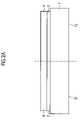
- FIGS. 1 A, 1 Bshow schematic cross-sections of a manufacturing method for an integrated semiconductor structure as a first embodiment of the present invention
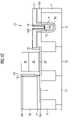
- the photoresist layer 15is stripped, and thereafter a trench 21 for an array MOSFET of RCAT type is formed by a suitable edge using the oxide layers 10 , 10 a as a mask. Then, the thin sacrificial oxide layer 10 is stripped, in which process step the thick oxide layer 10 a is correspondingly thinned.
Landscapes
- Engineering & Computer Science (AREA)
- Physics & Mathematics (AREA)
- Condensed Matter Physics & Semiconductors (AREA)
- General Physics & Mathematics (AREA)
- Manufacturing & Machinery (AREA)
- Computer Hardware Design (AREA)
- Microelectronics & Electronic Packaging (AREA)
- Power Engineering (AREA)
- Metal-Oxide And Bipolar Metal-Oxide Semiconductor Integrated Circuits (AREA)
- Electrodes Of Semiconductors (AREA)
- Semiconductor Memories (AREA)
Abstract
Description
Claims (14)
Priority Applications (7)
| Application Number | Priority Date | Filing Date | Title |
|---|---|---|---|
| US11/183,224US7202535B2 (en) | 2005-07-14 | 2005-07-14 | Manufacturing method for an integrated semiconductor structure and corresponding integrated semiconductor structure |
| DE102006029229ADE102006029229A1 (en) | 2005-07-14 | 2006-06-26 | Manufacturing method for an integrated semiconductor structure and corresponding integrated semiconductor structure |
| TW095123042ATWI298929B (en) | 2005-07-14 | 2006-06-26 | Manufacturing method for an integrated semiconductor structure and corresponding integrated semiconductor structure |
| KR1020060064753AKR100824947B1 (en) | 2005-07-14 | 2006-07-11 | Manufacturing method for an integrated semiconductor structure and corresponding integrated semiconductor structure |
| JP2006192767AJP2007027743A (en) | 2005-07-14 | 2006-07-13 | Integrated semiconductor structure manufacturing method and corresponding integrated semiconductor structure |
| CNA2006101063516ACN1905160A (en) | 2005-07-14 | 2006-07-14 | Manufacturing method for an integrated semiconductor structure and corresponding integrated semiconductor structure |
| US11/784,637US20070187774A1 (en) | 2005-07-14 | 2007-04-09 | Manufacturing method for an integrated semiconductor structure and corresponding integrated semiconductor structure |
Applications Claiming Priority (1)
| Application Number | Priority Date | Filing Date | Title |
|---|---|---|---|
| US11/183,224US7202535B2 (en) | 2005-07-14 | 2005-07-14 | Manufacturing method for an integrated semiconductor structure and corresponding integrated semiconductor structure |
Related Child Applications (1)
| Application Number | Title | Priority Date | Filing Date |
|---|---|---|---|
| US11/784,637ContinuationUS20070187774A1 (en) | 2005-07-14 | 2007-04-09 | Manufacturing method for an integrated semiconductor structure and corresponding integrated semiconductor structure |
Publications (2)
| Publication Number | Publication Date |
|---|---|
| US20070015325A1 US20070015325A1 (en) | 2007-01-18 |
| US7202535B2true US7202535B2 (en) | 2007-04-10 |
Family
ID=37662145
Family Applications (2)
| Application Number | Title | Priority Date | Filing Date |
|---|---|---|---|
| US11/183,224Expired - Fee RelatedUS7202535B2 (en) | 2005-07-14 | 2005-07-14 | Manufacturing method for an integrated semiconductor structure and corresponding integrated semiconductor structure |
| US11/784,637AbandonedUS20070187774A1 (en) | 2005-07-14 | 2007-04-09 | Manufacturing method for an integrated semiconductor structure and corresponding integrated semiconductor structure |
Family Applications After (1)
| Application Number | Title | Priority Date | Filing Date |
|---|---|---|---|
| US11/784,637AbandonedUS20070187774A1 (en) | 2005-07-14 | 2007-04-09 | Manufacturing method for an integrated semiconductor structure and corresponding integrated semiconductor structure |
Country Status (6)
| Country | Link |
|---|---|
| US (2) | US7202535B2 (en) |
| JP (1) | JP2007027743A (en) |
| KR (1) | KR100824947B1 (en) |
| CN (1) | CN1905160A (en) |
| DE (1) | DE102006029229A1 (en) |
| TW (1) | TWI298929B (en) |
Cited By (8)
| Publication number | Priority date | Publication date | Assignee | Title |
|---|---|---|---|---|
| US20070238031A1 (en)* | 2006-04-06 | 2007-10-11 | Lee Jang-Eun | Method for forming minute pattern and method for forming semiconductor memory device using the same |
| US20070262415A1 (en)* | 2006-05-11 | 2007-11-15 | Casey Smith | Recessed antifuse structures and methods of making the same |
| US20070264771A1 (en)* | 2006-05-11 | 2007-11-15 | Venkatesan Ananthan | Dual work function recessed access device and methods of forming |
| US20070262395A1 (en)* | 2006-05-11 | 2007-11-15 | Gibbons Jasper S | Memory cell access devices and methods of making the same |
| US20080057645A1 (en)* | 2006-09-05 | 2008-03-06 | Ememory Technology Inc. | Fabricating method of mosfet with thick gate dielectric layer |
| US20090008716A1 (en)* | 2007-06-27 | 2009-01-08 | Kabushiki Kaisha Toshiba | Semiconductor device and method of fabricating the same |
| US7824986B2 (en) | 2008-11-05 | 2010-11-02 | Micron Technology, Inc. | Methods of forming a plurality of transistor gates, and methods of forming a plurality of transistor gates having at least two different work functions |
| US8802522B2 (en) | 2010-09-10 | 2014-08-12 | Applied Materials, Inc. | Methods to adjust threshold voltage in semiconductor devices |
Families Citing this family (5)
| Publication number | Priority date | Publication date | Assignee | Title |
|---|---|---|---|---|
| KR101662282B1 (en)* | 2010-01-14 | 2016-10-05 | 삼성전자주식회사 | Semiconductor device having a buried gate pattern including high-k dielectric capping layer and fabricating method thereof |
| US8796751B2 (en)* | 2012-11-20 | 2014-08-05 | Micron Technology, Inc. | Transistors, memory cells and semiconductor constructions |
| TWI627749B (en)* | 2014-11-24 | 2018-06-21 | 聯華電子股份有限公司 | Semiconductor structure and semiconductor pattern structure |
| EP4120333A4 (en)* | 2021-04-28 | 2023-10-25 | Changxin Memory Technologies, Inc. | METHOD FOR PRODUCING A SEMICONDUCTOR STRUCTURE |
| CN115249655A (en)* | 2021-04-28 | 2022-10-28 | 长鑫存储技术有限公司 | Preparation method of semiconductor structure |
Citations (1)
| Publication number | Priority date | Publication date | Assignee | Title |
|---|---|---|---|---|
| US20050275035A1 (en)* | 2004-06-10 | 2005-12-15 | Agency For Science, Technology And Research | Gate Electrode Architecture for Improved Work Function Tuning and Method of Manufacture |
Family Cites Families (18)
| Publication number | Priority date | Publication date | Assignee | Title |
|---|---|---|---|---|
| US5298782A (en)* | 1991-06-03 | 1994-03-29 | Sgs-Thomson Microelectronics, Inc. | Stacked CMOS SRAM cell with polysilicon transistor load |
| KR970009276B1 (en)* | 1993-10-28 | 1997-06-09 | 금성일렉트론 주식회사 | Method for manufacturing moset |
| DE69433949T2 (en)* | 1993-12-07 | 2005-09-08 | Infineon Technologies Ag | Method of making MOSFETs with improved short channel effects |
| US6027705A (en)* | 1998-01-08 | 2000-02-22 | Showa Denko K.K. | Method for producing a higher silane |
| US6191460B1 (en)* | 1999-09-07 | 2001-02-20 | Integrated Device Technology, Inc. | Identical gate conductivity type static random access memory cell |
| JP4860022B2 (en)* | 2000-01-25 | 2012-01-25 | エルピーダメモリ株式会社 | Manufacturing method of semiconductor integrated circuit device |
| US6380088B1 (en)* | 2001-01-19 | 2002-04-30 | Chartered Semiconductor Manufacturing, Inc. | Method to form a recessed source drain on a trench side wall with a replacement gate technique |
| JP3944367B2 (en)* | 2001-02-06 | 2007-07-11 | 松下電器産業株式会社 | Method for forming insulating film and method for manufacturing semiconductor device |
| US6573134B2 (en)* | 2001-03-27 | 2003-06-03 | Sharp Laboratories Of America, Inc. | Dual metal gate CMOS devices and method for making the same |
| KR100399356B1 (en)* | 2001-04-11 | 2003-09-26 | 삼성전자주식회사 | Method of forming cmos type semiconductor device having dual gate |
| US6706581B1 (en)* | 2002-10-29 | 2004-03-16 | Taiwan Semiconductor Manufacturing Company | Dual gate dielectric scheme: SiON for high performance devices and high k for low power devices |
| US6930059B2 (en)* | 2003-02-27 | 2005-08-16 | Sharp Laboratories Of America, Inc. | Method for depositing a nanolaminate film by atomic layer deposition |
| KR100618815B1 (en)* | 2003-11-12 | 2006-08-31 | 삼성전자주식회사 | Semiconductor device having heterogeneous gate insulating film and manufacturing method thereof |
| TWI258811B (en)* | 2003-11-12 | 2006-07-21 | Samsung Electronics Co Ltd | Semiconductor devices having different gate dielectrics and methods for manufacturing the same |
| US7105889B2 (en)* | 2004-06-04 | 2006-09-12 | International Business Machines Corporation | Selective implementation of barrier layers to achieve threshold voltage control in CMOS device fabrication with high k dielectrics |
| US8399934B2 (en)* | 2004-12-20 | 2013-03-19 | Infineon Technologies Ag | Transistor device |
| US7416933B2 (en)* | 2004-08-06 | 2008-08-26 | Micron Technology, Inc. | Methods of enabling polysilicon gate electrodes for high-k gate dielectrics |
| US8679287B2 (en)* | 2005-05-23 | 2014-03-25 | Mks Instruments, Inc. | Method and apparatus for preventing ALD reactants from damaging vacuum pumps |
- 2005
- 2005-07-14USUS11/183,224patent/US7202535B2/ennot_activeExpired - Fee Related
- 2006
- 2006-06-26TWTW095123042Apatent/TWI298929B/ennot_activeIP Right Cessation
- 2006-06-26DEDE102006029229Apatent/DE102006029229A1/ennot_activeCeased
- 2006-07-11KRKR1020060064753Apatent/KR100824947B1/ennot_activeExpired - Fee Related
- 2006-07-13JPJP2006192767Apatent/JP2007027743A/enactivePending
- 2006-07-14CNCNA2006101063516Apatent/CN1905160A/enactivePending
- 2007
- 2007-04-09USUS11/784,637patent/US20070187774A1/ennot_activeAbandoned
Patent Citations (1)
| Publication number | Priority date | Publication date | Assignee | Title |
|---|---|---|---|---|
| US20050275035A1 (en)* | 2004-06-10 | 2005-12-15 | Agency For Science, Technology And Research | Gate Electrode Architecture for Improved Work Function Tuning and Method of Manufacture |
Cited By (19)
| Publication number | Priority date | Publication date | Assignee | Title |
|---|---|---|---|---|
| US20070238031A1 (en)* | 2006-04-06 | 2007-10-11 | Lee Jang-Eun | Method for forming minute pattern and method for forming semiconductor memory device using the same |
| US8083962B2 (en)* | 2006-04-06 | 2011-12-27 | Samsung Electronics Co., Ltd. | Method for forming minute pattern and method for forming semiconductor memory device using the same |
| US8692320B2 (en) | 2006-05-11 | 2014-04-08 | Micron Technology, Inc. | Recessed memory cell access devices and gate electrodes |
| US20070262415A1 (en)* | 2006-05-11 | 2007-11-15 | Casey Smith | Recessed antifuse structures and methods of making the same |
| US20070264771A1 (en)* | 2006-05-11 | 2007-11-15 | Venkatesan Ananthan | Dual work function recessed access device and methods of forming |
| US20070262395A1 (en)* | 2006-05-11 | 2007-11-15 | Gibbons Jasper S | Memory cell access devices and methods of making the same |
| US9543433B2 (en) | 2006-05-11 | 2017-01-10 | Micron Technology, Inc. | Dual work function recessed access device and methods of forming |
| US9502516B2 (en) | 2006-05-11 | 2016-11-22 | Micron Technology, Inc. | Recessed access devices and gate electrodes |
| US8860174B2 (en) | 2006-05-11 | 2014-10-14 | Micron Technology, Inc. | Recessed antifuse structures and methods of making the same |
| US8008144B2 (en)* | 2006-05-11 | 2011-08-30 | Micron Technology, Inc. | Dual work function recessed access device and methods of forming |
| US8710583B2 (en) | 2006-05-11 | 2014-04-29 | Micron Technology, Inc. | Dual work function recessed access device and methods of forming |
| US20080057645A1 (en)* | 2006-09-05 | 2008-03-06 | Ememory Technology Inc. | Fabricating method of mosfet with thick gate dielectric layer |
| US7932564B2 (en) | 2007-06-27 | 2011-04-26 | Kabushiki Kaisha Toshiba | Semiconductor device and method of fabricating the same |
| US20090008716A1 (en)* | 2007-06-27 | 2009-01-08 | Kabushiki Kaisha Toshiba | Semiconductor device and method of fabricating the same |
| US8524561B2 (en) | 2008-11-05 | 2013-09-03 | Micron Technology, Inc. | Methods of forming a plurality of transistor gates, and methods of forming a plurality of transistor gates having at least two different work functions |
| US8034687B2 (en) | 2008-11-05 | 2011-10-11 | Micron Technology, Inc. | Methods of forming a plurality of transistor gates, and methods of forming a plurality of transistor gates having at least two different work functions |
| US20110039404A1 (en)* | 2008-11-05 | 2011-02-17 | Micron Technology, Inc. | Methods of Forming a Plurality of Transistor Gates, and Methods of Forming a Plurality of Transistor Gates Having at Least Two Different Work Functions |
| US7824986B2 (en) | 2008-11-05 | 2010-11-02 | Micron Technology, Inc. | Methods of forming a plurality of transistor gates, and methods of forming a plurality of transistor gates having at least two different work functions |
| US8802522B2 (en) | 2010-09-10 | 2014-08-12 | Applied Materials, Inc. | Methods to adjust threshold voltage in semiconductor devices |
Also Published As
| Publication number | Publication date |
|---|---|
| US20070015325A1 (en) | 2007-01-18 |
| TW200703560A (en) | 2007-01-16 |
| KR100824947B1 (en) | 2008-04-28 |
| US20070187774A1 (en) | 2007-08-16 |
| JP2007027743A (en) | 2007-02-01 |
| KR20070009412A (en) | 2007-01-18 |
| TWI298929B (en) | 2008-07-11 |
| DE102006029229A1 (en) | 2007-02-15 |
| CN1905160A (en) | 2007-01-31 |
Similar Documents
| Publication | Publication Date | Title |
|---|---|---|
| US20070187774A1 (en) | Manufacturing method for an integrated semiconductor structure and corresponding integrated semiconductor structure | |
| US7446379B2 (en) | Transistor with dopant-bearing metal in source and drain | |
| US9659778B2 (en) | Methods of fabricating semiconductor devices and structures thereof | |
| US6706581B1 (en) | Dual gate dielectric scheme: SiON for high performance devices and high k for low power devices | |
| US6720630B2 (en) | Structure and method for MOSFET with metallic gate electrode | |
| US7754593B2 (en) | Semiconductor device and manufacturing method therefor | |
| US20070215951A1 (en) | Semiconductor devices having silicided electrodes | |
| JP4719161B2 (en) | Method for manufacturing transistor | |
| US20040137672A1 (en) | Triple layer hard mask for gate patterning to fabricate scaled cmos transistors | |
| KR101097964B1 (en) | Method for integrating a high-k gate dielectric in a transistor fabrication process | |
| JP5444176B2 (en) | Semiconductor device | |
| JP4110089B2 (en) | Manufacturing method of double gate type field effect transistor | |
| US6358798B1 (en) | Method for forming gate electrode by damascene process | |
| US7915128B2 (en) | High voltage semiconductor devices | |
| CN100421255C (en) | Fully depleted SOI multi-threshold voltage applications | |
| US6987038B2 (en) | Method for fabricating MOS field effect transistor | |
| KR100227644B1 (en) | Manufacturing method of a transistor | |
| KR20050101992A (en) | Flash memory cell transistor and method for fabrication the same | |
| KR100934828B1 (en) | MOSFET forming method of semiconductor device | |
| KR100564432B1 (en) | Transistor manufacturing method | |
| TW202510032A (en) | Semiconductor device and method for fabricating the same | |
| JP2001217416A (en) | Method for manufacturing semiconductor integrated circuit device | |
| KR20030049352A (en) | Method of manufacturing a semiconductor device | |
| JPH04360540A (en) | Manufacture of semiconductor device |
Legal Events
| Date | Code | Title | Description |
|---|---|---|---|
| AS | Assignment | Owner name:INFINEON TECHNOLOGIES AG, GERMANY Free format text:ASSIGNMENT OF ASSIGNORS INTEREST;ASSIGNORS:GOLDBACH, MATTHIAS;WU, DONGPING;REEL/FRAME:016796/0104 Effective date:20050818 | |
| FEPP | Fee payment procedure | Free format text:PAYOR NUMBER ASSIGNED (ORIGINAL EVENT CODE: ASPN); ENTITY STATUS OF PATENT OWNER: LARGE ENTITY | |
| STCF | Information on status: patent grant | Free format text:PATENTED CASE | |
| AS | Assignment | Owner name:QIMONDA AG, GERMANY Free format text:ASSIGNMENT OF ASSIGNORS INTEREST;ASSIGNOR:INFINEON TECHNOLOGIES AG;REEL/FRAME:023773/0001 Effective date:20060425 Owner name:QIMONDA AG,GERMANY Free format text:ASSIGNMENT OF ASSIGNORS INTEREST;ASSIGNOR:INFINEON TECHNOLOGIES AG;REEL/FRAME:023773/0001 Effective date:20060425 | |
| FPAY | Fee payment | Year of fee payment:4 | |
| FPAY | Fee payment | Year of fee payment:8 | |
| AS | Assignment | Owner name:INFINEON TECHNOLOGIES AG, GERMANY Free format text:ASSIGNMENT OF ASSIGNORS INTEREST;ASSIGNOR:QIMONDA AG;REEL/FRAME:035623/0001 Effective date:20141009 | |
| AS | Assignment | Owner name:POLARIS INNOVATIONS LIMITED, IRELAND Free format text:ASSIGNMENT OF ASSIGNORS INTEREST;ASSIGNOR:INFINEON TECHNOLOGIES AG;REEL/FRAME:036701/0926 Effective date:20150708 | |
| FEPP | Fee payment procedure | Free format text:MAINTENANCE FEE REMINDER MAILED (ORIGINAL EVENT CODE: REM.); ENTITY STATUS OF PATENT OWNER: LARGE ENTITY | |
| LAPS | Lapse for failure to pay maintenance fees | Free format text:PATENT EXPIRED FOR FAILURE TO PAY MAINTENANCE FEES (ORIGINAL EVENT CODE: EXP.); ENTITY STATUS OF PATENT OWNER: LARGE ENTITY | |
| STCH | Information on status: patent discontinuation | Free format text:PATENT EXPIRED DUE TO NONPAYMENT OF MAINTENANCE FEES UNDER 37 CFR 1.362 | |
| FP | Lapsed due to failure to pay maintenance fee | Effective date:20190410 |