US7202513B1 - Stress engineering using dual pad nitride with selective SOI device architecture - Google Patents
Stress engineering using dual pad nitride with selective SOI device architectureDownload PDFInfo
- Publication number
- US7202513B1 US7202513B1US11/162,953US16295305AUS7202513B1US 7202513 B1US7202513 B1US 7202513B1US 16295305 AUS16295305 AUS 16295305AUS 7202513 B1US7202513 B1US 7202513B1
- Authority
- US
- United States
- Prior art keywords
- regions
- stress
- semiconductor structure
- nitride
- nfet
- Prior art date
- Legal status (The legal status is an assumption and is not a legal conclusion. Google has not performed a legal analysis and makes no representation as to the accuracy of the status listed.)
- Expired - Lifetime
Links
Images


Classifications
- H—ELECTRICITY
- H10—SEMICONDUCTOR DEVICES; ELECTRIC SOLID-STATE DEVICES NOT OTHERWISE PROVIDED FOR
- H10D—INORGANIC ELECTRIC SEMICONDUCTOR DEVICES
- H10D86/00—Integrated devices formed in or on insulating or conducting substrates, e.g. formed in silicon-on-insulator [SOI] substrates or on stainless steel or glass substrates
- H10D86/201—Integrated devices formed in or on insulating or conducting substrates, e.g. formed in silicon-on-insulator [SOI] substrates or on stainless steel or glass substrates the substrates comprising an insulating layer on a semiconductor body, e.g. SOI
- H—ELECTRICITY
- H10—SEMICONDUCTOR DEVICES; ELECTRIC SOLID-STATE DEVICES NOT OTHERWISE PROVIDED FOR
- H10D—INORGANIC ELECTRIC SEMICONDUCTOR DEVICES
- H10D30/00—Field-effect transistors [FET]
- H10D30/60—Insulated-gate field-effect transistors [IGFET]
- H10D30/791—Arrangements for exerting mechanical stress on the crystal lattice of the channel regions
- H—ELECTRICITY
- H10—SEMICONDUCTOR DEVICES; ELECTRIC SOLID-STATE DEVICES NOT OTHERWISE PROVIDED FOR
- H10D—INORGANIC ELECTRIC SEMICONDUCTOR DEVICES
- H10D62/00—Semiconductor bodies, or regions thereof, of devices having potential barriers
- H10D62/10—Shapes, relative sizes or dispositions of the regions of the semiconductor bodies; Shapes of the semiconductor bodies
- H10D62/113—Isolations within a component, i.e. internal isolations
- H10D62/115—Dielectric isolations, e.g. air gaps
- H10D62/116—Dielectric isolations, e.g. air gaps adjoining the input or output regions of field-effect devices, e.g. adjoining source or drain regions
- H—ELECTRICITY
- H10—SEMICONDUCTOR DEVICES; ELECTRIC SOLID-STATE DEVICES NOT OTHERWISE PROVIDED FOR
- H10D—INORGANIC ELECTRIC SEMICONDUCTOR DEVICES
- H10D84/00—Integrated devices formed in or on semiconductor substrates that comprise only semiconducting layers, e.g. on Si wafers or on GaAs-on-Si wafers
- H10D84/01—Manufacture or treatment
- H10D84/0123—Integrating together multiple components covered by H10D12/00 or H10D30/00, e.g. integrating multiple IGBTs
- H10D84/0126—Integrating together multiple components covered by H10D12/00 or H10D30/00, e.g. integrating multiple IGBTs the components including insulated gates, e.g. IGFETs
- H10D84/0165—Integrating together multiple components covered by H10D12/00 or H10D30/00, e.g. integrating multiple IGBTs the components including insulated gates, e.g. IGFETs the components including complementary IGFETs, e.g. CMOS devices
- H10D84/0167—Manufacturing their channels
- H—ELECTRICITY
- H10—SEMICONDUCTOR DEVICES; ELECTRIC SOLID-STATE DEVICES NOT OTHERWISE PROVIDED FOR
- H10D—INORGANIC ELECTRIC SEMICONDUCTOR DEVICES
- H10D84/00—Integrated devices formed in or on semiconductor substrates that comprise only semiconducting layers, e.g. on Si wafers or on GaAs-on-Si wafers
- H10D84/01—Manufacture or treatment
- H10D84/0123—Integrating together multiple components covered by H10D12/00 or H10D30/00, e.g. integrating multiple IGBTs
- H10D84/0126—Integrating together multiple components covered by H10D12/00 or H10D30/00, e.g. integrating multiple IGBTs the components including insulated gates, e.g. IGFETs
- H10D84/0165—Integrating together multiple components covered by H10D12/00 or H10D30/00, e.g. integrating multiple IGBTs the components including insulated gates, e.g. IGFETs the components including complementary IGFETs, e.g. CMOS devices
- H10D84/017—Manufacturing their source or drain regions, e.g. silicided source or drain regions
- H—ELECTRICITY
- H10—SEMICONDUCTOR DEVICES; ELECTRIC SOLID-STATE DEVICES NOT OTHERWISE PROVIDED FOR
- H10D—INORGANIC ELECTRIC SEMICONDUCTOR DEVICES
- H10D84/00—Integrated devices formed in or on semiconductor substrates that comprise only semiconducting layers, e.g. on Si wafers or on GaAs-on-Si wafers
- H10D84/01—Manufacture or treatment
- H10D84/0123—Integrating together multiple components covered by H10D12/00 or H10D30/00, e.g. integrating multiple IGBTs
- H10D84/0126—Integrating together multiple components covered by H10D12/00 or H10D30/00, e.g. integrating multiple IGBTs the components including insulated gates, e.g. IGFETs
- H10D84/0165—Integrating together multiple components covered by H10D12/00 or H10D30/00, e.g. integrating multiple IGBTs the components including insulated gates, e.g. IGFETs the components including complementary IGFETs, e.g. CMOS devices
- H10D84/0188—Manufacturing their isolation regions
- H—ELECTRICITY
- H10—SEMICONDUCTOR DEVICES; ELECTRIC SOLID-STATE DEVICES NOT OTHERWISE PROVIDED FOR
- H10D—INORGANIC ELECTRIC SEMICONDUCTOR DEVICES
- H10D84/00—Integrated devices formed in or on semiconductor substrates that comprise only semiconducting layers, e.g. on Si wafers or on GaAs-on-Si wafers
- H10D84/01—Manufacture or treatment
- H10D84/02—Manufacture or treatment characterised by using material-based technologies
- H10D84/03—Manufacture or treatment characterised by using material-based technologies using Group IV technology, e.g. silicon technology or silicon-carbide [SiC] technology
- H10D84/038—Manufacture or treatment characterised by using material-based technologies using Group IV technology, e.g. silicon technology or silicon-carbide [SiC] technology using silicon technology, e.g. SiGe
- H—ELECTRICITY
- H10—SEMICONDUCTOR DEVICES; ELECTRIC SOLID-STATE DEVICES NOT OTHERWISE PROVIDED FOR
- H10D—INORGANIC ELECTRIC SEMICONDUCTOR DEVICES
- H10D86/00—Integrated devices formed in or on insulating or conducting substrates, e.g. formed in silicon-on-insulator [SOI] substrates or on stainless steel or glass substrates
- H10D86/01—Manufacture or treatment
Definitions
- FIG. 1illustrates the selective SOI architecture used in the present invention.
- the SOI architecture 10comprises a top Si-containing semiconductor layer 16 and a bottom Si-containing semiconductor layer 12 , wherein portions of the top Si-containing semiconductor layer 16 are separated from the Si-containing semiconductor layer 12 by discrete buried oxide regions 14 .
- the discrete buried oxide regions 14are present underneath areas of the top Si-containing semiconductor layer that will eventually receive the source/drain junctions of a MOS transistor. No discrete buried oxide is present underneath areas of the top Si-containing semiconductor layer in which the MOS channel will be present.
- the selective SOI architecture used in the present inventionhas been described previously in co-pending and co-assigned U.S. patent application Ser. No. 10/604,102, filed Jun. 26, 2003 and Ser. No. 10/754,320, filed Jan. 8, 2004, the entire contents of which are both incorporated herein by reference. Note that FIG. 1 also shows the presence of trench isolation regions which are labeled as STI.
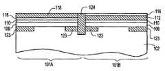
- the resultant structure, in one embodiment of the present invention, including the patterned first nitride film 112 atop the unpatterned pad oxide 110is shown in FIG. 5 .
- the patterned first nitride film 112is shown over the second device region 101 B, the present invention also contemplates the case when the patterned first nitride film 112 is located only over the first device region 101 A.
- the structure shown in FIG. 10is then subjected to another planarization process which removes any remaining pad oxide and nitride films from the structure and thereafter MOS devices are formed on the surface of the planarized structure utilizing a conventional CMOS process.
- This step of the present inventionprovides the structure illustrated in FIG. 11 wherein a first FET 126 of a first conductivity type is formed in the first device region 101 A and a second FET 128 of a second conductivity type that is different from the first conductivity type is formed in the second device region 101 B.
- an nFETis formed in the region that is under tensile strain, while a pFET is formed in the region under compressive strain.
- channel regions 136are stressed without the need of using a conventional stress liner and/or embedded stress regions.
- high stressed channelare formed into the Si-containing material by providing lateral voids in a structure that includes dual stress nitride pad films. These pad films, which are used in forming the STI region are removed from the structure and then CMOS devices are formed thereon.
Landscapes
- Metal-Oxide And Bipolar Metal-Oxide Semiconductor Integrated Circuits (AREA)
- Thin Film Transistor (AREA)
- Insulated Gate Type Field-Effect Transistor (AREA)
- Element Separation (AREA)
- Local Oxidation Of Silicon (AREA)
Abstract
Description
forming a trench into said first and second material stacks between said first and second device regions that extends down though at least one of said n-doped regions;
laterally etching said n-doped regions to create voids on each side of the trench which maintain stress of said overlying nitride films; and
filling said voids and trench with an oxide.
Claims (10)
Priority Applications (4)
| Application Number | Priority Date | Filing Date | Title |
|---|---|---|---|
| US11/162,953US7202513B1 (en) | 2005-09-29 | 2005-09-29 | Stress engineering using dual pad nitride with selective SOI device architecture |
| CNB2006101157388ACN100464425C (en) | 2005-09-29 | 2006-08-15 | Semiconductor structure and manufacturing method thereof |
| TW095134233ATW200717800A (en) | 2005-09-29 | 2006-09-15 | Stress engineering using dual pad nitride with selective SOI device architecture |
| US11/668,790US7550364B2 (en) | 2005-09-29 | 2007-01-30 | Stress engineering using dual pad nitride with selective SOI device architecture |
Applications Claiming Priority (1)
| Application Number | Priority Date | Filing Date | Title |
|---|---|---|---|
| US11/162,953US7202513B1 (en) | 2005-09-29 | 2005-09-29 | Stress engineering using dual pad nitride with selective SOI device architecture |
Related Child Applications (1)
| Application Number | Title | Priority Date | Filing Date |
|---|---|---|---|
| US11/668,790DivisionUS7550364B2 (en) | 2005-09-29 | 2007-01-30 | Stress engineering using dual pad nitride with selective SOI device architecture |
Publications (2)
| Publication Number | Publication Date |
|---|---|
| US20070069294A1 US20070069294A1 (en) | 2007-03-29 |
| US7202513B1true US7202513B1 (en) | 2007-04-10 |
Family
ID=37892811
Family Applications (2)
| Application Number | Title | Priority Date | Filing Date |
|---|---|---|---|
| US11/162,953Expired - LifetimeUS7202513B1 (en) | 2005-09-29 | 2005-09-29 | Stress engineering using dual pad nitride with selective SOI device architecture |
| US11/668,790Expired - Fee RelatedUS7550364B2 (en) | 2005-09-29 | 2007-01-30 | Stress engineering using dual pad nitride with selective SOI device architecture |
Family Applications After (1)
| Application Number | Title | Priority Date | Filing Date |
|---|---|---|---|
| US11/668,790Expired - Fee RelatedUS7550364B2 (en) | 2005-09-29 | 2007-01-30 | Stress engineering using dual pad nitride with selective SOI device architecture |
Country Status (3)
| Country | Link |
|---|---|
| US (2) | US7202513B1 (en) |
| CN (1) | CN100464425C (en) |
| TW (1) | TW200717800A (en) |
Cited By (15)
| Publication number | Priority date | Publication date | Assignee | Title |
|---|---|---|---|---|
| US20080169508A1 (en)* | 2007-01-11 | 2008-07-17 | International Business Machines Corporation | Stressed soi fet having doped glass box layer |
| US20090050972A1 (en)* | 2007-08-20 | 2009-02-26 | Richard Lindsay | Strained Semiconductor Device and Method of Making Same |
| KR100899646B1 (en) | 2007-06-12 | 2009-05-27 | 삼성전자주식회사 | Semiconductor device and method of forming the same |
| US20090194821A1 (en)* | 2008-01-31 | 2009-08-06 | Akio Kaneko | Semiconductor device and method of fabricating the same |
| US20090250763A1 (en)* | 2007-08-23 | 2009-10-08 | Gerhard Knoblinger | Integrated circuit including a first channel and a second channel |
| US20100047977A1 (en)* | 2006-03-17 | 2010-02-25 | Acorn Technologies, Inc. | Strained silicon with elastic edge relaxation |
| US7700416B1 (en)* | 2008-04-25 | 2010-04-20 | Acorn Technologies, Inc. | Tensile strained semiconductor on insulator using elastic edge relaxation and a sacrificial stressor layer |
| US20100211098A1 (en)* | 2008-02-20 | 2010-08-19 | Ahmad Robert Hadba | Compound Barb Medical Device and Method |
| US20100269075A1 (en)* | 2009-04-20 | 2010-10-21 | William Robert Tonti | Method and system for selective stress enablement in simulation modeling |
| US8361868B2 (en) | 2010-04-28 | 2013-01-29 | Acorn Technologies, Inc. | Transistor with longitudinal strain in channel induced by buried stressor relaxed by implantation |
| US8361867B2 (en) | 2010-03-19 | 2013-01-29 | Acorn Technologies, Inc. | Biaxial strained field effect transistor devices |
| US8395213B2 (en) | 2010-08-27 | 2013-03-12 | Acorn Technologies, Inc. | Strained semiconductor using elastic edge relaxation of a stressor combined with buried insulating layer |
| US9059201B2 (en) | 2010-04-28 | 2015-06-16 | Acorn Technologies, Inc. | Transistor with longitudinal strain in channel induced by buried stressor relaxed by implantation |
| US9406798B2 (en) | 2010-08-27 | 2016-08-02 | Acorn Technologies, Inc. | Strained semiconductor using elastic edge relaxation of a stressor combined with buried insulating layer |
| US10833194B2 (en) | 2010-08-27 | 2020-11-10 | Acorn Semi, Llc | SOI wafers and devices with buried stressor |
Families Citing this family (17)
| Publication number | Priority date | Publication date | Assignee | Title |
|---|---|---|---|---|
| US8530355B2 (en)* | 2005-12-23 | 2013-09-10 | Infineon Technologies Ag | Mixed orientation semiconductor device and method |
| US7829407B2 (en) | 2006-11-20 | 2010-11-09 | International Business Machines Corporation | Method of fabricating a stressed MOSFET by bending SOI region |
| US20080237733A1 (en)* | 2007-03-27 | 2008-10-02 | International Business Machines Corporation | Structure and method to enhance channel stress by using optimized sti stress and nitride capping layer stress |
| US8263466B2 (en)* | 2007-10-17 | 2012-09-11 | Acorn Technologies, Inc. | Channel strain induced by strained metal in FET source or drain |
| KR100937599B1 (en)* | 2007-12-17 | 2010-01-20 | 한국전자통신연구원 | Semiconductor Device and Forming Method |
| US8274115B2 (en)* | 2008-03-19 | 2012-09-25 | Globalfoundries Singapore Pte. Ltd. | Hybrid orientation substrate with stress layer |
| US8022488B2 (en)* | 2009-09-24 | 2011-09-20 | International Business Machines Corporation | High-performance FETs with embedded stressors |
| US8835994B2 (en)* | 2010-06-01 | 2014-09-16 | International Business Machines Corporation | Reduced corner leakage in SOI structure and method |
| CN102064177B (en)* | 2010-11-11 | 2012-09-26 | 电子科技大学 | CMOS (Complementary Metal Oxide Semiconductor) transistor structure with stress amplification |
| CN101924107B (en)* | 2010-07-15 | 2012-09-26 | 电子科技大学 | Stress enhanced CMOS (Complementary Metal-Oxide-Semiconductor) transistor structure |
| US8647935B2 (en) | 2010-12-17 | 2014-02-11 | International Business Machines Corporation | Buried oxidation for enhanced mobility |
| US8642430B2 (en)* | 2012-04-09 | 2014-02-04 | GlobalFoundries, Inc. | Processes for preparing stressed semiconductor wafers and for preparing devices including the stressed semiconductor wafers |
| US20130285117A1 (en)* | 2012-04-27 | 2013-10-31 | International Business Machines Corporation | CMOS WITH SiGe CHANNEL PFETs AND METHOD OF FABRICATION |
| CN102916047B (en)* | 2012-10-23 | 2015-09-30 | 哈尔滨工程大学 | SOI body contact structure and the formation method of oxygen corrosion technology are buried in a kind of utilization |
| US9018057B1 (en) | 2013-10-08 | 2015-04-28 | Stmicroelectronics, Inc. | Method of making a CMOS semiconductor device using a stressed silicon-on-insulator (SOI) wafer |
| US9196544B2 (en) | 2014-03-14 | 2015-11-24 | Globalfoundries Singapore Pte. Ltd. | Integrated circuits with stressed semiconductor-on-insulator (SOI) body contacts and methods for fabricating the same |
| US11450573B2 (en)* | 2020-06-17 | 2022-09-20 | Globalfoundries U.S. Inc. | Structure with different stress-inducing isolation dielectrics for different polarity FETs |
Citations (74)
| Publication number | Priority date | Publication date | Assignee | Title |
|---|---|---|---|---|
| US3602841A (en) | 1970-06-18 | 1971-08-31 | Ibm | High frequency bulk semiconductor amplifiers and oscillators |
| US4665415A (en) | 1985-04-24 | 1987-05-12 | International Business Machines Corporation | Semiconductor device with hole conduction via strained lattice |
| JPS6476755A (en) | 1987-09-18 | 1989-03-22 | Hitachi Ltd | Semiconductor device |
| US4853076A (en) | 1983-12-29 | 1989-08-01 | Massachusetts Institute Of Technology | Semiconductor thin films |
| US4855245A (en) | 1985-09-13 | 1989-08-08 | Siemens Aktiengesellschaft | Method of manufacturing integrated circuit containing bipolar and complementary MOS transistors on a common substrate |
| US4952524A (en) | 1989-05-05 | 1990-08-28 | At&T Bell Laboratories | Semiconductor device manufacture including trench formation |
| US4958213A (en) | 1987-12-07 | 1990-09-18 | Texas Instruments Incorporated | Method for forming a transistor base region under thick oxide |
| US5006913A (en) | 1988-11-05 | 1991-04-09 | Mitsubishi Denki Kabushiki Kaisha | Stacked type semiconductor device |
| US5060030A (en) | 1990-07-18 | 1991-10-22 | Raytheon Company | Pseudomorphic HEMT having strained compensation layer |
| US5081513A (en) | 1991-02-28 | 1992-01-14 | Xerox Corporation | Electronic device with recovery layer proximate to active layer |
| US5108843A (en) | 1988-11-30 | 1992-04-28 | Ricoh Company, Ltd. | Thin film semiconductor and process for producing the same |
| US5134085A (en) | 1991-11-21 | 1992-07-28 | Micron Technology, Inc. | Reduced-mask, split-polysilicon CMOS process, incorporating stacked-capacitor cells, for fabricating multi-megabit dynamic random access memories |
| US5310446A (en) | 1990-01-10 | 1994-05-10 | Ricoh Company, Ltd. | Method for producing semiconductor film |
| US5354695A (en) | 1992-04-08 | 1994-10-11 | Leedy Glenn J | Membrane dielectric isolation IC fabrication |
| US5371399A (en) | 1991-06-14 | 1994-12-06 | International Business Machines Corporation | Compound semiconductor having metallic inclusions and devices fabricated therefrom |
| US5391510A (en) | 1992-02-28 | 1995-02-21 | International Business Machines Corporation | Formation of self-aligned metal gate FETs using a benignant removable gate material during high temperature steps |
| US5459346A (en) | 1988-06-28 | 1995-10-17 | Ricoh Co., Ltd. | Semiconductor substrate with electrical contact in groove |
| US5557122A (en) | 1995-05-12 | 1996-09-17 | Alliance Semiconductors Corporation | Semiconductor electrode having improved grain structure and oxide growth properties |
| US5561302A (en) | 1994-09-26 | 1996-10-01 | Motorola, Inc. | Enhanced mobility MOSFET device and method |
| US5670798A (en) | 1995-03-29 | 1997-09-23 | North Carolina State University | Integrated heterostructures of Group III-V nitride semiconductor materials including epitaxial ohmic contact non-nitride buffer layer and methods of fabricating same |
| US5679965A (en) | 1995-03-29 | 1997-10-21 | North Carolina State University | Integrated heterostructures of Group III-V nitride semiconductor materials including epitaxial ohmic contact, non-nitride buffer layer and methods of fabricating same |
| US5861651A (en) | 1997-02-28 | 1999-01-19 | Lucent Technologies Inc. | Field effect devices and capacitors with improved thin film dielectrics and method for making same |
| US5880040A (en) | 1996-04-15 | 1999-03-09 | Macronix International Co., Ltd. | Gate dielectric based on oxynitride grown in N2 O and annealed in NO |
| US5940736A (en) | 1997-03-11 | 1999-08-17 | Lucent Technologies Inc. | Method for forming a high quality ultrathin gate oxide layer |
| US5940716A (en) | 1996-03-15 | 1999-08-17 | Samsung Electronics Co., Ltd. | Methods of forming trench isolation regions using repatterned trench masks |
| US5960297A (en) | 1997-07-02 | 1999-09-28 | Kabushiki Kaisha Toshiba | Shallow trench isolation structure and method of forming the same |
| US5989978A (en) | 1998-07-16 | 1999-11-23 | Chartered Semiconductor Manufacturing, Ltd. | Shallow trench isolation of MOSFETS with reduced corner parasitic currents |
| US6008126A (en) | 1992-04-08 | 1999-12-28 | Elm Technology Corporation | Membrane dielectric isolation IC fabrication |
| US6025280A (en) | 1997-04-28 | 2000-02-15 | Lucent Technologies Inc. | Use of SiD4 for deposition of ultra thin and controllable oxides |
| US6066545A (en) | 1997-12-09 | 2000-05-23 | Texas Instruments Incorporated | Birdsbeak encroachment using combination of wet and dry etch for isolation nitride |
| US6090684A (en) | 1998-07-31 | 2000-07-18 | Hitachi, Ltd. | Method for manufacturing semiconductor device |
| US6107143A (en) | 1998-03-02 | 2000-08-22 | Samsung Electronics Co., Ltd. | Method for forming a trench isolation structure in an integrated circuit |
| US6110769A (en)* | 1997-12-15 | 2000-08-29 | Lg Semicon Co., Ltd. | SOI (silicon on insulator) device and method for fabricating the same |
| US6117722A (en) | 1999-02-18 | 2000-09-12 | Taiwan Semiconductor Manufacturing Company | SRAM layout for relaxing mechanical stress in shallow trench isolation technology and method of manufacture thereof |
| US6133071A (en) | 1997-10-15 | 2000-10-17 | Nec Corporation | Semiconductor device with plate heat sink free from cracks due to thermal stress and process for assembling it with package |
| US6165383A (en) | 1998-04-10 | 2000-12-26 | Organic Display Technology | Useful precursors for organic electroluminescent materials and devices made from such materials |
| US6221735B1 (en) | 2000-02-15 | 2001-04-24 | Philips Semiconductors, Inc. | Method for eliminating stress induced dislocations in CMOS devices |
| US6228694B1 (en) | 1999-06-28 | 2001-05-08 | Intel Corporation | Method of increasing the mobility of MOS transistors by use of localized stress regions |
| US6255169B1 (en) | 1999-02-22 | 2001-07-03 | Advanced Micro Devices, Inc. | Process for fabricating a high-endurance non-volatile memory device |
| US6261964B1 (en) | 1997-03-14 | 2001-07-17 | Micron Technology, Inc. | Material removal method for forming a structure |
| US6265317B1 (en) | 2001-01-09 | 2001-07-24 | Taiwan Semiconductor Manufacturing Company | Top corner rounding for shallow trench isolation |
| US20010009784A1 (en) | 1998-01-09 | 2001-07-26 | Yanjun Ma | Structure and method of making a sub-micron MOS transistor |
| US6274444B1 (en) | 1999-07-30 | 2001-08-14 | United Microelectronics Corp. | Method for forming mosfet |
| US6281532B1 (en) | 1999-06-28 | 2001-08-28 | Intel Corporation | Technique to obtain increased channel mobilities in NMOS transistors by gate electrode engineering |
| US6284626B1 (en) | 1999-04-06 | 2001-09-04 | Vantis Corporation | Angled nitrogen ion implantation for minimizing mechanical stress on side walls of an isolation trench |
| US6284623B1 (en) | 1999-10-25 | 2001-09-04 | Peng-Fei Zhang | Method of fabricating semiconductor devices using shallow trench isolation with reduced narrow channel effect |
| US6319794B1 (en) | 1998-10-14 | 2001-11-20 | International Business Machines Corporation | Structure and method for producing low leakage isolation devices |
| US6362082B1 (en) | 1999-06-28 | 2002-03-26 | Intel Corporation | Methodology for control of short channel effects in MOS transistors |
| US6361885B1 (en) | 1998-04-10 | 2002-03-26 | Organic Display Technology | Organic electroluminescent materials and device made from such materials |
| US6368931B1 (en) | 2000-03-27 | 2002-04-09 | Intel Corporation | Thin tensile layers in shallow trench isolation and method of making same |
| US20020063292A1 (en) | 2000-11-29 | 2002-05-30 | Mark Armstrong | CMOS fabrication process utilizing special transistor orientation |
| US6403486B1 (en) | 2001-04-30 | 2002-06-11 | Taiwan Semiconductor Manufacturing Company | Method for forming a shallow trench isolation |
| US6403975B1 (en) | 1996-04-09 | 2002-06-11 | Max-Planck Gesellschaft Zur Forderung Der Wissenschafteneev | Semiconductor components, in particular photodetectors, light emitting diodes, optical modulators and waveguides with multilayer structures grown on silicon substrates |
| US6406973B1 (en) | 1999-06-29 | 2002-06-18 | Hyundai Electronics Industries Co., Ltd. | Transistor in a semiconductor device and method of manufacturing the same |
| US20020086472A1 (en) | 2000-12-29 | 2002-07-04 | Brian Roberds | Technique to obtain high mobility channels in MOS transistors by forming a strain layer on an underside of a channel |
| US20020086497A1 (en) | 2000-12-30 | 2002-07-04 | Kwok Siang Ping | Beaker shape trench with nitride pull-back for STI |
| US20020090791A1 (en) | 1999-06-28 | 2002-07-11 | Brian S. Doyle | Method for reduced capacitance interconnect system using gaseous implants into the ild |
| US6461936B1 (en) | 2002-01-04 | 2002-10-08 | Infineon Technologies Ag | Double pullback method of filling an isolation trench |
| US6476462B2 (en) | 1999-12-28 | 2002-11-05 | Texas Instruments Incorporated | MOS-type semiconductor device and method for making same |
| US6483171B1 (en) | 1999-08-13 | 2002-11-19 | Micron Technology, Inc. | Vertical sub-micron CMOS transistors on (110), (111), (311), (511), and higher order surfaces of bulk, SOI and thin film structures and method of forming same |
| US6493497B1 (en) | 2000-09-26 | 2002-12-10 | Motorola, Inc. | Electro-optic structure and process for fabricating same |
| US6498358B1 (en) | 2001-07-20 | 2002-12-24 | Motorola, Inc. | Structure and method for fabricating an electro-optic system having an electrochromic diffraction grating |
| US6501121B1 (en) | 2000-11-15 | 2002-12-31 | Motorola, Inc. | Semiconductor structure |
| US6506652B2 (en) | 1998-11-13 | 2003-01-14 | Intel Corporation | Method of recessing spacers to improved salicide resistance on polysilicon gates |
| US20030032261A1 (en) | 2001-08-08 | 2003-02-13 | Ling-Yen Yeh | Method of preventing threshold voltage of MOS transistor from being decreased by shallow trench isolation formation |
| US20030040158A1 (en) | 2001-08-21 | 2003-02-27 | Nec Corporation | Semiconductor device and method of fabricating the same |
| US6531740B2 (en) | 2001-07-17 | 2003-03-11 | Motorola, Inc. | Integrated impedance matching and stability network |
| US6531369B1 (en) | 2000-03-01 | 2003-03-11 | Applied Micro Circuits Corporation | Heterojunction bipolar transistor (HBT) fabrication using a selectively deposited silicon germanium (SiGe) |
| US20030057184A1 (en) | 2001-09-22 | 2003-03-27 | Shiuh-Sheng Yu | Method for pull back SiN to increase rounding effect in a shallow trench isolation process |
| US20030067035A1 (en) | 2001-09-28 | 2003-04-10 | Helmut Tews | Gate processing method with reduced gate oxide corner and edge thinning |
| US6621392B1 (en) | 2002-04-25 | 2003-09-16 | International Business Machines Corporation | Micro electromechanical switch having self-aligned spacers |
| US6635506B2 (en) | 2001-11-07 | 2003-10-21 | International Business Machines Corporation | Method of fabricating micro-electromechanical switches on CMOS compatible substrates |
| US6831292B2 (en) | 2001-09-21 | 2004-12-14 | Amberwave Systems Corporation | Semiconductor structures employing strained material layers with defined impurity gradients and methods for fabricating same |
| US7005302B2 (en)* | 2004-04-07 | 2006-02-28 | Advanced Micro Devices, Inc. | Semiconductor on insulator substrate and devices formed therefrom |
Family Cites Families (26)
| Publication number | Priority date | Publication date | Assignee | Title |
|---|---|---|---|---|
| US3602A (en)* | 1844-05-25 | Tenoning and mortising machine | ||
| DE3419392C1 (en) | 1984-05-24 | 1985-12-05 | Deutsche Texaco Ag, 2000 Hamburg | Process for the continuous production of isopropyl alcohol or sec. Butyl alcohol |
| US4888300A (en)* | 1985-11-07 | 1989-12-19 | Fairchild Camera And Instrument Corporation | Submerged wall isolation of silicon islands |
| WO1994027317A1 (en) | 1993-05-06 | 1994-11-24 | Siemens Aktiengesellschaft | Process for producing components on an soi substrate |
| US5427975A (en)* | 1993-05-10 | 1995-06-27 | Delco Electronics Corporation | Method of micromachining an integrated sensor on the surface of a silicon wafer |
| US6074903A (en) | 1998-06-16 | 2000-06-13 | Siemens Aktiengesellschaft | Method for forming electrical isolation for semiconductor devices |
| JP4521542B2 (en) | 1999-03-30 | 2010-08-11 | ルネサスエレクトロニクス株式会社 | Semiconductor device and semiconductor substrate |
| US6326667B1 (en) | 1999-09-09 | 2001-12-04 | Kabushiki Kaisha Toshiba | Semiconductor devices and methods for producing semiconductor devices |
| WO2002044156A2 (en) | 2000-11-29 | 2002-06-06 | Glaxo Group Limited | Benzimidazole derivatives useful as tie-2 and/or vegfr-2 inhibitors |
| US6603156B2 (en) | 2001-03-31 | 2003-08-05 | International Business Machines Corporation | Strained silicon on insulator structures |
| JP2002305293A (en) | 2001-04-06 | 2002-10-18 | Canon Inc | Semiconductor member manufacturing method and semiconductor device manufacturing method |
| US6825529B2 (en)* | 2002-12-12 | 2004-11-30 | International Business Machines Corporation | Stress inducing spacers |
| US6774015B1 (en) | 2002-12-19 | 2004-08-10 | International Business Machines Corporation | Strained silicon-on-insulator (SSOI) and method to form the same |
| US6825086B2 (en)* | 2003-01-17 | 2004-11-30 | Sharp Laboratories Of America, Inc. | Strained-silicon channel CMOS with sacrificial shallow trench isolation oxide liner |
| US6815738B2 (en) | 2003-02-28 | 2004-11-09 | International Business Machines Corporation | Multiple gate MOSFET structure with strained Si Fin body |
| US6828628B2 (en) | 2003-03-05 | 2004-12-07 | Agere Systems, Inc. | Diffused MOS devices with strained silicon portions and methods for forming same |
| US6955952B2 (en)* | 2003-03-07 | 2005-10-18 | Taiwan Semiconductor Manufacturing Company, Ltd. | Strain balanced structure with a tensile strained silicon channel and a compressive strained silicon-germanium channel for CMOS performance enhancement |
| US6900502B2 (en)* | 2003-04-03 | 2005-05-31 | Taiwan Semiconductor Manufacturing Company, Ltd. | Strained channel on insulator device |
| US6882025B2 (en)* | 2003-04-25 | 2005-04-19 | Taiwan Semiconductor Manufacturing Company, Ltd. | Strained-channel transistor and methods of manufacture |
| US6936522B2 (en)* | 2003-06-26 | 2005-08-30 | International Business Machines Corporation | Selective silicon-on-insulator isolation structure and method |
| US6815278B1 (en) | 2003-08-25 | 2004-11-09 | International Business Machines Corporation | Ultra-thin silicon-on-insulator and strained-silicon-direct-on-insulator with hybrid crystal orientations |
| US6767802B1 (en) | 2003-09-19 | 2004-07-27 | Sharp Laboratories Of America, Inc. | Methods of making relaxed silicon-germanium on insulator via layer transfer |
| US6958516B2 (en) | 2004-01-08 | 2005-10-25 | International Business Machines Corporation | Discriminative SOI with oxide holes underneath DC source/drain |
| WO2005112129A1 (en)* | 2004-05-13 | 2005-11-24 | Fujitsu Limited | Semiconductor device and process for fabricating same, and process for producing semiconductor substrate |
| US7262087B2 (en)* | 2004-12-14 | 2007-08-28 | International Business Machines Corporation | Dual stressed SOI substrates |
| US7384861B2 (en)* | 2005-07-18 | 2008-06-10 | Texas Instruments Incorporated | Strain modulation employing process techniques for CMOS technologies |
- 2005
- 2005-09-29USUS11/162,953patent/US7202513B1/ennot_activeExpired - Lifetime
- 2006
- 2006-08-15CNCNB2006101157388Apatent/CN100464425C/ennot_activeExpired - Fee Related
- 2006-09-15TWTW095134233Apatent/TW200717800A/enunknown
- 2007
- 2007-01-30USUS11/668,790patent/US7550364B2/ennot_activeExpired - Fee Related
Patent Citations (87)
| Publication number | Priority date | Publication date | Assignee | Title |
|---|---|---|---|---|
| US3602841A (en) | 1970-06-18 | 1971-08-31 | Ibm | High frequency bulk semiconductor amplifiers and oscillators |
| US4853076A (en) | 1983-12-29 | 1989-08-01 | Massachusetts Institute Of Technology | Semiconductor thin films |
| US4665415A (en) | 1985-04-24 | 1987-05-12 | International Business Machines Corporation | Semiconductor device with hole conduction via strained lattice |
| US4855245A (en) | 1985-09-13 | 1989-08-08 | Siemens Aktiengesellschaft | Method of manufacturing integrated circuit containing bipolar and complementary MOS transistors on a common substrate |
| JPS6476755A (en) | 1987-09-18 | 1989-03-22 | Hitachi Ltd | Semiconductor device |
| US4958213A (en) | 1987-12-07 | 1990-09-18 | Texas Instruments Incorporated | Method for forming a transistor base region under thick oxide |
| US5459346A (en) | 1988-06-28 | 1995-10-17 | Ricoh Co., Ltd. | Semiconductor substrate with electrical contact in groove |
| US5565697A (en) | 1988-06-28 | 1996-10-15 | Ricoh Company, Ltd. | Semiconductor structure having island forming grooves |
| US5006913A (en) | 1988-11-05 | 1991-04-09 | Mitsubishi Denki Kabushiki Kaisha | Stacked type semiconductor device |
| US5108843A (en) | 1988-11-30 | 1992-04-28 | Ricoh Company, Ltd. | Thin film semiconductor and process for producing the same |
| US4952524A (en) | 1989-05-05 | 1990-08-28 | At&T Bell Laboratories | Semiconductor device manufacture including trench formation |
| US5310446A (en) | 1990-01-10 | 1994-05-10 | Ricoh Company, Ltd. | Method for producing semiconductor film |
| US5060030A (en) | 1990-07-18 | 1991-10-22 | Raytheon Company | Pseudomorphic HEMT having strained compensation layer |
| US5081513A (en) | 1991-02-28 | 1992-01-14 | Xerox Corporation | Electronic device with recovery layer proximate to active layer |
| US5471948A (en) | 1991-06-14 | 1995-12-05 | International Business Machines Corporation | Method of making a compound semiconductor having metallic inclusions |
| US5371399A (en) | 1991-06-14 | 1994-12-06 | International Business Machines Corporation | Compound semiconductor having metallic inclusions and devices fabricated therefrom |
| US5134085A (en) | 1991-11-21 | 1992-07-28 | Micron Technology, Inc. | Reduced-mask, split-polysilicon CMOS process, incorporating stacked-capacitor cells, for fabricating multi-megabit dynamic random access memories |
| US5391510A (en) | 1992-02-28 | 1995-02-21 | International Business Machines Corporation | Formation of self-aligned metal gate FETs using a benignant removable gate material during high temperature steps |
| US5946559A (en) | 1992-04-08 | 1999-08-31 | Elm Technology Corporation | Membrane dielectric isolation IC fabrication |
| US5354695A (en) | 1992-04-08 | 1994-10-11 | Leedy Glenn J | Membrane dielectric isolation IC fabrication |
| US5571741A (en) | 1992-04-08 | 1996-11-05 | Leedy; Glenn J. | Membrane dielectric isolation IC fabrication |
| US5592018A (en) | 1992-04-08 | 1997-01-07 | Leedy; Glenn J. | Membrane dielectric isolation IC fabrication |
| US5592007A (en) | 1992-04-08 | 1997-01-07 | Leedy; Glenn J. | Membrane dielectric isolation transistor fabrication |
| US5840593A (en) | 1992-04-08 | 1998-11-24 | Elm Technology Corporation | Membrane dielectric isolation IC fabrication |
| US6008126A (en) | 1992-04-08 | 1999-12-28 | Elm Technology Corporation | Membrane dielectric isolation IC fabrication |
| US5561302A (en) | 1994-09-26 | 1996-10-01 | Motorola, Inc. | Enhanced mobility MOSFET device and method |
| US5683934A (en) | 1994-09-26 | 1997-11-04 | Motorola, Inc. | Enhanced mobility MOSFET device and method |
| US5670798A (en) | 1995-03-29 | 1997-09-23 | North Carolina State University | Integrated heterostructures of Group III-V nitride semiconductor materials including epitaxial ohmic contact non-nitride buffer layer and methods of fabricating same |
| US5679965A (en) | 1995-03-29 | 1997-10-21 | North Carolina State University | Integrated heterostructures of Group III-V nitride semiconductor materials including epitaxial ohmic contact, non-nitride buffer layer and methods of fabricating same |
| US6046464A (en) | 1995-03-29 | 2000-04-04 | North Carolina State University | Integrated heterostructures of group III-V nitride semiconductor materials including epitaxial ohmic contact comprising multiple quantum well |
| US5557122A (en) | 1995-05-12 | 1996-09-17 | Alliance Semiconductors Corporation | Semiconductor electrode having improved grain structure and oxide growth properties |
| US5940716A (en) | 1996-03-15 | 1999-08-17 | Samsung Electronics Co., Ltd. | Methods of forming trench isolation regions using repatterned trench masks |
| US6403975B1 (en) | 1996-04-09 | 2002-06-11 | Max-Planck Gesellschaft Zur Forderung Der Wissenschafteneev | Semiconductor components, in particular photodetectors, light emitting diodes, optical modulators and waveguides with multilayer structures grown on silicon substrates |
| US5880040A (en) | 1996-04-15 | 1999-03-09 | Macronix International Co., Ltd. | Gate dielectric based on oxynitride grown in N2 O and annealed in NO |
| US5861651A (en) | 1997-02-28 | 1999-01-19 | Lucent Technologies Inc. | Field effect devices and capacitors with improved thin film dielectrics and method for making same |
| US5940736A (en) | 1997-03-11 | 1999-08-17 | Lucent Technologies Inc. | Method for forming a high quality ultrathin gate oxide layer |
| US6246095B1 (en) | 1997-03-11 | 2001-06-12 | Agere Systems Guardian Corp. | System and method for forming a uniform thin gate oxide layer |
| US6261964B1 (en) | 1997-03-14 | 2001-07-17 | Micron Technology, Inc. | Material removal method for forming a structure |
| US6025280A (en) | 1997-04-28 | 2000-02-15 | Lucent Technologies Inc. | Use of SiD4 for deposition of ultra thin and controllable oxides |
| US5960297A (en) | 1997-07-02 | 1999-09-28 | Kabushiki Kaisha Toshiba | Shallow trench isolation structure and method of forming the same |
| US6133071A (en) | 1997-10-15 | 2000-10-17 | Nec Corporation | Semiconductor device with plate heat sink free from cracks due to thermal stress and process for assembling it with package |
| US6066545A (en) | 1997-12-09 | 2000-05-23 | Texas Instruments Incorporated | Birdsbeak encroachment using combination of wet and dry etch for isolation nitride |
| US6110769A (en)* | 1997-12-15 | 2000-08-29 | Lg Semicon Co., Ltd. | SOI (silicon on insulator) device and method for fabricating the same |
| US20010009784A1 (en) | 1998-01-09 | 2001-07-26 | Yanjun Ma | Structure and method of making a sub-micron MOS transistor |
| US6107143A (en) | 1998-03-02 | 2000-08-22 | Samsung Electronics Co., Ltd. | Method for forming a trench isolation structure in an integrated circuit |
| US6165383A (en) | 1998-04-10 | 2000-12-26 | Organic Display Technology | Useful precursors for organic electroluminescent materials and devices made from such materials |
| US6361885B1 (en) | 1998-04-10 | 2002-03-26 | Organic Display Technology | Organic electroluminescent materials and device made from such materials |
| US5989978A (en) | 1998-07-16 | 1999-11-23 | Chartered Semiconductor Manufacturing, Ltd. | Shallow trench isolation of MOSFETS with reduced corner parasitic currents |
| US6090684A (en) | 1998-07-31 | 2000-07-18 | Hitachi, Ltd. | Method for manufacturing semiconductor device |
| US6319794B1 (en) | 1998-10-14 | 2001-11-20 | International Business Machines Corporation | Structure and method for producing low leakage isolation devices |
| US6509618B2 (en) | 1998-11-13 | 2003-01-21 | Intel Corporation | Device having thin first spacers and partially recessed thick second spacers for improved salicide resistance on polysilicon gates |
| US6521964B1 (en) | 1998-11-13 | 2003-02-18 | Intel Corporation | Device having spacers for improved salicide resistance on polysilicon gates |
| US6506652B2 (en) | 1998-11-13 | 2003-01-14 | Intel Corporation | Method of recessing spacers to improved salicide resistance on polysilicon gates |
| US6117722A (en) | 1999-02-18 | 2000-09-12 | Taiwan Semiconductor Manufacturing Company | SRAM layout for relaxing mechanical stress in shallow trench isolation technology and method of manufacture thereof |
| US6255169B1 (en) | 1999-02-22 | 2001-07-03 | Advanced Micro Devices, Inc. | Process for fabricating a high-endurance non-volatile memory device |
| US6284626B1 (en) | 1999-04-06 | 2001-09-04 | Vantis Corporation | Angled nitrogen ion implantation for minimizing mechanical stress on side walls of an isolation trench |
| US20020074598A1 (en) | 1999-06-28 | 2002-06-20 | Doyle Brian S. | Methodology for control of short channel effects in MOS transistors |
| US6281532B1 (en) | 1999-06-28 | 2001-08-28 | Intel Corporation | Technique to obtain increased channel mobilities in NMOS transistors by gate electrode engineering |
| US20020090791A1 (en) | 1999-06-28 | 2002-07-11 | Brian S. Doyle | Method for reduced capacitance interconnect system using gaseous implants into the ild |
| US6228694B1 (en) | 1999-06-28 | 2001-05-08 | Intel Corporation | Method of increasing the mobility of MOS transistors by use of localized stress regions |
| US6362082B1 (en) | 1999-06-28 | 2002-03-26 | Intel Corporation | Methodology for control of short channel effects in MOS transistors |
| US6406973B1 (en) | 1999-06-29 | 2002-06-18 | Hyundai Electronics Industries Co., Ltd. | Transistor in a semiconductor device and method of manufacturing the same |
| US6274444B1 (en) | 1999-07-30 | 2001-08-14 | United Microelectronics Corp. | Method for forming mosfet |
| US6483171B1 (en) | 1999-08-13 | 2002-11-19 | Micron Technology, Inc. | Vertical sub-micron CMOS transistors on (110), (111), (311), (511), and higher order surfaces of bulk, SOI and thin film structures and method of forming same |
| US6284623B1 (en) | 1999-10-25 | 2001-09-04 | Peng-Fei Zhang | Method of fabricating semiconductor devices using shallow trench isolation with reduced narrow channel effect |
| US6476462B2 (en) | 1999-12-28 | 2002-11-05 | Texas Instruments Incorporated | MOS-type semiconductor device and method for making same |
| US6221735B1 (en) | 2000-02-15 | 2001-04-24 | Philips Semiconductors, Inc. | Method for eliminating stress induced dislocations in CMOS devices |
| US6531369B1 (en) | 2000-03-01 | 2003-03-11 | Applied Micro Circuits Corporation | Heterojunction bipolar transistor (HBT) fabrication using a selectively deposited silicon germanium (SiGe) |
| US6368931B1 (en) | 2000-03-27 | 2002-04-09 | Intel Corporation | Thin tensile layers in shallow trench isolation and method of making same |
| US6493497B1 (en) | 2000-09-26 | 2002-12-10 | Motorola, Inc. | Electro-optic structure and process for fabricating same |
| US6501121B1 (en) | 2000-11-15 | 2002-12-31 | Motorola, Inc. | Semiconductor structure |
| US20020063292A1 (en) | 2000-11-29 | 2002-05-30 | Mark Armstrong | CMOS fabrication process utilizing special transistor orientation |
| US20020086472A1 (en) | 2000-12-29 | 2002-07-04 | Brian Roberds | Technique to obtain high mobility channels in MOS transistors by forming a strain layer on an underside of a channel |
| US20020086497A1 (en) | 2000-12-30 | 2002-07-04 | Kwok Siang Ping | Beaker shape trench with nitride pull-back for STI |
| US6265317B1 (en) | 2001-01-09 | 2001-07-24 | Taiwan Semiconductor Manufacturing Company | Top corner rounding for shallow trench isolation |
| US6403486B1 (en) | 2001-04-30 | 2002-06-11 | Taiwan Semiconductor Manufacturing Company | Method for forming a shallow trench isolation |
| US6531740B2 (en) | 2001-07-17 | 2003-03-11 | Motorola, Inc. | Integrated impedance matching and stability network |
| US6498358B1 (en) | 2001-07-20 | 2002-12-24 | Motorola, Inc. | Structure and method for fabricating an electro-optic system having an electrochromic diffraction grating |
| US20030032261A1 (en) | 2001-08-08 | 2003-02-13 | Ling-Yen Yeh | Method of preventing threshold voltage of MOS transistor from being decreased by shallow trench isolation formation |
| US20030040158A1 (en) | 2001-08-21 | 2003-02-27 | Nec Corporation | Semiconductor device and method of fabricating the same |
| US6831292B2 (en) | 2001-09-21 | 2004-12-14 | Amberwave Systems Corporation | Semiconductor structures employing strained material layers with defined impurity gradients and methods for fabricating same |
| US20030057184A1 (en) | 2001-09-22 | 2003-03-27 | Shiuh-Sheng Yu | Method for pull back SiN to increase rounding effect in a shallow trench isolation process |
| US20030067035A1 (en) | 2001-09-28 | 2003-04-10 | Helmut Tews | Gate processing method with reduced gate oxide corner and edge thinning |
| US6635506B2 (en) | 2001-11-07 | 2003-10-21 | International Business Machines Corporation | Method of fabricating micro-electromechanical switches on CMOS compatible substrates |
| US6461936B1 (en) | 2002-01-04 | 2002-10-08 | Infineon Technologies Ag | Double pullback method of filling an isolation trench |
| US6621392B1 (en) | 2002-04-25 | 2003-09-16 | International Business Machines Corporation | Micro electromechanical switch having self-aligned spacers |
| US7005302B2 (en)* | 2004-04-07 | 2006-02-28 | Advanced Micro Devices, Inc. | Semiconductor on insulator substrate and devices formed therefrom |
Non-Patent Citations (23)
| Title |
|---|
| A. Shimizu, et al., "Local Mechanical-Stress Control (LMC): A New Technique for CMOS-Performance Enhancement." International Electron Devices Meeting, IEEE, Mar. 2001. |
| B. Doyle, et al., "Recovery of Hot-Carrier Damage in Reoxidized Nitrided Oxide MOSFETs." IEEE Electron Device Letters, vol. 13, No. 1, Jan. 1992, pp. 38-40. |
| C.J. Huang, et al., "Temperature Dependence and Post-Stress Recovery of Hot Electron Degradation Effects in Bipolar Transistors." IEEE 1991 Bipolar Circuits and Technology Meeting 7.5, pp. 170-173. |
| D.C. Houghton, et al., "Equilibrium Critical Thickness for SI 1-x GEx Strained Layers on (100) Si". Appl. Phys. Lett. 56 (5), Jan. 29, 1990, pp. 460-462. |
| F. Ootsuka, et al., "A Highly Dense, High-Performance 130 nm Node CMOS Technology for Large Scale System-on-a-Chip Application." International Electron Devices Meeting 23.5.1, IEEE, Apr. 2000. |
| G. Zhang, et al., "A New 'Mixed-Mode' Reliability Degradation Mechanism in Advanced Si and SiGe Bipolar Transistors." IEEE Transactions on Electron Devices, vol. 49, No. 12, Dec. 2002, pp. 2151-2156. |
| Gregory Scott, et al., "NMOS Drive Current Reduction Caused by Transistor Layout and Trench Isolation Induced Stress." International Electron Devices Meeting, 34.4.1, IEEE, Sep. 1999. |
| H. Li, et al., "Design of W-Band VCOs with High Output Power for Potential Application in 77 GHz Automotive Radar Systems." 2003 IEEE GaAs Digest, pp. 263-266. |
| H. Wurzer, et al., "Annealing of Degraded npn-Transistors- Mechanisms and Modeling." IEEE Transactions on Electron Devices, vol. 41, No. 4, Apr. 1994, pp. 533-538. |
| H.S. Momose, et al., "Analysis of the Temperature Dependence of Hot-Carrier-Induced Degradation in Bipolar Transistors for Bi-CMOS." IEEE Transactions on Electron Devices, vol. 41, No. 6, Jun. 1994, pp. 978-987. |
| H.S. Momose, et al., "Temperature Dependence of Emitter-Base Reverse Stress Degradation and its Mechanism Analyzed by MOS Structures." Paper 6.2, pp. 140-143. |
| J.C. Bean, et al., "GEx SI 1-x/Si Strained-Layer Superlattice Grown by Molecular Beam Epitaxy". J. Vac. Sci. Technol. A 2(2), Apr.-Jun. 1984, pp. 436-440. |
| J.H. Van Der Merwe, "Regular Articles". Journal of Applied Physics, vol. 34, No. 1, Jan. 1963, pp. 117-122. |
| J.W. Matthews, et al., "Defects in Epitaxial Multilayers". Journal of Crystal Growth 27 (1974), pp. 118-125. |
| K. Ota, et al., "Novel Locally Strained Channel Technique for High Performance 55nm CMOS." International Electron Devices Meeting, 2.2.1, IEEE, Feb. 2002. |
| Kern Rim, et al., "Characteristics and Device Design of Sub-100 nm Strained Si N- and PMOSFETs." 2002 Symposium on VLSI Technology Digest of Technical Papers, IEEE, pp. 98-99. |
| Kern Rim, et al., "Transconductance Enhancement in Deep Submicron Strained-Si n-MOSFETs". International Electron Devices Meeting, 26, 8, 1, IEEE, Sep. 1998. |
| M. Khater, et al., "SiGe HBT Technology with Fmax/Ft=350/300 GHz and Gate Delay Below 3.3 ps". 2004 IEEE, 4 pages. |
| R.H.M. Van De Leur, et al., "Critical Thickness for Pseudomorphic Growth of Si/Ge Alloys and Superlattices". J. Appl. Phys. 64 (6), Sep. 15, 1988, pp. 3043-3050. |
| S.R. Sheng, et al., "Degradation and Recovery of SiGe HBTs Following Radiation and Hot-Carrier Stressing." pp. 14-15. |
| Shinya Ito, et al., "Mechanical Stress Effect of Etch-Stop Nitride and its Impact on Deep Submicron Transistor Design." International Electron Device Meeting, 10.7.1, IEEE, Apr. 2000. |
| Subramaniam S. Iyer, et al., "Heterojunction Bipolar Transistors Using Si-Ge Alloys". IEEE Transactions on Electron Devices, vol. 36, No. 10, Oct. 1989, pp. 2043-2064. |
| Z. Yang, et al., "Avalanche Current Induced Hot Carrier Degradation in 200 GHz SiGe Heterojunction Bipolar Transistors." pp. 1-5. |
Cited By (29)
| Publication number | Priority date | Publication date | Assignee | Title |
|---|---|---|---|---|
| US20100047977A1 (en)* | 2006-03-17 | 2010-02-25 | Acorn Technologies, Inc. | Strained silicon with elastic edge relaxation |
| US7977147B2 (en) | 2006-03-17 | 2011-07-12 | Acom Technologies, Inc. | Strained silicon with elastic edge relaxation |
| US7888197B2 (en)* | 2007-01-11 | 2011-02-15 | International Business Machines Corporation | Method of forming stressed SOI FET having doped glass box layer using sacrificial stressed layer |
| US20080169508A1 (en)* | 2007-01-11 | 2008-07-17 | International Business Machines Corporation | Stressed soi fet having doped glass box layer |
| KR100899646B1 (en) | 2007-06-12 | 2009-05-27 | 삼성전자주식회사 | Semiconductor device and method of forming the same |
| US20090050972A1 (en)* | 2007-08-20 | 2009-02-26 | Richard Lindsay | Strained Semiconductor Device and Method of Making Same |
| US8877576B2 (en) | 2007-08-23 | 2014-11-04 | Infineon Technologies Ag | Integrated circuit including a first channel and a second channel |
| US20090250763A1 (en)* | 2007-08-23 | 2009-10-08 | Gerhard Knoblinger | Integrated circuit including a first channel and a second channel |
| US20090194821A1 (en)* | 2008-01-31 | 2009-08-06 | Akio Kaneko | Semiconductor device and method of fabricating the same |
| US8039333B2 (en)* | 2008-01-31 | 2011-10-18 | Kabushiki Kaisha Toshiba | Semiconductor device and method of fabricating the same |
| US20100211098A1 (en)* | 2008-02-20 | 2010-08-19 | Ahmad Robert Hadba | Compound Barb Medical Device and Method |
| TWI469340B (en)* | 2008-04-25 | 2015-01-11 | Acorn Tech Inc | Overlying semiconductor with elastic edge relaxation and sacrificial stress layer |
| US7700416B1 (en)* | 2008-04-25 | 2010-04-20 | Acorn Technologies, Inc. | Tensile strained semiconductor on insulator using elastic edge relaxation and a sacrificial stressor layer |
| US20100269075A1 (en)* | 2009-04-20 | 2010-10-21 | William Robert Tonti | Method and system for selective stress enablement in simulation modeling |
| US8112729B2 (en) | 2009-04-20 | 2012-02-07 | International Business Machines Corporation | Method and system for selective stress enablement in simulation modeling |
| US8361867B2 (en) | 2010-03-19 | 2013-01-29 | Acorn Technologies, Inc. | Biaxial strained field effect transistor devices |
| US9059201B2 (en) | 2010-04-28 | 2015-06-16 | Acorn Technologies, Inc. | Transistor with longitudinal strain in channel induced by buried stressor relaxed by implantation |
| US8361868B2 (en) | 2010-04-28 | 2013-01-29 | Acorn Technologies, Inc. | Transistor with longitudinal strain in channel induced by buried stressor relaxed by implantation |
| US10833194B2 (en) | 2010-08-27 | 2020-11-10 | Acorn Semi, Llc | SOI wafers and devices with buried stressor |
| US9406798B2 (en) | 2010-08-27 | 2016-08-02 | Acorn Technologies, Inc. | Strained semiconductor using elastic edge relaxation of a stressor combined with buried insulating layer |
| US10084091B2 (en) | 2010-08-27 | 2018-09-25 | Acorn Technologies, Inc. | Strained semiconductor using elastic edge relaxation of a stressor combined with buried insulating layer |
| US10580896B2 (en) | 2010-08-27 | 2020-03-03 | Acorn Semi, Llc | Strained semiconductor using elastic edge relaxation of a stressor combined with buried insulating layer |
| US8395213B2 (en) | 2010-08-27 | 2013-03-12 | Acorn Technologies, Inc. | Strained semiconductor using elastic edge relaxation of a stressor combined with buried insulating layer |
| US10950727B2 (en) | 2010-08-27 | 2021-03-16 | Acorn Semi, Llc | Strained semiconductor using elastic edge relaxation of a stressor combined with buried insulating layer |
| US11322615B2 (en) | 2010-08-27 | 2022-05-03 | Acorn Semi, Llc | SOI wafers and devices with buried stressor |
| US11476364B2 (en) | 2010-08-27 | 2022-10-18 | Acorn Semi, Llc | Strained semiconductor using elastic edge relaxation of a stressor combined with buried insulating layer |
| US11791411B2 (en) | 2010-08-27 | 2023-10-17 | Acorn Semi, Llc | Relating to SOI wafers and devices with buried stressors |
| US11978800B2 (en) | 2010-08-27 | 2024-05-07 | Acorn Semi, Llc | Strained semiconductor using elastic edge relaxation of a stressor combined with buried insulating layer |
| US12402365B2 (en) | 2010-08-27 | 2025-08-26 | Acorn Semi, Llc | SOI wafers and devices with buried stressors |
Also Published As
| Publication number | Publication date |
|---|---|
| CN1941387A (en) | 2007-04-04 |
| TW200717800A (en) | 2007-05-01 |
| US20070122965A1 (en) | 2007-05-31 |
| CN100464425C (en) | 2009-02-25 |
| US7550364B2 (en) | 2009-06-23 |
| US20070069294A1 (en) | 2007-03-29 |
Similar Documents
| Publication | Publication Date | Title |
|---|---|---|
| US7550364B2 (en) | Stress engineering using dual pad nitride with selective SOI device architecture | |
| US10714616B2 (en) | FINFET having a gate structure in a trench feature in a bent fin | |
| US6882025B2 (en) | Strained-channel transistor and methods of manufacture | |
| US8012820B2 (en) | Ultra-thin SOI CMOS with raised epitaxial source and drain and embedded SiGe PFET extension | |
| US7825477B2 (en) | Semiconductor device with localized stressor | |
| US7425483B2 (en) | Structure and method of fabricating a hybrid substrate for high-performance hybrid-orientation silicon-on-insulator CMOS devices | |
| US7528050B2 (en) | High performance field effect transistors on SOI substrate with stress-inducing material as buried insulator and methods | |
| US7678634B2 (en) | Local stress engineering for CMOS devices | |
| US7928443B2 (en) | Method and structure for forming strained SI for CMOS devices | |
| US20020115240A1 (en) | Double soi device with recess etch and epitaxy | |
| US6869866B1 (en) | Silicide proximity structures for CMOS device performance improvements | |
| US20060145274A1 (en) | NFETs using gate induced stress modulation | |
| US20080128765A1 (en) | MOSFET Device With Localized Stressor | |
| KR20090073183A (en) | Stress type field effect transistor and its manufacturing method | |
| US9564488B2 (en) | Strained isolation regions | |
| US20090305471A1 (en) | Thin silicon single diffusion field effect transistor for enhanced drive performance with stress film liners |
Legal Events
| Date | Code | Title | Description |
|---|---|---|---|
| AS | Assignment | Owner name:INTERNATIONAL BUSINESS MACHINES CORPORATION, NEW Y Free format text:ASSIGNMENT OF ASSIGNORS INTEREST;ASSIGNORS:CHIDAMBARRAO, DURESETI;HENSON, WILLIAM K.;RIM, KERN;AND OTHERS;REEL/FRAME:016598/0748;SIGNING DATES FROM 20050915 TO 20050923 | |
| FEPP | Fee payment procedure | Free format text:PAYOR NUMBER ASSIGNED (ORIGINAL EVENT CODE: ASPN); ENTITY STATUS OF PATENT OWNER: LARGE ENTITY | |
| STCF | Information on status: patent grant | Free format text:PATENTED CASE | |
| FPAY | Fee payment | Year of fee payment:4 | |
| REMI | Maintenance fee reminder mailed | ||
| FPAY | Fee payment | Year of fee payment:8 | |
| SULP | Surcharge for late payment | Year of fee payment:7 | |
| AS | Assignment | Owner name:GLOBALFOUNDRIES U.S. 2 LLC, NEW YORK Free format text:ASSIGNMENT OF ASSIGNORS INTEREST;ASSIGNOR:INTERNATIONAL BUSINESS MACHINES CORPORATION;REEL/FRAME:036550/0001 Effective date:20150629 | |
| AS | Assignment | Owner name:GLOBALFOUNDRIES INC., CAYMAN ISLANDS Free format text:ASSIGNMENT OF ASSIGNORS INTEREST;ASSIGNORS:GLOBALFOUNDRIES U.S. 2 LLC;GLOBALFOUNDRIES U.S. INC.;REEL/FRAME:036779/0001 Effective date:20150910 | |
| MAFP | Maintenance fee payment | Free format text:PAYMENT OF MAINTENANCE FEE, 12TH YEAR, LARGE ENTITY (ORIGINAL EVENT CODE: M1553); ENTITY STATUS OF PATENT OWNER: LARGE ENTITY Year of fee payment:12 | |
| AS | Assignment | Owner name:WILMINGTON TRUST, NATIONAL ASSOCIATION, DELAWARE Free format text:SECURITY AGREEMENT;ASSIGNOR:GLOBALFOUNDRIES INC.;REEL/FRAME:049490/0001 Effective date:20181127 | |
| AS | Assignment | Owner name:GLOBALFOUNDRIES U.S. INC., CALIFORNIA Free format text:ASSIGNMENT OF ASSIGNORS INTEREST;ASSIGNOR:GLOBALFOUNDRIES INC.;REEL/FRAME:054633/0001 Effective date:20201022 | |
| AS | Assignment | Owner name:GLOBALFOUNDRIES INC., CAYMAN ISLANDS Free format text:RELEASE BY SECURED PARTY;ASSIGNOR:WILMINGTON TRUST, NATIONAL ASSOCIATION;REEL/FRAME:054636/0001 Effective date:20201117 | |
| AS | Assignment | Owner name:GLOBALFOUNDRIES U.S. INC., NEW YORK Free format text:RELEASE BY SECURED PARTY;ASSIGNOR:WILMINGTON TRUST, NATIONAL ASSOCIATION;REEL/FRAME:056987/0001 Effective date:20201117 |