US7200719B2 - Prefetch control in a data processing system - Google Patents
Prefetch control in a data processing systemDownload PDFInfo
- Publication number
- US7200719B2 US7200719B2US10/631,136US63113603AUS7200719B2US 7200719 B2US7200719 B2US 7200719B2US 63113603 AUS63113603 AUS 63113603AUS 7200719 B2US7200719 B2US 7200719B2
- Authority
- US
- United States
- Prior art keywords
- prefetch
- master
- buffer
- counter
- prefetches
- Prior art date
- Legal status (The legal status is an assumption and is not a legal conclusion. Google has not performed a legal analysis and makes no representation as to the accuracy of the status listed.)
- Expired - Lifetime
Links
Images


Classifications
- G—PHYSICS
- G06—COMPUTING OR CALCULATING; COUNTING
- G06F—ELECTRIC DIGITAL DATA PROCESSING
- G06F13/00—Interconnection of, or transfer of information or other signals between, memories, input/output devices or central processing units
- G06F13/14—Handling requests for interconnection or transfer
- G—PHYSICS
- G06—COMPUTING OR CALCULATING; COUNTING
- G06F—ELECTRIC DIGITAL DATA PROCESSING
- G06F12/00—Accessing, addressing or allocating within memory systems or architectures
- G06F12/02—Addressing or allocation; Relocation
- G06F12/0215—Addressing or allocation; Relocation with look ahead addressing means
- G—PHYSICS
- G06—COMPUTING OR CALCULATING; COUNTING
- G06F—ELECTRIC DIGITAL DATA PROCESSING
- G06F12/00—Accessing, addressing or allocating within memory systems or architectures
- G—PHYSICS
- G06—COMPUTING OR CALCULATING; COUNTING
- G06F—ELECTRIC DIGITAL DATA PROCESSING
- G06F13/00—Interconnection of, or transfer of information or other signals between, memories, input/output devices or central processing units
- Y—GENERAL TAGGING OF NEW TECHNOLOGICAL DEVELOPMENTS; GENERAL TAGGING OF CROSS-SECTIONAL TECHNOLOGIES SPANNING OVER SEVERAL SECTIONS OF THE IPC; TECHNICAL SUBJECTS COVERED BY FORMER USPC CROSS-REFERENCE ART COLLECTIONS [XRACs] AND DIGESTS
- Y02—TECHNOLOGIES OR APPLICATIONS FOR MITIGATION OR ADAPTATION AGAINST CLIMATE CHANGE
- Y02D—CLIMATE CHANGE MITIGATION TECHNOLOGIES IN INFORMATION AND COMMUNICATION TECHNOLOGIES [ICT], I.E. INFORMATION AND COMMUNICATION TECHNOLOGIES AIMING AT THE REDUCTION OF THEIR OWN ENERGY USE
- Y02D10/00—Energy efficient computing, e.g. low power processors, power management or thermal management
Definitions
- the present inventionrelates to a data processing system, and more particularly, to prefetch control within a data processing system.
- Prefetchingis commonly used to access information within a data processing system. By prefetching information in advance of a request for that information, the latency caused by accessing the information requested by the bus master may be reduced. However, in typical prefetching schemes a number of prefetches are wasted since the bus master may not request access to the prefetched information. Another disadvantage of general prefetching schemes is that the prefetch limit control provided by such systems is based on a fixed policy, allowing less flexibility and control. Therefore, a need exists for a method of prefetching that reduces the number of prefetches that are wasted, resulting in a reduced amount of power consumption and an optimization of data processor performance.
- FIG. 1illustrates, in block diagram form, a data processing system in accordance with one embodiment of the present invention
- FIG. 2illustrates, in block diagram form, a control register of the data processing system of FIG. 1 , in accordance with one embodiment of the present invention
- FIG. 3illustrates, in block diagram form, prefetch counters of the data processing system of FIG. 1 , in accordance with one embodiment of the present invention
- FIG. 4illustrates, in table form, field descriptions of the control register of FIG. 2 in accordance with one embodiment of the present invention.
- FIG. 5illustrates, in flow diagram form, operation of the data processing system of FIG. 1 in accordance with one embodiment of the present invention.
- busis used to refer to a plurality of signals or conductors which may be used to transfer one or more various types of information, such as data, addresses, control, or status.
- the conductors as discussed hereinmay be illustrated or described in reference to being a single conductor, a plurality of conductors, unidirectional conductors, or bidirectional conductors. However, different embodiments may vary the implementation of the conductors. For example, separate unidirectional conductors may be used rather than bidirectional conductors and vice versa.
- plurality of conductorsmay be replaced with a single conductor that transfers multiple signals serially or in a time multiplexed manner. Likewise, single conductors carrying multiple signals may be separated out into various different conductors carrying subsets of these signals. Therefore, many options exist for transferring signals.
- One embodiment of the present inventionrelates to dynamically controlling the number of sequential prefetch operations in order to prevent wasted prefetches. For example, by limiting the number of sequential prefetches performed after a buffer miss, the performance and power consumption of the memory control unit can be optimized. In one embodiment, limiting the number of sequential prefetches is accomplished by using a set of prefetch buffers, a control register, and prefetch counters, all of which will be further described below. In another embodiment, a software programmable control scheme is provided which allows for dynamic control of the number of sequential prefetch operations between buffer misses and may be preprogrammed by the user based upon the properties of the requesting master.
- a central processing unitFor example, within a central processing unit (CPU) instructions are typically executed sequentially until a change of flow instruction or an exception is reached, which causes a discontinuity in sequential execution.
- the number of instructions executed sequentiallyis dependent upon the CPU and is a function of the type of application program being executed. Some applications show extended sequential execution, while others behave more erratically, with frequent change of flow events. Therefore, depending on the application, the desired number of prefetches may differ.
- a DMA masteris provided in which transfers occur sequentially until an end-of-transfer or a channel switch occurs. For this example, long sequences are expected and the prefetch limit corresponding to the DMA master can be adjusted accordingly.
- One embodiment of the present inventionrelates to a data processing system including a master, storage circuitry coupled to the master, a control storage circuit which stores a prefetch limit, a prefetch buffer, and prefetch circuitry coupled to the control storage circuit, prefetch buffer, and storage circuitry.
- the prefetch circuitryselectively prefetches a predetermined number of lines from the storage circuitry into the prefetch buffer, wherein the prefetch limit controls the number of prefetches that occur between misses in the prefetch buffer.
- Another embodiment of the present inventionrelates to a method for performing prefetch in a data processing system.
- a plurality of access requests from a master to access storage circuitryis received and a prefetch limit is used to limit a number of prefetches performed between misses in a prefetch buffer resulting from at least a portion of the plurality of access requests.
- a prefetch control circuitis provided to store the prefetch limit.
- Yet another embodiment of the present inventionrelates to a method for performing a prefetch in a data processing system in which a read request from a master to access storage circuitry is received and it is determined whether the read request results in a hit or a miss in a prefetch buffer.
- a prefetchis selectively performed of a predetermined number of lines from the storage circuitry into the prefetch buffer based at least in part on a prefetch counter reaching a first value.
- a demand fetchis performed in response to the read request and the prefetch counter is set to a second value.
- FIG. 1illustrates one embodiment of data processing system 10 .
- Data processing system 10includes a master 12 (also referred to as an interconnect master 12 ), a master 14 (also referred to as an interconnect master 14 ), a memory array controller 36 , a system interconnect 22 , I/O circuitry 16 , a peripheral 18 , other slaves 20 , and a memory array 35 .
- Master 12is bidirectionally coupled to system interconnect 22 via conductors 48
- master 14is bidirectionally coupled to system interconnect 22 via conductors 50
- I/O circuitryis bidirectionally coupled to system interconnect 22 via conductors 52
- peripheral 18is bidirectionally coupled to system interconnect 22 via conductors 54
- other slaves 20is bidirectionally coupled to system interconnect 22 via conductors 56
- memory array controller 36is bidirectionally coupled to system interconnect 22 via conductors 24 .
- Conductors 24include conductors for communicating a master identifier 26 , address/data 27 , a R/W signal 28 , a burst signal 30 , an instruction/data signal 32 , and other signals 34 .
- Memory array controller 36includes a control register 38 , request monitor 43 , prefetch circuitry 40 , prefetch counters 41 , and buffer 42 (also referred to as prefetch buffers), and is bidirectionally coupled to memory array 35 via conductors 33 .
- Control register 38is coupled to request monitor 43 and prefetch circuitry 40 , which is coupled to buffer 42 and prefetch counters 41 .
- Buffer 42includes a buffer 44 and a buffer 46 .
- data processing system 10may include any number of peripherals coupled to system interconnect 22 .
- any number of masters and slavesmay be coupled to system interconnect 22 and are not limited to those shown in FIG. 1 .
- all of data processing system 10may be located on a single integrated circuit or within a same device.
- data processing system 10may include any number of separate integrated circuits or separate devices interconnected with each other.
- the memory and memory controller(such as, for example, memory array 35 and memory array controller 36 ) may be located on one or more integrated circuits, separate from the rest of data processing system 10 .
- bus master 12 and bus master 14may be processors capable of executing instructions, such as microprocessors, digital signal processors, etc., or may be any other type of interconnect master, such as direct memory access (DMA) circuitry or debug circuitry.
- Peripheral 18may be any type of peripheral, such as a universal asynchronous receiver transmitter (UART), a real time clock (RTC), a keyboard controller, etc.
- other slaves 20may include any type of interconnect slaves, such as, for example, a memory accessible by masters 12 and 14 , as well as any type of peripheral which resides on the system bus, including the same types of peripherals as peripheral 18 .
- I/O circuitry 16may include any type of I/O circuitry which receives or provides information external to data processing system 10 .
- memory array controller 36 and memory array 35correspond to another slave coupled to system interconnect 22 .
- memory array 35can include any number of arrays.
- memory array 35may be referred to as storage circuitry 35 .
- Memory array 35may be located on a same integrated circuit as masters 12 and 14 or on a separate integrated circuit.
- memory array 35may be any type of memory, such as, for example, a read only memory (ROM), a random access memory (RAM), non-volatile memory (e.g. Flash), etc.
- ROMread only memory
- RAMrandom access memory
- non-volatile memorye.g. Flash
- memory array 35may be a memory or other storage located within another peripheral or slave.
- System interconnect 22interconnects master 12 , master 14 , I/O circuitry 16 , peripheral 18 , other slaves 20 , and memory array controller 36 .
- system interconnect 22is implemented as a system bus operating according to a system bus protocol.
- system interconnect 22can be implemented using interconnect circuitry, such as, for example, switching circuitry, which routes information between the various devices.
- masters 12 and 14request access of system interconnect 22 to request access to other slaves 20 , to peripherals 18 , or to memory array 35 via memory array controller 36 .
- a requesting mastercan provide an access request, via system interconnect 22 , to memory array controller 36 .
- the access requestcan be, for example, a read request or a write request for either data or instructions.
- Memory array controller 36in response to a read access request, provides the requested information (data or instructions) back to the requesting master via system interconnect 22 .
- the read access request from a requesting mastermay also be referred to as a demand fetch.
- a master identifier 26is provided to memory array controller 36 which identifies which master is requesting the current access.
- R/W signal 28is also provided to memory array controller 36 to indicate whether the current access request is for a read or a write type of access.
- Burst signal 30is provided to memory array controller 36 to indicate whether the current access request is a burst or a non-burst type of access.
- Instruction/data signal 32is provided to memory array controller 36 to indicate whether the current access request is for an instruction or data.
- Memory array controller 36also receives address information corresponding to the current access request and provides the requested information via address/data 27 . Any other signals needed to communicate to and from memory array controller 36 may be provided within other signals 34 . In other embodiments, some or all of master identifier 26 , R/W signal 28 , burst signal 30 , instruction/data signal 32 , and other signals 34 may not be present.
- prefetch circuitry 40may prefetch information from memory array 35 into buffer 42 , such as buffer 44 and buffer 46 . Therefore, in response to a read access request from a requesting master, memory array controller 36 may be able to provide the requested information from buffer 42 (if the information was already prefetched) rather than having to fetch the information from memory array 35 , which generally has a longer access time as compared to buffer 42 .
- prefetch circuitryincludes tag portions (not shown) corresponding to each of buffers 44 and 46 , and comparison circuitry (not shown) in order to determine whether the information being requested in a current access request is already located in one of buffers 44 and 46 .
- prefetch circuitrycan compare the incoming address corresponding to the current access request via address/data 27 with the tag portions to determine whether or not the information has already been prefetched. If the information has not been prefetched, memory array controller 36 can provide the requested information from memory array 35 .
- buffer 44 and buffer 46may include any number (one or more) of buffers.
- prefetch circuitrymay prefetch information from memory array 35 into one of buffers 44 and 46 while providing information to a requesting master from another one of buffers 44 and 46 . That is, the use of more than one buffer allows for a prefetch to memory array 35 to occur at least partially simultaneously with servicing an access request from a requesting master.
- prefetchingis speculative in that it is uncertain whether the prefetched information will actually be requested by a master. For example, if the prefetched information is not subsequently requested, then the prefetch becomes a wasted prefetch which consumes excess power and lowers performance. Therefore, one embodiment of the present invention controls prefetching of speculative data into buffer 42 utilizing prefetch counters 41 and control register 38 by limiting the number of prefetches between misses in buffer 42 for each master (such as masters 12 and 14 ).
- one embodimentuses a control register to store a prefetch limit for each master such that the number of prefetches for each master is based on properties of the requesting master.
- the control registermay also be used to determine how many lines are prefetched during each prefetch, as will be discussed in more detail below.
- FIG. 2illustrates one embodiment of control register 38 , which includes a prefetch limit field for each master.
- control register 38includes master 12 prefetch limit field 60 and master 14 prefetch limit field 62 .
- control register 38may include more or less fields, as needed, to store the desired prefetch limits.
- control register 38may be programmed via instructions from a master such as master 12 or master 14 which are coupled to system interconnect 22 .
- the prefetch limit field valuesmay be provided, for example, by a user or may be programmed at design time.
- prefetch circuitry 40is bidirectionally coupled to request monitor 43 , which profiles access requests from one or more masters, such as master 12 or master 14 , whose profiles may be used to dynamically update the prefetch limit.
- request monitor 43may monitor the number of accesses made to buffer 42 between successive buffer misses and update or set the limits accordingly.
- request monitor 43can be excluded from the data processing system 10 and the prefetch limit can be, for example, user programmable, or hardwired.
- FIG. 3illustrates one embodiment of prefetch counters 41 , which includes a prefetch counter corresponding to each master.
- prefetch counters 41include a prefetch counter 64 corresponding to master 12 , and a prefetch counter 66 corresponding to master 14 .
- data processing system 10may include a single prefetch counter per memory array controller (such as memory array controller 36 ) that is shared by one or more masters, such as master 12 or master 14 .
- Prefetch counters 41can alternatively be referred to as a counter, counters, or any other device (software or hardware) that operates similar to a counter.
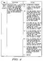
- FIG. 4illustrates one embodiment of the field definitions of control register 38 of FIG. 2 .
- each of fields 60 and 62are three-bit fields, where each field is capable of having 8 values (000, 001, 010, 011, 100, 101, 110, and 111).
- prefetch limit fields 60 and 62are used to control the prefetch algorithm used by the prefetch circuitry.
- prefetch limit fields 60 and 62define a limit on the maximum number of sequential prefetches which will be attempted between buffer misses for each corresponding master.
- Prefetch limit fields 60 and 62may also be used to define how many lines are prefetched each time.
- a value of 000indicates that no prefetching is performed between access requests from a corresponding master that result in misses in buffer 42 . That is, if master 12 prefetch limit field 60 is set to 000, then no prefetching occurs between misses in buffer 42 caused by access requests from master 12 . Similarly, if master 14 prefetch limit field 62 is set to 000, then no prefetching occurs between misses in buffer 42 caused by access requests from master 14 .
- a value of 001 for prefetch limit fields 60 and 62indicates that a single additional line (next sequential line in memory array 35 ) is prefetched on a buffer miss.
- a value of 010 for prefetch limit fields 60 and 62indicates that up to two additional lines may be prefetched following each buffer miss before prefetching is halted, where a single additional line (next sequential line in memory array 35 ) is prefetched on a buffer miss, and the next additional sequential line is prefetched on a buffer hit (if not already present).
- a value of 011 for prefetch limit fields 60 and 62indicates that up to three additional lines may be prefetched following each buffer miss before prefetching is halted. That is, for example, a single prefetch may be initiated after the initial miss, and a single additional prefetch may be initiated after each subsequent buffer hit (up to a total of three single prefetches).
- a value of 100 for prefetch limit fields 60 and 62indicates up to four additional lines may be prefetched following each buffer miss before prefetching is halted.
- a single prefetchmay be initiated after the initial miss, and a single additional prefetch may be initiated after each subsequent buffer hit (up to a total of four single prefetches).
- a value of 101 for prefetch limit fields 60 and 62indicates up to five additional lines may be prefetched following each buffer miss before prefetching is halted. That is, for example, a single prefetch may be initiated after the initial miss, and a single additional prefetch may be initiated after each subsequent buffer hit (up to a total of five single prefetches).
- a value of 110 for prefetch limit fields 60 and 62indicates an unlimited number of additional lines may be prefetched following each buffer miss. That is, for example, a single additional prefetch is initiated after each buffer hit or miss. (Note that in this embodiment, the value of 111 is reserved and is not being used to set a prefetch operation).
- control register 38may include more or less fields for each master utilizing more or less bits as needed.
- alternate definitions of prefetch limit fields 60 and 62may be applied as necessary to control prefetch circuitry 40 . The use and definition of prefetch limit fields will be further described in reference to FIG. 5 .
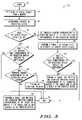
- FIG. 5illustrates, in flow diagram form, operation of data processing system 10 in accordance with one embodiment of the present invention.
- Flow 70begins with start 72 and proceeds to block 74 where an access request from a master, such as master 12 or master 14 , is received.
- a mastersuch as master 12 or master 14
- This access requestcan be many different types of access requests, such as a read request, a write request, a burst request, a non-burst request, a request for data, a request for instructions, etc. However, for ease of explanation herein, it will be assumed that the access request is a read request.
- the identity of the requesting masteris determined using, for example, a master identifier as provided by master identifier 26 of FIG. 1 .
- master identifier 26may have different master identifiers, for example, master 12 may have an identifier of 0 and master 14 may have an identifier of 1. Therefore, each master can be assigned a unique identifier. In an alternate embodiment, some masters may share a same identifier. Also, note that in alternate embodiments, which master is requesting the access may be determined in different ways rather than by providing a signal such as master identifier 26 .
- the correct prefetch counter and corresponding prefetch limitcan be selected from a plurality of prefetch counters and limits based upon the identity of the master identifier.
- decision diamond 96it is determined whether the prefetch limit corresponding to the requesting master indicates “No Prefetching”. If no prefetching is indicated, flow proceeds to ending oval 90 . Otherwise, if no prefetching is not indicated, flow then proceeds to decision diamond 80 , where it is determined whether the prefetch counter corresponding to the requesting master has expired. If the prefetch counter has not expired, flow then proceeds to block 82 . In block 82 , a single line prefetch is performed and the prefetch counter corresponding to the requesting master is decremented if the single line is not already in the prefetch buffer, thus keeping track of the number of prefetches that have occurred since the last miss. Flow then proceeds to ending oval 90 .
- the prefetch limitmay be used to limit the number of prefetches between buffer misses for a corresponding requesting master. Flow then proceeds to ending oval 90 .
- the prefetch counteris decremented by a fixed value, for example, 1, to indicate a prefetch was performed (e.g., in blocks 82 and 89 of FIG. 5 ).
- the prefetch counteris considered expired when the value of the prefetch counter reaches its lower limit, in this case 0.
- the initial value of the prefetch countermay be set to 0 (such as in block 86 of FIG. 5 ), and the prefetch counter may therefore be incremented by a fixed value, for example, 1, to indicate a prefetch was performed (such as in blocks 82 and 89 of FIG. 5 ).
- the prefetch counteris considered expired when the value of the counter reaches the corresponding prefetch limit.
- a predetermined number of linesmay be fetched during each prefetch (such as in blocks 82 and 89 of FIG. 5 ). That is, a predetermined number of lines may be prefetched in response to a hit, a miss, or both, if the lines are not already present in the prefetch buffer. Also, the corresponding prefetch counter may be decremented (or incremented) accordingly so as to keep track of the number of prefetches.
- prefetch limit fieldssuch as prefetch limit fields 60 and 62 in control register 38 may be used to define a prefetch of any predetermined number of lines after each miss or hit or both (until the corresponding counter expires) rather that just a single additional line.
- a prefetch countermay be used for each master, however, in an alternate embodiment, a single counter may be shared by multiple masters.
- a priority schememay be used where, for example, the priority scheme may be programmed by the user as to which master takes control of the single counter. For example, master 14 may require use of the counter that is currently being used by master 12 and if master 14 has priority over master 12 , then master 12 can relinquish control of the counter to master 14 . In this manner, multiple masters may share a single counter.
- the countermay be shared such that a prefetch limit may limit the number of prefetches between successive misses, regardless of the identity of the requesting master, rather than on a per master basis.
- the shared counterwould be set (such as in block 86 of FIG. 5 ) each time a miss occurs, regardless of the identity of the requesting master.
- decision diamond 80 and blocks 82 and 89 of FIG. 5would operate on this shared counter, regardless of the identity of the requesting master.
- multiple mastersmay share a prefetch limit in control register 38 .
- the prefetch limit fields of the CPU and DMAmay be set differently such that, for example, the DMA allows for a greater number of prefetches between misses as compared to the CPU.
- the prefetch limit fieldscan be programmed to take into account various differences between masters and to control the number of prefetches that occur between successive misses, as was described above. That is, after the prefetch limit is reached, no further prefetching occurs until the next buffer miss, since the likelihood that a sequential prefetch will be used decreases as the number of sequential prefetches increases. Also, it can be appreciated how the prefetch limit fields may be used to control the number of lines prefetch in response to each hit or miss or both (prior to the prefetch limit being reached) in order to further reduce wasted prefetches.
- the terms “comprises,” “comprising,” or any other variation thereof,are intended to cover a non-exclusive inclusion, such that a process, method, article, or apparatus that comprises a list of elements does not include only those elements but may include other elements not expressly listed or inherent to such process, method, article, or apparatus.
Landscapes
- Engineering & Computer Science (AREA)
- Theoretical Computer Science (AREA)
- Physics & Mathematics (AREA)
- General Engineering & Computer Science (AREA)
- General Physics & Mathematics (AREA)
- Memory System Of A Hierarchy Structure (AREA)
- Advance Control (AREA)
Abstract
Description
Claims (23)
Priority Applications (7)
| Application Number | Priority Date | Filing Date | Title |
|---|---|---|---|
| US10/631,136US7200719B2 (en) | 2003-07-31 | 2003-07-31 | Prefetch control in a data processing system |
| EP04778111AEP1652092A2 (en) | 2003-07-31 | 2004-07-13 | Prefetch control in a data processing system |
| CN2004800183628ACN100407165C (en) | 2003-07-31 | 2004-07-13 | Prefetch control in a data processing system |
| PCT/US2004/022438WO2005013039A2 (en) | 2003-07-31 | 2004-07-13 | Prefetch control in a data processing system |
| JP2006521871AJP4875981B2 (en) | 2003-07-31 | 2004-07-13 | Prefetch control in data processing system |
| KR1020067002041AKR101093317B1 (en) | 2003-07-31 | 2004-07-13 | Prefetch Control in Data Processing Systems |
| TW093123018ATWI352293B (en) | 2003-07-31 | 2004-07-30 | Data processing system and method for performing p |
Applications Claiming Priority (1)
| Application Number | Priority Date | Filing Date | Title |
|---|---|---|---|
| US10/631,136US7200719B2 (en) | 2003-07-31 | 2003-07-31 | Prefetch control in a data processing system |
Publications (2)
| Publication Number | Publication Date |
|---|---|
| US20060053256A1 US20060053256A1 (en) | 2006-03-09 |
| US7200719B2true US7200719B2 (en) | 2007-04-03 |
Family
ID=34115765
Family Applications (1)
| Application Number | Title | Priority Date | Filing Date |
|---|---|---|---|
| US10/631,136Expired - LifetimeUS7200719B2 (en) | 2003-07-31 | 2003-07-31 | Prefetch control in a data processing system |
Country Status (7)
| Country | Link |
|---|---|
| US (1) | US7200719B2 (en) |
| EP (1) | EP1652092A2 (en) |
| JP (1) | JP4875981B2 (en) |
| KR (1) | KR101093317B1 (en) |
| CN (1) | CN100407165C (en) |
| TW (1) | TWI352293B (en) |
| WO (1) | WO2005013039A2 (en) |
Cited By (2)
| Publication number | Priority date | Publication date | Assignee | Title |
|---|---|---|---|---|
| US7526604B1 (en)* | 2004-08-09 | 2009-04-28 | Nvidia Corporation | Command queueing speculative write prefetch |
| US20100153653A1 (en)* | 2008-12-15 | 2010-06-17 | Ahmed El-Mahdy | System and method for prefetching data |
Families Citing this family (17)
| Publication number | Priority date | Publication date | Assignee | Title |
|---|---|---|---|---|
| JP2006251923A (en)* | 2005-03-08 | 2006-09-21 | Oki Electric Ind Co Ltd | Look-ahead control method |
| US7346741B1 (en)* | 2005-05-10 | 2008-03-18 | Sun Microsystems, Inc. | Memory latency of processors with configurable stride based pre-fetching technique |
| CN101261610B (en)* | 2007-03-06 | 2014-04-02 | 西北农林科技大学 | Method and apparatus for multi-main apparatus non-violating access slave apparatus |
| JP4829191B2 (en)* | 2007-08-30 | 2011-12-07 | 株式会社東芝 | Cash system |
| US8473689B2 (en)* | 2010-07-27 | 2013-06-25 | Texas Instruments Incorporated | Predictive sequential prefetching for data caching |
| US8583894B2 (en)* | 2010-09-09 | 2013-11-12 | Advanced Micro Devices | Hybrid prefetch method and apparatus |
| CN102156633A (en)* | 2011-04-18 | 2011-08-17 | 北京北大众志微系统科技有限责任公司 | Preboot-execution-guided data prefetching method and system |
| US9342258B2 (en) | 2011-09-01 | 2016-05-17 | Freescale Semiconductor, Inc. | Integrated circuit device and method for providing data access control |
| US9645934B2 (en)* | 2013-09-13 | 2017-05-09 | Samsung Electronics Co., Ltd. | System-on-chip and address translation method thereof using a translation lookaside buffer and a prefetch buffer |
| US10942854B2 (en)* | 2018-05-09 | 2021-03-09 | Micron Technology, Inc. | Prefetch management for memory |
| US11010092B2 (en) | 2018-05-09 | 2021-05-18 | Micron Technology, Inc. | Prefetch signaling in memory system or sub-system |
| US10754578B2 (en) | 2018-05-09 | 2020-08-25 | Micron Technology, Inc. | Memory buffer management and bypass |
| US10714159B2 (en)* | 2018-05-09 | 2020-07-14 | Micron Technology, Inc. | Indication in memory system or sub-system of latency associated with performing an access command |
| US11294808B2 (en) | 2020-05-21 | 2022-04-05 | Micron Technology, Inc. | Adaptive cache |
| US11409657B2 (en) | 2020-07-14 | 2022-08-09 | Micron Technology, Inc. | Adaptive address tracking |
| US11422934B2 (en) | 2020-07-14 | 2022-08-23 | Micron Technology, Inc. | Adaptive address tracking |
| US20220091847A1 (en)* | 2020-09-23 | 2022-03-24 | Advanced Micro Devices, Inc. | Prefetching from indirect buffers at a processing unit |
Citations (8)
| Publication number | Priority date | Publication date | Assignee | Title |
|---|---|---|---|---|
| US5146578A (en) | 1989-05-01 | 1992-09-08 | Zenith Data Systems Corporation | Method of varying the amount of data prefetched to a cache memory in dependence on the history of data requests |
| US5410653A (en)* | 1992-06-16 | 1995-04-25 | International Business Machines Corporation | Asynchronous read-ahead disk caching using multiple disk I/O processes and dynamically variable prefetch length |
| US5619663A (en) | 1994-09-16 | 1997-04-08 | Philips Electronics North America Corp. | Computer instruction prefetch system |
| US6085291A (en) | 1995-11-06 | 2000-07-04 | International Business Machines Corporation | System and method for selectively controlling fetching and prefetching of data to a processor |
| US20030079089A1 (en) | 2001-10-18 | 2003-04-24 | International Business Machines Corporation | Programmable data prefetch pacing |
| US20040205299A1 (en)* | 2003-04-14 | 2004-10-14 | Bearden Brian S. | Method of triggering read cache pre-fetch to increase host read throughput |
| US20040221111A1 (en)* | 2003-04-30 | 2004-11-04 | Sun Microsystems, Inc. | Computer system including a memory controller configured to perform pre-fetch operations |
| US6901500B1 (en)* | 2000-07-28 | 2005-05-31 | Silicon Graphics, Inc. | Method and apparatus for prefetching information and storing the information in a stream buffer |
Family Cites Families (5)
| Publication number | Priority date | Publication date | Assignee | Title |
|---|---|---|---|---|
| US4709324A (en)* | 1985-11-27 | 1987-11-24 | Motorola, Inc. | Data processor control unit having an interrupt service using instruction prefetch redirection |
| JPH0754482B2 (en)* | 1990-08-07 | 1995-06-07 | 株式会社日立製作所 | Computer system |
| JP2720838B2 (en)* | 1995-06-19 | 1998-03-04 | 日本電気株式会社 | Data transfer device |
| US5802569A (en)* | 1996-04-22 | 1998-09-01 | International Business Machines Corp. | Computer system having cache prefetching amount based on CPU request types |
| US6832296B2 (en)* | 2002-04-09 | 2004-12-14 | Ip-First, Llc | Microprocessor with repeat prefetch instruction |
- 2003
- 2003-07-31USUS10/631,136patent/US7200719B2/ennot_activeExpired - Lifetime
- 2004
- 2004-07-13CNCN2004800183628Apatent/CN100407165C/ennot_activeExpired - Lifetime
- 2004-07-13JPJP2006521871Apatent/JP4875981B2/ennot_activeExpired - Lifetime
- 2004-07-13KRKR1020067002041Apatent/KR101093317B1/ennot_activeExpired - Lifetime
- 2004-07-13WOPCT/US2004/022438patent/WO2005013039A2/enactiveApplication Filing
- 2004-07-13EPEP04778111Apatent/EP1652092A2/ennot_activeWithdrawn
- 2004-07-30TWTW093123018Apatent/TWI352293B/ennot_activeIP Right Cessation
Patent Citations (8)
| Publication number | Priority date | Publication date | Assignee | Title |
|---|---|---|---|---|
| US5146578A (en) | 1989-05-01 | 1992-09-08 | Zenith Data Systems Corporation | Method of varying the amount of data prefetched to a cache memory in dependence on the history of data requests |
| US5410653A (en)* | 1992-06-16 | 1995-04-25 | International Business Machines Corporation | Asynchronous read-ahead disk caching using multiple disk I/O processes and dynamically variable prefetch length |
| US5619663A (en) | 1994-09-16 | 1997-04-08 | Philips Electronics North America Corp. | Computer instruction prefetch system |
| US6085291A (en) | 1995-11-06 | 2000-07-04 | International Business Machines Corporation | System and method for selectively controlling fetching and prefetching of data to a processor |
| US6901500B1 (en)* | 2000-07-28 | 2005-05-31 | Silicon Graphics, Inc. | Method and apparatus for prefetching information and storing the information in a stream buffer |
| US20030079089A1 (en) | 2001-10-18 | 2003-04-24 | International Business Machines Corporation | Programmable data prefetch pacing |
| US20040205299A1 (en)* | 2003-04-14 | 2004-10-14 | Bearden Brian S. | Method of triggering read cache pre-fetch to increase host read throughput |
| US20040221111A1 (en)* | 2003-04-30 | 2004-11-04 | Sun Microsystems, Inc. | Computer system including a memory controller configured to perform pre-fetch operations |
Non-Patent Citations (1)
| Title |
|---|
| Karkhanis, T.; "Saving Energy with Just In Time Instruction Delivery"; ISLPED '02; Aug. 12-14, 2002; pp. 178-183; USA. |
Cited By (5)
| Publication number | Priority date | Publication date | Assignee | Title |
|---|---|---|---|---|
| US7526604B1 (en)* | 2004-08-09 | 2009-04-28 | Nvidia Corporation | Command queueing speculative write prefetch |
| US20100153653A1 (en)* | 2008-12-15 | 2010-06-17 | Ahmed El-Mahdy | System and method for prefetching data |
| TWI453663B (en)* | 2008-12-15 | 2014-09-21 | Ibm | System and method for prefetching data |
| US9274965B2 (en) | 2008-12-15 | 2016-03-01 | International Business Machines Corporation | Prefetching data |
| US10810125B2 (en) | 2008-12-15 | 2020-10-20 | International Business Machines Corporation | Prefetching data |
Also Published As
| Publication number | Publication date |
|---|---|
| US20060053256A1 (en) | 2006-03-09 |
| KR20060052936A (en) | 2006-05-19 |
| KR101093317B1 (en) | 2011-12-14 |
| JP4875981B2 (en) | 2012-02-15 |
| CN1813246A (en) | 2006-08-02 |
| EP1652092A2 (en) | 2006-05-03 |
| TWI352293B (en) | 2011-11-11 |
| WO2005013039A2 (en) | 2005-02-10 |
| CN100407165C (en) | 2008-07-30 |
| WO2005013039A3 (en) | 2005-07-21 |
| JP2007500897A (en) | 2007-01-18 |
| TW200519604A (en) | 2005-06-16 |
Similar Documents
| Publication | Publication Date | Title |
|---|---|---|
| US7200719B2 (en) | Prefetch control in a data processing system | |
| US20230418759A1 (en) | Slot/sub-slot prefetch architecture for multiple memory requestors | |
| US8725987B2 (en) | Cache memory system including selectively accessible pre-fetch memory for pre-fetch of variable size data | |
| US6219760B1 (en) | Cache including a prefetch way for storing cache lines and configured to move a prefetched cache line to a non-prefetch way upon access to the prefetched cache line | |
| JP4064924B2 (en) | Method and apparatus for controlling memory access | |
| US20030033461A1 (en) | Data processing system having an adaptive priority controller | |
| JP5063104B2 (en) | Loss of ownership of cache entry over time of entry | |
| US7444435B2 (en) | Non-fenced list DMA command mechanism | |
| US6718439B1 (en) | Cache memory and method of operation | |
| US6871246B2 (en) | Prefetch control in a data processing system | |
| US20080201528A1 (en) | Memory access systems for configuring ways as cache or directly addressable memory | |
| US6976110B2 (en) | Method and apparatus for reducing interrupt latency by dynamic buffer sizing | |
| US6411218B1 (en) | Priority-encoding device selection using variable arbitrary rankings | |
| US7313658B2 (en) | Microprocessor and method for utilizing disparity between bus clock and core clock frequencies to prioritize cache line fill bus access requests | |
| JP5058116B2 (en) | DMAC issue mechanism by streaming ID method | |
| US10120819B2 (en) | System and method for cache memory line fill using interrupt indication | |
| JP4431492B2 (en) | Data transfer unit that supports multiple coherency granules | |
| JPH0644069A (en) | Microprocessor for controlling peripheral device |
Legal Events
| Date | Code | Title | Description |
|---|---|---|---|
| AS | Assignment | Owner name:MOTOROLA, INC., ILLINOIS Free format text:ASSIGNMENT OF ASSIGNORS INTEREST;ASSIGNORS:MOYER, WILLIAM C.;LEE, LEA HWANG;MALIK, AFZAL M.;REEL/FRAME:014366/0408 Effective date:20030731 | |
| AS | Assignment | Owner name:FREESCALE SEMICONDUCTOR, INC., TEXAS Free format text:ASSIGNMENT OF ASSIGNORS INTEREST;ASSIGNOR:MOTOROLA, INC;REEL/FRAME:015360/0718 Effective date:20040404 | |
| AS | Assignment | Owner name:CITIBANK, N.A. AS COLLATERAL AGENT, NEW YORK Free format text:SECURITY AGREEMENT;ASSIGNORS:FREESCALE SEMICONDUCTOR, INC.;FREESCALE ACQUISITION CORPORATION;FREESCALE ACQUISITION HOLDINGS CORP.;AND OTHERS;REEL/FRAME:018855/0129 Effective date:20061201 | |
| STCF | Information on status: patent grant | Free format text:PATENTED CASE | |
| CC | Certificate of correction | ||
| AS | Assignment | Owner name:CITIBANK, N.A., AS COLLATERAL AGENT, NEW YORK Free format text:SECURITY AGREEMENT;ASSIGNOR:FREESCALE SEMICONDUCTOR, INC.;REEL/FRAME:020045/0448 Effective date:20070718 | |
| AS | Assignment | Owner name:CITIBANK, N.A., AS COLLATERAL AGENT, NEW YORK Free format text:SECURITY AGREEMENT;ASSIGNOR:FREESCALE SEMICONDUCTOR, INC.;REEL/FRAME:024397/0001 Effective date:20100413 | |
| FPAY | Fee payment | Year of fee payment:4 | |
| AS | Assignment | Owner name:CITIBANK, N.A., AS NOTES COLLATERAL AGENT, NEW YORK Free format text:SECURITY AGREEMENT;ASSIGNOR:FREESCALE SEMICONDUCTOR, INC.;REEL/FRAME:030633/0424 Effective date:20130521 Owner name:CITIBANK, N.A., AS NOTES COLLATERAL AGENT, NEW YOR Free format text:SECURITY AGREEMENT;ASSIGNOR:FREESCALE SEMICONDUCTOR, INC.;REEL/FRAME:030633/0424 Effective date:20130521 | |
| AS | Assignment | Owner name:CITIBANK, N.A., AS NOTES COLLATERAL AGENT, NEW YORK Free format text:SECURITY AGREEMENT;ASSIGNOR:FREESCALE SEMICONDUCTOR, INC.;REEL/FRAME:031591/0266 Effective date:20131101 Owner name:CITIBANK, N.A., AS NOTES COLLATERAL AGENT, NEW YOR Free format text:SECURITY AGREEMENT;ASSIGNOR:FREESCALE SEMICONDUCTOR, INC.;REEL/FRAME:031591/0266 Effective date:20131101 | |
| FPAY | Fee payment | Year of fee payment:8 | |
| AS | Assignment | Owner name:FREESCALE SEMICONDUCTOR, INC., TEXAS Free format text:PATENT RELEASE;ASSIGNOR:CITIBANK, N.A., AS COLLATERAL AGENT;REEL/FRAME:037354/0655 Effective date:20151207 Owner name:FREESCALE SEMICONDUCTOR, INC., TEXAS Free format text:PATENT RELEASE;ASSIGNOR:CITIBANK, N.A., AS COLLATERAL AGENT;REEL/FRAME:037354/0225 Effective date:20151207 Owner name:FREESCALE SEMICONDUCTOR, INC., TEXAS Free format text:PATENT RELEASE;ASSIGNOR:CITIBANK, N.A., AS COLLATERAL AGENT;REEL/FRAME:037356/0143 Effective date:20151207 Owner name:FREESCALE SEMICONDUCTOR, INC., TEXAS Free format text:PATENT RELEASE;ASSIGNOR:CITIBANK, N.A., AS COLLATERAL AGENT;REEL/FRAME:037356/0553 Effective date:20151207 | |
| AS | Assignment | Owner name:MORGAN STANLEY SENIOR FUNDING, INC., MARYLAND Free format text:ASSIGNMENT AND ASSUMPTION OF SECURITY INTEREST IN PATENTS;ASSIGNOR:CITIBANK, N.A.;REEL/FRAME:037486/0517 Effective date:20151207 | |
| AS | Assignment | Owner name:MORGAN STANLEY SENIOR FUNDING, INC., MARYLAND Free format text:ASSIGNMENT AND ASSUMPTION OF SECURITY INTEREST IN PATENTS;ASSIGNOR:CITIBANK, N.A.;REEL/FRAME:037518/0292 Effective date:20151207 | |
| AS | Assignment | Owner name:MORGAN STANLEY SENIOR FUNDING, INC., MARYLAND Free format text:SUPPLEMENT TO THE SECURITY AGREEMENT;ASSIGNOR:FREESCALE SEMICONDUCTOR, INC.;REEL/FRAME:039138/0001 Effective date:20160525 | |
| AS | Assignment | Owner name:NXP, B.V., F/K/A FREESCALE SEMICONDUCTOR, INC., NETHERLANDS Free format text:RELEASE BY SECURED PARTY;ASSIGNOR:MORGAN STANLEY SENIOR FUNDING, INC.;REEL/FRAME:040925/0001 Effective date:20160912 Owner name:NXP, B.V., F/K/A FREESCALE SEMICONDUCTOR, INC., NE Free format text:RELEASE BY SECURED PARTY;ASSIGNOR:MORGAN STANLEY SENIOR FUNDING, INC.;REEL/FRAME:040925/0001 Effective date:20160912 | |
| AS | Assignment | Owner name:NXP B.V., NETHERLANDS Free format text:RELEASE BY SECURED PARTY;ASSIGNOR:MORGAN STANLEY SENIOR FUNDING, INC.;REEL/FRAME:040928/0001 Effective date:20160622 | |
| AS | Assignment | Owner name:NXP USA, INC., TEXAS Free format text:CHANGE OF NAME;ASSIGNOR:FREESCALE SEMICONDUCTOR INC.;REEL/FRAME:040652/0180 Effective date:20161107 | |
| AS | Assignment | Owner name:NXP USA, INC., TEXAS Free format text:CORRECTIVE ASSIGNMENT TO CORRECT THE NATURE OF CONVEYANCE LISTED CHANGE OF NAME SHOULD BE MERGER AND CHANGE PREVIOUSLY RECORDED AT REEL: 040652 FRAME: 0180. ASSIGNOR(S) HEREBY CONFIRMS THE MERGER AND CHANGE OF NAME;ASSIGNOR:FREESCALE SEMICONDUCTOR INC.;REEL/FRAME:041354/0148 Effective date:20161107 | |
| AS | Assignment | Owner name:MORGAN STANLEY SENIOR FUNDING, INC., MARYLAND Free format text:CORRECTIVE ASSIGNMENT TO CORRECT THE REMOVE PATENTS 8108266 AND 8062324 AND REPLACE THEM WITH 6108266 AND 8060324 PREVIOUSLY RECORDED ON REEL 037518 FRAME 0292. ASSIGNOR(S) HEREBY CONFIRMS THE ASSIGNMENT AND ASSUMPTION OF SECURITY INTEREST IN PATENTS;ASSIGNOR:CITIBANK, N.A.;REEL/FRAME:041703/0536 Effective date:20151207 | |
| MAFP | Maintenance fee payment | Free format text:PAYMENT OF MAINTENANCE FEE, 12TH YEAR, LARGE ENTITY (ORIGINAL EVENT CODE: M1553); ENTITY STATUS OF PATENT OWNER: LARGE ENTITY Year of fee payment:12 | |
| AS | Assignment | Owner name:SHENZHEN XINGUODU TECHNOLOGY CO., LTD., CHINA Free format text:CORRECTIVE ASSIGNMENT TO CORRECT THE TO CORRECT THE APPLICATION NO. FROM 13,883,290 TO 13,833,290 PREVIOUSLY RECORDED ON REEL 041703 FRAME 0536. ASSIGNOR(S) HEREBY CONFIRMS THE THE ASSIGNMENT AND ASSUMPTION OF SECURITYINTEREST IN PATENTS.;ASSIGNOR:MORGAN STANLEY SENIOR FUNDING, INC.;REEL/FRAME:048734/0001 Effective date:20190217 | |
| AS | Assignment | Owner name:NXP B.V., NETHERLANDS Free format text:RELEASE BY SECURED PARTY;ASSIGNOR:MORGAN STANLEY SENIOR FUNDING, INC.;REEL/FRAME:050744/0097 Effective date:20190903 | |
| AS | Assignment | Owner name:MORGAN STANLEY SENIOR FUNDING, INC., MARYLAND Free format text:CORRECTIVE ASSIGNMENT TO CORRECT THE REMOVE APPLICATION11759915 AND REPLACE IT WITH APPLICATION 11759935 PREVIOUSLY RECORDED ON REEL 037486 FRAME 0517. ASSIGNOR(S) HEREBY CONFIRMS THE ASSIGNMENT AND ASSUMPTION OF SECURITYINTEREST IN PATENTS;ASSIGNOR:CITIBANK, N.A.;REEL/FRAME:053547/0421 Effective date:20151207 | |
| AS | Assignment | Owner name:NXP B.V., NETHERLANDS Free format text:CORRECTIVE ASSIGNMENT TO CORRECT THE REMOVEAPPLICATION 11759915 AND REPLACE IT WITH APPLICATION11759935 PREVIOUSLY RECORDED ON REEL 040928 FRAME 0001. ASSIGNOR(S) HEREBY CONFIRMS THE RELEASE OF SECURITYINTEREST;ASSIGNOR:MORGAN STANLEY SENIOR FUNDING, INC.;REEL/FRAME:052915/0001 Effective date:20160622 | |
| AS | Assignment | Owner name:NXP, B.V. F/K/A FREESCALE SEMICONDUCTOR, INC., NETHERLANDS Free format text:CORRECTIVE ASSIGNMENT TO CORRECT THE REMOVEAPPLICATION 11759915 AND REPLACE IT WITH APPLICATION11759935 PREVIOUSLY RECORDED ON REEL 040925 FRAME 0001. ASSIGNOR(S) HEREBY CONFIRMS THE RELEASE OF SECURITYINTEREST;ASSIGNOR:MORGAN STANLEY SENIOR FUNDING, INC.;REEL/FRAME:052917/0001 Effective date:20160912 |