US7200021B2 - Stacked DRAM memory chip for a dual inline memory module (DIMM) - Google Patents
Stacked DRAM memory chip for a dual inline memory module (DIMM)Download PDFInfo
- Publication number
- US7200021B2 US7200021B2US11/010,942US1094204AUS7200021B2US 7200021 B2US7200021 B2US 7200021B2US 1094204 AUS1094204 AUS 1094204AUS 7200021 B2US7200021 B2US 7200021B2
- Authority
- US
- United States
- Prior art keywords
- memory
- dram memory
- stacked dram
- stacked
- internal
- Prior art date
- Legal status (The legal status is an assumption and is not a legal conclusion. Google has not performed a legal analysis and makes no representation as to the accuracy of the status listed.)
- Expired - Lifetime
Links
Images


Classifications
- G—PHYSICS
- G11—INFORMATION STORAGE
- G11C—STATIC STORES
- G11C5/00—Details of stores covered by group G11C11/00
- G11C5/02—Disposition of storage elements, e.g. in the form of a matrix array
- G11C5/04—Supports for storage elements, e.g. memory modules; Mounting or fixing of storage elements on such supports
- B—PERFORMING OPERATIONS; TRANSPORTING
- B82—NANOTECHNOLOGY
- B82Y—SPECIFIC USES OR APPLICATIONS OF NANOSTRUCTURES; MEASUREMENT OR ANALYSIS OF NANOSTRUCTURES; MANUFACTURE OR TREATMENT OF NANOSTRUCTURES
- B82Y10/00—Nanotechnology for information processing, storage or transmission, e.g. quantum computing or single electron logic
- H—ELECTRICITY
- H01—ELECTRIC ELEMENTS
- H01L—SEMICONDUCTOR DEVICES NOT COVERED BY CLASS H10
- H01L25/00—Assemblies consisting of a plurality of semiconductor or other solid state devices
- H01L25/03—Assemblies consisting of a plurality of semiconductor or other solid state devices all the devices being of a type provided for in a single subclass of subclasses H10B, H10D, H10F, H10H, H10K or H10N, e.g. assemblies of rectifier diodes
- H01L25/04—Assemblies consisting of a plurality of semiconductor or other solid state devices all the devices being of a type provided for in a single subclass of subclasses H10B, H10D, H10F, H10H, H10K or H10N, e.g. assemblies of rectifier diodes the devices not having separate containers
- H01L25/065—Assemblies consisting of a plurality of semiconductor or other solid state devices all the devices being of a type provided for in a single subclass of subclasses H10B, H10D, H10F, H10H, H10K or H10N, e.g. assemblies of rectifier diodes the devices not having separate containers the devices being of a type provided for in group H10D89/00
- H01L25/0657—Stacked arrangements of devices
- H—ELECTRICITY
- H01—ELECTRIC ELEMENTS
- H01L—SEMICONDUCTOR DEVICES NOT COVERED BY CLASS H10
- H01L25/00—Assemblies consisting of a plurality of semiconductor or other solid state devices
- H01L25/18—Assemblies consisting of a plurality of semiconductor or other solid state devices the devices being of the types provided for in two or more different main groups of the same subclass of H10B, H10D, H10F, H10H, H10K or H10N
- H—ELECTRICITY
- H01—ELECTRIC ELEMENTS
- H01L—SEMICONDUCTOR DEVICES NOT COVERED BY CLASS H10
- H01L2224/00—Indexing scheme for arrangements for connecting or disconnecting semiconductor or solid-state bodies and methods related thereto as covered by H01L24/00
- H01L2224/01—Means for bonding being attached to, or being formed on, the surface to be connected, e.g. chip-to-package, die-attach, "first-level" interconnects; Manufacturing methods related thereto
- H01L2224/42—Wire connectors; Manufacturing methods related thereto
- H01L2224/47—Structure, shape, material or disposition of the wire connectors after the connecting process
- H01L2224/48—Structure, shape, material or disposition of the wire connectors after the connecting process of an individual wire connector
- H01L2224/4805—Shape
- H01L2224/4809—Loop shape
- H01L2224/48091—Arched
- H—ELECTRICITY
- H01—ELECTRIC ELEMENTS
- H01L—SEMICONDUCTOR DEVICES NOT COVERED BY CLASS H10
- H01L2224/00—Indexing scheme for arrangements for connecting or disconnecting semiconductor or solid-state bodies and methods related thereto as covered by H01L24/00
- H01L2224/01—Means for bonding being attached to, or being formed on, the surface to be connected, e.g. chip-to-package, die-attach, "first-level" interconnects; Manufacturing methods related thereto
- H01L2224/42—Wire connectors; Manufacturing methods related thereto
- H01L2224/47—Structure, shape, material or disposition of the wire connectors after the connecting process
- H01L2224/48—Structure, shape, material or disposition of the wire connectors after the connecting process of an individual wire connector
- H01L2224/481—Disposition
- H01L2224/48151—Connecting between a semiconductor or solid-state body and an item not being a semiconductor or solid-state body, e.g. chip-to-substrate, chip-to-passive
- H01L2224/48221—Connecting between a semiconductor or solid-state body and an item not being a semiconductor or solid-state body, e.g. chip-to-substrate, chip-to-passive the body and the item being stacked
- H01L2224/48225—Connecting between a semiconductor or solid-state body and an item not being a semiconductor or solid-state body, e.g. chip-to-substrate, chip-to-passive the body and the item being stacked the item being non-metallic, e.g. insulating substrate with or without metallisation
- H01L2224/48227—Connecting between a semiconductor or solid-state body and an item not being a semiconductor or solid-state body, e.g. chip-to-substrate, chip-to-passive the body and the item being stacked the item being non-metallic, e.g. insulating substrate with or without metallisation connecting the wire to a bond pad of the item
- H—ELECTRICITY
- H01—ELECTRIC ELEMENTS
- H01L—SEMICONDUCTOR DEVICES NOT COVERED BY CLASS H10
- H01L2225/00—Details relating to assemblies covered by the group H01L25/00 but not provided for in its subgroups
- H01L2225/03—All the devices being of a type provided for in the same main group of the same subclass of class H10, e.g. assemblies of rectifier diodes
- H01L2225/04—All the devices being of a type provided for in the same main group of the same subclass of class H10, e.g. assemblies of rectifier diodes the devices not having separate containers
- H01L2225/065—All the devices being of a type provided for in the same main group of the same subclass of class H10
- H01L2225/06503—Stacked arrangements of devices
- H01L2225/0651—Wire or wire-like electrical connections from device to substrate
- H—ELECTRICITY
- H01—ELECTRIC ELEMENTS
- H01L—SEMICONDUCTOR DEVICES NOT COVERED BY CLASS H10
- H01L2225/00—Details relating to assemblies covered by the group H01L25/00 but not provided for in its subgroups
- H01L2225/03—All the devices being of a type provided for in the same main group of the same subclass of class H10, e.g. assemblies of rectifier diodes
- H01L2225/04—All the devices being of a type provided for in the same main group of the same subclass of class H10, e.g. assemblies of rectifier diodes the devices not having separate containers
- H01L2225/065—All the devices being of a type provided for in the same main group of the same subclass of class H10
- H01L2225/06503—Stacked arrangements of devices
- H01L2225/06524—Electrical connections formed on device or on substrate, e.g. a deposited or grown layer
- H—ELECTRICITY
- H01—ELECTRIC ELEMENTS
- H01L—SEMICONDUCTOR DEVICES NOT COVERED BY CLASS H10
- H01L2225/00—Details relating to assemblies covered by the group H01L25/00 but not provided for in its subgroups
- H01L2225/03—All the devices being of a type provided for in the same main group of the same subclass of class H10, e.g. assemblies of rectifier diodes
- H01L2225/04—All the devices being of a type provided for in the same main group of the same subclass of class H10, e.g. assemblies of rectifier diodes the devices not having separate containers
- H01L2225/065—All the devices being of a type provided for in the same main group of the same subclass of class H10
- H01L2225/06503—Stacked arrangements of devices
- H01L2225/06527—Special adaptation of electrical connections, e.g. rewiring, engineering changes, pressure contacts, layout
- H—ELECTRICITY
- H01—ELECTRIC ELEMENTS
- H01L—SEMICONDUCTOR DEVICES NOT COVERED BY CLASS H10
- H01L2924/00—Indexing scheme for arrangements or methods for connecting or disconnecting semiconductor or solid-state bodies as covered by H01L24/00
- H01L2924/01—Chemical elements
- H01L2924/0102—Calcium [Ca]
- H—ELECTRICITY
- H01—ELECTRIC ELEMENTS
- H01L—SEMICONDUCTOR DEVICES NOT COVERED BY CLASS H10
- H01L2924/00—Indexing scheme for arrangements or methods for connecting or disconnecting semiconductor or solid-state bodies as covered by H01L24/00
- H01L2924/01—Chemical elements
- H01L2924/01068—Erbium [Er]
- H—ELECTRICITY
- H01—ELECTRIC ELEMENTS
- H01L—SEMICONDUCTOR DEVICES NOT COVERED BY CLASS H10
- H01L2924/00—Indexing scheme for arrangements or methods for connecting or disconnecting semiconductor or solid-state bodies as covered by H01L24/00
- H01L2924/01—Chemical elements
- H01L2924/01078—Platinum [Pt]
- H—ELECTRICITY
- H01—ELECTRIC ELEMENTS
- H01L—SEMICONDUCTOR DEVICES NOT COVERED BY CLASS H10
- H01L2924/00—Indexing scheme for arrangements or methods for connecting or disconnecting semiconductor or solid-state bodies as covered by H01L24/00
- H01L2924/15—Details of package parts other than the semiconductor or other solid state devices to be connected
- H01L2924/151—Die mounting substrate
- H01L2924/153—Connection portion
- H01L2924/1531—Connection portion the connection portion being formed only on the surface of the substrate opposite to the die mounting surface
- H01L2924/15311—Connection portion the connection portion being formed only on the surface of the substrate opposite to the die mounting surface being a ball array, e.g. BGA
Definitions
- the inventionrelates in general to a DRAM chip for a DRAM Dual Inline Memory Module (DIMM) and in particular to a DRAM memory chip for a registered Dual Inline Memory Module (DIMM).
- DIMMDual Inline Memory Module
- SIMMsingle inline memory modules
- PCBprinted circuit board
- PS/2PS/2
- SIMM modulesDue to the different data bus width of the memory module in some processors, sometimes several SIMM modules are installed in pairs to fill a memory bank. For instance, in 80386 or 80486 systems having a data bus width of 32 bits either four 30 pins SIMMs or one 72 pin SIMM are required for one memory bank. For pentium systems having a data bus width of 64 bits two 72 pin SIMMs are required.
- SIMMsingle inline memory module
- the RAM technologies used by single inline memory modulesinclude EDO and FPM.
- DIMMDual Inline Memory Modules
- SIMMsingle inline memory modules
- SIMMSsingle inline memory modules
- DIMMSdual inline memory modules
- Dual Inline Memory ModulesThere are different types of Dual Inline Memory Modules (DIMM). An unbuffered Dual Inline Memory Module does not contain buffers or registers located on the module. These unbuffered Dual Inline Memory Modules are typically used in desktop PC systems and workstations. The number of pins are typically 168 in single data rate (SDR) memory modules, 184 pins in double data rate modules and in DDR-2 modules.
- DDR-2-DRAMsare a natural extension of the existing DDR-DRAMs. DDR-2 has been introduced at an operation frequency of 200 MHz and is going to be extended to 266 MHz (DDR-2 533), 333 MHz (DDR-2 667) for the main memory and even 400 MHz (DDR-2 800) for special applications.
- DDR-SDRAMsynchronous DRAMs
- Dual Inline Memory Moduleis a registered Dual Inline Memory Module.
- a registered Dual Inline Memory Modulecomprises several additional circuits on the module in particular a redriver buffer component like a register to redrive command address signals. Further, a phase locked loop (PLL) is provided for timing alignments to redrive clock signals.
- PLLphase locked loop
- Registered Dual Inline Memory Modulesare typically used in highend servers and highend workstations.
- ECC-Dual Inline Memory Modulescomprise error correction bits or ECC bits.
- This type of Dual Inline Memory Modulehas a total of 64 data bits plus 8 ECC bits and is used mostly for server computers.
- Registered Dual Inline Memory Modules either with ECC or without ECCare used for SDR, DDR and DDR-2.
- Dual Inline Memory Modulesare so called small outline DIMM (SO-DIMM). They are an enhanced version of standard Dual Inline Memory Modules and are used in laptops and in some special servers.
- SO-DIMMsmall outline DIMM
- a Dual Inline Memory Modulecomprises a predetermined number N of memory chips (DRAMs) on its printed circuit board.
- the data width of each memory chipis typically 4 bits, 8 bits or 16 bits.
- DIMMmemory chips
- personal computermostly uses a unbuffered Dual Inline Memory Module if a DIMM is selected as the main memory.
- registered Dual Inline Memory Modulesare the popular choice.
- DRAMsmemory chips
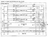
- FIG. 1shows a Dual Inline Memory Module according to the state of the art.
- the Dual Inline Memory Modulecomprises N DRAM chips mounted on the upper side of the printed circuit board (PCB).
- the registered Dual Inline Memory Module as shown in FIG. 1comprises a command and address buffer which buffers command and address signals applied to the Dual Inline Memory Module by a main motherboard and which outputs these signals via a command and address bus (CA) to the DRAM chips mounted on the printed circuit board.
- a chip selection signal Sis also buffered for selecting the desired DRAM chip mounted on the DIMM circuit board.
- All DRAM chipsare clocked by a clock signal CLK′_ which is buffered by a clock signal buffer which is also mounted on the Dual Inline Memory Module (DIMM).
- Each DRAM chipis connected to the motherboard by a separate databus (DQ) having q data lines.
- the data bus of each DRAM chipcomprises typically 4 to 16 bits.
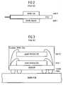
- FIG. 2shows a cross section of the Dual Inline Memory Module (DIMM) as shown in FIG. 1 along the line A–A′.
- DIMMDual Inline Memory Module
- the DIMMhas DRAM chips mounted on both sides of the printed circuit board (PCB).
- PCBprinted circuit board
- the DRAM Dual Inline Memory Module as shown in FIG. 2comprises two memory ranks or memory levels, i.e. memory rank 0 and memory rank 1.
- DIMMDual Inline Memory Module
- FIG. 3shows a stacked DRAM chip having an upper memory die and a lower memory die thus providing two memory ranks within one stacked DRAM chip.
- the two memory diesare packaged within one chip on a substrate.
- the stacked DRAM chipis connected to the printed circuit board via pads such as solder balls.
- Dual Inline Memory Moduleswhich have stacked DRAM chips as shown in FIG. 3 on both sides of the printed circuit board have four memory ranks, i.e. two memory ranks on the top side and two memory ranks on the bottom side.
- Dual Inline Memory Modules having two memory ranksare allowed.
- the load on the DQ bus and the CA bus as shown in FIG. 1is increased.
- the increase of loadis not dramatically since the command and address bus (CA) is running at half speed in comparison to the data bus and the command and address buffer redrives the address and command signals applied by the processor on the motherboard to the Dual Inline Memory Module.
- the increase of memory ranks on the Dual Inline Memory Modulehowever causes an increase of the load of the DQ-data bus which is driven by the controller on the motherboard.
- the data rate on the DQ-bussesis very high in particular when running at DDR-2 data rate.
- the redriving unitfurther comprises a memory rank decoder for generating the internal memory rank signal in response to external select signals applied to control pads of the DRAM memory chip.
- the memory rank decodercontrols the multiplexer/demultiplexer.
- the multiplexer/demultiplexercomprises buffers for buffering the data signals transmitted via the switched data lines.
- all DRAM memory diesare clocked by a common internal clock signal.
- the redriving unitfurther comprises a buffer for driving an external clock signal applied to a clock pad of the DRAM memory chip to generate said internal clock signal.
- the stack of DRAM dies and the redriving unitare integrated in the DRAM memory chip.
- the redriving unitis powered via power supply pads of said DRAM memory chip.
- the inventionfurther provides a Dual Inline Memory Module comprising a plurality of stacked DRAM memory chips, wherein each stacked DRAM memory chip has
- the Dual Inline Memory Modulecomprises a command and address buffer chip for buffering command and address signals received from the main printed circuit board.
- the command and address bufferis connected via a command and address bus to all stacked DRAM memory chips mounted on a printed circuit board of said Dual Inline Memory Module.
- FIG. 1shows a Dual Inline Memory Module (DIMM) according to the state of the art from above;
- DIMMDual Inline Memory Module
- FIG. 2is a cross section view of the Dual Inline Memory Module according to the state of the art as shown in FIG. 1 ;
- FIG. 3shows a cross section of a stacked DRAM chip according to the state of the art
- FIG. 4shows a cross section view of a preferred embodiment of a stacked DRAM chip according to the present invention.
- FIG. 5shows a top view of a Dual Inline Memory Module comprising stacked DRAM chips according to the present invention.
- FIG. 4it shows a cross section of a stacked DRAM memory chip 1 mounted on a printed circuit board (PCB) 2 of a Dual Inline Memory Module 3 (shown in FIG. 5 ).
- the stacked DRAM chip I as shown in FIG. 4comprises in the shown embodiment four stacked DRAM memory dies 4 - 0 , 4 - 1 , 4 - 2 , 4 - 3 .
- Each memory die 4 - iis selectable by a corresponding memory rank signal r–i.
- the DRAM memory dies 4 - iinclude an array of memory cells (designated 24 - 0 . 24 - 1 . 24 - 2 . and 24 - 3 ) which are addressable by address lines.
- a common internal address bus 5comprises a predetermined number of internal address lines 5 - i provided for addressing memory cells 24 - i of the memory dies 4 - i .
- FIG. 4shows as an example an address pad A 0 connected via an address line 5 - i to all memory dies 4 - i . All address lines of the internal address bus are connected in parallel to all four DRAM memory dies of the stacked DRAM chip 1 .
- the memory dies 4 - iare clocked by a clock signal CLK applied to all memory dies via an internal clock line 6 as shown in FIG. 4 .
- Each memory die 4 - iis connected via a corresponding internal data bus 7 - i to a DQ multiplexer/demultiplexer BA.
- Each internal data bus 7 - icomprises a predetermined number of data lines (i.e., 7 - 0 . 7 - 1 , 7 - 2 . and 7 - 3 ) for connecting the respective memory die 4 - i to the DQ-multiplexer/demultiplexer BA.
- Each DQ-data bus 7 - icomprises for instance 4 to 16 bit lines.
- the internal data busses DQ-busses 7 - iare provided for writing data into the memory cells and for reading data out of memory cells 24 - i of the stacked DRAM memory dies 4 - i.
- the stacked DRAM chip 1according to the present invention as shown in FIG. 4 comprises beneath the stacked DRAM memory dies 4 - i a redriving unit 8 .
- the redriving unit 8comprises the DQ-multiplexer/demultiplexer unit 8 A and buffers 8 B for all internal address lines 5 - i provided for driving external address signals applied to address pads 9 - i of said DRAM memory chip 1 .
- the redriving unit 8further comprises a buffer 8 C for driving a clock signal CLK applied to the DRAM chip 1 by means of a clock signal pad 10 .
- the redriving unit 8comprises in all embodiments the multiplexer/demultiplexer 8 A which switches the internal data lines or data bus 7 - i of a selected DRAM memory die to data pads 11 of the DRAM memory chip 1 .
- Pads 9 , 10 , 11are formed by balls or pins.
- the number q of DQ lines per DRAM chip Iis in a preferred embodiment either four or eight.
- Redriving unit 8is power by power supply pads 25 of DRAM memory chip 1 .
- the redriving unit 8further comprises a memory rank decoder 8 D for generating internal memory rank selection signals r–i in response to external select signals S i applied to control pads 12 - 0 , 12 - 1 of the DRAM memory chip 1 as shown in FIG. 4 .
- the memory rank decoder 8 Dreceives in the shown embodiment two external selection signals S 0 , S 1 and decodes them to generate four memory rank signals r i which are applied to the memory dies 4 - i via control lines 13 - i.
- the memory rank decoder 8 Dis integrated within the redriving unit 8 of the stacked DRAM 1 .
- the decoder 8 Dis integrated in central command and address buffer of the Dual Inline Memory Module 3 . Integration of the memory rank decoder 8 D within the redriving unit 8 has the advantage that the number of selection signals and selection lines on the Dual Inline Memory Module 3 can be minimized.
- the memory rank decoder 8 Dcontrols the DQ-multiplexer/demultiplexer 8 A via internal control lines 14 .
- the multiplexer/demultiplexer 8 Acomprises in a preferred embodiment buffers 8 E for driving the data signals transmitted via the switched data lines.
- the multiplexer/demultiplexer 8 Ais switched from the multiplexing mode (read mode) to the demultiplexing mode (write mode) in response to a write Enable (WE) control signal.
- the stack of DRAM memory dies 4 - i and the redriving unit 8are integrated in the DRAM memory chip 1 .
- the memory diesare integrated in a preferred embodiment into a FBGA (fine pitch ball grid).
- FBGAfine pitch ball grid
- the provision of a redriving unit 8 within the stacked DRAM chip 1 which might be integrated in the FBGA packageallows to increase the number of memory dies 4 - i without increasing the load for the command and address buffer 15 and more importantly the load for the processor on the main board. This allows a significantly higher operation frequency for operating the Dual Inline Memory Module 3 .
- the redriving unit 8is provided beneath the memory die stack on the bottom side of the stacked DRAM chip 1 .
- FIG. 5shows a Dual Inline Memory Module 3 comprising a predetermined number N of stacked DRAM chips I as shown in FIG. 4 .
- the number N of DRAMsis typically 9 or 18 depending on the number M of memory ranks.
- Each stacked DRAM chip Icomprises M stacked DRAM memory dies.
- the number M of stacked DRAM memory diesmay be 1, 2, 4, 8,16 . . . DRAM memory dies.
- the Dual Inline Memory Module 3further comprises at least one central command and address buffer 15 which is located in the middle of the printed circuit board 2 (shown in FIG. 4 ) of the Dual Inline Memory Module 3 .
- the command and address buffer 15is connected via a command and address bus 16 to all DRAM memory chips 1 on the Dual Inline Memory Module 3 .
- the command and address buffer 15receives command and address signals from the main circuit board via command and address lines 17 and drives them via the command and address bus 16 to all DRAM chips 1 .
- the command and address buffer 15further receives selection signals via a selection control bus 18 and drives them via a selection signal bus 19 to all DRAM chips 1 .
- the selection signals applied to the DRAM chips 1 via the selection bus 19selects the DRAM chip and the memory die 4 - i within the DRAM chip 1 .
- Mis the number of stacked memory dies or ranks within each DRAM chip 1 .
- the Dual Inline Memory Module 3according to the present invention as shown in FIG. 5 further comprises at least one contact pad 20 which is connected via a clock line 21 to a clock signal buffer 22 .
- the external clock signal received from the motherboardis buffered by the clock signal buffer 21 and applied to all DRAM memory chips 1 via an internal clock line 23 .
- Each DRAM chip 1comprises a redriving unit 8 with a buffer 8 C (shown in FIG. 4 ) for buffering the received internal clock signal.
- the Dual Inline Memory Module 3can be achieved with a very high memory density without increasing the load for the processor on the motherboard. Accordingly the Dual Inline Memory Module 3 comprising the stacked DRAM memory chips 1 according to the present invention allows higher operation frequencies of the processor.
- the stacking of the memory diesprovides unprecedented memory density per board area and offers at the same time superior electrical properties of the resulting dual inline memory component.
- a Dual Inline Memory Module 3 according to the present inventionis fully compatible with existing slots for Dual Inline Memories. Since the same interconnection technology is used for the stacked memory dies 4 - 1 these dies have similar electrical parameters.
- the DRAM memory chips 1are integrated in fine pitched ball grid packages (FPBG) in BOC board on chip technology.
- FPBGfine pitched ball grid packages
Landscapes
- Engineering & Computer Science (AREA)
- Microelectronics & Electronic Packaging (AREA)
- Power Engineering (AREA)
- Physics & Mathematics (AREA)
- General Physics & Mathematics (AREA)
- Nanotechnology (AREA)
- Chemical & Material Sciences (AREA)
- Condensed Matter Physics & Semiconductors (AREA)
- Computer Hardware Design (AREA)
- Crystallography & Structural Chemistry (AREA)
- Theoretical Computer Science (AREA)
- Mathematical Physics (AREA)
- Dram (AREA)
Abstract
Description
- (a) a predetermined number (M) of stacked DRAM memory dies;
- (b) wherein each DRAM memory die is selectable by a corresponding memory rank signal (r);
- (c) wherein each DRAM memory die comprises an array of memory cells;
- (d) wherein a common internal address bus consisting of address lines is provided for addressing the memory cells and is connected to all M stacked DRAM memory dies;
- (e) wherein M internal data buses consisting of internal data lines are provided for writing data into the memory cells and reading data out of the memory cells of the stacked DRAM memory dies;
wherein - (f) an integrated redriving unit is provided which comprises:
- (f1) buffers for all internal address lines provided for driving external address signals applied to address pads of said DRAM memory chip and;
- (f2) a multiplexer/demultiplexer which switches the internal data lines of the selected DRAM memory die to data pads of said DRAM memory chip.
- (a) a predetermined number (M) of stacked DRAM memory dies;
- (b) wherein each DRAM memory die is selectable by a corresponding memory rank signal (r);
- (c) wherein each DRAM memory die comprises an array of memory cells;
- (d) wherein a common internal address bus consisting of address lines is provided for addressing the memory cells and is connected to all M stacked DRAM memory dies;
- (e) wherein M internal data buses consisting of internal data lines are provided for writing data into the memory cells and reading data out of the memory cells of the stacked DRAM memory dies;
- (f) wherein beneath the stacked DRAM-memory dies a redriving unit is provided,
- wherein the redriving unit comprises:
- (f1) buffers for all internal address lines provided for driving external address signals applied to address pads of said DRAM memory chip and;
- (f2) a multiplexer/demultiplexer which switches the internal data lines of the selected DRAM memory die to data pads of said DRAM memory chip.
2S=N+M
wherein N is the number of DRAM chips on the Dual
S=1dN+M
Claims (11)
Priority Applications (3)
| Application Number | Priority Date | Filing Date | Title |
|---|---|---|---|
| US11/010,942US7200021B2 (en) | 2004-12-10 | 2004-12-10 | Stacked DRAM memory chip for a dual inline memory module (DIMM) |
| DE102005058214ADE102005058214B4 (en) | 2004-12-10 | 2005-12-06 | DRAM memory device for a double-row memory module (DIMM) |
| CNB2005101370596ACN100446245C (en) | 2004-12-10 | 2005-12-12 | Stacked DRAM memory chip of dual rank memory module and dual rank memory module |
Applications Claiming Priority (1)
| Application Number | Priority Date | Filing Date | Title |
|---|---|---|---|
| US11/010,942US7200021B2 (en) | 2004-12-10 | 2004-12-10 | Stacked DRAM memory chip for a dual inline memory module (DIMM) |
Publications (2)
| Publication Number | Publication Date |
|---|---|
| US20060126369A1 US20060126369A1 (en) | 2006-06-15 |
| US7200021B2true US7200021B2 (en) | 2007-04-03 |
Family
ID=36500370
Family Applications (1)
| Application Number | Title | Priority Date | Filing Date |
|---|---|---|---|
| US11/010,942Expired - LifetimeUS7200021B2 (en) | 2004-12-10 | 2004-12-10 | Stacked DRAM memory chip for a dual inline memory module (DIMM) |
Country Status (3)
| Country | Link |
|---|---|
| US (1) | US7200021B2 (en) |
| CN (1) | CN100446245C (en) |
| DE (1) | DE102005058214B4 (en) |
Cited By (102)
| Publication number | Priority date | Publication date | Assignee | Title |
|---|---|---|---|---|
| US20060062047A1 (en)* | 2004-03-05 | 2006-03-23 | Bhakta Jayesh R | Memory module decoder |
| US20060117152A1 (en)* | 2004-01-05 | 2006-06-01 | Smart Modular Technologies Inc., A California Corporation | Transparent four rank memory module for standard two rank sub-systems |
| US20060129755A1 (en)* | 2004-12-10 | 2006-06-15 | Siva Raghuram | Memory rank decoder for a Multi-Rank Dual Inline Memory Module (DIMM) |
| US20060233012A1 (en)* | 2005-03-30 | 2006-10-19 | Elpida Memory, Inc. | Semiconductor storage device having a plurality of stacked memory chips |
| US20070143031A1 (en)* | 2003-08-30 | 2007-06-21 | Istech Co., Ltd. | Method of analyzing a bio chip |
| US20080010435A1 (en)* | 2005-06-24 | 2008-01-10 | Michael John Sebastian Smith | Memory systems and memory modules |
| US20080025108A1 (en)* | 2006-07-31 | 2008-01-31 | Metaram, Inc. | System and method for delaying a signal communicated from a system to at least one of a plurality of memory circuits |
| US20080101104A1 (en)* | 2006-10-30 | 2008-05-01 | Elpida Memory, Inc. | Stacked memory |
| US20080109598A1 (en)* | 2006-07-31 | 2008-05-08 | Schakel Keith R | Method and apparatus for refresh management of memory modules |
| US20080150156A1 (en)* | 2006-12-20 | 2008-06-26 | Yr Lin | Stacked die package with stud spacers |
| US20090063729A1 (en)* | 2007-08-31 | 2009-03-05 | Gower Kevin C | System for Supporting Partial Cache Line Read Operations to a Memory Module to Reduce Read Data Traffic on a Memory Channel |
| US20090063731A1 (en)* | 2007-09-05 | 2009-03-05 | Gower Kevin C | Method for Supporting Partial Cache Line Read and Write Operations to a Memory Module to Reduce Read and Write Data Traffic on a Memory Channel |
| US20090063922A1 (en)* | 2007-08-31 | 2009-03-05 | Gower Kevin C | System for Performing Error Correction Operations in a Memory Hub Device of a Memory Module |
| US20090063761A1 (en)* | 2007-08-31 | 2009-03-05 | Gower Kevin C | Buffered Memory Module Supporting Two Independent Memory Channels |
| US20090063923A1 (en)* | 2007-08-31 | 2009-03-05 | Gower Kevin C | System and Method for Performing Error Correction at a Memory Device Level that is Transparent to a Memory Channel |
| US20090063787A1 (en)* | 2007-08-31 | 2009-03-05 | Gower Kevin C | Buffered Memory Module with Multiple Memory Device Data Interface Ports Supporting Double the Memory Capacity |
| US20090063784A1 (en)* | 2007-08-31 | 2009-03-05 | Gower Kevin C | System for Enhancing the Memory Bandwidth Available Through a Memory Module |
| US20090063730A1 (en)* | 2007-08-31 | 2009-03-05 | Gower Kevin C | System for Supporting Partial Cache Line Write Operations to a Memory Module to Reduce Write Data Traffic on a Memory Channel |
| US20090193290A1 (en)* | 2008-01-24 | 2009-07-30 | Arimilli Ravi K | System and Method to Use Cache that is Embedded in a Memory Hub to Replace Failed Memory Cells in a Memory Subsystem |
| US20090193201A1 (en)* | 2008-01-24 | 2009-07-30 | Brittain Mark A | System to Increase the Overall Bandwidth of a Memory Channel By Allowing the Memory Channel to Operate at a Frequency Independent from a Memory Device Frequency |
| US20090193315A1 (en)* | 2008-01-24 | 2009-07-30 | Gower Kevin C | System for a Combined Error Correction Code and Cyclic Redundancy Check Code for a Memory Channel |
| US20090193203A1 (en)* | 2008-01-24 | 2009-07-30 | Brittain Mark A | System to Reduce Latency by Running a Memory Channel Frequency Fully Asynchronous from a Memory Device Frequency |
| US20090190427A1 (en)* | 2008-01-24 | 2009-07-30 | Brittain Mark A | System to Enable a Memory Hub Device to Manage Thermal Conditions at a Memory Device Level Transparent to a Memory Controller |
| US20090193200A1 (en)* | 2008-01-24 | 2009-07-30 | Brittain Mark A | System to Support a Full Asynchronous Interface within a Memory Hub Device |
| US20090196109A1 (en)* | 2008-02-06 | 2009-08-06 | Micron Technology, Inc. | Rank select using a global select pin |
| US20090201711A1 (en)* | 2004-03-05 | 2009-08-13 | Netlist, Inc. | Memory module with a circuit providing load isolation and memory domain translation |
| US20090210600A1 (en)* | 2008-02-19 | 2009-08-20 | Micron Technology, Inc. | Memory device with network on chip methods, apparatus, and systems |
| US7581127B2 (en) | 2006-07-31 | 2009-08-25 | Metaram, Inc. | Interface circuit system and method for performing power saving operations during a command-related latency |
| US7580312B2 (en) | 2006-07-31 | 2009-08-25 | Metaram, Inc. | Power saving system and method for use with a plurality of memory circuits |
| US7599205B2 (en) | 2005-09-02 | 2009-10-06 | Metaram, Inc. | Methods and apparatus of stacking DRAMs |
| US7609567B2 (en) | 2005-06-24 | 2009-10-27 | Metaram, Inc. | System and method for simulating an aspect of a memory circuit |
| US20090289701A1 (en)* | 2005-08-30 | 2009-11-26 | Micron Technology, Inc. | Self-Identifying Stacked Die Semiconductor Components |
| US20100005238A1 (en)* | 2008-07-02 | 2010-01-07 | Micron Technology Inc. | Multi-serial interface stacked-die memory architecture |
| US20100064186A1 (en)* | 2008-09-11 | 2010-03-11 | Micron Technology, Inc. | Methods, apparatus, and systems to repair memory |
| US7730338B2 (en) | 2006-07-31 | 2010-06-01 | Google Inc. | Interface circuit system and method for autonomously performing power management operations in conjunction with a plurality of memory circuits |
| US7761724B2 (en) | 2006-07-31 | 2010-07-20 | Google Inc. | Interface circuit system and method for performing power management operations in conjunction with only a portion of a memory circuit |
| US20100217915A1 (en)* | 2009-02-23 | 2010-08-26 | International Business Machines Corporation | High availability memory system |
| US20110004709A1 (en)* | 2007-09-05 | 2011-01-06 | Gower Kevin C | Method for Enhancing the Memory Bandwidth Available Through a Memory Module |
| US20110016269A1 (en)* | 2009-07-16 | 2011-01-20 | Hyun Lee | System and method of increasing addressable memory space on a memory board |
| US7899983B2 (en) | 2007-08-31 | 2011-03-01 | International Business Machines Corporation | Buffered memory module supporting double the memory device data width in the same physical space as a conventional memory module |
| US7916574B1 (en) | 2004-03-05 | 2011-03-29 | Netlist, Inc. | Circuit providing load isolation and memory domain translation for memory module |
| US7930469B2 (en) | 2008-01-24 | 2011-04-19 | International Business Machines Corporation | System to provide memory system power reduction without reducing overall memory system performance |
| US20110153899A1 (en)* | 2009-12-22 | 2011-06-23 | International Business Machines Corporation | Computer Peripheral Expansion Apparatus |
| US20110185098A1 (en)* | 2008-05-26 | 2011-07-28 | Sk Telecom Co., Ltd. | Memory card supplemented with wireless communication module, terminal for using same, memory card including wpan communication module, and wpan communication method using same |
| US20110187429A1 (en)* | 2010-01-29 | 2011-08-04 | Hynix Semiconductor Inc. | Semiconductor apparatus |
| US8019589B2 (en) | 2006-07-31 | 2011-09-13 | Google Inc. | Memory apparatus operable to perform a power-saving operation |
| US8055833B2 (en) | 2006-10-05 | 2011-11-08 | Google Inc. | System and method for increasing capacity, performance, and flexibility of flash storage |
| US20110297932A1 (en)* | 2010-06-08 | 2011-12-08 | Sony Corporation | Semiconductor device and integrated semiconductor device |
| US8077535B2 (en) | 2006-07-31 | 2011-12-13 | Google Inc. | Memory refresh apparatus and method |
| US8081474B1 (en) | 2007-12-18 | 2011-12-20 | Google Inc. | Embossed heat spreader |
| US8080874B1 (en) | 2007-09-14 | 2011-12-20 | Google Inc. | Providing additional space between an integrated circuit and a circuit board for positioning a component therebetween |
| US8090897B2 (en) | 2006-07-31 | 2012-01-03 | Google Inc. | System and method for simulating an aspect of a memory circuit |
| US8089795B2 (en) | 2006-02-09 | 2012-01-03 | Google Inc. | Memory module with memory stack and interface with enhanced capabilities |
| US8111566B1 (en) | 2007-11-16 | 2012-02-07 | Google, Inc. | Optimal channel design for memory devices for providing a high-speed memory interface |
| US8130560B1 (en) | 2006-11-13 | 2012-03-06 | Google Inc. | Multi-rank partial width memory modules |
| US8169233B2 (en) | 2009-06-09 | 2012-05-01 | Google Inc. | Programming of DIMM termination resistance values |
| US20120159270A1 (en)* | 2009-01-23 | 2012-06-21 | Jeddeloh Joe M | Memory devices and methods for managing error regions |
| US8209479B2 (en) | 2007-07-18 | 2012-06-26 | Google Inc. | Memory circuit system and method |
| US8244971B2 (en) | 2006-07-31 | 2012-08-14 | Google Inc. | Memory circuit system and method |
| US8280714B2 (en) | 2006-07-31 | 2012-10-02 | Google Inc. | Memory circuit simulation system and method with refresh capabilities |
| US8327104B2 (en) | 2006-07-31 | 2012-12-04 | Google Inc. | Adjusting the timing of signals associated with a memory system |
| US8335894B1 (en) | 2008-07-25 | 2012-12-18 | Google Inc. | Configurable memory system with interface circuit |
| US8386722B1 (en) | 2008-06-23 | 2013-02-26 | Google Inc. | Stacked DIMM memory interface |
| US8397013B1 (en) | 2006-10-05 | 2013-03-12 | Google Inc. | Hybrid memory module |
| US8438328B2 (en) | 2008-02-21 | 2013-05-07 | Google Inc. | Emulation of abstracted DIMMs using abstracted DRAMs |
| US20130119542A1 (en)* | 2011-11-14 | 2013-05-16 | Mosaid Technologies Incorporated | Package having stacked memory dies with serially connected buffer dies |
| US8516185B2 (en) | 2009-07-16 | 2013-08-20 | Netlist, Inc. | System and method utilizing distributed byte-wise buffers on a memory module |
| US8737108B2 (en)* | 2012-09-25 | 2014-05-27 | Intel Corporation | 3D memory configurable for performance and power |
| US8787060B2 (en) | 2010-11-03 | 2014-07-22 | Netlist, Inc. | Method and apparatus for optimizing driver load in a memory package |
| US8796830B1 (en) | 2006-09-01 | 2014-08-05 | Google Inc. | Stackable low-profile lead frame package |
| US8874831B2 (en) | 2007-06-01 | 2014-10-28 | Netlist, Inc. | Flash-DRAM hybrid memory module |
| US8880791B2 (en) | 2007-06-01 | 2014-11-04 | Netlist, Inc. | Isolation switching for backup of registered memory |
| US8904098B2 (en) | 2007-06-01 | 2014-12-02 | Netlist, Inc. | Redundant backup using non-volatile memory |
| US8908411B2 (en)* | 2009-07-29 | 2014-12-09 | Ps4 Luxco S.A.R.L. | Semiconductor device |
| US20140376295A1 (en)* | 2013-06-19 | 2014-12-25 | SK Hynix Inc. | Memory device and system including the same |
| TWI474331B (en)* | 2009-06-30 | 2015-02-21 | Hitachi Ltd | Semiconductor device |
| US8972673B2 (en) | 2006-07-31 | 2015-03-03 | Google Inc. | Power management of memory circuits by virtual memory simulation |
| US9037809B1 (en) | 2008-04-14 | 2015-05-19 | Netlist, Inc. | Memory module with circuit providing load isolation and noise reduction |
| US9123552B2 (en) | 2010-03-30 | 2015-09-01 | Micron Technology, Inc. | Apparatuses enabling concurrent communication between an interface die and a plurality of dice stacks, interleaved conductive paths in stacked devices, and methods for forming and operating the same |
| US9128632B2 (en) | 2009-07-16 | 2015-09-08 | Netlist, Inc. | Memory module with distributed data buffers and method of operation |
| US9171585B2 (en) | 2005-06-24 | 2015-10-27 | Google Inc. | Configurable memory circuit system and method |
| US9195577B2 (en) | 2011-09-30 | 2015-11-24 | Intel Corporation | Dynamic operations for 3D stacked memory using thermal data |
| US9436600B2 (en) | 2013-06-11 | 2016-09-06 | Svic No. 28 New Technology Business Investment L.L.P. | Non-volatile memory storage for multi-channel memory system |
| US9507739B2 (en) | 2005-06-24 | 2016-11-29 | Google Inc. | Configurable memory circuit system and method |
| US9542352B2 (en) | 2006-02-09 | 2017-01-10 | Google Inc. | System and method for reducing command scheduling constraints of memory circuits |
| US9620218B2 (en)* | 2013-11-08 | 2017-04-11 | Kabushiki Kaisha Toshiba | Memory system and assembling method of memory system |
| US9632929B2 (en) | 2006-02-09 | 2017-04-25 | Google Inc. | Translating an address associated with a command communicated between a system and memory circuits |
| US9653132B2 (en)* | 2015-06-03 | 2017-05-16 | Samsung Electronics Co., Ltd. | Semiconductor packages usable with semiconductor chips having different pad arrangements and electronic devices having the same |
| US9886379B2 (en) | 2014-06-27 | 2018-02-06 | Samsung Electronics Co., Ltd. | Solid state driving including nonvolatile memory, random access memory and memory controller |
| US10013371B2 (en) | 2005-06-24 | 2018-07-03 | Google Llc | Configurable memory circuit system and method |
| US10020346B2 (en)* | 2016-05-23 | 2018-07-10 | Western Digital Technologies, Inc. | Resistive memory device by substrate reduction |
| US10198350B2 (en) | 2011-07-28 | 2019-02-05 | Netlist, Inc. | Memory module having volatile and non-volatile memory subsystems and method of operation |
| US10223309B2 (en) | 2014-12-19 | 2019-03-05 | Rambus Inc. | Dynamic random access memory (DRAM) component for high-performance, high-capacity registered memory modules |
| US10248328B2 (en) | 2013-11-07 | 2019-04-02 | Netlist, Inc. | Direct data move between DRAM and storage on a memory module |
| US10324841B2 (en) | 2013-07-27 | 2019-06-18 | Netlist, Inc. | Memory module with local synchronization |
| US10372551B2 (en) | 2013-03-15 | 2019-08-06 | Netlist, Inc. | Hybrid memory system with configurable error thresholds and failure analysis capability |
| US10380022B2 (en) | 2011-07-28 | 2019-08-13 | Netlist, Inc. | Hybrid memory module and system and method of operating the same |
| US10490281B2 (en) | 2016-06-29 | 2019-11-26 | Samsung Electronics Co., Ltd. | Memory device, memory package including the same, and memory module including the same |
| US10838646B2 (en) | 2011-07-28 | 2020-11-17 | Netlist, Inc. | Method and apparatus for presearching stored data |
| US11398258B2 (en) | 2018-04-30 | 2022-07-26 | Invensas Llc | Multi-die module with low power operation |
| US11972121B2 (en) | 2020-03-02 | 2024-04-30 | Rambus Inc. | Load-reduced DRAM stack |
| US12045496B2 (en) | 2021-10-08 | 2024-07-23 | Samsung Electronics Co., Ltd. | Semiconductor memory device and method providing log information |
Families Citing this family (55)
| Publication number | Priority date | Publication date | Assignee | Title |
|---|---|---|---|---|
| US7339840B2 (en)* | 2005-05-13 | 2008-03-04 | Infineon Technologies Ag | Memory system and method of accessing memory chips of a memory system |
| US7472220B2 (en) | 2006-07-31 | 2008-12-30 | Metaram, Inc. | Interface circuit system and method for performing power management operations utilizing power management signals |
| KR101377305B1 (en) | 2005-06-24 | 2014-03-25 | 구글 인코포레이티드 | An integrated memory core and memory interface circuit |
| DE102005046997B4 (en)* | 2005-09-30 | 2013-02-21 | Qimonda Ag | Device for storing memory words |
| US7813829B2 (en)* | 2005-11-30 | 2010-10-12 | Toray Industries, Inc. | Sheet manufacturing method and sheet manufacturing device |
| US20070290333A1 (en)* | 2006-06-16 | 2007-12-20 | Intel Corporation | Chip stack with a higher power chip on the outside of the stack |
| WO2008051940A2 (en)* | 2006-10-23 | 2008-05-02 | Virident Systems, Inc. | Methods and apparatus of dual inline memory modules for flash memory |
| KR101257912B1 (en)* | 2007-02-14 | 2013-04-24 | 삼성전자주식회사 | Semiconductor memory device and method of arranging terminals of the same, and memory module comprising the device and method of arranging terminals and lines on board of the same |
| ITMI20070933A1 (en)* | 2007-05-08 | 2008-11-09 | St Microelectronics Srl | MULTI PIASTRINA ELECTRONIC SYSTEM |
| KR100906999B1 (en)* | 2007-06-11 | 2009-07-08 | 주식회사 하이닉스반도체 | Memory modules and memory systems |
| KR100990140B1 (en)* | 2007-09-28 | 2010-10-29 | 주식회사 하이닉스반도체 | Semiconductor memory device |
| US20090103372A1 (en)* | 2007-10-19 | 2009-04-23 | Uniram Technology Inc. | High performance high capacity memory systems |
| US20090103387A1 (en)* | 2007-10-19 | 2009-04-23 | Uniram Technology Inc. | High performance high capacity memory systems |
| US20090103373A1 (en)* | 2007-10-19 | 2009-04-23 | Uniram Technology Inc. | High performance high capacity memory systems |
| US8521979B2 (en) | 2008-05-29 | 2013-08-27 | Micron Technology, Inc. | Memory systems and methods for controlling the timing of receiving read data |
| US7979757B2 (en)* | 2008-06-03 | 2011-07-12 | Micron Technology, Inc. | Method and apparatus for testing high capacity/high bandwidth memory devices |
| US8756486B2 (en)* | 2008-07-02 | 2014-06-17 | Micron Technology, Inc. | Method and apparatus for repairing high capacity/high bandwidth memory devices |
| US8289760B2 (en)* | 2008-07-02 | 2012-10-16 | Micron Technology, Inc. | Multi-mode memory device and method having stacked memory dice, a logic die and a command processing circuit and operating in direct and indirect modes |
| US7855931B2 (en)* | 2008-07-21 | 2010-12-21 | Micron Technology, Inc. | Memory system and method using stacked memory device dice, and system using the memory system |
| US8138787B2 (en)* | 2008-07-13 | 2012-03-20 | Altera Corporation | Apparatus and method for input/output module that optimizes frequency performance in a circuit |
| US8127204B2 (en) | 2008-08-15 | 2012-02-28 | Micron Technology, Inc. | Memory system and method using a memory device die stacked with a logic die using data encoding, and system using the memory system |
| US8254191B2 (en) | 2008-10-30 | 2012-08-28 | Micron Technology, Inc. | Switched interface stacked-die memory architecture |
| US20100121994A1 (en)* | 2008-11-10 | 2010-05-13 | International Business Machines Corporation | Stacked memory array |
| US8018752B2 (en) | 2009-03-23 | 2011-09-13 | Micron Technology, Inc. | Configurable bandwidth memory devices and methods |
| US8988130B2 (en)* | 2009-05-20 | 2015-03-24 | Qualcomm Incorporated | Method and apparatus for providing through silicon via (TSV) redundancy |
| JP5310439B2 (en)* | 2009-09-18 | 2013-10-09 | ソニー株式会社 | Semiconductor memory device and chip stacked semiconductor device |
| KR101053537B1 (en)* | 2009-10-30 | 2011-08-03 | 주식회사 하이닉스반도체 | Data input / output circuit and semiconductor memory device including same |
| KR101153796B1 (en)* | 2009-12-24 | 2012-06-14 | 에스케이하이닉스 주식회사 | Repair circuit and repair method of semiconductor apparatus |
| US8327225B2 (en)* | 2010-01-04 | 2012-12-04 | Micron Technology, Inc. | Error correction in a stacked memory |
| US8400808B2 (en) | 2010-12-16 | 2013-03-19 | Micron Technology, Inc. | Phase interpolators and push-pull buffers |
| US8952548B2 (en) | 2011-03-31 | 2015-02-10 | Taiwan Semiconductor Manufacturing Company, Ltd. | Apparatus and method for increasing bandwidths of stacked dies |
| US9666238B2 (en) | 2011-05-12 | 2017-05-30 | Rambus Inc. | Stacked DRAM device and method of manufacture |
| KR101774938B1 (en) | 2011-08-31 | 2017-09-06 | 삼성전자 주식회사 | Semiconductor package having supporting plate and method of forming the same |
| US8873282B2 (en)* | 2011-10-18 | 2014-10-28 | Micron Technology, Inc. | Interfaces and die packages, and appartuses including the same |
| US9412423B2 (en)* | 2012-03-15 | 2016-08-09 | Samsung Electronics Co., Ltd. | Memory modules including plural memory devices arranged in rows and module resistor units |
| CN102890961B (en)* | 2012-09-28 | 2015-08-12 | 无锡江南计算技术研究所 | Bank structure |
| JP5439567B1 (en)* | 2012-10-11 | 2014-03-12 | 株式会社東芝 | Semiconductor device |
| US9337111B2 (en)* | 2013-03-29 | 2016-05-10 | Stmicroelectronics Pte Ltd | Apparatus and method to attach a wireless communication device into a semiconductor package |
| US8964443B2 (en)* | 2013-06-10 | 2015-02-24 | Intel Corporation | Method for improving bandwidth in stacked memory devices |
| US9171597B2 (en) | 2013-08-30 | 2015-10-27 | Micron Technology, Inc. | Apparatuses and methods for providing strobe signals to memories |
| US20150286529A1 (en)* | 2014-04-08 | 2015-10-08 | Micron Technology, Inc. | Memory device having controller with local memory |
| KR102440182B1 (en)* | 2016-04-11 | 2022-09-06 | 에스케이하이닉스 주식회사 | Semiconductor package with selectable chip enable pad |
| US10193248B2 (en) | 2016-08-31 | 2019-01-29 | Crystal Group, Inc. | System and method for retaining memory modules |
| CN106449590B (en)* | 2016-11-08 | 2019-08-09 | 华进半导体封装先导技术研发中心有限公司 | A kind of semi-conductor memory module and preparation method thereof |
| WO2019059952A1 (en)* | 2017-09-25 | 2019-03-28 | Intel Corporation | Integration of high density cross-point memory and cmos logic for high density low latency envm and edram applications |
| US10734756B2 (en) | 2018-08-10 | 2020-08-04 | Crystal Group Inc. | DIMM/expansion card retention method for highly kinematic environments |
| KR20210131392A (en) | 2019-02-22 | 2021-11-02 | 마이크론 테크놀로지, 인크. | Memory device interfaces and methods |
| EP4081954A4 (en) | 2019-12-27 | 2023-04-05 | Micron Technology, Inc. | Neuromorphic memory device and method |
| US11635910B2 (en) | 2019-12-30 | 2023-04-25 | Micron Technology, Inc. | Memory device interface and method |
| WO2021138408A1 (en) | 2019-12-31 | 2021-07-08 | Micron Technology, Inc. | Memory module mutiple port buffer techniques |
| WO2022015741A1 (en)* | 2020-07-14 | 2022-01-20 | Micron Technology, Inc. | Multiplexed memory device interface and method |
| CN115480620A (en)* | 2021-06-15 | 2022-12-16 | 深圳市江波龙电子股份有限公司 | A kind of memory, storage device and electronic device |
| CN113360430B (en)* | 2021-06-22 | 2022-09-09 | 中国科学技术大学 | Dynamic random access memory system communication architecture |
| US12340863B2 (en)* | 2021-07-09 | 2025-06-24 | Intel Corporation | Stacked memory chip solution with reduced package inputs/outputs (I/Os) |
| CN117377327A (en)* | 2023-12-05 | 2024-01-09 | 荣耀终端有限公司 | Packaging structure, packaging chips and electronic equipment |
Citations (2)
| Publication number | Priority date | Publication date | Assignee | Title |
|---|---|---|---|---|
| US20020112119A1 (en)* | 1998-02-13 | 2002-08-15 | Intel Corporation | Dual-port buffer-to-memory interface |
| US6683372B1 (en)* | 1999-11-18 | 2004-01-27 | Sun Microsystems, Inc. | Memory expansion module with stacked memory packages and a serial storage unit |
Family Cites Families (6)
| Publication number | Priority date | Publication date | Assignee | Title |
|---|---|---|---|---|
| US5923682A (en)* | 1997-01-29 | 1999-07-13 | Micron Technology, Inc. | Error correction chip for memory applications |
| US6347394B1 (en)* | 1998-11-04 | 2002-02-12 | Micron Technology, Inc. | Buffering circuit embedded in an integrated circuit device module used for buffering clocks and other input signals |
| JP2001274323A (en)* | 2000-03-24 | 2001-10-05 | Hitachi Ltd | Semiconductor device, semiconductor module mounting the same, and method of manufacturing semiconductor device |
| US20030090879A1 (en)* | 2001-06-14 | 2003-05-15 | Doblar Drew G. | Dual inline memory module |
| US6807650B2 (en)* | 2002-06-03 | 2004-10-19 | International Business Machines Corporation | DDR-II driver impedance adjustment control algorithm and interface circuits |
| JP4419049B2 (en)* | 2003-04-21 | 2010-02-24 | エルピーダメモリ株式会社 | Memory module and memory system |
- 2004
- 2004-12-10USUS11/010,942patent/US7200021B2/ennot_activeExpired - Lifetime
- 2005
- 2005-12-06DEDE102005058214Apatent/DE102005058214B4/enactiveActive
- 2005-12-12CNCNB2005101370596Apatent/CN100446245C/ennot_activeExpired - Fee Related
Patent Citations (2)
| Publication number | Priority date | Publication date | Assignee | Title |
|---|---|---|---|---|
| US20020112119A1 (en)* | 1998-02-13 | 2002-08-15 | Intel Corporation | Dual-port buffer-to-memory interface |
| US6683372B1 (en)* | 1999-11-18 | 2004-01-27 | Sun Microsystems, Inc. | Memory expansion module with stacked memory packages and a serial storage unit |
Cited By (236)
| Publication number | Priority date | Publication date | Assignee | Title |
|---|---|---|---|---|
| US20070143031A1 (en)* | 2003-08-30 | 2007-06-21 | Istech Co., Ltd. | Method of analyzing a bio chip |
| US8250295B2 (en) | 2004-01-05 | 2012-08-21 | Smart Modular Technologies, Inc. | Multi-rank memory module that emulates a memory module having a different number of ranks |
| US20060117152A1 (en)* | 2004-01-05 | 2006-06-01 | Smart Modular Technologies Inc., A California Corporation | Transparent four rank memory module for standard two rank sub-systems |
| US20110125966A1 (en)* | 2004-01-05 | 2011-05-26 | Smart Modular Technologies, Inc. | Multi-rank memory module that emulates a memory module having a different number of ranks |
| US10755757B2 (en) | 2004-01-05 | 2020-08-25 | Smart Modular Technologies, Inc. | Multi-rank memory module that emulates a memory module having a different number of ranks |
| US8626998B1 (en) | 2004-01-05 | 2014-01-07 | Smart Modular Technologies, Inc. | Multi-rank memory module that emulates a memory module having a different number of ranks |
| US8990489B2 (en) | 2004-01-05 | 2015-03-24 | Smart Modular Technologies, Inc. | Multi-rank memory module that emulates a memory module having a different number of ranks |
| US11093417B2 (en) | 2004-03-05 | 2021-08-17 | Netlist, Inc. | Memory module with data buffering |
| US20110085406A1 (en)* | 2004-03-05 | 2011-04-14 | Netlist, Inc. | Circuit providing load isolation and memory domain translation for memory module |
| US20080068900A1 (en)* | 2004-03-05 | 2008-03-20 | Bhakta Jayesh R | Memory module decoder |
| US7289386B2 (en)* | 2004-03-05 | 2007-10-30 | Netlist, Inc. | Memory module decoder |
| US20060062047A1 (en)* | 2004-03-05 | 2006-03-23 | Bhakta Jayesh R | Memory module decoder |
| US7916574B1 (en) | 2004-03-05 | 2011-03-29 | Netlist, Inc. | Circuit providing load isolation and memory domain translation for memory module |
| US8756364B1 (en) | 2004-03-05 | 2014-06-17 | Netlist, Inc. | Multirank DDR memory modual with load reduction |
| US12222878B2 (en) | 2004-03-05 | 2025-02-11 | Netlist, Inc. | Memory module with data buffering |
| US20100128507A1 (en)* | 2004-03-05 | 2010-05-27 | Netlist, Inc. | Circuit providing load isolation and memory domain translation for memory module |
| US20090201711A1 (en)* | 2004-03-05 | 2009-08-13 | Netlist, Inc. | Memory module with a circuit providing load isolation and memory domain translation |
| US8516188B1 (en) | 2004-03-05 | 2013-08-20 | Netlist, Inc. | Circuit for memory module |
| US7619912B2 (en) | 2004-03-05 | 2009-11-17 | Netlist, Inc. | Memory module decoder |
| US10489314B2 (en) | 2004-03-05 | 2019-11-26 | Netlist, Inc. | Memory module with data buffering |
| US7881150B2 (en) | 2004-03-05 | 2011-02-01 | Netlist, Inc. | Circuit providing load isolation and memory domain translation for memory module |
| US20100091540A1 (en)* | 2004-03-05 | 2010-04-15 | Netlist, Inc. | Memory module decoder |
| US8081537B1 (en) | 2004-03-05 | 2011-12-20 | Netlist, Inc. | Circuit for providing chip-select signals to a plurality of ranks of a DDR memory module |
| US8081535B2 (en) | 2004-03-05 | 2011-12-20 | Netlist, Inc. | Circuit for providing chip-select signals to a plurality of ranks of a DDR memory module |
| US9858215B1 (en) | 2004-03-05 | 2018-01-02 | Netlist, Inc. | Memory module with data buffering |
| US8081536B1 (en) | 2004-03-05 | 2011-12-20 | Netlist, Inc. | Circuit for memory module |
| US7864627B2 (en) | 2004-03-05 | 2011-01-04 | Netlist, Inc. | Memory module decoder |
| US20110090749A1 (en)* | 2004-03-05 | 2011-04-21 | Netlist, Inc. | Circuit for providing chip-select signals to a plurality of ranks of a ddr memory module |
| US8072837B1 (en) | 2004-03-05 | 2011-12-06 | Netlist, Inc. | Circuit providing load isolation and memory domain translation for memory module |
| US7636274B2 (en) | 2004-03-05 | 2009-12-22 | Netlist, Inc. | Memory module with a circuit providing load isolation and memory domain translation |
| US7266639B2 (en)* | 2004-12-10 | 2007-09-04 | Infineon Technologies Ag | Memory rank decoder for a multi-rank Dual Inline Memory Module (DIMM) |
| US20060129755A1 (en)* | 2004-12-10 | 2006-06-15 | Siva Raghuram | Memory rank decoder for a Multi-Rank Dual Inline Memory Module (DIMM) |
| US20060233012A1 (en)* | 2005-03-30 | 2006-10-19 | Elpida Memory, Inc. | Semiconductor storage device having a plurality of stacked memory chips |
| US7466577B2 (en)* | 2005-03-30 | 2008-12-16 | Hitachi, Ltd., Intellectual Property Group | Semiconductor storage device having a plurality of stacked memory chips |
| US8615679B2 (en) | 2005-06-24 | 2013-12-24 | Google Inc. | Memory modules with reliability and serviceability functions |
| US8773937B2 (en) | 2005-06-24 | 2014-07-08 | Google Inc. | Memory refresh apparatus and method |
| US9171585B2 (en) | 2005-06-24 | 2015-10-27 | Google Inc. | Configurable memory circuit system and method |
| US20080010435A1 (en)* | 2005-06-24 | 2008-01-10 | Michael John Sebastian Smith | Memory systems and memory modules |
| US7609567B2 (en) | 2005-06-24 | 2009-10-27 | Metaram, Inc. | System and method for simulating an aspect of a memory circuit |
| US8060774B2 (en) | 2005-06-24 | 2011-11-15 | Google Inc. | Memory systems and memory modules |
| US8386833B2 (en) | 2005-06-24 | 2013-02-26 | Google Inc. | Memory systems and memory modules |
| US9507739B2 (en) | 2005-06-24 | 2016-11-29 | Google Inc. | Configurable memory circuit system and method |
| US8359187B2 (en) | 2005-06-24 | 2013-01-22 | Google Inc. | Simulating a different number of memory circuit devices |
| US10013371B2 (en) | 2005-06-24 | 2018-07-03 | Google Llc | Configurable memory circuit system and method |
| US8472232B2 (en) | 2005-08-30 | 2013-06-25 | Micron Technology, Inc. | Self-identifying stacked die semiconductor components |
| US8144497B2 (en)* | 2005-08-30 | 2012-03-27 | Micron Technology, Inc. | Self-identifying stacked die semiconductor components |
| US20090289701A1 (en)* | 2005-08-30 | 2009-11-26 | Micron Technology, Inc. | Self-Identifying Stacked Die Semiconductor Components |
| US8582339B2 (en) | 2005-09-02 | 2013-11-12 | Google Inc. | System including memory stacks |
| US8619452B2 (en) | 2005-09-02 | 2013-12-31 | Google Inc. | Methods and apparatus of stacking DRAMs |
| US8811065B2 (en)* | 2005-09-02 | 2014-08-19 | Google Inc. | Performing error detection on DRAMs |
| US20130100746A1 (en)* | 2005-09-02 | 2013-04-25 | Google Inc. | Methods and apparatus of stacking drams |
| US7599205B2 (en) | 2005-09-02 | 2009-10-06 | Metaram, Inc. | Methods and apparatus of stacking DRAMs |
| US9542353B2 (en) | 2006-02-09 | 2017-01-10 | Google Inc. | System and method for reducing command scheduling constraints of memory circuits |
| US8797779B2 (en) | 2006-02-09 | 2014-08-05 | Google Inc. | Memory module with memory stack and interface with enhanced capabilites |
| US8566556B2 (en) | 2006-02-09 | 2013-10-22 | Google Inc. | Memory module with memory stack and interface with enhanced capabilities |
| US9727458B2 (en) | 2006-02-09 | 2017-08-08 | Google Inc. | Translating an address associated with a command communicated between a system and memory circuits |
| US8089795B2 (en) | 2006-02-09 | 2012-01-03 | Google Inc. | Memory module with memory stack and interface with enhanced capabilities |
| US9632929B2 (en) | 2006-02-09 | 2017-04-25 | Google Inc. | Translating an address associated with a command communicated between a system and memory circuits |
| US9542352B2 (en) | 2006-02-09 | 2017-01-10 | Google Inc. | System and method for reducing command scheduling constraints of memory circuits |
| US8077535B2 (en) | 2006-07-31 | 2011-12-13 | Google Inc. | Memory refresh apparatus and method |
| US8019589B2 (en) | 2006-07-31 | 2011-09-13 | Google Inc. | Memory apparatus operable to perform a power-saving operation |
| US8280714B2 (en) | 2006-07-31 | 2012-10-02 | Google Inc. | Memory circuit simulation system and method with refresh capabilities |
| US7730338B2 (en) | 2006-07-31 | 2010-06-01 | Google Inc. | Interface circuit system and method for autonomously performing power management operations in conjunction with a plurality of memory circuits |
| US8090897B2 (en) | 2006-07-31 | 2012-01-03 | Google Inc. | System and method for simulating an aspect of a memory circuit |
| US8112266B2 (en) | 2006-07-31 | 2012-02-07 | Google Inc. | Apparatus for simulating an aspect of a memory circuit |
| US7724589B2 (en) | 2006-07-31 | 2010-05-25 | Google Inc. | System and method for delaying a signal communicated from a system to at least one of a plurality of memory circuits |
| US9047976B2 (en) | 2006-07-31 | 2015-06-02 | Google Inc. | Combined signal delay and power saving for use with a plurality of memory circuits |
| US20080025108A1 (en)* | 2006-07-31 | 2008-01-31 | Metaram, Inc. | System and method for delaying a signal communicated from a system to at least one of a plurality of memory circuits |
| US8244971B2 (en) | 2006-07-31 | 2012-08-14 | Google Inc. | Memory circuit system and method |
| US7590796B2 (en) | 2006-07-31 | 2009-09-15 | Metaram, Inc. | System and method for power management in memory systems |
| US8566516B2 (en) | 2006-07-31 | 2013-10-22 | Google Inc. | Refresh management of memory modules |
| US8340953B2 (en) | 2006-07-31 | 2012-12-25 | Google, Inc. | Memory circuit simulation with power saving capabilities |
| US8745321B2 (en) | 2006-07-31 | 2014-06-03 | Google Inc. | Simulating a memory standard |
| US8671244B2 (en) | 2006-07-31 | 2014-03-11 | Google Inc. | Simulating a memory standard |
| US8631220B2 (en) | 2006-07-31 | 2014-01-14 | Google Inc. | Adjusting the timing of signals associated with a memory system |
| US7580312B2 (en) | 2006-07-31 | 2009-08-25 | Metaram, Inc. | Power saving system and method for use with a plurality of memory circuits |
| US7761724B2 (en) | 2006-07-31 | 2010-07-20 | Google Inc. | Interface circuit system and method for performing power management operations in conjunction with only a portion of a memory circuit |
| US7581127B2 (en) | 2006-07-31 | 2009-08-25 | Metaram, Inc. | Interface circuit system and method for performing power saving operations during a command-related latency |
| US8041881B2 (en) | 2006-07-31 | 2011-10-18 | Google Inc. | Memory device with emulated characteristics |
| US20080109598A1 (en)* | 2006-07-31 | 2008-05-08 | Schakel Keith R | Method and apparatus for refresh management of memory modules |
| US8595419B2 (en) | 2006-07-31 | 2013-11-26 | Google Inc. | Memory apparatus operable to perform a power-saving operation |
| US8868829B2 (en) | 2006-07-31 | 2014-10-21 | Google Inc. | Memory circuit system and method |
| US8327104B2 (en) | 2006-07-31 | 2012-12-04 | Google Inc. | Adjusting the timing of signals associated with a memory system |
| US8972673B2 (en) | 2006-07-31 | 2015-03-03 | Google Inc. | Power management of memory circuits by virtual memory simulation |
| US8154935B2 (en) | 2006-07-31 | 2012-04-10 | Google Inc. | Delaying a signal communicated from a system to at least one of a plurality of memory circuits |
| US8601204B2 (en) | 2006-07-31 | 2013-12-03 | Google Inc. | Simulating a refresh operation latency |
| US8796830B1 (en) | 2006-09-01 | 2014-08-05 | Google Inc. | Stackable low-profile lead frame package |
| US8370566B2 (en) | 2006-10-05 | 2013-02-05 | Google Inc. | System and method for increasing capacity, performance, and flexibility of flash storage |
| US8397013B1 (en) | 2006-10-05 | 2013-03-12 | Google Inc. | Hybrid memory module |
| US8055833B2 (en) | 2006-10-05 | 2011-11-08 | Google Inc. | System and method for increasing capacity, performance, and flexibility of flash storage |
| US8751732B2 (en) | 2006-10-05 | 2014-06-10 | Google Inc. | System and method for increasing capacity, performance, and flexibility of flash storage |
| US8977806B1 (en) | 2006-10-05 | 2015-03-10 | Google Inc. | Hybrid memory module |
| US7558096B2 (en)* | 2006-10-30 | 2009-07-07 | Elpida Memory, Inc. | Stacked memory |
| US20080101104A1 (en)* | 2006-10-30 | 2008-05-01 | Elpida Memory, Inc. | Stacked memory |
| US8760936B1 (en) | 2006-11-13 | 2014-06-24 | Google Inc. | Multi-rank partial width memory modules |
| US8130560B1 (en) | 2006-11-13 | 2012-03-06 | Google Inc. | Multi-rank partial width memory modules |
| US8446781B1 (en) | 2006-11-13 | 2013-05-21 | Google Inc. | Multi-rank partial width memory modules |
| US7750450B2 (en)* | 2006-12-20 | 2010-07-06 | Intel Corporation | Stacked die package with stud spacers |
| US20080150156A1 (en)* | 2006-12-20 | 2008-06-26 | Yr Lin | Stacked die package with stud spacers |
| US11232054B2 (en) | 2007-06-01 | 2022-01-25 | Netlist, Inc. | Flash-dram hybrid memory module |
| US9928186B2 (en) | 2007-06-01 | 2018-03-27 | Netlist, Inc. | Flash-DRAM hybrid memory module |
| US9921762B2 (en) | 2007-06-01 | 2018-03-20 | Netlist, Inc. | Redundant backup using non-volatile memory |
| US9269437B2 (en) | 2007-06-01 | 2016-02-23 | Netlist, Inc. | Isolation switching for backup memory |
| US9158684B2 (en)* | 2007-06-01 | 2015-10-13 | Netlist, Inc. | Flash-DRAM hybrid memory module |
| US20150242313A1 (en)* | 2007-06-01 | 2015-08-27 | Netlist, Inc. | Flash-dram hybrid memory module |
| US8904099B2 (en) | 2007-06-01 | 2014-12-02 | Netlist, Inc. | Isolation switching for backup memory |
| US11016918B2 (en) | 2007-06-01 | 2021-05-25 | Netlist, Inc. | Flash-DRAM hybrid memory module |
| US8874831B2 (en) | 2007-06-01 | 2014-10-28 | Netlist, Inc. | Flash-DRAM hybrid memory module |
| US8880791B2 (en) | 2007-06-01 | 2014-11-04 | Netlist, Inc. | Isolation switching for backup of registered memory |
| US8904098B2 (en) | 2007-06-01 | 2014-12-02 | Netlist, Inc. | Redundant backup using non-volatile memory |
| US8209479B2 (en) | 2007-07-18 | 2012-06-26 | Google Inc. | Memory circuit system and method |
| US7899983B2 (en) | 2007-08-31 | 2011-03-01 | International Business Machines Corporation | Buffered memory module supporting double the memory device data width in the same physical space as a conventional memory module |
| US8082482B2 (en) | 2007-08-31 | 2011-12-20 | International Business Machines Corporation | System for performing error correction operations in a memory hub device of a memory module |
| US20090063729A1 (en)* | 2007-08-31 | 2009-03-05 | Gower Kevin C | System for Supporting Partial Cache Line Read Operations to a Memory Module to Reduce Read Data Traffic on a Memory Channel |
| US7840748B2 (en) | 2007-08-31 | 2010-11-23 | International Business Machines Corporation | Buffered memory module with multiple memory device data interface ports supporting double the memory capacity |
| US7861014B2 (en) | 2007-08-31 | 2010-12-28 | International Business Machines Corporation | System for supporting partial cache line read operations to a memory module to reduce read data traffic on a memory channel |
| US20090063922A1 (en)* | 2007-08-31 | 2009-03-05 | Gower Kevin C | System for Performing Error Correction Operations in a Memory Hub Device of a Memory Module |
| US20090063761A1 (en)* | 2007-08-31 | 2009-03-05 | Gower Kevin C | Buffered Memory Module Supporting Two Independent Memory Channels |
| US20090063923A1 (en)* | 2007-08-31 | 2009-03-05 | Gower Kevin C | System and Method for Performing Error Correction at a Memory Device Level that is Transparent to a Memory Channel |
| US7865674B2 (en) | 2007-08-31 | 2011-01-04 | International Business Machines Corporation | System for enhancing the memory bandwidth available through a memory module |
| US7818497B2 (en) | 2007-08-31 | 2010-10-19 | International Business Machines Corporation | Buffered memory module supporting two independent memory channels |
| US20090063787A1 (en)* | 2007-08-31 | 2009-03-05 | Gower Kevin C | Buffered Memory Module with Multiple Memory Device Data Interface Ports Supporting Double the Memory Capacity |
| US7584308B2 (en) | 2007-08-31 | 2009-09-01 | International Business Machines Corporation | System for supporting partial cache line write operations to a memory module to reduce write data traffic on a memory channel |
| US20090063730A1 (en)* | 2007-08-31 | 2009-03-05 | Gower Kevin C | System for Supporting Partial Cache Line Write Operations to a Memory Module to Reduce Write Data Traffic on a Memory Channel |
| US8086936B2 (en) | 2007-08-31 | 2011-12-27 | International Business Machines Corporation | Performing error correction at a memory device level that is transparent to a memory channel |
| US20090063784A1 (en)* | 2007-08-31 | 2009-03-05 | Gower Kevin C | System for Enhancing the Memory Bandwidth Available Through a Memory Module |
| US7558887B2 (en) | 2007-09-05 | 2009-07-07 | International Business Machines Corporation | Method for supporting partial cache line read and write operations to a memory module to reduce read and write data traffic on a memory channel |
| US20090063731A1 (en)* | 2007-09-05 | 2009-03-05 | Gower Kevin C | Method for Supporting Partial Cache Line Read and Write Operations to a Memory Module to Reduce Read and Write Data Traffic on a Memory Channel |
| US20110004709A1 (en)* | 2007-09-05 | 2011-01-06 | Gower Kevin C | Method for Enhancing the Memory Bandwidth Available Through a Memory Module |
| US8019919B2 (en) | 2007-09-05 | 2011-09-13 | International Business Machines Corporation | Method for enhancing the memory bandwidth available through a memory module |
| US8080874B1 (en) | 2007-09-14 | 2011-12-20 | Google Inc. | Providing additional space between an integrated circuit and a circuit board for positioning a component therebetween |
| US8675429B1 (en) | 2007-11-16 | 2014-03-18 | Google Inc. | Optimal channel design for memory devices for providing a high-speed memory interface |
| US8111566B1 (en) | 2007-11-16 | 2012-02-07 | Google, Inc. | Optimal channel design for memory devices for providing a high-speed memory interface |
| US8081474B1 (en) | 2007-12-18 | 2011-12-20 | Google Inc. | Embossed heat spreader |
| US8730670B1 (en) | 2007-12-18 | 2014-05-20 | Google Inc. | Embossed heat spreader |
| US8705240B1 (en) | 2007-12-18 | 2014-04-22 | Google Inc. | Embossed heat spreader |
| US7925824B2 (en) | 2008-01-24 | 2011-04-12 | International Business Machines Corporation | System to reduce latency by running a memory channel frequency fully asynchronous from a memory device frequency |
| US20090193203A1 (en)* | 2008-01-24 | 2009-07-30 | Brittain Mark A | System to Reduce Latency by Running a Memory Channel Frequency Fully Asynchronous from a Memory Device Frequency |
| US20090193200A1 (en)* | 2008-01-24 | 2009-07-30 | Brittain Mark A | System to Support a Full Asynchronous Interface within a Memory Hub Device |
| US20090193290A1 (en)* | 2008-01-24 | 2009-07-30 | Arimilli Ravi K | System and Method to Use Cache that is Embedded in a Memory Hub to Replace Failed Memory Cells in a Memory Subsystem |
| US20090190427A1 (en)* | 2008-01-24 | 2009-07-30 | Brittain Mark A | System to Enable a Memory Hub Device to Manage Thermal Conditions at a Memory Device Level Transparent to a Memory Controller |
| US8140936B2 (en) | 2008-01-24 | 2012-03-20 | International Business Machines Corporation | System for a combined error correction code and cyclic redundancy check code for a memory channel |
| US7925826B2 (en) | 2008-01-24 | 2011-04-12 | International Business Machines Corporation | System to increase the overall bandwidth of a memory channel by allowing the memory channel to operate at a frequency independent from a memory device frequency |
| US7770077B2 (en) | 2008-01-24 | 2010-08-03 | International Business Machines Corporation | Using cache that is embedded in a memory hub to replace failed memory cells in a memory subsystem |
| US20090193201A1 (en)* | 2008-01-24 | 2009-07-30 | Brittain Mark A | System to Increase the Overall Bandwidth of a Memory Channel By Allowing the Memory Channel to Operate at a Frequency Independent from a Memory Device Frequency |
| US7925825B2 (en) | 2008-01-24 | 2011-04-12 | International Business Machines Corporation | System to support a full asynchronous interface within a memory hub device |
| US20090193315A1 (en)* | 2008-01-24 | 2009-07-30 | Gower Kevin C | System for a Combined Error Correction Code and Cyclic Redundancy Check Code for a Memory Channel |
| US7930469B2 (en) | 2008-01-24 | 2011-04-19 | International Business Machines Corporation | System to provide memory system power reduction without reducing overall memory system performance |
| US7930470B2 (en) | 2008-01-24 | 2011-04-19 | International Business Machines Corporation | System to enable a memory hub device to manage thermal conditions at a memory device level transparent to a memory controller |
| US7948786B2 (en) | 2008-02-06 | 2011-05-24 | Micron Technology, Inc. | Rank select using a global select pin |
| US20110216570A1 (en)* | 2008-02-06 | 2011-09-08 | Micron Technology, Inc. | Rank select using a global select pin |
| US20090196109A1 (en)* | 2008-02-06 | 2009-08-06 | Micron Technology, Inc. | Rank select using a global select pin |
| US8111534B2 (en) | 2008-02-06 | 2012-02-07 | Micron Technology, Inc. | Rank select using a global select pin |
| US9229887B2 (en) | 2008-02-19 | 2016-01-05 | Micron Technology, Inc. | Memory device with network on chip methods, apparatus, and systems |
| US20090210600A1 (en)* | 2008-02-19 | 2009-08-20 | Micron Technology, Inc. | Memory device with network on chip methods, apparatus, and systems |
| US8438328B2 (en) | 2008-02-21 | 2013-05-07 | Google Inc. | Emulation of abstracted DIMMs using abstracted DRAMs |
| US8631193B2 (en) | 2008-02-21 | 2014-01-14 | Google Inc. | Emulation of abstracted DIMMS using abstracted DRAMS |
| US9037809B1 (en) | 2008-04-14 | 2015-05-19 | Netlist, Inc. | Memory module with circuit providing load isolation and noise reduction |
| US20110185098A1 (en)* | 2008-05-26 | 2011-07-28 | Sk Telecom Co., Ltd. | Memory card supplemented with wireless communication module, terminal for using same, memory card including wpan communication module, and wpan communication method using same |
| US8762675B2 (en) | 2008-06-23 | 2014-06-24 | Google Inc. | Memory system for synchronous data transmission |
| US8386722B1 (en) | 2008-06-23 | 2013-02-26 | Google Inc. | Stacked DIMM memory interface |
| US7978721B2 (en) | 2008-07-02 | 2011-07-12 | Micron Technology Inc. | Multi-serial interface stacked-die memory architecture |
| US9524254B2 (en) | 2008-07-02 | 2016-12-20 | Micron Technology, Inc. | Multi-serial interface stacked-die memory architecture |
| US8806131B2 (en) | 2008-07-02 | 2014-08-12 | Micron Technology, Inc. | Multi-serial interface stacked-die memory architecture |
| US20100005238A1 (en)* | 2008-07-02 | 2010-01-07 | Micron Technology Inc. | Multi-serial interface stacked-die memory architecture |
| US8819356B2 (en) | 2008-07-25 | 2014-08-26 | Google Inc. | Configurable multirank memory system with interface circuit |
| US8335894B1 (en) | 2008-07-25 | 2012-12-18 | Google Inc. | Configurable memory system with interface circuit |
| US9852813B2 (en) | 2008-09-11 | 2017-12-26 | Micron Technology, Inc. | Methods, apparatus, and systems to repair memory |
| US8086913B2 (en) | 2008-09-11 | 2011-12-27 | Micron Technology, Inc. | Methods, apparatus, and systems to repair memory |
| US10332614B2 (en) | 2008-09-11 | 2019-06-25 | Micron Technology, Inc. | Methods, apparatus, and systems to repair memory |
| US9047991B2 (en) | 2008-09-11 | 2015-06-02 | Micron Technology, Inc. | Methods, apparatus, and systems to repair memory |
| US20100064186A1 (en)* | 2008-09-11 | 2010-03-11 | Micron Technology, Inc. | Methods, apparatus, and systems to repair memory |
| US10347356B2 (en) | 2009-01-23 | 2019-07-09 | Micron Technology, Inc. | Memory devices and methods for managing error regions |
| US11145384B2 (en) | 2009-01-23 | 2021-10-12 | Micron Technology, Inc. | Memory devices and methods for managing error regions |
| US9953724B2 (en) | 2009-01-23 | 2018-04-24 | Micron Technology, Inc. | Memory devices and methods for managing error regions |
| US11915774B2 (en) | 2009-01-23 | 2024-02-27 | Micron Technology, Inc. | Memory devices and methods for managing error regions |
| US8990647B2 (en) | 2009-01-23 | 2015-03-24 | Micron Technology, Inc. | Memory devices and methods for managing error regions |
| US8392771B2 (en)* | 2009-01-23 | 2013-03-05 | Micron Technology, Inc. | Memory devices and methods for managing error regions |
| US20120159270A1 (en)* | 2009-01-23 | 2012-06-21 | Jeddeloh Joe M | Memory devices and methods for managing error regions |
| US20100217915A1 (en)* | 2009-02-23 | 2010-08-26 | International Business Machines Corporation | High availability memory system |
| US8086783B2 (en) | 2009-02-23 | 2011-12-27 | International Business Machines Corporation | High availability memory system |
| US8169233B2 (en) | 2009-06-09 | 2012-05-01 | Google Inc. | Programming of DIMM termination resistance values |
| TWI474331B (en)* | 2009-06-30 | 2015-02-21 | Hitachi Ltd | Semiconductor device |
| US9128632B2 (en) | 2009-07-16 | 2015-09-08 | Netlist, Inc. | Memory module with distributed data buffers and method of operation |
| US20110016269A1 (en)* | 2009-07-16 | 2011-01-20 | Hyun Lee | System and method of increasing addressable memory space on a memory board |
| US8417870B2 (en) | 2009-07-16 | 2013-04-09 | Netlist, Inc. | System and method of increasing addressable memory space on a memory board |
| US8516185B2 (en) | 2009-07-16 | 2013-08-20 | Netlist, Inc. | System and method utilizing distributed byte-wise buffers on a memory module |
| US11994982B2 (en) | 2009-07-16 | 2024-05-28 | Netlist, Inc. | Memory module with distributed data buffers |
| US8908411B2 (en)* | 2009-07-29 | 2014-12-09 | Ps4 Luxco S.A.R.L. | Semiconductor device |
| US8688887B2 (en) | 2009-12-22 | 2014-04-01 | International Business Machines Corporation | Computer peripheral expansion apparatus |
| US20110153899A1 (en)* | 2009-12-22 | 2011-06-23 | International Business Machines Corporation | Computer Peripheral Expansion Apparatus |
| US20110187429A1 (en)* | 2010-01-29 | 2011-08-04 | Hynix Semiconductor Inc. | Semiconductor apparatus |
| US8369122B2 (en)* | 2010-01-29 | 2013-02-05 | SK Hynix Inc. | Semiconductor apparatus |
| US9484326B2 (en) | 2010-03-30 | 2016-11-01 | Micron Technology, Inc. | Apparatuses having stacked devices and methods of connecting dice stacks |
| US9123552B2 (en) | 2010-03-30 | 2015-09-01 | Micron Technology, Inc. | Apparatuses enabling concurrent communication between an interface die and a plurality of dice stacks, interleaved conductive paths in stacked devices, and methods for forming and operating the same |
| US8659018B2 (en)* | 2010-06-08 | 2014-02-25 | Sony Corporation | Semiconductor device and integrated semiconductor device |
| US20110297932A1 (en)* | 2010-06-08 | 2011-12-08 | Sony Corporation | Semiconductor device and integrated semiconductor device |
| US10290328B2 (en) | 2010-11-03 | 2019-05-14 | Netlist, Inc. | Memory module with packages of stacked memory chips |
| US10902886B2 (en) | 2010-11-03 | 2021-01-26 | Netlist, Inc. | Memory module with buffered memory packages |
| US12308087B2 (en) | 2010-11-03 | 2025-05-20 | Netlist, Inc. | Memory package having stacked array dies and reduced driver load |
| US8787060B2 (en) | 2010-11-03 | 2014-07-22 | Netlist, Inc. | Method and apparatus for optimizing driver load in a memory package |
| US10198350B2 (en) | 2011-07-28 | 2019-02-05 | Netlist, Inc. | Memory module having volatile and non-volatile memory subsystems and method of operation |
| US11561715B2 (en) | 2011-07-28 | 2023-01-24 | Netlist, Inc. | Method and apparatus for presearching stored data |
| US10380022B2 (en) | 2011-07-28 | 2019-08-13 | Netlist, Inc. | Hybrid memory module and system and method of operating the same |
| US10838646B2 (en) | 2011-07-28 | 2020-11-17 | Netlist, Inc. | Method and apparatus for presearching stored data |
| US9195577B2 (en) | 2011-09-30 | 2015-11-24 | Intel Corporation | Dynamic operations for 3D stacked memory using thermal data |
| US20130119542A1 (en)* | 2011-11-14 | 2013-05-16 | Mosaid Technologies Incorporated | Package having stacked memory dies with serially connected buffer dies |
| US10268608B2 (en) | 2012-07-27 | 2019-04-23 | Netlist, Inc. | Memory module with timing-controlled data paths in distributed data buffers |
| US10860506B2 (en) | 2012-07-27 | 2020-12-08 | Netlist, Inc. | Memory module with timing-controlled data buffering |
| US11762788B2 (en) | 2012-07-27 | 2023-09-19 | Netlist, Inc. | Memory module with timing-controlled data buffering |
| US8737108B2 (en)* | 2012-09-25 | 2014-05-27 | Intel Corporation | 3D memory configurable for performance and power |
| US10372551B2 (en) | 2013-03-15 | 2019-08-06 | Netlist, Inc. | Hybrid memory system with configurable error thresholds and failure analysis capability |
| US11200120B2 (en) | 2013-03-15 | 2021-12-14 | Netlist, Inc. | Hybrid memory system with configurable error thresholds and failure analysis capability |
| US9436600B2 (en) | 2013-06-11 | 2016-09-06 | Svic No. 28 New Technology Business Investment L.L.P. | Non-volatile memory storage for multi-channel memory system |
| US11314422B2 (en) | 2013-06-11 | 2022-04-26 | Netlist, Inc. | Non-volatile memory storage for multi-channel memory system |
| US9996284B2 (en) | 2013-06-11 | 2018-06-12 | Netlist, Inc. | Non-volatile memory storage for multi-channel memory system |
| US10719246B2 (en) | 2013-06-11 | 2020-07-21 | Netlist, Inc. | Non-volatile memory storage for multi-channel memory system |
| US20140376295A1 (en)* | 2013-06-19 | 2014-12-25 | SK Hynix Inc. | Memory device and system including the same |
| US10324841B2 (en) | 2013-07-27 | 2019-06-18 | Netlist, Inc. | Memory module with local synchronization |
| US10884923B2 (en) | 2013-07-27 | 2021-01-05 | Netlist, Inc. | Memory module with local synchronization and method of operation |
| US10248328B2 (en) | 2013-11-07 | 2019-04-02 | Netlist, Inc. | Direct data move between DRAM and storage on a memory module |
| US9620218B2 (en)* | 2013-11-08 | 2017-04-11 | Kabushiki Kaisha Toshiba | Memory system and assembling method of memory system |
| US9886379B2 (en) | 2014-06-27 | 2018-02-06 | Samsung Electronics Co., Ltd. | Solid state driving including nonvolatile memory, random access memory and memory controller |
| US11341070B2 (en) | 2014-12-19 | 2022-05-24 | Rambus, Inc. | Dynamic random access memory (DRAM) component for high-performance, high-capacity registered memory modules |
| US10846252B2 (en) | 2014-12-19 | 2020-11-24 | Rambus, Inc. | Dynamic random access memory (DRAM) component for high-performance, high-capacity registered memory modules |
| US10223309B2 (en) | 2014-12-19 | 2019-03-05 | Rambus Inc. | Dynamic random access memory (DRAM) component for high-performance, high-capacity registered memory modules |
| US11815940B2 (en) | 2014-12-19 | 2023-11-14 | Rambus Inc. | Dynamic random access memory (DRAM) component for high-performance, high-capacity registered memory modules |
| US12436907B2 (en) | 2014-12-19 | 2025-10-07 | Rambus Inc. | Dynamic random access memory (DRAM) component for high-performance, high-capacity registered memory modules |
| US9653132B2 (en)* | 2015-06-03 | 2017-05-16 | Samsung Electronics Co., Ltd. | Semiconductor packages usable with semiconductor chips having different pad arrangements and electronic devices having the same |
| US20180308900A1 (en)* | 2016-05-23 | 2018-10-25 | Western Digital Technologies, Inc. | Resistive memory device by substrate reduction |
| US10020346B2 (en)* | 2016-05-23 | 2018-07-10 | Western Digital Technologies, Inc. | Resistive memory device by substrate reduction |
| US10553645B2 (en)* | 2016-05-23 | 2020-02-04 | Western Digital Technologies, Inc. | Resistive memory device by substrate reduction |
| US10490281B2 (en) | 2016-06-29 | 2019-11-26 | Samsung Electronics Co., Ltd. | Memory device, memory package including the same, and memory module including the same |
| US11398258B2 (en) | 2018-04-30 | 2022-07-26 | Invensas Llc | Multi-die module with low power operation |
| US11972121B2 (en) | 2020-03-02 | 2024-04-30 | Rambus Inc. | Load-reduced DRAM stack |
| US12045496B2 (en) | 2021-10-08 | 2024-07-23 | Samsung Electronics Co., Ltd. | Semiconductor memory device and method providing log information |
Also Published As
| Publication number | Publication date |
|---|---|
| DE102005058214A1 (en) | 2006-06-14 |
| US20060126369A1 (en) | 2006-06-15 |
| DE102005058214B4 (en) | 2008-01-17 |
| CN1832165A (en) | 2006-09-13 |
| CN100446245C (en) | 2008-12-24 |
Similar Documents
| Publication | Publication Date | Title |
|---|---|---|
| US7200021B2 (en) | Stacked DRAM memory chip for a dual inline memory module (DIMM) | |
| US7266639B2 (en) | Memory rank decoder for a multi-rank Dual Inline Memory Module (DIMM) | |
| US20060129712A1 (en) | Buffer chip for a multi-rank dual inline memory module (DIMM) | |
| US11043258B2 (en) | Memory system topologies including a memory die stack | |
| US10147479B2 (en) | Memory module and memory system | |
| US9905303B2 (en) | Front/back control of integrated circuits for flash dual inline memory modules | |
| EP2005303B1 (en) | Memory circuit system and method | |
| JP5430880B2 (en) | Memory module, method of using the same, and memory system | |
| US11328764B2 (en) | Memory system topologies including a memory die stack | |
| JP2009522782A (en) | Memory stacking system and method having configurable inputs and outputs | |
| US12189996B2 (en) | Multiple register clock driver loaded memory subsystem | |
| CN113886313B (en) | Memory subsystem register clock driver clock T-wiring |
Legal Events
| Date | Code | Title | Description |
|---|---|---|---|
| AS | Assignment | Owner name:INFINEON TECHNOLOGIES AG, GERMANY Free format text:ASSIGNMENT OF ASSIGNORS INTEREST;ASSIGNOR:RAGHURAM, SIVA;REEL/FRAME:015751/0207 Effective date:20041222 Owner name:INFINEON TECHNOLOGIES AG, GERMANY Free format text:ASSIGNMENT OF ASSIGNORS INTEREST;ASSIGNOR:RAGHURAM, SIVA;REEL/FRAME:015751/0204 Effective date:20041222 | |
| FEPP | Fee payment procedure | Free format text:PAYOR NUMBER ASSIGNED (ORIGINAL EVENT CODE: ASPN); ENTITY STATUS OF PATENT OWNER: LARGE ENTITY | |
| STCF | Information on status: patent grant | Free format text:PATENTED CASE | |
| AS | Assignment | Owner name:QIMONDA AG, GERMANY Free format text:ASSIGNMENT OF ASSIGNORS INTEREST;ASSIGNOR:INFINEON TECHNOLOGIES AG;REEL/FRAME:023806/0001 Effective date:20060425 Owner name:QIMONDA AG,GERMANY Free format text:ASSIGNMENT OF ASSIGNORS INTEREST;ASSIGNOR:INFINEON TECHNOLOGIES AG;REEL/FRAME:023806/0001 Effective date:20060425 | |
| FPAY | Fee payment | Year of fee payment:4 | |
| FPAY | Fee payment | Year of fee payment:8 | |
| AS | Assignment | Owner name:INFINEON TECHNOLOGIES AG, GERMANY Free format text:ASSIGNMENT OF ASSIGNORS INTEREST;ASSIGNOR:QIMONDA AG;REEL/FRAME:035623/0001 Effective date:20141009 | |
| AS | Assignment | Owner name:POLARIS INNOVATIONS LIMITED, IRELAND Free format text:ASSIGNMENT OF ASSIGNORS INTEREST;ASSIGNOR:INFINEON TECHNOLOGIES AG;REEL/FRAME:036908/0923 Effective date:20150708 | |
| MAFP | Maintenance fee payment | Free format text:PAYMENT OF MAINTENANCE FEE, 12TH YEAR, LARGE ENTITY (ORIGINAL EVENT CODE: M1553); ENTITY STATUS OF PATENT OWNER: LARGE ENTITY Year of fee payment:12 |