US7199419B2 - Memory structure for reduced floating body effect - Google Patents
Memory structure for reduced floating body effectDownload PDFInfo
- Publication number
- US7199419B2 US7199419B2US11/010,752US1075204AUS7199419B2US 7199419 B2US7199419 B2US 7199419B2US 1075204 AUS1075204 AUS 1075204AUS 7199419 B2US7199419 B2US 7199419B2
- Authority
- US
- United States
- Prior art keywords
- array
- substrate
- silicon
- capacitor
- over
- Prior art date
- Legal status (The legal status is an assumption and is not a legal conclusion. Google has not performed a legal analysis and makes no representation as to the accuracy of the status listed.)
- Expired - Lifetime, expires
Links
- 230000000694effectsEffects0.000titleabstractdescription13
- 239000000758substrateSubstances0.000claimsabstractdescription83
- XUIMIQQOPSSXEZ-UHFFFAOYSA-NSiliconChemical compound[Si]XUIMIQQOPSSXEZ-UHFFFAOYSA-N0.000claimsdescription116
- 229910052710siliconInorganic materials0.000claimsdescription71
- 239000010703siliconSubstances0.000claimsdescription71
- 239000003990capacitorSubstances0.000claimsdescription58
- 238000002955isolationMethods0.000claimsdescription30
- 239000000463materialSubstances0.000claimsdescription20
- 239000004065semiconductorSubstances0.000claimsdescription13
- 229910021420polycrystalline siliconInorganic materials0.000claimsdescription7
- 229920005591polysiliconPolymers0.000claimsdescription7
- NRTOMJZYCJJWKI-UHFFFAOYSA-NTitanium nitrideChemical compound[Ti]#NNRTOMJZYCJJWKI-UHFFFAOYSA-N0.000claimsdescription6
- 229910052751metalInorganic materials0.000claimsdescription5
- 239000002184metalSubstances0.000claimsdescription5
- 229910044991metal oxideInorganic materials0.000claimsdescription4
- 150000004706metal oxidesChemical class0.000claimsdescription4
- WFKWXMTUELFFGS-UHFFFAOYSA-NtungstenChemical compound[W]WFKWXMTUELFFGS-UHFFFAOYSA-N0.000claimsdescription4
- 239000010937tungstenSubstances0.000claimsdescription4
- 229910052721tungstenInorganic materials0.000claimsdescription4
- TWNQGVIAIRXVLR-UHFFFAOYSA-Noxo(oxoalumanyloxy)alumaneChemical compoundO=[Al]O[Al]=OTWNQGVIAIRXVLR-UHFFFAOYSA-N0.000claimsdescription2
- 238000000034methodMethods0.000abstractdescription21
- 238000005421electrostatic potentialMethods0.000abstractdescription3
- 239000010410layerSubstances0.000description58
- 230000015572biosynthetic processEffects0.000description17
- 150000004767nitridesChemical class0.000description13
- 125000006850spacer groupChemical group0.000description12
- 238000000151depositionMethods0.000description10
- 238000009413insulationMethods0.000description9
- 230000008021depositionEffects0.000description6
- 239000002019doping agentSubstances0.000description6
- 239000004020conductorSubstances0.000description5
- BOTDANWDWHJENH-UHFFFAOYSA-NTetraethyl orthosilicateChemical compoundCCO[Si](OCC)(OCC)OCCBOTDANWDWHJENH-UHFFFAOYSA-N0.000description4
- 239000005380borophosphosilicate glassSubstances0.000description3
- 239000005388borosilicate glassSubstances0.000description3
- 238000005530etchingMethods0.000description3
- 239000011810insulating materialSubstances0.000description3
- 239000012212insulatorSubstances0.000description3
- 239000005360phosphosilicate glassSubstances0.000description3
- KRHYYFGTRYWZRS-UHFFFAOYSA-NFluoraneChemical compoundFKRHYYFGTRYWZRS-UHFFFAOYSA-N0.000description2
- 229910052581Si3N4Inorganic materials0.000description2
- 238000000429assemblyMethods0.000description2
- 230000000712assemblyEffects0.000description2
- 238000000231atomic layer depositionMethods0.000description2
- 239000000969carrierSubstances0.000description2
- 238000005229chemical vapour depositionMethods0.000description2
- 230000003247decreasing effectEffects0.000description2
- 238000001459lithographyMethods0.000description2
- 238000004519manufacturing processMethods0.000description2
- 150000002736metal compoundsChemical class0.000description2
- 150000002739metalsChemical class0.000description2
- 238000000059patterningMethods0.000description2
- HQVNEWCFYHHQES-UHFFFAOYSA-Nsilicon nitrideChemical compoundN12[Si]34N5[Si]62N3[Si]51N64HQVNEWCFYHHQES-UHFFFAOYSA-N0.000description2
- 238000003860storageMethods0.000description2
- -1titanium nitrideChemical compound0.000description2
- 230000001052transient effectEffects0.000description2
- WQJQOUPTWCFRMM-UHFFFAOYSA-Ntungsten disilicideChemical compound[Si]#[W]#[Si]WQJQOUPTWCFRMM-UHFFFAOYSA-N0.000description2
- 229910021342tungsten silicideInorganic materials0.000description2
- ZOXJGFHDIHLPTG-UHFFFAOYSA-NBoronChemical compound[B]ZOXJGFHDIHLPTG-UHFFFAOYSA-N0.000description1
- 229910018999CoSi2Inorganic materials0.000description1
- 229910005883NiSiInorganic materials0.000description1
- VYPSYNLAJGMNEJ-UHFFFAOYSA-NSilicium dioxideChemical compoundO=[Si]=OVYPSYNLAJGMNEJ-UHFFFAOYSA-N0.000description1
- ATJFFYVFTNAWJD-UHFFFAOYSA-NTinChemical compound[Sn]ATJFFYVFTNAWJD-UHFFFAOYSA-N0.000description1
- RTAQQCXQSZGOHL-UHFFFAOYSA-NTitaniumChemical compound[Ti]RTAQQCXQSZGOHL-UHFFFAOYSA-N0.000description1
- 229910052796boronInorganic materials0.000description1
- 238000010276constructionMethods0.000description1
- 230000005669field effectEffects0.000description1
- 239000011521glassSubstances0.000description1
- 229910000449hafnium oxideInorganic materials0.000description1
- WIHZLLGSGQNAGK-UHFFFAOYSA-Nhafnium(4+);oxygen(2-)Chemical compound[O-2].[O-2].[Hf+4]WIHZLLGSGQNAGK-UHFFFAOYSA-N0.000description1
- 238000002513implantationMethods0.000description1
- 238000011065in-situ storageMethods0.000description1
- 239000011229interlayerSubstances0.000description1
- 230000014759maintenance of locationEffects0.000description1
- 230000003647oxidationEffects0.000description1
- 238000007254oxidation reactionMethods0.000description1
- BPUBBGLMJRNUCC-UHFFFAOYSA-Noxygen(2-);tantalum(5+)Chemical compound[O-2].[O-2].[O-2].[O-2].[O-2].[Ta+5].[Ta+5]BPUBBGLMJRNUCC-UHFFFAOYSA-N0.000description1
- RVTZCBVAJQQJTK-UHFFFAOYSA-Noxygen(2-);zirconium(4+)Chemical compound[O-2].[O-2].[Zr+4]RVTZCBVAJQQJTK-UHFFFAOYSA-N0.000description1
- 230000037361pathwayEffects0.000description1
- 229920002120photoresistant polymerPolymers0.000description1
- 229910052814silicon oxideInorganic materials0.000description1
- 238000004088simulationMethods0.000description1
- 239000000126substanceSubstances0.000description1
- 229910001936tantalum oxideInorganic materials0.000description1
- 229910052719titaniumInorganic materials0.000description1
- 239000010936titaniumSubstances0.000description1
- 229910001928zirconium oxideInorganic materials0.000description1
Images


Classifications
- H—ELECTRICITY
- H10—SEMICONDUCTOR DEVICES; ELECTRIC SOLID-STATE DEVICES NOT OTHERWISE PROVIDED FOR
- H10D—INORGANIC ELECTRIC SEMICONDUCTOR DEVICES
- H10D89/00—Aspects of integrated devices not covered by groups H10D84/00 - H10D88/00
- H10D89/211—Design considerations for internal polarisation
- H10D89/213—Design considerations for internal polarisation in field-effect devices
- H—ELECTRICITY
- H10—SEMICONDUCTOR DEVICES; ELECTRIC SOLID-STATE DEVICES NOT OTHERWISE PROVIDED FOR
- H10B—ELECTRONIC MEMORY DEVICES
- H10B12/00—Dynamic random access memory [DRAM] devices
- H10B12/01—Manufacture or treatment
- H10B12/02—Manufacture or treatment for one transistor one-capacitor [1T-1C] memory cells
- H10B12/03—Making the capacitor or connections thereto
- H10B12/038—Making the capacitor or connections thereto the capacitor being in a trench in the substrate
- H—ELECTRICITY
- H10—SEMICONDUCTOR DEVICES; ELECTRIC SOLID-STATE DEVICES NOT OTHERWISE PROVIDED FOR
- H10B—ELECTRONIC MEMORY DEVICES
- H10B12/00—Dynamic random access memory [DRAM] devices
- H10B12/01—Manufacture or treatment
- H10B12/02—Manufacture or treatment for one transistor one-capacitor [1T-1C] memory cells
- H10B12/05—Making the transistor
- H10B12/053—Making the transistor the transistor being at least partially in a trench in the substrate
- H—ELECTRICITY
- H10—SEMICONDUCTOR DEVICES; ELECTRIC SOLID-STATE DEVICES NOT OTHERWISE PROVIDED FOR
- H10B—ELECTRONIC MEMORY DEVICES
- H10B12/00—Dynamic random access memory [DRAM] devices
- H10B12/30—DRAM devices comprising one-transistor - one-capacitor [1T-1C] memory cells
- H10B12/34—DRAM devices comprising one-transistor - one-capacitor [1T-1C] memory cells the transistor being at least partially in a trench in the substrate
- H—ELECTRICITY
- H10—SEMICONDUCTOR DEVICES; ELECTRIC SOLID-STATE DEVICES NOT OTHERWISE PROVIDED FOR
- H10B—ELECTRONIC MEMORY DEVICES
- H10B12/00—Dynamic random access memory [DRAM] devices
- H10B12/30—DRAM devices comprising one-transistor - one-capacitor [1T-1C] memory cells
- H10B12/48—Data lines or contacts therefor
- H10B12/488—Word lines
Definitions
- the present inventionrelates to the field of integrated circuit fabrication, specifically to the formation of transistors.
- DRAMDynamic Random Access Memory
- RAMsemiconductor Random Access Memory
- DRAM memory cellscan shrink by decreasing the minimum feature size (F) through new and advanced lithography and etching techniques.
- Memory cellscan also be decreased by designing a memory cell that requires less chip real estate in terms of minimum feature size.
- Fminimum feature size
- many DRAM devices on the market todayhave a memory cell size of 8F 2 or greater.
- DRAM devicescan be made even smaller, such as 6F 2 or 4F 2 .
- An example of a 6F 2 deviceis disclosed in U.S. Pat. No. 6,734,482, issued to Tran, et al, the disclosure of which is incorporated herein by reference.
- VSGTvertical surrounding gate transistors
- MOSFETmetal-oxide-semiconductor field effect transistors
- an upper active region of the devicecan be electrically separated from substrate by the lower source/drain region and/or by a dielectric layer.
- Such an electrically separated active regionis known as a “floating body.”
- the floating bodycan charge up and cause a transient bipolar current. This current can cause memory failures through cell capacitor discharge.
- a transient hole currentis caused by carriers generated during the high state. It is therefore desirable to minimize the floating body effect for small memory cells.
- a method of reducing the floating body effect in a memory cellcomprises forming an isolation trench within a substrate.
- a ridgeis also defined in the substrate proximate to the isolation trench.
- the isolation trenchis filled with an insulating material.
- a silicon pillar with an upper active areais formed over the ridge after filling the isolation trench.
- a source regionis formed on the ridge adjacent to the silicon pillar.
- the insulating material in the isolation trenchis recessed below a top point of the ridge in the substrate.
- a word lineis deposited after recessing the insulating material, wherein the word line extends lower than the top point of the ridge.
- the methodfurther comprises forming a capacitor over the silicon pillar after depositing the word line.
- a memory array for a DRAMcomprises a plurality of source regions on a plurality of substrate ridges.
- a plurality of isolation trenchesare positioned between substrate ridges.
- a plurality of silicon pillarsare positioned in rows on the substrate ridges between source regions.
- a plurality of word lineseach surround one row of silicon pillars, wherein the word lines are substantially recessed to a depth below a top point of the substrate ridges.
- a plurality of digit linesare positioned above the silicon pillars and a cell capacitor overlies each silicon pillar.
- a memory cellis disclosed in another aspect of the invention.
- the memory cellcomprises a vertical transistor including a source region within a ridge of semiconductor material, an upper active area on a silicon pillar extending above the ridge, and a gate surrounding the silicon pillar. The gate is recessed into a trench next to the ridge.
- a cell capacitor contact plugis directly over the silicon pillar.
- the cellfurther comprises a cell capacitor including a lower electrode over and electrically connected to the cell capacitor contact plug, a capacitor dielectric over the lower electrode, and an upper electrode over the capacitor dielectric.
- a method of forming a memory arraycomprises defining a plurality of parallel trenches and ridges in a p-doped bulk silicon substrate.
- the trenchesare filled with an isolation material.
- a maskis formed over the substrate to create windows on the ridges in which to form pillars.
- a plurality of pillarsis created over the ridges after forming the mask.
- the isolation materialis recessed in the trench after forming the pillars.
- a plurality of word linesare deposited over the isolation oxide and the ridges and surrounding a row of pillars after forming the pillars. The word lines descend substantially into the trenches on two sides of each pillar.
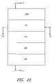
- FIG. 1Ais a schematic plan view of a memory array at a first stage of processing.
- FIG. 1Bis a schematic cross-section of the array of FIG. 1A along line 1 B— 1 B of FIG. 1A .
- FIG. 1Cis a schematic cross-section of the array of FIG. 1A along line 1 C— 1 C of FIG. 1A .
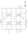
- FIG. 2Ais a schematic plan view of a memory array after formation of silicon pillars for the array.
- FIG. 2Bis a schematic cross-section of the array of FIG. 2A along line 2 B— 2 B of FIG. 2A .
- FIG. 2Cis a schematic cross-section of the array of FIG. 2A along line 2 C— 2 C of FIG. 2A .
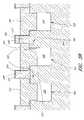
- FIG. 3Ais a schematic plan view of a memory array after formation of word lines for the array.
- FIG. 3Bis a schematic cross-section of the array of FIG. 3A along line 3 B— 3 B of FIG. 3A .
- FIG. 3Cis a schematic cross-section of the array of FIG. 3A along line 3 C— 3 C of FIG. 3A .
- FIG. 4Ais a schematic plan view of a memory array after planarization of vertical transistors of the array.
- FIG. 4Bis a schematic cross-section of the array of FIG. 4A along line 4 B— 4 B of FIG. 4A .
- FIG. 4Cis a schematic cross-section of the array of FIG. 4A along line 4 C— 4 C of FIG. 4A .
- FIG. 4Dis a schematic plan view of the memory array of FIG. 4A after formation of source regions.
- FIG. 5Ais a schematic plan view of a memory array after formation of digit lines for the array.
- FIG. 5Bis a schematic cross-section of the array of FIG. 5A along line 5 B— 5 B of FIG. 5A .
- FIG. 5Cis a schematic cross-section of the array of FIG. 5A along line 5 C— 5 C of FIG. 5A .
- FIG. 6Ais a schematic cross-section of the array of FIG. 5A after formation of cell capacitors to complete the memory cells.
- FIG. 6Bis a schematic three dimensional view of the array of FIG. 5A after formation of cell capacitors to complete the memory cells.
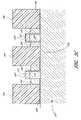
- FIG. 7is a schematic cross-section illustrating an alternative embodiment to FIG. 3B .
- semiconductor substrateis defined to mean any construction comprising semiconductor materials, including, but not limited to, bulk semiconductor materials such as a semiconductor wafer (either alone or in assemblies comprising other materials thereon), and semiconductor material layers (either alone or in assemblies comprising other materials).
- substraterefers to any supporting substrate, including, but not limited to, the semiconductor substrates described above.
- layerencompasses both the singular and the plural unless otherwise indicated.
- a vertical transistorIn small (e.g. 4F 2 ) memory cell designs, a vertical transistor can be used. These transistors typically use silicon pillars to form at least a portion of the active region. Silicon pillars can be formed using multiple masks and providing a spacer lining sidewalls of small windows before selectively growing epitaxial silicon within the windows.
- SEGselective epitaxial growth
- the size of the memory cellis 2F ⁇ 2F, or 4F 2 , meaning that each side of the memory cell measures only two times the minimum feature size (F) that can be provided for using the lithography processes for the process node.
- the Brown process used to form the epitaxial postsprovides a consistent and efficient method of forming epitaxial silicon posts to be used for vertical transistors.
- the floating body effectwhich can cause a cell capacitor to discharge and cause memory faults, commonly exists in memory cells that use vertical transistors.
- the floating body effectoccurs when an active region on the pillar, typically the drain, becomes isolated from the substrate.
- the sourcecould also be positioned at the top of the transistor pillar.
- the draincan be isolated by a dielectric layer or by the depletion region of a lower active area. When this occurs, the upper active area can charge up and cause the cell capacitor to discharge when it is supposed to remain in a charged state (i.e., when the transistor is ostensibly “off”). Ultimately, this will cause memory faults in the array.
- One method of reducing the floating body effectinvolves the use of a gate extending below an area that might cut off the active region on the top of the pillar from the substrate.
- An example of thisis extending the gate below a depletion region to tie the upper active area to the substrate.
- IEDMInternational Electron Devices Meeting
- That articleis hereby incorporated herein by reference.
- a word lineis formed surrounding the epitaxially grown silicon pillars and recessed into the field oxide such that the lowest point of the word line is beneath the highest point of the source region.
- the word linecreates a p-type region in the silicon pillar that it surrounds. This creates a channel in which charge can move from the drain down to the substrate.
- a p-well 190is formed within a semiconductor substrate 204 before forming masks 208 , 209 ( FIG. 1A ) on the substrate.
- the formation of the masks 208 , 209is discussed below.
- the p-well 190extends from the surface of the substrate to a depth of between about 5,000 ⁇ and 10,000 ⁇ , more preferably between about 8,000 ⁇ and 9,000 ⁇ . Skilled practitioners will appreciate that there are several ways to form the p-well region.
- isolation trenches 202( FIG. 1B ) and substrate ridges 203 ( FIG. 1B ) are defined within the substrate.
- the isolation trenches 202 and the upper substrate ridges 203preferably run vertically in FIG. 1A , (i.e. parallel to line 1 C— 1 C).
- the trenchescan be formed by forming a mask over the semiconductor substrate 204 and etching the substrate 204 .
- the substrate in the arrayis etched to a depth of between about 2000 ⁇ and 4000 ⁇ , more preferably between about 2500 ⁇ and 3500 ⁇ . As seen in FIG.
- the isolation trench 202is filled with a field isolation material, such as field oxide 205 .
- the field oxide 205is formed primarily using a spin-on deposition (SOD) oxide.
- the field oxide 205may have additional layers.
- the field oxide 205may comprise, starting from the trench walls, a thin thermal oxide layer (e.g., less than about 100 ⁇ ), a thin nitride layer (e.g., less than about 100 ⁇ ), a TEOS oxide layer (e.g., less than about 200 ⁇ ), and a thick spin-on oxide to fill the remainder of the trench (e.g., about 5,000 ⁇ ).
- FIG. 1Cillustrates the first mask 208 and the second mask 209 over the p-well 190 .
- the first mask 208is silicon nitride
- the second mask 209is silicon oxide.
- a pad oxideis formed on the surface of the substrate before the first mask 208 is formed.
- a liner 207is formed over the substrate and the first mask.
- the liner 207comprises the same material as the first mask.
- the first maskpreferably has a thickness of between about 2000 ⁇ and 3000 ⁇ .
- the regions that will form part of the transistor active areasare beneath the first mask 208 .
- the active areascan be doped prior to formation of the masks, or during subsequent processing.
- FIG. 1Ais a plan view of an array before formation of the epitaxial posts.
- Two mask patternsare shown over a substrate 204 .
- the first mask 208preferably nitride, is deposited and patterned to form lines over the substrate.
- the liner 207is formed in the gaps between lines of the first mask before the second mask 209 is formed between the lines of the first mask 208 .
- the second mask 209is an oxide such as a tetraethyl orthosilicate (TEOS) oxide or a spin-on deposition (SOD) oxide.
- TEOStetraethyl orthosilicate
- SODspin-on deposition
- the second mask 209has been patterned.
- the second maskis patterned by forming a perpendicular set of mask lines (not shown) and selectively etching to leave alternating blocks of mask and windows of exposed substrate.
- FIG. 2Bis a schematic cross-section along line 2 B— 2 B, and illustrates a spacer 210 lining the sidewalls of the window region above the exposed substrate.
- the spacer 210is an oxide such as a TEOS oxide.
- a blanket layer of oxideis deposited over the substrate 204 and into the windows.
- a spacer etchis then performed to etch the horizontal surfaces of the oxide, forming the spacer 210 and exposing a smaller window of the substrate 204 .
- a thin nitride layer(not shown) can be formed over the spacer 210 .
- the nitride layeris then spacer etched to allow for a hydrofluoric acid wet pre-clean step prior toe epitaxial deposition.
- Epitaxial silicon 220is then selectively grown in the narrowed window on the substrate ridge 203 .
- the epitaxial post 220has a shape that is approximately rectangular or square. However, the shape of the epitaxial post 220 can also be a cylinder, or other geometric shapes.
- the patterning of the second mask 209forms islands upon the substrate 204 .
- the islands of mask 209 and the lines of the first mask 208define the windows on the portions of the ridges 203 over which the narrower epitaxial posts 220 are formed.
- the silicon pillars 220are formed using selective epitaxial growth (SEG) techniques known in the art.
- the silicon pillars 220are formed as undoped epitaxial silicon.
- a p-type dopant, such as boron,is preferably implanted in the pillars after the epitaxial growth.
- the pillars 220are recessed to a preferred height above the substrate 204 .
- the silicon pillars 220have a height of between about 1200 ⁇ and 2000 ⁇ , more preferably between about 1400 ⁇ and 1800 ⁇ . Skilled practitioners will appreciate that the SEG step can use a variety of parameters to form the silicon pillars 220 .
- the drain region 221which is preferably situated on the top of the pillar 220 , can be formed by implanting an n-dopant in the top of the pillar.
- the upper active region 221 on the silicon pillar 220preferably serves as the drain of the transistor.
- the drain regions 221can be formed by implanting an n-dopant into the silicon pillars 220 , either immediately after the SEG step, or at a later stage of processing.
- the drain regions 221could also be formed by in situ doping during latter stages of SEG deposition after forming the channel or body of the pillar 220 as lightly p-doped silicon. Skilled practitioners will appreciate that the drain region can be doped at any of several different stages and by any of various different methods.
- FIGS. 3A–3Cthe second mask 209 and the spacers 210 have been removed.
- the silicon pillars 220can be seen in columns atop the ridges 203 in the substrate 204 .
- the field oxide 205is recessed within the isolation trench either during or after the process of removing the second mask 209 and spacers 210 .
- a buffered oxide etch (BOE) solutionwill be used to etch the oxide second mask 209 and spacers 210 .
- the nitride liner 207( FIG. 2B ) acts as an etch stop for the BOE etch process. A short wet nitride strip is then performed to remove the nitride liner 207 .
- an oxide dry etchpreferably selective to the first mask 208 and the epitaxial silicon 220 , is used to recess the field oxide 205 to a selected level.
- the selection of how far to recess the field oxideis based on both the floating body effect and gate capacitance.
- the gate 240can extend beneath the height of the silicon ridge 203 . While the timing of the recessing of the field oxide is described as being after the formation of the pillars 220 , the field oxide 205 can also be recessed at other processing stages. For example, the field oxide 205 can be recessed after the deposition of the first mask 208 and before the formation of the nitride layer 207 .
- a conformal dielectric layeris formed over exposed silicon, including the exposed portion of the substrate ridges 203 and the silicon pillars 220 .
- This dielectric layerwill serve as the gate dielectric 230 ( FIGS. 3B and 3C ) over the pillars 220 .
- a thermally grown gate oxide 230 formed over the substrate ridge 203will isolate the pillars 220 from the word lines 240 .
- the gate oxide 230is preferably formed by thermal oxidation or an oxide, such as a high dielectric constant oxide, could be deposited.
- the gate dielectric 230is formed to be quite thin.
- the gate dielectric 230is between about 10 ⁇ and 100 ⁇ , more preferably between about 60 ⁇ and 80 ⁇ .
- the word lines 240are deposited surrounding the gate dielectric 230 and over the field oxide 205 .
- Preferred materials for the word lineinclude doped poly or a fully silicided conductor, such as CoSi 2 or NiSi.
- a blanket layer of word line materialis deposited over the array.
- the word line materialis recessed back to form the word lines 240 , which act as gates for the vertical transistors.
- each word line 240will surround a row of pillars 220 running in a direction perpendicular to the trenches 202 and ridges 203 .
- drain regions 221 to the substrate 204are kept intact by the presence of the word line material 240 .
- Drain regions 221 , situated at the top of the pillars 220are thus “tied” to the substrate due to the lower extension of the gates 240 .
- the depth to which the field oxide 205 is recessed and the word lines 240 extend into the trenches 202is a balance between competing interests: the reduction of the floating body effect and the gate capacitance.
- the field oxideis recessed (and the word line 240 or gate extends downwardly) relative to the upper surface of the substrate ridge 203 by between about 0 ⁇ and 1500 ⁇ , more preferably between about 500 ⁇ and 1000 ⁇ .
- the depth to which the field oxide 205 is recessedcan be varied.
- the depletion regions that can cut off the pathway from the upper active region 221 to the substrate 204can be measured in several ways.
- a common way to measure the depletion regionis by measuring the midgap potential, the electrostatic potential in the substrate 204 at the center 243 of the ridge 203 between source regions. Because of the shape and location of the source regions 206 (namely on either side of but not beneath the pillars 220 ), they can be seen in FIG. 3C , but not FIG. 3B .
- the ridge 203 beneath and extending away from each pillar 220forms a part of the transistor channel.
- the electrostatic potentialis reduced directly beneath the drain 221 . Without using the recessed gate, depletion regions in the substrate can meet.
- the midgap potentialwas simulated to be approximately 1.5 eV. However by using the recessed gate, the midgap potential falls in simulations to approximately 0.1 eV.
- the use of the recessed word line 240causes a reduction in midgap potential of greater than about 75%, more preferably greater than 85%.
- FIGS. 4A–4Cshow vertical transistors after the deposition of an insulation layer 256 and a planarization of the upper surface down to the top of the first mask 208 . Because the first mask 208 is approximately 1000 ⁇ taller than the pillar, some of the insulation layer 256 will remain over the pillars 220 .
- the insulation layer 256is an oxide, such as undoped silicon glass (USG), borosilicate glass (BSG), phosphosilicate glass (PSG), or borophosphosilicate glass (BPSG).
- the upper surfaceis then planarized, preferably using a stop on nitride chemical mechanical polish (CMP) step. By using a stop-on-nitride CMP step, a sufficient insulation layer 256 will remain after the CMP step.
- CMPchemical mechanical polish
- the source regionsmay be formed after the planarization of the insulation layer 256 and before the formation of the digit lines.
- a mask 257is formed over the array of FIG. 4A .
- the mask 257is parallel to the substrate ridges 203 .
- the mask 257preferably covers half of the substrate ridge 203 and is over half of the field oxide 205 .
- the mask 257is used to remove a portion of the first mask 208 .
- a portion of the substrate ridge 203 and the field oxide 205will be exposed.
- the exposed region of the substrate ridge 203can be implanted with a dopant in order to form the source region 206 .
- an n-type dopantis implanted.
- the implantationpreferably does not substantially affect the properties of the exposed portion of the field oxide 205 .
- FIGS. 5A–5Cillustrate the formation of digit lines that will be buried by an interlayer dielectric, in which the cell capacitor is formed.
- FIG. 5Ba schematic cross-section is seen through a row of pillars 220 .
- the active areas of the transistori.e. the source and the drain
- the drain regions 221may be formed at several stages of processing when the top of the pillar 220 is exposed.
- the source regions 206are seen in FIG. 5C .
- the digit line 315which is over a digit line contact 310 , is seen over the field oxide 205 .
- the digit line 315runs perpendicular to and above the word line 240 .
- FIG. 5Cillustrates the formation of a digit line plug 305 to connect the digit line 315 to the source region 206 of the transistor.
- the digit line plug 305is offset from the isolation trench 202 by F/2 (i.e. half of the minimum printable feature size).
- the digit line plug 305is a conductive material, more preferably a polysilicon layer, most preferably n-doped poly.
- the digit line plug 305contacts the lower portion of the digit line 310 .
- the digit lineis multi-layered.
- the lower portion of the digit line 310 and the upper portion of the digit line 315are offset by F/2 as well. This allows the digit line 315 to be formed over the isolation trench 205 . Forming the digit line over the trench 205 can prevent interference caused by the digit line 310 and 315 .
- the lower portion of the digit line 310is metallic, such as a conductive nitride like titanium nitride. More preferably the lower portion of the digit line 310 is metal mode titanium nitride, a TiN layer that has a high titanium concentration and is particularly conductive. Skilled artisans will appreciate that there are several methods of forming such a layer, including chemical vapor deposition (CVD) and atomic layer deposition (ALD).
- the upper portion of the digit line 315is a conductor, more preferably a highly conductive metal, most preferably tungsten.
- An insulating liner 320is preferably deposited around the digit line 310 and 315 .
- the insulating liner 320can also be deposited in a recess in the digit line plug 305 .
- An insulation layer 323is deposited over the upper portion of the digit line 315 .
- the insulation layer 323is a silicon nitride layer.
- the digit line layers 310 and 315 , and the insulation layer 323are formed by depositing blanket layers over the partially fabricated array of FIGS. 4A–4C .
- a photoresist maskis preferably formed in order to pattern these layers and an anisotropic etch process is used to etch them.
- the nitride liner 320can then be deposited over the edges of the digit line layers 310 and 315 , and the insulation layer 323 .
- a nitride punch or spacer etchis preferably formed to contact the silicon posts 220 . If the drain regions 221 have not been doped, they can be doped after the spacer etch is performed to expose the silicon posts 220 .
- An oxide layer 325is preferably deposited over the array before a planarization process, preferably a CMP step.
- a cell capacitoris formed over the vertical transistor to complete the memory cell.
- a container capacitoris formed over the vertical transistor.
- the oxide layer 325is removed over the silicon posts 320 and a cell contact plug 350 is formed.
- the plug 350is a conductor, more preferably the plug 350 is a polysilicon layer.
- a structural layer 360is formed over the insulating layer and the plug 350 .
- the structural layer 360is an oxide, such as BSG, PSG, or BPSG. The structural layer is masked and etched to form a recess over and exposing each plug 350 in the array.
- a lower capacitor electrode 365is conformally formed within the recess and over the structural layer.
- the lower electrodes 365are preferably etched or polished back to isolate each electrode from its neighboring cells.
- Preferred materials for the lower electrodes 365include metals, such as tungsten, metal compounds, such as titanium nitride, and polysilicon.
- a blanket layer of a capacitor dielectric 370is then conformally formed over the array.
- the capacitor dielectric 370does not need to be etched to be isolated from neighboring cells. Rather, in a preferred embodiment, the capacitor dielectric 370 can be one layer for the entire array.
- Preferred materials for the capacitor dielectric 370include metal oxides, such as tantalum oxide, aluminum oxide, hafnium oxide, and zirconium oxide.
- an upper electrode 375is formed over the array.
- the material for the upper electrode 375is preferably blanket deposited over the array.
- the upper electrodedoes not need to be isolated from neighboring cells; a single electrode layer 375 can serve as the upper or reference electrode for multiple capacitors or the whole array.
- Preferred materialsinclude metals, such as tungsten, and metal compounds, such as titanium nitride and tungsten silicide (WSi x ).
- the upper electrode 375can also comprise multiple films.
- the upper electrode 375can comprise a layer of titanium nitride, a layer of polysilicon, and a layer of tungsten silicide.
- FIG. 6Bshows a schematic three dimensional view of a cell. The word line 240 can be seen descending below the ridge 203 into the trench 202 .
- the structural layer 360can be removed prior to depositing the capacitor dielectric 370 . This would allow both the inside and the outside of the lower container electrode 365 to be used to increase the capacitance.
- the capacitor dielectric 370 and the upper electrode 375would then be formed conformally over the lower electrode 365 and over the insulating layer 323 .
- An insulatoris deposited over the array before the array is planarized, preferably using a CMP step.
- FIG. 7Another embodiment is illustrated in FIG. 7 , where the array is seen at the stage of processing corresponding to FIG. 3B of the first embodiment.
- a portion 242 of the substrate ridge 203 beneath the pillar 220is implanted with an n-type dopant before the word lines 240 are formed. This extends the source regions 206 to overlap with the pillars 220 .
- This extended source 242can be formed directly beneath the pillar 220 , or it can stop at the edge of the pillar 220 . This allows the depletion field to spread further down the silicon post 220 rather than through the whole width of the silicon post.
- the doped portion 242is preferably formed before the word line is formed and after the active areas and the isolation trenches are formed. In a preferred embodiment, the doped portion 242 is used in combination with the word line 240 dropped into the field oxide 205 .
- N-doped source regions 206are formed in the array and can be seen FIG. 5B and serve as the source for the transistors.
- Isolation trenches 202are formed within a substrate 204 .
- a silicon pillar 220extends over a plateau or ridge 203 in the substrate 204 , so that it is bordered on two sides by a ledge 262 because the pillar 220 is narrower than the width of the substrate ridge 203 .
- the other two sides of the pillar 220are facing the length of the substrate ridge 203 .
- the source region 206is formed in the substrate ridge 203 .
- the silicon pillar 220 and portions of the ridge 203are lined by a gate dielectric 230 .
- a word line 240which is dropped into the isolation trench 202 surrounds a row of silicon pillars 220 .
- the word line 240follows the gate dielectric 230 around the pillar and down along the sides of ledge 262 into the isolation trench 202 .
- An isolation material 256separates the word line 240 from the digit line conductors 310 and 315 , which is connected to the active area 206 through a digit line plug (not pictured).
- the pillars 220can also vary from the embodiments described herein.
- the pillar 220can be etched from the substrate, the pillar could take other shapes, or the doping could be opposite (i.e. n-doped versus p-doped) from those discussed above.
- the source region 206may be extended to overlap with the pillar 220 by doping an additional portion of the ridge 203 .
- a capacitor contact plugis connected to the silicon post 220 and to the lower capacitor electrode 365
- the lower electrodeis formed within a structural layer 360 .
- a capacitor dielectric 370is formed over the structural layer 360 and within the lower electrode 365 .
- An upper electrode layer 375is formed over the capacitor dielectric 370 .
- An insulatorcan be deposited over the array to isolate the array during subsequent processing.
- FIG. 6Bis a schematic three dimensional view of the cell, which omits several parts of the cell in order to clearly show the remaining parts.
- a drain 221is situated on the top of the pillar 220
- a source 206is situated within the silicon ridge slightly offset from the pillar 220 .
- a capacitor plug350 in FIG. 6A
- itis not shown over the drain in FIG. 6B in order to show the relative position of the capacitor 330 to the digit line layers 310 and 315 .
- the layer 310is shown only with the plug 305 underneath it.
- the digit line layers 310 and 315are also supported over the substrate 204 by the oxide layer 256 ( FIG.
- the sourcecontacts the digit line plug 305 in order to form an electrical connection with the digit line.
- An insulator layer 323is over the digit line.
- the capacitor 330positioned over the drain 221 , is shown only schematically in FIG. 6B , but is preferably a container capacitor as described in reference to FIG. 6A .
Landscapes
- Engineering & Computer Science (AREA)
- Manufacturing & Machinery (AREA)
- Semiconductor Memories (AREA)
Abstract
Description
Claims (24)
Priority Applications (4)
| Application Number | Priority Date | Filing Date | Title |
|---|---|---|---|
| US11/010,752US7199419B2 (en) | 2004-12-13 | 2004-12-13 | Memory structure for reduced floating body effect |
| US11/437,999US7183164B2 (en) | 2004-12-13 | 2006-05-18 | Methods of reducing floating body effect |
| US11/673,968US7368344B2 (en) | 2004-12-13 | 2007-02-12 | Methods of reducing floating body effect |
| US11/673,922US7626223B2 (en) | 2004-12-13 | 2007-02-12 | Memory structure for reduced floating body effect |
Applications Claiming Priority (1)
| Application Number | Priority Date | Filing Date | Title |
|---|---|---|---|
| US11/010,752US7199419B2 (en) | 2004-12-13 | 2004-12-13 | Memory structure for reduced floating body effect |
Related Child Applications (2)
| Application Number | Title | Priority Date | Filing Date |
|---|---|---|---|
| US11/437,999DivisionUS7183164B2 (en) | 2004-12-13 | 2006-05-18 | Methods of reducing floating body effect |
| US11/673,922ContinuationUS7626223B2 (en) | 2004-12-13 | 2007-02-12 | Memory structure for reduced floating body effect |
Publications (2)
| Publication Number | Publication Date |
|---|---|
| US20060125044A1 US20060125044A1 (en) | 2006-06-15 |
| US7199419B2true US7199419B2 (en) | 2007-04-03 |
Family
ID=36582831
Family Applications (4)
| Application Number | Title | Priority Date | Filing Date |
|---|---|---|---|
| US11/010,752Expired - LifetimeUS7199419B2 (en) | 2004-12-13 | 2004-12-13 | Memory structure for reduced floating body effect |
| US11/437,999Expired - LifetimeUS7183164B2 (en) | 2004-12-13 | 2006-05-18 | Methods of reducing floating body effect |
| US11/673,968Expired - LifetimeUS7368344B2 (en) | 2004-12-13 | 2007-02-12 | Methods of reducing floating body effect |
| US11/673,922Expired - LifetimeUS7626223B2 (en) | 2004-12-13 | 2007-02-12 | Memory structure for reduced floating body effect |
Family Applications After (3)
| Application Number | Title | Priority Date | Filing Date |
|---|---|---|---|
| US11/437,999Expired - LifetimeUS7183164B2 (en) | 2004-12-13 | 2006-05-18 | Methods of reducing floating body effect |
| US11/673,968Expired - LifetimeUS7368344B2 (en) | 2004-12-13 | 2007-02-12 | Methods of reducing floating body effect |
| US11/673,922Expired - LifetimeUS7626223B2 (en) | 2004-12-13 | 2007-02-12 | Memory structure for reduced floating body effect |
Country Status (1)
| Country | Link |
|---|---|
| US (4) | US7199419B2 (en) |
Cited By (42)
| Publication number | Priority date | Publication date | Assignee | Title |
|---|---|---|---|---|
| US20060046440A1 (en)* | 2004-09-01 | 2006-03-02 | Nirmal Ramaswamy | Methods of forming layers comprising epitaxial silicon |
| US20060258084A1 (en)* | 2004-09-02 | 2006-11-16 | Tang Sanh D | Vertical transistors |
| US20070020851A1 (en)* | 2005-07-25 | 2007-01-25 | Freescale Semiconductor, Inc. | Hot carrier injection programmable structure including discontinuous storage elements and spacer control gates in a trench and a method of using the same |
| US20070018232A1 (en)* | 2005-07-25 | 2007-01-25 | Freescale Semiconductor, Inc. | Nonvolatile storage array with continuous control gate employing hot carrier injection programming |
| US20070020831A1 (en)* | 2005-07-25 | 2007-01-25 | Freescale Semiconductor, Inc. | Method of fabricating a nonvolatile storage array with continuous control gate employing hot carrier injection programming |
| US20070018221A1 (en)* | 2005-07-25 | 2007-01-25 | Freescale Semiconductor, Inc. | Programmable structure including discontinuous storage elements and spacer control gates in a trench |
| US20070019472A1 (en)* | 2005-07-25 | 2007-01-25 | Freescale Semiconductor, Inc. | Electronic device including a memory array and conductive lines |
| US20070020845A1 (en)* | 2005-07-25 | 2007-01-25 | Freescale Semiconductor, Inc. | Method of fabricating programmable structure including discontinuous storage elements and spacer control gates in a trench |
| US20070020840A1 (en)* | 2005-07-25 | 2007-01-25 | Freescale Semiconductor, Inc. | Programmable structure including nanocrystal storage elements in a trench |
| US20070018229A1 (en)* | 2005-07-25 | 2007-01-25 | Freescale Semiconductor, Inc. | Electronic device including discontinuous storage elements and a process for forming the same |
| US20070066019A1 (en)* | 2005-07-06 | 2007-03-22 | Leonard Forbes | Surround gate access transistors with grown ultra-thin bodies |
| US20070228437A1 (en)* | 2005-02-03 | 2007-10-04 | Micron Technology, Inc. | DRAM Arrays, Vertical Transistor Structures, and Methods of Forming Transistor Structures and DRAM Arrays |
| US7371627B1 (en) | 2005-05-13 | 2008-05-13 | Micron Technology, Inc. | Memory array with ultra-thin etched pillar surround gate access transistors and buried data/bit lines |
| US7399675B2 (en) | 2004-10-08 | 2008-07-15 | Freescale Semiconductor, Inc | Electronic device including an array and process for forming the same |
| US7510954B1 (en) | 2005-05-13 | 2009-03-31 | Micron Technology, Inc. | Memory array with surrounding gate access transistors and capacitors with global and staggered local bit lines |
| US20090170261A1 (en)* | 2007-12-28 | 2009-07-02 | Hynix Semiconductor Inc. | Method for manufacturing semiconductor device having 4f2 transistor |
| US20090179231A1 (en)* | 2004-09-01 | 2009-07-16 | Nirmal Ramaswamy | Integrated Circuitry |
| US7566620B2 (en) | 2005-07-25 | 2009-07-28 | Micron Technology, Inc. | DRAM including a vertical surround gate transistor |
| US7572699B2 (en) | 2007-01-24 | 2009-08-11 | Freescale Semiconductor, Inc | Process of forming an electronic device including fins and discontinuous storage elements |
| US7582929B2 (en) | 2005-07-25 | 2009-09-01 | Freescale Semiconductor, Inc | Electronic device including discontinuous storage elements |
| US7592224B2 (en) | 2006-03-30 | 2009-09-22 | Freescale Semiconductor, Inc | Method of fabricating a storage device including decontinuous storage elements within and between trenches |
| US7619275B2 (en) | 2005-07-25 | 2009-11-17 | Freescale Semiconductor, Inc. | Process for forming an electronic device including discontinuous storage elements |
| US7619270B2 (en) | 2005-07-25 | 2009-11-17 | Freescale Semiconductor, Inc. | Electronic device including discontinuous storage elements |
| US7642594B2 (en) | 2005-07-25 | 2010-01-05 | Freescale Semiconductor, Inc | Electronic device including gate lines, bit lines, or a combination thereof |
| US7651916B2 (en) | 2007-01-24 | 2010-01-26 | Freescale Semiconductor, Inc | Electronic device including trenches and discontinuous storage elements and processes of forming and using the same |
| US20100041191A1 (en)* | 2008-08-15 | 2010-02-18 | Anderson Brent A | Split-gate dram with mugfet, design structure, and method of manufacture |
| US20100038694A1 (en)* | 2008-08-15 | 2010-02-18 | Anderson Brent A | Split-gate dram with mugfet, design structure, and method of manufacture |
| US7696567B2 (en) | 2005-08-31 | 2010-04-13 | Micron Technology, Inc | Semiconductor memory device |
| US20100102361A1 (en)* | 2008-10-29 | 2010-04-29 | Nanya Technology Corporation | Vertical transistor and fabricating method thereof and vertical transistor array |
| US20100252886A1 (en)* | 2006-08-22 | 2010-10-07 | Micron Technology, Inc. | Fin structures and methods of fabricating fin structures |
| US20100289085A1 (en)* | 2009-05-14 | 2010-11-18 | International Business Machines Corporation | Asymmetric Semiconductor Devices and Method of Fabricating |
| US7838922B2 (en) | 2007-01-24 | 2010-11-23 | Freescale Semiconductor, Inc. | Electronic device including trenches and discontinuous storage elements |
| US7858471B2 (en) | 2006-09-13 | 2010-12-28 | Micron Technology, Inc. | Methods of fabricating an access transistor for an integrated circuit device, methods of fabricating periphery transistors and access transistors, and methods of fabricating an access device comprising access transistors in an access circuitry region and peripheral transistors in a peripheral circuitry region spaced from the access circuitry region |
| US20110062518A1 (en)* | 2009-09-17 | 2011-03-17 | International Business Machines Corporation | finFETS AND METHODS OF MAKING SAME |
| US20110169064A1 (en)* | 2010-01-11 | 2011-07-14 | International Business Machines Corporation | Read transistor for single poly non-volatile memory using body contacted soi device |
| US20120100707A1 (en)* | 2010-10-26 | 2012-04-26 | Ryu Choon-Kun | Method for fabricating non-volatile memory device with three-dimensional structure |
| US8184472B2 (en) | 2009-03-13 | 2012-05-22 | International Business Machines Corporation | Split-gate DRAM with lateral control-gate MuGFET |
| US8274106B2 (en) | 2004-07-20 | 2012-09-25 | Micron Technology, Inc. | DRAM layout with vertical FETs and method of formation |
| US9287271B2 (en) | 2011-08-23 | 2016-03-15 | Micron Technology, Inc. | Vertical transistor devices, memory arrays, and methods of forming vertical transistor devices |
| US9564442B2 (en) | 2015-04-08 | 2017-02-07 | Micron Technology, Inc. | Methods of forming contacts for a semiconductor device structure, and related methods of forming a semiconductor device structure |
| US10515801B2 (en) | 2007-06-04 | 2019-12-24 | Micron Technology, Inc. | Pitch multiplication using self-assembling materials |
| US11257766B1 (en) | 2020-08-21 | 2022-02-22 | Micron Technology, Inc. | Methods of forming microelectronic devices, and related microelectronic devices, memory devices, and electronic systems |
Families Citing this family (26)
| Publication number | Priority date | Publication date | Assignee | Title |
|---|---|---|---|---|
| US7531395B2 (en)* | 2004-09-01 | 2009-05-12 | Micron Technology, Inc. | Methods of forming a layer comprising epitaxial silicon, and methods of forming field effect transistors |
| US7144779B2 (en)* | 2004-09-01 | 2006-12-05 | Micron Technology, Inc. | Method of forming epitaxial silicon-comprising material |
| JP2008066562A (en)* | 2006-09-08 | 2008-03-21 | Toshiba Corp | Semiconductor device and manufacturing method thereof |
| JP2008108785A (en)* | 2006-10-23 | 2008-05-08 | Nec Electronics Corp | Semiconductor device and manufacturing method thereof |
| US8058683B2 (en)* | 2007-01-18 | 2011-11-15 | Samsung Electronics Co., Ltd. | Access device having vertical channel and related semiconductor device and a method of fabricating the access device |
| US7719869B2 (en)* | 2007-11-19 | 2010-05-18 | Qimonda Ag | Memory cell array comprising floating body memory cells |
| US7824983B2 (en)* | 2008-06-02 | 2010-11-02 | Micron Technology, Inc. | Methods of providing electrical isolation in semiconductor structures |
| DE102008030853B4 (en)* | 2008-06-30 | 2014-04-30 | Globalfoundries Dresden Module One Limited Liability Company & Co. Kg | Three-dimensional transistor with a dual-channel configuration |
| US8227867B2 (en)* | 2008-12-23 | 2012-07-24 | International Business Machines Corporation | Body contacted hybrid surface semiconductor-on-insulator devices |
| US8207032B2 (en)* | 2010-08-31 | 2012-06-26 | Micron Technology, Inc. | Methods of forming pluralities of vertical transistors, and methods of forming memory arrays |
| US9064745B2 (en) | 2012-08-29 | 2015-06-23 | International Business Machines Corporation | Sublithographic width finFET employing solid phase epitaxy |
| US9245987B2 (en) | 2012-11-29 | 2016-01-26 | Micron Technology, Inc. | Semiconductor devices and fabrication methods |
| US10128750B2 (en) | 2016-03-04 | 2018-11-13 | Infineon Technologies Ag | Switched-mode power converter with an inductive storage element and a cascode circuit |
| US9985126B2 (en)* | 2016-03-04 | 2018-05-29 | Infineon Technologies Ag | Semiconductor device comprising a first gate electrode and a second gate electrode |
| US9755073B1 (en)* | 2016-05-11 | 2017-09-05 | International Business Machines Corporation | Fabrication of vertical field effect transistor structure with strained channels |
| CN109155145B (en) | 2016-08-31 | 2022-11-01 | 美光科技公司 | Memory array |
| US10355002B2 (en) | 2016-08-31 | 2019-07-16 | Micron Technology, Inc. | Memory cells, methods of forming an array of two transistor-one capacitor memory cells, and methods used in fabricating integrated circuitry |
| EP3840046B1 (en) | 2016-08-31 | 2025-03-19 | Micron Technology, Inc. | Memory cells and memory arrays |
| WO2018044479A1 (en) | 2016-08-31 | 2018-03-08 | Micron Technology, Inc. | Sense amplifier constructions |
| CN109155311A (en) | 2016-08-31 | 2019-01-04 | 美光科技公司 | memory cell and memory array |
| US10056386B2 (en) | 2016-08-31 | 2018-08-21 | Micron Technology, Inc. | Memory cells and memory arrays |
| CN109155312B (en)* | 2016-08-31 | 2023-05-02 | 美光科技公司 | Memory cell and memory array |
| US11211384B2 (en) | 2017-01-12 | 2021-12-28 | Micron Technology, Inc. | Memory cells, arrays of two transistor-one capacitor memory cells, methods of forming an array of two transistor-one capacitor memory cells, and methods used in fabricating integrated circuitry |
| CN110753962A (en) | 2017-08-29 | 2020-02-04 | 美光科技公司 | memory circuit |
| CN108493188B (en)* | 2018-05-09 | 2023-10-13 | 长鑫存储技术有限公司 | Integrated circuit memory and formation method thereof, semiconductor integrated circuit device |
| US11171140B2 (en)* | 2020-03-18 | 2021-11-09 | Micron Technology, Inc. | Semiconductor memory device and method of forming the same |
Citations (7)
| Publication number | Priority date | Publication date | Assignee | Title |
|---|---|---|---|---|
| US4903344A (en) | 1987-07-07 | 1990-02-20 | Oki Electric Industry Co., Ltd. | Semiconductor memory device with staggered sense amplifiers |
| US6172391B1 (en)* | 1997-08-27 | 2001-01-09 | Siemens Aktiengesellschaft | DRAM cell arrangement and method for the manufacture thereof |
| US6320222B1 (en) | 1998-09-01 | 2001-11-20 | Micron Technology, Inc. | Structure and method for reducing threshold voltage variations due to dopant fluctuations |
| US20020030214A1 (en)* | 2000-09-11 | 2002-03-14 | Fumio Horiguchi | Semiconductor device and method for manufacturing the same |
| US20030001290A1 (en)* | 2001-06-29 | 2003-01-02 | Kabushiki Kaisha Toshiba | Semiconductor memory device and method for manufacturing the same |
| US6531727B2 (en) | 2001-02-09 | 2003-03-11 | Micron Technology, Inc. | Open bit line DRAM with ultra thin body transistors |
| US6964895B2 (en)* | 2002-03-11 | 2005-11-15 | Monolithic System Technology, Inc. | Method of fabricating vertical one-transistor floating-body DRAM cell in bulk CMOS process with electrically isolated charge storage region |
Family Cites Families (82)
| Publication number | Priority date | Publication date | Assignee | Title |
|---|---|---|---|---|
| US3941629A (en)* | 1974-04-11 | 1976-03-02 | General Motors Corporation | Diaphragm formation on silicon substrate |
| JPS53148389A (en) | 1977-05-31 | 1978-12-23 | Fujitsu Ltd | Manufacture for semiconductor device |
| US4139442A (en) | 1977-09-13 | 1979-02-13 | International Business Machines Corporation | Reactive ion etching method for producing deep dielectric isolation in silicon |
| US4333964A (en)* | 1980-09-15 | 1982-06-08 | General Electric Company | Method of making integrated circuits |
| US4508757A (en)* | 1982-12-20 | 1985-04-02 | International Business Machines Corporation | Method of manufacturing a minimum bird's beak recessed oxide isolation structure |
| US4472459A (en)* | 1983-10-24 | 1984-09-18 | Rca Corporation | Local oxidation of silicon substrate using LPCVD silicon nitride |
| JPS60167349A (en) | 1984-02-09 | 1985-08-30 | Nec Corp | Semiconductor integrated circuit device |
| US4551910A (en)* | 1984-11-27 | 1985-11-12 | Intel Corporation | MOS Isolation processing |
| US4615762A (en)* | 1985-04-30 | 1986-10-07 | Rca Corporation | Method for thinning silicon |
| US4630356A (en) | 1985-09-19 | 1986-12-23 | International Business Machines Corporation | Method of forming recessed oxide isolation with reduced steepness of the birds' neck |
| US4789560A (en)* | 1986-01-08 | 1988-12-06 | Advanced Micro Devices, Inc. | Diffusion stop method for forming silicon oxide during the fabrication of IC devices |
| US4746630A (en) | 1986-09-17 | 1988-05-24 | Hewlett-Packard Company | Method for producing recessed field oxide with improved sidewall characteristics |
| US5149669A (en)* | 1987-03-06 | 1992-09-22 | Seiko Instruments Inc. | Method of forming an isolation region in a semiconductor device |
| JPS6467945A (en)* | 1987-09-08 | 1989-03-14 | Mitsubishi Electric Corp | Wiring layer formed on buried dielectric and manufacture thereof |
| JPH01100948A (en) | 1987-10-14 | 1989-04-19 | Fujitsu Ltd | Manufacturing method of semiconductor device |
| US5252504A (en) | 1988-05-02 | 1993-10-12 | Micron Technology, Inc. | Reverse polysilicon CMOS fabrication |
| JPH02219253A (en) | 1989-02-20 | 1990-08-31 | Sumitomo Metal Ind Ltd | Manufacture of semiconductor integrated circuit device |
| US4959325A (en) | 1989-02-24 | 1990-09-25 | Micron Technology, Inc. | Reduction of electric field effect in the bird's beak region of a DRAM cell following expansion of active region through local encroachment reduction |
| US4965221A (en)* | 1989-03-15 | 1990-10-23 | Micron Technology, Inc. | Spacer isolation method for minimizing parasitic sidewall capacitance and creating fully recessed field oxide regions |
| JP2512216B2 (en)* | 1989-08-01 | 1996-07-03 | 松下電器産業株式会社 | Method for manufacturing semiconductor device |
| IT1236601B (en) | 1989-12-22 | 1993-03-18 | Sgs Thomson Microelectronics | INTEGRATED SEMICONDUCTOR DEVICE OF EPROM TYPE WITH METAL CONNECTIONS OF SOURCE AND PROCEDURE FOR ITS MANUFACTURE. |
| US5057449A (en)* | 1990-03-26 | 1991-10-15 | Micron Technology, Inc. | Process for creating two thicknesses of gate oxide within a dynamic random access memory |
| JPH04130630A (en) | 1990-09-20 | 1992-05-01 | Fuji Electric Co Ltd | Oxide film for integrated circuit devices and its formation method |
| FR2667440A1 (en) | 1990-09-28 | 1992-04-03 | Philips Nv | PROCESS FOR PRODUCING PATTERNS FOR ALIGNING MASKS. |
| JPH04162528A (en) | 1990-10-24 | 1992-06-08 | Hitachi Ltd | Manufacturing method of semiconductor device |
| US5087586A (en)* | 1991-07-03 | 1992-02-11 | Micron Technology, Inc. | Process for creating fully-recessed field isolation regions by oxidizing a selectively-grown epitaxial silicon layer |
| US5260229A (en)* | 1991-08-30 | 1993-11-09 | Sgs-Thomson Microelectronics, Inc. | Method of forming isolated regions of oxide |
| US5358894A (en) | 1992-02-06 | 1994-10-25 | Micron Technology, Inc. | Oxidation enhancement in narrow masked field regions of a semiconductor wafer |
| US5409563A (en) | 1993-02-26 | 1995-04-25 | Micron Technology, Inc. | Method for etching high aspect ratio features |
| JPH06268173A (en)* | 1993-03-15 | 1994-09-22 | Toshiba Corp | Semiconductor memory device |
| JP3390208B2 (en) | 1993-05-26 | 2003-03-24 | ローム株式会社 | Semiconductor device manufacturing method |
| US5458999A (en) | 1993-06-24 | 1995-10-17 | Szabo; Gabor | Interferometric phase shifting method for high resolution microlithography |
| KR970003731B1 (en)* | 1993-10-14 | 1997-03-21 | 엘지반도체 주식회사 | Device isolation film manufacturing method of semiconductor device |
| US5438016A (en)* | 1994-03-02 | 1995-08-01 | Micron Semiconductor, Inc. | Method of semiconductor device isolation employing polysilicon layer for field oxide formation |
| US5414287A (en)* | 1994-04-25 | 1995-05-09 | United Microelectronics Corporation | Process for high density split-gate memory cell for flash or EPROM |
| US5466632A (en)* | 1994-05-26 | 1995-11-14 | United Microelectronics Corp. | Field oxide with curvilinear boundaries and method of producing the same |
| US7118988B2 (en)* | 1994-08-15 | 2006-10-10 | Buerger Jr Walter Richard | Vertically wired integrated circuit and method of fabrication |
| US5497017A (en)* | 1995-01-26 | 1996-03-05 | Micron Technology, Inc. | Dynamic random access memory array having a cross-point layout, tungsten digit lines buried in the substrate, and vertical access transistors |
| US5607874A (en)* | 1996-02-02 | 1997-03-04 | Taiwan Semiconductor Manufacturing Company, Ltd. | Method for fabricating a DRAM cell with a T shaped storage capacitor |
| US6455916B1 (en)* | 1996-04-08 | 2002-09-24 | Micron Technology, Inc. | Integrated circuit devices containing isolated dielectric material |
| US5789306A (en)* | 1996-04-18 | 1998-08-04 | Micron Technology, Inc. | Dual-masked field isolation |
| US5899727A (en)* | 1996-05-02 | 1999-05-04 | Advanced Micro Devices, Inc. | Method of making a semiconductor isolation region bounded by a trench and covered with an oxide to improve planarization |
| US5747377A (en)* | 1996-09-06 | 1998-05-05 | Powerchip Semiconductor Corp. | Process for forming shallow trench isolation |
| US5929477A (en)* | 1997-01-22 | 1999-07-27 | International Business Machines Corporation | Self-aligned diffused source vertical transistors with stack capacitors in a 4F-square memory cell array |
| US5990509A (en)* | 1997-01-22 | 1999-11-23 | International Business Machines Corporation | 2F-square memory cell for gigabit memory applications |
| US5909618A (en)* | 1997-07-08 | 1999-06-01 | Micron Technology, Inc. | Method of making memory cell with vertical transistor and buried word and body lines |
| US6150687A (en)* | 1997-07-08 | 2000-11-21 | Micron Technology, Inc. | Memory cell having a vertical transistor with buried source/drain and dual gates |
| TW327700B (en) | 1997-07-15 | 1998-03-01 | Mos Electronics Taiwan Inc | The method for using rough oxide mask to form isolating field oxide |
| US6306727B1 (en) | 1997-08-18 | 2001-10-23 | Micron Technology, Inc. | Advanced isolation process for large memory arrays |
| US5834359A (en)* | 1997-08-29 | 1998-11-10 | Vanguard International Semiconductor Corporation | Method of forming an isolation region in a semiconductor substrate |
| JP3983858B2 (en) | 1997-09-18 | 2007-09-26 | 富士通株式会社 | Semiconductor memory device |
| US5907170A (en)* | 1997-10-06 | 1999-05-25 | Micron Technology, Inc. | Circuit and method for an open bit line memory cell with a vertical transistor and trench plate trench capacitor |
| US6528837B2 (en) | 1997-10-06 | 2003-03-04 | Micron Technology, Inc. | Circuit and method for an open bit line memory cell with a vertical transistor and trench plate trench capacitor |
| US6246083B1 (en)* | 1998-02-24 | 2001-06-12 | Micron Technology, Inc. | Vertical gain cell and array for a dynamic random access memory |
| US6097065A (en)* | 1998-03-30 | 2000-08-01 | Micron Technology, Inc. | Circuits and methods for dual-gated transistors |
| US6104068A (en)* | 1998-09-01 | 2000-08-15 | Micron Technology, Inc. | Structure and method for improved signal processing |
| US6049106A (en) | 1999-01-14 | 2000-04-11 | Micron Technology, Inc. | Large grain single crystal vertical thin film polysilicon MOSFETs |
| US6316806B1 (en)* | 1999-03-31 | 2001-11-13 | Fairfield Semiconductor Corporation | Trench transistor with a self-aligned source |
| KR100821456B1 (en)* | 2000-08-14 | 2008-04-11 | 샌디스크 쓰리디 엘엘씨 | Dense array and charge storage device and manufacturing method thereof |
| DE10041749A1 (en)* | 2000-08-27 | 2002-03-14 | Infineon Technologies Ag | Vertical non-volatile semiconductor memory cell and method for its production |
| US6537870B1 (en)* | 2000-09-29 | 2003-03-25 | Infineon Technologies Ag | Method of forming an integrated circuit comprising a self aligned trench |
| US6559491B2 (en)* | 2001-02-09 | 2003-05-06 | Micron Technology, Inc. | Folded bit line DRAM with ultra thin body transistors |
| US6377070B1 (en)* | 2001-02-09 | 2002-04-23 | Micron Technology, Inc. | In-service programmable logic arrays with ultra thin vertical body transistors |
| US6424001B1 (en)* | 2001-02-09 | 2002-07-23 | Micron Technology, Inc. | Flash memory with ultra thin vertical body transistors |
| US6496034B2 (en)* | 2001-02-09 | 2002-12-17 | Micron Technology, Inc. | Programmable logic arrays with ultra thin body transistors |
| US6448601B1 (en)* | 2001-02-09 | 2002-09-10 | Micron Technology, Inc. | Memory address and decode circuits with ultra thin body transistors |
| US6566682B2 (en)* | 2001-02-09 | 2003-05-20 | Micron Technology, Inc. | Programmable memory address and decode circuits with ultra thin vertical body transistors |
| US6649476B2 (en)* | 2001-02-15 | 2003-11-18 | Micron Technology, Inc. | Monotonic dynamic-static pseudo-NMOS logic circuit and method of forming a logic gate array |
| JP4216483B2 (en)* | 2001-02-15 | 2009-01-28 | 株式会社東芝 | Semiconductor memory device |
| JP2003031693A (en)* | 2001-07-19 | 2003-01-31 | Toshiba Corp | Semiconductor memory |
| US6670642B2 (en) | 2002-01-22 | 2003-12-30 | Renesas Technology Corporation. | Semiconductor memory device using vertical-channel transistors |
| JP2003297033A (en)* | 2002-03-29 | 2003-10-17 | Fuji Photo Film Co Ltd | Recording tape cartridge |
| US6900521B2 (en)* | 2002-06-10 | 2005-05-31 | Micron Technology, Inc. | Vertical transistors and output prediction logic circuits containing same |
| US6756625B2 (en)* | 2002-06-21 | 2004-06-29 | Micron Technology, Inc. | Memory cell and method for forming the same |
| US6734484B2 (en)* | 2002-08-26 | 2004-05-11 | Intellignet Sources Development Corp. | Vertical transistor DRAM structure and its manufacturing methods |
| US6734482B1 (en)* | 2002-11-15 | 2004-05-11 | Micron Technology, Inc. | Trench buried bit line memory devices |
| US6956256B2 (en)* | 2003-03-04 | 2005-10-18 | Micron Technology Inc. | Vertical gain cell |
| TWI222180B (en)* | 2003-04-29 | 2004-10-11 | Nanya Technology Corp | Method for forming vertical transistor and trench capacitor |
| US7041575B2 (en)* | 2003-04-29 | 2006-05-09 | Micron Technology, Inc. | Localized strained semiconductor on insulator |
| US7091566B2 (en)* | 2003-11-20 | 2006-08-15 | International Business Machines Corp. | Dual gate FinFet |
| JP3927179B2 (en) | 2004-01-06 | 2007-06-06 | 株式会社東芝 | Semiconductor memory device and manufacturing method thereof |
| US7285812B2 (en)* | 2004-09-02 | 2007-10-23 | Micron Technology, Inc. | Vertical transistors |
- 2004
- 2004-12-13USUS11/010,752patent/US7199419B2/ennot_activeExpired - Lifetime
- 2006
- 2006-05-18USUS11/437,999patent/US7183164B2/ennot_activeExpired - Lifetime
- 2007
- 2007-02-12USUS11/673,968patent/US7368344B2/ennot_activeExpired - Lifetime
- 2007-02-12USUS11/673,922patent/US7626223B2/ennot_activeExpired - Lifetime
Patent Citations (7)
| Publication number | Priority date | Publication date | Assignee | Title |
|---|---|---|---|---|
| US4903344A (en) | 1987-07-07 | 1990-02-20 | Oki Electric Industry Co., Ltd. | Semiconductor memory device with staggered sense amplifiers |
| US6172391B1 (en)* | 1997-08-27 | 2001-01-09 | Siemens Aktiengesellschaft | DRAM cell arrangement and method for the manufacture thereof |
| US6320222B1 (en) | 1998-09-01 | 2001-11-20 | Micron Technology, Inc. | Structure and method for reducing threshold voltage variations due to dopant fluctuations |
| US20020030214A1 (en)* | 2000-09-11 | 2002-03-14 | Fumio Horiguchi | Semiconductor device and method for manufacturing the same |
| US6531727B2 (en) | 2001-02-09 | 2003-03-11 | Micron Technology, Inc. | Open bit line DRAM with ultra thin body transistors |
| US20030001290A1 (en)* | 2001-06-29 | 2003-01-02 | Kabushiki Kaisha Toshiba | Semiconductor memory device and method for manufacturing the same |
| US6964895B2 (en)* | 2002-03-11 | 2005-11-15 | Monolithic System Technology, Inc. | Method of fabricating vertical one-transistor floating-body DRAM cell in bulk CMOS process with electrically isolated charge storage region |
Non-Patent Citations (15)
| Title |
|---|
| Cho et al., "A novel pillar DRAM cell for 4Gbit and beyond," IEEE, 1998, pp. 38-39. |
| Denton et al., "Fully depleted dual-gated thin-film SOI P-MOSFET's fabricated in SOI islands with an isolated buried polysilicon backgate," IEEE Electron Device Letters, Nov. 1996, pp. 509-511, vol. 17, No. 11. |
| Doyle et al., "High performance fully-depleted tri-gate CMOS transistors," IEEE Electron Device Letters, Apr. 2003, pp. 263-265, vol. 24, No. 4. |
| Endoh et al., "2.4F<SUP>2 </SUP>memory cell technology with stacked-surrounding gate transistor (S-SGT) DRAM," IEEE Transactions On Electron Devices, Aug. 2001, pp. 1599-1603, vol. 48, No. 8. |
| Endoh et al., "Novel ultrahigh-density flash memory with a stacked-surrounding gate transistor (S-SGT) structured cell," IEEE Transactions on Electron Devices, Apr. 2003, pp. 945-951, Vol. 50, No. 4. |
| Forbes, "DRAM array with surrounding gate access transistors and capacitors over global bit lines," surroundingdisc4.doc, Sep. 14, 2004. |
| Goebel et al., "Fully depleted surrounding gate transistor (SGT) for 70 nm DRAM and beyond," IEEE, 2002, 4 pages. |
| Huang et al., "Sub-50 nm P-channel finFET," IEEE Transactions on Electron Devices, May 2001, pp. 880-886, vol. 48, No. 5. |
| Kedzierski et al., "High-performance symmetric-gate and CMOS-compatible V<SUB>1 </SUB>asymmetric-gate FinFET devices," IEEE, 2001, 4 pages. |
| Miyano et al., Numerical analysis of a cylindrical thin-pillar transistor (CYNTHIA), IEEE Transactions on Electron Devices, Aug. 1992, pp. 1876-1881, vol. 39, No. 8. |
| Nitayama et al., "Multi-pillar surrounding gate transistor (M-SGT) for compact and high-speed circuits," IEEE Transacions on Electron Devices, Mar. 1991, pp. 579-583, vol. 18, No. 3. |
| Sunouchi et al., "A surrounding gate transistor (SGT) cell for 64/256 Mbit DRAMs," IEEE, 1989, pp. 2.1.1-2.1.4. |
| Takato et al., "High performance CMOS surrounding gate transistor (SGT) for ultra high density LSIs," IEEE, 1988, 4 pages. |
| Terauchi et al., "A surrounding gate transistor (SGT) gain cell for ultra high density DRAMS," pp. 21-22. |
| Wong et al., "Self-aligned (top and bottom) double-gate MOSFET with a 25 nm thick silicon channel," IBM T.J. Watson Research Center, 4 pages. |
Cited By (87)
| Publication number | Priority date | Publication date | Assignee | Title |
|---|---|---|---|---|
| US8274106B2 (en) | 2004-07-20 | 2012-09-25 | Micron Technology, Inc. | DRAM layout with vertical FETs and method of formation |
| US8482047B2 (en) | 2004-07-20 | 2013-07-09 | Micron Technology, Inc. | DRAM layout with vertical FETS and method of formation |
| US20100258857A1 (en)* | 2004-09-01 | 2010-10-14 | Nirmal Ramaswamy | Method of Forming a Layer Comprising Epitaxial Silicon, and a Field Effect Transistor |
| US7807535B2 (en) | 2004-09-01 | 2010-10-05 | Micron Technology, Inc. | Methods of forming layers comprising epitaxial silicon |
| US7768036B2 (en) | 2004-09-01 | 2010-08-03 | Micron Technology, Inc. | Integrated circuitry |
| US20060046440A1 (en)* | 2004-09-01 | 2006-03-02 | Nirmal Ramaswamy | Methods of forming layers comprising epitaxial silicon |
| US8673706B2 (en) | 2004-09-01 | 2014-03-18 | Micron Technology, Inc. | Methods of forming layers comprising epitaxial silicon |
| US20090179231A1 (en)* | 2004-09-01 | 2009-07-16 | Nirmal Ramaswamy | Integrated Circuitry |
| US20070166962A1 (en)* | 2004-09-01 | 2007-07-19 | Nirmal Ramaswamy | Methods of forming layers comprising epitaxial silicon |
| US20060258084A1 (en)* | 2004-09-02 | 2006-11-16 | Tang Sanh D | Vertical transistors |
| US7521322B2 (en) | 2004-09-02 | 2009-04-21 | Micron Technology, Inc. | Vertical transistors |
| US7399675B2 (en) | 2004-10-08 | 2008-07-15 | Freescale Semiconductor, Inc | Electronic device including an array and process for forming the same |
| US7569876B2 (en)* | 2005-02-03 | 2009-08-04 | Micron Technology, Inc. | DRAM arrays, vertical transistor structures, and methods of forming transistor structures and DRAM arrays |
| US7824982B2 (en)* | 2005-02-03 | 2010-11-02 | Micron Technology, Inc. | DRAM arrays, vertical transistor structures, and methods of forming transistor structures and DRAM arrays |
| US20070228437A1 (en)* | 2005-02-03 | 2007-10-04 | Micron Technology, Inc. | DRAM Arrays, Vertical Transistor Structures, and Methods of Forming Transistor Structures and DRAM Arrays |
| US20080093644A1 (en)* | 2005-02-03 | 2008-04-24 | Micron Technology, Inc. | DRAM Arrays, Vertical Transistor Structures, and Methods of Forming Transistor Structures and DRAM Arrays |
| US7525141B1 (en) | 2005-05-13 | 2009-04-28 | Micron Technology, Inc. | Memory array with ultra-thin etched pillar surround gate access transistors and buried data/bit lines |
| US8609523B2 (en) | 2005-05-13 | 2013-12-17 | Micron Technology, Inc. | Method of making a memory array with surrounding gate access transistors and capacitors with global staggered local bit lines |
| US7371627B1 (en) | 2005-05-13 | 2008-05-13 | Micron Technology, Inc. | Memory array with ultra-thin etched pillar surround gate access transistors and buried data/bit lines |
| US7910972B2 (en) | 2005-05-13 | 2011-03-22 | Micron Technology, Inc. | Memory array with ultra-thin etched pillar surround gate access transistors and buried data/bit lines |
| US8227305B2 (en) | 2005-05-13 | 2012-07-24 | Micron Technology, Inc. | Memory array with ultra-thin etched pillar surround gate access transistors and buried data/bit lines |
| US7510954B1 (en) | 2005-05-13 | 2009-03-31 | Micron Technology, Inc. | Memory array with surrounding gate access transistors and capacitors with global and staggered local bit lines |
| US8637362B2 (en) | 2005-05-13 | 2014-01-28 | Micron Technology, Inc. | Memory array with ultra-thin etched pillar surround gate access transistors and buried data/bit lines |
| US8350320B2 (en) | 2005-05-13 | 2013-01-08 | Micron Technology, Inc. | Memory array and memory device |
| US8101992B2 (en) | 2005-05-13 | 2012-01-24 | Micron Technology, Inc. | Memory array with surrounding gate access transistors and capacitors with global and staggered local bit lines |
| US7888721B2 (en) | 2005-07-06 | 2011-02-15 | Micron Technology, Inc. | Surround gate access transistors with grown ultra-thin bodies |
| US7626219B2 (en) | 2005-07-06 | 2009-12-01 | Micron Technology, Inc. | Surround gate access transistors with grown ultra-thin bodies |
| US20070066019A1 (en)* | 2005-07-06 | 2007-03-22 | Leonard Forbes | Surround gate access transistors with grown ultra-thin bodies |
| US7601595B2 (en) | 2005-07-06 | 2009-10-13 | Micron Technology, Inc. | Surround gate access transistors with grown ultra-thin bodies |
| US8115243B2 (en) | 2005-07-06 | 2012-02-14 | Micron Technology, Inc. | Surround gate access transistors with grown ultra-thin bodies |
| US7619270B2 (en) | 2005-07-25 | 2009-11-17 | Freescale Semiconductor, Inc. | Electronic device including discontinuous storage elements |
| US7768051B2 (en) | 2005-07-25 | 2010-08-03 | Micron Technology, Inc. | DRAM including a vertical surround gate transistor |
| US7285819B2 (en) | 2005-07-25 | 2007-10-23 | Freescale Semiconductor, Inc. | Nonvolatile storage array with continuous control gate employing hot carrier injection programming |
| US7314798B2 (en) | 2005-07-25 | 2008-01-01 | Freescale Semiconductor, Inc. | Method of fabricating a nonvolatile storage array with continuous control gate employing hot carrier injection programming |
| US7619275B2 (en) | 2005-07-25 | 2009-11-17 | Freescale Semiconductor, Inc. | Process for forming an electronic device including discontinuous storage elements |
| US20080019178A1 (en)* | 2005-07-25 | 2008-01-24 | Freescale Semiconductor, Inc. | Electronic device including a memory array and conductive lines |
| US7566620B2 (en) | 2005-07-25 | 2009-07-28 | Micron Technology, Inc. | DRAM including a vertical surround gate transistor |
| US7642594B2 (en) | 2005-07-25 | 2010-01-05 | Freescale Semiconductor, Inc | Electronic device including gate lines, bit lines, or a combination thereof |
| US20070020840A1 (en)* | 2005-07-25 | 2007-01-25 | Freescale Semiconductor, Inc. | Programmable structure including nanocrystal storage elements in a trench |
| US20070018229A1 (en)* | 2005-07-25 | 2007-01-25 | Freescale Semiconductor, Inc. | Electronic device including discontinuous storage elements and a process for forming the same |
| US7394686B2 (en) | 2005-07-25 | 2008-07-01 | Freescale Semiconductor, Inc. | Programmable structure including discontinuous storage elements and spacer control gates in a trench |
| US20070020845A1 (en)* | 2005-07-25 | 2007-01-25 | Freescale Semiconductor, Inc. | Method of fabricating programmable structure including discontinuous storage elements and spacer control gates in a trench |
| US7262997B2 (en)* | 2005-07-25 | 2007-08-28 | Freescale Semiconductor, Inc. | Process for operating an electronic device including a memory array and conductive lines |
| US20070019472A1 (en)* | 2005-07-25 | 2007-01-25 | Freescale Semiconductor, Inc. | Electronic device including a memory array and conductive lines |
| US7471560B2 (en) | 2005-07-25 | 2008-12-30 | Freescale Semiconductor, Inc. | Electronic device including a memory array and conductive lines |
| US7582929B2 (en) | 2005-07-25 | 2009-09-01 | Freescale Semiconductor, Inc | Electronic device including discontinuous storage elements |
| US20070018221A1 (en)* | 2005-07-25 | 2007-01-25 | Freescale Semiconductor, Inc. | Programmable structure including discontinuous storage elements and spacer control gates in a trench |
| US20070020831A1 (en)* | 2005-07-25 | 2007-01-25 | Freescale Semiconductor, Inc. | Method of fabricating a nonvolatile storage array with continuous control gate employing hot carrier injection programming |
| US20070018232A1 (en)* | 2005-07-25 | 2007-01-25 | Freescale Semiconductor, Inc. | Nonvolatile storage array with continuous control gate employing hot carrier injection programming |
| US7459744B2 (en) | 2005-07-25 | 2008-12-02 | Freescale Semiconductor, Inc. | Hot carrier injection programmable structure including discontinuous storage elements and spacer control gates in a trench and a method of using the same |
| US20070020851A1 (en)* | 2005-07-25 | 2007-01-25 | Freescale Semiconductor, Inc. | Hot carrier injection programmable structure including discontinuous storage elements and spacer control gates in a trench and a method of using the same |
| US7696567B2 (en) | 2005-08-31 | 2010-04-13 | Micron Technology, Inc | Semiconductor memory device |
| US7592224B2 (en) | 2006-03-30 | 2009-09-22 | Freescale Semiconductor, Inc | Method of fabricating a storage device including decontinuous storage elements within and between trenches |
| US20100252886A1 (en)* | 2006-08-22 | 2010-10-07 | Micron Technology, Inc. | Fin structures and methods of fabricating fin structures |
| US9281402B2 (en) | 2006-08-22 | 2016-03-08 | Micron Technology, Inc. | Methods of fabricating fin structures |
| US8748280B2 (en) | 2006-08-22 | 2014-06-10 | Micron Technology, Inc. | Methods of fabricating fin structures |
| US8076721B2 (en) | 2006-08-22 | 2011-12-13 | Micron Technology, Inc. | Fin structures and methods of fabricating fin structures |
| US7858471B2 (en) | 2006-09-13 | 2010-12-28 | Micron Technology, Inc. | Methods of fabricating an access transistor for an integrated circuit device, methods of fabricating periphery transistors and access transistors, and methods of fabricating an access device comprising access transistors in an access circuitry region and peripheral transistors in a peripheral circuitry region spaced from the access circuitry region |
| US7998813B2 (en) | 2006-09-13 | 2011-08-16 | Micron Technology, Inc. | Methods of fabricating an access transistor having a polysilicon-comprising plug on individual of opposing sides of gate material |
| US20100096686A1 (en)* | 2007-01-24 | 2010-04-22 | Freescale Semiconductor, Inc. | Electronic device including trenches and discontinuous storage elements |
| US8193572B2 (en) | 2007-01-24 | 2012-06-05 | Freescale Semiconductor, Inc. | Electronic device including trenches and discontinuous storage elements |
| US7572699B2 (en) | 2007-01-24 | 2009-08-11 | Freescale Semiconductor, Inc | Process of forming an electronic device including fins and discontinuous storage elements |
| US7651916B2 (en) | 2007-01-24 | 2010-01-26 | Freescale Semiconductor, Inc | Electronic device including trenches and discontinuous storage elements and processes of forming and using the same |
| US7838922B2 (en) | 2007-01-24 | 2010-11-23 | Freescale Semiconductor, Inc. | Electronic device including trenches and discontinuous storage elements |
| US10515801B2 (en) | 2007-06-04 | 2019-12-24 | Micron Technology, Inc. | Pitch multiplication using self-assembling materials |
| US20090170261A1 (en)* | 2007-12-28 | 2009-07-02 | Hynix Semiconductor Inc. | Method for manufacturing semiconductor device having 4f2 transistor |
| US7927945B2 (en) | 2007-12-28 | 2011-04-19 | Hynix Semiconductor Inc. | Method for manufacturing semiconductor device having 4F2 transistor |
| KR100950472B1 (en) | 2007-12-28 | 2010-03-31 | 주식회사 하이닉스반도체 | Manufacturing Method of Semiconductor Device Having 4F2 Transistor |
| US20100041191A1 (en)* | 2008-08-15 | 2010-02-18 | Anderson Brent A | Split-gate dram with mugfet, design structure, and method of manufacture |
| US20100038694A1 (en)* | 2008-08-15 | 2010-02-18 | Anderson Brent A | Split-gate dram with mugfet, design structure, and method of manufacture |
| US7781283B2 (en) | 2008-08-15 | 2010-08-24 | International Business Machines Corporation | Split-gate DRAM with MuGFET, design structure, and method of manufacture |
| US7979836B2 (en) | 2008-08-15 | 2011-07-12 | International Business Machines Corporation | Split-gate DRAM with MuGFET, design structure, and method of manufacture |
| US7928490B2 (en) | 2008-10-29 | 2011-04-19 | Nanya Technology Corporation | Vertical transistor and vertical transistor array |
| US20100102361A1 (en)* | 2008-10-29 | 2010-04-29 | Nanya Technology Corporation | Vertical transistor and fabricating method thereof and vertical transistor array |
| US8184472B2 (en) | 2009-03-13 | 2012-05-22 | International Business Machines Corporation | Split-gate DRAM with lateral control-gate MuGFET |
| US7999332B2 (en) | 2009-05-14 | 2011-08-16 | International Business Machines Corporation | Asymmetric semiconductor devices and method of fabricating |
| US20100289085A1 (en)* | 2009-05-14 | 2010-11-18 | International Business Machines Corporation | Asymmetric Semiconductor Devices and Method of Fabricating |
| US20110062518A1 (en)* | 2009-09-17 | 2011-03-17 | International Business Machines Corporation | finFETS AND METHODS OF MAKING SAME |
| US8410544B2 (en) | 2009-09-17 | 2013-04-02 | International Business Machines Corporation | finFETs and methods of making same |
| US8043920B2 (en)* | 2009-09-17 | 2011-10-25 | International Business Machines Corporation | finFETS and methods of making same |
| US8299519B2 (en) | 2010-01-11 | 2012-10-30 | International Business Machines Corporation | Read transistor for single poly non-volatile memory using body contacted SOI device |
| US20110169064A1 (en)* | 2010-01-11 | 2011-07-14 | International Business Machines Corporation | Read transistor for single poly non-volatile memory using body contacted soi device |
| US20120100707A1 (en)* | 2010-10-26 | 2012-04-26 | Ryu Choon-Kun | Method for fabricating non-volatile memory device with three-dimensional structure |
| US9287271B2 (en) | 2011-08-23 | 2016-03-15 | Micron Technology, Inc. | Vertical transistor devices, memory arrays, and methods of forming vertical transistor devices |
| US9401363B2 (en) | 2011-08-23 | 2016-07-26 | Micron Technology, Inc. | Vertical transistor devices, memory arrays, and methods of forming vertical transistor devices |
| US9564442B2 (en) | 2015-04-08 | 2017-02-07 | Micron Technology, Inc. | Methods of forming contacts for a semiconductor device structure, and related methods of forming a semiconductor device structure |
| US11257766B1 (en) | 2020-08-21 | 2022-02-22 | Micron Technology, Inc. | Methods of forming microelectronic devices, and related microelectronic devices, memory devices, and electronic systems |
Also Published As
| Publication number | Publication date |
|---|---|
| US20060125044A1 (en) | 2006-06-15 |
| US7626223B2 (en) | 2009-12-01 |
| US7183164B2 (en) | 2007-02-27 |
| US20060211194A1 (en) | 2006-09-21 |
| US20070128809A1 (en) | 2007-06-07 |
| US7368344B2 (en) | 2008-05-06 |
| US20070138528A1 (en) | 2007-06-21 |
Similar Documents
| Publication | Publication Date | Title |
|---|---|---|
| US7199419B2 (en) | Memory structure for reduced floating body effect | |
| US7285812B2 (en) | Vertical transistors | |
| KR100734266B1 (en) | Vertical channel semiconductor device with improved contact resistance and manufacturing method thereof | |
| US7696570B2 (en) | Transistors of semiconductor device having channel region in a channel-portion hole and methods of forming the same | |
| JP2005517299A (en) | Capacitor-less one-transistor DRAM cell and fabrication method | |
| US11469181B2 (en) | Memory device with air gaps for reducing capacitive coupling | |
| KR102831058B1 (en) | Semiconductor devices | |
| KR102697628B1 (en) | Vertical memory device | |
| JP3617971B2 (en) | Semiconductor memory device | |
| EP1717852A2 (en) | Manufacturing method for a trench capacitor for use in a semiconductor memory cell | |
| JP2003124344A (en) | Storage element and method of manufacturing the same | |
| CN113437070B (en) | Semiconductor device and method for forming the same | |
| US8906766B2 (en) | Method for manufacturing semiconductor device with first and second gates over buried bit line | |
| US10062700B2 (en) | Semiconductor storage device and manufacturing method thereof | |
| US20020123198A1 (en) | Method of fabricating a self-aligned shallow trench isolation | |
| US11700720B2 (en) | Memory device with air gaps for reducing capacitive coupling | |
| US7952138B2 (en) | Memory circuit with field effect transistor and method for manufacturing a memory circuit with field effect transistor | |
| KR20230119405A (en) | Semiconductor device | |
| CN114388446B (en) | Method for forming semiconductor device | |
| US20240365532A1 (en) | Semiconductor memory devices and methods for manufacturing the same | |
| CN120379251A (en) | Semiconductor device and method for manufacturing the same | |
| KR20240050830A (en) | Semiconductor device | |
| KR20230164471A (en) | Integrated circuit device | |
| CN117596873A (en) | Semiconductor device and method for manufacturing the same | |
| CN117998848A (en) | Semiconductor device and method for manufacturing the same |
Legal Events
| Date | Code | Title | Description |
|---|---|---|---|
| AS | Assignment | Owner name:MICRON TECHNOLOGY, INC., IDAHO Free format text:ASSIGNMENT OF ASSIGNORS INTEREST;ASSIGNOR:HALLER, GORDON A.;REEL/FRAME:016088/0912 Effective date:20041209 | |
| STCF | Information on status: patent grant | Free format text:PATENTED CASE | |
| FEPP | Fee payment procedure | Free format text:PAYOR NUMBER ASSIGNED (ORIGINAL EVENT CODE: ASPN); ENTITY STATUS OF PATENT OWNER: LARGE ENTITY Free format text:PAYER NUMBER DE-ASSIGNED (ORIGINAL EVENT CODE: RMPN); ENTITY STATUS OF PATENT OWNER: LARGE ENTITY | |
| FPAY | Fee payment | Year of fee payment:4 | |
| FEPP | Fee payment procedure | Free format text:PAYER NUMBER DE-ASSIGNED (ORIGINAL EVENT CODE: RMPN); ENTITY STATUS OF PATENT OWNER: LARGE ENTITY Free format text:PAYOR NUMBER ASSIGNED (ORIGINAL EVENT CODE: ASPN); ENTITY STATUS OF PATENT OWNER: LARGE ENTITY | |
| FPAY | Fee payment | Year of fee payment:8 | |
| AS | Assignment | Owner name:U.S. BANK NATIONAL ASSOCIATION, AS COLLATERAL AGENT, CALIFORNIA Free format text:SECURITY INTEREST;ASSIGNOR:MICRON TECHNOLOGY, INC.;REEL/FRAME:038669/0001 Effective date:20160426 Owner name:U.S. BANK NATIONAL ASSOCIATION, AS COLLATERAL AGEN Free format text:SECURITY INTEREST;ASSIGNOR:MICRON TECHNOLOGY, INC.;REEL/FRAME:038669/0001 Effective date:20160426 | |
| AS | Assignment | Owner name:MORGAN STANLEY SENIOR FUNDING, INC., AS COLLATERAL AGENT, MARYLAND Free format text:PATENT SECURITY AGREEMENT;ASSIGNOR:MICRON TECHNOLOGY, INC.;REEL/FRAME:038954/0001 Effective date:20160426 Owner name:MORGAN STANLEY SENIOR FUNDING, INC., AS COLLATERAL Free format text:PATENT SECURITY AGREEMENT;ASSIGNOR:MICRON TECHNOLOGY, INC.;REEL/FRAME:038954/0001 Effective date:20160426 | |
| AS | Assignment | Owner name:U.S. BANK NATIONAL ASSOCIATION, AS COLLATERAL AGENT, CALIFORNIA Free format text:CORRECTIVE ASSIGNMENT TO CORRECT THE REPLACE ERRONEOUSLY FILED PATENT #7358718 WITH THE CORRECT PATENT #7358178 PREVIOUSLY RECORDED ON REEL 038669 FRAME 0001. ASSIGNOR(S) HEREBY CONFIRMS THE SECURITY INTEREST;ASSIGNOR:MICRON TECHNOLOGY, INC.;REEL/FRAME:043079/0001 Effective date:20160426 Owner name:U.S. BANK NATIONAL ASSOCIATION, AS COLLATERAL AGEN Free format text:CORRECTIVE ASSIGNMENT TO CORRECT THE REPLACE ERRONEOUSLY FILED PATENT #7358718 WITH THE CORRECT PATENT #7358178 PREVIOUSLY RECORDED ON REEL 038669 FRAME 0001. ASSIGNOR(S) HEREBY CONFIRMS THE SECURITY INTEREST;ASSIGNOR:MICRON TECHNOLOGY, INC.;REEL/FRAME:043079/0001 Effective date:20160426 | |
| AS | Assignment | Owner name:JPMORGAN CHASE BANK, N.A., AS COLLATERAL AGENT, ILLINOIS Free format text:SECURITY INTEREST;ASSIGNORS:MICRON TECHNOLOGY, INC.;MICRON SEMICONDUCTOR PRODUCTS, INC.;REEL/FRAME:047540/0001 Effective date:20180703 Owner name:JPMORGAN CHASE BANK, N.A., AS COLLATERAL AGENT, IL Free format text:SECURITY INTEREST;ASSIGNORS:MICRON TECHNOLOGY, INC.;MICRON SEMICONDUCTOR PRODUCTS, INC.;REEL/FRAME:047540/0001 Effective date:20180703 | |
| AS | Assignment | Owner name:MICRON TECHNOLOGY, INC., IDAHO Free format text:RELEASE BY SECURED PARTY;ASSIGNOR:U.S. BANK NATIONAL ASSOCIATION, AS COLLATERAL AGENT;REEL/FRAME:047243/0001 Effective date:20180629 | |
| MAFP | Maintenance fee payment | Free format text:PAYMENT OF MAINTENANCE FEE, 12TH YEAR, LARGE ENTITY (ORIGINAL EVENT CODE: M1553); ENTITY STATUS OF PATENT OWNER: LARGE ENTITY Year of fee payment:12 | |
| AS | Assignment | Owner name:MICRON TECHNOLOGY, INC., IDAHO Free format text:RELEASE BY SECURED PARTY;ASSIGNOR:MORGAN STANLEY SENIOR FUNDING, INC., AS COLLATERAL AGENT;REEL/FRAME:050937/0001 Effective date:20190731 | |
| AS | Assignment | Owner name:MICRON TECHNOLOGY, INC., IDAHO Free format text:RELEASE BY SECURED PARTY;ASSIGNOR:JPMORGAN CHASE BANK, N.A., AS COLLATERAL AGENT;REEL/FRAME:051028/0001 Effective date:20190731 Owner name:MICRON SEMICONDUCTOR PRODUCTS, INC., IDAHO Free format text:RELEASE BY SECURED PARTY;ASSIGNOR:JPMORGAN CHASE BANK, N.A., AS COLLATERAL AGENT;REEL/FRAME:051028/0001 Effective date:20190731 |