US7198995B2 - Strained finFETs and method of manufacture - Google Patents
Strained finFETs and method of manufactureDownload PDFInfo
- Publication number
- US7198995B2 US7198995B2US10/733,378US73337803AUS7198995B2US 7198995 B2US7198995 B2US 7198995B2US 73337803 AUS73337803 AUS 73337803AUS 7198995 B2US7198995 B2US 7198995B2
- Authority
- US
- United States
- Prior art keywords
- island
- layer
- finfet
- nfet
- sige
- Prior art date
- Legal status (The legal status is an assumption and is not a legal conclusion. Google has not performed a legal analysis and makes no representation as to the accuracy of the status listed.)
- Expired - Lifetime, expires
Links
- 238000004519manufacturing processMethods0.000titleclaimsabstractdescription14
- 238000000034methodMethods0.000titleclaimsdescription73
- 239000000463materialSubstances0.000claimsabstractdescription60
- 239000000758substrateSubstances0.000claimsabstractdescription21
- 238000002955isolationMethods0.000claimsabstractdescription16
- 239000004065semiconductorSubstances0.000claimsabstractdescription12
- 229910000577Silicon-germaniumInorganic materials0.000claimsdescription39
- 239000013078crystalSubstances0.000claimsdescription17
- 238000001289rapid thermal chemical vapour depositionMethods0.000claimsdescription16
- 238000000038ultrahigh vacuum chemical vapour depositionMethods0.000claimsdescription16
- 238000000137annealingMethods0.000claimsdescription12
- 238000000151depositionMethods0.000claimsdescription12
- 150000004767nitridesChemical class0.000claimsdescription10
- 238000012545processingMethods0.000claimsdescription10
- 238000006243chemical reactionMethods0.000claimsdescription8
- 238000001020plasma etchingMethods0.000claimsdescription7
- 230000015572biosynthetic processEffects0.000claimsdescription6
- 239000011248coating agentSubstances0.000claimsdescription5
- 238000000576coating methodMethods0.000claimsdescription5
- 238000005530etchingMethods0.000claimsdescription5
- 238000000623plasma-assisted chemical vapour depositionMethods0.000claimsdescription5
- 230000007547defectEffects0.000claimsdescription4
- 238000001312dry etchingMethods0.000claimsdescription3
- 238000002156mixingMethods0.000claimsdescription3
- 238000012546transferMethods0.000claimsdescription3
- 238000001039wet etchingMethods0.000claimsdescription3
- 230000002040relaxant effectEffects0.000claims1
- 235000012431wafersNutrition0.000description12
- XUIMIQQOPSSXEZ-UHFFFAOYSA-NSiliconChemical compound[Si]XUIMIQQOPSSXEZ-UHFFFAOYSA-N0.000description10
- 229910052710siliconInorganic materials0.000description10
- 239000010703siliconSubstances0.000description10
- VYPSYNLAJGMNEJ-UHFFFAOYSA-NSilicium dioxideChemical compoundO=[Si]=OVYPSYNLAJGMNEJ-UHFFFAOYSA-N0.000description8
- 238000005137deposition processMethods0.000description7
- 238000007796conventional methodMethods0.000description6
- 230000008021depositionEffects0.000description6
- 238000005229chemical vapour depositionMethods0.000description4
- 229910052681coesiteInorganic materials0.000description4
- 229910052906cristobaliteInorganic materials0.000description4
- -1e.g.Substances0.000description4
- 239000012212insulatorSubstances0.000description4
- 230000003647oxidationEffects0.000description4
- 238000007254oxidation reactionMethods0.000description4
- 239000000377silicon dioxideSubstances0.000description4
- 229910052682stishoviteInorganic materials0.000description4
- 229910052905tridymiteInorganic materials0.000description4
- 238000001459lithographyMethods0.000description3
- 238000013459approachMethods0.000description2
- 238000005468ion implantationMethods0.000description2
- 238000000059patterningMethods0.000description2
- 238000010561standard procedureMethods0.000description2
- 239000000126substanceSubstances0.000description2
- QVGXLLKOCUKJST-UHFFFAOYSA-Natomic oxygenChemical compound[O]QVGXLLKOCUKJST-UHFFFAOYSA-N0.000description1
- 230000009286beneficial effectEffects0.000description1
- 230000006835compressionEffects0.000description1
- 238000007906compressionMethods0.000description1
- 239000004020conductorSubstances0.000description1
- 230000001627detrimental effectEffects0.000description1
- 230000003292diminished effectEffects0.000description1
- 238000001704evaporationMethods0.000description1
- 230000008020evaporationEffects0.000description1
- 239000011521glassSubstances0.000description1
- 230000001939inductive effectEffects0.000description1
- 238000012986modificationMethods0.000description1
- 230000004048modificationEffects0.000description1
- 238000001451molecular beam epitaxyMethods0.000description1
- 229910021421monocrystalline siliconInorganic materials0.000description1
- 229910052760oxygenInorganic materials0.000description1
- 239000001301oxygenSubstances0.000description1
- 230000035945sensitivityEffects0.000description1
- 238000000926separation methodMethods0.000description1
- 125000006850spacer groupChemical group0.000description1
- 230000003746surface roughnessEffects0.000description1
- 239000011345viscous materialSubstances0.000description1
Images


Classifications
- H—ELECTRICITY
- H10—SEMICONDUCTOR DEVICES; ELECTRIC SOLID-STATE DEVICES NOT OTHERWISE PROVIDED FOR
- H10D—INORGANIC ELECTRIC SEMICONDUCTOR DEVICES
- H10D30/00—Field-effect transistors [FET]
- H10D30/60—Insulated-gate field-effect transistors [IGFET]
- H10D30/62—Fin field-effect transistors [FinFET]
- H—ELECTRICITY
- H10—SEMICONDUCTOR DEVICES; ELECTRIC SOLID-STATE DEVICES NOT OTHERWISE PROVIDED FOR
- H10D—INORGANIC ELECTRIC SEMICONDUCTOR DEVICES
- H10D30/00—Field-effect transistors [FET]
- H10D30/01—Manufacture or treatment
- H10D30/021—Manufacture or treatment of FETs having insulated gates [IGFET]
- H10D30/024—Manufacture or treatment of FETs having insulated gates [IGFET] of fin field-effect transistors [FinFET]
- H—ELECTRICITY
- H10—SEMICONDUCTOR DEVICES; ELECTRIC SOLID-STATE DEVICES NOT OTHERWISE PROVIDED FOR
- H10D—INORGANIC ELECTRIC SEMICONDUCTOR DEVICES
- H10D30/00—Field-effect transistors [FET]
- H10D30/60—Insulated-gate field-effect transistors [IGFET]
- H10D30/67—Thin-film transistors [TFT]
- H10D30/674—Thin-film transistors [TFT] characterised by the active materials
- H10D30/6741—Group IV materials, e.g. germanium or silicon carbide
- H—ELECTRICITY
- H10—SEMICONDUCTOR DEVICES; ELECTRIC SOLID-STATE DEVICES NOT OTHERWISE PROVIDED FOR
- H10D—INORGANIC ELECTRIC SEMICONDUCTOR DEVICES
- H10D30/00—Field-effect transistors [FET]
- H10D30/60—Insulated-gate field-effect transistors [IGFET]
- H10D30/791—Arrangements for exerting mechanical stress on the crystal lattice of the channel regions
- H—ELECTRICITY
- H10—SEMICONDUCTOR DEVICES; ELECTRIC SOLID-STATE DEVICES NOT OTHERWISE PROVIDED FOR
- H10D—INORGANIC ELECTRIC SEMICONDUCTOR DEVICES
- H10D84/00—Integrated devices formed in or on semiconductor substrates that comprise only semiconducting layers, e.g. on Si wafers or on GaAs-on-Si wafers
- H10D84/01—Manufacture or treatment
- H10D84/0123—Integrating together multiple components covered by H10D12/00 or H10D30/00, e.g. integrating multiple IGBTs
- H10D84/0126—Integrating together multiple components covered by H10D12/00 or H10D30/00, e.g. integrating multiple IGBTs the components including insulated gates, e.g. IGFETs
- H10D84/0165—Integrating together multiple components covered by H10D12/00 or H10D30/00, e.g. integrating multiple IGBTs the components including insulated gates, e.g. IGFETs the components including complementary IGFETs, e.g. CMOS devices
- H10D84/0167—Manufacturing their channels
- H—ELECTRICITY
- H10—SEMICONDUCTOR DEVICES; ELECTRIC SOLID-STATE DEVICES NOT OTHERWISE PROVIDED FOR
- H10D—INORGANIC ELECTRIC SEMICONDUCTOR DEVICES
- H10D84/00—Integrated devices formed in or on semiconductor substrates that comprise only semiconducting layers, e.g. on Si wafers or on GaAs-on-Si wafers
- H10D84/01—Manufacture or treatment
- H10D84/0123—Integrating together multiple components covered by H10D12/00 or H10D30/00, e.g. integrating multiple IGBTs
- H10D84/0126—Integrating together multiple components covered by H10D12/00 or H10D30/00, e.g. integrating multiple IGBTs the components including insulated gates, e.g. IGFETs
- H10D84/0165—Integrating together multiple components covered by H10D12/00 or H10D30/00, e.g. integrating multiple IGBTs the components including insulated gates, e.g. IGFETs the components including complementary IGFETs, e.g. CMOS devices
- H10D84/0193—Integrating together multiple components covered by H10D12/00 or H10D30/00, e.g. integrating multiple IGBTs the components including insulated gates, e.g. IGFETs the components including complementary IGFETs, e.g. CMOS devices the components including FinFETs
- H—ELECTRICITY
- H10—SEMICONDUCTOR DEVICES; ELECTRIC SOLID-STATE DEVICES NOT OTHERWISE PROVIDED FOR
- H10D—INORGANIC ELECTRIC SEMICONDUCTOR DEVICES
- H10D84/00—Integrated devices formed in or on semiconductor substrates that comprise only semiconducting layers, e.g. on Si wafers or on GaAs-on-Si wafers
- H10D84/01—Manufacture or treatment
- H10D84/02—Manufacture or treatment characterised by using material-based technologies
- H10D84/03—Manufacture or treatment characterised by using material-based technologies using Group IV technology, e.g. silicon technology or silicon-carbide [SiC] technology
- H10D84/038—Manufacture or treatment characterised by using material-based technologies using Group IV technology, e.g. silicon technology or silicon-carbide [SiC] technology using silicon technology, e.g. SiGe
- H—ELECTRICITY
- H10—SEMICONDUCTOR DEVICES; ELECTRIC SOLID-STATE DEVICES NOT OTHERWISE PROVIDED FOR
- H10D—INORGANIC ELECTRIC SEMICONDUCTOR DEVICES
- H10D86/00—Integrated devices formed in or on insulating or conducting substrates, e.g. formed in silicon-on-insulator [SOI] substrates or on stainless steel or glass substrates
- H10D86/01—Manufacture or treatment
- H10D86/011—Manufacture or treatment comprising FinFETs
- H—ELECTRICITY
- H10—SEMICONDUCTOR DEVICES; ELECTRIC SOLID-STATE DEVICES NOT OTHERWISE PROVIDED FOR
- H10D—INORGANIC ELECTRIC SEMICONDUCTOR DEVICES
- H10D86/00—Integrated devices formed in or on insulating or conducting substrates, e.g. formed in silicon-on-insulator [SOI] substrates or on stainless steel or glass substrates
- H10D86/201—Integrated devices formed in or on insulating or conducting substrates, e.g. formed in silicon-on-insulator [SOI] substrates or on stainless steel or glass substrates the substrates comprising an insulating layer on a semiconductor body, e.g. SOI
- H10D86/215—Integrated devices formed in or on insulating or conducting substrates, e.g. formed in silicon-on-insulator [SOI] substrates or on stainless steel or glass substrates the substrates comprising an insulating layer on a semiconductor body, e.g. SOI comprising FinFETs
Definitions
- the inventiongenerally relates to a semiconductor device and method of manufacture and, more particularly, to the fabrication of finFETs of a semiconductor device with tensile and compressive stresses.
- n-type devicese.g., nFETs
- pFETsp-type devices
- the stress componentsshould be engineered and applied differently for nFETs and pFETs. That is, because the type of stress which is beneficial for the performance of an nFET is generally disadvantageous for the performance of the pFET. More particularly, when a device is in tension (e.g., in the direction of current flow in a planar device), the performance characteristics of the nFET are enhanced while the performance characteristics of the pFET are diminished. To selectively create tensile stress in an nFET and compressive stress in a pFET, distinctive processes and different combinations of materials are used.
- the isolation region for the nFET devicecontains a first isolation material which applies a first type of mechanical stress on the nFET device in a longitudinal direction (e.g., parallel to the direction of current flow) and in a transverse direction (e.g., perpendicular to the direction of current flow).
- a first isolation region and a second isolation regionare provided for the pFET and each of the isolation regions of the pFET device applies a unique mechanical stress on the pFET device in the transverse and longitudinal directions.
- liners on gate sidewallshave been proposed to selectively induce the appropriate stresses in the channels of the FET devices (see, Ootsuka et al., IEDM 2000, p.575, for example).
- the appropriate stressis applied closer to the device than the stress applied as a result of the trench isolation fill technique.
- nFET and pFET device performanceusing tensile and compressive stresses, respectively, which include modulating spacer intrinsic stresses and STI (shallow trench isolation) material changes individually for two MOSFETs using masks.
- Tensilely strained Si on relaxed SiGehas also been proposed as a means to apply this stress.
- the tensilely strained Si on relaxed SiGecan apply only biaxial tensile stress on the Si cap as used in stack form. This constrains the regime of Ge % that is useful because of the nature of pFET sensitivity to stress.
- the nFET performancemonotonically improves with biaxial tension; however, the pFET is degraded with biaxial tension until about 3 GPa at which point it begins to improve.
- the Ge %In order to improve both the pFET and nFET simultaneously, the Ge % needs to be high, approximately greater than 25–30% (or equivalent to approximately greater than 3–4 GPa in stress). This level of Ge % is difficult to implement into processes and is not very manufacturable with major issues including surface roughness, process complexity, defect and yield control, to name but a few. Given that a high Ge % is hard to use for the pFET (since it would be detrimental because of the relatively low levels of tension), other methods must be devised to improve the device performance.
- Si:Cis know to grow epitaxially on Si where it is inherently tensile.
- a 1% C content in the Si:C/Si material stackcan cause tensile stress levels in the Si:C on the order of 500 MPa.
- about 6%is needed to cause a 500 MPa compression.
- This 1% level of Ccan be incorporated into Si during epitaxial growth as shown in Ernst et al., VLSI Symp., 2002, p. 92.
- the Si/Si:C/Siis in a layered channel for nFETs.
- the Si:C part of the structureis not relaxed. Instead, in Ernst, an unrelaxed Si:C is used as part of the channel, itself, with a very thin Si cap. The problem with this approach is that the mobility is not enhanced, but retarded, depending on the C content, from scattering.
- a method of manufacturing a structureincludes forming a first island of material having a first lattice constant and a second island of material having a second lattice constant.
- a maskis provided over the first island and the second island to prevent future buckling when sidewalls are grown on the fins.
- the maskis in tensile stress.
- a first finFET and a second finFETare formed from the first island and the second island and the mask.
- a method of manufacturing a structureincludes forming shallow trench isolation (STI) in a substrate with a first material and forming a first island associated with a pFET region and a second material forming a second island associated with an nFET region.
- a hard mask under tensionis formed over the pFET region and the nFET region, which is used to form pFET fin and an nFET fin with a capping layer of the hard mask in the pFET region and the nFET region, respectively.
- Epitaxial silicon sidewallsare grown on the pFET fin and the nFET fin, where the capping layer prevents buckling of the nFET fin during the formation of the sidewall.
- a semiconductor structurein another aspect of the invention, includes a substrate and a relaxed shallow trench isolation (STI) in the substrate.
- a first finFETcomprised of a first material having a first lattice constant and a cap of highly tensile material is provided.
- a second finFETcomprised of a second material having a second lattice constant and a cap of highly tensile material is also provided.
- a Si epitaxially grown sidewallis provided on the first finFET and the second finFET. The cap of highly tensile material on the second finFET prevents lateral buckling of the second finFET when the Si epitaxial sidewall is grown.
- FIGS. 1 through 6represent a fabrication process to form an intermediate structure in accordance with the invention
- FIGS. 7 through 10represent a fabrication process to form an intermediate structure in accordance with another aspect of the invention.
- FIGS. 11–13show fabrication processes to form an intermediate structure of the invention using either of the structures of FIG. 6 or FIG. 10 , as a base, in accordance with the invention.
- This inventionis directed to a semiconductor device and method of manufacture which provides desired stresses associated with the nFET and the pFET of CMOS devices for improved device performance.
- SiGe and Si:C islandsare obtained in the respective nFET and pFET channels prior to the formation of finFETs. Thereafter a tensile film is formed on the islands.
- This tensile filme.g., hard mask, provides a significant amount of lateral stiffness and holds the Si:C fin in place. That is, the tensile hard mask prevents the fin, which is under a highly compressive stress, from buckling, laterally, due in part to asymmetries in the fin expected to form during processing.
- An epitaxial Si layeris then formed on both relaxed nFET and pFET fins to provide the desired stress conditions of the nFET and the pFET.
- a finFETis a double-gate structure, where the silicon body has been turned on its side to form a “fin” of silicon standing perpendicular to the wafer plane.
- the gate electrodeis formed on both sides of the fin, allowing simultaneous definition of both gates with a single mask level and etch.
- the finas implemented in the invention, is preferably symmetrical with a double gate, but may be asymmetrical with a single gate. It should further be recognized that the finFET provides higher drive-current density without requiring gate oxide thickness reduction and its associated leakage by simply adjusting the dimensions of the fins. In the invention, the finFETs are obtained in a relative stress state, which improves the performance of the device.
- the methodsyield a unique substrate with small crystal islands which have a relaxed but different crystal structure.
- the use of high temperature stable amorphous material, e.g., SiO 2between the islands and the crystal on insulator structure is provided.
- the unique structure with different (crystal) islandsallows for the placement of differently strained layers of optionally different crystals.
- the differently strained layersare a tensile SiGe layer or a compressive Si:C layer used to from the finFETs of the invention.
- the inventionhas a seminal and important contribution to the art of making substrates with islands on insulator with multiple crystal lattice constants.
- a first finFET(crystal 1 ) has a lattice constant a ⁇ aSi and the second finFET (crystal 2 ) has a lattice constant a ⁇ aSi.
- a Si epitaxial sidewall layer of the inventioncan be selectively grown, which will strain tensilely and compressively on the SiGe finFET and Si:C finFeT, respectively.
- silicon on glass (SOI) wafermay be fabricated using the SIMOX ( S eparation by IM planted OX gen) process, which employs high dose ion implantation of oxygen and high temperature annealing to form a BOX (buried oxide) layer in a bulk wafer.
- SIMOXS eparation by IM planted OX gen
- BOXburied oxide
- the wafercan be fabricated by bonding a device quality silicon wafer to another silicon wafer (the substrate layer) that has an oxide layer on its surface.
- the pairis then split apart, using a process that leaves a thin (relative to the thickness of the starting wafer), device-quality layer of single crystal silicon on top of the oxide layer (which has now become the BOX) on the substrate layer.
- the SOI wafermay also be formed using other processes.
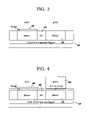
- an Si layer 20is formed and patterned to form shallow trench isolation (STI) 25 using standard techniques of pad oxidation, pad nitride deposition, lithography based patterning, reactive ion etching (RIE) of the stack consisting of nitride, oxide, and silicon down to the buried oxide, edge oxidation, liner deposition, fill deposition, and chemical mechanical polish.
- STIshallow trench isolation
- RIEreactive ion etching
- the STI formation processis well known in the art.
- high temperature stable amorphous materiale.g., SiO 2 , is used for the STI.
- an epitaxial Ge material (layer) 30is deposited over the surface of the structure using conventional techniques such as chemical vapor deposition methods.
- ultrahigh vacuum chemical vapor depositionUHVCVD
- RTCVDrapid thermal chemical vapor deposition
- LPCVDlimited reaction processing CVD
- MBEmolecular beam epitaxy
- the thickness of the Ge materialmay range from 5 to 50 nanometers, or other dimension depending on the thickness of the underlying Si layer which may, for example, range from 30 to 100 nanometers.
- nFET hard mask 35is provided on a portion of the Ge layer 30 (e.g., at locations of a yet to be formed nFET device).
- the nFET hard mask 35may be a nitride hard mask formed using a conventional deposition process such as spin-on coating, CVD, plasma-assisted CVD, ultrahigh vacuum chemical vapor deposition (UHVCVD), rapid thermal chemical vapor deposition (RTCVD), limited reaction processing CVD (LRPCVD) and other like deposition processes.
- the exposed Ge layer 30is etched and the nFET mask 35 is stripped using techniques known in the art.
- the Ge layer 30may be selectively etched using RIE, wet or dry etching.
- a Si:C material 40(or optionally C) is deposited on the structure, including over the epitaxially deposited Ge material 35 .
- ultrahigh vacuum chemical vapor depositionUHVCVD
- UHVCVDultrahigh vacuum chemical vapor deposition
- Other conventional techniquesinclude rapid thermal chemical vapor deposition (RTCVD), limited reaction processing CVD (LRPCVD) and other like processes.
- RTCVDrapid thermal chemical vapor deposition
- LPCVDlimited reaction processing CVD
- the thickness of the Si:C or C materialmay range from 5 to 50 nanometers, or other dimension depending on the thickness of the underlying Si layer which may, for example, range from 30 to 100 nanometers. In another aspect, when using C, the thickness may range from 1 to 30 nanometers.
- a pFET hard mask 45is provided on a portion of the Si:C material 40 at locations of the yet to be formed pFET.
- the pFET hard mask 45may be a nitride hard mask formed using a conventional deposition process such as spin-on coating, CVD, plasma-assisted CVD, ultrahigh vacuum chemical vapor deposition (UHVCVD), rapid thermal chemical vapor deposition (RTCVD), limited reaction processing CVD (LRPCVD) and other like deposition processes.
- the exposed Si:C layer 40is then etched and the pFET mask 45 is stripped using techniques known in the art.
- the Si:C and pFETmay be etched using standard etching techniques such as, for example, RIE, wet or dry etching and the like.
- the structurethen undergoes a thermal annealing process.
- the deposited Ge material 30is mixed into the underlying SOI film to form an island 50 of substantially SiGe material.
- the deposited Si:C or optional C materialis mixed into the underlying SOI film forming an island 55 of substantially Si:C material.
- the thermal annealing processtakes place, for example, at about 1200° C. to 1350° C. between 1 hour and 10 hours, with one implementation at 1200° C. for approximately 5 hours.
- the required Ge %is not large (e.g., less than 25% and in one implementation 10 to 20%) for the nFET and thus does not cause defect issues.
- the STI 25can relax and facilitate the relaxation of the SiGe island 50 and Si:C island 55 . This is due, in part, because the STI comprises oxide material, which is a viscous material at the high temperature, e.g., becomes a low viscosity material at high temperature.
- the SiGe island 50 and the Si:C island 55have different relaxed crystal lattice (different dimensions between the atoms) which yield a unique substrate with small crystal islands.
- the relaxation of the SiGe island 50 and the Si:C island 55provides improved performance as compared to blanket (SiGe or Si:C) substrates.
- high temperature stable amorphous materiale.g., SiO 2
- SiO 2high temperature stable amorphous material
- FIGS. 7–10show another aspect of the invention.
- a silicon wafersuch as SOI is shown.
- the SOImay be fabricated using the SIMOX process or other well known processes.
- An Si layer 20is patterned to form shallow trench isolation (STI) 25 using standard techniques of pad oxidation, pad nitride deposition, lithography based patterning, reactive ion etching (RIE) of the stack consisting of nitride, oxide, and silicon down to the buried oxide, edge oxidation, liner deposition, fill deposition, and chemical mechanical polish.
- STIshallow trench isolation
- the STI formation processis well known in the art.
- a pFET mask 40is provided on a portion of the structure at locations of the yet to be formed pFET.
- the pFET hard maskmay be deposited using convention techniques such as chemical vapor deposition methods.
- such techniquesmay include spin-on coating, CVD, plasma-assisted CVD, evaporation ultrahigh vacuum chemical vapor deposition (UHVCVD), rapid thermal chemical vapor deposition (RTCVD), limited reaction processing CVD (LRPCVD) and other like deposition processes.
- An epitaxial Ge layer 30is selectively grown over the exposed surface of the yet to be formed nFET using conventional techniques.
- the thickness of the Ge materialmay range from 5 to 50 nanometers, or other dimension depending on the thickness of the underlying Si layer which may, for example, range from 30 to 100 nanometers.
- the hard mask 45is stripped using well known processes, as discussed above.
- an nFET mask 35is provided on a portion of the structure at locations of the yet to be formed nFET.
- the nFET hard maskmay be deposited using conventional techniques such as chemical vapor deposition methods as discussed throughout and which should be known to those of ordinary skill.
- An Si:C layer 40is selectively grown over the exposed surface of the structure at the yet to be formed pFET using conventional techniques such as chemical vapor deposition method, as discussed above.
- the thickness of the Si:C materialmay range from 5 to 50 nanometers, or other dimension depending on the thickness of the underlying Si layer which may, for example, range from 30 to 100 nanometers.
- the Cmay even be thinner ranging from 1 to 50 nanometers.
- the nFET hard mask 35is then removed using well known processes.
- the structurethen undergoes a thermal annealing process.
- the annealing processfor the nFET device, the Ge material 30 is mixed into the SOI film forming an island 50 of substantially SiGe material.
- the Si:C or optionally C materialis mixed into the SOI film forming an island 55 of substantially Si:C material.
- This processalso forms a BOX layer, as the substrate.
- the thermal annealing processtakes place, for example, at about 1200° C. to 1350° C. between 1 hour and 10 hours, with one implementation at 1200° C. for approximately 5 hours.
- the required Ge %is not large (e.g., less than 25% and in one implementation from 10 to 20%) and thus does not cause defect issues.
- the STI 25can relax and facilitate the relaxation of the SiGe island 50 and Si:C island 55 .
- the relaxation of SiGe and Si:Cprovides improved performance as compared to blanket (SiGe or Si:C) substrates.
- the element of such structureis the use of high temperature stable amorphous material, e.g., SiO 2 , between the islands and the crystal on insulator structure.
- Ccan be implanted at high dose into the pFET region which can produce concentrations much greater than the 1–4% C in the Si:C upon thermal annealing.
- the dosemay be about 1 e 16 #/cm 2 or greater such as 5 e 16 #/cm 2 .
- the hard maskis nitride, and is deposited in any known conventional manner over the structure.
- the nitride hard maskmay be hard mask formed using a conventional deposition process such as spin-on coating, CVD, plasma-assisted CVD, ultrahigh vacuum chemical vapor deposition (UHVCVD), rapid thermal chemical vapor deposition (RTCVD), limited reaction processing CVD (LRPCVD) and other like deposition processes.
- the hard maskis deposited to a range from 5 to 50 nanometers, or other dimension depending on the thickness of the underlying layers.
- a sidewall image transfer and etchis performed in a conventional manner to form the fins 75 and 80 .
- the finsare defined by Sidewall-Image Transfer Lithography, which places fins on the perimeter of drawn rectangles (mandrels).
- a trim maskis used to remove undesired parts of loops and a conventional resist mask is used to block off source and drain regions (not shown) to link the fins together.
- the hard mask 70remains as a cap of the nFET and pFET regions.
- an Si epi layer 85is selectively grown on the sidewalls of the nFET and the pFET.
- the Si epi layermay grow asymmetrically thus possibly inducing buckling in the nFET due to its highly compressive state, as discussed below.
- the highly tensile hard maskwill ensure and even prevent such buckling by substantially equalizing the forces acting on the nFET region during the Si growth.
- the lattice constant of the Si epi sidewall layeris different than that of the SiGe and the Si:C “islands” or etched fins.
- the SiGehas a lattice constant a ⁇ aSi and the Si:C has a lattice constant a ⁇ aSi. That is, standing alone, the Si normally has a lower lattice constant than the SiGe layer; namely, the lattice constant of the Si material does not match the lattice constant of the SiGe layer.
- the lattice structure of the Si sidewall layerwill tend to match the lattice structure of the SiGe.
- the Si layeris placed under a tensile stress. This area will act as a strained channel for the nFET.
- the Ge content of the SiGe layermay be less than 25% in ratio to the Si content.
- the lattice structure of the Si layerwill tend to match the lattice structure of the Si:C.
- the Si layeris placed under a compressive stress. That is, similar to the occurrence with the SiGe, the surrounding areas of the Si:C island will try to obtain an equilibrium state thus resulting in a compressive stress of an epitaxial Si sidewall layer formed on the Si:C. This area will act as a strained channel for the pFET.
- the C contentmay be up to about 4% in ratio to the Si content.
- the structure formed, as shown in FIG. 13is an intermediate structure that accommodates formation of semiconductor devices, such as pFETs and nFETs, in accordance with the principles of the invention.
- CMOS processesmay be performed to form n and p finFET devices on the structure, as is well known in the finFET art.
- the devicesmay include ion implantation of source and drain regions separated by the semiconducting channel of strained SiGe and Si:C. That is, the nFET will be formed over the tensilely strained channel and the pFET will be formed over the compressively strained Si channel.
- a gate dielectricis provided atop the strained channel, and a gate conductor is provided on top of the gate dielectric.
Landscapes
- Metal-Oxide And Bipolar Metal-Oxide Semiconductor Integrated Circuits (AREA)
- Thin Film Transistor (AREA)
- Element Separation (AREA)
- Insulated Gate Type Field-Effect Transistor (AREA)
- Recrystallisation Techniques (AREA)
Abstract
Description
Claims (26)
Priority Applications (3)
| Application Number | Priority Date | Filing Date | Title |
|---|---|---|---|
| US10/733,378US7198995B2 (en) | 2003-12-12 | 2003-12-12 | Strained finFETs and method of manufacture |
| CNB2004100950072ACN100356525C (en) | 2003-12-12 | 2004-11-18 | Strained finFETs and method of manufacture |
| JP2004357623AJP4130652B2 (en) | 2003-12-12 | 2004-12-10 | Semiconductor structure and manufacturing method thereof |
Applications Claiming Priority (1)
| Application Number | Priority Date | Filing Date | Title |
|---|---|---|---|
| US10/733,378US7198995B2 (en) | 2003-12-12 | 2003-12-12 | Strained finFETs and method of manufacture |
Publications (2)
| Publication Number | Publication Date |
|---|---|
| US20050130358A1 US20050130358A1 (en) | 2005-06-16 |
| US7198995B2true US7198995B2 (en) | 2007-04-03 |
Family
ID=34653077
Family Applications (1)
| Application Number | Title | Priority Date | Filing Date |
|---|---|---|---|
| US10/733,378Expired - LifetimeUS7198995B2 (en) | 2003-12-12 | 2003-12-12 | Strained finFETs and method of manufacture |
Country Status (3)
| Country | Link |
|---|---|
| US (1) | US7198995B2 (en) |
| JP (1) | JP4130652B2 (en) |
| CN (1) | CN100356525C (en) |
Cited By (65)
| Publication number | Priority date | Publication date | Assignee | Title |
|---|---|---|---|---|
| US20080001169A1 (en)* | 2006-03-24 | 2008-01-03 | Amberwave Systems Corporation | Lattice-mismatched semiconductor structures and related methods for device fabrication |
| US20080073667A1 (en)* | 2006-09-27 | 2008-03-27 | Amberwave Systems Corporation | Tri-gate field-effect transistors formed by aspect ratio trapping |
| US20080206934A1 (en)* | 2007-02-23 | 2008-08-28 | Jones Robert E | Forming semiconductor fins using a sacrificial fin |
| US20080237709A1 (en)* | 2007-03-30 | 2008-10-02 | International Business Machines Corporation | After gate fabrication of field effect transistor having tensile and compressive regions |
| US20080257409A1 (en)* | 2007-04-09 | 2008-10-23 | Amberwave Systems Corporation | Photovoltaics on silicon |
| US20090079008A1 (en)* | 2007-09-21 | 2009-03-26 | Texas Instruments Incorporated | CMOS Fabrication Process |
| US20090085027A1 (en)* | 2007-09-29 | 2009-04-02 | Intel Corporation | Three dimensional strained quantum wells and three dimensional strained surface channels by ge confinement method |
| US20090250763A1 (en)* | 2007-08-23 | 2009-10-08 | Gerhard Knoblinger | Integrated circuit including a first channel and a second channel |
| US20100163842A1 (en)* | 2008-12-29 | 2010-07-01 | Li-Shyue Lai | Multiple-Gate Transistors with Reverse T-Shaped Fins |
| US20110180847A1 (en)* | 2010-01-22 | 2011-07-28 | Keiji Ikeda | Semiconductor device and fabrication method thereof |
| US8183627B2 (en) | 2004-12-01 | 2012-05-22 | Taiwan Semiconductor Manufacturing Company, Ltd. | Hybrid fin field-effect transistor structures and related methods |
| US8216951B2 (en) | 2006-09-27 | 2012-07-10 | Taiwan Semiconductor Manufacturing Company, Ltd. | Quantum tunneling devices and circuits with lattice-mismatched semiconductor structures |
| US8237151B2 (en) | 2009-01-09 | 2012-08-07 | Taiwan Semiconductor Manufacturing Company, Ltd. | Diode-based devices and methods for making the same |
| US8253211B2 (en) | 2008-09-24 | 2012-08-28 | Taiwan Semiconductor Manufacturing Company, Ltd. | Semiconductor sensor structures with reduced dislocation defect densities |
| US8274097B2 (en) | 2008-07-01 | 2012-09-25 | Taiwan Semiconductor Manufacturing Company, Ltd. | Reduction of edge effects from aspect ratio trapping |
| US8304805B2 (en) | 2009-01-09 | 2012-11-06 | Taiwan Semiconductor Manufacturing Company, Ltd. | Semiconductor diodes fabricated by aspect ratio trapping with coalesced films |
| US8324660B2 (en) | 2005-05-17 | 2012-12-04 | Taiwan Semiconductor Manufacturing Company, Ltd. | Lattice-mismatched semiconductor structures with reduced dislocation defect densities and related methods for device fabrication |
| US8329541B2 (en) | 2007-06-15 | 2012-12-11 | Taiwan Semiconductor Manufacturing Company, Ltd. | InP-based transistor fabrication |
| US8344242B2 (en) | 2007-09-07 | 2013-01-01 | Taiwan Semiconductor Manufacturing Company, Ltd. | Multi-junction solar cells |
| US8384196B2 (en) | 2008-09-19 | 2013-02-26 | Taiwan Semiconductor Manufacturing Company, Ltd. | Formation of devices by epitaxial layer overgrowth |
| US8502263B2 (en) | 2006-10-19 | 2013-08-06 | Taiwan Semiconductor Manufacturing Company, Ltd. | Light-emitter-based devices with lattice-mismatched semiconductor structures |
| US8551845B2 (en) | 2010-09-21 | 2013-10-08 | International Business Machines Corporation | Structure and method for increasing strain in a device |
| US8624103B2 (en) | 2007-04-09 | 2014-01-07 | Taiwan Semiconductor Manufacturing Company, Ltd. | Nitride-based multi-junction solar cell modules and methods for making the same |
| US8629446B2 (en) | 2009-04-02 | 2014-01-14 | Taiwan Semiconductor Manufacturing Company, Ltd. | Devices formed from a non-polar plane of a crystalline material and method of making the same |
| US8680576B2 (en)* | 2012-05-16 | 2014-03-25 | Taiwan Semiconductor Manufacturing Company, Ltd. | CMOS device and method of forming the same |
| US8697523B2 (en) | 2012-02-06 | 2014-04-15 | International Business Machines Corporation | Integration of SMT in replacement gate FINFET process flow |
| US20140103366A1 (en)* | 2003-11-19 | 2014-04-17 | International Business Machines Corporation | Silicon device on si:c-oi and sgoi and method of manufacture |
| US8815670B2 (en) | 2012-12-07 | 2014-08-26 | International Business Machines Corporation | Preventing Fin erosion and limiting EPI overburden in FinFET structures by composite hardmask |
| US8822248B2 (en) | 2008-06-03 | 2014-09-02 | Taiwan Semiconductor Manufacturing Company, Ltd. | Epitaxial growth of crystalline material |
| US20140264602A1 (en)* | 2013-03-14 | 2014-09-18 | International Business Machines Corporation | Forming strained and relaxed silicon and silicon germanium fins on the same wafer |
| US8841178B1 (en) | 2013-03-13 | 2014-09-23 | International Business Machines Corporation | Strained silicon nFET and silicon germanium pFET on same wafer |
| US8847279B2 (en) | 2006-09-07 | 2014-09-30 | Taiwan Semiconductor Manufacturing Company, Ltd. | Defect reduction using aspect ratio trapping |
| US8853750B2 (en) | 2012-04-27 | 2014-10-07 | International Business Machines Corporation | FinFET with enhanced embedded stressor |
| US8889495B2 (en) | 2012-10-04 | 2014-11-18 | International Business Machines Corporation | Semiconductor alloy fin field effect transistor |
| US8895395B1 (en) | 2013-06-06 | 2014-11-25 | International Business Machines Corporation | Reduced resistance SiGe FinFET devices and method of forming same |
| US8981427B2 (en) | 2008-07-15 | 2015-03-17 | Taiwan Semiconductor Manufacturing Company, Ltd. | Polishing of small composite semiconductor materials |
| US8987069B1 (en) | 2013-12-04 | 2015-03-24 | International Business Machines Corporation | Semiconductor substrate with multiple SiGe regions having different germanium concentrations by a single epitaxy process |
| US9040363B2 (en) | 2013-03-20 | 2015-05-26 | International Business Machines Corporation | FinFET with reduced capacitance |
| US20150255457A1 (en)* | 2014-03-04 | 2015-09-10 | International Business Machines Corporation | Methods and apparatus to form fin structures of different compositions on a same wafer via mandrel and diffusion |
| US9293375B2 (en) | 2014-04-24 | 2016-03-22 | International Business Machines Corporation | Selectively grown self-aligned fins for deep isolation integration |
| US9324623B1 (en) | 2014-11-26 | 2016-04-26 | Samsung Electronics Co., Ltd. | Method of manufacturing semiconductor device having active fins |
| US9362182B2 (en) | 2014-11-06 | 2016-06-07 | International Business Machines Corporation | Forming strained fins of different material on a substrate |
| US9401372B1 (en) | 2015-02-10 | 2016-07-26 | International Business Machines Corporation | Dual isolation on SSOI wafer |
| US9431486B1 (en)* | 2015-11-30 | 2016-08-30 | International Business Machines Corporation | Channel strain and controlling lateral epitaxial growth of the source and drain in FinFET devices |
| US9484201B2 (en) | 2015-02-23 | 2016-11-01 | International Business Machines Corporation | Epitaxial silicon germanium fin formation using sacrificial silicon fin templates |
| US9496185B2 (en) | 2015-03-27 | 2016-11-15 | International Business Machines Corporation | Dual channel finFET with relaxed pFET region |
| US9508741B2 (en) | 2015-02-10 | 2016-11-29 | International Business Machines Corporation | CMOS structure on SSOI wafer |
| US9548386B1 (en) | 2015-08-31 | 2017-01-17 | International Business Machines Corporation | Structure and method for compressively strained silicon germanium fins for pFET devices and tensily strained silicon fins for nFET devices |
| US9564367B2 (en)* | 2012-09-13 | 2017-02-07 | Globalfoundries Inc. | Methods of forming different FinFET devices with different threshold voltages and integrated circuit products containing such devices |
| US9570360B2 (en) | 2014-08-27 | 2017-02-14 | International Business Machines Corporation | Dual channel material for finFET for high performance CMOS |
| US9660081B2 (en) | 2014-02-28 | 2017-05-23 | Stmicroelectronics, Inc. | Method to form localized relaxed substrate by using condensation |
| US9660035B2 (en) | 2014-01-29 | 2017-05-23 | International Business Machines Corporation | Semiconductor device including superlattice SiGe/Si fin structure |
| US9768299B2 (en) | 2014-02-21 | 2017-09-19 | Stmicroelectronics Inc. | Method to form strained channel in thin box SOI structures by elastic strain relaxation of the substrate |
| US9773870B1 (en) | 2016-06-28 | 2017-09-26 | International Business Machines Corporation | Strained semiconductor device |
| US20170372970A1 (en)* | 2016-06-09 | 2017-12-28 | International Business Machines Corporation | Forming insulator fin structure in isolation region to support gate structures |
| US9859426B1 (en) | 2016-06-29 | 2018-01-02 | International Business Machines Corporation | Semiconductor device including optimized elastic strain buffer |
| US9859381B2 (en) | 2005-05-17 | 2018-01-02 | Taiwan Semiconductor Manufacturing Company, Ltd. | Lattice-mismatched semiconductor structures with reduced dislocation defect densities and related methods for device fabrication |
| US9917019B2 (en)* | 2015-08-20 | 2018-03-13 | International Business Machines Corporation | Strained FinFET device fabrication |
| US9917154B2 (en) | 2016-06-29 | 2018-03-13 | International Business Machines Corporation | Strained and unstrained semiconductor device features formed on the same substrate |
| US9984872B2 (en) | 2008-09-19 | 2018-05-29 | Taiwan Semiconductor Manufacturing Company, Ltd. | Fabrication and structures of crystalline material |
| US10438855B2 (en) | 2017-02-17 | 2019-10-08 | International Business Machines Corporation | Dual channel FinFETs having uniform fin heights |
| US10622352B2 (en) | 2017-01-25 | 2020-04-14 | International Business Machines Corporation | Fin cut to prevent replacement gate collapse on STI |
| US10886367B2 (en) | 2019-01-17 | 2021-01-05 | International Business Machines Corporation | Forming FinFET with reduced variability |
| US10910276B1 (en) | 2019-10-01 | 2021-02-02 | Globalfoundries Inc. | STI structure with liner along lower portion of longitudinal sides of active region, and related FET and method |
| US11342441B2 (en) | 2012-07-17 | 2022-05-24 | Unm Rainforest Innovations | Method of forming a seed area and growing a heteroepitaxial layer on the seed area |
Families Citing this family (44)
| Publication number | Priority date | Publication date | Assignee | Title |
|---|---|---|---|---|
| US7532501B2 (en)* | 2005-06-02 | 2009-05-12 | International Business Machines Corporation | Semiconductor device including back-gated transistors and method of fabricating the device |
| US20070018239A1 (en)* | 2005-07-20 | 2007-01-25 | International Business Machines Corporation | Sea-of-fins structure on a semiconductor substrate and method of fabrication |
| US7655511B2 (en) | 2005-11-03 | 2010-02-02 | International Business Machines Corporation | Gate electrode stress control for finFET performance enhancement |
| US7510939B2 (en)* | 2006-01-31 | 2009-03-31 | International Business Machines Corporation | Microelectronic structure by selective deposition |
| US7365401B2 (en)* | 2006-03-28 | 2008-04-29 | International Business Machines Corporation | Dual-plane complementary metal oxide semiconductor |
| US20070238267A1 (en)* | 2006-03-28 | 2007-10-11 | International Business Machines Corporation | Epitaxy of Silicon-Carbon Substitutional Solid Solutions by Ultra-Fast Annealing of Amorphous Material |
| US7681628B2 (en)* | 2006-04-12 | 2010-03-23 | International Business Machines Corporation | Dynamic control of back gate bias in a FinFET SRAM cell |
| US8227316B2 (en)* | 2006-06-29 | 2012-07-24 | International Business Machines Corporation | Method for manufacturing double gate finFET with asymmetric halo |
| US7462916B2 (en)* | 2006-07-19 | 2008-12-09 | International Business Machines Corporation | Semiconductor devices having torsional stresses |
| US7462522B2 (en)* | 2006-08-30 | 2008-12-09 | International Business Machines Corporation | Method and structure for improving device performance variation in dual stress liner technology |
| JP2008060408A (en)* | 2006-08-31 | 2008-03-13 | Toshiba Corp | Semiconductor device |
| US7829407B2 (en) | 2006-11-20 | 2010-11-09 | International Business Machines Corporation | Method of fabricating a stressed MOSFET by bending SOI region |
| US8217423B2 (en) | 2007-01-04 | 2012-07-10 | International Business Machines Corporation | Structure and method for mobility enhanced MOSFETs with unalloyed silicide |
| JP2010118621A (en)* | 2008-11-14 | 2010-05-27 | Nec Electronics Corp | Semiconductor device, and method of manufacturing the same |
| US9768305B2 (en)* | 2009-05-29 | 2017-09-19 | Taiwan Semiconductor Manufacturing Company, Ltd. | Gradient ternary or quaternary multiple-gate transistor |
| US20120146101A1 (en)* | 2010-12-13 | 2012-06-14 | Chun-Hsien Lin | Multi-gate transistor devices and manufacturing method thereof |
| CN103065963B (en)* | 2011-10-19 | 2015-08-05 | 中芯国际集成电路制造(上海)有限公司 | fin transistor and forming method thereof |
| US9048136B2 (en) | 2011-10-26 | 2015-06-02 | GlobalFoundries, Inc. | SRAM cell with individual electrical device threshold control |
| US9029956B2 (en) | 2011-10-26 | 2015-05-12 | Global Foundries, Inc. | SRAM cell with individual electrical device threshold control |
| CN103107192B (en)* | 2011-11-10 | 2016-05-18 | 中芯国际集成电路制造(北京)有限公司 | Semiconductor device and manufacture method thereof |
| CN103107187B (en)* | 2011-11-10 | 2016-04-13 | 中芯国际集成电路制造(北京)有限公司 | The manufacture method of semiconductor device |
| CN103165455B (en)* | 2011-12-13 | 2015-09-09 | 中芯国际集成电路制造(上海)有限公司 | Make the method for fin-shaped field effect transistor |
| KR101700213B1 (en)* | 2011-12-21 | 2017-01-26 | 인텔 코포레이션 | Methods for forming fins for metal oxide semiconductor device structures |
| US20130200459A1 (en) | 2012-02-02 | 2013-08-08 | International Business Machines Corporation | Strained channel for depleted channel semiconductor devices |
| CN103367253B (en)* | 2012-03-29 | 2015-03-11 | 中芯国际集成电路制造(上海)有限公司 | Fin type field effect transistor forming method |
| US9029835B2 (en)* | 2012-12-20 | 2015-05-12 | Intel Corporation | Epitaxial film on nanoscale structure |
| US9184233B2 (en)* | 2013-02-27 | 2015-11-10 | Taiwan Semiconductor Manufacturing Company, Ltd. | Structure and method for defect passivation to reduce junction leakage for finFET device |
| US8933528B2 (en)* | 2013-03-11 | 2015-01-13 | International Business Machines Corporation | Semiconductor fin isolation by a well trapping fin portion |
| US8829606B1 (en)* | 2013-03-13 | 2014-09-09 | Taiwan Semiconductor Manufacturing Company, Ltd. | Ditches near semiconductor fins and methods for forming the same |
| US9093275B2 (en)* | 2013-10-22 | 2015-07-28 | International Business Machines Corporation | Multi-height multi-composition semiconductor fins |
| US9165929B2 (en)* | 2013-11-25 | 2015-10-20 | Qualcomm Incorporated | Complementarily strained FinFET structure |
| US9129863B2 (en)* | 2014-02-11 | 2015-09-08 | International Business Machines Corporation | Method to form dual channel group III-V and Si/Ge FINFET CMOS |
| US9123585B1 (en) | 2014-02-11 | 2015-09-01 | International Business Machines Corporation | Method to form group III-V and Si/Ge FINFET on insulator |
| US20150340501A1 (en)* | 2014-05-22 | 2015-11-26 | Globalfoundries Inc. | Forming independent-gate finfet with tilted pre-amorphization implantation and resulting device |
| US9536900B2 (en)* | 2014-05-22 | 2017-01-03 | Globalfoundries Inc. | Forming fins of different semiconductor materials on the same substrate |
| US9607901B2 (en) | 2015-05-06 | 2017-03-28 | Stmicroelectronics, Inc. | Integrated tensile strained silicon NFET and compressive strained silicon-germanium PFET implemented in FINFET technology |
| US9613871B2 (en) | 2015-07-16 | 2017-04-04 | Samsung Electronics Co., Ltd. | Semiconductor device and fabricating method thereof |
| US9741581B2 (en)* | 2016-01-11 | 2017-08-22 | Globalfoundries Inc. | Using tensile mask to minimize buckling in substrate |
| WO2018063372A1 (en)* | 2016-09-30 | 2018-04-05 | Intel Corporation | Supperlatice channel included in a trench |
| EP4053880A1 (en)* | 2018-04-22 | 2022-09-07 | Epinovatech AB | Reinforced thin-film device |
| CN110571195B (en)* | 2018-06-05 | 2021-12-21 | 中芯国际集成电路制造(上海)有限公司 | SRAM (static random Access memory), manufacturing method thereof and electronic device |
| US10861969B2 (en)* | 2018-07-16 | 2020-12-08 | Taiwan Semiconductor Manufacturing Co., Ltd. | Method of forming FinFET structure with reduced Fin buckling |
| US11670551B2 (en)* | 2019-09-26 | 2023-06-06 | Taiwan Semiconductor Manufacturing Co., Ltd. | Interface trap charge density reduction |
| US11257932B2 (en)* | 2020-01-30 | 2022-02-22 | Taiwan Semiconductor Manufacturing Co., Ltd. | Fin field effect transistor device structure and method for forming the same |
Citations (94)
| Publication number | Priority date | Publication date | Assignee | Title |
|---|---|---|---|---|
| US3602841A (en) | 1970-06-18 | 1971-08-31 | Ibm | High frequency bulk semiconductor amplifiers and oscillators |
| US4665415A (en) | 1985-04-24 | 1987-05-12 | International Business Machines Corporation | Semiconductor device with hole conduction via strained lattice |
| JPS6476755A (en) | 1987-09-18 | 1989-03-22 | Hitachi Ltd | Semiconductor device |
| US4853076A (en) | 1983-12-29 | 1989-08-01 | Massachusetts Institute Of Technology | Semiconductor thin films |
| US4855245A (en) | 1985-09-13 | 1989-08-08 | Siemens Aktiengesellschaft | Method of manufacturing integrated circuit containing bipolar and complementary MOS transistors on a common substrate |
| US4952524A (en) | 1989-05-05 | 1990-08-28 | At&T Bell Laboratories | Semiconductor device manufacture including trench formation |
| US4958213A (en) | 1987-12-07 | 1990-09-18 | Texas Instruments Incorporated | Method for forming a transistor base region under thick oxide |
| US5006913A (en) | 1988-11-05 | 1991-04-09 | Mitsubishi Denki Kabushiki Kaisha | Stacked type semiconductor device |
| US5060030A (en) | 1990-07-18 | 1991-10-22 | Raytheon Company | Pseudomorphic HEMT having strained compensation layer |
| US5081513A (en) | 1991-02-28 | 1992-01-14 | Xerox Corporation | Electronic device with recovery layer proximate to active layer |
| US5108843A (en) | 1988-11-30 | 1992-04-28 | Ricoh Company, Ltd. | Thin film semiconductor and process for producing the same |
| US5134085A (en) | 1991-11-21 | 1992-07-28 | Micron Technology, Inc. | Reduced-mask, split-polysilicon CMOS process, incorporating stacked-capacitor cells, for fabricating multi-megabit dynamic random access memories |
| US5310446A (en) | 1990-01-10 | 1994-05-10 | Ricoh Company, Ltd. | Method for producing semiconductor film |
| US5354695A (en) | 1992-04-08 | 1994-10-11 | Leedy Glenn J | Membrane dielectric isolation IC fabrication |
| US5371399A (en) | 1991-06-14 | 1994-12-06 | International Business Machines Corporation | Compound semiconductor having metallic inclusions and devices fabricated therefrom |
| US5391510A (en) | 1992-02-28 | 1995-02-21 | International Business Machines Corporation | Formation of self-aligned metal gate FETs using a benignant removable gate material during high temperature steps |
| US5459346A (en) | 1988-06-28 | 1995-10-17 | Ricoh Co., Ltd. | Semiconductor substrate with electrical contact in groove |
| US5557122A (en) | 1995-05-12 | 1996-09-17 | Alliance Semiconductors Corporation | Semiconductor electrode having improved grain structure and oxide growth properties |
| US5561302A (en) | 1994-09-26 | 1996-10-01 | Motorola, Inc. | Enhanced mobility MOSFET device and method |
| US5670798A (en) | 1995-03-29 | 1997-09-23 | North Carolina State University | Integrated heterostructures of Group III-V nitride semiconductor materials including epitaxial ohmic contact non-nitride buffer layer and methods of fabricating same |
| US5679965A (en) | 1995-03-29 | 1997-10-21 | North Carolina State University | Integrated heterostructures of Group III-V nitride semiconductor materials including epitaxial ohmic contact, non-nitride buffer layer and methods of fabricating same |
| US5861651A (en) | 1997-02-28 | 1999-01-19 | Lucent Technologies Inc. | Field effect devices and capacitors with improved thin film dielectrics and method for making same |
| US5880040A (en) | 1996-04-15 | 1999-03-09 | Macronix International Co., Ltd. | Gate dielectric based on oxynitride grown in N2 O and annealed in NO |
| US5940736A (en) | 1997-03-11 | 1999-08-17 | Lucent Technologies Inc. | Method for forming a high quality ultrathin gate oxide layer |
| US5940716A (en) | 1996-03-15 | 1999-08-17 | Samsung Electronics Co., Ltd. | Methods of forming trench isolation regions using repatterned trench masks |
| US5960297A (en) | 1997-07-02 | 1999-09-28 | Kabushiki Kaisha Toshiba | Shallow trench isolation structure and method of forming the same |
| US5981356A (en) | 1997-07-28 | 1999-11-09 | Integrated Device Technology, Inc. | Isolation trenches with protected corners |
| US5989978A (en) | 1998-07-16 | 1999-11-23 | Chartered Semiconductor Manufacturing, Ltd. | Shallow trench isolation of MOSFETS with reduced corner parasitic currents |
| US6008126A (en) | 1992-04-08 | 1999-12-28 | Elm Technology Corporation | Membrane dielectric isolation IC fabrication |
| US6025280A (en) | 1997-04-28 | 2000-02-15 | Lucent Technologies Inc. | Use of SiD4 for deposition of ultra thin and controllable oxides |
| US6066545A (en) | 1997-12-09 | 2000-05-23 | Texas Instruments Incorporated | Birdsbeak encroachment using combination of wet and dry etch for isolation nitride |
| US6080637A (en) | 1998-12-07 | 2000-06-27 | Taiwan Semiconductor Manufacturing Company | Shallow trench isolation technology to eliminate a kink effect |
| US6090684A (en) | 1998-07-31 | 2000-07-18 | Hitachi, Ltd. | Method for manufacturing semiconductor device |
| US6093621A (en) | 1999-04-05 | 2000-07-25 | Vanguard International Semiconductor Corp. | Method of forming shallow trench isolation |
| US6107143A (en) | 1998-03-02 | 2000-08-22 | Samsung Electronics Co., Ltd. | Method for forming a trench isolation structure in an integrated circuit |
| US6117722A (en) | 1999-02-18 | 2000-09-12 | Taiwan Semiconductor Manufacturing Company | SRAM layout for relaxing mechanical stress in shallow trench isolation technology and method of manufacture thereof |
| US6133071A (en) | 1997-10-15 | 2000-10-17 | Nec Corporation | Semiconductor device with plate heat sink free from cracks due to thermal stress and process for assembling it with package |
| US6165383A (en) | 1998-04-10 | 2000-12-26 | Organic Display Technology | Useful precursors for organic electroluminescent materials and devices made from such materials |
| US6221735B1 (en) | 2000-02-15 | 2001-04-24 | Philips Semiconductors, Inc. | Method for eliminating stress induced dislocations in CMOS devices |
| US6228694B1 (en) | 1999-06-28 | 2001-05-08 | Intel Corporation | Method of increasing the mobility of MOS transistors by use of localized stress regions |
| US6255169B1 (en) | 1999-02-22 | 2001-07-03 | Advanced Micro Devices, Inc. | Process for fabricating a high-endurance non-volatile memory device |
| US6261964B1 (en) | 1997-03-14 | 2001-07-17 | Micron Technology, Inc. | Material removal method for forming a structure |
| US6265317B1 (en) | 2001-01-09 | 2001-07-24 | Taiwan Semiconductor Manufacturing Company | Top corner rounding for shallow trench isolation |
| US20010009784A1 (en) | 1998-01-09 | 2001-07-26 | Yanjun Ma | Structure and method of making a sub-micron MOS transistor |
| US6274444B1 (en) | 1999-07-30 | 2001-08-14 | United Microelectronics Corp. | Method for forming mosfet |
| US6281532B1 (en) | 1999-06-28 | 2001-08-28 | Intel Corporation | Technique to obtain increased channel mobilities in NMOS transistors by gate electrode engineering |
| US6284623B1 (en) | 1999-10-25 | 2001-09-04 | Peng-Fei Zhang | Method of fabricating semiconductor devices using shallow trench isolation with reduced narrow channel effect |
| US6284626B1 (en) | 1999-04-06 | 2001-09-04 | Vantis Corporation | Angled nitrogen ion implantation for minimizing mechanical stress on side walls of an isolation trench |
| US6319794B1 (en) | 1998-10-14 | 2001-11-20 | International Business Machines Corporation | Structure and method for producing low leakage isolation devices |
| US6361885B1 (en) | 1998-04-10 | 2002-03-26 | Organic Display Technology | Organic electroluminescent materials and device made from such materials |
| US6362082B1 (en) | 1999-06-28 | 2002-03-26 | Intel Corporation | Methodology for control of short channel effects in MOS transistors |
| US6368931B1 (en) | 2000-03-27 | 2002-04-09 | Intel Corporation | Thin tensile layers in shallow trench isolation and method of making same |
| US20020063292A1 (en) | 2000-11-29 | 2002-05-30 | Mark Armstrong | CMOS fabrication process utilizing special transistor orientation |
| US6403486B1 (en) | 2001-04-30 | 2002-06-11 | Taiwan Semiconductor Manufacturing Company | Method for forming a shallow trench isolation |
| US6403975B1 (en) | 1996-04-09 | 2002-06-11 | Max-Planck Gesellschaft Zur Forderung Der Wissenschafteneev | Semiconductor components, in particular photodetectors, light emitting diodes, optical modulators and waveguides with multilayer structures grown on silicon substrates |
| US6406973B1 (en) | 1999-06-29 | 2002-06-18 | Hyundai Electronics Industries Co., Ltd. | Transistor in a semiconductor device and method of manufacturing the same |
| US6413802B1 (en)* | 2000-10-23 | 2002-07-02 | The Regents Of The University Of California | Finfet transistor structures having a double gate channel extending vertically from a substrate and methods of manufacture |
| US20020086497A1 (en) | 2000-12-30 | 2002-07-04 | Kwok Siang Ping | Beaker shape trench with nitride pull-back for STI |
| US20020086472A1 (en) | 2000-12-29 | 2002-07-04 | Brian Roberds | Technique to obtain high mobility channels in MOS transistors by forming a strain layer on an underside of a channel |
| US20020090791A1 (en) | 1999-06-28 | 2002-07-11 | Brian S. Doyle | Method for reduced capacitance interconnect system using gaseous implants into the ild |
| US6461936B1 (en) | 2002-01-04 | 2002-10-08 | Infineon Technologies Ag | Double pullback method of filling an isolation trench |
| US6476462B2 (en) | 1999-12-28 | 2002-11-05 | Texas Instruments Incorporated | MOS-type semiconductor device and method for making same |
| US6483171B1 (en) | 1999-08-13 | 2002-11-19 | Micron Technology, Inc. | Vertical sub-micron CMOS transistors on (110), (111), (311), (511), and higher order surfaces of bulk, SOI and thin film structures and method of forming same |
| US6493497B1 (en) | 2000-09-26 | 2002-12-10 | Motorola, Inc. | Electro-optic structure and process for fabricating same |
| US6498358B1 (en) | 2001-07-20 | 2002-12-24 | Motorola, Inc. | Structure and method for fabricating an electro-optic system having an electrochromic diffraction grating |
| US6501121B1 (en) | 2000-11-15 | 2002-12-31 | Motorola, Inc. | Semiconductor structure |
| US6506652B2 (en) | 1998-11-13 | 2003-01-14 | Intel Corporation | Method of recessing spacers to improved salicide resistance on polysilicon gates |
| US20030032261A1 (en) | 2001-08-08 | 2003-02-13 | Ling-Yen Yeh | Method of preventing threshold voltage of MOS transistor from being decreased by shallow trench isolation formation |
| US20030040158A1 (en) | 2001-08-21 | 2003-02-27 | Nec Corporation | Semiconductor device and method of fabricating the same |
| US6531740B2 (en) | 2001-07-17 | 2003-03-11 | Motorola, Inc. | Integrated impedance matching and stability network |
| US6531369B1 (en) | 2000-03-01 | 2003-03-11 | Applied Micro Circuits Corporation | Heterojunction bipolar transistor (HBT) fabrication using a selectively deposited silicon germanium (SiGe) |
| US20030057184A1 (en) | 2001-09-22 | 2003-03-27 | Shiuh-Sheng Yu | Method for pull back SiN to increase rounding effect in a shallow trench isolation process |
| US20030067035A1 (en) | 2001-09-28 | 2003-04-10 | Helmut Tews | Gate processing method with reduced gate oxide corner and edge thinning |
| US6583060B2 (en) | 2001-07-13 | 2003-06-24 | Micron Technology, Inc. | Dual depth trench isolation |
| US6717216B1 (en) | 2002-12-12 | 2004-04-06 | International Business Machines Corporation | SOI based field effect transistor having a compressive film in undercut area under the channel and a method of making the device |
| US6803631B2 (en)* | 2003-01-23 | 2004-10-12 | Advanced Micro Devices, Inc. | Strained channel finfet |
| US6825529B2 (en) | 2002-12-12 | 2004-11-30 | International Business Machines Corporation | Stress inducing spacers |
| US20040238914A1 (en) | 2003-05-30 | 2004-12-02 | International Business Machines Corporation | STI stress modification by nitrogen plasma treatment for improving performance in small width devices |
| US6831292B2 (en) | 2001-09-21 | 2004-12-14 | Amberwave Systems Corporation | Semiconductor structures employing strained material layers with defined impurity gradients and methods for fabricating same |
| US20040262784A1 (en) | 2003-06-30 | 2004-12-30 | International Business Machines Corporation | High performance cmos device structures and method of manufacture |
| US6852576B2 (en)* | 2003-04-03 | 2005-02-08 | Advanced Micro Devices, Inc. | Method for forming structures in finfet devices |
| US20050048727A1 (en)* | 2003-09-03 | 2005-03-03 | Advanced Micro Devices, Inc. | Formation of finfet using a sidewall epitaxial layer |
| US20050082634A1 (en) | 2003-10-16 | 2005-04-21 | International Business Machines Corporation | High performance strained cmos devices |
| US20050093030A1 (en) | 2003-10-30 | 2005-05-05 | Doris Bruce B. | Structure and method to enhance both nFET and pFET performance using different kinds of stressed layers |
| US20050098829A1 (en) | 2003-11-06 | 2005-05-12 | Doris Bruce B. | High mobility CMOS circuits |
| US20050106799A1 (en) | 2003-11-14 | 2005-05-19 | International Business Machines Corporation | Stressed semiconductor device structures having granular semiconductor material |
| US20050145954A1 (en) | 2004-01-05 | 2005-07-07 | International Business Machines Corporation | Structures and methods for making strained mosfets |
| US20050161711A1 (en)* | 2003-05-01 | 2005-07-28 | International Business Machines Corporation | High performance FET devices and methods thereof |
| US20050194699A1 (en) | 2004-03-03 | 2005-09-08 | International Business Machines Corporation | Mobility enhanced cmos devices |
| US20050236668A1 (en) | 2004-04-23 | 2005-10-27 | International Business Machines Corporation | STRUCTURES AND METHODS FOR MANUFACTURING OF DISLOCATION FREE STRESSED CHANNELS IN BULK SILICON AND SOI CMOS DEVICES BY GATE STRESS ENGINEERING WITH SiGe AND/OR Si:C |
| US20050245017A1 (en) | 2003-10-30 | 2005-11-03 | Belyansky Michael P | Structure and method to improve channel mobility by gate electrode stress modification |
| US6974981B2 (en) | 2002-12-12 | 2005-12-13 | International Business Machines Corporation | Isolation structures for imposing stress patterns |
| US20060057787A1 (en) | 2002-11-25 | 2006-03-16 | Doris Bruce B | Strained finfet cmos device structures |
| US20060060925A1 (en) | 2004-09-17 | 2006-03-23 | International Business Machines Corporation | Semiconductor device structure with active regions having different surface directions and methods |
Family Cites Families (8)
| Publication number | Priority date | Publication date | Assignee | Title |
|---|---|---|---|---|
| US57184A (en)* | 1866-08-14 | Improved alloy | ||
| US32261A (en)* | 1861-05-07 | Bukial-case | ||
| US9784A (en)* | 1853-06-14 | Fergus burden | ||
| US67035A (en)* | 1867-07-23 | Improvement in tunnels | ||
| US86497A (en)* | 1869-02-02 | Improvement in machine for making cord | ||
| US5825529A (en)* | 1996-06-27 | 1998-10-20 | Xerox Corporation | Gyricon display with no elastomer substrate |
| US6657259B2 (en)* | 2001-12-04 | 2003-12-02 | International Business Machines Corporation | Multiple-plane FinFET CMOS |
| US6657252B2 (en)* | 2002-03-19 | 2003-12-02 | International Business Machines Corporation | FinFET CMOS with NVRAM capability |
- 2003
- 2003-12-12USUS10/733,378patent/US7198995B2/ennot_activeExpired - Lifetime
- 2004
- 2004-11-18CNCNB2004100950072Apatent/CN100356525C/ennot_activeExpired - Lifetime
- 2004-12-10JPJP2004357623Apatent/JP4130652B2/ennot_activeExpired - Fee Related
Patent Citations (114)
| Publication number | Priority date | Publication date | Assignee | Title |
|---|---|---|---|---|
| US3602841A (en) | 1970-06-18 | 1971-08-31 | Ibm | High frequency bulk semiconductor amplifiers and oscillators |
| US4853076A (en) | 1983-12-29 | 1989-08-01 | Massachusetts Institute Of Technology | Semiconductor thin films |
| US4665415A (en) | 1985-04-24 | 1987-05-12 | International Business Machines Corporation | Semiconductor device with hole conduction via strained lattice |
| US4855245A (en) | 1985-09-13 | 1989-08-08 | Siemens Aktiengesellschaft | Method of manufacturing integrated circuit containing bipolar and complementary MOS transistors on a common substrate |
| JPS6476755A (en) | 1987-09-18 | 1989-03-22 | Hitachi Ltd | Semiconductor device |
| US4958213A (en) | 1987-12-07 | 1990-09-18 | Texas Instruments Incorporated | Method for forming a transistor base region under thick oxide |
| US5565697A (en) | 1988-06-28 | 1996-10-15 | Ricoh Company, Ltd. | Semiconductor structure having island forming grooves |
| US5459346A (en) | 1988-06-28 | 1995-10-17 | Ricoh Co., Ltd. | Semiconductor substrate with electrical contact in groove |
| US5006913A (en) | 1988-11-05 | 1991-04-09 | Mitsubishi Denki Kabushiki Kaisha | Stacked type semiconductor device |
| US5108843A (en) | 1988-11-30 | 1992-04-28 | Ricoh Company, Ltd. | Thin film semiconductor and process for producing the same |
| US4952524A (en) | 1989-05-05 | 1990-08-28 | At&T Bell Laboratories | Semiconductor device manufacture including trench formation |
| US5310446A (en) | 1990-01-10 | 1994-05-10 | Ricoh Company, Ltd. | Method for producing semiconductor film |
| US5060030A (en) | 1990-07-18 | 1991-10-22 | Raytheon Company | Pseudomorphic HEMT having strained compensation layer |
| US5081513A (en) | 1991-02-28 | 1992-01-14 | Xerox Corporation | Electronic device with recovery layer proximate to active layer |
| US5371399A (en) | 1991-06-14 | 1994-12-06 | International Business Machines Corporation | Compound semiconductor having metallic inclusions and devices fabricated therefrom |
| US5471948A (en) | 1991-06-14 | 1995-12-05 | International Business Machines Corporation | Method of making a compound semiconductor having metallic inclusions |
| US5134085A (en) | 1991-11-21 | 1992-07-28 | Micron Technology, Inc. | Reduced-mask, split-polysilicon CMOS process, incorporating stacked-capacitor cells, for fabricating multi-megabit dynamic random access memories |
| US5391510A (en) | 1992-02-28 | 1995-02-21 | International Business Machines Corporation | Formation of self-aligned metal gate FETs using a benignant removable gate material during high temperature steps |
| US6008126A (en) | 1992-04-08 | 1999-12-28 | Elm Technology Corporation | Membrane dielectric isolation IC fabrication |
| US5354695A (en) | 1992-04-08 | 1994-10-11 | Leedy Glenn J | Membrane dielectric isolation IC fabrication |
| US5946559A (en) | 1992-04-08 | 1999-08-31 | Elm Technology Corporation | Membrane dielectric isolation IC fabrication |
| US5571741A (en) | 1992-04-08 | 1996-11-05 | Leedy; Glenn J. | Membrane dielectric isolation IC fabrication |
| US5592018A (en) | 1992-04-08 | 1997-01-07 | Leedy; Glenn J. | Membrane dielectric isolation IC fabrication |
| US5592007A (en) | 1992-04-08 | 1997-01-07 | Leedy; Glenn J. | Membrane dielectric isolation transistor fabrication |
| US5840593A (en) | 1992-04-08 | 1998-11-24 | Elm Technology Corporation | Membrane dielectric isolation IC fabrication |
| US5683934A (en) | 1994-09-26 | 1997-11-04 | Motorola, Inc. | Enhanced mobility MOSFET device and method |
| US5561302A (en) | 1994-09-26 | 1996-10-01 | Motorola, Inc. | Enhanced mobility MOSFET device and method |
| US5679965A (en) | 1995-03-29 | 1997-10-21 | North Carolina State University | Integrated heterostructures of Group III-V nitride semiconductor materials including epitaxial ohmic contact, non-nitride buffer layer and methods of fabricating same |
| US5670798A (en) | 1995-03-29 | 1997-09-23 | North Carolina State University | Integrated heterostructures of Group III-V nitride semiconductor materials including epitaxial ohmic contact non-nitride buffer layer and methods of fabricating same |
| US6046464A (en) | 1995-03-29 | 2000-04-04 | North Carolina State University | Integrated heterostructures of group III-V nitride semiconductor materials including epitaxial ohmic contact comprising multiple quantum well |
| US5557122A (en) | 1995-05-12 | 1996-09-17 | Alliance Semiconductors Corporation | Semiconductor electrode having improved grain structure and oxide growth properties |
| US5940716A (en) | 1996-03-15 | 1999-08-17 | Samsung Electronics Co., Ltd. | Methods of forming trench isolation regions using repatterned trench masks |
| US6403975B1 (en) | 1996-04-09 | 2002-06-11 | Max-Planck Gesellschaft Zur Forderung Der Wissenschafteneev | Semiconductor components, in particular photodetectors, light emitting diodes, optical modulators and waveguides with multilayer structures grown on silicon substrates |
| US5880040A (en) | 1996-04-15 | 1999-03-09 | Macronix International Co., Ltd. | Gate dielectric based on oxynitride grown in N2 O and annealed in NO |
| US5861651A (en) | 1997-02-28 | 1999-01-19 | Lucent Technologies Inc. | Field effect devices and capacitors with improved thin film dielectrics and method for making same |
| US5940736A (en) | 1997-03-11 | 1999-08-17 | Lucent Technologies Inc. | Method for forming a high quality ultrathin gate oxide layer |
| US6246095B1 (en) | 1997-03-11 | 2001-06-12 | Agere Systems Guardian Corp. | System and method for forming a uniform thin gate oxide layer |
| US6261964B1 (en) | 1997-03-14 | 2001-07-17 | Micron Technology, Inc. | Material removal method for forming a structure |
| US6025280A (en) | 1997-04-28 | 2000-02-15 | Lucent Technologies Inc. | Use of SiD4 for deposition of ultra thin and controllable oxides |
| US5960297A (en) | 1997-07-02 | 1999-09-28 | Kabushiki Kaisha Toshiba | Shallow trench isolation structure and method of forming the same |
| US5981356A (en) | 1997-07-28 | 1999-11-09 | Integrated Device Technology, Inc. | Isolation trenches with protected corners |
| US6133071A (en) | 1997-10-15 | 2000-10-17 | Nec Corporation | Semiconductor device with plate heat sink free from cracks due to thermal stress and process for assembling it with package |
| US6066545A (en) | 1997-12-09 | 2000-05-23 | Texas Instruments Incorporated | Birdsbeak encroachment using combination of wet and dry etch for isolation nitride |
| US20010009784A1 (en) | 1998-01-09 | 2001-07-26 | Yanjun Ma | Structure and method of making a sub-micron MOS transistor |
| US6107143A (en) | 1998-03-02 | 2000-08-22 | Samsung Electronics Co., Ltd. | Method for forming a trench isolation structure in an integrated circuit |
| US6165383A (en) | 1998-04-10 | 2000-12-26 | Organic Display Technology | Useful precursors for organic electroluminescent materials and devices made from such materials |
| US6361885B1 (en) | 1998-04-10 | 2002-03-26 | Organic Display Technology | Organic electroluminescent materials and device made from such materials |
| US5989978A (en) | 1998-07-16 | 1999-11-23 | Chartered Semiconductor Manufacturing, Ltd. | Shallow trench isolation of MOSFETS with reduced corner parasitic currents |
| US6090684A (en) | 1998-07-31 | 2000-07-18 | Hitachi, Ltd. | Method for manufacturing semiconductor device |
| US6319794B1 (en) | 1998-10-14 | 2001-11-20 | International Business Machines Corporation | Structure and method for producing low leakage isolation devices |
| US6506652B2 (en) | 1998-11-13 | 2003-01-14 | Intel Corporation | Method of recessing spacers to improved salicide resistance on polysilicon gates |
| US6509618B2 (en) | 1998-11-13 | 2003-01-21 | Intel Corporation | Device having thin first spacers and partially recessed thick second spacers for improved salicide resistance on polysilicon gates |
| US6521964B1 (en) | 1998-11-13 | 2003-02-18 | Intel Corporation | Device having spacers for improved salicide resistance on polysilicon gates |
| US6080637A (en) | 1998-12-07 | 2000-06-27 | Taiwan Semiconductor Manufacturing Company | Shallow trench isolation technology to eliminate a kink effect |
| US6117722A (en) | 1999-02-18 | 2000-09-12 | Taiwan Semiconductor Manufacturing Company | SRAM layout for relaxing mechanical stress in shallow trench isolation technology and method of manufacture thereof |
| US6255169B1 (en) | 1999-02-22 | 2001-07-03 | Advanced Micro Devices, Inc. | Process for fabricating a high-endurance non-volatile memory device |
| US6093621A (en) | 1999-04-05 | 2000-07-25 | Vanguard International Semiconductor Corp. | Method of forming shallow trench isolation |
| US6284626B1 (en) | 1999-04-06 | 2001-09-04 | Vantis Corporation | Angled nitrogen ion implantation for minimizing mechanical stress on side walls of an isolation trench |
| US6281532B1 (en) | 1999-06-28 | 2001-08-28 | Intel Corporation | Technique to obtain increased channel mobilities in NMOS transistors by gate electrode engineering |
| US20020090791A1 (en) | 1999-06-28 | 2002-07-11 | Brian S. Doyle | Method for reduced capacitance interconnect system using gaseous implants into the ild |
| US6362082B1 (en) | 1999-06-28 | 2002-03-26 | Intel Corporation | Methodology for control of short channel effects in MOS transistors |
| US20020074598A1 (en) | 1999-06-28 | 2002-06-20 | Doyle Brian S. | Methodology for control of short channel effects in MOS transistors |
| US6228694B1 (en) | 1999-06-28 | 2001-05-08 | Intel Corporation | Method of increasing the mobility of MOS transistors by use of localized stress regions |
| US6406973B1 (en) | 1999-06-29 | 2002-06-18 | Hyundai Electronics Industries Co., Ltd. | Transistor in a semiconductor device and method of manufacturing the same |
| US6274444B1 (en) | 1999-07-30 | 2001-08-14 | United Microelectronics Corp. | Method for forming mosfet |
| US6483171B1 (en) | 1999-08-13 | 2002-11-19 | Micron Technology, Inc. | Vertical sub-micron CMOS transistors on (110), (111), (311), (511), and higher order surfaces of bulk, SOI and thin film structures and method of forming same |
| US6284623B1 (en) | 1999-10-25 | 2001-09-04 | Peng-Fei Zhang | Method of fabricating semiconductor devices using shallow trench isolation with reduced narrow channel effect |
| US6476462B2 (en) | 1999-12-28 | 2002-11-05 | Texas Instruments Incorporated | MOS-type semiconductor device and method for making same |
| US6221735B1 (en) | 2000-02-15 | 2001-04-24 | Philips Semiconductors, Inc. | Method for eliminating stress induced dislocations in CMOS devices |
| US6531369B1 (en) | 2000-03-01 | 2003-03-11 | Applied Micro Circuits Corporation | Heterojunction bipolar transistor (HBT) fabrication using a selectively deposited silicon germanium (SiGe) |
| US6368931B1 (en) | 2000-03-27 | 2002-04-09 | Intel Corporation | Thin tensile layers in shallow trench isolation and method of making same |
| US6493497B1 (en) | 2000-09-26 | 2002-12-10 | Motorola, Inc. | Electro-optic structure and process for fabricating same |
| US6413802B1 (en)* | 2000-10-23 | 2002-07-02 | The Regents Of The University Of California | Finfet transistor structures having a double gate channel extending vertically from a substrate and methods of manufacture |
| US6501121B1 (en) | 2000-11-15 | 2002-12-31 | Motorola, Inc. | Semiconductor structure |
| US20020063292A1 (en) | 2000-11-29 | 2002-05-30 | Mark Armstrong | CMOS fabrication process utilizing special transistor orientation |
| US20020086472A1 (en) | 2000-12-29 | 2002-07-04 | Brian Roberds | Technique to obtain high mobility channels in MOS transistors by forming a strain layer on an underside of a channel |
| US20020086497A1 (en) | 2000-12-30 | 2002-07-04 | Kwok Siang Ping | Beaker shape trench with nitride pull-back for STI |
| US6265317B1 (en) | 2001-01-09 | 2001-07-24 | Taiwan Semiconductor Manufacturing Company | Top corner rounding for shallow trench isolation |
| US6403486B1 (en) | 2001-04-30 | 2002-06-11 | Taiwan Semiconductor Manufacturing Company | Method for forming a shallow trench isolation |
| US6583060B2 (en) | 2001-07-13 | 2003-06-24 | Micron Technology, Inc. | Dual depth trench isolation |
| US6531740B2 (en) | 2001-07-17 | 2003-03-11 | Motorola, Inc. | Integrated impedance matching and stability network |
| US6498358B1 (en) | 2001-07-20 | 2002-12-24 | Motorola, Inc. | Structure and method for fabricating an electro-optic system having an electrochromic diffraction grating |
| US20030032261A1 (en) | 2001-08-08 | 2003-02-13 | Ling-Yen Yeh | Method of preventing threshold voltage of MOS transistor from being decreased by shallow trench isolation formation |
| US20030040158A1 (en) | 2001-08-21 | 2003-02-27 | Nec Corporation | Semiconductor device and method of fabricating the same |
| US6831292B2 (en) | 2001-09-21 | 2004-12-14 | Amberwave Systems Corporation | Semiconductor structures employing strained material layers with defined impurity gradients and methods for fabricating same |
| US20030057184A1 (en) | 2001-09-22 | 2003-03-27 | Shiuh-Sheng Yu | Method for pull back SiN to increase rounding effect in a shallow trench isolation process |
| US20030067035A1 (en) | 2001-09-28 | 2003-04-10 | Helmut Tews | Gate processing method with reduced gate oxide corner and edge thinning |
| US6461936B1 (en) | 2002-01-04 | 2002-10-08 | Infineon Technologies Ag | Double pullback method of filling an isolation trench |
| US20060057787A1 (en) | 2002-11-25 | 2006-03-16 | Doris Bruce B | Strained finfet cmos device structures |
| US20050280051A1 (en) | 2002-12-12 | 2005-12-22 | Dureseti Chidambarrao | Isolation structures for imposing stress patterns |
| US6825529B2 (en) | 2002-12-12 | 2004-11-30 | International Business Machines Corporation | Stress inducing spacers |
| US20050040460A1 (en) | 2002-12-12 | 2005-02-24 | Dureseti Chidambarrao | Stress inducing spacers |
| US6717216B1 (en) | 2002-12-12 | 2004-04-06 | International Business Machines Corporation | SOI based field effect transistor having a compressive film in undercut area under the channel and a method of making the device |
| US6974981B2 (en) | 2002-12-12 | 2005-12-13 | International Business Machines Corporation | Isolation structures for imposing stress patterns |
| US6803631B2 (en)* | 2003-01-23 | 2004-10-12 | Advanced Micro Devices, Inc. | Strained channel finfet |
| US6852576B2 (en)* | 2003-04-03 | 2005-02-08 | Advanced Micro Devices, Inc. | Method for forming structures in finfet devices |
| US20050161711A1 (en)* | 2003-05-01 | 2005-07-28 | International Business Machines Corporation | High performance FET devices and methods thereof |
| US20040238914A1 (en) | 2003-05-30 | 2004-12-02 | International Business Machines Corporation | STI stress modification by nitrogen plasma treatment for improving performance in small width devices |
| US20040262784A1 (en) | 2003-06-30 | 2004-12-30 | International Business Machines Corporation | High performance cmos device structures and method of manufacture |
| US20050048727A1 (en)* | 2003-09-03 | 2005-03-03 | Advanced Micro Devices, Inc. | Formation of finfet using a sidewall epitaxial layer |
| US20050082634A1 (en) | 2003-10-16 | 2005-04-21 | International Business Machines Corporation | High performance strained cmos devices |
| US20050148146A1 (en) | 2003-10-16 | 2005-07-07 | Doris Bruce D. | High performance strained CMOS devices |
| US6977194B2 (en) | 2003-10-30 | 2005-12-20 | International Business Machines Corporation | Structure and method to improve channel mobility by gate electrode stress modification |
| US20050245017A1 (en) | 2003-10-30 | 2005-11-03 | Belyansky Michael P | Structure and method to improve channel mobility by gate electrode stress modification |
| US20050282325A1 (en) | 2003-10-30 | 2005-12-22 | Belyansky Michael P | Structure and method to improve channel mobility by gate electrode stress modification |
| US20050093030A1 (en) | 2003-10-30 | 2005-05-05 | Doris Bruce B. | Structure and method to enhance both nFET and pFET performance using different kinds of stressed layers |
| US20050098829A1 (en) | 2003-11-06 | 2005-05-12 | Doris Bruce B. | High mobility CMOS circuits |
| US20060027868A1 (en) | 2003-11-06 | 2006-02-09 | Ibm Corporation | High mobility CMOS circuits |
| US7015082B2 (en) | 2003-11-06 | 2006-03-21 | International Business Machines Corporation | High mobility CMOS circuits |
| US20050106799A1 (en) | 2003-11-14 | 2005-05-19 | International Business Machines Corporation | Stressed semiconductor device structures having granular semiconductor material |
| US20050145954A1 (en) | 2004-01-05 | 2005-07-07 | International Business Machines Corporation | Structures and methods for making strained mosfets |
| US20050194699A1 (en) | 2004-03-03 | 2005-09-08 | International Business Machines Corporation | Mobility enhanced cmos devices |
| US20050236668A1 (en) | 2004-04-23 | 2005-10-27 | International Business Machines Corporation | STRUCTURES AND METHODS FOR MANUFACTURING OF DISLOCATION FREE STRESSED CHANNELS IN BULK SILICON AND SOI CMOS DEVICES BY GATE STRESS ENGINEERING WITH SiGe AND/OR Si:C |
| US20060060925A1 (en) | 2004-09-17 | 2006-03-23 | International Business Machines Corporation | Semiconductor device structure with active regions having different surface directions and methods |
Non-Patent Citations (25)
Cited By (154)
| Publication number | Priority date | Publication date | Assignee | Title |
|---|---|---|---|---|
| US9040373B2 (en)* | 2003-11-19 | 2015-05-26 | International Business Machines Corporation | Silicon device on SI:C-OI and SGOI and method of manufacture |
| US20140103366A1 (en)* | 2003-11-19 | 2014-04-17 | International Business Machines Corporation | Silicon device on si:c-oi and sgoi and method of manufacture |
| US8183627B2 (en) | 2004-12-01 | 2012-05-22 | Taiwan Semiconductor Manufacturing Company, Ltd. | Hybrid fin field-effect transistor structures and related methods |
| US9859381B2 (en) | 2005-05-17 | 2018-01-02 | Taiwan Semiconductor Manufacturing Company, Ltd. | Lattice-mismatched semiconductor structures with reduced dislocation defect densities and related methods for device fabrication |
| US9431243B2 (en) | 2005-05-17 | 2016-08-30 | Taiwan Semiconductor Manufacturing Company, Ltd. | Lattice-mismatched semiconductor structures with reduced dislocation defect densities and related methods for device fabrication |
| US8629477B2 (en) | 2005-05-17 | 2014-01-14 | Taiwan Semiconductor Manufacturing Company, Ltd. | Lattice-mismatched semiconductor structures with reduced dislocation defect densities and related methods for device fabrication |
| US8324660B2 (en) | 2005-05-17 | 2012-12-04 | Taiwan Semiconductor Manufacturing Company, Ltd. | Lattice-mismatched semiconductor structures with reduced dislocation defect densities and related methods for device fabrication |
| US9219112B2 (en) | 2005-05-17 | 2015-12-22 | Taiwan Semiconductor Manufacturing Company, Ltd. | Lattice-mismatched semiconductor structures with reduced dislocation defect densities and related methods for device fabrication |
| US10522629B2 (en) | 2005-05-17 | 2019-12-31 | Taiwan Semiconductor Manufacturing Company, Ltd. | Lattice-mismatched semiconductor structures with reduced dislocation defect densities and related methods for device fabrication |
| US8987028B2 (en) | 2005-05-17 | 2015-03-24 | Taiwan Semiconductor Manufacturing Company, Ltd. | Lattice-mismatched semiconductor structures with reduced dislocation defect densities and related methods for device fabrication |
| US8519436B2 (en) | 2005-05-17 | 2013-08-27 | Taiwan Semiconductor Manufacturing Company, Ltd. | Lattice-mismatched semiconductor structures with reduced dislocation defect densities and related methods for device fabrication |
| US8796734B2 (en) | 2005-05-17 | 2014-08-05 | Taiwan Semiconductor Manufacturing Company, Ltd. | Lattice-mismatched semiconductor structures with reduced dislocation defect densities and related methods for device fabrication |
| US11251272B2 (en) | 2005-05-17 | 2022-02-15 | Taiwan Semiconductor Manufacturing Company, Ltd. | Lattice-mismatched semiconductor structures with reduced dislocation defect densities and related methods for device fabrication |
| US10074536B2 (en) | 2006-03-24 | 2018-09-11 | Taiwan Semiconductor Manufacturing Company, Ltd. | Lattice-mismatched semiconductor structures and related methods for device fabrication |
| US8878243B2 (en) | 2006-03-24 | 2014-11-04 | Taiwan Semiconductor Manufacturing Company, Ltd. | Lattice-mismatched semiconductor structures and related methods for device fabrication |
| US7777250B2 (en) | 2006-03-24 | 2010-08-17 | Taiwan Semiconductor Manufacturing Company, Ltd. | Lattice-mismatched semiconductor structures and related methods for device fabrication |
| US20080001169A1 (en)* | 2006-03-24 | 2008-01-03 | Amberwave Systems Corporation | Lattice-mismatched semiconductor structures and related methods for device fabrication |
| US9318325B2 (en) | 2006-09-07 | 2016-04-19 | Taiwan Semiconductor Manufacturing Company, Ltd. | Defect reduction using aspect ratio trapping |
| US8847279B2 (en) | 2006-09-07 | 2014-09-30 | Taiwan Semiconductor Manufacturing Company, Ltd. | Defect reduction using aspect ratio trapping |
| US9818819B2 (en) | 2006-09-07 | 2017-11-14 | Taiwan Semiconductor Manufacturing Company, Ltd. | Defect reduction using aspect ratio trapping |
| US9105522B2 (en) | 2006-09-27 | 2015-08-11 | Taiwan Semiconductor Manufacturing Company, Ltd. | Quantum tunneling devices and circuits with lattice-mismatched semiconductor structures |
| US8216951B2 (en) | 2006-09-27 | 2012-07-10 | Taiwan Semiconductor Manufacturing Company, Ltd. | Quantum tunneling devices and circuits with lattice-mismatched semiconductor structures |
| US7799592B2 (en) | 2006-09-27 | 2010-09-21 | Taiwan Semiconductor Manufacturing Company, Ltd. | Tri-gate field-effect transistors formed by aspect ratio trapping |
| US9559712B2 (en) | 2006-09-27 | 2017-01-31 | Taiwan Semiconductor Manufacturing Company, Ltd. | Quantum tunneling devices and circuits with lattice-mismatched semiconductor structures |
| US8629047B2 (en) | 2006-09-27 | 2014-01-14 | Taiwan Semiconductor Manufacturing Company, Ltd. | Quantum tunneling devices and circuits with lattice-mismatched semiconductor structures |
| US8860160B2 (en) | 2006-09-27 | 2014-10-14 | Taiwan Semiconductor Manufacturing Company, Ltd. | Quantum tunneling devices and circuits with lattice-mismatched semiconductor structures |
| US20080073667A1 (en)* | 2006-09-27 | 2008-03-27 | Amberwave Systems Corporation | Tri-gate field-effect transistors formed by aspect ratio trapping |
| US10468551B2 (en) | 2006-10-19 | 2019-11-05 | Taiwan Semiconductor Manufacturing Company, Ltd. | Light-emitter-based devices with lattice-mismatched semiconductor structures |
| US8502263B2 (en) | 2006-10-19 | 2013-08-06 | Taiwan Semiconductor Manufacturing Company, Ltd. | Light-emitter-based devices with lattice-mismatched semiconductor structures |
| US7772048B2 (en)* | 2007-02-23 | 2010-08-10 | Freescale Semiconductor, Inc. | Forming semiconductor fins using a sacrificial fin |
| US20080206934A1 (en)* | 2007-02-23 | 2008-08-28 | Jones Robert E | Forming semiconductor fins using a sacrificial fin |
| US7485519B2 (en)* | 2007-03-30 | 2009-02-03 | International Business Machines Corporation | After gate fabrication of field effect transistor having tensile and compressive regions |
| US20080237709A1 (en)* | 2007-03-30 | 2008-10-02 | International Business Machines Corporation | After gate fabrication of field effect transistor having tensile and compressive regions |
| US9853176B2 (en) | 2007-04-09 | 2017-12-26 | Taiwan Semiconductor Manufacturing Company, Ltd. | Nitride-based multi-junction solar cell modules and methods for making the same |
| US10680126B2 (en) | 2007-04-09 | 2020-06-09 | Taiwan Semiconductor Manufacturing Company, Ltd. | Photovoltaics on silicon |
| US9231073B2 (en) | 2007-04-09 | 2016-01-05 | Taiwan Semiconductor Manufacturing Company, Ltd. | Diode-based devices and methods for making the same |
| US8624103B2 (en) | 2007-04-09 | 2014-01-07 | Taiwan Semiconductor Manufacturing Company, Ltd. | Nitride-based multi-junction solar cell modules and methods for making the same |
| US9853118B2 (en) | 2007-04-09 | 2017-12-26 | Taiwan Semiconductor Manufacturing Company, Ltd. | Diode-based devices and methods for making the same |
| US9508890B2 (en) | 2007-04-09 | 2016-11-29 | Taiwan Semiconductor Manufacturing Company, Ltd. | Photovoltaics on silicon |
| US20080257409A1 (en)* | 2007-04-09 | 2008-10-23 | Amberwave Systems Corporation | Photovoltaics on silicon |
| US9543472B2 (en) | 2007-04-09 | 2017-01-10 | Taiwan Semiconductor Manufacturing Company, Ltd. | Diode-based devices and methods for making the same |
| US9040331B2 (en) | 2007-04-09 | 2015-05-26 | Taiwan Semiconductor Manufacturing Company, Ltd. | Diode-based devices and methods for making the same |
| US8329541B2 (en) | 2007-06-15 | 2012-12-11 | Taiwan Semiconductor Manufacturing Company, Ltd. | InP-based transistor fabrication |
| US9780190B2 (en) | 2007-06-15 | 2017-10-03 | Taiwan Semiconductor Manufacturing Company, Ltd. | InP-based transistor fabrication |
| US20090250763A1 (en)* | 2007-08-23 | 2009-10-08 | Gerhard Knoblinger | Integrated circuit including a first channel and a second channel |
| US8877576B2 (en) | 2007-08-23 | 2014-11-04 | Infineon Technologies Ag | Integrated circuit including a first channel and a second channel |
| US10002981B2 (en) | 2007-09-07 | 2018-06-19 | Taiwan Semiconductor Manufacturing Company, Ltd. | Multi-junction solar cells |
| US8344242B2 (en) | 2007-09-07 | 2013-01-01 | Taiwan Semiconductor Manufacturing Company, Ltd. | Multi-junction solar cells |
| WO2009042476A1 (en)* | 2007-09-21 | 2009-04-02 | Texas Instruments Incorporated | Improved cmos fabrication process |
| US20090079008A1 (en)* | 2007-09-21 | 2009-03-26 | Texas Instruments Incorporated | CMOS Fabrication Process |
| US20100133624A1 (en)* | 2007-09-21 | 2010-06-03 | Texas Instruments Incorporated | CMOS Fabrication Process |
| US7678637B2 (en) | 2007-09-21 | 2010-03-16 | Texas Instruments Incorporated | CMOS fabrication process |
| US8125035B2 (en) | 2007-09-21 | 2012-02-28 | Texas Instruments Incorporated | CMOS fabrication process |
| US20090085027A1 (en)* | 2007-09-29 | 2009-04-02 | Intel Corporation | Three dimensional strained quantum wells and three dimensional strained surface channels by ge confinement method |
| US7767560B2 (en) | 2007-09-29 | 2010-08-03 | Intel Corporation | Three dimensional strained quantum wells and three dimensional strained surface channels by Ge confinement method |
| US8822248B2 (en) | 2008-06-03 | 2014-09-02 | Taiwan Semiconductor Manufacturing Company, Ltd. | Epitaxial growth of crystalline material |
| US9365949B2 (en) | 2008-06-03 | 2016-06-14 | Taiwan Semiconductor Manufacturing Company, Ltd. | Epitaxial growth of crystalline material |
| US10961639B2 (en) | 2008-06-03 | 2021-03-30 | Taiwan Semiconductor Manufacturing Company, Ltd. | Epitaxial growth of crystalline material |
| US9356103B2 (en) | 2008-07-01 | 2016-05-31 | Taiwan Semiconductor Manufacturing Company, Ltd. | Reduction of edge effects from aspect ratio trapping |
| US8274097B2 (en) | 2008-07-01 | 2012-09-25 | Taiwan Semiconductor Manufacturing Company, Ltd. | Reduction of edge effects from aspect ratio trapping |
| US9640395B2 (en) | 2008-07-01 | 2017-05-02 | Taiwan Semiconductor Manufacturing Company, Ltd. | Reduction of edge effects from aspect ratio trapping |
| US8629045B2 (en) | 2008-07-01 | 2014-01-14 | Taiwan Semiconductor Manufacturing Company, Ltd. | Reduction of edge effects from aspect ratio trapping |
| US8994070B2 (en) | 2008-07-01 | 2015-03-31 | Taiwan Semiconductor Manufacturing Company, Ltd. | Reduction of edge effects from aspect ratio trapping |
| US9287128B2 (en) | 2008-07-15 | 2016-03-15 | Taiwan Semiconductor Manufacturing Company, Ltd. | Polishing of small composite semiconductor materials |
| US9607846B2 (en) | 2008-07-15 | 2017-03-28 | Taiwan Semiconductor Manufacturing Company, Ltd. | Polishing of small composite semiconductor materials |
| US8981427B2 (en) | 2008-07-15 | 2015-03-17 | Taiwan Semiconductor Manufacturing Company, Ltd. | Polishing of small composite semiconductor materials |
| US8384196B2 (en) | 2008-09-19 | 2013-02-26 | Taiwan Semiconductor Manufacturing Company, Ltd. | Formation of devices by epitaxial layer overgrowth |
| US9984872B2 (en) | 2008-09-19 | 2018-05-29 | Taiwan Semiconductor Manufacturing Company, Ltd. | Fabrication and structures of crystalline material |
| US9934967B2 (en) | 2008-09-19 | 2018-04-03 | Taiwan Semiconductor Manufacturing Co., Ltd. | Formation of devices by epitaxial layer overgrowth |
| US9455299B2 (en) | 2008-09-24 | 2016-09-27 | Taiwan Semiconductor Manufacturing Company, Ltd. | Methods for semiconductor sensor structures with reduced dislocation defect densities |
| US8809106B2 (en) | 2008-09-24 | 2014-08-19 | Taiwan Semiconductor Manufacturing Company, Ltd. | Method for semiconductor sensor structures with reduced dislocation defect densities |
| US9105549B2 (en) | 2008-09-24 | 2015-08-11 | Taiwan Semiconductor Manufacturing Company, Ltd. | Semiconductor sensor structures with reduced dislocation defect densities |
| US8253211B2 (en) | 2008-09-24 | 2012-08-28 | Taiwan Semiconductor Manufacturing Company, Ltd. | Semiconductor sensor structures with reduced dislocation defect densities |
| US8455321B2 (en) | 2008-12-29 | 2013-06-04 | Taiwan Semiconductor Manufacturing Company, Ltd. | Multiple-gate transistors with reverse T-shaped fins |
| US20100163842A1 (en)* | 2008-12-29 | 2010-07-01 | Li-Shyue Lai | Multiple-Gate Transistors with Reverse T-Shaped Fins |
| US8058692B2 (en) | 2008-12-29 | 2011-11-15 | Taiwan Semiconductor Manufacturing Company, Ltd. | Multiple-gate transistors with reverse T-shaped fins |
| US8304805B2 (en) | 2009-01-09 | 2012-11-06 | Taiwan Semiconductor Manufacturing Company, Ltd. | Semiconductor diodes fabricated by aspect ratio trapping with coalesced films |
| US8237151B2 (en) | 2009-01-09 | 2012-08-07 | Taiwan Semiconductor Manufacturing Company, Ltd. | Diode-based devices and methods for making the same |
| US9576951B2 (en) | 2009-04-02 | 2017-02-21 | Taiwan Semiconductor Manufacturing Company, Ltd. | Devices formed from a non-polar plane of a crystalline material and method of making the same |
| US9299562B2 (en) | 2009-04-02 | 2016-03-29 | Taiwan Semiconductor Manufacturing Company, Ltd. | Devices formed from a non-polar plane of a crystalline material and method of making the same |
| US8629446B2 (en) | 2009-04-02 | 2014-01-14 | Taiwan Semiconductor Manufacturing Company, Ltd. | Devices formed from a non-polar plane of a crystalline material and method of making the same |
| US20110180847A1 (en)* | 2010-01-22 | 2011-07-28 | Keiji Ikeda | Semiconductor device and fabrication method thereof |
| US8394690B2 (en) | 2010-01-22 | 2013-03-12 | Kabushiki Kaisha Toshiba | Semiconductor device and fabrication method thereof |
| US8242568B2 (en)* | 2010-01-22 | 2012-08-14 | Kabushiki Kaisha Toshiba | Semiconductor device and fabrication method thereof |
| US8551845B2 (en) | 2010-09-21 | 2013-10-08 | International Business Machines Corporation | Structure and method for increasing strain in a device |
| US9059285B2 (en) | 2010-09-21 | 2015-06-16 | International Business Machines Corporation | Structure and method for increasing strain in a device |
| US8697523B2 (en) | 2012-02-06 | 2014-04-15 | International Business Machines Corporation | Integration of SMT in replacement gate FINFET process flow |
| US8853750B2 (en) | 2012-04-27 | 2014-10-07 | International Business Machines Corporation | FinFET with enhanced embedded stressor |
| US9087859B2 (en) | 2012-04-27 | 2015-07-21 | International Business Machines Corporation | FinFET with enhanced embedded stressor |
| US8680576B2 (en)* | 2012-05-16 | 2014-03-25 | Taiwan Semiconductor Manufacturing Company, Ltd. | CMOS device and method of forming the same |
| US8927362B2 (en) | 2012-05-16 | 2015-01-06 | Taiwan Semiconductor Manufacturing Company, Ltd. | CMOS device and method of forming the same |
| US11374106B2 (en) | 2012-07-17 | 2022-06-28 | Unm Rainforest Innovations | Method of making heteroepitaxial structures and device formed by the method |
| US11456370B2 (en) | 2012-07-17 | 2022-09-27 | Unm Rainforest Innovations | Semiconductor product comprising a heteroepitaxial layer grown on a seed area of a nanostructured pedestal |
| US11342438B1 (en) | 2012-07-17 | 2022-05-24 | Unm Rainforest Innovations | Device with heteroepitaxial structure made using a growth mask |
| US11342442B2 (en) | 2012-07-17 | 2022-05-24 | Unm Rainforest Innovations | Semiconductor product comprising a heteroepitaxial layer grown on a seed area of a nanostructured pedestal |
| US11349011B2 (en) | 2012-07-17 | 2022-05-31 | Unm Rainforest Innovations | Method of making heteroepitaxial structures and device formed by the method |
| US11342441B2 (en) | 2012-07-17 | 2022-05-24 | Unm Rainforest Innovations | Method of forming a seed area and growing a heteroepitaxial layer on the seed area |
| US9564367B2 (en)* | 2012-09-13 | 2017-02-07 | Globalfoundries Inc. | Methods of forming different FinFET devices with different threshold voltages and integrated circuit products containing such devices |
| US8889495B2 (en) | 2012-10-04 | 2014-11-18 | International Business Machines Corporation | Semiconductor alloy fin field effect transistor |
| US8815670B2 (en) | 2012-12-07 | 2014-08-26 | International Business Machines Corporation | Preventing Fin erosion and limiting EPI overburden in FinFET structures by composite hardmask |
| US8815668B2 (en) | 2012-12-07 | 2014-08-26 | International Business Machines Corporation | Preventing FIN erosion and limiting Epi overburden in FinFET structures by composite hardmask |
| US8883578B2 (en) | 2013-03-13 | 2014-11-11 | International Business Machines Corporation | Strained silicon nFET and silicon germanium pFET on same wafer |
| US8841178B1 (en) | 2013-03-13 | 2014-09-23 | International Business Machines Corporation | Strained silicon nFET and silicon germanium pFET on same wafer |
| US9281381B2 (en)* | 2013-03-14 | 2016-03-08 | International Business Machines Corporation | Forming strained and relaxed silicon and silicon germanium fins on the same wafer |
| US8951870B2 (en) | 2013-03-14 | 2015-02-10 | International Business Machines Corporation | Forming strained and relaxed silicon and silicon germanium fins on the same wafer |
| US20140264602A1 (en)* | 2013-03-14 | 2014-09-18 | International Business Machines Corporation | Forming strained and relaxed silicon and silicon germanium fins on the same wafer |
| US10032773B2 (en) | 2013-03-20 | 2018-07-24 | International Business Machines Corporation | FinFET with reduced capacitance |
| US9941385B2 (en) | 2013-03-20 | 2018-04-10 | International Business Machines Corporation | Finfet with reduced capacitance |
| US9312275B2 (en) | 2013-03-20 | 2016-04-12 | International Business Machines Corporation | FinFET with reduced capacitance |
| US9040363B2 (en) | 2013-03-20 | 2015-05-26 | International Business Machines Corporation | FinFET with reduced capacitance |
| US9536979B2 (en) | 2013-03-20 | 2017-01-03 | International Business Machines Corporation | FinFET with reduced capacitance |
| US9947763B2 (en) | 2013-03-20 | 2018-04-17 | International Business Machines Corporation | FinFET with reduced capacitance |
| US8994072B2 (en) | 2013-06-06 | 2015-03-31 | International Business Machines Corporation | Reduced resistance SiGe FinFET devices and method of forming same |
| US8895395B1 (en) | 2013-06-06 | 2014-11-25 | International Business Machines Corporation | Reduced resistance SiGe FinFET devices and method of forming same |
| US8987069B1 (en) | 2013-12-04 | 2015-03-24 | International Business Machines Corporation | Semiconductor substrate with multiple SiGe regions having different germanium concentrations by a single epitaxy process |
| US9660035B2 (en) | 2014-01-29 | 2017-05-23 | International Business Machines Corporation | Semiconductor device including superlattice SiGe/Si fin structure |
| US9768299B2 (en) | 2014-02-21 | 2017-09-19 | Stmicroelectronics Inc. | Method to form strained channel in thin box SOI structures by elastic strain relaxation of the substrate |
| US10418488B2 (en) | 2014-02-21 | 2019-09-17 | Stmicroelectronics, Inc. | Method to form strained channel in thin box SOI structures by elastic strain relaxation of the substrate |
| US9660081B2 (en) | 2014-02-28 | 2017-05-23 | Stmicroelectronics, Inc. | Method to form localized relaxed substrate by using condensation |
| US9660080B2 (en) | 2014-02-28 | 2017-05-23 | Stmicroelectronics, Inc. | Multi-layer strained channel FinFET |
| US10068908B2 (en) | 2014-02-28 | 2018-09-04 | Stmicroelectronics, Inc. | Method to form localized relaxed substrate by using condensation |
| US9530777B2 (en)* | 2014-03-04 | 2016-12-27 | Stmicroelectronics, Inc. | FinFETs of different compositions formed on a same substrate |
| US20150255457A1 (en)* | 2014-03-04 | 2015-09-10 | International Business Machines Corporation | Methods and apparatus to form fin structures of different compositions on a same wafer via mandrel and diffusion |
| US9293375B2 (en) | 2014-04-24 | 2016-03-22 | International Business Machines Corporation | Selectively grown self-aligned fins for deep isolation integration |
| US9917015B2 (en) | 2014-08-27 | 2018-03-13 | International Business Machines Corporation | Dual channel material for finFET for high performance CMOS |
| US9911741B2 (en) | 2014-08-27 | 2018-03-06 | International Business Machines Corporation | Dual channel material for finFET for high performance CMOS |
| US9570360B2 (en) | 2014-08-27 | 2017-02-14 | International Business Machines Corporation | Dual channel material for finFET for high performance CMOS |
| US9362182B2 (en) | 2014-11-06 | 2016-06-07 | International Business Machines Corporation | Forming strained fins of different material on a substrate |
| US9324623B1 (en) | 2014-11-26 | 2016-04-26 | Samsung Electronics Co., Ltd. | Method of manufacturing semiconductor device having active fins |
| US9401372B1 (en) | 2015-02-10 | 2016-07-26 | International Business Machines Corporation | Dual isolation on SSOI wafer |
| US9508741B2 (en) | 2015-02-10 | 2016-11-29 | International Business Machines Corporation | CMOS structure on SSOI wafer |
| US9484201B2 (en) | 2015-02-23 | 2016-11-01 | International Business Machines Corporation | Epitaxial silicon germanium fin formation using sacrificial silicon fin templates |
| US9496185B2 (en) | 2015-03-27 | 2016-11-15 | International Business Machines Corporation | Dual channel finFET with relaxed pFET region |
| US9559018B2 (en) | 2015-03-27 | 2017-01-31 | International Business Machines Corporation | Dual channel finFET with relaxed pFET region |
| US9917019B2 (en)* | 2015-08-20 | 2018-03-13 | International Business Machines Corporation | Strained FinFET device fabrication |
| US9997540B2 (en) | 2015-08-31 | 2018-06-12 | International Business Machines Corporation | Structure and method for compressively strained silicon germanium fins for pFET devices and tensily strained silicon fins for nFET devices |
| US9548386B1 (en) | 2015-08-31 | 2017-01-17 | International Business Machines Corporation | Structure and method for compressively strained silicon germanium fins for pFET devices and tensily strained silicon fins for nFET devices |
| US9905421B2 (en) | 2015-11-30 | 2018-02-27 | International Business Machines Corporation | Improving channel strain and controlling lateral epitaxial growth of the source and drain in FinFET devices |
| US9431486B1 (en)* | 2015-11-30 | 2016-08-30 | International Business Machines Corporation | Channel strain and controlling lateral epitaxial growth of the source and drain in FinFET devices |
| US20170372970A1 (en)* | 2016-06-09 | 2017-12-28 | International Business Machines Corporation | Forming insulator fin structure in isolation region to support gate structures |
| US10347537B2 (en) | 2016-06-09 | 2019-07-09 | International Business Machines Corporation | Forming insulator fin structure in isolation region to support gate structures |
| US9870948B2 (en) | 2016-06-09 | 2018-01-16 | International Business Machines Corporation | Forming insulator fin structure in isolation region to support gate structures |
| US10304742B2 (en)* | 2016-06-09 | 2019-05-28 | International Business Machines Corporation | Forming insulator fin structure in isolation region to support gate structures |
| US9773870B1 (en) | 2016-06-28 | 2017-09-26 | International Business Machines Corporation | Strained semiconductor device |
| US9917154B2 (en) | 2016-06-29 | 2018-03-13 | International Business Machines Corporation | Strained and unstrained semiconductor device features formed on the same substrate |
| US10644108B2 (en) | 2016-06-29 | 2020-05-05 | International Business Machines Corporation | Strained and unstrained semiconductor device features formed on the same substrate |
| US11355588B2 (en) | 2016-06-29 | 2022-06-07 | International Business Machines Corporation | Strained and unstrained semiconductor device features formed on the same substrate |
| US9859426B1 (en) | 2016-06-29 | 2018-01-02 | International Business Machines Corporation | Semiconductor device including optimized elastic strain buffer |
| US11315922B2 (en) | 2017-01-25 | 2022-04-26 | International Business Machines Corporation | Fin cut to prevent replacement gate collapse on STI |
| US10622352B2 (en) | 2017-01-25 | 2020-04-14 | International Business Machines Corporation | Fin cut to prevent replacement gate collapse on STI |
| US10546788B2 (en) | 2017-02-17 | 2020-01-28 | International Business Machines Corporation | Dual channel FinFETs having uniform fin heights |
| US10438855B2 (en) | 2017-02-17 | 2019-10-08 | International Business Machines Corporation | Dual channel FinFETs having uniform fin heights |
| US10886367B2 (en) | 2019-01-17 | 2021-01-05 | International Business Machines Corporation | Forming FinFET with reduced variability |
| US10910276B1 (en) | 2019-10-01 | 2021-02-02 | Globalfoundries Inc. | STI structure with liner along lower portion of longitudinal sides of active region, and related FET and method |
Also Published As
| Publication number | Publication date |
|---|---|
| JP4130652B2 (en) | 2008-08-06 |
| JP2005175495A (en) | 2005-06-30 |
| CN1667794A (en) | 2005-09-14 |
| US20050130358A1 (en) | 2005-06-16 |
| CN100356525C (en) | 2007-12-19 |
Similar Documents
| Publication | Publication Date | Title |
|---|---|---|
| US7198995B2 (en) | Strained finFETs and method of manufacture | |
| US8633071B2 (en) | Silicon device on Si: C-oi and Sgoi and method of manufacture | |
| US7037770B2 (en) | Method of manufacturing strained dislocation-free channels for CMOS | |
| US9401424B2 (en) | High performance stress-enhanced MOSFETs using Si:C and SiGe epitaxial source/drain and method of manufacture | |
| US7468538B2 (en) | Strained silicon on a SiGe on SOI substrate | |
| US7902008B2 (en) | Methods for fabricating a stressed MOS device | |
| US20050233552A1 (en) | Strained channel on insulator device | |
| US20060073646A1 (en) | Hybrid orientation CMOS with partial insulation process | |
| US8440539B2 (en) | Isolation trench processing for strain control |
Legal Events
| Date | Code | Title | Description |
|---|---|---|---|
| AS | Assignment | Owner name:INTERNATIONAL BUSINESS MACHINES CORPORATION, NEW Y Free format text:ASSIGNMENT OF ASSIGNORS INTEREST;ASSIGNORS:CHIDAMBARRAO, DURESETI;DOKUMACI, OMER H.;GLUSCHENKOV, OLEG G.;REEL/FRAME:014800/0779;SIGNING DATES FROM 20031208 TO 20031209 | |
| FEPP | Fee payment procedure | Free format text:PAYOR NUMBER ASSIGNED (ORIGINAL EVENT CODE: ASPN); ENTITY STATUS OF PATENT OWNER: LARGE ENTITY | |
| STCF | Information on status: patent grant | Free format text:PATENTED CASE | |
| FPAY | Fee payment | Year of fee payment:4 | |
| FPAY | Fee payment | Year of fee payment:8 | |
| AS | Assignment | Owner name:GLOBALFOUNDRIES U.S. 2 LLC, NEW YORK Free format text:ASSIGNMENT OF ASSIGNORS INTEREST;ASSIGNOR:INTERNATIONAL BUSINESS MACHINES CORPORATION;REEL/FRAME:036550/0001 Effective date:20150629 | |
| AS | Assignment | Owner name:GLOBALFOUNDRIES INC., CAYMAN ISLANDS Free format text:ASSIGNMENT OF ASSIGNORS INTEREST;ASSIGNORS:GLOBALFOUNDRIES U.S. 2 LLC;GLOBALFOUNDRIES U.S. INC.;REEL/FRAME:036779/0001 Effective date:20150910 | |
| MAFP | Maintenance fee payment | Free format text:PAYMENT OF MAINTENANCE FEE, 12TH YEAR, LARGE ENTITY (ORIGINAL EVENT CODE: M1553); ENTITY STATUS OF PATENT OWNER: LARGE ENTITY Year of fee payment:12 | |
| AS | Assignment | Owner name:WILMINGTON TRUST, NATIONAL ASSOCIATION, DELAWARE Free format text:SECURITY AGREEMENT;ASSIGNOR:GLOBALFOUNDRIES INC.;REEL/FRAME:049490/0001 Effective date:20181127 | |
| AS | Assignment | Owner name:GLOBALFOUNDRIES U.S. INC., CALIFORNIA Free format text:ASSIGNMENT OF ASSIGNORS INTEREST;ASSIGNOR:GLOBALFOUNDRIES INC.;REEL/FRAME:054633/0001 Effective date:20201022 | |
| AS | Assignment | Owner name:GLOBALFOUNDRIES INC., CAYMAN ISLANDS Free format text:RELEASE BY SECURED PARTY;ASSIGNOR:WILMINGTON TRUST, NATIONAL ASSOCIATION;REEL/FRAME:054636/0001 Effective date:20201117 | |
| AS | Assignment | Owner name:GLOBALFOUNDRIES U.S. INC., NEW YORK Free format text:RELEASE BY SECURED PARTY;ASSIGNOR:WILMINGTON TRUST, NATIONAL ASSOCIATION;REEL/FRAME:056987/0001 Effective date:20201117 |