US7196479B2 - Electronic ballast having a protective circuit for a switching transistor of a converter - Google Patents
Electronic ballast having a protective circuit for a switching transistor of a converterDownload PDFInfo
- Publication number
- US7196479B2 US7196479B2US10/963,533US96353304AUS7196479B2US 7196479 B2US7196479 B2US 7196479B2US 96353304 AUS96353304 AUS 96353304AUS 7196479 B2US7196479 B2US 7196479B2
- Authority
- US
- United States
- Prior art keywords
- ballast
- voltage
- switching transistor
- converter
- circuit
- Prior art date
- Legal status (The legal status is an assumption and is not a legal conclusion. Google has not performed a legal analysis and makes no representation as to the accuracy of the status listed.)
- Expired - Fee Related
Links
- 230000001681protective effectEffects0.000titledescription5
- 238000001514detection methodMethods0.000claimsabstractdescription26
- 239000003990capacitorSubstances0.000claimsdescription27
- 238000000034methodMethods0.000claimsdescription7
- 230000001052transient effectEffects0.000abstractdescription13
- 230000002349favourable effectEffects0.000description3
- 238000011144upstream manufacturingMethods0.000description3
- 238000010586diagramMethods0.000description2
- 238000001914filtrationMethods0.000description2
- 230000006870functionEffects0.000description2
- 230000000630rising effectEffects0.000description2
- 230000009993protective functionEffects0.000description1
Images

Classifications
- H—ELECTRICITY
- H05—ELECTRIC TECHNIQUES NOT OTHERWISE PROVIDED FOR
- H05B—ELECTRIC HEATING; ELECTRIC LIGHT SOURCES NOT OTHERWISE PROVIDED FOR; CIRCUIT ARRANGEMENTS FOR ELECTRIC LIGHT SOURCES, IN GENERAL
- H05B41/00—Circuit arrangements or apparatus for igniting or operating discharge lamps
- H05B41/14—Circuit arrangements
- H—ELECTRICITY
- H02—GENERATION; CONVERSION OR DISTRIBUTION OF ELECTRIC POWER
- H02M—APPARATUS FOR CONVERSION BETWEEN AC AND AC, BETWEEN AC AND DC, OR BETWEEN DC AND DC, AND FOR USE WITH MAINS OR SIMILAR POWER SUPPLY SYSTEMS; CONVERSION OF DC OR AC INPUT POWER INTO SURGE OUTPUT POWER; CONTROL OR REGULATION THEREOF
- H02M1/00—Details of apparatus for conversion
- H02M1/32—Means for protecting converters other than automatic disconnection
- H—ELECTRICITY
- H02—GENERATION; CONVERSION OR DISTRIBUTION OF ELECTRIC POWER
- H02H—EMERGENCY PROTECTIVE CIRCUIT ARRANGEMENTS
- H02H3/00—Emergency protective circuit arrangements for automatic disconnection directly responsive to an undesired change from normal electric working condition with or without subsequent reconnection ; integrated protection
- H02H3/44—Emergency protective circuit arrangements for automatic disconnection directly responsive to an undesired change from normal electric working condition with or without subsequent reconnection ; integrated protection responsive to the rate of change of electrical quantities
- H—ELECTRICITY
- H02—GENERATION; CONVERSION OR DISTRIBUTION OF ELECTRIC POWER
- H02H—EMERGENCY PROTECTIVE CIRCUIT ARRANGEMENTS
- H02H7/00—Emergency protective circuit arrangements specially adapted for specific types of electric machines or apparatus or for sectionalised protection of cable or line systems, and effecting automatic switching in the event of an undesired change from normal working conditions
- H02H7/10—Emergency protective circuit arrangements specially adapted for specific types of electric machines or apparatus or for sectionalised protection of cable or line systems, and effecting automatic switching in the event of an undesired change from normal working conditions for converters; for rectifiers
- H02H7/12—Emergency protective circuit arrangements specially adapted for specific types of electric machines or apparatus or for sectionalised protection of cable or line systems, and effecting automatic switching in the event of an undesired change from normal working conditions for converters; for rectifiers for static converters or rectifiers
- H02H7/125—Emergency protective circuit arrangements specially adapted for specific types of electric machines or apparatus or for sectionalised protection of cable or line systems, and effecting automatic switching in the event of an undesired change from normal working conditions for converters; for rectifiers for static converters or rectifiers for rectifiers
- H02H7/1252—Emergency protective circuit arrangements specially adapted for specific types of electric machines or apparatus or for sectionalised protection of cable or line systems, and effecting automatic switching in the event of an undesired change from normal working conditions for converters; for rectifiers for static converters or rectifiers for rectifiers responsive to overvoltage in input or output, e.g. by load dump
- H—ELECTRICITY
- H02—GENERATION; CONVERSION OR DISTRIBUTION OF ELECTRIC POWER
- H02M—APPARATUS FOR CONVERSION BETWEEN AC AND AC, BETWEEN AC AND DC, OR BETWEEN DC AND DC, AND FOR USE WITH MAINS OR SIMILAR POWER SUPPLY SYSTEMS; CONVERSION OF DC OR AC INPUT POWER INTO SURGE OUTPUT POWER; CONTROL OR REGULATION THEREOF
- H02M3/00—Conversion of DC power input into DC power output
- H02M3/005—Conversion of DC power input into DC power output using Cuk converters
- H—ELECTRICITY
- H05—ELECTRIC TECHNIQUES NOT OTHERWISE PROVIDED FOR
- H05B—ELECTRIC HEATING; ELECTRIC LIGHT SOURCES NOT OTHERWISE PROVIDED FOR; CIRCUIT ARRANGEMENTS FOR ELECTRIC LIGHT SOURCES, IN GENERAL
- H05B41/00—Circuit arrangements or apparatus for igniting or operating discharge lamps
- H05B41/14—Circuit arrangements
- H05B41/16—Circuit arrangements in which the lamp is fed by DC or by low-frequency AC, e.g. by 50 cycles/sec AC, or with network frequencies
- H05B41/20—Circuit arrangements in which the lamp is fed by DC or by low-frequency AC, e.g. by 50 cycles/sec AC, or with network frequencies having no starting switch
- H05B41/23—Circuit arrangements in which the lamp is fed by DC or by low-frequency AC, e.g. by 50 cycles/sec AC, or with network frequencies having no starting switch for lamps not having an auxiliary starting electrode
- H05B41/232—Circuit arrangements in which the lamp is fed by DC or by low-frequency AC, e.g. by 50 cycles/sec AC, or with network frequencies having no starting switch for lamps not having an auxiliary starting electrode for low-pressure lamps
- H—ELECTRICITY
- H05—ELECTRIC TECHNIQUES NOT OTHERWISE PROVIDED FOR
- H05B—ELECTRIC HEATING; ELECTRIC LIGHT SOURCES NOT OTHERWISE PROVIDED FOR; CIRCUIT ARRANGEMENTS FOR ELECTRIC LIGHT SOURCES, IN GENERAL
- H05B41/00—Circuit arrangements or apparatus for igniting or operating discharge lamps
- H05B41/14—Circuit arrangements
- H05B41/26—Circuit arrangements in which the lamp is fed by power derived from DC by means of a converter, e.g. by high-voltage DC
- H05B41/28—Circuit arrangements in which the lamp is fed by power derived from DC by means of a converter, e.g. by high-voltage DC using static converters
- H05B41/282—Circuit arrangements in which the lamp is fed by power derived from DC by means of a converter, e.g. by high-voltage DC using static converters with semiconductor devices
- H05B41/285—Arrangements for protecting lamps or circuits against abnormal operating conditions
- H05B41/2851—Arrangements for protecting lamps or circuits against abnormal operating conditions for protecting the circuit against abnormal operating conditions
- H05B41/2853—Arrangements for protecting lamps or circuits against abnormal operating conditions for protecting the circuit against abnormal operating conditions against abnormal power supply conditions
Definitions
- the present inventionrelates to electronic ballasts for operating lamps or other light-emitting products.
- the inventionis based on the technical problem of specifying an improved electronic ballast having a converter which has a switching transistor.
- the inventionis aimed at an electronic ballast having a converter, which is fed from a power supply and has a switching transistor, and a circuit for detecting the time derivative of the voltage of the power supply, which circuit is designed to protect the switching transistor of the converter from being overloaded in response to the detected time derivative by means of a switching operation.
- the inventionalso relates to a method, and the description which follows makes reference to both the character of the device and the character of the method.
- the inventorhas established that there is the risk of damage with the ballasts presented in the invention when specific voltage peaks are introduced from a system power supply.
- the switching transistors of the converterscan be destroyed in the event of high-energy, transient disturbances (for example according to EN 61547), in particular also as a result of overcurrents, if they are actuated in this phase.
- the inventionis therefore based on a circuit for protecting the switching transistor.
- the protective circuitmonitors the supply voltage and, if necessary, disconnects the switching transistor to be protected.
- the switching transistorinstead of disconnecting the switching transistor to be protected, it is also possible, in principle, for the switching transistor to be removed from the area which is at risk using circuit logic, or to add in to the circuit a protective element, for example a protective resistor.
- a protective elementfor example a protective resistor.
- Such measuresusually involve a further switching element, with the result that the procedure selected in the claim, in which the switching transistor is to be protected by means of a switching operation, may relate to both a switching operation in the switching transistor and to another switching element.
- a preferred and simpler optionis, of course, to disconnect the switching transistor itself.
- the inventorhas also established that the in per se more obvious detection of the supply voltage itself, i.e. of the amplitude, firstly often requires threshold values to be set relatively accurately, in order, on the one hand, to accept amplitudes which are still permissible and possible and, on the other hand, to react sufficiently quickly when there are amplitudes which are no longer permissible.
- Critical, transient disturbancescan be detected in a more favorable manner using the time derivative of the supply voltage.
- the setting of the response behavior of the detection circuitis in this case less critical, since these transient disturbances often have steep rising edges.
- the detection of the time derivativealso allows for disconnection at an earlier point in time, as early as in the rising edge and not only when critical voltage values are reached.
- the inventionis of particular use for so-called power factor correction circuits (PFC circuits), which, in the case of modern electronic ballasts, are often connected upstream of the converters supplying power to the lamp and which are known per se to those skilled in the art and therefore do not need to be explained in detail here.
- PFC circuitspower factor correction circuits
- Such power factor correction circuitsoften contain converters which also have, in addition to a switching transistor, a storage inductor. In these cases, the switching transistor is at risk from saturation currents from the storage inductor as a result of transient disturbances.
- a particularly preferred applicationis in so-called step-down converters, which produce smaller voltages than the supply voltage amplitude.
- the principle of the SEPIC converterwill not be explained in detail here, either. Instead, reference is made to the literature and, by way of example, to the German patent application 101 10 239.9.
- the detection circuit presented in the inventionpreferably contains an output transistor for producing an output signal, which results in the switching transistor being disconnected.
- the switching path of the output transistorcan drive the control electrode of the switching transistor, as is shown in the exemplary embodiment.
- the output transistoris, for example, connected to an AND gate in a drive circuit for the control electrode of the switching transistor and thus results in the switching transistor drive being disabled.
- a DC voltage isolating capacitor for detecting the time derivative, by means of which the detection circuit is DC-isolated from the supply voltage,is also preferably used in the detection circuit.
- the voltages and potentials in the detection circuitmay thus be independent of the supply voltage.
- a further preferred feature of the detection circuitis a capacitive divider circuit, at whose center tap the signal representing the time derivative is tapped off.
- the mentioned DC voltage isolating capacitoris preferably part of this capacitive divider circuit.
- the detection circuitpreferably has a resistive voltage divider circuit, making it possible to set the operating point for triggering the disconnection process.
- the control electrode of the mentioned output transistormay be connected to the center tap of the resistive voltage divider circuit.
- a timing elementmay also be provided in order to be able to drive a disconnection process by individually detecting a voltage time derivative. In principle, it would also be possible to monitor the supply voltage or its time derivative to such an extent that the end of the transient disturbance is detected. However, it is more favorable to use a timing element to prescribe a time period sufficient for the transient disturbances to be expected.
- the timing elementmay be combined, in the form of an RC element, with the capacitive divider circuit and/or the resistive voltage divider circuit and comprise a capacitor and a resistor from these respective circuits.
- a rectifier diodemay be provided to prevent the RC timing element from being discharged in an undesired manner.
- the detection circuitmay also have a Zener diode, which can be used to prescribe a response threshold with respect to the detected time derivative.
- a Zener diodewhich can be used to prescribe a response threshold with respect to the detected time derivative.
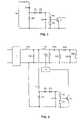
- FIG. 1shows an outline circuit diagram of the detection circuit presented in the invention.
- FIG. 2shows an outline circuit diagram of a ballast according to the invention.
- the input voltage Ue of a SEPIC converter(not illustrated in FIG. 1 ) is applied to a capacitive divider circuit formed from two capacitors C 1 and C 2 .
- the upper terminal of a resistive voltage divider circuit comprising two resistors R 1 and R 2is connected to the center tap of the divider circuit comprising the capacitors C 1 and C 2 , the lower terminals of the two divider circuits being connected to a common reference potential (internal ground).
- the center tap of the resistive voltage divider circuitcomprising the resistors R 1 and R 2 drives the base of a bipolar output transistor T 1 , whose collector terminal, in the emitter circuit, indirectly drives the base or the gate of a switching transistor (not shown) of the SEPIC converter, as is shown below in FIG. 2 .
- Incoming transient voltage peaksare introduced as an AC voltage by the capacitor C 1 , a rectifier diode D 2 , which is connected between the center tap of the capacitive divider circuit comprising the capacitors C 1 and C 2 and the internal reference potential, making it possible for the capacitor C 1 to subsequently be discharged.
- the detection circuit showndetects the input voltage Ue following rectification upstream of the SEPIC converter, with the result that account need only be taken of the polarity of the transient disturbances.
- the transient disturbances which are introduced as an AC voltageare passed on via a Zener diode D 3 to the resistive voltage divider circuit, and thus only get beyond the Zener diode D 3 when they exceed the voltage threshold specified by it.
- the resistive voltage divider circuitcomprising the resistors R 1 and R 2 then sets a suitable operating point by dividing the voltage signals to be expected into suitable values for driving the base of the output transistor T 1 .
- the capacitor C 2which has already been mentioned in the context of the capacitive divider circuit also forms, together with the resistors, essentially with the resistor R 1 , a timing element. That is to say, if the capacitor C 2 is charged by voltage pulses passing through the Zener diode D 3 , it is discharged via R 1 and the output transistor T 1 at a specific time constant. This time constant essentially defines a minimum time for which the output transistor T 1 is driven.
- the rectifier diode D 1 between the capacitors C 1 and C 2in this case prevents the capacitor C 2 from being discharged in an undesired manner.
- FIG. 2shows the detection circuit from FIG. 1 in an electronic ballast according to the invention.
- an AC supply voltagegenerally a conventional household system voltage
- a bridge rectifier BIn FIG. 2 , there is thus a rectified, positive potential on the upper horizontal conductive branch, and a rectified, negative potential, which is generally the reference potential, on the lower conductive branch which is parallel thereto.
- the rectified AC voltageforms the input of a SEPIC converter, which has the inductors L 20 and L 21 , the capacitor C 20 , the rectifier diode D 20 and the switching transistor S 20 and is driven by a drive circuit A.
- a further inductor L 10 and a further capacitor C 10which are used for filtering purposes, are connected between the bridge rectifier and the SEPIC converter.
- a load R 31Connected to the output (shown on the right) of the SEPIC converter, i.e. in parallel with a storage capacitor C 30 , is a load R 31 , which is supplied with a DC voltage made available by the capacitor C 30 .
- the load R 31is a conventional half-bridge oscillator having two switching transistors for producing a high-frequency AC voltage, with which a low-pressure gas discharge lamp can be operated. Since such circuits constitute prior art and are generally known, the load is merely represented by a resistor in this case.
- the capacitor C 30acts as a storage capacitor and must be charged by the SEPIC converter from the rectified AC voltage to a DC voltage which is as constant as possible.
- the power consumption from the power supply systemshould be matched to the sinusoidal waveform of the system voltage with as few disturbances as possible.
- the coil L 20is charged from the rectified system voltage to a specific current and, when the switching transistor S 20 is open, said coil L 20 is discharged to the capacitor C 20 .
- the coil L 21is charged when the switching transistor S 20 is closed and is discharged to the storage capacitor C 20 when the switching transistor S 20 is open.
- the polarity of the diode D 20is to be taken into consideration. So-called intermittent operation results when the times for which the switching transistor S 20 is open are sufficiently long for the current in the rectifier diode D 20 to be reduced to zero. In this case, on average, the capacitor C 20 is essentially charged to the value of the supply voltage rectified at that time.
- a corresponding clock ratioi.e. the ratio between the times for which the switching transistor is closed and open, thus makes it possible, taking into account the load R 31 , to set essentially any desired DC voltage across the capacitor C 30 which may, in particular, be smaller than the amplitude of the system voltage.
- the SEPIC converterthen functions as a step-down converter.
- the capacitor C 20to a certain extent decouples the two inductors L 20 and L 21 from one another, such that, in contrast to simple step-up converters, the voltages produced by the coil L 20 do not add up to the instantaneous system voltage.
- the intermittent switching operation of the switching transistor S 20is ensured by the drive circuit A, which is provided in the form a microcontroller and which can be inactivated in turn via the output transistor T 1 already mentioned.
- the output transistor T 1fundamentally quantizes between two states in response to the voltage tap at the resistive voltage divider circuit comprising the resistors R 1 and R 2 .
- the output signal of the output transistor T 1is fed to an AND gate in the drive circuit A, which may result in the drive for the switching transistor S 20 being disabled as described.
- the voltage referenced Ue in FIG. 1is tapped off in the manner shown in FIG. 2 at the filtered output of the bridge rectifier, but could also be tapped off directly at the output, i.e. upstream of the filter. These two possibilities must be weighed up in the individual case depending on whether filtering is helpful for the detection or not.
- the switching transistor S 20 of the SEPIC convertercan be reliably disconnected within a few microseconds. This prevents, in particular, transient overvoltages resulting in currents which are too high and which could represent a risk for the switching transistor S 20 when the switching transistor S 20 is connected in this phase, owing to saturation of the storage inductor L 20 of the SEPIC converter.
- voltage levelsmay be exceeded, which would exacerbate the problem described, following transient disturbances, as a result of LC resonance in the converter, but also in the system filter.
- the protective function of the inventionmay also relate to voltages in this case.
- the input and the output voltageare added, but without clocking only the input voltage is still applied to the switching transistor.
- the switching transistorcan thus be at risk in terms of voltage here too, and is protected by being disconnected.
- the inventionthus overall offers a simple, favorable and effective way of protecting the converter and thus the entire ballast from transient disturbances.
- itmay easily be combined with other protective measures, for example those which respond to the voltage values per se (i.e. the amplitude).
Landscapes
- Engineering & Computer Science (AREA)
- Power Engineering (AREA)
- Dc-Dc Converters (AREA)
- Circuit Arrangements For Discharge Lamps (AREA)
Abstract
Description
Claims (15)
Applications Claiming Priority (2)
| Application Number | Priority Date | Filing Date | Title |
|---|---|---|---|
| DE10349036ADE10349036A1 (en) | 2003-10-22 | 2003-10-22 | Electronic ballast with protection circuit for the switching transistor of a converter |
| DE10349036.1 | 2003-10-22 |
Publications (2)
| Publication Number | Publication Date |
|---|---|
| US20050088109A1 US20050088109A1 (en) | 2005-04-28 |
| US7196479B2true US7196479B2 (en) | 2007-03-27 |
Family
ID=34384396
Family Applications (1)
| Application Number | Title | Priority Date | Filing Date |
|---|---|---|---|
| US10/963,533Expired - Fee RelatedUS7196479B2 (en) | 2003-10-22 | 2004-10-14 | Electronic ballast having a protective circuit for a switching transistor of a converter |
Country Status (7)
| Country | Link |
|---|---|
| US (1) | US7196479B2 (en) |
| EP (1) | EP1526622B1 (en) |
| KR (1) | KR101052638B1 (en) |
| CN (1) | CN1610475A (en) |
| CA (1) | CA2485384A1 (en) |
| DE (1) | DE10349036A1 (en) |
| TW (1) | TW200518414A (en) |
Cited By (7)
| Publication number | Priority date | Publication date | Assignee | Title |
|---|---|---|---|---|
| US20060192541A1 (en)* | 2003-08-27 | 2006-08-31 | Michael Hackner | Switching regulator |
| US20060226817A1 (en)* | 2005-04-07 | 2006-10-12 | Patent-Treuhand-Gesellschaft Fur Elektrisch Gluhlampen Mbh | Metal halide lamp |
| US20070018592A1 (en)* | 2005-07-07 | 2007-01-25 | Olaf Busse | Circuit arrangement and method for operating at least one electric lamp |
| US20090034140A1 (en)* | 2006-02-13 | 2009-02-05 | Osram Gesellschaft mit beschränkter Haftung | Circuit Arrangement for Providing a DC Operating Voltage |
| US20100308740A1 (en)* | 2009-06-04 | 2010-12-09 | Osram Gesellschaft Mit Beschraenkter Haftung | Electronic ballast and method for operating at least one discharge lamp |
| US8471475B1 (en)* | 2010-07-23 | 2013-06-25 | Universal Lighting Technologies, Inc. | Modular dimming ballast with decoupled half-bridge topology |
| US9125281B2 (en) | 2009-08-10 | 2015-09-01 | Osram Gesellschaft Mit Beschrankter Haftung | Method for controlling a voltage transformer for overvoltage protection, voltage transformer and operating device having a voltage transformer |
Families Citing this family (8)
| Publication number | Priority date | Publication date | Assignee | Title |
|---|---|---|---|---|
| KR100891115B1 (en) | 2007-04-26 | 2009-03-30 | 삼성전자주식회사 | Method and apparatus for improving power factor that prevents saturation |
| DE102009035371B4 (en) | 2009-07-30 | 2017-10-26 | Osram Gmbh | Electronic ballast for operating at least one discharge lamp |
| US8140041B2 (en)* | 2009-08-27 | 2012-03-20 | Mediatek Inc. | Tunable capacitive device with linearization technique employed therein |
| DE102012011755A1 (en) | 2012-06-12 | 2013-12-12 | Tridonic Gmbh & Co. Kg | Power factor correction circuit, lighting device and method of controlling a power factor correction circuit |
| ES2535245B1 (en) | 2013-11-05 | 2016-02-16 | Bsh Electrodomésticos España, S.A. | Induction cooking field device |
| DE102014210003A1 (en) | 2014-05-26 | 2015-11-26 | Robert Bosch Gmbh | Heating device with filtration function |
| DE102014210797A1 (en) | 2014-06-05 | 2015-12-17 | Osram Gmbh | Circuit arrangement for converting voltages |
| JP2020190491A (en)* | 2019-05-22 | 2020-11-26 | 株式会社東芝 | Peak hold circuit and power converter |
Citations (10)
| Publication number | Priority date | Publication date | Assignee | Title |
|---|---|---|---|---|
| US3702434A (en)* | 1970-12-18 | 1972-11-07 | Owens Illinois Inc | Power supply system and control circuits therefor |
| US3946280A (en)* | 1975-03-10 | 1976-03-23 | Branson Ultrasonics Corporation | Overload protection circuit |
| US4020408A (en)* | 1975-10-02 | 1977-04-26 | Etatech, Inc. | Pulse width modulated DC-to-DC power converter using a single ended transformer |
| US4884180A (en)* | 1987-12-08 | 1989-11-28 | Wandel & Goltermann Gmbh & Co. | Regulated direct-current converter |
| US5430405A (en)* | 1992-08-12 | 1995-07-04 | Lambda Electronics Inc. | Control circuit for converters operating in the discontinuous mode |
| US5677602A (en)* | 1995-05-26 | 1997-10-14 | Paul; Jon D. | High efficiency electronic ballast for high intensity discharge lamps |
| US6181079B1 (en)* | 1999-12-20 | 2001-01-30 | Philips Electronics North America Corporation | High power electronic ballast with an integrated magnetic component |
| DE10110239A1 (en) | 2001-01-24 | 2002-07-25 | Patent Treuhand Ges Fuer Elektrische Gluehlampen Mbh | Electronic operating device for lamps with SEPIC converters, has first stage designed as SEPIC converter with time discrete regulation with control intervals longer than half mains period |
| US20040041621A1 (en)* | 2002-09-04 | 2004-03-04 | Patent-Treuhand-Gesellschaft Fur Elektrisch Gluhlampen Mbh | Operating circuit with an improved power supply for a driver circuit |
| US20040051479A1 (en)* | 2002-06-27 | 2004-03-18 | Patent-Treuhand-Gesellschaft Fur Elektrisch Gluhlampen Mbh | Supply circuit, in particular for a discharge lamp |
Family Cites Families (5)
| Publication number | Priority date | Publication date | Assignee | Title |
|---|---|---|---|---|
| EP0010811A1 (en)* | 1978-10-28 | 1980-05-14 | Westinghouse Brake And Signal Company Limited | Switching transistor over-voltage protection means |
| US4310866A (en)* | 1979-09-28 | 1982-01-12 | Borg-Warner Corporation | Shootthrough fault protection system for bipolar transistors in a voltage source transistor inverter |
| IT1225633B (en)* | 1988-11-30 | 1990-11-22 | Sgs Thomson Microelectronics | PROTECTION FROM NETWORK TRANSITORS. |
| DE10163034B4 (en)* | 2001-12-20 | 2014-08-28 | Tridonic Gmbh & Co Kg | Electronic ballast with overvoltage monitoring |
| US6678183B2 (en)* | 2002-03-20 | 2004-01-13 | Safco Corporation | DC power conditioning system |
- 2003
- 2003-10-22DEDE10349036Apatent/DE10349036A1/ennot_activeWithdrawn
- 2004
- 2004-09-16EPEP04022089Apatent/EP1526622B1/ennot_activeExpired - Lifetime
- 2004-09-20TWTW093128373Apatent/TW200518414A/enunknown
- 2004-10-14USUS10/963,533patent/US7196479B2/ennot_activeExpired - Fee Related
- 2004-10-20CACA002485384Apatent/CA2485384A1/ennot_activeAbandoned
- 2004-10-21KRKR1020040084271Apatent/KR101052638B1/ennot_activeExpired - Fee Related
- 2004-10-22CNCNA2004100870400Apatent/CN1610475A/enactivePending
Patent Citations (11)
| Publication number | Priority date | Publication date | Assignee | Title |
|---|---|---|---|---|
| US3702434A (en)* | 1970-12-18 | 1972-11-07 | Owens Illinois Inc | Power supply system and control circuits therefor |
| US3946280A (en)* | 1975-03-10 | 1976-03-23 | Branson Ultrasonics Corporation | Overload protection circuit |
| US4020408A (en)* | 1975-10-02 | 1977-04-26 | Etatech, Inc. | Pulse width modulated DC-to-DC power converter using a single ended transformer |
| US4884180A (en)* | 1987-12-08 | 1989-11-28 | Wandel & Goltermann Gmbh & Co. | Regulated direct-current converter |
| US5430405A (en)* | 1992-08-12 | 1995-07-04 | Lambda Electronics Inc. | Control circuit for converters operating in the discontinuous mode |
| US5677602A (en)* | 1995-05-26 | 1997-10-14 | Paul; Jon D. | High efficiency electronic ballast for high intensity discharge lamps |
| US6181079B1 (en)* | 1999-12-20 | 2001-01-30 | Philips Electronics North America Corporation | High power electronic ballast with an integrated magnetic component |
| DE10110239A1 (en) | 2001-01-24 | 2002-07-25 | Patent Treuhand Ges Fuer Elektrische Gluehlampen Mbh | Electronic operating device for lamps with SEPIC converters, has first stage designed as SEPIC converter with time discrete regulation with control intervals longer than half mains period |
| US6690122B2 (en) | 2001-01-24 | 2004-02-10 | Patent Treuhand Gesellschaft Fur Elektrische Gluhlampen Mbh | Lamp ballast with SEPIC converter |
| US20040051479A1 (en)* | 2002-06-27 | 2004-03-18 | Patent-Treuhand-Gesellschaft Fur Elektrisch Gluhlampen Mbh | Supply circuit, in particular for a discharge lamp |
| US20040041621A1 (en)* | 2002-09-04 | 2004-03-04 | Patent-Treuhand-Gesellschaft Fur Elektrisch Gluhlampen Mbh | Operating circuit with an improved power supply for a driver circuit |
Cited By (12)
| Publication number | Priority date | Publication date | Assignee | Title |
|---|---|---|---|---|
| US20060192541A1 (en)* | 2003-08-27 | 2006-08-31 | Michael Hackner | Switching regulator |
| US7443145B2 (en)* | 2003-08-27 | 2008-10-28 | Fraunhofer-Gesellschaft Zur Foerderung Der Angewandten Forschung E.V. | Switching regulator |
| US20060226817A1 (en)* | 2005-04-07 | 2006-10-12 | Patent-Treuhand-Gesellschaft Fur Elektrisch Gluhlampen Mbh | Metal halide lamp |
| US7307387B2 (en)* | 2005-04-07 | 2007-12-11 | Patent-Treuhand-Gesellschaft für elektrische Glühlampen mbH | Switchable voltage converter |
| US20070018592A1 (en)* | 2005-07-07 | 2007-01-25 | Olaf Busse | Circuit arrangement and method for operating at least one electric lamp |
| US7327094B2 (en)* | 2005-07-07 | 2008-02-05 | Patent-Treuhand-Gesellschaft Fur Elektrische Gluhlampen Mbh | Circuit arrangement and method for operating at least one electric lamp |
| US20090034140A1 (en)* | 2006-02-13 | 2009-02-05 | Osram Gesellschaft mit beschränkter Haftung | Circuit Arrangement for Providing a DC Operating Voltage |
| US8085519B2 (en) | 2006-02-13 | 2011-12-27 | Osram Ag | Circuit arrangement for providing a DC operating voltage |
| US20100308740A1 (en)* | 2009-06-04 | 2010-12-09 | Osram Gesellschaft Mit Beschraenkter Haftung | Electronic ballast and method for operating at least one discharge lamp |
| US8410721B2 (en) | 2009-06-04 | 2013-04-02 | Osram Gesellschaft Mit Beschraenkter Haftung | Electronic ballast and method for operating at least one discharge lamp |
| US9125281B2 (en) | 2009-08-10 | 2015-09-01 | Osram Gesellschaft Mit Beschrankter Haftung | Method for controlling a voltage transformer for overvoltage protection, voltage transformer and operating device having a voltage transformer |
| US8471475B1 (en)* | 2010-07-23 | 2013-06-25 | Universal Lighting Technologies, Inc. | Modular dimming ballast with decoupled half-bridge topology |
Also Published As
| Publication number | Publication date |
|---|---|
| CA2485384A1 (en) | 2005-04-22 |
| TW200518414A (en) | 2005-06-01 |
| DE10349036A1 (en) | 2005-05-25 |
| KR101052638B1 (en) | 2011-07-28 |
| EP1526622A3 (en) | 2008-04-02 |
| EP1526622A2 (en) | 2005-04-27 |
| US20050088109A1 (en) | 2005-04-28 |
| KR20050039600A (en) | 2005-04-29 |
| EP1526622B1 (en) | 2012-04-11 |
| CN1610475A (en) | 2005-04-27 |
Similar Documents
| Publication | Publication Date | Title |
|---|---|---|
| US7196479B2 (en) | Electronic ballast having a protective circuit for a switching transistor of a converter | |
| US8085160B2 (en) | Load detector for a dimmer | |
| US5930130A (en) | Inrush protection circuit | |
| US7529107B2 (en) | Power supply and electronic ballast with voltage clamping circuit | |
| US20060220595A1 (en) | High frequency power source control circuit and protective circuit apparatus | |
| US8378590B2 (en) | Method for detection of non-zero-voltage switching operation of a ballast of fluorescent lamps, and ballast | |
| US20040145930A1 (en) | Power supply circuit | |
| US20070069658A1 (en) | Basic halogen convertor ic | |
| EP1740023A2 (en) | Ballast with output ground-fault protection | |
| US20020140370A1 (en) | Driving a hid lamp | |
| JP5975774B2 (en) | LED lighting device | |
| EP1742518A2 (en) | Method for protecting a ballast from an output ground-fault condition | |
| TW396714B (en) | Stabilizer IC with stop function | |
| US8482213B1 (en) | Electronic ballast with pulse detection circuit for lamp end of life and output short protection | |
| US7183721B2 (en) | Ballast with circuit for detecting and eliminating an arc condition | |
| US8134301B2 (en) | Step-up driver with minimal switching frequency | |
| US20040227471A1 (en) | Hybrid ballast control circuit in a simplified package | |
| US7045973B2 (en) | Operating circuit for a dielectrically impeded discharge lamp having an overvoltage protection circuit | |
| US8450934B2 (en) | Circuit arrangement and method for operating a low-pressure discharge lamp | |
| US7154230B2 (en) | Circuit arrangement for dimming at least one lamp | |
| JPH09237685A (en) | Lighting system | |
| US7888879B2 (en) | Circuit arrangement and method for operating at least one electric lamp | |
| GB2310328A (en) | Circuit arrangement for current limitation and for overvoltage protection | |
| HK1130369B (en) | Load detector for a dimmer | |
| KR19990047900A (en) | Electronic ballast |
Legal Events
| Date | Code | Title | Description |
|---|---|---|---|
| AS | Assignment | Owner name:PATENT-TREUHAND-GESELLSCHAFT FUR ELEKTRISCH GLUHLA Free format text:ASSIGNMENT OF ASSIGNORS INTEREST;ASSIGNOR:STORM, ARWED;REEL/FRAME:015893/0248 Effective date:20040428 | |
| STCF | Information on status: patent grant | Free format text:PATENTED CASE | |
| FEPP | Fee payment procedure | Free format text:PAYOR NUMBER ASSIGNED (ORIGINAL EVENT CODE: ASPN); ENTITY STATUS OF PATENT OWNER: LARGE ENTITY | |
| FPAY | Fee payment | Year of fee payment:4 | |
| FEPP | Fee payment procedure | Free format text:PAYOR NUMBER ASSIGNED (ORIGINAL EVENT CODE: ASPN); ENTITY STATUS OF PATENT OWNER: LARGE ENTITY Free format text:PAYER NUMBER DE-ASSIGNED (ORIGINAL EVENT CODE: RMPN); ENTITY STATUS OF PATENT OWNER: LARGE ENTITY | |
| FPAY | Fee payment | Year of fee payment:8 | |
| FEPP | Fee payment procedure | Free format text:MAINTENANCE FEE REMINDER MAILED (ORIGINAL EVENT CODE: REM.); ENTITY STATUS OF PATENT OWNER: LARGE ENTITY | |
| LAPS | Lapse for failure to pay maintenance fees | Free format text:PATENT EXPIRED FOR FAILURE TO PAY MAINTENANCE FEES (ORIGINAL EVENT CODE: EXP.); ENTITY STATUS OF PATENT OWNER: LARGE ENTITY | |
| STCH | Information on status: patent discontinuation | Free format text:PATENT EXPIRED DUE TO NONPAYMENT OF MAINTENANCE FEES UNDER 37 CFR 1.362 | |
| FP | Lapsed due to failure to pay maintenance fee | Effective date:20190327 |