US7196354B1 - Wavelength-converting light-emitting devices - Google Patents
Wavelength-converting light-emitting devicesDownload PDFInfo
- Publication number
- US7196354B1 US7196354B1US11/238,667US23866705AUS7196354B1US 7196354 B1US7196354 B1US 7196354B1US 23866705 AUS23866705 AUS 23866705AUS 7196354 B1US7196354 B1US 7196354B1
- Authority
- US
- United States
- Prior art keywords
- light
- region
- wavelength
- converting
- thermally conductive
- Prior art date
- Legal status (The legal status is an assumption and is not a legal conclusion. Google has not performed a legal analysis and makes no representation as to the accuracy of the status listed.)
- Active, expires
Links
Images


Classifications
- H—ELECTRICITY
- H10—SEMICONDUCTOR DEVICES; ELECTRIC SOLID-STATE DEVICES NOT OTHERWISE PROVIDED FOR
- H10H—INORGANIC LIGHT-EMITTING SEMICONDUCTOR DEVICES HAVING POTENTIAL BARRIERS
- H10H20/00—Individual inorganic light-emitting semiconductor devices having potential barriers, e.g. light-emitting diodes [LED]
- H10H20/80—Constructional details
- H10H20/85—Packages
- H10H20/851—Wavelength conversion means
- H10H20/8515—Wavelength conversion means not being in contact with the bodies
- H—ELECTRICITY
- H10—SEMICONDUCTOR DEVICES; ELECTRIC SOLID-STATE DEVICES NOT OTHERWISE PROVIDED FOR
- H10H—INORGANIC LIGHT-EMITTING SEMICONDUCTOR DEVICES HAVING POTENTIAL BARRIERS
- H10H20/00—Individual inorganic light-emitting semiconductor devices having potential barriers, e.g. light-emitting diodes [LED]
- H10H20/80—Constructional details
- H10H20/85—Packages
- H10H20/858—Means for heat extraction or cooling
- H10H20/8583—Means for heat extraction or cooling not being in contact with the bodies
- H—ELECTRICITY
- H01—ELECTRIC ELEMENTS
- H01L—SEMICONDUCTOR DEVICES NOT COVERED BY CLASS H10
- H01L25/00—Assemblies consisting of a plurality of semiconductor or other solid state devices
- H01L25/03—Assemblies consisting of a plurality of semiconductor or other solid state devices all the devices being of a type provided for in a single subclass of subclasses H10B, H10D, H10F, H10H, H10K or H10N, e.g. assemblies of rectifier diodes
- H01L25/04—Assemblies consisting of a plurality of semiconductor or other solid state devices all the devices being of a type provided for in a single subclass of subclasses H10B, H10D, H10F, H10H, H10K or H10N, e.g. assemblies of rectifier diodes the devices not having separate containers
- H01L25/075—Assemblies consisting of a plurality of semiconductor or other solid state devices all the devices being of a type provided for in a single subclass of subclasses H10B, H10D, H10F, H10H, H10K or H10N, e.g. assemblies of rectifier diodes the devices not having separate containers the devices being of a type provided for in group H10H20/00
- H01L25/0753—Assemblies consisting of a plurality of semiconductor or other solid state devices all the devices being of a type provided for in a single subclass of subclasses H10B, H10D, H10F, H10H, H10K or H10N, e.g. assemblies of rectifier diodes the devices not having separate containers the devices being of a type provided for in group H10H20/00 the devices being arranged next to each other
- H—ELECTRICITY
- H01—ELECTRIC ELEMENTS
- H01L—SEMICONDUCTOR DEVICES NOT COVERED BY CLASS H10
- H01L2924/00—Indexing scheme for arrangements or methods for connecting or disconnecting semiconductor or solid-state bodies as covered by H01L24/00
- H01L2924/0001—Technical content checked by a classifier
- H01L2924/0002—Not covered by any one of groups H01L24/00, H01L24/00 and H01L2224/00
- H—ELECTRICITY
- H10—SEMICONDUCTOR DEVICES; ELECTRIC SOLID-STATE DEVICES NOT OTHERWISE PROVIDED FOR
- H10H—INORGANIC LIGHT-EMITTING SEMICONDUCTOR DEVICES HAVING POTENTIAL BARRIERS
- H10H20/00—Individual inorganic light-emitting semiconductor devices having potential barriers, e.g. light-emitting diodes [LED]
- H10H20/80—Constructional details
- H10H20/85—Packages
- H10H20/858—Means for heat extraction or cooling
- H10H20/8586—Means for heat extraction or cooling comprising fluids, e.g. heat-pipes
Definitions
- the inventionrelates generally to light-emitting devices, as well as related components, systems and methods, and, more particularly to light-emitting diodes (LEDs) and associated wavelength-converting regions.
- LEDslight-emitting diodes
- Light-emitting devicesmay include a wavelength-converting region (e.g., phosphor region) which can absorb light from a light-generating region (e.g., semiconductor region within an LED) and emit light having a different wavelength.
- a light-emitting device incorporating a wavelength-converting regioncan emit light having wavelength(s) that may not be possible using an LED without such regions.
- a GaN-based LEDmay emit blue light which can be converted to yellow light by a (Y,Gd)(Al,Ga)G:Ce 3+ or “YAG” (yttrium, aluminum, garnet) phosphor. Any unconverted blue light can be filtered so that the light-emitting device can emit only yellow light.
- the combined emission from a GaN-based LED and a YAG phosphormay generate white light as a result of combining blue light emitted from the LED and yellow light generated by the phosphor due to the conversion of some of the blue light.
- the inventionprovides light-emitting devices, as well as related components, systems and methods.
- a light-emitting devicecomprising a light-generating region adapted to generate light, a wavelength-converting region, and a thermally conductive region.
- the wavelength-converting regionis capable of absorbing light generated by the light-generating region and emitting light having a different wavelength than a wavelength of the light generated by the light-generating region.
- the thermally conductive regionis in contact with the wavelength-converting region and is capable of conducting heat generated in the wavelength-converting region.
- the thermally conductive regioncomprises a material having a thermal conductivity greater than a thermal conductivity of the wavelength-converting region.
- the light-emitting deviceis adapted to emit light having a total power of greater than 0.5 Watts.
- a light-emitting devicecomprising a light-generating region adapted to generate light, a wavelength-converting region, and a thermally conductive region.
- the wavelength-converting regionis capable of absorbing light generated by the light-generating region having a total power of greater than 0.5 Watts and emitting light having a different wavelength than a wavelength of the light generated by the light-generating region.
- the thermally conductive regionis in contact with the wavelength-converting region and is capable of conducting heat generated in the wavelength-converting region.
- the thermally conductive regioncomprises a material having a thermal conductivity greater than a thermal conductivity of the wavelength-converting region.
- a method of operating a light-emitting deviceincludes generating light in a light-generating region of an LED having a total power of greater than 0.5 Watts. The method further includes absorbing light generated by the light-generating region in a wavelength-converting region and emitting light having a wavelength different than a wavelength of the light generated in the light-generating region. The method further includes emitting light from the light-emitting device.
- the devicehas an operating lifetime of greater than 2,000 hours.
- a method of forming a light-emitting devicecomprises forming a light-generating region adapted to generate light, and forming a wavelength-converting region capable of absorbing light generated by the light-generating region and emitting light having a different wavelength than a wavelength of the light generated by the light-generating region.
- the methodfurther comprises forming a thermally conductive region in contact with the wavelength-converting region and capable of conducting heat generated in the wavelength-converting region, wherein the thermally conductive region comprises a material having a thermal conductivity greater than a thermal conductivity of the wavelength-converting region.
- the light-emitting deviceis adapted to emit light having a total power of greater than 0.5 Watts.
- FIG. 1 ais schematic of a light-emitting device including a light-generating region, a wavelength-converting region and a thermally conductive region in accordance with one embodiment of the invention
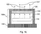
- FIG. 1 bis schematic of a light-emitting device including a light-generating region, a wavelength-converting region and a thermally conductive region, where the thermally conductive region is in thermal contact with a heat sink, in accordance with one embodiment of the invention
- FIG. 1 cis a schematic of a representative LED that may be used as a light-generating region in the devices of FIGS. 1 a and 1 b in accordance with one embodiment of the invention
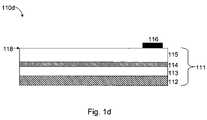
- FIG. 1 dis a schematic of another representative LED that may be used as a light-generating region in the devices of FIGS. 1 a and 1 b in accordance with one embodiment of the invention
- FIG. 1 eis a top view of a representative LED emitting surface having a dielectric function that varies spatially and which can be used in the LEDs of FIGS. 1 c and 1 d in accordance with one embodiment of the invention;
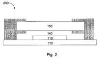
- FIG. 2is a schematic of a light-emitting device including a package window and frame in accordance with one embodiment of the invention
- FIGS. 3 a – 3 eare schematics of package windows suitable for use in light-emitting devices in accordance with some embodiments of the invention.
- FIGS. 4 a–bare schematics of light-emitting devices where a wavelength-converting region and a thermally conductive region are physically separated from a light-generating region in accordance with some embodiments of the invention
- FIG. 5is a schematic of a light-emitting device where a reflective surface is configured to reflect light generated by a light-generating region toward one or more wavelength-converting region(s) in accordance with one embodiment of the invention
- FIG. 6is a schematic of a light-emitting device where a light pipe can include a wavelength-converting region in accordance with one embodiment of the invention
- FIG. 7is a schematic of a light-emitting device where a wavelength-converting region is arranged alongside sidewalls of one or more light-generating regions in accordance with one embodiment of the invention
- FIGS. 8 a–care top views of the light-emitting device of FIG. 7 in accordance with some embodiments of the invention.
- FIG. 9is a schematic of a light-emitting device including a cavity in accordance with one embodiment of the invention.
- FIG. 10is a schematic of a multi-layer stack of an LED that includes a wavelength-converting region in accordance with one embodiment of the invention.
- FIG. 11is a schematic of a multi-layer stack of an LED including a wavelength-converting region incorporated into an electrically and/or thermally conductive layer in accordance with one embodiment of the invention.
- the light-emitting devicesmay include a thermally conductive region in contact with a wavelength-converting region (e.g., a phosphor region).
- the wavelength-converting regioncan absorb light emitted by a light-generating region (e.g., a semiconductor region) of the device and emit light having a different wavelength than that absorbed.
- the light-emitting devicescan emit light of wavelength(s) (and, thus, color) that may not be obtainable from devices that do not include wavelength-converting regions.
- the thermally conductive regionmay aid in the extraction of heat resulting from light absorption in the wavelength-converting region, which, if excessive, may impair device operation.
- thermally conductive regioncan enable devices including wavelength-converting regions to operate even at high power levels (e.g., light generated by the light-generating region and/or by the light-emitting device having a total power greater than about 0.5 Watts) for long operating lifetimes (e.g., greater than 2,000 hours).
- high power levelse.g., light generated by the light-generating region and/or by the light-emitting device having a total power greater than about 0.5 Watts
- long operating lifetimese.g., greater than 2,000 hours.
- FIG. 1 aillustrates a light-emitting device 100 a including a light-generating region 110 , a wavelength-converting region 120 , and a thermally conductive region 130 in contact with at least a portion of the wavelength-converting region 120 , in accordance with some embodiments.
- the light-generating regionmay be an LED that includes an active region (e.g., a quantum well structure).
- Region 110may be operated to generate light 101 that enters the wavelength-converting region 120 , where at least some of the light is converted to light 102 having one or more wavelengths different than the wavelength of generated light 101 .
- a portion of light 101may pass through the wavelength-converting region without being converted to light having a different wavelength (i.e., light 102 ).
- substantially all of the light being generated in region 110is converted in the wavelength-converting region.
- the emission of light from the light-emitting deviceincludes the combination of light 101 ′ and light 102 . For example, if light 101 ′ has a wavelength characteristic of blue light and light 102 has a wavelength characteristic of yellow light, then the combined emission (i.e., light 101 ′ and 102 ) may appear white.
- FIG. 1 billustrates a light-emitting device 100 b similar to the light-emitting device 100 a , but having a thermally conductive region 130 in thermal contact with a heat sink 135 that may be external to device 100 b.
- FIGS. 1 a and 1 bneed be present in all embodiments of the invention and that the illustrated features may be otherwise positioned within the light-emitting device. Also, additional features may be present in other embodiments. Additional embodiments are shown in the other figures and/or described further below.
- a featuree.g., layer, region, substrate, heat sink
- a featurecan be directly on the feature, or an intervening feature (e.g., layer) also may be present.
- a feature that is “directly on” or “in contact with” another featuremeans that no intervening feature is present. It should also be understood that when a feature is referred to as being “on”, “over”, “overlying”, or “in contact with” another feature, it may cover the entire feature or a portion of the feature.
- a feature that is “adjacent” to another featuremay be directly on, directly under, or directly next to another feature.
- the light-generating regionmay be an LED or a portion of an LED.
- the light-generating region 110may be an active region (e.g., semiconductor region) of an LED, though it should be understood that the invention is not so limited.
- the light-generating regionis an active region an LED, it should be understood that the LED may be any suitable diode that emits light.
- LEDsinclude an active region comprising one or more semiconductors materials, including III–V semiconductors (e.g., gallium arsenide, aluminum gallium arsenide, gallium aluminum phosphide, gallium phosphide, gallium arsenide phosphide, indium gallium arsenide, indium arsenide, indium phosphide, gallium nitride, indium gallium nitride, indium gallium aluminum phosphide, aluminum gallium nitride, as well as combinations and alloys thereof), II–VI semiconductors (e.g., zinc selenide, cadmium selenide, zinc cadmium selenide, zinc telluride, zinc telluride selenide, zinc sulfide, zinc sulfide selenide, as well as combinations and alloys thereof), and/or other semiconductors.
- III–V semiconductorse.g., gallium arsenide, aluminum gallium arsenide, gallium aluminum pho
- the light-generating regionmay be other types of light-emitting devices including lasers, or portions thereof. It should also be understood that the light-generating region may be an array including more than one LED or portions thereof.
- FIG. 1 cillustrates a representative LED 110 c .
- the LEDcomprises a multi-layer stack 111 that may be disposed on a sub-mount (not shown).
- the multi-layer stack 111can include an active region 114 which is formed between n-doped layer(s) 115 and p-doped layer(s) 113 .
- the stackalso includes a conductive layer 112 .
- An n-side contact pad 116is disposed on layer 115
- a p-side contact pad 117is disposed on conductive layer 112 . It should be appreciated that the LED is not limited to the configuration shown in FIG.
- the n-doped and p-doped sidesmay be interchanged so as to form an LED having a p-doped region in contact with the contact pad 116 and an n-doped region in contact with the contact pad 117 .
- electrical potentialmay be applied to the contact pads which can result in light generation within active region 114 and emission of at least some of the light generated through an emitting surface 118 .
- FIG. 1 dillustrates another representative LED 110 d .
- the LED 110 dis similar in many respects to LED 110 c , except that electrode 117 is absent. Instead, electrical contact to the layer(s) 113 is made via conductive layer 112 through a conductive submount (not shown) which is attached to conductive layer 112 . It should be understood that various other modifications can be made to the representative LED structures presented, and that the invention is not limited in this respect.
- the active region of an LEDincludes one or more quantum wells surrounded by barrier layers.
- the quantum well structuremay be defined by a semiconductor material layer (e.g., in a single quantum well), or more than one semiconductor material layers (e.g., in multiple quantum wells), with a smaller band gap as compared to the barrier layers.
- Suitable semiconductor material layers for the quantum well structuresinclude InGaN, AlGaN, GaN and combinations of these layers (e.g., alternating InGaN/GaN layers, where a GaN layer serves as a barrier layer).
- the n-doped layer(s) 115include a silicon-doped GaN layer (e.g., having a thickness of about 300 nm thick) and/or the p-doped layer(s) 113 include a magnesium-doped GaN layer (e.g., having a thickness of about 40 nm thick).
- the conductive layer 112may be a silver layer (e.g., having a thickness of about 100 nm), which may also serve as a reflective layer (e.g., that reflects upwards any downward propagating light generated by the active region 114 ).
- other layersmay also be included in the LED; for example, an AlGaN layer may be disposed between the active region 114 and the p-doped layer(s) 113 .
- compositions other than those described hereinmay also be suitable for the layers of the LED.
- emitting surface 118 of the LEDhas a dielectric function that varies spatially which can improve the extraction efficiency of light generated by the LED and may enable the high power levels described further below.
- the dielectric functioncan vary spatially according to a pattern.
- the patternmay be periodic (e.g., having a simple repeat cell, or having a complex repeat super-cell), periodic with de-tuning, or non-periodic.
- non-periodic patternsinclude quasi-crystal patterns, for example, quasi-crystal patterns having 8-fold symmetry.
- a non-periodic patterncan also include random surface roughness patterns having a root-mean-square (rms) roughness on the order of the wavelength of the generated light.
- the emitting surfaceis patterned with openings which can form a photonic lattice.
- Suitable LEDs having a dielectric function that varies spatiallyhave been described in, for example, U.S. Pat. No. 6,831,302 B2, entitled “Light Emitting Devices with Improved Extraction Efficiency,” filed on Nov. 26, 2003, which is herein incorporated by reference in its entirety.
- FIG. 1 eillustrates a representative LED emitting surface 118 ′ having a dielectric function that varies spatially.
- the spatial variation of the dielectric functionis a result of openings in the emitting surface 118 ′ of the LED.
- the emitting surface 118 ′is not flat, but rather consists of a modified triangular pattern of openings 119 ′.
- various valuescan be selected for the depth of openings 119 ′, the diameter of openings 119 ′ and/or the spacing between nearest neighbors in openings 1119 ′.
- the triangular pattern of openingsmay be detuned so that the nearest neighbors in the pattern have a center-to-center distance with a value between (a ⁇ a) and (a+ ⁇ a), where “a” is the lattice constant for an ideal triangular pattern and “ ⁇ a” is a detuning parameter with dimensions of length and where the detuning can occur in random directions.
- a detuning parameter, ⁇ ais generally at least about one percent (e.g., at least about two percent, at least about three percent, at least about four percent, at least about five percent) of ideal lattice constant, a, and/or at most about 25% (e.g., at most about 20%, at most about 15%, at most about 10%) of ideal lattice constant, a.
- the nearest neighbor spacingsvary substantially randomly between (a ⁇ a) and (a+ ⁇ a), such that pattern of openings is substantially randomly detuned.
- a non-zero detuning parameterenhances the extraction efficiency of the LED. It should be appreciated that numerous other modifications are possible to the emitting surface of an LED while still achieving a dielectric function that varies spatially.
- Lightmay be generated by LED 110 c (or 110 d ) as follows.
- the p-side contact pad 117(or conductive layer 112 ) can be held at a positive potential relative to the n-side contact pad 116 , which causes electrical current to be injected into the LED.
- electrons from n-doped layer(s) 115can combine in the active region with holes from p-doped layer(s) 113 , which can cause the active region to generate light.
- the active regioncan contain a multitude of point dipole radiation sources that emit light (e.g., isotropically) within the region with a spectrum of wavelengths characteristic of the material from which the active region is formed.
- the spectrum of wavelengths of light generated by the light-generating regioncan have a peak wavelength of about 445 nanometers (nm) and a full width at half maximum (FWHM) of about 30 nm, which is perceived by human eyes as blue light.
- the light-generating regioncan generate light having a peak wavelength corresponding to ultraviolet light (e.g., having a peak wavelength of about 370–390 nm), violet light (e.g., having a peak wavelength of about 390–430 nm), blue light (e.g., having a peak wavelength of about 430–480 nm), cyan light (e.g., having a peak wavelength of about 480–500 nm), green light (e.g., having a peak wavelength of about 500 to 550 nm), yellow-green (e.g., having a peak wavelength of about 550–575 nm), yellow light (e.g., having a peak wavelength of about 575–595 nm), amber light (e.g., having a peak wavelength of about 595–605 nm), orange light (e.g., having a peak wavelength of about 605–620 nm), red light (e.g., having a peak wavelength of about 620–700 .
- region 110it may be preferable in certain embodiments for region 110 to generate light having a high power.
- the light-generating regionis an LED
- the light emitted by the LEDcan have a high power.
- the light generated by region 110may have a total power greater than 0.5 Watts, greater than 1 Watt, greater than 5 Watts, or greater than 10 Watts. In some cases, the light generated has a total power of less than 100 Watts, though this should not be construed as a limitation of all embodiments of the invention.
- the desired powerdepends, in part, on the application.
- the total power of the generated lightcan be measured by using an integrating sphere equipped with spectrometer, for example a SLM12 from Sphere Optics Lab Systems
- the light generated by region 110may also have a high total power flux.
- total power fluxrefers to the total power divided by the emission area. In some embodiments, the total power flux is greater than 0.03 Watts/mm 2 , greater than 0.05 Watts/mm 2 , greater than 0.1 Watts/mm 2 , or greater than 0.2 Watts/mm 2 .
- Wavelength-converting region 120is a region that can include one or more wavelength-converting materials that can convert the wavelength of absorbed light.
- the wavelength-converting materialscan function by absorbing light having a first wavelength and emitting light having a second wavelength (e.g., longer wavelengths).
- the wavelength-converting regionincludes a phosphor material.
- the phosphor materialcan be present in particulate form.
- the particlesmay be distributed in a second material (e.g., an encapsulant or adhesive, such as epoxy) to form a composite structure.
- the phosphor materialmay be a yellow phosphor material (e.g., (Y,Gd)(Al,Ga)G:Ce 3+ , sometimes referred to as a “YAG” (yttrium, aluminum, garnet) phosphor), a red phosphor material (e.g., L 2 O 2 S:Eu 3+ ), a green phosphor material (e.g., ZnS:Cu,Al,Mn), and/or a blue phosphor material (e.g., (Sr,Ca,Ba,Mg) 10 (PO 4 ) 6 Cl:Eu 2+ ).
- YAGyttrium, aluminum, garnet
- red phosphor materiale.g., L 2 O 2 S:Eu 3+
- a green phosphor materiale.g., ZnS:Cu,Al,Mn
- a blue phosphor materiale.g., (Sr,Ca,Ba,Mg) 10
- the wavelength-converting regionmay include nanodots (also, referred to as “quantum dots” or “semiconductor nanocrystals”).
- the nanodotscan be distributed in a second material (e.g., an encapsulant or adhesive, such as epoxy, or an insulator, such as glass) to form a composite structure.
- a second materiale.g., an encapsulant or adhesive, such as epoxy, or an insulator, such as glass
- semiconductor nanodotscan be formed of group IV semiconductors (e.g., silicon, germanium), III–V semiconductors, II–VI semiconductors, and combinations thereof, as the invention is not limited so.
- Nanodotscan include a core region, formed of a suitable material, and one or more shell layers.
- Light emission wavelength(s) from the nanodotscan depend on the materials that form the nanodots and/or the diameter of the nanodots. These factors can influence the energy levels of carriers (e.g., electrons, holes) within the nanodots and hence determine absorption and/or emission wavelength(s).
- carrierse.g., electrons, holes
- nanodots having a CdSe core and a diameter of about 1.9 nm to about 6.7 nmmay emit light having wavelengths between about 465 nm to 640 nm; nanodots having a CdSe core, a ZnS shell, and a diameter of about 2.9 nm to about 6.1 nm may emit light having wavelengths between 490 nm to 620 nm; nanodots having a CdTe core, a CdS shell, and a diameter of about 3.7 nm to about 4.8 nm may emit light having wavelengths between 620 nm to 680 nm; nanodots having a PbS core and a diameter of about 2.3 nm to about 2.9 nm may emit light having wavelengths between 850 nm to 950 nm; nanodots having a PbSe core and a diameter of about 3.5 nm to about 9 nm may emit light having wavelengths
- the wavelength-converting regionmay be in the form of a coating on one or more surfaces within the light-emitting device 100 a or 100 b (e.g., the surface of a package window, the surface of an LED, etc.).
- the wavelength converting regionmay comprise multiple layers including different wavelength-converting materials, which can be disposed over each other.
- FIGS. 1 a and 1 bshow the wavelength-converting region as a layer disposed over the light-generating region and in contact with the thermally conductive region along a top surface, it should be appreciated that other configurations are possible. As described further below, the wavelength-converting region may be configured in any manner so as to facilitate the conversion of part or all of the light emitted by the light-generating region.
- the light generated by region 110may be converted to light of different wavelength(s) by the wavelength-converting region 120 .
- any part of the light from region 110 that is not converted by the wavelength-converting region 120can be filtered from the emission of the light-emitting device 100 a or 100 b (e.g., using a filter in the path of light emission 101 ′ and 102 ), thereby resulting in emitted light having only the wavelength(s) generated by the wavelength-converting region.
- the filtermay reflect non-converted light back through the wavelength-converting region so that it may be converted.
- a filtercan be disposed under the wavelength-converting region which can allow light from the LED to pass while reflecting light generated in the wavelength-converting region.
- a filterneed not necessarily be used to filter out wavelengths of light. As described below, this approach may be used to generate white light.
- an antireflective coatingcan be used to enhance emission out of the wavelength-converting region.
- the wavelength-converting regioncan emit yellow light, for example, a (Y,Gd)(Al,Ga)G:Ce 3+ phosphor.
- the wavelength-converting regioncan be activated and emit light (e.g., isotropically) with a broad spectrum centered around yellow wavelengths (e.g., about 575–595 nm).
- a viewer of the total light spectrum emerging from light-emitting device 100 a or 100 bsees the yellow broad emission spectrum from the wavelength-converting region and the blue narrow emission spectrum from the light-generating region (e.g., from the GaN LED) and typically mixes the two spectra to perceive white.
- light generated by the light-generating region 110can have a spectrum centered in the ultraviolet (or violet, or blue) wavelength range
- the wavelength-converting region 120can emit light having a plurality of wavelengths including red, green, and blue wavelengths.
- the wavelength-converting regioncan include a red phosphor material (e.g., L 2 O 2 S:Eu 3+ ), a green phosphor material (e.g., ZnS:Cu,Al,Mn), and a blue phosphor material (e.g., (Sr,Ca,Ba,Mg) 10 (PO 4 ) 6 Cl:Eu 2+ ).
- the wavelength-converting regioncan include nanodots that can emit light having a plurality of wavelengths including red, green, and blue wavelengths.
- a viewer of the total light spectrum emerging from the light-emitting devicesees the emission spectrum from the combined wavelength-converting region emission, including red, green, and blue emissions, and mixes these spectra to perceive white light.
- the wavelength-converting regionabsorbs light generated by region 110 having the high total power values (as well as, power flux and power density) noted above. It also may be preferable for the wavelength-converting region to emit light having the same high total power values.
- the wavelength-converting regionmay emit light having a total power greater than 0.5 Watts, greater than 1 Watt, greater than 5 Watts, or greater than 10 Watts. In some cases, the light emitted by the wavelength-converting region has a total power of less than 100 Watts, though this should not be construed as a limitation of all embodiments of the invention. The desired power depends, in part, on the application.
- the total power of light emitted from the wavelength-converting regionmay be equal to the total power of light emitted from the device.
- the wavelength-converting regionmay emit light having a lower power than the power of the light generated by the light generating region because of absorption within the wavelength-converting region.
- the wavelength-converting regionmay emit light having a power of about 50% (or between 50% and 100%) the power of light generated by the light-generating region.
- the light emitted by the wavelength-converting region (and device)still can have a high power.
- the power flux out of the wavelength-converting regionis dependent on the emission area of the wavelength-converting region.
- the power flux out of the wavelength-converting regioncan be less than the power flux out of the light-generating region since the wavelength-converting region can have an emission area that is larger than that of the light-generating region.
- the light-generating regionmay have an area of about 10 mm and the wavelength-generating region may have an emission area of about 100 mm 2 .
- the wavelength-converting regionmay emit light having a total power flux of greater than 3 mWatts/mm 2 , greater than 5 mWatts/mm 2 , greater than 10 mWatts/mm 2 , or greater than 20 mWatts/mm 2 .
- a total power density for the emission out of the wavelength-converting regioncan be determined by dividing the total power of light emitted out of the wavelength-converting region by the volume of the wavelength-converting region.
- the wavelength-converting regionmay have a volume of 100 mm 3 based on an emission area of 100 mm 2 and a thickness of 10 mm.
- the wavelength-converting regioncan have a total power density of greater than 0.5,m Watts/mm 3 , greater than 1 mWatts/mm 3 , greater than 5 mWatts/mm 3 , or greater than about 10 mWatts/mm 3 .
- Such high powerscan generate substantial amounts of heat in the wavelength-converting region which can impede the proper functioning of the light-emitting device.
- power levelscan lead to premature device failure, discoloring of the matrix material surrounding the wavelength-converting material (e.g., phosphor particles, nanodots), wavelength shift in the emission spectra, degradation in the conversion efficiency of the wavelength-converting material, and/or mechanical failure such as delamination.
- Thermally conductive region 130can aid in the extraction of heat from the wavelength-converting region which can enable operation at such high powers and/or high brightnesses of generated light.
- the thermally conductive region 130may comprise of one or more structures (which may include a void) that conduct heat away from the wavelength-converting region.
- the thermally conductive regionis typically in direct contact with the region so as to enable heat extraction and conduction away from the wavelength-converting region. In some embodiments, only a portion of the thermally conductive region is in contact with the wavelength-converting region. In other embodiments, substantially the entire area of the thermally conductive region is in contact with the wavelength-converting region. For example, the thermally conductive region may be surrounded by the wavelength-converting region.
- the thermally conductive regionmay include a single material layer, multiple material layers, or a portion of a layer.
- the thermally conductive region 130may include channels in which fluid (e.g., gas, such as air, and/or liquid, such as water) may flow there through so as to aid in heat extraction and/or conduction.
- fluide.g., gas, such as air, and/or liquid, such as water
- the thermally conductive regionmay be formed of one or more materials that have a thermal conductivity larger than that of the wavelength-converting region.
- the thermally conductive regionmay be formed of one or more metals (e.g., silver, copper, tungsten, molybdenum, aluminum, gold, platinum, palladium, etc.), metal oxides (e.g., indium tin oxide), ceramics (e.g., aluminum nitride ceramics), and/or other materials having a suitable thermal conductivity.
- the thermally conductive regionmay include carbon in the form of diamond or nanotubes.
- the thermally conductive regionmay comprise a composite of two or more different materials, such as copper tungsten, copper molybdenum, aluminum silicon, and/or aluminum silicon carbide.
- the thermally conductive regionmay be reflective to light emitted by the wavelength-converting region.
- the thermally conductive regionmay be formed of a suitable metal including those noted above.
- the thermally conductive regioncan serve as both a region than aids in the extraction of heat from the wavelength-converting region and a region that reflects light as desired for the operation of the light-emitting device.
- the thermally conductive regionis substantially transparent to light emitted by the phosphor region 120 and/or the light-emitting device 100 a or 100 b .
- the thermally conductive regionmay be formed of indium tin oxide, which may be substantially transparent (e.g., having a transmission coefficient greater than about 80%) for light having wavelengths greater than about 350 nm.
- the thermally conductive regioncan include a thin layer of metal (e.g., gold).
- the thermally conductive regioncould form part or all of any filters incorporated into a window of the light-emitting device.
- a transparent host substrate, on which a wavelength-converting region is depositedcan serve as a thermally conductive region (e.g., a sapphire or diamond substrate). The thermally conductive regions can conduct heat away from the wavelength-converting region to a heat sink (e.g., external and/or internal to the light-emitting device).
- the thermally conductive region 130may be contact with a top surface of the wavelength-converting region or in contact with a sidewall of the wavelength-converting region; the thermally conductive region may be embedded in the wavelength-converting region, and/or may be in contact with the wavelength-converting region in any other way, as the invention is not limited in this respect.
- the thermally conductive regionmay serve multiple purposes.
- the thermally conductive regionmay comprise all or a portion of a package frame of the light-emitting device.
- the thermally conductive regionitself, may also function as a heat sink.
- the thermal mass of the thermally conductive regionis sufficiently large to enable heat to be dissipated within the heat sink.
- the thermally conductive regionmay be connected to a heat sink. It should be understood that any of the other embodiments described herein may include a heat sink connected to the thermally conductive region.
- the heat sinkmay be combined with the light-emitting device 100 b in any suitable configuration so as to facilitate heat extraction from the thermally conductive region 130 .
- the heat sinkcan be connected to the backside of the light-emitting device 100 b , and the thermally conductive region 130 may include one or more surfaces exposed to the backside of the light-emitting device.
- a heat sinkmay be incorporated within the light-emitting device, as the invention is not limited so.
- the heat sinkmay be formed of one or more metals (e.g., silver, copper, tungsten, molybdenum, aluminum, gold, platinum, palladium, etc.), ceramics, and/or other materials having a suitable thermal conductivity and heat capacity.
- the heat sinkmay include aluminum nitride ceramics, and/or carbon.
- the heat sinkmay include a composite of two or more different materials, such as copper tungsten, copper molybdenum, aluminum silicon, and/or aluminum silicon carbide.
- the heat sinkcan include passive and/or active heat exchanging mechanisms, as the invention is not limited in this respect.
- Passive heat sinkscan include structures formed of one or more materials that conduct heat as a result of temperature differences in the structure. Passive heat sinks may also include protrusions (e.g., fins, combs, spikes, etc.) which can increase the surface contact area with the surrounding atmosphere and therefore increase the rate of heat exchange with the atmosphere.
- a passive heat sinkmay include a copper slug core, which provides a thermally conductive material that can conducts thermal energy to surrounding aluminum fins radiating out from the copper slug.
- a passive heat sinkmay also include channels in which fluid (e.g., liquid and/or gas) may flow there through so as to aid in heat extraction via convection within the fluid.
- Active heat sinksmay include one or more suitable means that can further aid in the extraction of heat.
- Such active heat sinkscan include mechanical, electrical, chemical and/or any other suitable means to facilitate the exchange of heat.
- an active heat sinkmay include a fan used to circulate air and therefore cool the heat sink.
- a pumpmay be used to circulate a fluid (e.g., liquid and/or gas) within channels in the heat sink.
- the heat sinkmay be connected to a thermal electric cooler that may further facilitate heat extraction from the heat sink.
- the heat sinkcan include the thermal electric cooler, or may consist solely of a thermal electric cooler.
- light-emitting devices of the inventionmay be any device that emits light, and is in no way limited by the illustrative light-emitting devices shown in FIGS. 1 a and 1 b .
- a light-emitting devicemay be a packaged LED comprising multiple elements (e.g., an LED (e.g., as shown in FIGS. 1 c and 1 d ), a wavelength-converting region, and a thermally conductive region).
- a light-emitting devicemay comprise any configuration of the elements, and is not limited to the configuration of the illustrative light-emitting devices 100 a and 100 b .
- the elements of the light-emitting deviceneed not be structurally connected.
- one or more of the elements of the light-emitting devicemay not be structurally connected to the other elements (e.g., the wavelength-converting region may not be structurally connected to the light-generating region).
- FIG. 2illustrates a light-emitting device 200 in accordance with some embodiments of the invention.
- the light-emitting device 200comprises a light-generating region 110 (e.g., an LED or several LEDs) that is disposed over a package substrate 170 , which can include electrically conductive portions, electrically isolating portions, and/or thermally conductive portions.
- Light generated by region 110can pass through a region 140 and a window 150 and may be subsequently emitted from device 200 .
- Region 140may comprise an encapsulant (e.g., epoxy), a gas (e.g., air, nitrogen) or a vacuum.
- a wavelength-converting regionmay be formed in the encapsulant (when region 140 includes an encapsulant) and/or the window.
- a window frame 160 of the packagecan function as a thermally conductive region which is in contact with at least a portion of the wavelength-converting region in the window and/or the encapsulant (when region 140 includes an encapsulant). Thus, heat generated within the wavelength-converting region may be conducted away from the region via the window frame.
- Frame 160in this embodiment, is made of a suitably thermally conductive material.
- the framemay also be in contact with the package substrate 170 , as shown.
- the framecan also include cooling channels enabling the flow of fluid (e.g., liquid and/or gas) that can be used to further aid in the extraction and conduction of heat.
- a pump mechanismcan be incorporated into the window frame to facilitate the flow of fluid through channels in the frame.
- the window frameserves as a thermally conductive region that can extract heat from the wavelength-converting region.
- the light-emitting device 200 and/or frame 160can be in thermal contact with an external heat sink (not shown).
- the wavelength-converting materialcan be applied to the window using various techniques, including thin layer deposition, spin-coating, and injection molding.
- wavelength-converting materialcan be added to a spin-on-glass solution and spun onto the window top and/or bottom surfaces, thereby forming one or more wavelength-converting layers.
- one or more wavelength-converting layerscan be sandwiched between two or more window layers.
- the wavelength-converting materialmay be incorporated homogeneously throughout the window or portions of the window.
- wavelength-converting materiale.g., phosphor particles, nanodots
- the windowcan comprise multiple layers and/or structures.
- the wavelength-converting materialcan be dispersed within the encapsulant material or can be layered over the encapsulant material.
- the windowmay also include a thermally conductive region.
- Heat conduction and/or dissipation mechanismscan be engineered into the window by the integration of thermally conductive materials and/or by increasing the surface area of the window.
- these thermally conductive regionsmay be thermally coupled.
- the thermally conductive region of the windowmay be able to facilitate the transport of heat out of the window and to the frame, thereby facilitating the cooling of the window.
- a LED and a phosphor containing windoware arranged such as FIG. 2 .
- the phosphor containing windowmay have a matching aspect ratio with respect to the emitting area of the LED.
- Such an aspect ratiocan be design to match the aspect ratio of a microdisplay (i.e. 16:9, 4:3) or of a desired collection optic, which are described in commonly-owned Luminus Patent Application Publication No. 2005-0127375, which is incorporated herein by reference and is based on U.S. patent application Ser. No. 10/872,335, filed Jun. 18, 2004.
- the length of at least one edge of the LEDis greater than 1 mm.
- the phosphor-containing windowis the same dimensions of the emitting area of the LED.
- FIGS. 3 a – 3 eillustrate different embodiments of package windows suitable for use in light-emitting devices of the present invention.
- FIG. 3 aillustrates an embodiment of a package window 150 a of a light-emitting device where the window comprises a thermally conductive layer.
- the windowincludes a substrate 151 (e.g., glass), a wavelength-converting region 120 , and a thermally conductive layer 155 a in thermal contact with the wavelength-converting region and serving as a thermally conductive region.
- the thermally conductive layermay also be in thermal contact with a window frame (e.g. frame 160 ) of a light-emitting device (e.g., light-emitting device 200 ).
- a window framee.g. frame 160
- a light-emitting devicee.g., light-emitting device 200
- multiple thermally conductive layerscan be sandwiched between wavelength-converting layers and/or multiple thermally conductive layers can be disposed upon each other.
- the thermally conductive layeris typically transparent to the desired emission wavelength of the light-emitting device and can comprise a suitable material having a thermal conductivity larger than the thermal conductivity of the wavelength-converting region.
- the thermally conductive layercan comprise a thin metal film (e.g., silver, gold, etc.), a metal oxide film (e.g., indium tin oxide), and/or a diamond coating.
- FIG. 3 billustrates an embodiment of a package window 150 b of a light-emitting device according to the invention.
- the windowincludes a patterned thermally conductive layer 155 b , on the wavelength-converting region 120 that serves as a thermally conductive region.
- the patterncan be a 1-dimensional or 2-dimensional grid that can extend along the window and which can be in thermal contact with a window frame (e.g. frame 160 ) of a light-emitting device (e.g., light-emitting device 200 ).
- FIG. 3 bshows the patterned layer on the surface of the wavelength-converting region 120 , it should be appreciated that the patterned layer can be embedded in the wavelength-converting layer, in the substrate, and/or at the interface between the wavelength-converting layer and the substrate.
- thermally conductive layer 155 bcan improve light transmission through the window as compared to windows where the thermally conductive layer is continuous. Such embodiments can facilitate the use of a thicker thermally conductive layer which can in turn result in increased heat transfer.
- FIG. 3 cillustrates an embodiment of a package window 150 c of a light-emitting device where a thermally conductive region is embedded within a wavelength-converting region.
- the thermally conductive regionmay include thermally conductive structures 155 c such as wires, fibers and/or tubes (e.g., carbon nanotubes).
- FIG. 3 cshows structures 155 c embedded within the wavelength-converting region, it should be appreciated that the structures may also be positioned on the wavelength-converting region and/or at the interface between the wavelength-converting region and the substrate.
- FIG. 3 dillustrates an embodiment of a package window 150 d of a light-emitting device where a thermally conductive region includes channels configured to have fluid (e.g., liquid and/or gas) flowing there through.
- Channels 156can be formed in the wavelength-converting layer (or the window substrate 151 ).
- Liquid (e.g., water) and/or gas (e.g., air)can flow through channels 156 providing heat exchange with the surrounding wavelength-converting region 120 , and thereby facilitating the cooling of the wavelength-converting region.
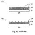
- FIG. 3 eillustrates an embodiment of a package window 150 e of a light-emitting device where an increased surface area on the package window increases heat extraction.
- Increasing the surface area of the windowcan provide increased cooling.
- Patterning one or more surfacesis one method of increasing the surface area and thereby increasing the heat extraction from the wavelength-converting region, as shown in FIG. 3 e .
- a patterned emission surface on the windowcan also increase light extraction out of the package window.
- the window substrate and/or wavelength-converting regioncan include thermally conductive particles (e.g., silver particles, gold particles, indium tin oxide particles, etc.).
- the window substratecould comprise a thermally conductive material layer that can be transparent to desired light emission wavelength(s) of the light-emitting device (e.g., diamond, sapphire, etc.).
- the windowscan include anti-reflection coating(s) (ARC) which can increase or maximize transmission of light, generated by a light-generating region, through the window.
- ARCanti-reflection coating
- the windowcan include an environmental protection layer that can protect the wavelength-converting region in the light-emitting device from moisture.
- the anti-reflection coatingsmay not be a part of the window and can otherwise be incorporated in the light-emitting device.
- the windowscan include one or more light filters.
- a filtercould be disposed beneath a wavelength-converting region which allows transmission of emitted light (e.g., UV, blue) from the light-generating region (e.g., an LED), but reflects converted light emitted from the wavelength-converting region to direct the desired emission out of the light-emitting device rather than inward.
- emitted lighte.g., UV, blue
- the light-generating regione.g., an LED
- a filtercan be disposed above a wavelength-converting region so as to transmit converted light emitted from the wavelength-converting region, but reflect unconverted light back into the wavelength-converting region and therefore increase light conversion.
- a filtercould be advantageous when the light-generating region generates ultraviolet light.
- a partial filtere.g., a wire grid polarizing filter
- the polarized lightcould be useful for certain applications (e.g., LCDs, holographic projections).
- filtersmay not be a part of the window and can otherwise be incorporated in the light-emitting device.
- layerse.g., ARCs, filters, etc.
- layersmay be made of materials that possess heat conduction capabilities.
- layerscan serve multiple functions (e.g., a broad-band ARC can serve as a filter and an ARC).
- FIGS. 3 a – 3 emay have other configurations.
- the windowsare illustrated as planar, it should be appreciated that they can have any non-planar shape (e.g., concave or convex shaped).
- FIG. 4 aillustrates a light-emitting device 400 a according to another embodiment of the invention.
- the assembly of the wavelength-converting region 120 and the thermally conductive region 130is physically separated from the light-generating region 110 .
- the thermally conductive region 130comprises a reflecting material (e.g., silver, aluminum, gold, platinum) and therefore can also serve as a reflecting surface.
- Light from region 110can enter the wavelength-converting region and be reflected by the heat sink 130 . During this process, a portion or all of the light from region 110 is converted by the wavelength-converting region.
- Converted light propagating away from the thermally conductive regionis emitted out of the wavelength-converting region 130 ; while, converted light propagating towards the thermally conductive region is reflected and then subsequently also propagates out of the wavelength-converting region.
- lightdoes not transmit though the thermally conductive region and, as a result, a robust thermally conductive region can be employed.
- FIG. 4 billustrates a light-emitting device 400 b according to another embodiment of the invention.
- the wavelength-converting region and the thermally conductive regionmay be shaped such that emitted light is collimated and/or focused.
- the wavelength-converting region 120 and the reflective thermally conductive region 130are non-planar.
- the assembly of the wavelength-converting region and the thermally conductive regionhas a parabolic shape, but it should be appreciated that any other suitable shape may be used.
- the light-generating region 110may be configured so as to generate light that is projected onto the wavelength-converting region. Some of the light can be converted by the wavelength-converting region, and both converted light propagating towards the reflecting thermally conductive region and any unconverted light can be reflected and directed away from the light-emitting device 400 b.
- the reflecting non-planar surface of the thermally conductive region 130can serve to collimate and/or focus the emitted light.
- collimation and/or focusingmay be enhanced by the use of a parabolic reflective surface.
- the light-generating region 110may be located at the focal point of the parabolic reflective surface, and as a result, the light emitted by the light-emitting device may be highly collimated and/or focused.
- a collection opticmay be placed in the vicinity of the parabolic mirror's focal point, and may facilitate focusing and/or collimation of light prior to emission from the light-emitting device.
- the collection opticmay comprise any suitable optical components that may facilitate collimation and/or focusing; for example, the collection optic may comprise any suitable lens or collection of lens.
- FIG. 5illustrates a light-emitting device 500 in accordance with another embodiment of the invention.
- a reflective surface 180is configured to reflect light generated by light-generating region 110 toward one or more wavelength-converting region(s) 120 .
- the light-generating region and the wavelength-converting region(s)can be in contact with a common thermally conductive region 130 which can be disposed over a support 175 .
- the supportmay comprise a growth substrate, a sub-mount, a package substrate, and/or any other suitable structure that supports the thermally conductive region 130 .
- the supportmay also be thermally conductive and can be further placed in contact with a heat sink (not shown) thereby enabling the conduction of heat generated in regions 120 and/or 110 to the thermally conductive region 130 , then through support 175 , and into the heat sink.
- a heat sinknot shown
- the light-generating region and the wavelength-converting regionneed not share the same thermally conductive region, but rather may be in thermal contact with separate thermally conductive regions.
- the thermally conductive region 130may facilitate the extraction of heat from the light-generating region and/or the wavelength-converting region(s).
- the thermally conductive region 130may also comprise a reflecting surface that can reflect light generated by the light-generating region and/or emitted by the wavelength-converting region(s).
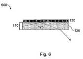
- FIG. 6illustrates a light-emitting device 600 in accordance with another embodiment of the invention.
- a light pipe 125can include a wavelength-converting region which may be localized to specific regions within the light pipe or may extend throughout the light pipe.
- a wavelength-converting regionmay be disposed along the emission surface of the light pipe 125 ; for example, a wavelength-converting layer may be located on the emission surface of the light pipe.
- the light-generating region 110can be configured to generate light that propagates into the light pipe.
- a reflective thermally conductive region 130can partially or completely contact one or more sidewalls of the light pipe.
- the light pipemay also include cooling channels to enable the flow of fluid.
- light generated by region 110can propagate within the light-pipe and be reflected by the reflective thermally conductive region 130 .
- Light from region 110may also be converted by the wavelength-converting region located within or on the light pipe, thereby emitting converted light.
- the reflective thermally conductive regionmay completely surround the sidewalls of the light pipe and thereby ensure that all light is emitted at side 126 of the light pipe.
- light generated by region 110traverses the entire length of the light pipe, and therefore may have ample opportunity to be converted by the wavelength-converting region within the light pipe.
- the length of the light pipemay be tailored to convert a desired portion of the light emitted by the light-generating region so that the combined converted and unconverted light emitted by the light-emitting device 600 possess a desired wavelength spectrum.
- the light pipe 125may posses a length (e.g., greater than about 1 cm, greater than about 3 cm, greater than about 5 cm, or greater than about 10 cm) such that the surface area of the light pipe can provide substantial cooling via contact with the surrounding atmosphere, without the use of a thermally conductive region.
- a reflecting surfacemay still be present on one or more sides of the light pipe, but the reflecting surface need necessarily be part of a thermally conductive region.
- the wavelength-converting regionis incorporated into objects having any other shape. For example, a wavelength-converting region may be incorporated within and/or on a light diffusion panel or a globe.
- FIG. 7illustrates another embodiment of a light-emitting device 700 where the sidewalls of the wavelength-converting region 120 are arranged alongside the sidewalls of one or more light-generating regions 110 .
- light-generating regions 110are LEDs that include active regions 114 .
- insulating layers 186may insulate one or more sides of the LEDs.
- Reflective layers 185are formed on the top surface and outer sidewalls of the LEDs, whereas the inner sidewalls of the LEDs face the wavelength-converting region.
- the reflecting layersmay be formed of a conductive material, and therefore can also serve as contact pads on the top surface of the LEDs; in such a case, insulating layers 186 ensure that the LED sidewalls are electrically insulated from the conductive reflective layers 185 .
- a thermally conductive region 130may be placed in thermal contact with the LEDs and the wavelength-converting region, and the thermally conductive region may be disposed over a support 175 . Furthermore, the thermally conductive region may also include a reflective surface that can reflect impinging light.
- any light generated by the active regions 114 which is not emitted directly into the wavelength-converting region 120can be reflected into the wavelength-converting region by reflective layers 185 and/or the reflective surface of the thermally conductive region 130 .
- some or all of the lightmay be converted by wavelength-converting material and, therefore, light emitted at surface 121 of the wavelength-converting region may include both converted and unconverted light.
- Heat generated by the wavelength-converting region and/or the LEDsmay be extracted by the thermally conductive region, thereby facilitating operation at high power levels.
- the thermally conductive regionmay in turn be in thermal contact with a heat sink (not shown).
- the support 175may also be thermally conductive and can be placed in contact with a heat sink (not shown) thereby enabling the conduction of heat generated in wavelength-converting region 120 and/or LEDs 110 to the thermally conductive region 130 , then through support 175 , and into the heat sink.
- FIGS. 8 a–cillustrate top views of various embodiments of light-emitting device 700 .
- the wavelength-converting region 120is surrounded by the light-generating region 110 .
- light-generating regionsare formed on two or more sides of the wavelength-converting-region but do not surround the entire light-generating regions.
- multiple wavelength-converting regions and light-generating regionsform an alternating array of wavelength-converting regions and light-generating regions.
- FIG. 9illustrates a light-emitting device 900 in accordance with another embodiment of the invention.
- a cavity with an opening 191is formed by cavity walls 190 , and the cavity may be partially or completely filled with a wavelength-converting region 120 .
- One or more light-generating regions 110e.g., LEDs
- Light-generating regionsare positioned within the cavity walls, outside the cavity walls and/or embedded within the walls.
- a thermally conductive region 130surrounds the cavity so that at least a portion of the light-generating regions and the wavelength-converting region are in thermal contact with the thermally conductive region.
- heat extraction and/or conduction from the wavelength-converting regioncan also be provided by conductive poles and/or tubes embedded within the wavelength-converting region.
- light-generating regions 110emit light into wavelength-converting region 120 .
- the generated lightcan be converted by the wavelength-converting region and the converted light can reflect off the cavity walls 190 .
- the cavity wallsmay be configured to allow transmission of unconverted light, but reflect converted light (e.g., dichroic walls).
- Lightcan exit the cavity via opening 191 .
- Thermal management and operation at high powers and brightness of emitted lightcan be enabled as a result of the thermally conductive region 130 which surrounds the cavity and is in thermal contact with the light-generating regions and the wavelength-converting region.
- the thermally conductive regionincludes channels for fluid flow.
- thermally conductive materialcan be incorporated within the wavelength-converting region (e.g., metallic rods, carbon nanotubes)
- the wavelength-converting regionis designed to minimize re-absorption of converted light. For example, this can be accomplished by layering a wavelength-converting material in accordance with known absorption and emission properties of the wavelength-converting material.
- a multilayer wavelength-converting regioncan include several wavelength-converting layers, each which emits light at a different wavelength. In order to optimize the multilayer structure, the layer order from bottom to top can be chosen so that light emitted by lower layers is not substantially reabsorbed by upper layers.
- light channelscan be incorporated into the wavelength-converting region. For example, one or more light channels, that do not include wavelength-converting material, may be formed so as to extend from the opening 191 into the wavelength-converting region 120 . The light channels may be empty or may be filled with a material that has a suitable index of refraction.
- the cavityis not filled with a wavelength-converting region, but rather the wavelength-converting region is located at the opening of the cavity.
- the wavelength-converting regionmay be incorporated into a window located at the opening of the cavity.
- the sides of the cavityare tapered or patterned so as to direct light out of the cavity opening. It should also be appreciated that the cavity may have any shape, and may also include more than one openings, as the invention is not limited so.
- FIG. 10illustrates an embodiment of a multi-layer stack of an LED 1010 that includes a wavelength-converting region.
- wavelength-converting region 120can be incorporated between the active region 114 and a reflective layer 112 formed over a support 175 .
- Reflective layer 112can also be electrically conductive and therefore can serve as an electrical contact for the LED.
- reflective layer 112can serve as a thermally conductive region and therefore aid in the extraction of heat from the wavelength-converting region.
- support 175may also be thermally conductive and can be placed in contact with a heat sink (not shown) thereby enabling the conduction of heat generated in wavelength-converting region 120 , through the reflective layer 112 , then through support 175 , and into the heat sink.
- the wavelength-converting regionmay be patterned so as to enable current injection (and thermal conduction) to the LED multi-layer stack through conductive regions 112 ′.
- the LEDcan additionally, or alternatively, include a current spreading layer (e.g., a transparent metal or a metal oxide) at or near the interface between the wavelength-converting region and doped layer 113 of the LED multi-layer stack.
- a current spreading layere.g., a transparent metal or a metal oxide
- unconverted light from the active regioncan escape the multi-layer stack via emitting surface 118 . Additionally, light from the active region can also be absorbed by the wavelength-converting region and converted to light of another wavelength. Reflecting layer 112 can facilitate directing converted light toward the emission surface 118 , and can also serve as a thermally conductive region in thermal contact with the wavelength-converting region and/or the remainder of the LED multi-layer stack (via conductive region 112 ′).
- FIG. 11illustrates an embodiment of an LED 1010 in accordance with an embodiment of the invention.
- a wavelength-converting regionis incorporated into an electrically and/or thermally conductive layer of the LED multi-layer stack.
- wavelength-converting materialis incorporated into an electrically and/or thermally conductive layer 112 disposed between the doped layer 113 and the support 175 .
- Layer 112may be formed of conductive silver epoxy incorporating wavelength-converting material (e.g., phosphorus particles, nanodots) within, but it should be understood that this is just one example of an electrically and/or thermally conductive layer having a wavelength-converting region within, and other embodiments are possible.
- Layer 112may serve multiple functions, including converting light emitted by the active layer 114 via the wavelength-converting material present therein. Furthermore, layer 112 may also serve as an electrically conductive region that enables current to be injected into the doped layer 113 of the LED. Moreover, layer 112 may also serve as a thermally conductive region for the wavelength-converting material therein and/or the remaining LED multi-layer stack.
- wavelength-converting materialscan be incorporated into larger objects (e.g., panels, 3-dimensional objects) by mixing wavelength-converting materials with a porous material (e.g., foam based materials, porous silica, aerogel).
- the wavelength-converting materialcan be excited remotely using incident light (e.g., using LEDs or lasers) or internally by embedded light-generating regions (e.g., LEDs or lasers).
- incident lighte.g., using LEDs or lasers
- embedded light-generating regionse.g., LEDs or lasers
- the cooling processis a result of the substantially large amount of surface area between the porous material and the surrounding atmosphere, as compared to a non-porous material.
- a heat sink in thermal contact with the structurescan be employed to facilitate operation at high power and brightness of the emitted light.
- the light-emitting devices and structures described in the above embodimentscan be fabricated using a combination of any suitable processing techniques.
- Such processescan include thin film deposition techniques, such as chemical vapor deposition, for depositing various materials, including semiconductors, insulators, and metals. Evaporation and sputtering can be utilized to deposit metals.
- Patterning processessuch as photo-lithography and nano-imprint techniques, may be used to form patterning masks.
- Etching processessuch as dry etching (e.g., reactive ion etching), and wet etching, may be used to pattern layers.
- Coating and spin-coatingcan be used to deposit encapsulants and wavelength-converting regions, such as wavelength-converting materials (e.g., phosphor particles, nanodots) suspended in a secondary material (e.g., epoxy).
- wavelength-converting materialse.g., phosphor particles, nanodots
- injection moldingcan also be used to form wavelength-converting regions.
- Wafer bonding processesmay be used to transfer structures and devices.
- packaging processesmay be used to package the aforementioned light-emitting devices and structures.
- the thermally conductive regioncan conduct heat away from the wavelength-converting region (and, in some cases, also the light-generating region). This enables the light-emitting devices to operate at the high power levels.
- the light-emitting devicemay emit light having a total power greater than 0.5 Watts, greater than 1 Watt, greater than 5 Watts, or greater than 10 Watts. In some cases, the light emitted by the device has a total power of less than 100 Watts, though this should not be construed as a limitation of all embodiments of the invention.
- the desired powerdepends, in part, on the application. These high powers may be maintained for long operating lifetimes, in part, due to conduction of the heat away from the wavelength-converting region by the thermally conductive region.
- operating lifetimerefers to the length of time a device can maintain light emission having at least 50% of the total power of the initial light emission from the device). In some embodiments, the operating lifetimes may be greater than 2,000 hours (e.g., greater than 5,000 hours, greater than 10,000 hours, and greater than 20,000 hours).
Landscapes
- Led Device Packages (AREA)
- Electroluminescent Light Sources (AREA)
Abstract
Description
Claims (60)
Priority Applications (4)
| Application Number | Priority Date | Filing Date | Title |
|---|---|---|---|
| US11/238,667US7196354B1 (en) | 2005-09-29 | 2005-09-29 | Wavelength-converting light-emitting devices |
| EP06751759.9AEP1938380A4 (en) | 2005-09-29 | 2006-04-28 | WAVELENGTH CONVERTING ELECTROLUMINESCENT DEVICE |
| PCT/US2006/016226WO2007040627A1 (en) | 2005-09-29 | 2006-04-28 | Wavelength-converting light-emitting devices |
| CN2006800447502ACN101346818B (en) | 2005-09-29 | 2006-04-28 | Wavelength-converting light-emitting devices |
Applications Claiming Priority (1)
| Application Number | Priority Date | Filing Date | Title |
|---|---|---|---|
| US11/238,667US7196354B1 (en) | 2005-09-29 | 2005-09-29 | Wavelength-converting light-emitting devices |
Publications (1)
| Publication Number | Publication Date |
|---|---|
| US7196354B1true US7196354B1 (en) | 2007-03-27 |
Family
ID=37886057
Family Applications (1)
| Application Number | Title | Priority Date | Filing Date |
|---|---|---|---|
| US11/238,667Active2025-10-24US7196354B1 (en) | 2005-09-29 | 2005-09-29 | Wavelength-converting light-emitting devices |
Country Status (4)
| Country | Link |
|---|---|
| US (1) | US7196354B1 (en) |
| EP (1) | EP1938380A4 (en) |
| CN (1) | CN101346818B (en) |
| WO (1) | WO2007040627A1 (en) |
Cited By (95)
| Publication number | Priority date | Publication date | Assignee | Title |
|---|---|---|---|---|
| US20060121642A1 (en)* | 2004-03-31 | 2006-06-08 | Yu-Chuan Liu | Manufacturing process of light-emitting device |
| US20070164268A1 (en)* | 2005-12-30 | 2007-07-19 | Curran John W | Method and apparatus for providing a light source that combines different color leds |
| US20070291490A1 (en)* | 2006-06-15 | 2007-12-20 | Arosh Baroky Tajul | Light emitting device having a metal can package for improved heat dissipation |
| US20080001161A1 (en)* | 2006-06-28 | 2008-01-03 | Kobayashi Nobuhiko P | Utilizing nanowire for generating white light |
| US20080169753A1 (en)* | 2007-01-11 | 2008-07-17 | Motorola, Inc. | Light emissive printed article printed with quantum dot ink |
| US20080170397A1 (en)* | 2005-12-30 | 2008-07-17 | John Curran | Signal light using phosphor coated leds |
| US20080179609A1 (en)* | 2006-12-22 | 2008-07-31 | Philips Lumileds Lighting Company, Llc | Light emitting device including a filter |
| WO2008149276A1 (en)* | 2007-06-08 | 2008-12-11 | Koninklijke Philips Electronics N.V. | Light output device |
| US20090034230A1 (en)* | 2007-07-31 | 2009-02-05 | Luminus Devices, Inc. | Illumination assembly including wavelength converting material having spatially varying density |
| US20090034292A1 (en)* | 2007-07-31 | 2009-02-05 | Luminus Devices, Inc. | Illumination assembly including wavelength converting material |
| US20090040745A1 (en)* | 2007-05-08 | 2009-02-12 | Luminus Devices, Inc. | Light emitting devices including wavelength converting material |
| US20090052158A1 (en)* | 2007-08-23 | 2009-02-26 | Philips Lumileds Lighting Company, Llc | Light Source Including Reflective Wavelength-Converting Layer |
| US20090059554A1 (en)* | 2007-08-28 | 2009-03-05 | Motorola, Inc. | Apparatus for selectively backlighting a material |
| WO2009031084A1 (en)* | 2007-09-04 | 2009-03-12 | Koninklijke Philips Electronics N.V. | Light output device |
| WO2009066206A1 (en)* | 2007-11-19 | 2009-05-28 | Koninklijke Philips Electronics N.V. | Light source and illumination system having a predefined external appearance |
| US20090152567A1 (en)* | 2006-03-07 | 2009-06-18 | Mark Comerford | Article including semiconductor nanocrystals |
| WO2009076921A1 (en)* | 2007-12-19 | 2009-06-25 | Osram Opto Semiconductors Gmbh | Optoelectronic component with cooling element |
| US20090162011A1 (en)* | 2006-03-07 | 2009-06-25 | Seth Coe-Sullivan | Compositions, optical component, system including an optical component, devices, and other products |
| WO2009095662A1 (en)* | 2008-01-28 | 2009-08-06 | Photonstar Led Limited | Light emitting module with optically-transparent thermally-conductive element |
| WO2009095007A1 (en)* | 2008-01-31 | 2009-08-06 | Osram Opto Semiconductors Gmbh | Radiation-emitting device |
| US20090236619A1 (en)* | 2008-03-19 | 2009-09-24 | Arpan Chakroborty | Light Emitting Diodes with Light Filters |
| US20090244923A1 (en)* | 2006-04-26 | 2009-10-01 | Koninklijke Philips Electronics N.V. | Light delivery device with improved conversion element |
| US20090302345A1 (en)* | 2008-06-06 | 2009-12-10 | Bill Chuang | Led lamp module and fabrication method thereof |
| DE102009018087A1 (en) | 2008-04-30 | 2009-12-17 | Ledon Lighting Jennersdorf Gmbh | Light-emitting diode with increased color stability |
| US20090309114A1 (en)* | 2008-01-16 | 2009-12-17 | Luminus Devices, Inc. | Wavelength converting light-emitting devices and methods of making the same |
| US20100033947A1 (en)* | 2008-08-06 | 2010-02-11 | Kismart Corp. | Enhanced Wavelength-Converting Structure |
| US20100051996A1 (en)* | 2008-08-29 | 2010-03-04 | Chia-Liang Hsu | Light-emitting semiconductor device and package thereof |
| US20100059777A1 (en)* | 2006-12-05 | 2010-03-11 | Koninklijke Philips Electronics N.V. | Illumination device, particularly with luminescent ceramics |
| WO2010027650A1 (en)* | 2008-09-04 | 2010-03-11 | 3M Innovative Properties Company | Light source with improved monochromaticity |
| WO2009158138A3 (en)* | 2008-06-26 | 2010-03-18 | 3M Innovative Properties Company | Semiconductor light converting construction |
| WO2009155907A3 (en)* | 2008-06-25 | 2010-03-18 | Osram Opto Semiconductors Gmbh | Heat dissipation system for a conversion element and corresponding lighting device |
| WO2009115998A3 (en)* | 2008-03-21 | 2010-03-25 | Koninklijke Philips Electronics N.V. | A luminous device |
| WO2010035206A1 (en)* | 2008-09-25 | 2010-04-01 | Koninklijke Philips Electronics N.V. | Coated light emitting device and method for coating thereof |
| US20100095057A1 (en)* | 2008-10-15 | 2010-04-15 | Seagate Technology Llc | Non-volatile resistive sense memory on-chip cache |
| DE102008057720A1 (en)* | 2008-11-17 | 2010-05-20 | Osram Opto Semiconductors Gmbh | Radiation emitting device i.e. white light emitting device, has radiation converting layer provided with organic radiation converting luminescent material and arranged at distance from radiation emitting functional layer |
| US20100149815A1 (en)* | 2008-10-17 | 2010-06-17 | Luminus Devices, Inc. | Remote lighting assemblies and methods |
| WO2010067291A1 (en) | 2008-12-11 | 2010-06-17 | Koninklijke Philips Electronics N.V. | Adjustable color lamp with movable color conversion layers |
| WO2010084451A1 (en)* | 2009-01-21 | 2010-07-29 | Koninklijke Philips Electronics N.V. | Light source comprising a light recycling device and corresponding light recycling device |
| US20100219767A1 (en)* | 2008-09-24 | 2010-09-02 | Luminus Devices, Inc. | Light-emitting device including independently electrically addressable sections |
| CN101936508A (en)* | 2009-06-29 | 2011-01-05 | 新高创意科技有限公司 | Light source wavelength modulation device |
| EP2270884A1 (en)* | 2009-06-30 | 2011-01-05 | Acpa Energy Conversion Devices Co.,Ltd. | Wavelength conversion device for LED's or solar cells |
| US20110044026A1 (en)* | 2008-05-07 | 2011-02-24 | Koninklijke Philips Electronics N.V. | Illumination device with led with a self-supporting grid containing luminescent material and method of making the self-supporting grid |
| US20110084292A1 (en)* | 2009-10-01 | 2011-04-14 | Luminus Devices, Inc. | Arrays of light emitting devices |
| US20110101402A1 (en)* | 2008-06-26 | 2011-05-05 | Jun-Ying Zhang | Semiconductor light converting construction |
| US20110101382A1 (en)* | 2008-06-26 | 2011-05-05 | Smith Terry L | Light converting construction |
| US20110114970A1 (en)* | 2008-04-23 | 2011-05-19 | Agency For Science, Technology And Research | Light emitting diode structure, a lamp device and a method of forming a light emitting diode structure |
| US20110117686A1 (en)* | 2008-06-26 | 2011-05-19 | Jun-Ying Zhang | Method of fabricating light extractor |
| US20110133224A1 (en)* | 2008-08-05 | 2011-06-09 | Photonstar Led Limited | Thermally optimised led chip-on-board module |
| US20110140128A1 (en)* | 2008-09-04 | 2011-06-16 | Leatherdale Catherine A | Monochromatic light source with high aspect ratio |
| US20110139240A1 (en)* | 2009-12-15 | 2011-06-16 | First Solar, Inc. | Photovoltaic window layer |
| US20110150019A1 (en)* | 2008-09-04 | 2011-06-23 | Leatherdale Catherine A | Monochromatic light source |
| US20110150020A1 (en)* | 2008-09-04 | 2011-06-23 | 3M Innovative Properties Company | Ii-vi mqw vscel on a heat sink optically pumped by a gan ld |
| US20110210361A1 (en)* | 2006-07-04 | 2011-09-01 | Epistar Corporation | High efficient phosphor-converted light emitting diode |
| WO2012015556A1 (en)* | 2010-07-29 | 2012-02-02 | Cree, Inc. | Lighting devices that comprise one or more solid state light emitters |
| US20120039072A1 (en)* | 2008-12-18 | 2012-02-16 | Alfred Lell | Luminous Means and Projector Comprising at Least One Luminous Means of this Type |
| WO2012060856A1 (en)* | 2010-11-01 | 2012-05-10 | Tyco Electronics Corporation | Optic assembly utilizing quantum dots |
| WO2012091975A1 (en)* | 2010-12-29 | 2012-07-05 | 3M Innovative Properties Company | Phosphor reflector assembly for remote phosphor led device |
| US20120256200A1 (en)* | 2010-10-15 | 2012-10-11 | Cree, Inc. | High efficiency leds |
| WO2012164283A1 (en)* | 2011-05-31 | 2012-12-06 | Nanoco Technologies Limited | Semiconductor nanoparticle - containing materials and light emitting devices incorporating the same |
| US8405063B2 (en) | 2007-07-23 | 2013-03-26 | Qd Vision, Inc. | Quantum dot light enhancement substrate and lighting device including same |
| CN102305386B (en)* | 2008-01-29 | 2013-06-12 | 深圳市绎立锐光科技开发有限公司 | Light source structure and method for improving light conversion efficiency based on fluorescent powder |
| US20130341590A1 (en)* | 2012-06-25 | 2013-12-26 | Cree, Inc. | Quantum Dot Narrow-Band Downconverters for High Efficiency LEDs |
| US20140084317A1 (en)* | 2012-09-24 | 2014-03-27 | Kwang Chil LEE | Ultraviolet light emitting device |
| JP2014140014A (en)* | 2012-12-18 | 2014-07-31 | Toyoda Gosei Co Ltd | Light emitting device and manufacturing method of the same |
| TWI452738B (en)* | 2010-11-23 | 2014-09-11 | Advanced Optoelectronic Tech | Led package and method for manufacturing the same |
| CN103353091B (en)* | 2008-01-29 | 2014-11-05 | 深圳市绎立锐光科技开发有限公司 | Light source structure based on light conversion efficiency increment through fluorescent powder |
| US20150028365A1 (en)* | 2013-07-24 | 2015-01-29 | Juanita N. Kurtin | Highly refractive, transparent thermal conductors for better heat dissipation and light extraction in white leds |
| US9018619B2 (en) | 2006-10-09 | 2015-04-28 | Cree, Inc. | Quantum wells for light conversion |
| US9140844B2 (en) | 2008-05-06 | 2015-09-22 | Qd Vision, Inc. | Optical components, systems including an optical component, and devices |
| US9147816B2 (en) | 2012-08-24 | 2015-09-29 | Luminus Devices, Inc. | Wavelength converting material deposition methods and associated articles |
| US9167659B2 (en) | 2008-05-06 | 2015-10-20 | Qd Vision, Inc. | Solid state lighting devices including quantum confined semiconductor nanoparticles, an optical component for a solid state lighting device, and methods |
| US9207385B2 (en) | 2008-05-06 | 2015-12-08 | Qd Vision, Inc. | Lighting systems and devices including same |
| WO2015185549A1 (en)* | 2014-06-05 | 2015-12-10 | Osram Opto Semiconductors Gmbh | Optoelectronic component |
| US9223081B2 (en) | 2011-04-05 | 2015-12-29 | Lg Innotek Co., Ltd. | Optical member and display device including the same |
| US9236550B2 (en) | 2010-03-19 | 2016-01-12 | Micron Technology, Inc. | Light emitting diodes with enhanced thermal sinking and associated methods of operation |
| US20160149090A1 (en)* | 2013-06-24 | 2016-05-26 | Osram Opto Semiconductors Gmbh | Radiation-Emitting Optoelectronic Device |
| JP2016225581A (en)* | 2015-06-04 | 2016-12-28 | 日本電気硝子株式会社 | Wavelength conversion member and light-emitting device including the same |
| US20170052362A1 (en)* | 2015-08-21 | 2017-02-23 | Delta Electronics, Inc. | Phosphor wheel and wavelength converting device applying the same |
| JP2017085039A (en)* | 2015-10-30 | 2017-05-18 | 日本電気硝子株式会社 | Method of manufacturing wavelength conversion element and wavelength conversion element and light-emitting device |
| US20170139113A1 (en)* | 2014-06-05 | 2017-05-18 | Philips Lighting Holding B.V. | Luminescence concentrator with increased efficiency |
| JP2017085038A (en)* | 2015-10-30 | 2017-05-18 | 日本電気硝子株式会社 | Method of manufacturing wavelength conversion element |
| US20170167710A1 (en)* | 2014-05-13 | 2017-06-15 | Appotronics China Corporation | Wavelength conversion device, light source system and projection system |
| JP2017194706A (en)* | 2012-08-02 | 2017-10-26 | 日亜化学工業株式会社 | Method for manufacturing wavelength converting device |
| WO2018002809A1 (en)* | 2016-06-29 | 2018-01-04 | Sabic Global Technologies B.V. | Fabrication of phosphor film with heat dissipation film |
| US9864121B2 (en) | 2011-11-22 | 2018-01-09 | Samsung Electronics Co., Ltd. | Stress-resistant component for use with quantum dots |
| US9874674B2 (en) | 2006-03-07 | 2018-01-23 | Samsung Electronics Co., Ltd. | Compositions, optical component, system including an optical component, devices, and other products |
| JP2018185542A (en)* | 2011-10-25 | 2018-11-22 | ショット アクチエンゲゼルシャフトSchott AG | Optical converter for high luminance |
| DE102017220940A1 (en)* | 2017-11-23 | 2019-05-23 | Osram Gmbh | Converter for a conversion light with heat conducting layer |
| US10374137B2 (en)* | 2014-03-11 | 2019-08-06 | Osram Gmbh | Light converter assemblies with enhanced heat dissipation |
| JP2021022590A (en)* | 2019-07-24 | 2021-02-18 | 京セラ株式会社 | Optical device package and optical device |
| CN112666780A (en)* | 2019-10-15 | 2021-04-16 | 台达电子工业股份有限公司 | Wavelength conversion device |
| CN113300211A (en)* | 2021-06-24 | 2021-08-24 | 西安嘉合超亿光电科技有限公司 | Semiconductor laser packaging structure and preparation method thereof |
| US11367817B2 (en) | 2018-03-23 | 2022-06-21 | Osram Oled Gmbh | Optoelectronic component including a reflective potting compound, and its production method |
| US11670666B2 (en) | 2019-10-08 | 2023-06-06 | Luminus, Inc. | Light-emitting systems with close-packed LEDs and/or electrically isolated substrates and methods of making and/or operating the same |
| US12304172B1 (en)* | 2024-04-19 | 2025-05-20 | China Jiliang University | Multilayered fluorescent wafer for laser lighting and display, and method of manufacturing |
Families Citing this family (14)
| Publication number | Priority date | Publication date | Assignee | Title |
|---|---|---|---|---|
| WO2008105428A1 (en)* | 2007-02-27 | 2008-09-04 | Kyocera Corporation | Light-emitting device |
| US7855394B2 (en)* | 2009-06-18 | 2010-12-21 | Bridgelux, Inc. | LED array package covered with a highly thermal conductive plate |
| US8294168B2 (en)* | 2010-06-04 | 2012-10-23 | Samsung Electronics Co., Ltd. | Light source module using quantum dots, backlight unit employing the light source module, display apparatus, and illumination apparatus |
| CN103026126B (en)* | 2010-09-21 | 2015-02-25 | 日本电气株式会社 | Phosphor-coated light emitting device |
| CN103299422B (en) | 2010-12-29 | 2016-11-02 | 3M创新有限公司 | Remote Phosphor LED Unit with Broadband Output and Controllable Color |
| US8912562B2 (en) | 2010-12-29 | 2014-12-16 | 3M Innovative Properties Company | Remote phosphor LED constructions |
| WO2013023662A1 (en)* | 2011-08-17 | 2013-02-21 | Martin Professional A/S | Illumination device with fluid cooled converting material |
| CN102280564A (en)* | 2011-08-19 | 2011-12-14 | 华南师范大学 | Light emitting diode (LED) possessing phosphor heat dissipating layer |
| CN102263195A (en)* | 2011-08-19 | 2011-11-30 | 华南师范大学 | Power Type Light Emitting Diode Using Phosphor Powder Thermal Conduction Structure |
| CN102437272B (en)* | 2011-11-25 | 2014-01-01 | 深圳市光峰光电技术有限公司 | Wavelength conversion device and light emitting device |
| CN104879713A (en)* | 2014-03-02 | 2015-09-02 | 陈雁北 | Wavelength converter and light-emitting device |
| CN105375329A (en)* | 2014-08-08 | 2016-03-02 | 深圳市绎立锐光科技开发有限公司 | Wavelength conversion unit, preparation method thereof, related wavelength conversion sheet and light emitting device |
| TWI705214B (en)* | 2015-10-09 | 2020-09-21 | 日商松下知識產權經營股份有限公司 | Lighting device |
| US10193030B2 (en)* | 2016-08-08 | 2019-01-29 | General Electric Company | Composite materials having red emitting phosphors |
Citations (49)
| Publication number | Priority date | Publication date | Assignee | Title |
|---|---|---|---|---|
| US4729076A (en) | 1984-11-15 | 1988-03-01 | Tsuzawa Masami | Signal light unit having heat dissipating function |
| US5113232A (en) | 1990-07-31 | 1992-05-12 | Eastman Kodak Company | LED array chips with thermal conductor |
| US6045240A (en) | 1996-06-27 | 2000-04-04 | Relume Corporation | LED lamp assembly with means to conduct heat away from the LEDS |
| US6265820B1 (en) | 1998-01-29 | 2001-07-24 | Emagin Corporation | Heat removal system for use in organic light emitting diode displays having high brightness |
| US6335548B1 (en) | 1999-03-15 | 2002-01-01 | Gentex Corporation | Semiconductor radiation emitter package |
| US6340824B1 (en) | 1997-09-01 | 2002-01-22 | Kabushiki Kaisha Toshiba | Semiconductor light emitting device including a fluorescent material |
| US6375340B1 (en) | 1999-07-08 | 2002-04-23 | Patent-Treuhand-Gesellschaft Fuer Elektrische Gluehlampen Mbh | Led component group with heat dissipating support |
| US6388264B1 (en) | 1997-03-28 | 2002-05-14 | Benedict G Pace | Optocoupler package being hermetically sealed |
| US6410940B1 (en) | 2000-06-15 | 2002-06-25 | Kansas State University Research Foundation | Micro-size LED and detector arrays for minidisplay, hyper-bright light emitting diodes, lighting, and UV detector and imaging sensor applications |
| US6450664B1 (en) | 1999-10-01 | 2002-09-17 | Stockeryale (Irl) Limited | Linear illumination unit having plurality of LEDs |
| US6452217B1 (en) | 2000-06-30 | 2002-09-17 | General Electric Company | High power LED lamp structure using phase change cooling enhancements for LED lighting products |
| US6476549B2 (en) | 2000-10-26 | 2002-11-05 | Mu-Chin Yu | Light emitting diode with improved heat dissipation |
| US6475819B2 (en) | 1998-06-29 | 2002-11-05 | Osram Opto Semiconductors Gmbh & Co. Ohg | Method for formation and production of matrices of high density light emitting diodes |
| US6480389B1 (en) | 2002-01-04 | 2002-11-12 | Opto Tech Corporation | Heat dissipation structure for solid-state light emitting device package |
| US6481874B2 (en) | 2001-03-29 | 2002-11-19 | Gelcore Llc | Heat dissipation system for high power LED lighting system |
| US6501103B1 (en) | 2001-10-23 | 2002-12-31 | Lite-On Electronics, Inc. | Light emitting diode assembly with low thermal resistance |
| US6504180B1 (en) | 1998-07-28 | 2003-01-07 | Imec Vzw And Vrije Universiteit | Method of manufacturing surface textured high-efficiency radiating devices and devices obtained therefrom |
| US6504181B2 (en) | 1999-12-21 | 2003-01-07 | Kabushiki Kaisha Toshiba | Semiconductor light emitting element and manufacturing method thereof |
| US6518600B1 (en) | 2000-11-17 | 2003-02-11 | General Electric Company | Dual encapsulation for an LED |
| US20030141563A1 (en) | 2002-01-28 | 2003-07-31 | Bily Wang | Light emitting diode package with fluorescent cover |
| US6608332B2 (en) | 1996-07-29 | 2003-08-19 | Nichia Kagaku Kogyo Kabushiki Kaisha | Light emitting device and display |
| US6624491B2 (en) | 1998-06-30 | 2003-09-23 | Osram Opto Semiconductors Gmbh & Co. | Diode housing |
| US6642618B2 (en) | 2000-12-21 | 2003-11-04 | Lumileds Lighting U.S., Llc | Light-emitting device and production thereof |
| US6690268B2 (en) | 2000-03-02 | 2004-02-10 | Donnelly Corporation | Video mirror systems incorporating an accessory module |
| US20040124002A1 (en) | 1999-12-13 | 2004-07-01 | Lamina Ceramics, Inc. | Method and structures for enhanced temperature control of high power components on multilayer LTCC and LTCC-M boards |
| US6759723B2 (en) | 2001-01-10 | 2004-07-06 | Silverbrook Research Pty Ltd | Light emitting semiconductor package |
| US20040150997A1 (en) | 2003-01-27 | 2004-08-05 | 3M Innovative Properties Company | Phosphor based light sources having a reflective polarizer |
| US6791259B1 (en) | 1998-11-30 | 2004-09-14 | General Electric Company | Solid state illumination system containing a light emitting diode, a light scattering material and a luminescent material |
| US20040207319A1 (en) | 2003-04-15 | 2004-10-21 | Erchak Alexei A. | Light emitting devices |
| US20040207323A1 (en) | 2003-04-15 | 2004-10-21 | Erchak Alexei A. | Light emitting devices |
| US6812503B2 (en) | 2001-11-29 | 2004-11-02 | Highlink Technology Corporation | Light-emitting device with improved reliability |
| US20040222433A1 (en) | 2003-05-05 | 2004-11-11 | Lamina Ceramics | Light emitting diodes packaged for high temperature operation |
| US6828724B2 (en) | 2000-05-17 | 2004-12-07 | Cambridge Display Technology Limited | Light-emitting devices |
| US6849876B1 (en) | 2004-05-31 | 2005-02-01 | Excel Cell Electronic Co., Ltd. | Light emitting device |
| US6864571B2 (en) | 2003-07-07 | 2005-03-08 | Gelcore Llc | Electronic devices and methods for making same using nanotube regions to assist in thermal heat-sinking |
| US6881980B1 (en) | 2004-06-17 | 2005-04-19 | Chunghwa Picture Tubes, Ltd. | Package structure of light emitting diode |
| US6885033B2 (en) | 2003-03-10 | 2005-04-26 | Cree, Inc. | Light emitting devices for light conversion and methods and semiconductor chips for fabricating the same |
| US6891203B2 (en) | 2001-01-10 | 2005-05-10 | Toyoda Gosei Co., Ltd. | Light emitting device |
| US20050110036A1 (en) | 2003-11-20 | 2005-05-26 | Park Joung U. | LED package |
| US6900587B2 (en) | 2001-06-28 | 2005-05-31 | Toyoda Gosei Co., Ltd. | Light-emitting diode |
| US20050133808A1 (en) | 2003-09-11 | 2005-06-23 | Kyocera Corporation | Package for housing light-emitting element, light-emitting apparatus and illumination apparatus |
| US6914261B2 (en) | 2003-10-10 | 2005-07-05 | Lambda Opto Technology Co., Ltd. | Light emitting diode module |
| US6943379B2 (en) | 2002-04-04 | 2005-09-13 | Toyoda Gosei Co., Ltd. | Light emitting diode |
| US20050211991A1 (en) | 2004-03-26 | 2005-09-29 | Kyocera Corporation | Light-emitting apparatus and illuminating apparatus |
| US6956247B1 (en) | 2004-05-26 | 2005-10-18 | Lumileds Lighting U.S., Llc | Semiconductor light emitting device including photonic band gap material and luminescent material |
| US20050231983A1 (en) | 2002-08-23 | 2005-10-20 | Dahm Jonathan S | Method and apparatus for using light emitting diodes |
| US6964501B2 (en) | 2002-12-24 | 2005-11-15 | Altman Stage Lighting Co., Ltd. | Peltier-cooled LED lighting assembly |
| US20050258438A1 (en) | 2004-05-21 | 2005-11-24 | Gelcore, Llc | Light emitting diode apparatuses with heat pipes for thermal management |
| US7091653B2 (en)* | 2003-01-27 | 2006-08-15 | 3M Innovative Properties Company | Phosphor based light sources having a non-planar long pass reflector |
Family Cites Families (3)
| Publication number | Priority date | Publication date | Assignee | Title |
|---|---|---|---|---|
| US6366018B1 (en)* | 1998-10-21 | 2002-04-02 | Sarnoff Corporation | Apparatus for performing wavelength-conversion using phosphors with light emitting diodes |
| WO2005038935A1 (en)* | 2003-10-15 | 2005-04-28 | Nichia Corporation | Light-emitting device |
| CN1652642A (en)* | 2004-02-03 | 2005-08-10 | 悠景科技股份有限公司 | Substrate assembly of display device and making method thereof |
- 2005
- 2005-09-29USUS11/238,667patent/US7196354B1/enactiveActive
- 2006
- 2006-04-28EPEP06751759.9Apatent/EP1938380A4/ennot_activeWithdrawn
- 2006-04-28CNCN2006800447502Apatent/CN101346818B/ennot_activeExpired - Fee Related
- 2006-04-28WOPCT/US2006/016226patent/WO2007040627A1/enactiveApplication Filing
Patent Citations (51)
| Publication number | Priority date | Publication date | Assignee | Title |
|---|---|---|---|---|
| US4729076A (en) | 1984-11-15 | 1988-03-01 | Tsuzawa Masami | Signal light unit having heat dissipating function |
| US5113232A (en) | 1990-07-31 | 1992-05-12 | Eastman Kodak Company | LED array chips with thermal conductor |
| US6045240A (en) | 1996-06-27 | 2000-04-04 | Relume Corporation | LED lamp assembly with means to conduct heat away from the LEDS |
| US6608332B2 (en) | 1996-07-29 | 2003-08-19 | Nichia Kagaku Kogyo Kabushiki Kaisha | Light emitting device and display |
| US6388264B1 (en) | 1997-03-28 | 2002-05-14 | Benedict G Pace | Optocoupler package being hermetically sealed |
| US6340824B1 (en) | 1997-09-01 | 2002-01-22 | Kabushiki Kaisha Toshiba | Semiconductor light emitting device including a fluorescent material |
| US6265820B1 (en) | 1998-01-29 | 2001-07-24 | Emagin Corporation | Heat removal system for use in organic light emitting diode displays having high brightness |
| US6475819B2 (en) | 1998-06-29 | 2002-11-05 | Osram Opto Semiconductors Gmbh & Co. Ohg | Method for formation and production of matrices of high density light emitting diodes |
| US6624491B2 (en) | 1998-06-30 | 2003-09-23 | Osram Opto Semiconductors Gmbh & Co. | Diode housing |
| US6504180B1 (en) | 1998-07-28 | 2003-01-07 | Imec Vzw And Vrije Universiteit | Method of manufacturing surface textured high-efficiency radiating devices and devices obtained therefrom |
| US6791259B1 (en) | 1998-11-30 | 2004-09-14 | General Electric Company | Solid state illumination system containing a light emitting diode, a light scattering material and a luminescent material |
| US6335548B1 (en) | 1999-03-15 | 2002-01-01 | Gentex Corporation | Semiconductor radiation emitter package |
| US6375340B1 (en) | 1999-07-08 | 2002-04-23 | Patent-Treuhand-Gesellschaft Fuer Elektrische Gluehlampen Mbh | Led component group with heat dissipating support |
| US6450664B1 (en) | 1999-10-01 | 2002-09-17 | Stockeryale (Irl) Limited | Linear illumination unit having plurality of LEDs |
| US20040124002A1 (en) | 1999-12-13 | 2004-07-01 | Lamina Ceramics, Inc. | Method and structures for enhanced temperature control of high power components on multilayer LTCC and LTCC-M boards |
| US6504181B2 (en) | 1999-12-21 | 2003-01-07 | Kabushiki Kaisha Toshiba | Semiconductor light emitting element and manufacturing method thereof |
| US6627521B2 (en) | 1999-12-21 | 2003-09-30 | Kabushiki Kaisha Toshiba | Semiconductor light emitting element and manufacturing method thereof |
| US6690268B2 (en) | 2000-03-02 | 2004-02-10 | Donnelly Corporation | Video mirror systems incorporating an accessory module |
| US6828724B2 (en) | 2000-05-17 | 2004-12-07 | Cambridge Display Technology Limited | Light-emitting devices |
| US6410940B1 (en) | 2000-06-15 | 2002-06-25 | Kansas State University Research Foundation | Micro-size LED and detector arrays for minidisplay, hyper-bright light emitting diodes, lighting, and UV detector and imaging sensor applications |
| US6452217B1 (en) | 2000-06-30 | 2002-09-17 | General Electric Company | High power LED lamp structure using phase change cooling enhancements for LED lighting products |
| US6476549B2 (en) | 2000-10-26 | 2002-11-05 | Mu-Chin Yu | Light emitting diode with improved heat dissipation |
| US6518600B1 (en) | 2000-11-17 | 2003-02-11 | General Electric Company | Dual encapsulation for an LED |
| US6642618B2 (en) | 2000-12-21 | 2003-11-04 | Lumileds Lighting U.S., Llc | Light-emitting device and production thereof |
| US6759723B2 (en) | 2001-01-10 | 2004-07-06 | Silverbrook Research Pty Ltd | Light emitting semiconductor package |
| US6891203B2 (en) | 2001-01-10 | 2005-05-10 | Toyoda Gosei Co., Ltd. | Light emitting device |
| US6481874B2 (en) | 2001-03-29 | 2002-11-19 | Gelcore Llc | Heat dissipation system for high power LED lighting system |
| US6900587B2 (en) | 2001-06-28 | 2005-05-31 | Toyoda Gosei Co., Ltd. | Light-emitting diode |
| US6501103B1 (en) | 2001-10-23 | 2002-12-31 | Lite-On Electronics, Inc. | Light emitting diode assembly with low thermal resistance |
| US6812503B2 (en) | 2001-11-29 | 2004-11-02 | Highlink Technology Corporation | Light-emitting device with improved reliability |
| US6480389B1 (en) | 2002-01-04 | 2002-11-12 | Opto Tech Corporation | Heat dissipation structure for solid-state light emitting device package |
| US20030141563A1 (en) | 2002-01-28 | 2003-07-31 | Bily Wang | Light emitting diode package with fluorescent cover |
| US6943379B2 (en) | 2002-04-04 | 2005-09-13 | Toyoda Gosei Co., Ltd. | Light emitting diode |
| US20050231983A1 (en) | 2002-08-23 | 2005-10-20 | Dahm Jonathan S | Method and apparatus for using light emitting diodes |
| US6964501B2 (en) | 2002-12-24 | 2005-11-15 | Altman Stage Lighting Co., Ltd. | Peltier-cooled LED lighting assembly |
| US7091653B2 (en)* | 2003-01-27 | 2006-08-15 | 3M Innovative Properties Company | Phosphor based light sources having a non-planar long pass reflector |
| US20040150997A1 (en) | 2003-01-27 | 2004-08-05 | 3M Innovative Properties Company | Phosphor based light sources having a reflective polarizer |
| US6885033B2 (en) | 2003-03-10 | 2005-04-26 | Cree, Inc. | Light emitting devices for light conversion and methods and semiconductor chips for fabricating the same |
| US20040207319A1 (en) | 2003-04-15 | 2004-10-21 | Erchak Alexei A. | Light emitting devices |
| US20050258435A1 (en) | 2003-04-15 | 2005-11-24 | Luminus Devices, Inc., A Delaware Corporation | Light-emitting devices |
| US20040207323A1 (en) | 2003-04-15 | 2004-10-21 | Erchak Alexei A. | Light emitting devices |
| US20040222433A1 (en) | 2003-05-05 | 2004-11-11 | Lamina Ceramics | Light emitting diodes packaged for high temperature operation |
| US6864571B2 (en) | 2003-07-07 | 2005-03-08 | Gelcore Llc | Electronic devices and methods for making same using nanotube regions to assist in thermal heat-sinking |
| US20050133808A1 (en) | 2003-09-11 | 2005-06-23 | Kyocera Corporation | Package for housing light-emitting element, light-emitting apparatus and illumination apparatus |
| US6914261B2 (en) | 2003-10-10 | 2005-07-05 | Lambda Opto Technology Co., Ltd. | Light emitting diode module |
| US20050110036A1 (en) | 2003-11-20 | 2005-05-26 | Park Joung U. | LED package |
| US20050211991A1 (en) | 2004-03-26 | 2005-09-29 | Kyocera Corporation | Light-emitting apparatus and illuminating apparatus |
| US20050258438A1 (en) | 2004-05-21 | 2005-11-24 | Gelcore, Llc | Light emitting diode apparatuses with heat pipes for thermal management |
| US6956247B1 (en) | 2004-05-26 | 2005-10-18 | Lumileds Lighting U.S., Llc | Semiconductor light emitting device including photonic band gap material and luminescent material |
| US6849876B1 (en) | 2004-05-31 | 2005-02-01 | Excel Cell Electronic Co., Ltd. | Light emitting device |
| US6881980B1 (en) | 2004-06-17 | 2005-04-19 | Chunghwa Picture Tubes, Ltd. | Package structure of light emitting diode |
Non-Patent Citations (1)
| Title |
|---|
| "NeoPac sets new standard with 500 lumen LED lighting", LEDs Magazine, http://www.ledsmagazine.com/press/9495, Date announced Jul. 5, 2005, Date of website printout Jan. 23, 2006. |
Cited By (196)
| Publication number | Priority date | Publication date | Assignee | Title |
|---|---|---|---|---|
| US20060121642A1 (en)* | 2004-03-31 | 2006-06-08 | Yu-Chuan Liu | Manufacturing process of light-emitting device |
| US20070164268A1 (en)* | 2005-12-30 | 2007-07-19 | Curran John W | Method and apparatus for providing a light source that combines different color leds |
| US7602057B2 (en) | 2005-12-30 | 2009-10-13 | Dialight Corporation | Signal light using phosphor coated LEDs |
| US20090321754A1 (en)* | 2005-12-30 | 2009-12-31 | Curran John W | Signal light using phosphor coated leds |
| US7973402B2 (en) | 2005-12-30 | 2011-07-05 | Dialight Corporation | LED light using phosphor coated LEDs |
| US20080170397A1 (en)* | 2005-12-30 | 2008-07-17 | John Curran | Signal light using phosphor coated leds |
| US8432029B2 (en) | 2005-12-30 | 2013-04-30 | Dialight Corporation | Signal light using phosphor coated LEDs |
| US20080186700A1 (en)* | 2005-12-30 | 2008-08-07 | Curran John W | Signal light using phosphor coated leds |
| US7918582B2 (en) | 2005-12-30 | 2011-04-05 | Dialight Corporation | Signal light using phosphor coated LEDs |
| US7777322B2 (en)* | 2005-12-30 | 2010-08-17 | Dialight Corporation | Apparatus for providing a light source that combines different color LEDS |
| US20090162011A1 (en)* | 2006-03-07 | 2009-06-25 | Seth Coe-Sullivan | Compositions, optical component, system including an optical component, devices, and other products |
| US8718437B2 (en) | 2006-03-07 | 2014-05-06 | Qd Vision, Inc. | Compositions, optical component, system including an optical component, devices, and other products |
| US9874674B2 (en) | 2006-03-07 | 2018-01-23 | Samsung Electronics Co., Ltd. | Compositions, optical component, system including an optical component, devices, and other products |
| US10393940B2 (en) | 2006-03-07 | 2019-08-27 | Samsung Electronics Co., Ltd. | Compositions, optical component, system including an optical component, devices, and other products |
| US8642977B2 (en) | 2006-03-07 | 2014-02-04 | Qd Vision, Inc. | Article including semiconductor nanocrystals |
| US20090152567A1 (en)* | 2006-03-07 | 2009-06-18 | Mark Comerford | Article including semiconductor nanocrystals |
| US8684555B2 (en)* | 2006-04-26 | 2014-04-01 | Koninklijke Philips N.V. | Light emitting device with ceramic conversion material |
| US10111293B2 (en) | 2006-04-26 | 2018-10-23 | Philips Lighting Holding B.V. | Method of illumination having light emitting device with ceramic conversion material |
| US20090244923A1 (en)* | 2006-04-26 | 2009-10-01 | Koninklijke Philips Electronics N.V. | Light delivery device with improved conversion element |
| US7677765B2 (en)* | 2006-06-15 | 2010-03-16 | Avago Technologies General Ip (Singapore) Pte. Ltd. | Light emitting device having a metal can package for improved heat dissipation |
| US20070291490A1 (en)* | 2006-06-15 | 2007-12-20 | Arosh Baroky Tajul | Light emitting device having a metal can package for improved heat dissipation |
| US8188494B2 (en)* | 2006-06-28 | 2012-05-29 | Hewlett-Packard Development Company, L.P. | Utilizing nanowire for generating white light |
| US20080001161A1 (en)* | 2006-06-28 | 2008-01-03 | Kobayashi Nobuhiko P | Utilizing nanowire for generating white light |
| US20110210361A1 (en)* | 2006-07-04 | 2011-09-01 | Epistar Corporation | High efficient phosphor-converted light emitting diode |
| US8183584B2 (en)* | 2006-07-04 | 2012-05-22 | Epistar Corporation | High efficient phosphor-converted light emitting diode |
| US9018619B2 (en) | 2006-10-09 | 2015-04-28 | Cree, Inc. | Quantum wells for light conversion |
| US20100059777A1 (en)* | 2006-12-05 | 2010-03-11 | Koninklijke Philips Electronics N.V. | Illumination device, particularly with luminescent ceramics |
| US8247828B2 (en)* | 2006-12-05 | 2012-08-21 | Koninklijke Philips Electronics N.V. | Illumination device, particularly with luminescent ceramics |
| US8704254B2 (en)* | 2006-12-22 | 2014-04-22 | Philips Lumileds Lighting Company, Llc | Light emitting device including a filter |
| US20080179609A1 (en)* | 2006-12-22 | 2008-07-31 | Philips Lumileds Lighting Company, Llc | Light emitting device including a filter |
| US20080169753A1 (en)* | 2007-01-11 | 2008-07-17 | Motorola, Inc. | Light emissive printed article printed with quantum dot ink |
| US8836212B2 (en) | 2007-01-11 | 2014-09-16 | Qd Vision, Inc. | Light emissive printed article printed with quantum dot ink |
| US20090040745A1 (en)* | 2007-05-08 | 2009-02-12 | Luminus Devices, Inc. | Light emitting devices including wavelength converting material |
| US20110012156A1 (en)* | 2007-05-08 | 2011-01-20 | Luminus Devices, Inc. | Light emitting devices including wavelength converting material |
| US8217402B2 (en) | 2007-05-08 | 2012-07-10 | Luminus Devices, Inc. | Light emitting devices including wavelength converting material |
| US7781779B2 (en) | 2007-05-08 | 2010-08-24 | Luminus Devices, Inc. | Light emitting devices including wavelength converting material |
| US8093789B2 (en) | 2007-06-08 | 2012-01-10 | Koninklijke Philips Electronics N.V. | Light output device |
| WO2008149276A1 (en)* | 2007-06-08 | 2008-12-11 | Koninklijke Philips Electronics N.V. | Light output device |
| US20100176705A1 (en)* | 2007-06-08 | 2010-07-15 | Koninklijke Philips Electronics N.V. | Light output device |
| US10096744B2 (en) | 2007-07-23 | 2018-10-09 | Samsung Electronics Co., Ltd. | Quantum dot light enhancement substrate and lighting device including same |
| US9276168B2 (en) | 2007-07-23 | 2016-03-01 | Qd Vision, Inc. | Quantum dot light enhancement substrate and lighting device including same |
| US9680054B2 (en) | 2007-07-23 | 2017-06-13 | Samsung Electronics Co., Ltd. | Quantum dot light enhancement substrate and lighting device including same |
| US8759850B2 (en) | 2007-07-23 | 2014-06-24 | Qd Vision, Inc. | Quantum dot light enhancement substrate |
| US8405063B2 (en) | 2007-07-23 | 2013-03-26 | Qd Vision, Inc. | Quantum dot light enhancement substrate and lighting device including same |
| US8585273B2 (en) | 2007-07-31 | 2013-11-19 | Rambus Delaware Llc | Illumination assembly including wavelength converting material |
| US8436388B2 (en) | 2007-07-31 | 2013-05-07 | Rambus International Ltd. | Illumination assembly including wavelength converting material having spatially varying density |
| US20090034292A1 (en)* | 2007-07-31 | 2009-02-05 | Luminus Devices, Inc. | Illumination assembly including wavelength converting material |
| US20090034230A1 (en)* | 2007-07-31 | 2009-02-05 | Luminus Devices, Inc. | Illumination assembly including wavelength converting material having spatially varying density |
| US20090052158A1 (en)* | 2007-08-23 | 2009-02-26 | Philips Lumileds Lighting Company, Llc | Light Source Including Reflective Wavelength-Converting Layer |
| US7810956B2 (en) | 2007-08-23 | 2010-10-12 | Koninklijke Philips Electronics N.V. | Light source including reflective wavelength-converting layer |
| JP2010537420A (en)* | 2007-08-23 | 2010-12-02 | コーニンクレッカ フィリップス エレクトロニクス エヌ ヴィ | Light source including a reflective wavelength conversion layer |
| WO2009024952A3 (en)* | 2007-08-23 | 2009-09-03 | Koninklijke Philips Electronics N.V. | Light source including reflective wavelength-converting layer |
| US20090059554A1 (en)* | 2007-08-28 | 2009-03-05 | Motorola, Inc. | Apparatus for selectively backlighting a material |
| US8128249B2 (en) | 2007-08-28 | 2012-03-06 | Qd Vision, Inc. | Apparatus for selectively backlighting a material |
| WO2009031084A1 (en)* | 2007-09-04 | 2009-03-12 | Koninklijke Philips Electronics N.V. | Light output device |
| US8748922B2 (en) | 2007-09-04 | 2014-06-10 | Koninklijke Philips N.V. | Light output device |
| US20110127552A1 (en)* | 2007-09-04 | 2011-06-02 | Koninklijke Philips Electronics N.V. | Light output device |
| US8277064B2 (en) | 2007-11-19 | 2012-10-02 | Koninklijke Philips Electronics N.V. | Light source and illumination system having a predefined external appearance |
| CN101861660B (en)* | 2007-11-19 | 2012-12-26 | 皇家飞利浦电子股份有限公司 | Light source and illumination system having a predefined external appearance |
| US20100265692A1 (en)* | 2007-11-19 | 2010-10-21 | Koninklijke Philips Electronics N.V. | Light source and illumination system having a predefined external appearance |
| WO2009066206A1 (en)* | 2007-11-19 | 2009-05-28 | Koninklijke Philips Electronics N.V. | Light source and illumination system having a predefined external appearance |
| WO2009076921A1 (en)* | 2007-12-19 | 2009-06-25 | Osram Opto Semiconductors Gmbh | Optoelectronic component with cooling element |
| US20130017634A1 (en)* | 2008-01-16 | 2013-01-17 | Luminus Devices, Inc. | Wavelength converting light-emitting devices and methods of making the same |
| US20090309114A1 (en)* | 2008-01-16 | 2009-12-17 | Luminus Devices, Inc. | Wavelength converting light-emitting devices and methods of making the same |
| US9972753B2 (en)* | 2008-01-16 | 2018-05-15 | Luminus Devices, Inc. | Wavelength converting light-emitting devices and methods of making the same |
| US8324647B2 (en) | 2008-01-28 | 2012-12-04 | Photonstar Led Limited | Light emitting module with optically-transparent thermally-conductive element |
| US20110001157A1 (en)* | 2008-01-28 | 2011-01-06 | Photonstar Led Limited | Light emitting module with optically-transparent thermally-conductive element |
| WO2009095662A1 (en)* | 2008-01-28 | 2009-08-06 | Photonstar Led Limited | Light emitting module with optically-transparent thermally-conductive element |
| CN103353091B (en)* | 2008-01-29 | 2014-11-05 | 深圳市绎立锐光科技开发有限公司 | Light source structure based on light conversion efficiency increment through fluorescent powder |
| CN102305386B (en)* | 2008-01-29 | 2013-06-12 | 深圳市绎立锐光科技开发有限公司 | Light source structure and method for improving light conversion efficiency based on fluorescent powder |
| WO2009095007A1 (en)* | 2008-01-31 | 2009-08-06 | Osram Opto Semiconductors Gmbh | Radiation-emitting device |
| US8916890B2 (en)* | 2008-03-19 | 2014-12-23 | Cree, Inc. | Light emitting diodes with light filters |
| US20090236619A1 (en)* | 2008-03-19 | 2009-09-24 | Arpan Chakroborty | Light Emitting Diodes with Light Filters |
| WO2009115998A3 (en)* | 2008-03-21 | 2010-03-25 | Koninklijke Philips Electronics N.V. | A luminous device |
| CN101978516A (en)* | 2008-03-21 | 2011-02-16 | 皇家飞利浦电子股份有限公司 | A luminous device |
| US20110025190A1 (en)* | 2008-03-21 | 2011-02-03 | Koninklijke Philips Electronics N.V. | Luminous device |
| US20110114970A1 (en)* | 2008-04-23 | 2011-05-19 | Agency For Science, Technology And Research | Light emitting diode structure, a lamp device and a method of forming a light emitting diode structure |
| DE102009018087A1 (en) | 2008-04-30 | 2009-12-17 | Ledon Lighting Jennersdorf Gmbh | Light-emitting diode with increased color stability |
| US10627561B2 (en) | 2008-05-06 | 2020-04-21 | Samsung Electronics Co., Ltd. | Lighting systems and devices including same |
| US10145539B2 (en) | 2008-05-06 | 2018-12-04 | Samsung Electronics Co., Ltd. | Solid state lighting devices including quantum confined semiconductor nanoparticles, an optical component for a solid state lighting device, and methods |
| US10359555B2 (en) | 2008-05-06 | 2019-07-23 | Samsung Electronics Co., Ltd. | Lighting systems and devices including same |
| US9207385B2 (en) | 2008-05-06 | 2015-12-08 | Qd Vision, Inc. | Lighting systems and devices including same |
| US9167659B2 (en) | 2008-05-06 | 2015-10-20 | Qd Vision, Inc. | Solid state lighting devices including quantum confined semiconductor nanoparticles, an optical component for a solid state lighting device, and methods |
| US9140844B2 (en) | 2008-05-06 | 2015-09-22 | Qd Vision, Inc. | Optical components, systems including an optical component, and devices |
| US9946004B2 (en) | 2008-05-06 | 2018-04-17 | Samsung Electronics Co., Ltd. | Lighting systems and devices including same |
| US20110044026A1 (en)* | 2008-05-07 | 2011-02-24 | Koninklijke Philips Electronics N.V. | Illumination device with led with a self-supporting grid containing luminescent material and method of making the self-supporting grid |
| US8262257B2 (en) | 2008-05-07 | 2012-09-11 | Koninklijke Philips Electronics N.V. | Illumination device with LED with a self-supporting grid containing luminescent material and method of making the self-supporting grid |
| US20090302345A1 (en)* | 2008-06-06 | 2009-12-10 | Bill Chuang | Led lamp module and fabrication method thereof |
| US8072063B2 (en)* | 2008-06-06 | 2011-12-06 | Light Ocean Technology Corp. | LED lamp module and fabrication method thereof |
| DE102008030253B4 (en)* | 2008-06-25 | 2020-02-20 | Osram Opto Semiconductors Gmbh | Conversion element and illuminant |
| WO2009155907A3 (en)* | 2008-06-25 | 2010-03-18 | Osram Opto Semiconductors Gmbh | Heat dissipation system for a conversion element and corresponding lighting device |
| US20110101382A1 (en)* | 2008-06-26 | 2011-05-05 | Smith Terry L | Light converting construction |
| US9053959B2 (en) | 2008-06-26 | 2015-06-09 | 3M Innovative Properties Company | Semiconductor light converting construction |
| WO2009158138A3 (en)* | 2008-06-26 | 2010-03-18 | 3M Innovative Properties Company | Semiconductor light converting construction |
| US8461608B2 (en)* | 2008-06-26 | 2013-06-11 | 3M Innovative Properties Company | Light converting construction |
| US20110101403A1 (en)* | 2008-06-26 | 2011-05-05 | Haase Michael A | Semiconductor light converting construction |
| US8324000B2 (en) | 2008-06-26 | 2012-12-04 | 3M Innovative Properties Company | Method of fabricating light extractor |
| US20110117686A1 (en)* | 2008-06-26 | 2011-05-19 | Jun-Ying Zhang | Method of fabricating light extractor |
| US20110101402A1 (en)* | 2008-06-26 | 2011-05-05 | Jun-Ying Zhang | Semiconductor light converting construction |
| US8610136B2 (en) | 2008-08-05 | 2013-12-17 | Photonstar Led Limited | Thermally optimised LED chip-on-board module |
| US20110133224A1 (en)* | 2008-08-05 | 2011-06-09 | Photonstar Led Limited | Thermally optimised led chip-on-board module |
| US20100033947A1 (en)* | 2008-08-06 | 2010-02-11 | Kismart Corp. | Enhanced Wavelength-Converting Structure |
| US8081289B2 (en)* | 2008-08-06 | 2011-12-20 | Universal Optoelectronics Co., Ltd. | Enhanced wavelength-converting structure |
| US8242526B2 (en)* | 2008-08-29 | 2012-08-14 | Epistar Corporation | Light-emitting semiconductor device and package thereof |
| US8395175B2 (en) | 2008-08-29 | 2013-03-12 | Epistar Corporation | Light-emitting semiconductor device and package thereof |
| US20100051996A1 (en)* | 2008-08-29 | 2010-03-04 | Chia-Liang Hsu | Light-emitting semiconductor device and package thereof |
| US20110150020A1 (en)* | 2008-09-04 | 2011-06-23 | 3M Innovative Properties Company | Ii-vi mqw vscel on a heat sink optically pumped by a gan ld |
| US20110150019A1 (en)* | 2008-09-04 | 2011-06-23 | Leatherdale Catherine A | Monochromatic light source |
| US8385380B2 (en) | 2008-09-04 | 2013-02-26 | 3M Innovative Properties Company | Monochromatic light source |
| US8488641B2 (en) | 2008-09-04 | 2013-07-16 | 3M Innovative Properties Company | II-VI MQW VSEL on a heat sink optically pumped by a GaN LD |
| US20110140128A1 (en)* | 2008-09-04 | 2011-06-16 | Leatherdale Catherine A | Monochromatic light source with high aspect ratio |
| US20110140129A1 (en)* | 2008-09-04 | 2011-06-16 | Leatherdale Catherine A | Light source with improved monochromaticity |
| CN102197499A (en)* | 2008-09-04 | 2011-09-21 | 3M创新有限公司 | Light source with improved monochromaticity |
| WO2010027650A1 (en)* | 2008-09-04 | 2010-03-11 | 3M Innovative Properties Company | Light source with improved monochromaticity |
| US8193543B2 (en) | 2008-09-04 | 2012-06-05 | 3M Innovative Properties Company | Monochromatic light source with high aspect ratio |
| US20100219767A1 (en)* | 2008-09-24 | 2010-09-02 | Luminus Devices, Inc. | Light-emitting device including independently electrically addressable sections |
| US8643266B2 (en) | 2008-09-24 | 2014-02-04 | Luminus Devices, Inc. | Light-emitting device including independently electrically addressable sections |
| WO2010035206A1 (en)* | 2008-09-25 | 2010-04-01 | Koninklijke Philips Electronics N.V. | Coated light emitting device and method for coating thereof |
| TWI512317B (en)* | 2008-09-25 | 2015-12-11 | Koninkl Philips Electronics Nv | Coating light emitting device and coating method thereof |
| CN102165611B (en)* | 2008-09-25 | 2014-04-23 | 皇家飞利浦电子股份有限公司 | Coated light emitting device and coating method thereof |
| US20110175117A1 (en)* | 2008-09-25 | 2011-07-21 | Koninklijke Philips Electronics N.V. | Coated light emitting device and method for coating thereof |
| CN102165611A (en)* | 2008-09-25 | 2011-08-24 | 皇家飞利浦电子股份有限公司 | Coated light emitting device and method for coating thereof |
| US8957428B2 (en) | 2008-09-25 | 2015-02-17 | Koninklijke Philips N.V. | Coated light emitting device and method for coating thereof |
| US8650355B2 (en)* | 2008-10-15 | 2014-02-11 | Seagate Technology Llc | Non-volatile resistive sense memory on-chip cache |
| US20100095057A1 (en)* | 2008-10-15 | 2010-04-15 | Seagate Technology Llc | Non-volatile resistive sense memory on-chip cache |
| US20100149815A1 (en)* | 2008-10-17 | 2010-06-17 | Luminus Devices, Inc. | Remote lighting assemblies and methods |
| DE102008057720A1 (en)* | 2008-11-17 | 2010-05-20 | Osram Opto Semiconductors Gmbh | Radiation emitting device i.e. white light emitting device, has radiation converting layer provided with organic radiation converting luminescent material and arranged at distance from radiation emitting functional layer |
| DE102008057720B4 (en) | 2008-11-17 | 2024-10-31 | OSRAM Opto Semiconductors Gesellschaft mit beschränkter Haftung | radiation-emitting device |
| WO2010067291A1 (en) | 2008-12-11 | 2010-06-17 | Koninklijke Philips Electronics N.V. | Adjustable color lamp with movable color conversion layers |
| US20120039072A1 (en)* | 2008-12-18 | 2012-02-16 | Alfred Lell | Luminous Means and Projector Comprising at Least One Luminous Means of this Type |
| WO2010084451A1 (en)* | 2009-01-21 | 2010-07-29 | Koninklijke Philips Electronics N.V. | Light source comprising a light recycling device and corresponding light recycling device |
| CN101936508A (en)* | 2009-06-29 | 2011-01-05 | 新高创意科技有限公司 | Light source wavelength modulation device |
| CN101936508B (en)* | 2009-06-29 | 2014-03-12 | 新高创意科技有限公司 | Light source wavelength modulation device |
| EP2270884A1 (en)* | 2009-06-30 | 2011-01-05 | Acpa Energy Conversion Devices Co.,Ltd. | Wavelength conversion device for LED's or solar cells |
| US20110084292A1 (en)* | 2009-10-01 | 2011-04-14 | Luminus Devices, Inc. | Arrays of light emitting devices |
| CN102656701B (en)* | 2009-12-15 | 2016-05-04 | 第一太阳能有限公司 | Photovoltaic window layer |
| CN102656701A (en)* | 2009-12-15 | 2012-09-05 | 第一太阳能有限公司 | Photovoltaic window layer |
| US20110139240A1 (en)* | 2009-12-15 | 2011-06-16 | First Solar, Inc. | Photovoltaic window layer |
| WO2011081829A1 (en)* | 2009-12-15 | 2011-07-07 | First Solar, Inc. | Photovoltaic window layer |
| US11239403B2 (en) | 2010-03-19 | 2022-02-01 | Micron Technology, Inc. | Light emitting diodes with enhanced thermal sinking and associated methods of operation |
| US9748461B2 (en) | 2010-03-19 | 2017-08-29 | Micron Technology, Inc. | Light emitting diodes with enhanced thermal sinking and associated methods of operation |
| US12015114B2 (en) | 2010-03-19 | 2024-06-18 | Micron Technology, Inc. | Light emitting diodes with enhanced thermal sinking and associated methods of operation |
| US11688842B2 (en) | 2010-03-19 | 2023-06-27 | Micron Technology, Inc. | Light emitting diodes with enhanced thermal sinking and associated methods of operation |
| US9236550B2 (en) | 2010-03-19 | 2016-01-12 | Micron Technology, Inc. | Light emitting diodes with enhanced thermal sinking and associated methods of operation |
| US10403805B2 (en) | 2010-03-19 | 2019-09-03 | Micron Technology, Inc. | Light emitting diodes with enhanced thermal sinking and associated methods of operation |
| US8896005B2 (en) | 2010-07-29 | 2014-11-25 | Cree, Inc. | Lighting devices that comprise one or more solid state light emitters |
| WO2012015556A1 (en)* | 2010-07-29 | 2012-02-02 | Cree, Inc. | Lighting devices that comprise one or more solid state light emitters |
| US20120256200A1 (en)* | 2010-10-15 | 2012-10-11 | Cree, Inc. | High efficiency leds |
| US8455882B2 (en)* | 2010-10-15 | 2013-06-04 | Cree, Inc. | High efficiency LEDs |
| WO2012060856A1 (en)* | 2010-11-01 | 2012-05-10 | Tyco Electronics Corporation | Optic assembly utilizing quantum dots |
| US8362507B2 (en) | 2010-11-01 | 2013-01-29 | Tyco Electronics Corporation | Optic assembly utilizing quantum dots |
| TWI452738B (en)* | 2010-11-23 | 2014-09-11 | Advanced Optoelectronic Tech | Led package and method for manufacturing the same |
| US9028083B2 (en) | 2010-12-29 | 2015-05-12 | 3M Innovative Properties Company | Phosphor reflector assembly for remote phosphor LED device |
| WO2012091975A1 (en)* | 2010-12-29 | 2012-07-05 | 3M Innovative Properties Company | Phosphor reflector assembly for remote phosphor led device |
| US9625639B2 (en) | 2011-04-05 | 2017-04-18 | Lg Innotek Co., Ltd. | Optical member and display device including the same |
| US9223081B2 (en) | 2011-04-05 | 2015-12-29 | Lg Innotek Co., Ltd. | Optical member and display device including the same |
| WO2012164283A1 (en)* | 2011-05-31 | 2012-12-06 | Nanoco Technologies Limited | Semiconductor nanoparticle - containing materials and light emitting devices incorporating the same |
| JP2018185542A (en)* | 2011-10-25 | 2018-11-22 | ショット アクチエンゲゼルシャフトSchott AG | Optical converter for high luminance |
| US10012778B2 (en) | 2011-11-22 | 2018-07-03 | Samsung Electronics Co., Ltd. | Stress-resistant component for use with quantum dots |
| US9864121B2 (en) | 2011-11-22 | 2018-01-09 | Samsung Electronics Co., Ltd. | Stress-resistant component for use with quantum dots |
| US20130341590A1 (en)* | 2012-06-25 | 2013-12-26 | Cree, Inc. | Quantum Dot Narrow-Band Downconverters for High Efficiency LEDs |
| US9685585B2 (en)* | 2012-06-25 | 2017-06-20 | Cree, Inc. | Quantum dot narrow-band downconverters for high efficiency LEDs |
| JP2017194706A (en)* | 2012-08-02 | 2017-10-26 | 日亜化学工業株式会社 | Method for manufacturing wavelength converting device |
| US10403785B2 (en) | 2012-08-24 | 2019-09-03 | Luminus Devices, Inc. | Wavelength converting material deposition methods and associated articles |
| US9147816B2 (en) | 2012-08-24 | 2015-09-29 | Luminus Devices, Inc. | Wavelength converting material deposition methods and associated articles |
| US20140084317A1 (en)* | 2012-09-24 | 2014-03-27 | Kwang Chil LEE | Ultraviolet light emitting device |
| US9029895B2 (en)* | 2012-09-24 | 2015-05-12 | Lg Innotek Co., Ltd. | Ultraviolet light emitting device |
| US9240533B2 (en) | 2012-09-24 | 2016-01-19 | Lg Innotek Co., Ltd. | Ultraviolet light emitting device |
| JP2014140014A (en)* | 2012-12-18 | 2014-07-31 | Toyoda Gosei Co Ltd | Light emitting device and manufacturing method of the same |
| US20160149090A1 (en)* | 2013-06-24 | 2016-05-26 | Osram Opto Semiconductors Gmbh | Radiation-Emitting Optoelectronic Device |
| US9859473B2 (en)* | 2013-06-24 | 2018-01-02 | Osram Opto Semiconductors Gmbh | Radiation-emitting optoelectronic device |
| US20150028365A1 (en)* | 2013-07-24 | 2015-01-29 | Juanita N. Kurtin | Highly refractive, transparent thermal conductors for better heat dissipation and light extraction in white leds |
| US10374137B2 (en)* | 2014-03-11 | 2019-08-06 | Osram Gmbh | Light converter assemblies with enhanced heat dissipation |
| US20170167710A1 (en)* | 2014-05-13 | 2017-06-15 | Appotronics China Corporation | Wavelength conversion device, light source system and projection system |
| US9897303B2 (en)* | 2014-05-13 | 2018-02-20 | Appotronics Corporation Limited | Wavelength conversion device, light source system and projection system |
| JP2017519240A (en)* | 2014-05-13 | 2017-07-13 | 深▲ちぇん▼市繹立鋭光科技開発有限公司 | Wavelength converter, light source system, and projection system |
| US20170139113A1 (en)* | 2014-06-05 | 2017-05-18 | Philips Lighting Holding B.V. | Luminescence concentrator with increased efficiency |
| US10422942B2 (en)* | 2014-06-05 | 2019-09-24 | Signify Holding B.V. | Luminescence concentrator |
| US10483439B2 (en) | 2014-06-05 | 2019-11-19 | Osram Opto Semiconductors Gmbh | Optoelectronic device with silicon slice cover arranged downstream of a conversion element |
| WO2015185549A1 (en)* | 2014-06-05 | 2015-12-10 | Osram Opto Semiconductors Gmbh | Optoelectronic component |
| JP2016225581A (en)* | 2015-06-04 | 2016-12-28 | 日本電気硝子株式会社 | Wavelength conversion member and light-emitting device including the same |
| US20170052362A1 (en)* | 2015-08-21 | 2017-02-23 | Delta Electronics, Inc. | Phosphor wheel and wavelength converting device applying the same |
| JP2017085039A (en)* | 2015-10-30 | 2017-05-18 | 日本電気硝子株式会社 | Method of manufacturing wavelength conversion element and wavelength conversion element and light-emitting device |
| JP2017085038A (en)* | 2015-10-30 | 2017-05-18 | 日本電気硝子株式会社 | Method of manufacturing wavelength conversion element |
| US10553830B2 (en) | 2016-06-29 | 2020-02-04 | Sabic Global Technologies B.V. | Fabrication of phosphor film with heat dissipation film |
| WO2018002809A1 (en)* | 2016-06-29 | 2018-01-04 | Sabic Global Technologies B.V. | Fabrication of phosphor film with heat dissipation film |
| DE102017220940A1 (en)* | 2017-11-23 | 2019-05-23 | Osram Gmbh | Converter for a conversion light with heat conducting layer |
| US11367817B2 (en) | 2018-03-23 | 2022-06-21 | Osram Oled Gmbh | Optoelectronic component including a reflective potting compound, and its production method |
| DE102018106972B4 (en) | 2018-03-23 | 2024-05-02 | OSRAM Opto Semiconductors Gesellschaft mit beschränkter Haftung | OPTOELECTRONIC COMPONENT WITH REFLECTIVE ENCAPSULATION COMPOUND AND METHOD FOR PRODUCING AN OPTOELECTRONIC COMPONENT |
| JP2021022590A (en)* | 2019-07-24 | 2021-02-18 | 京セラ株式会社 | Optical device package and optical device |
| US11670666B2 (en) | 2019-10-08 | 2023-06-06 | Luminus, Inc. | Light-emitting systems with close-packed LEDs and/or electrically isolated substrates and methods of making and/or operating the same |
| CN112666780A (en)* | 2019-10-15 | 2021-04-16 | 台达电子工业股份有限公司 | Wavelength conversion device |
| CN112666780B (en)* | 2019-10-15 | 2022-06-24 | 台达电子工业股份有限公司 | wavelength conversion device |
| US11353168B2 (en) | 2019-10-15 | 2022-06-07 | Delta Electronics, Inc. | Wavelength conversion device |
| CN113300211A (en)* | 2021-06-24 | 2021-08-24 | 西安嘉合超亿光电科技有限公司 | Semiconductor laser packaging structure and preparation method thereof |
| US12304172B1 (en)* | 2024-04-19 | 2025-05-20 | China Jiliang University | Multilayered fluorescent wafer for laser lighting and display, and method of manufacturing |
Also Published As
| Publication number | Publication date |
|---|---|
| EP1938380A1 (en) | 2008-07-02 |
| CN101346818A (en) | 2009-01-14 |
| CN101346818B (en) | 2010-10-06 |
| WO2007040627A1 (en) | 2007-04-12 |
| EP1938380A4 (en) | 2014-03-19 |
| WO2007040627A8 (en) | 2007-08-02 |
Similar Documents
| Publication | Publication Date | Title |
|---|---|---|
| US7196354B1 (en) | Wavelength-converting light-emitting devices | |
| US8324647B2 (en) | Light emitting module with optically-transparent thermally-conductive element | |
| KR101295561B1 (en) | High efficiency light source using solid-state emitter and down-conversion material | |
| EP1601027B1 (en) | Semiconductor light emitting device including photonic band gap material and luminescent material | |
| CN108110110B (en) | Semiconductor device and semiconductor device package including the same | |
| JP4666891B2 (en) | Light emitting device using nanoparticles | |
| US7285791B2 (en) | Wavelength conversion chip for use in solid-state lighting and method for making same | |
| KR102277127B1 (en) | Light emitting device package | |
| TWI636584B (en) | Light-emitting diode assembly, light-emitting diode including the same, and micro-optical multilayer structure | |
| JP5289448B2 (en) | Semiconductor body for radiation emission | |
| JP2018037660A (en) | Semiconductor device and semiconductor device package including the same | |
| US10529773B2 (en) | Solid state lighting devices with opposing emission directions | |
| KR20170054054A (en) | Light emitting package, semiconductor light emitting device, light emitting module, and fabrication method of light emitting package | |
| TW200937610A (en) | Radiation-emitting device | |
| CN107591394A (en) | Luminescent system | |
| JP7287641B2 (en) | semiconductor element | |
| KR102200076B1 (en) | Spherical phosphor, light emitting device package and lighting apparatus including the same | |
| TWI871656B (en) | Light extraction structures for light-emitting diode chips and related methods | |
| KR102631075B1 (en) | Smeiconductor device | |
| KR102518578B1 (en) | Semiconductor device package and lighting device module including the same | |
| KR102564211B1 (en) | Smeiconductor device and method for manufacturing the same | |
| KR20170135381A (en) | Semiconductor device package | |
| CN119452477A (en) | Light emitting diode package having a lead frame structure for mounting a light emitting diode chip in a flip chip manner | |
| KR20210027943A (en) | Semiconductor device | |
| KR20180063716A (en) | Semiconductor device |
Legal Events
| Date | Code | Title | Description |
|---|---|---|---|
| AS | Assignment | Owner name:LUMINUS DEVICES, INC., MASSACHUSETTS Free format text:ASSIGNMENT OF ASSIGNORS INTEREST;ASSIGNORS:ERCHAK, ALEXEI A.;LIM, MICHAEL;LIDORIKIS, ELEFTERIOS;AND OTHERS;REEL/FRAME:016969/0053;SIGNING DATES FROM 20051205 TO 20051212 | |
| STCF | Information on status: patent grant | Free format text:PATENTED CASE | |
| CC | Certificate of correction | ||
| FEPP | Fee payment procedure | Free format text:PAYER NUMBER DE-ASSIGNED (ORIGINAL EVENT CODE: RMPN); ENTITY STATUS OF PATENT OWNER: LARGE ENTITY Free format text:PAYOR NUMBER ASSIGNED (ORIGINAL EVENT CODE: ASPN); ENTITY STATUS OF PATENT OWNER: LARGE ENTITY | |
| FPAY | Fee payment | Year of fee payment:4 | |
| REMI | Maintenance fee reminder mailed | ||
| FPAY | Fee payment | Year of fee payment:8 | |
| SULP | Surcharge for late payment | Year of fee payment:7 | |
| AS | Assignment | Owner name:EAST WEST BANK, CALIFORNIA Free format text:SECURITY INTEREST;ASSIGNOR:LUMINUS DEVICES, INC.;REEL/FRAME:036869/0355 Effective date:20151008 | |
| AS | Assignment | Owner name:LUMINUS DEVICES, INC., CALIFORNIA Free format text:RELEASE BY SECURED PARTY;ASSIGNOR:EAST WEST BANK;REEL/FRAME:045020/0103 Effective date:20180108 | |
| FEPP | Fee payment procedure | Free format text:ENTITY STATUS SET TO UNDISCOUNTED (ORIGINAL EVENT CODE: BIG.); ENTITY STATUS OF PATENT OWNER: LARGE ENTITY | |
| FEPP | Fee payment procedure | Free format text:MAINTENANCE FEE REMINDER MAILED (ORIGINAL EVENT CODE: REM.); ENTITY STATUS OF PATENT OWNER: LARGE ENTITY | |
| FEPP | Fee payment procedure | Free format text:11.5 YR SURCHARGE- LATE PMT W/IN 6 MO, LARGE ENTITY (ORIGINAL EVENT CODE: M1556); ENTITY STATUS OF PATENT OWNER: LARGE ENTITY | |
| MAFP | Maintenance fee payment | Free format text:PAYMENT OF MAINTENANCE FEE, 12TH YEAR, LARGE ENTITY (ORIGINAL EVENT CODE: M1553); ENTITY STATUS OF PATENT OWNER: LARGE ENTITY Year of fee payment:12 |