US7195986B1 - Microfluidic device with controlled substrate conductivity - Google Patents
Microfluidic device with controlled substrate conductivityDownload PDFInfo
- Publication number
- US7195986B1 US7195986B1US10/384,349US38434903AUS7195986B1US 7195986 B1US7195986 B1US 7195986B1US 38434903 AUS38434903 AUS 38434903AUS 7195986 B1US7195986 B1US 7195986B1
- Authority
- US
- United States
- Prior art keywords
- substrate
- layer
- microfluidic device
- microchannel
- conductivity
- Prior art date
- Legal status (The legal status is an assumption and is not a legal conclusion. Google has not performed a legal analysis and makes no representation as to the accuracy of the status listed.)
- Expired - Lifetime, expires
Links
- 239000000758substrateSubstances0.000titleclaimsdescription95
- 238000000034methodMethods0.000claimsabstractdescription78
- 239000011810insulating materialSubstances0.000claimsabstractdescription10
- 239000011521glassSubstances0.000claimsdescription29
- 239000000463materialSubstances0.000claimsdescription24
- VYPSYNLAJGMNEJ-UHFFFAOYSA-NSilicium dioxideChemical compoundO=[Si]=OVYPSYNLAJGMNEJ-UHFFFAOYSA-N0.000claimsdescription11
- 239000000377silicon dioxideSubstances0.000claimsdescription4
- 239000002861polymer materialSubstances0.000claimsdescription3
- 229920002120photoresistant polymerPolymers0.000description37
- 239000000523sampleSubstances0.000description36
- 238000005468ion implantationMethods0.000description28
- 230000008569processEffects0.000description28
- 239000012530fluidSubstances0.000description23
- 238000000926separation methodMethods0.000description23
- 150000002500ionsChemical class0.000description15
- 238000001459lithographyMethods0.000description12
- 239000012528membraneSubstances0.000description11
- 230000000873masking effectEffects0.000description10
- VYZAMTAEIAYCRO-UHFFFAOYSA-NChromiumChemical compound[Cr]VYZAMTAEIAYCRO-UHFFFAOYSA-N0.000description8
- 239000003153chemical reaction reagentSubstances0.000description8
- 230000005684electric fieldEffects0.000description8
- 238000004519manufacturing processMethods0.000description8
- 238000005530etchingMethods0.000description7
- 238000004458analytical methodMethods0.000description6
- 230000008901benefitEffects0.000description6
- 238000005516engineering processMethods0.000description6
- 238000001962electrophoresisMethods0.000description4
- 238000002513implantationMethods0.000description4
- 229920002521macromoleculePolymers0.000description4
- 239000000203mixtureSubstances0.000description4
- 239000004065semiconductorSubstances0.000description4
- 239000002699waste materialSubstances0.000description4
- XUIMIQQOPSSXEZ-UHFFFAOYSA-NSiliconChemical compound[Si]XUIMIQQOPSSXEZ-UHFFFAOYSA-N0.000description3
- 238000000137annealingMethods0.000description3
- 238000005370electroosmosisMethods0.000description3
- 229920000642polymerPolymers0.000description3
- 238000002731protein assayMethods0.000description3
- 230000005855radiationEffects0.000description3
- 230000035945sensitivityEffects0.000description3
- 229910052710siliconInorganic materials0.000description3
- 239000010703siliconSubstances0.000description3
- OKTJSMMVPCPJKN-UHFFFAOYSA-NCarbonChemical compound[C]OKTJSMMVPCPJKN-UHFFFAOYSA-N0.000description2
- 238000003556assayMethods0.000description2
- 238000005251capillar electrophoresisMethods0.000description2
- 229910052799carbonInorganic materials0.000description2
- 239000000919ceramicSubstances0.000description2
- 230000008859changeEffects0.000description2
- 238000006243chemical reactionMethods0.000description2
- 238000004891communicationMethods0.000description2
- 150000001875compoundsChemical class0.000description2
- 238000001514detection methodMethods0.000description2
- 230000000694effectsEffects0.000description2
- 238000004049embossingMethods0.000description2
- 238000002474experimental methodMethods0.000description2
- 238000003384imaging methodMethods0.000description2
- 239000007943implantSubstances0.000description2
- 239000010453quartzSubstances0.000description2
- 239000007787solidSubstances0.000description2
- DGAQECJNVWCQMB-PUAWFVPOSA-MIlexoside XXIXChemical compoundC[C@@H]1CC[C@@]2(CC[C@@]3(C(=CC[C@H]4[C@]3(CC[C@@H]5[C@@]4(CC[C@@H](C5(C)C)OS(=O)(=O)[O-])C)C)[C@@H]2[C@]1(C)O)C)C(=O)O[C@H]6[C@@H]([C@H]([C@@H]([C@H](O6)CO)O)O)O.[Na+]DGAQECJNVWCQMB-PUAWFVPOSA-M0.000description1
- RTAQQCXQSZGOHL-UHFFFAOYSA-NTitaniumChemical compound[Ti]RTAQQCXQSZGOHL-UHFFFAOYSA-N0.000description1
- 229910021417amorphous siliconInorganic materials0.000description1
- 229910052787antimonyInorganic materials0.000description1
- WATWJIUSRGPENY-UHFFFAOYSA-Nantimony atomChemical compound[Sb]WATWJIUSRGPENY-UHFFFAOYSA-N0.000description1
- 239000000872bufferSubstances0.000description1
- 239000007853buffer solutionSubstances0.000description1
- 229910052804chromiumInorganic materials0.000description1
- 239000011651chromiumSubstances0.000description1
- 239000011248coating agentSubstances0.000description1
- 238000000576coating methodMethods0.000description1
- 239000012141concentrateSubstances0.000description1
- 239000012468concentrated sampleSubstances0.000description1
- 230000000593degrading effectEffects0.000description1
- 230000001419dependent effectEffects0.000description1
- 238000013461designMethods0.000description1
- 238000012921fluorescence analysisMethods0.000description1
- 239000007850fluorescent dyeSubstances0.000description1
- 125000000524functional groupChemical group0.000description1
- 239000005350fused silica glassSubstances0.000description1
- 230000004927fusionEffects0.000description1
- 229910052732germaniumInorganic materials0.000description1
- GNPVGFCGXDBREM-UHFFFAOYSA-Ngermanium atomChemical compound[Ge]GNPVGFCGXDBREM-UHFFFAOYSA-N0.000description1
- 230000000977initiatory effectEffects0.000description1
- 238000002347injectionMethods0.000description1
- 239000007924injectionSubstances0.000description1
- 238000001746injection mouldingMethods0.000description1
- 239000012212insulatorSubstances0.000description1
- 238000002032lab-on-a-chipMethods0.000description1
- 229910052751metalInorganic materials0.000description1
- 239000002184metalSubstances0.000description1
- 238000001393microlithographyMethods0.000description1
- 230000037230mobilityEffects0.000description1
- 238000012856packingMethods0.000description1
- 239000002245particleSubstances0.000description1
- 238000009832plasma treatmentMethods0.000description1
- 229910021420polycrystalline siliconInorganic materials0.000description1
- 229920000307polymer substratePolymers0.000description1
- 229920005591polysiliconPolymers0.000description1
- 102000004169proteins and genesHuman genes0.000description1
- 108090000623proteins and genesProteins0.000description1
- 230000008439repair processEffects0.000description1
- 229910052708sodiumInorganic materials0.000description1
- 239000011734sodiumSubstances0.000description1
- 239000000243solutionSubstances0.000description1
- 230000007480spreadingEffects0.000description1
- 238000003892spreadingMethods0.000description1
- 239000000126substanceSubstances0.000description1
- 238000012360testing methodMethods0.000description1
- 239000010409thin filmSubstances0.000description1
- 229910052719titaniumInorganic materials0.000description1
- 239000010936titaniumSubstances0.000description1
Images


Classifications
- B—PERFORMING OPERATIONS; TRANSPORTING
- B81—MICROSTRUCTURAL TECHNOLOGY
- B81C—PROCESSES OR APPARATUS SPECIALLY ADAPTED FOR THE MANUFACTURE OR TREATMENT OF MICROSTRUCTURAL DEVICES OR SYSTEMS
- B81C1/00—Manufacture or treatment of devices or systems in or on a substrate
- B81C1/00642—Manufacture or treatment of devices or systems in or on a substrate for improving the physical properties of a device
- B81C1/00698—Electrical characteristics, e.g. by doping materials
- B—PERFORMING OPERATIONS; TRANSPORTING
- B01—PHYSICAL OR CHEMICAL PROCESSES OR APPARATUS IN GENERAL
- B01L—CHEMICAL OR PHYSICAL LABORATORY APPARATUS FOR GENERAL USE
- B01L3/00—Containers or dishes for laboratory use, e.g. laboratory glassware; Droppers
- B01L3/50—Containers for the purpose of retaining a material to be analysed, e.g. test tubes
- B01L3/502—Containers for the purpose of retaining a material to be analysed, e.g. test tubes with fluid transport, e.g. in multi-compartment structures
- B01L3/5027—Containers for the purpose of retaining a material to be analysed, e.g. test tubes with fluid transport, e.g. in multi-compartment structures by integrated microfluidic structures, i.e. dimensions of channels and chambers are such that surface tension forces are important, e.g. lab-on-a-chip
- B01L3/502707—Containers for the purpose of retaining a material to be analysed, e.g. test tubes with fluid transport, e.g. in multi-compartment structures by integrated microfluidic structures, i.e. dimensions of channels and chambers are such that surface tension forces are important, e.g. lab-on-a-chip characterised by the manufacture of the container or its components
- B—PERFORMING OPERATIONS; TRANSPORTING
- B81—MICROSTRUCTURAL TECHNOLOGY
- B81B—MICROSTRUCTURAL DEVICES OR SYSTEMS, e.g. MICROMECHANICAL DEVICES
- B81B7/00—Microstructural systems; Auxiliary parts of microstructural devices or systems
- B81B7/0006—Interconnects
- G—PHYSICS
- G01—MEASURING; TESTING
- G01N—INVESTIGATING OR ANALYSING MATERIALS BY DETERMINING THEIR CHEMICAL OR PHYSICAL PROPERTIES
- G01N27/00—Investigating or analysing materials by the use of electric, electrochemical, or magnetic means
- G01N27/26—Investigating or analysing materials by the use of electric, electrochemical, or magnetic means by investigating electrochemical variables; by using electrolysis or electrophoresis
- G01N27/416—Systems
- G01N27/447—Systems using electrophoresis
- G01N27/44704—Details; Accessories
- G01N27/44743—Introducing samples
- B—PERFORMING OPERATIONS; TRANSPORTING
- B01—PHYSICAL OR CHEMICAL PROCESSES OR APPARATUS IN GENERAL
- B01L—CHEMICAL OR PHYSICAL LABORATORY APPARATUS FOR GENERAL USE
- B01L2200/00—Solutions for specific problems relating to chemical or physical laboratory apparatus
- B01L2200/12—Specific details about manufacturing devices
- B—PERFORMING OPERATIONS; TRANSPORTING
- B01—PHYSICAL OR CHEMICAL PROCESSES OR APPARATUS IN GENERAL
- B01L—CHEMICAL OR PHYSICAL LABORATORY APPARATUS FOR GENERAL USE
- B01L2300/00—Additional constructional details
- B01L2300/06—Auxiliary integrated devices, integrated components
- B01L2300/0627—Sensor or part of a sensor is integrated
- B01L2300/0645—Electrodes
- B—PERFORMING OPERATIONS; TRANSPORTING
- B01—PHYSICAL OR CHEMICAL PROCESSES OR APPARATUS IN GENERAL
- B01L—CHEMICAL OR PHYSICAL LABORATORY APPARATUS FOR GENERAL USE
- B01L2400/00—Moving or stopping fluids
- B01L2400/04—Moving fluids with specific forces or mechanical means
- B01L2400/0403—Moving fluids with specific forces or mechanical means specific forces
- B01L2400/0415—Moving fluids with specific forces or mechanical means specific forces electrical forces, e.g. electrokinetic
- B—PERFORMING OPERATIONS; TRANSPORTING
- B81—MICROSTRUCTURAL TECHNOLOGY
- B81B—MICROSTRUCTURAL DEVICES OR SYSTEMS, e.g. MICROMECHANICAL DEVICES
- B81B2201/00—Specific applications of microelectromechanical systems
- B81B2201/05—Microfluidics
- B81B2201/058—Microfluidics not provided for in B81B2201/051 - B81B2201/054
- B—PERFORMING OPERATIONS; TRANSPORTING
- B81—MICROSTRUCTURAL TECHNOLOGY
- B81B—MICROSTRUCTURAL DEVICES OR SYSTEMS, e.g. MICROMECHANICAL DEVICES
- B81B2203/00—Basic microelectromechanical structures
- B81B2203/03—Static structures
- B81B2203/0323—Grooves
- B81B2203/0338—Channels
- B—PERFORMING OPERATIONS; TRANSPORTING
- B81—MICROSTRUCTURAL TECHNOLOGY
- B81C—PROCESSES OR APPARATUS SPECIALLY ADAPTED FOR THE MANUFACTURE OR TREATMENT OF MICROSTRUCTURAL DEVICES OR SYSTEMS
- B81C2201/00—Manufacture or treatment of microstructural devices or systems
- B81C2201/01—Manufacture or treatment of microstructural devices or systems in or on a substrate
- B81C2201/0174—Manufacture or treatment of microstructural devices or systems in or on a substrate for making multi-layered devices, film deposition or growing
- B81C2201/019—Bonding or gluing multiple substrate layers
- G—PHYSICS
- G01—MEASURING; TESTING
- G01N—INVESTIGATING OR ANALYSING MATERIALS BY DETERMINING THEIR CHEMICAL OR PHYSICAL PROPERTIES
- G01N27/00—Investigating or analysing materials by the use of electric, electrochemical, or magnetic means
- G01N27/26—Investigating or analysing materials by the use of electric, electrochemical, or magnetic means by investigating electrochemical variables; by using electrolysis or electrophoresis
- G01N27/416—Systems
- G01N27/447—Systems using electrophoresis
- G01N27/44756—Apparatus specially adapted therefor
- G01N27/44791—Microapparatus
- Y—GENERAL TAGGING OF NEW TECHNOLOGICAL DEVELOPMENTS; GENERAL TAGGING OF CROSS-SECTIONAL TECHNOLOGIES SPANNING OVER SEVERAL SECTIONS OF THE IPC; TECHNICAL SUBJECTS COVERED BY FORMER USPC CROSS-REFERENCE ART COLLECTIONS [XRACs] AND DIGESTS
- Y10—TECHNICAL SUBJECTS COVERED BY FORMER USPC
- Y10T—TECHNICAL SUBJECTS COVERED BY FORMER US CLASSIFICATION
- Y10T29/00—Metal working
- Y10T29/49—Method of mechanical manufacture
- Y10T29/49002—Electrical device making
- Y—GENERAL TAGGING OF NEW TECHNOLOGICAL DEVELOPMENTS; GENERAL TAGGING OF CROSS-SECTIONAL TECHNOLOGIES SPANNING OVER SEVERAL SECTIONS OF THE IPC; TECHNICAL SUBJECTS COVERED BY FORMER USPC CROSS-REFERENCE ART COLLECTIONS [XRACs] AND DIGESTS
- Y10—TECHNICAL SUBJECTS COVERED BY FORMER USPC
- Y10T—TECHNICAL SUBJECTS COVERED BY FORMER US CLASSIFICATION
- Y10T436/00—Chemistry: analytical and immunological testing
- Y10T436/11—Automated chemical analysis
- Y—GENERAL TAGGING OF NEW TECHNOLOGICAL DEVELOPMENTS; GENERAL TAGGING OF CROSS-SECTIONAL TECHNOLOGIES SPANNING OVER SEVERAL SECTIONS OF THE IPC; TECHNICAL SUBJECTS COVERED BY FORMER USPC CROSS-REFERENCE ART COLLECTIONS [XRACs] AND DIGESTS
- Y10—TECHNICAL SUBJECTS COVERED BY FORMER USPC
- Y10T—TECHNICAL SUBJECTS COVERED BY FORMER US CLASSIFICATION
- Y10T436/00—Chemistry: analytical and immunological testing
- Y10T436/25—Chemistry: analytical and immunological testing including sample preparation
- Y10T436/2575—Volumetric liquid transfer
Definitions
- the present inventionis related to microfluidic devices, and specifically to methods for modifying the conductivity of materials used in the fabrication of those devices.
- Microfluidic technologyenables the miniaturization and automation of many laboratory processes.
- Devices employing microfluidic technologycan integrate the power of an entire laboratory full of equipment and people into a single “lab-on-a-chip.”
- Each microfluidic device(hereafter also referred to as a “chip”) contains a network of microscopic channels, or microchannels, through which fluids can be moved and in which experiments can be performed.
- the design of microfluidic devices for biochemical applicationsinvolves the disciplines of fluid dynamics, biochemistry, software, and thin film manufacturing.
- the driving forces that move fluids within the channels of the devicecan be electrokinetic forces, pressure forces, or a combination of the two.
- Electrokinetic forcesare typically generated by applying an electric field across a microchannel, where the direction of the field is parallel to the desired direction of fluid flow.
- the electric fieldis typically applied by placing electrodes in reservoirs at the ends of the microchannel, and applying a voltage across the electrodes with a computer-controlled power supply.
- the voltage applied across the electrodesproduces fluid flow via one or both of the phenomena of electroosmosis or electrophoresis.
- Electroosmosisoccurs when an electric field is applied across a channel whose surface or walls contain charged functional groups. The charge on the channel wall ionizes a thin layer of fluid near the wall.
- This thin layer of ionized fluidis attracted to one of the electrodes, creating a flow of ionized species toward that electrode.
- the flow of ionized speciesproduces both a bulk fluid flow and an electrical current.
- the bulk flow rate through a microchannelcan be controlled with a high degree of precision by controlling the electrical current that accompanies the flow through the microchannel.
- the other phenomena that produces electrokinetic flow, electrophoresisis the movement of charged molecules or particles in a fluid subjected to an electric field.
- Electrophoresiscan be used to move charged molecules in solution, or to separate charged molecules that have different electrophoretic mobilities (which is roughly their charge to mass ratio). Electrophoresis and electroosmosis often occur at the same time when an electric field is applied to a microchannel.
- Microfluidic devicesare typically fabricated by etching or embossing grooves into a substrate, and then affixing a cover to the substrate to form the microchannels.
- both the substrate and the cover plateare made of an insulating material such as glass. Insulating materials help reduce the electrical current leakage between microchannels. By reducing current leakage between microchannels, the use of insulating materials allows an increased packing density of components, such as microchannels, in a microfluidic device.
- microfluidic deviceswith a conductive path between channels could provide advantages over standard microfluidic devices in the areas of sample concentration and two-dimensional separation.
- microfluidic devicesthat employ electrical current leakage between microchannels for the purpose of concentrating samples.
- KhandurinaJ., et al., Anal. Chem. 71, pp. 1815–1819 (1999).
- the porous membraneis a separate layer of material sandwiched between the cover plate and substrate of a microfluidic device.
- fluid from a main channel that terminates at a “T” shaped intersection with a separation channelis made to flow straight into the opposing wall of the “T” shaped intersection by allowing electrical current to flow into the opposing wall through a porous membrane above the wall.
- the sampleBy flowing sample from the main channel into the opposing wall, the sample accumulates, and thus concentrates, at the “T” intersection. When enough sample has accumulated at the intersection, the sample is directed to flow down the separation channel.
- the deviceis Khandurina could be useful in assays in which a sample to be separated into components must be concentrated in order to increase the concentration of at least some of the components above a detectable threshold.
- the present inventionis directed to a microfluidic device comprising at least two microchannels formed from grooves in an insulating substrate, and at least one ion implanted region in the insulating substrate located between the grooves forming the microchannels, the at least one ion implanted region having increased conductivity compared to the insulating substrate.
- the present inventionis also directed to a method to achieve controlled substrate conductivity in microfluidic devices, and devices formed thereby.
- the methodcomprises forming a microchannel in an insulating substrate, and ion implanting at least one region of the insulating substrate at or adjacent the microchannel to increase conductivity of the region.
- the insulating substrateis a silica-based material, whereby the ion-implanting step increases the conductivity of the silica-based material in at least one region.
- the insulating substrateis a polymer material, whereby the ion-implanting step increases the conductivity of the polymer material in at least one region.
- the ion-implantation process used in embodiments of the inventioncan accurately and precisely modify the conductivity of small areas of an insulating substrate, so that the invention may be employed on a microfluidic device with closely packed microchannels.
- FIG. 1is an exploded view of a microfluidic device in accordance with the invention.
- FIGS. 2 and 3illustrate methods of forming regions of increased conductivity in microfluidic chips in accordance with the present invention.
- FIG. 4illustrates a microfluidic device in accordance with the present invention.
- FIG. 5is a magnified view of a portion of the microfluidic device of FIG. 4 .
- the microfluidic device 10comprises two layers: a substrate 12 and a cover plate 18 .
- the substrate 12may be made of a variety of materials, including quartz, glass, polymer, ceramic or even semiconductor materials.
- the substrate 12comprises a pattern of grooves 16 on the upper surface 14 of the substrate.
- the pattern of grooves 16when enclosed by the cover plate 18 , will form the pattern of microfluidic channels in the assembled microfluidic device.
- the pattern of groovesmay be formed by a variety of manufacturing methods, many of which are used in the semiconductor industry.
- the pattern of groovesmay be formed by embossing the pattern onto a polymer substrate, injection molding a polymer into a substrate containing the pattern, or by a combination of lithography and etching.
- the pattern of grooves 16is defined using a lithography process, and etched into the substrate using a wet etch process.
- a process combining lithography and wet etchis able to create highly precise microchannels with dimensions that can be varied by width and depth.
- a typical microchannelis roughly 50 ⁇ m wide and 10 ⁇ m deep.
- a cover plate 18is fused with the substrate 12 .
- Such fusioncan be performed using a variety of known bonding techniques, including thermal and anodic bonding.
- the cover plate 18may be formed from a variety of materials, including quartz, glass, polymer, ceramic or semiconductor materials.
- the cover plate 18encloses the pattern of grooves 16 formed in the substrate 12 and converts them to microfluidic channels, or microchannels. Either or both of the substrate 12 or cover plate 18 may include holes or apertures disposed therein. In the embodiment shown in FIG.
- holes 24 in the cover plate 18form reservoirs or wells that are disposed above and fluidly connected to the unintersected termini of the grooves in the substrate 12 . Fluids may be introduced into the microchannels of the assembled microfluidic device through these reservoirs.
- the size of an assembled microfluidic devicecan vary from less than one inch to a few inches on a side.
- the assembled devicesare typically packaged in plastic holders, which make them easier for the user to handle.
- microfluidic devicesare compatible with the present invention.
- microfluidic devices in accordance with the inventionmay have holes disposed through the substrate or through both the substrate and cover plate.
- the extra holescould either provide separate reservoirs on opposing sides of the microfluidic device or provide through-holes that provide fluid access to the channels of the device.
- Embodiments of microfluidic devices employing holes in the substrate or both the substrate and cover layerare in U.S. Pat. Nos. 5,779,868 and 6,090,251, both of which are assigned to the assignee of the present invention.
- Other embodiments of microfluidic devices that are compatible with the present inventioninclude multilayer microfluidic devices, which comprise two or more substrate layers. The microchannel formed in the various layers of a multilayer microfluidic device can be interconnected using vias or through-holes.
- Microfluidic devices, or chipsare currently commercially available in two basic formats: planar and sipper.
- planar chipssuch as the chip shown in FIG. 1
- the userintroduces all chemical reagents, including samples, into reservoirs on the chip.
- Planar chipsare sold for use with the Agilent 2100 Bioanalyzer system. These chips include the LabChip® DNA Analysis, RNA Analysis, Protein Analysis and Cell Fluorescence Analysis chips, which are manufactured by Caliper Life Sciences Inc., of Mountain View, Calif. Because samples are deposited into separate reservoirs in planar chips, the number of samples that can be analyzed by a planar chip is typically limited by the number of sample reservoirs provided on that chip. While planar chips could be washed and potentially reused, they are generally discarded after use.
- Sipper chipsare designed to analyze a large number of samples, which makes sipper chips useful for high throughput applications.
- minute quantities of a large number of samplescan be tested in a single chip.
- the samplesare introduced into the capillary one after the other, spaced by buffer solution.
- the samplesthen proceed through the microchannel network in a continuous flow, assembly-line fashion.
- a typical sipper chipemploys one or more integrated sample accession capillaries for interfacing with an external collection of sample sources, such as a multiwell plate.
- the sample accession capillaryis typically a small glass tube inserted into the substrate portion of the chip.
- Embodiments of sipper chips compatible with the present inventionare described in U.S. Pat. No. 5,779,868, which is assigned to the assignee of the present invention.
- Commercially available sipper chipsinclude chips used by the Caliper AMS 90 and 250 HTS systems.
- Electrokinetic forcesare typically generated by applying an electric field along the length of a microchannel, parallel to the desired direction of fluid flow.
- electrokinetic driving forceswould be applied to the microchannels, which are formed by enclosing the grooves 16 , by placing electrodes in the reservoirs 24 and applying voltages between the various electrodes.
- Fundamental techniques for controlling electrokinetic flow in the microchannels of a microfluidic devicewere invented by Dr. J. Michael Ramsey. These techniques are covered by a series of issued and pending patents, including U.S. Pat. Nos.
- Dr. Ramsey's techniquescontrol fluid flow within multiple microchannels by simultaneously applying separately controllable electric fields across the different microchannels.
- Software programscan be written for computer controlled power supplies to generate highly specific and complex networks of flow within a network of microchannels.
- This inventionis directed to using ion-implantation to controllably and locally increase the conductivity of a substrate or cover plate of a microfluidic device.
- a path for electrical currentcan be defined between microchannels.
- the physical separation distance between microchannels in a microfluidic device in accordance with the inventioncan range from between 10–100 ⁇ m, and in most embodiments between 20 to 50 ⁇ m.
- the ion-implantation processprovides control over the conductivity of the region of the microfluidic device being implanted by controlling the dose, energy, and subsequent thermal annealing of that region. Ion-implantation enables localized high-conductivity areas to be formed on a chip without degrading performance elsewhere on the chip.
- ion implantingcan be performed in various areas or regions of the substrate and/or cover plates of a microfluidic device.
- the terms “adjacent a microchannel” and “adjacent a reservoir”, or the like phrasesare used herein to mean a variety of possible relative positioning of the ion implanted area or region and a microchannel and/or reservoir.
- “adjacent”can mean that the ion-implanted region: fully or partially overlaps (i.e., is fully or partially integral) with a portion of a microchannel and/or reservoir; or is separated a distance from a portion of a microchannel and/or reservoir. Such a separation distance or overlap will be implementation dependent.
- Ion implantationallows accurate control of dose and depth, and has long been a vital part of silicon integrated circuit technology, where such control is essential.
- the details of ion implantation techniques, including thermal annealing and the manufacturing equipment to carry out ion implantationwould be apparent to a person skilled in the relevant art.
- lithography techniquesthat employ either positive or negative photoresist materials.
- Such lithography techniquesare commonly used in the integrated circuit industry, and have been applied in the manufacture of flat panel displays, circuit boards, microfluidic devices, and various integrated circuits.
- the substrateis first coated with one or more layers of a photoresist material.
- the substratemay be coated with a layer of chrome before the photoresist is applied.
- the chromemay act as an adhesion layer between the photoresist and substrate materials to which the photoresist does not adequately adhere.
- the substrateis then placed in an aligner, in which the substrate is placed on a stage and held in place by a chuck.
- the chuckis typically a vacuum or electrostatic chuck capable of securely holding the substrate in place.
- the photoresist on the substrateis exposed to an image projected onto its surface by passing radiation through a patterned mask or reticle.
- the radiationcould be visible light, UV light, x-rays, ions, or electrons.
- the projected imageproduces changes in the characteristics of the coating of photoresist material. These changes occur in the portions of the photoresist that were exposed to radiation during exposure. Subsequent to exposure, the layer is developed to produce a patterned layer of photoresist. In some embodiments, the substrate covered with the patterned layer of photoresist is then subjected to an etching process. Some areas of the photoresist pattern expose the underlying substrate from the etching process, while other portions of the pattern shield the substrate from the etching process. Accordingly, the photoresist pattern is effectively transferred to the underlying substrate.
- this combination of lithography and etchingcan be used to form grooves in a glass or polymeric substrate that, when covered, become the microchannels of a microfluidic device.
- a photoresist pattern formed by a lithography processis used to shield portions of a substrate or cover plate from an ion implantation process.
- a special type of aligner known as a “step-and-scan” aligneris designed to expose only a portion of a substrate at a time.
- a step-and-scan alignercontains a projection optics system that has a narrow imaging slot. An entire substrate can be exposed by placing the imaging slot and reticle over different portions of the substrate. To accomplish this, the stage on which the wafer sits is then moved between exposures to allow multiple copies of the reticle pattern to be exposed over the substrate surface. In this manner, the sharpness of the image projected onto the substrate is maximized.
- Step-and-scan techniquegenerally assists in improving overall image sharpness.
- Step-and-scan techniquegenerally assists in improving overall image sharpness.
- Step-and-repeat and field stitching lithography techniquescan also be used.
- FIG. 2An exemplary method for modifying the conductivity of a portion of a microfluidic device is shown in FIG. 2 .
- This methodemploys the lithography and ion implantation processes described above.
- the method in FIG. 2will be described in terms of its application to the glass substrate portion of a microfluidic device.
- methods in accordance with the inventioncould be applied to other portions of a microfluidic device, such as a cover plate, and could be applied to substrates and cover plates made of materials other than glass.
- the first step in the method of FIG. 2is the fabrication of the pattern of grooves in the substrate that will, when covered, form the microfluidic channels in a microfluidic device.
- the pattern of groovesis formed in step 202 by means of the combination of lithography and etching described above.
- the substrateis made of an insulating material such as glass, a silica-based material or a polymeric-based material.
- any residual layers, such as chrome and photoresistare removed using known techniques.
- a thick photoresistsuch as Shipley SPR 220 or Clariant AZ EXPLOF 5000 is applied and patterned by exposing and developing the photoresist.
- the portions of this layer of photoresist that are not removed during the developing processwill shield the portions of the substrate they cover from the ion implantation process in a step 206 .
- the exposed portions of the substratei.e. the portions of the substrate not covered by photoresist, will have their conductivity increased by the implantation of ions.
- the portions of the substrate with increased conductivity regionsare also referred to herein as “glass resistors.”
- the degree to which the conductivity of the glass resistors increases during ion implantationdepends on the dose and energy of the implanted ions.
- the photoresist layeris stripped away 208 . Due to possible hardening of the photoresist during ion implantation, especially during high dose implants, stripping the photoresist 208 may require plasma treatments in addition to the standard wet chemical baths. As would also be apparent to a person skilled in the relevant art, it may be desirable to thermally anneal the substrate to repair damage to the substrate and to electrically activate the implanted ions.
- the substratewhich now comprises a pattern of grooves and one or more glass resistors, is bonded to a cover plate.
- a material other than photoresistmay be used to shield portions of the substrate from the ion implantation process.
- a layer of materialcould be deposited on the substrate to form a masking layer.
- the material forming the masking layercould be a metal, or an insulator material different than the substrate material.
- Specific examples of materials suitable for use as a masking layerare chrome, silicon nitrode, amorphous silicon and polysilicon.
- the masking layerwould form a pattern that covers the portions of the substrate that are to be shielded from the ion-implantation process, and leaves exposed the portions of the substrate that are to be implanted with ions.
- the masking layeris typically patterned by means of a lithography process.
- a layer of photoresistis patterned (i.e. applied, developed, and exposed) so that only the portions of the substrate that are to be covered by the masking layer are left exposed.
- a layer of chromeis sputtered onto the substrate.
- the resistis stripped so that only the chrome deposited on the exposed areas of the substrate remains.
- the process used to deposit chrome in this exemplary embodimentis commonly known as a lift-off process.
- the masking layercan be removed using a selective etch process so as not to affect the underlying substrate.
- FIG. 3A second exemplary method for modifying the conductivity of a portion of a microfluidic device is shown in FIG. 3 .
- the substrateis subjected to ion-implantation before the pattern of grooves is formed on the substrate surface.
- shallow alignment marksare etched at the edges of a substrate. These alignment marks facilitate the proper alignment of the ion-implanted regions, the glass resistors, with the yet-to-be formed pattern of grooves.
- a layer of photoresistis applied to the substrate, and is then exposed and developed. This layer of photoresist, just like the layer of photoresist in step 204 of FIG. 2 , serves to shield portions of the substrate from the ion implantation process.
- the photoresist in step 304 of FIG. 3may harden during the ion implantation process. Accordingly, in some embodiments it may be desirable to replace the layer of photoresist in step 304 with a masking layer.
- a step 306ion implantation is performed to form one or more glass resistors.
- a step 308the photoresist is stripped. As discussed with regards to the embodiment in FIG. 2 , it may be desirable to thermally anneal the substrate after implantation.
- a second layer photoresistis applied to substrate, and is then exposed and developed.
- This layer of photoresistdefines the pattern of grooves that will form the microchannels in the finished microfluidic device.
- the pattern of groovesis etched into the surface of the substrate.
- the photoresistis stripped from the substrate. The substrate and cover plate can then be bonded together to form a microfluidic device.
- the conductivity of portions of the cover plateare modified by subjecting the cover plate to an ion implantation process such as one of those shown in FIGS. 2 and 3 . In still other embodiments, the conductivity of portions of both the cover plate and the substrate are modified.
- Glass resistors formed by ion implantation according to the present inventioncan be used is a variety of ways in microfluidic devices.
- One exemplary benefit that can be achieved by employing glass resistors in a microfluidic deviceis increased sensitivity in a protein assay.
- Glass resistors in accordance with the present inventioncan employed in a protein assay chip in the Agilent 2100 Bioanalyzer, for example.
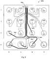
- FIG. 4illustrates a 16-well protein assay microfluidic chip 400 in accordance with the present invention.
- the wells or reservoirs 406 , 408 , 416 – 436 , 440 , 450 , 452 , 484are in fluid communication with the network of microchannels, which includes microchannels 460 – 470 .
- the network of microchannelswhich includes microchannels 460 – 470 .
- ten 416 – 436contain samples to be analyzed
- two 408 484are waste wells
- one 440supplies a reagent such as a fluorescent dye that enables detection of selected species
- one 406is a source of buffer.
- These fourteen wellsare fluidly connected by a first network of channels.
- the remaining two wells 450 , 452are fluidly connected by a second network of channels.
- the first and second networks of channelsare not fluidly connected.
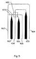
- a region of increased conductivity, a glass resistoris shown generally at a region 490 .
- FIG. 5is a magnified view of the region adjacent the glass resistor 490 which is enclosed by a box for illustrative purposes.
- the basic function of chip 400is to separate a sample into its components by electrophoretic means.
- Means of electrophoretic separationthat may be employed in embodiments of the invention are described in U.S. Pat. No. 5,948,227, which is assigned to the assignee of the present invention.
- the electrophoretic separationtakes place in separation channel 404 .
- Samples from wells 416 – 424are injected into separation channel 404 via channels 462 and 472
- samples from wells 428 – 436are injected into separation channel 404 via channels 464 and 472 .
- the electrophoretic separation of the sampletakes place as the sample travels through the separation channel 404 from the intersection of channels 472 and 404 to waste well 408 .
- a samplecan be preloaded into channel 472 while a previously injected sample is being separated in separation channel 404 .
- the preloading processdoes not interfere with the separation taking place in separation channel 404 because the flow of the sample being preloaded is diverted into channel 460 , which empties into waste well 484 .
- Preloading a subsequent sample in this mannerminimizes the time required to load the sample into the separation channel 404 .
- This type of preloadingis described in more detail in U.S. Pat. No. 5,948,227, and is implemented in DNA and RNA assay chips for the Agilent 2100 Bioanalyzer.
- the sampletravels from its well through either channel 462 or 464 into channel 472 .
- the sampleis propelled through those channels by electrokinetic forces generated by voltages applied between electrodes (not shown) immersed in the sixteen reservoirs of the microfluidic device 400 .
- the samplearrives at the “T” intersection between channels 472 and 404 , the sample is directed to travel straight out of channel 472 , across channel 404 , into the opposite wall of channel 404 .
- the electrical current directing the flow of sample into the wallflows through channel 472 , through the glass resistor 490 , and finally through channel 468 .
- the glass resistorallows electrical current to flow from channel 472 into channel 468 , even though channels 472 and 468 are not in fluid communication.
- the desired electrical currentsare supplied via power-supply electrodes immersed in the sixteen reservoirs of the microfluidic device 400 . If, for example, the sample being injected into separation channel 404 originated from reservoir 418 , the desired electric current would be generated by applying appropriate voltages to electrodes in reservoirs 418 , 450 , and 452 . Note that voltages may have to be simultaneously applied to other reservoirs connected to the first channel network to prevent the flow of other samples into channels 462 , 464 and 472 , and to prevent the diversion of sample into waste well 484 .
- a voltagemay have to be applied across the length of separation channel 404 , by means of voltages applied to electrodes in reservoirs 406 and 408 , to prevent net fluid movement along the separation channel during injection.
- Power suppliescapable of supplying the voltages and currents required to implement this and other embodiments of the invention are described in U.S. Pat. No. 5,965,001, which is assigned to the assignee of the present invention.
- the sampleAs the sample is injected from channel 472 toward the opposing wall of the “T” intersection between channels 472 and 404 , the sample accumulates in the portion of channel 404 near the intersection, providing a more concentrated sample. The longer the sample is concentrated in this manner, the more sample will be available for separation and detection.
- the degree of concentration appropriate for a given analysiswill represent a simple trade-off between loading time and sensitivity.
- a “high sensitivity” scriptcan be run on the same chip as a “normal” script, the only difference being a longer loading time and therefore total analysis time.
- the technique described hereincan be used in connection with the inventions disclosed in Caliper U.S. Pat. Nos. 5,976,336 and 6,153,073, both of which are assigned to the assignee of the present invention.
- the increased conductivity of region 490allows an electrical potential to be maintained across the blind “T” intersection, enabling the flow of fluid from channel 472 to be directed into a wall.
- the increase in conductivitycan be set based on the separation between the channels between which the glass resistor provides a conductive path, and the level of ion implantation in the glass resistor.
- the amount ion implantationcan be determined by the dose amount, the energy level used during implantation, and the thermal annealing process.
- the sheet conductivity of a glass substrate, as measured by a four point probeis about 10 15 ohms per square ( ⁇ / ⁇ ). Ion implantation can increase the glass conductivity by several orders of magnitude, for example up to about 10 8 ⁇ / ⁇ .
- a microfluidic device similar to that shown in FIGS. 4 and 5 with 40 ⁇ m wide channels and with a gap of 100 ⁇ m between channel 490 and channels 466 and 468can be manufactured using the methods described above.
- the glass resistor electrically connecting channel 490 and channel 466 and 468could have a length to width ratio of about 2 (allowing for some lateral current spreading). Assuming a sheet resistance of 10 8 ⁇ / ⁇ , the resistance of the glass resistor would be 2 ⁇ 10 8 ohms. If the current used to inject the sample were about 3 ⁇ A, which is typical of microfluidic devices in accordance with the invention, the voltage drop across the glass resistor would be 600V.
- microfluidic devicesin accordance with the present invention. Such methods include, but are not limited to separating macromolecules by capillary electrophoresis and detecting reactions. Such methods employ a microfluidic device comprising an insulating substrate, at least one of a microchannel and a well formed in the insulating substrate, and at least one ion implanted region in the insulating substrate located at or adjacent the at least one of the microchannel and the well, the at least one ion implanted region having increased conductivity compared to the insulating substrate.
- a method of separating macromolecules by capillary electrophoresiscomprises: providing a microfluidic device, as described above; introducing a sample containing the macromolecules into one end of the microchannel; and applying a voltage gradient across the length of the microchannel, whereby the macromolecules in the sample are separated in the microchannel.
- a method of detecting a reactioncomprises the steps of: introducing a first reagent into a microchannel of the microfluidic device; introducing a second reagent into the microchannel, whereby the first and second reagents mix together to form a reagent mixture; introducing a test compound into the reagent mixture; and detecting an effect of the compound on the reagent mixture.
Landscapes
- Health & Medical Sciences (AREA)
- Chemical & Material Sciences (AREA)
- Engineering & Computer Science (AREA)
- Life Sciences & Earth Sciences (AREA)
- Molecular Biology (AREA)
- Microelectronics & Electronic Packaging (AREA)
- Analytical Chemistry (AREA)
- General Health & Medical Sciences (AREA)
- Chemical Kinetics & Catalysis (AREA)
- Electrochemistry (AREA)
- Clinical Laboratory Science (AREA)
- Physics & Mathematics (AREA)
- Biochemistry (AREA)
- General Physics & Mathematics (AREA)
- Immunology (AREA)
- Pathology (AREA)
- Hematology (AREA)
- Computer Hardware Design (AREA)
- Dispersion Chemistry (AREA)
- Manufacturing & Machinery (AREA)
- Physical Or Chemical Processes And Apparatus (AREA)
- Micromachines (AREA)
Abstract
Description
Claims (12)
Priority Applications (3)
| Application Number | Priority Date | Filing Date | Title |
|---|---|---|---|
| US10/384,349US7195986B1 (en) | 2002-03-08 | 2003-03-07 | Microfluidic device with controlled substrate conductivity |
| US11/595,270US20070053799A1 (en) | 2002-03-08 | 2006-11-10 | Microfluidic device with controlled substrate conductivity |
| US11/707,576US7790116B2 (en) | 2002-03-08 | 2007-02-15 | Microfluidic device with controlled substrate conductivity |
Applications Claiming Priority (2)
| Application Number | Priority Date | Filing Date | Title |
|---|---|---|---|
| US36234002P | 2002-03-08 | 2002-03-08 | |
| US10/384,349US7195986B1 (en) | 2002-03-08 | 2003-03-07 | Microfluidic device with controlled substrate conductivity |
Related Child Applications (2)
| Application Number | Title | Priority Date | Filing Date |
|---|---|---|---|
| US11/595,270ContinuationUS20070053799A1 (en) | 2002-03-08 | 2006-11-10 | Microfluidic device with controlled substrate conductivity |
| US11/707,576DivisionUS7790116B2 (en) | 2002-03-08 | 2007-02-15 | Microfluidic device with controlled substrate conductivity |
Publications (1)
| Publication Number | Publication Date |
|---|---|
| US7195986B1true US7195986B1 (en) | 2007-03-27 |
Family
ID=37886038
Family Applications (3)
| Application Number | Title | Priority Date | Filing Date |
|---|---|---|---|
| US10/384,349Expired - LifetimeUS7195986B1 (en) | 2002-03-08 | 2003-03-07 | Microfluidic device with controlled substrate conductivity |
| US11/595,270AbandonedUS20070053799A1 (en) | 2002-03-08 | 2006-11-10 | Microfluidic device with controlled substrate conductivity |
| US11/707,576Expired - LifetimeUS7790116B2 (en) | 2002-03-08 | 2007-02-15 | Microfluidic device with controlled substrate conductivity |
Family Applications After (2)
| Application Number | Title | Priority Date | Filing Date |
|---|---|---|---|
| US11/595,270AbandonedUS20070053799A1 (en) | 2002-03-08 | 2006-11-10 | Microfluidic device with controlled substrate conductivity |
| US11/707,576Expired - LifetimeUS7790116B2 (en) | 2002-03-08 | 2007-02-15 | Microfluidic device with controlled substrate conductivity |
Country Status (1)
| Country | Link |
|---|---|
| US (3) | US7195986B1 (en) |
Cited By (46)
| Publication number | Priority date | Publication date | Assignee | Title |
|---|---|---|---|---|
| US20090155123A1 (en)* | 2007-07-13 | 2009-06-18 | Handylab, Inc. | Automated Pipetting Apparatus Having a Combined Liquid Pump and Pipette Head System |
| WO2010040354A1 (en)* | 2008-10-08 | 2010-04-15 | Diramo A/S | A method of forming a flow restriction in a fluid communication system |
| US20110207140A1 (en)* | 2006-03-24 | 2011-08-25 | Kalyan Handique | Microfluidic system for amplifying and detecting polynucleotides in parallel |
| US8133671B2 (en) | 2007-07-13 | 2012-03-13 | Handylab, Inc. | Integrated apparatus for performing nucleic acid extraction and diagnostic testing on multiple biological samples |
| US8182763B2 (en) | 2007-07-13 | 2012-05-22 | Handylab, Inc. | Rack for sample tubes and reagent holders |
| US8216530B2 (en) | 2007-07-13 | 2012-07-10 | Handylab, Inc. | Reagent tube |
| USD665095S1 (en) | 2008-07-11 | 2012-08-07 | Handylab, Inc. | Reagent holder |
| USD669191S1 (en) | 2008-07-14 | 2012-10-16 | Handylab, Inc. | Microfluidic cartridge |
| US8324372B2 (en) | 2007-07-13 | 2012-12-04 | Handylab, Inc. | Polynucleotide capture materials, and methods of using same |
| US8415103B2 (en) | 2007-07-13 | 2013-04-09 | Handylab, Inc. | Microfluidic cartridge |
| US8420015B2 (en) | 2001-03-28 | 2013-04-16 | Handylab, Inc. | Systems and methods for thermal actuation of microfluidic devices |
| US8470586B2 (en) | 2004-05-03 | 2013-06-25 | Handylab, Inc. | Processing polynucleotide-containing samples |
| USD692162S1 (en) | 2011-09-30 | 2013-10-22 | Becton, Dickinson And Company | Single piece reagent holder |
| US8617905B2 (en) | 1995-09-15 | 2013-12-31 | The Regents Of The University Of Michigan | Thermal microvalves |
| US8679831B2 (en) | 2003-07-31 | 2014-03-25 | Handylab, Inc. | Processing particle-containing samples |
| US8703069B2 (en) | 2001-03-28 | 2014-04-22 | Handylab, Inc. | Moving microdroplets in a microfluidic device |
| US8709787B2 (en) | 2006-11-14 | 2014-04-29 | Handylab, Inc. | Microfluidic cartridge and method of using same |
| WO2014068408A2 (en) | 2012-10-23 | 2014-05-08 | Caris Life Sciences Switzerland Holdings, S.A.R.L. | Aptamers and uses thereof |
| EP2730662A1 (en) | 2008-11-12 | 2014-05-14 | Caris Life Sciences Luxembourg Holdings | Methods and systems of using exosomes for determining phenotypes |
| WO2014100434A1 (en) | 2012-12-19 | 2014-06-26 | Caris Science, Inc. | Compositions and methods for aptamer screening |
| US8790916B2 (en) | 2009-05-14 | 2014-07-29 | Genestream, Inc. | Microfluidic method and system for isolating particles from biological fluid |
| US8852862B2 (en) | 2004-05-03 | 2014-10-07 | Handylab, Inc. | Method for processing polynucleotide-containing samples |
| US8883490B2 (en) | 2006-03-24 | 2014-11-11 | Handylab, Inc. | Fluorescence detector for microfluidic diagnostic system |
| WO2015031694A2 (en) | 2013-08-28 | 2015-03-05 | Caris Science, Inc. | Oligonucleotide probes and uses thereof |
| US9040288B2 (en) | 2006-03-24 | 2015-05-26 | Handylab, Inc. | Integrated system for processing microfluidic samples, and method of using the same |
| US9051604B2 (en) | 2001-02-14 | 2015-06-09 | Handylab, Inc. | Heat-reduction methods and systems related to microfluidic devices |
| US9128101B2 (en) | 2010-03-01 | 2015-09-08 | Caris Life Sciences Switzerland Holdings Gmbh | Biomarkers for theranostics |
| US9186677B2 (en) | 2007-07-13 | 2015-11-17 | Handylab, Inc. | Integrated apparatus for performing nucleic acid extraction and diagnostic testing on multiple biological samples |
| US9222954B2 (en) | 2011-09-30 | 2015-12-29 | Becton, Dickinson And Company | Unitized reagent strip |
| WO2016145128A1 (en) | 2015-03-09 | 2016-09-15 | Caris Science, Inc. | Oligonucleotide probes and uses thereof |
| US9469876B2 (en) | 2010-04-06 | 2016-10-18 | Caris Life Sciences Switzerland Holdings Gmbh | Circulating biomarkers for metastatic prostate cancer |
| WO2017004243A1 (en) | 2015-06-29 | 2017-01-05 | Caris Science, Inc. | Therapeutic oligonucleotides |
| WO2017019918A1 (en) | 2015-07-28 | 2017-02-02 | Caris Science, Inc. | Targeted oligonucleotides |
| US9618139B2 (en) | 2007-07-13 | 2017-04-11 | Handylab, Inc. | Integrated heater and magnetic separator |
| USD787087S1 (en) | 2008-07-14 | 2017-05-16 | Handylab, Inc. | Housing |
| US9765389B2 (en) | 2011-04-15 | 2017-09-19 | Becton, Dickinson And Company | Scanning real-time microfluidic thermocycler and methods for synchronized thermocycling and scanning optical detection |
| WO2017205686A1 (en) | 2016-05-25 | 2017-11-30 | Caris Science, Inc. | Oligonucleotide probes and uses thereof |
| WO2020113237A1 (en) | 2018-11-30 | 2020-06-04 | Caris Mpi, Inc. | Next-generation molecular profiling |
| US10731166B2 (en) | 2016-03-18 | 2020-08-04 | Caris Science, Inc. | Oligonucleotide probes and uses thereof |
| US10822644B2 (en) | 2012-02-03 | 2020-11-03 | Becton, Dickinson And Company | External files for distribution of molecular diagnostic tests and determination of compatibility between tests |
| US10900066B2 (en) | 2006-03-24 | 2021-01-26 | Handylab, Inc. | Microfluidic system for amplifying and detecting polynucleotides in parallel |
| US10942184B2 (en) | 2012-10-23 | 2021-03-09 | Caris Science, Inc. | Aptamers and uses thereof |
| US11123735B2 (en) | 2019-10-10 | 2021-09-21 | 1859, Inc. | Methods and systems for microfluidic screening |
| US11453906B2 (en) | 2011-11-04 | 2022-09-27 | Handylab, Inc. | Multiplexed diagnostic detection apparatus and methods |
| US11806718B2 (en) | 2006-03-24 | 2023-11-07 | Handylab, Inc. | Fluorescence detector for microfluidic diagnostic system |
| US11842805B2 (en) | 2019-12-02 | 2023-12-12 | Caris Mpi, Inc. | Pan-cancer platinum response predictor |
Families Citing this family (7)
| Publication number | Priority date | Publication date | Assignee | Title |
|---|---|---|---|---|
| AU2001269929B2 (en)* | 2000-06-19 | 2005-11-03 | Caliper Life Sciences, Inc. | Methods and devices for enhancing bonded substrate yields and regulating temperature |
| KR100811267B1 (en)* | 2005-12-22 | 2008-03-07 | 주식회사 하이닉스반도체 | Method of fabricating the dual gate in semiconductor device |
| US8016260B2 (en)* | 2007-07-19 | 2011-09-13 | Formulatrix, Inc. | Metering assembly and method of dispensing fluid |
| EP2331251A4 (en)* | 2008-08-13 | 2017-03-08 | Advanced Liquid Logic, Inc. | Methods, systems, and products for conducting droplet operations |
| JP5609648B2 (en)* | 2008-11-26 | 2014-10-22 | 住友ベークライト株式会社 | Microchannel device |
| US8100293B2 (en)* | 2009-01-23 | 2012-01-24 | Formulatrix, Inc. | Microfluidic dispensing assembly |
| US20110312078A1 (en)* | 2010-06-17 | 2011-12-22 | Geneasys Pty Ltd | Microfluidic device for detecting target nucleic acid sequences in mitochondrial dna |
Citations (10)
| Publication number | Priority date | Publication date | Assignee | Title |
|---|---|---|---|---|
| US5779868A (en) | 1996-06-28 | 1998-07-14 | Caliper Technologies Corporation | Electropipettor and compensation means for electrophoretic bias |
| US5858195A (en) | 1994-08-01 | 1999-01-12 | Lockheed Martin Energy Research Corporation | Apparatus and method for performing microfluidic manipulations for chemical analysis and synthesis |
| US5948227A (en) | 1997-12-17 | 1999-09-07 | Caliper Technologies Corp. | Methods and systems for performing electrophoretic molecular separations |
| US5965001A (en) | 1996-07-03 | 1999-10-12 | Caliper Technologies Corporation | Variable control of electroosmotic and/or electrophoretic forces within a fluid-containing structure via electrical forces |
| US5965410A (en) | 1997-09-02 | 1999-10-12 | Caliper Technologies Corp. | Electrical current for controlling fluid parameters in microchannels |
| US5976336A (en) | 1997-04-25 | 1999-11-02 | Caliper Technologies Corp. | Microfluidic devices incorporating improved channel geometries |
| US6090251A (en) | 1997-06-06 | 2000-07-18 | Caliper Technologies, Inc. | Microfabricated structures for facilitating fluid introduction into microfluidic devices |
| US6153073A (en) | 1997-04-25 | 2000-11-28 | Caliper Technologies Corp. | Microfluidic devices incorporating improved channel geometries |
| US6271021B1 (en)* | 1995-09-15 | 2001-08-07 | The Regents Of The University Of Michigan | Microscale devices and reactions in microscale devices |
| US20040201013A1 (en)* | 2001-09-12 | 2004-10-14 | Faris Sadeg M. | Method of fabricating multi layer mems and microfluidic devices |
Family Cites Families (3)
| Publication number | Priority date | Publication date | Assignee | Title |
|---|---|---|---|---|
| WO1998022625A1 (en)* | 1996-11-20 | 1998-05-28 | The Regents Of The University Of Michigan | Microfabricated isothermal nucleic acid amplification devices and methods |
| US6197557B1 (en)* | 1997-03-05 | 2001-03-06 | The Regents Of The University Of Michigan | Compositions and methods for analysis of nucleic acids |
| US6582987B2 (en)* | 2000-12-30 | 2003-06-24 | Electronics And Telecommunications Research Institute | Method of fabricating microchannel array structure embedded in silicon substrate |
- 2003
- 2003-03-07USUS10/384,349patent/US7195986B1/ennot_activeExpired - Lifetime
- 2006
- 2006-11-10USUS11/595,270patent/US20070053799A1/ennot_activeAbandoned
- 2007
- 2007-02-15USUS11/707,576patent/US7790116B2/ennot_activeExpired - Lifetime
Patent Citations (11)
| Publication number | Priority date | Publication date | Assignee | Title |
|---|---|---|---|---|
| US5858195A (en) | 1994-08-01 | 1999-01-12 | Lockheed Martin Energy Research Corporation | Apparatus and method for performing microfluidic manipulations for chemical analysis and synthesis |
| US6001229A (en) | 1994-08-01 | 1999-12-14 | Lockheed Martin Energy Systems, Inc. | Apparatus and method for performing microfluidic manipulations for chemical analysis |
| US6271021B1 (en)* | 1995-09-15 | 2001-08-07 | The Regents Of The University Of Michigan | Microscale devices and reactions in microscale devices |
| US5779868A (en) | 1996-06-28 | 1998-07-14 | Caliper Technologies Corporation | Electropipettor and compensation means for electrophoretic bias |
| US5965001A (en) | 1996-07-03 | 1999-10-12 | Caliper Technologies Corporation | Variable control of electroosmotic and/or electrophoretic forces within a fluid-containing structure via electrical forces |
| US5976336A (en) | 1997-04-25 | 1999-11-02 | Caliper Technologies Corp. | Microfluidic devices incorporating improved channel geometries |
| US6153073A (en) | 1997-04-25 | 2000-11-28 | Caliper Technologies Corp. | Microfluidic devices incorporating improved channel geometries |
| US6090251A (en) | 1997-06-06 | 2000-07-18 | Caliper Technologies, Inc. | Microfabricated structures for facilitating fluid introduction into microfluidic devices |
| US5965410A (en) | 1997-09-02 | 1999-10-12 | Caliper Technologies Corp. | Electrical current for controlling fluid parameters in microchannels |
| US5948227A (en) | 1997-12-17 | 1999-09-07 | Caliper Technologies Corp. | Methods and systems for performing electrophoretic molecular separations |
| US20040201013A1 (en)* | 2001-09-12 | 2004-10-14 | Faris Sadeg M. | Method of fabricating multi layer mems and microfluidic devices |
Non-Patent Citations (8)
Cited By (139)
| Publication number | Priority date | Publication date | Assignee | Title |
|---|---|---|---|---|
| US8617905B2 (en) | 1995-09-15 | 2013-12-31 | The Regents Of The University Of Michigan | Thermal microvalves |
| US9051604B2 (en) | 2001-02-14 | 2015-06-09 | Handylab, Inc. | Heat-reduction methods and systems related to microfluidic devices |
| US9528142B2 (en) | 2001-02-14 | 2016-12-27 | Handylab, Inc. | Heat-reduction methods and systems related to microfluidic devices |
| US10351901B2 (en) | 2001-03-28 | 2019-07-16 | Handylab, Inc. | Systems and methods for thermal actuation of microfluidic devices |
| US8894947B2 (en) | 2001-03-28 | 2014-11-25 | Handylab, Inc. | Systems and methods for thermal actuation of microfluidic devices |
| US8703069B2 (en) | 2001-03-28 | 2014-04-22 | Handylab, Inc. | Moving microdroplets in a microfluidic device |
| US10619191B2 (en) | 2001-03-28 | 2020-04-14 | Handylab, Inc. | Systems and methods for thermal actuation of microfluidic devices |
| US8420015B2 (en) | 2001-03-28 | 2013-04-16 | Handylab, Inc. | Systems and methods for thermal actuation of microfluidic devices |
| US9677121B2 (en) | 2001-03-28 | 2017-06-13 | Handylab, Inc. | Systems and methods for thermal actuation of microfluidic devices |
| US9670528B2 (en) | 2003-07-31 | 2017-06-06 | Handylab, Inc. | Processing particle-containing samples |
| US10731201B2 (en) | 2003-07-31 | 2020-08-04 | Handylab, Inc. | Processing particle-containing samples |
| US8679831B2 (en) | 2003-07-31 | 2014-03-25 | Handylab, Inc. | Processing particle-containing samples |
| US10865437B2 (en) | 2003-07-31 | 2020-12-15 | Handylab, Inc. | Processing particle-containing samples |
| US11078523B2 (en) | 2003-07-31 | 2021-08-03 | Handylab, Inc. | Processing particle-containing samples |
| US12139745B2 (en) | 2003-07-31 | 2024-11-12 | Handylab, Inc. | Processing particle-containing samples |
| US10364456B2 (en) | 2004-05-03 | 2019-07-30 | Handylab, Inc. | Method for processing polynucleotide-containing samples |
| US10443088B1 (en) | 2004-05-03 | 2019-10-15 | Handylab, Inc. | Method for processing polynucleotide-containing samples |
| US10494663B1 (en) | 2004-05-03 | 2019-12-03 | Handylab, Inc. | Method for processing polynucleotide-containing samples |
| US10604788B2 (en) | 2004-05-03 | 2020-03-31 | Handylab, Inc. | System for processing polynucleotide-containing samples |
| US8470586B2 (en) | 2004-05-03 | 2013-06-25 | Handylab, Inc. | Processing polynucleotide-containing samples |
| US8852862B2 (en) | 2004-05-03 | 2014-10-07 | Handylab, Inc. | Method for processing polynucleotide-containing samples |
| US11441171B2 (en) | 2004-05-03 | 2022-09-13 | Handylab, Inc. | Method for processing polynucleotide-containing samples |
| US11085069B2 (en) | 2006-03-24 | 2021-08-10 | Handylab, Inc. | Microfluidic system for amplifying and detecting polynucleotides in parallel |
| US20110207140A1 (en)* | 2006-03-24 | 2011-08-25 | Kalyan Handique | Microfluidic system for amplifying and detecting polynucleotides in parallel |
| US8323900B2 (en) | 2006-03-24 | 2012-12-04 | Handylab, Inc. | Microfluidic system for amplifying and detecting polynucleotides in parallel |
| US12162007B2 (en) | 2006-03-24 | 2024-12-10 | Handylab, Inc. | Integrated system for processing microfluidic samples, and method of using same |
| US10695764B2 (en) | 2006-03-24 | 2020-06-30 | Handylab, Inc. | Fluorescence detector for microfluidic diagnostic system |
| US8883490B2 (en) | 2006-03-24 | 2014-11-11 | Handylab, Inc. | Fluorescence detector for microfluidic diagnostic system |
| US10799862B2 (en) | 2006-03-24 | 2020-10-13 | Handylab, Inc. | Integrated system for processing microfluidic samples, and method of using same |
| US11959126B2 (en) | 2006-03-24 | 2024-04-16 | Handylab, Inc. | Microfluidic system for amplifying and detecting polynucleotides in parallel |
| US11806718B2 (en) | 2006-03-24 | 2023-11-07 | Handylab, Inc. | Fluorescence detector for microfluidic diagnostic system |
| US9040288B2 (en) | 2006-03-24 | 2015-05-26 | Handylab, Inc. | Integrated system for processing microfluidic samples, and method of using the same |
| US10821436B2 (en) | 2006-03-24 | 2020-11-03 | Handylab, Inc. | Integrated system for processing microfluidic samples, and method of using the same |
| US9080207B2 (en) | 2006-03-24 | 2015-07-14 | Handylab, Inc. | Microfluidic system for amplifying and detecting polynucleotides in parallel |
| US11666903B2 (en) | 2006-03-24 | 2023-06-06 | Handylab, Inc. | Integrated system for processing microfluidic samples, and method of using same |
| US9802199B2 (en) | 2006-03-24 | 2017-10-31 | Handylab, Inc. | Fluorescence detector for microfluidic diagnostic system |
| US11141734B2 (en) | 2006-03-24 | 2021-10-12 | Handylab, Inc. | Fluorescence detector for microfluidic diagnostic system |
| US11142785B2 (en) | 2006-03-24 | 2021-10-12 | Handylab, Inc. | Microfluidic system for amplifying and detecting polynucleotides in parallel |
| US10913061B2 (en) | 2006-03-24 | 2021-02-09 | Handylab, Inc. | Integrated system for processing microfluidic samples, and method of using the same |
| US10900066B2 (en) | 2006-03-24 | 2021-01-26 | Handylab, Inc. | Microfluidic system for amplifying and detecting polynucleotides in parallel |
| US10857535B2 (en) | 2006-03-24 | 2020-12-08 | Handylab, Inc. | Integrated system for processing microfluidic samples, and method of using same |
| US10843188B2 (en) | 2006-03-24 | 2020-11-24 | Handylab, Inc. | Integrated system for processing microfluidic samples, and method of using the same |
| US10821446B1 (en) | 2006-03-24 | 2020-11-03 | Handylab, Inc. | Fluorescence detector for microfluidic diagnostic system |
| US8709787B2 (en) | 2006-11-14 | 2014-04-29 | Handylab, Inc. | Microfluidic cartridge and method of using same |
| US12030050B2 (en) | 2006-11-14 | 2024-07-09 | Handylab, Inc. | Microfluidic cartridge and method of making same |
| US10710069B2 (en) | 2006-11-14 | 2020-07-14 | Handylab, Inc. | Microfluidic valve and method of making same |
| US12128405B2 (en) | 2006-11-14 | 2024-10-29 | Handylab, Inc. | Microfluidic valve and method of making same |
| US8765076B2 (en) | 2006-11-14 | 2014-07-01 | Handylab, Inc. | Microfluidic valve and method of making same |
| US9815057B2 (en) | 2006-11-14 | 2017-11-14 | Handylab, Inc. | Microfluidic cartridge and method of making same |
| US9701957B2 (en) | 2007-07-13 | 2017-07-11 | Handylab, Inc. | Reagent holder, and kits containing same |
| US8324372B2 (en) | 2007-07-13 | 2012-12-04 | Handylab, Inc. | Polynucleotide capture materials, and methods of using same |
| US8415103B2 (en) | 2007-07-13 | 2013-04-09 | Handylab, Inc. | Microfluidic cartridge |
| US12397295B2 (en) | 2007-07-13 | 2025-08-26 | Handylab, Inc. | Integrated apparatus for performing nucleic acid extraction and diagnostic testing on multiple biological samples |
| US12128402B2 (en) | 2007-07-13 | 2024-10-29 | Handylab, Inc. | Microfluidic cartridge |
| US11845081B2 (en) | 2007-07-13 | 2023-12-19 | Handylab, Inc. | Integrated apparatus for performing nucleic acid extraction and diagnostic testing on multiple biological samples |
| US11549959B2 (en) | 2007-07-13 | 2023-01-10 | Handylab, Inc. | Automated pipetting apparatus having a combined liquid pump and pipette head system |
| US9618139B2 (en) | 2007-07-13 | 2017-04-11 | Handylab, Inc. | Integrated heater and magnetic separator |
| US11466263B2 (en) | 2007-07-13 | 2022-10-11 | Handylab, Inc. | Diagnostic apparatus to extract nucleic acids including a magnetic assembly and a heater assembly |
| US11266987B2 (en) | 2007-07-13 | 2022-03-08 | Handylab, Inc. | Microfluidic cartridge |
| US11254927B2 (en) | 2007-07-13 | 2022-02-22 | Handylab, Inc. | Polynucleotide capture materials, and systems using same |
| US10065185B2 (en) | 2007-07-13 | 2018-09-04 | Handylab, Inc. | Microfluidic cartridge |
| US10071376B2 (en) | 2007-07-13 | 2018-09-11 | Handylab, Inc. | Integrated apparatus for performing nucleic acid extraction and diagnostic testing on multiple biological samples |
| US9186677B2 (en) | 2007-07-13 | 2015-11-17 | Handylab, Inc. | Integrated apparatus for performing nucleic acid extraction and diagnostic testing on multiple biological samples |
| US10100302B2 (en) | 2007-07-13 | 2018-10-16 | Handylab, Inc. | Polynucleotide capture materials, and methods of using same |
| US9217143B2 (en) | 2007-07-13 | 2015-12-22 | Handylab, Inc. | Polynucleotide capture materials, and methods of using same |
| US10139012B2 (en) | 2007-07-13 | 2018-11-27 | Handylab, Inc. | Integrated heater and magnetic separator |
| US10179910B2 (en) | 2007-07-13 | 2019-01-15 | Handylab, Inc. | Rack for sample tubes and reagent holders |
| US10234474B2 (en) | 2007-07-13 | 2019-03-19 | Handylab, Inc. | Automated pipetting apparatus having a combined liquid pump and pipette head system |
| US9347586B2 (en) | 2007-07-13 | 2016-05-24 | Handylab, Inc. | Automated pipetting apparatus having a combined liquid pump and pipette head system |
| US20090155123A1 (en)* | 2007-07-13 | 2009-06-18 | Handylab, Inc. | Automated Pipetting Apparatus Having a Combined Liquid Pump and Pipette Head System |
| US8287820B2 (en) | 2007-07-13 | 2012-10-16 | Handylab, Inc. | Automated pipetting apparatus having a combined liquid pump and pipette head system |
| US11060082B2 (en) | 2007-07-13 | 2021-07-13 | Handy Lab, Inc. | Polynucleotide capture materials, and systems using same |
| US9238223B2 (en) | 2007-07-13 | 2016-01-19 | Handylab, Inc. | Microfluidic cartridge |
| US10590410B2 (en) | 2007-07-13 | 2020-03-17 | Handylab, Inc. | Polynucleotide capture materials, and methods of using same |
| US10844368B2 (en) | 2007-07-13 | 2020-11-24 | Handylab, Inc. | Diagnostic apparatus to extract nucleic acids including a magnetic assembly and a heater assembly |
| US8216530B2 (en) | 2007-07-13 | 2012-07-10 | Handylab, Inc. | Reagent tube |
| US10625262B2 (en) | 2007-07-13 | 2020-04-21 | Handylab, Inc. | Integrated apparatus for performing nucleic acid extraction and diagnostic testing on multiple biological samples |
| US10625261B2 (en) | 2007-07-13 | 2020-04-21 | Handylab, Inc. | Integrated apparatus for performing nucleic acid extraction and diagnostic testing on multiple biological samples |
| US10632466B1 (en) | 2007-07-13 | 2020-04-28 | Handylab, Inc. | Integrated apparatus for performing nucleic acid extraction and diagnostic testing on multiple biological samples |
| US10875022B2 (en) | 2007-07-13 | 2020-12-29 | Handylab, Inc. | Integrated apparatus for performing nucleic acid extraction and diagnostic testing on multiple biological samples |
| US8133671B2 (en) | 2007-07-13 | 2012-03-13 | Handylab, Inc. | Integrated apparatus for performing nucleic acid extraction and diagnostic testing on multiple biological samples |
| US8710211B2 (en) | 2007-07-13 | 2014-04-29 | Handylab, Inc. | Polynucleotide capture materials, and methods of using same |
| US10717085B2 (en) | 2007-07-13 | 2020-07-21 | Handylab, Inc. | Integrated apparatus for performing nucleic acid extraction and diagnostic testing on multiple biological samples |
| US9259734B2 (en) | 2007-07-13 | 2016-02-16 | Handylab, Inc. | Integrated apparatus for performing nucleic acid extraction and diagnostic testing on multiple biological samples |
| US8182763B2 (en) | 2007-07-13 | 2012-05-22 | Handylab, Inc. | Rack for sample tubes and reagent holders |
| USD665095S1 (en) | 2008-07-11 | 2012-08-07 | Handylab, Inc. | Reagent holder |
| USD669191S1 (en) | 2008-07-14 | 2012-10-16 | Handylab, Inc. | Microfluidic cartridge |
| USD787087S1 (en) | 2008-07-14 | 2017-05-16 | Handylab, Inc. | Housing |
| US20110232090A1 (en)* | 2008-10-08 | 2011-09-29 | Flowsion Aps | Method of forming a flow restriction in a fluid communication system |
| US9015945B2 (en) | 2008-10-08 | 2015-04-28 | Flowsion Aps | Method of forming a flow restriction in a fluid communication system |
| WO2010040354A1 (en)* | 2008-10-08 | 2010-04-15 | Diramo A/S | A method of forming a flow restriction in a fluid communication system |
| EP2730662A1 (en) | 2008-11-12 | 2014-05-14 | Caris Life Sciences Luxembourg Holdings | Methods and systems of using exosomes for determining phenotypes |
| EP3181705A1 (en) | 2008-11-12 | 2017-06-21 | Caris Life Sciences Switzerland Holdings GmbH | Methods and systems of using exosomes for determining phenotypes |
| US8790916B2 (en) | 2009-05-14 | 2014-07-29 | Genestream, Inc. | Microfluidic method and system for isolating particles from biological fluid |
| US9128101B2 (en) | 2010-03-01 | 2015-09-08 | Caris Life Sciences Switzerland Holdings Gmbh | Biomarkers for theranostics |
| US9469876B2 (en) | 2010-04-06 | 2016-10-18 | Caris Life Sciences Switzerland Holdings Gmbh | Circulating biomarkers for metastatic prostate cancer |
| US9765389B2 (en) | 2011-04-15 | 2017-09-19 | Becton, Dickinson And Company | Scanning real-time microfluidic thermocycler and methods for synchronized thermocycling and scanning optical detection |
| US11788127B2 (en) | 2011-04-15 | 2023-10-17 | Becton, Dickinson And Company | Scanning real-time microfluidic thermocycler and methods for synchronized thermocycling and scanning optical detection |
| US10781482B2 (en) | 2011-04-15 | 2020-09-22 | Becton, Dickinson And Company | Scanning real-time microfluidic thermocycler and methods for synchronized thermocycling and scanning optical detection |
| US10076754B2 (en) | 2011-09-30 | 2018-09-18 | Becton, Dickinson And Company | Unitized reagent strip |
| USD831843S1 (en) | 2011-09-30 | 2018-10-23 | Becton, Dickinson And Company | Single piece reagent holder |
| USD692162S1 (en) | 2011-09-30 | 2013-10-22 | Becton, Dickinson And Company | Single piece reagent holder |
| USD905269S1 (en) | 2011-09-30 | 2020-12-15 | Becton, Dickinson And Company | Single piece reagent holder |
| USD1029291S1 (en) | 2011-09-30 | 2024-05-28 | Becton, Dickinson And Company | Single piece reagent holder |
| USD742027S1 (en) | 2011-09-30 | 2015-10-27 | Becton, Dickinson And Company | Single piece reagent holder |
| US9222954B2 (en) | 2011-09-30 | 2015-12-29 | Becton, Dickinson And Company | Unitized reagent strip |
| US9480983B2 (en) | 2011-09-30 | 2016-11-01 | Becton, Dickinson And Company | Unitized reagent strip |
| US11453906B2 (en) | 2011-11-04 | 2022-09-27 | Handylab, Inc. | Multiplexed diagnostic detection apparatus and methods |
| US10822644B2 (en) | 2012-02-03 | 2020-11-03 | Becton, Dickinson And Company | External files for distribution of molecular diagnostic tests and determination of compatibility between tests |
| WO2014068408A2 (en) | 2012-10-23 | 2014-05-08 | Caris Life Sciences Switzerland Holdings, S.A.R.L. | Aptamers and uses thereof |
| US9958448B2 (en) | 2012-10-23 | 2018-05-01 | Caris Life Sciences Switzerland Holdings Gmbh | Aptamers and uses thereof |
| EP4170031A1 (en) | 2012-10-23 | 2023-04-26 | Caris Science, Inc. | Aptamers and uses thereof |
| US10942184B2 (en) | 2012-10-23 | 2021-03-09 | Caris Science, Inc. | Aptamers and uses thereof |
| WO2014100434A1 (en) | 2012-12-19 | 2014-06-26 | Caris Science, Inc. | Compositions and methods for aptamer screening |
| US9939443B2 (en) | 2012-12-19 | 2018-04-10 | Caris Life Sciences Switzerland Holdings Gmbh | Compositions and methods for aptamer screening |
| WO2015031694A2 (en) | 2013-08-28 | 2015-03-05 | Caris Science, Inc. | Oligonucleotide probes and uses thereof |
| WO2016145128A1 (en) | 2015-03-09 | 2016-09-15 | Caris Science, Inc. | Oligonucleotide probes and uses thereof |
| US10590425B2 (en) | 2015-06-29 | 2020-03-17 | Caris Science, Inc. | Therapeutic oligonucleotides |
| US11091765B2 (en) | 2015-06-29 | 2021-08-17 | Caris Science, Inc. | Therapeutic oligonucleotides |
| WO2017004243A1 (en) | 2015-06-29 | 2017-01-05 | Caris Science, Inc. | Therapeutic oligonucleotides |
| US11725023B2 (en) | 2015-07-28 | 2023-08-15 | Caris Science, Inc. | Therapeutic oligonucleotides |
| US10941176B2 (en) | 2015-07-28 | 2021-03-09 | Caris Science, Inc. | Therapeutic oligonucleotides |
| WO2017019918A1 (en) | 2015-07-28 | 2017-02-02 | Caris Science, Inc. | Targeted oligonucleotides |
| US10731166B2 (en) | 2016-03-18 | 2020-08-04 | Caris Science, Inc. | Oligonucleotide probes and uses thereof |
| US11332748B2 (en) | 2016-03-18 | 2022-05-17 | Caris Science, Inc. | Oligonucleotide probes and uses thereof |
| EP3828272A1 (en) | 2016-03-18 | 2021-06-02 | Caris Science, Inc. | Oligonucleotide probes and uses thereof |
| EP4339288A2 (en) | 2016-03-18 | 2024-03-20 | Caris Science, Inc. | Oligonucleotide probes and uses thereof |
| US11293017B2 (en) | 2016-05-25 | 2022-04-05 | Caris Science, Inc. | Oligonucleotide probes and uses thereof |
| WO2017205686A1 (en) | 2016-05-25 | 2017-11-30 | Caris Science, Inc. | Oligonucleotide probes and uses thereof |
| US11315673B2 (en) | 2018-11-30 | 2022-04-26 | Caris Mpi, Inc. | Next-generation molecular profiling |
| EP4369356A2 (en) | 2018-11-30 | 2024-05-15 | Caris MPI, Inc. | Next-generation molecular profiling |
| US12165759B2 (en) | 2018-11-30 | 2024-12-10 | Caris Mpi, Inc. | Classifying an entity for FOLFOX treatment |
| WO2020113237A1 (en) | 2018-11-30 | 2020-06-04 | Caris Mpi, Inc. | Next-generation molecular profiling |
| US11919000B2 (en) | 2019-10-10 | 2024-03-05 | 1859, Inc. | Methods and systems for microfluidic screening |
| US11351544B2 (en) | 2019-10-10 | 2022-06-07 | 1859, Inc. | Methods and systems for microfluidic screening |
| US11351543B2 (en) | 2019-10-10 | 2022-06-07 | 1859, Inc. | Methods and systems for microfluidic screening |
| US11247209B2 (en) | 2019-10-10 | 2022-02-15 | 1859, Inc. | Methods and systems for microfluidic screening |
| US11123735B2 (en) | 2019-10-10 | 2021-09-21 | 1859, Inc. | Methods and systems for microfluidic screening |
| US11842805B2 (en) | 2019-12-02 | 2023-12-12 | Caris Mpi, Inc. | Pan-cancer platinum response predictor |
Also Published As
| Publication number | Publication date |
|---|---|
| US20070053799A1 (en) | 2007-03-08 |
| US20070202015A1 (en) | 2007-08-30 |
| US7790116B2 (en) | 2010-09-07 |
Similar Documents
| Publication | Publication Date | Title |
|---|---|---|
| US7195986B1 (en) | Microfluidic device with controlled substrate conductivity | |
| Soper et al. | Peer Reviewed: Polymeric Microelectromechanical Systems. | |
| EP1511570B1 (en) | Micro fluidic structures | |
| US5900130A (en) | Method for sample injection in microchannel device | |
| US6001229A (en) | Apparatus and method for performing microfluidic manipulations for chemical analysis | |
| US6261430B1 (en) | Micro-electrophoresis chip for moving and separating nucleic acids and other charged molecules | |
| EP0996547B1 (en) | The production of microstructures for use in assays | |
| Coltro et al. | Comparison of the analytical performance of electrophoresis microchannels fabricated in PDMS, glass, and polyester‐toner | |
| CN103620398B (en) | Apparatus and method for applying continuous electric field | |
| Li et al. | PDMS-based microfluidic device with multi-height structures fabricated by single-step photolithography using printed circuit board as masters | |
| Keynton et al. | Design and development of microfabricated capillary electrophoresis devices with electrochemical detection | |
| EP1431018B1 (en) | Method of producing resin molded product | |
| US20110272281A1 (en) | Microfluidic device for separating, fractionating, or preconcentrating analytes contained in an electrolyte | |
| Liu et al. | Side-by-side comparison of disposable microchips with commercial capillary cartridges for application in capillary isoelectric focusing with whole column imaging detection | |
| KR100492284B1 (en) | Method of manufacturing microchip | |
| US11673798B2 (en) | Microfluidic devices with electrodes formed as physically separated sections of microchannel side walls | |
| Yang et al. | Free-flow isoelectric focusing microfluidic device with glass coating by sol–gel methods | |
| Bressan et al. | Microchip electrophoresis containing electrodes for integrated electrochemical detection | |
| Chen et al. | Fabrication of PMMA CE microchips by infrared‐assisted polymerization | |
| CN100561226C (en) | Low-voltage driving array electrode type capillary electrophoresis chip | |
| Liu et al. | Characterization of molecular transport in poly (dimethylsiloxane) microchannels for electrophoresis fabricated with synchrotron radiation-lithography and UV-photolithography | |
| Yan et al. | Fluidic microchannel arrays for the electrophoretic separation and detection of bioanalytes using electrochemiluminescence | |
| Matzke et al. | Quartz channel fabrication for electrokinetically driven separations | |
| Ford | Fabricating microfluidic devices in polymers for bioanalytica applications | |
| KR20050000585A (en) | Method for manufacturing microchip |
Legal Events
| Date | Code | Title | Description |
|---|---|---|---|
| AS | Assignment | Owner name:CALIPER TECHNOLOGIES CORP., CALIFORNIA Free format text:ASSIGNMENT OF ASSIGNORS INTEREST;ASSIGNORS:BOUSSE, LUC J.;STERN, SETH R.;MCREYNOLDS, RICHARD J.;REEL/FRAME:014260/0001 Effective date:20030707 | |
| AS | Assignment | Owner name:CALIPER LIFE SCIENCES, INC., CALIFORNIA Free format text:CHANGE OF NAME;ASSIGNOR:CALIPER TECHNOLOGIES CORP.;REEL/FRAME:014326/0407 Effective date:20040123 Owner name:CALIPER LIFE SCIENCES, INC.,CALIFORNIA Free format text:CHANGE OF NAME;ASSIGNOR:CALIPER TECHNOLOGIES CORP.;REEL/FRAME:014326/0407 Effective date:20040123 | |
| AS | Assignment | Owner name:CALIPER LIFE SCIENCES, INC., CALIFORNIA Free format text:ASSIGNMENT OF ASSIGNORS INTEREST;ASSIGNOR:CALIPER TECHNOLOGIES CORP.;REEL/FRAME:018499/0279 Effective date:20040123 | |
| STCF | Information on status: patent grant | Free format text:PATENTED CASE | |
| FPAY | Fee payment | Year of fee payment:4 | |
| FPAY | Fee payment | Year of fee payment:8 | |
| MAFP | Maintenance fee payment | Free format text:PAYMENT OF MAINTENANCE FEE, 12TH YEAR, LARGE ENTITY (ORIGINAL EVENT CODE: M1553); ENTITY STATUS OF PATENT OWNER: LARGE ENTITY Year of fee payment:12 |