US7193398B2 - Tip having active circuitry - Google Patents
Tip having active circuitryDownload PDFInfo
- Publication number
- US7193398B2 US7193398B2US10/927,619US92761904AUS7193398B2US 7193398 B2US7193398 B2US 7193398B2US 92761904 AUS92761904 AUS 92761904AUS 7193398 B2US7193398 B2US 7193398B2
- Authority
- US
- United States
- Prior art keywords
- tip
- prog
- voltage
- adapter
- error
- Prior art date
- Legal status (The legal status is an assumption and is not a legal conclusion. Google has not performed a legal analysis and makes no representation as to the accuracy of the status listed.)
- Expired - Fee Related
Links
Images


Classifications
- G—PHYSICS
- G05—CONTROLLING; REGULATING
- G05F—SYSTEMS FOR REGULATING ELECTRIC OR MAGNETIC VARIABLES
- G05F1/00—Automatic systems in which deviations of an electric quantity from one or more predetermined values are detected at the output of the system and fed back to a device within the system to restore the detected quantity to its predetermined value or values, i.e. retroactive systems
- G05F1/10—Regulating voltage or current
- G05F1/46—Regulating voltage or current wherein the variable actually regulated by the final control device is DC
- G05F1/56—Regulating voltage or current wherein the variable actually regulated by the final control device is DC using semiconductor devices in series with the load as final control devices
- H—ELECTRICITY
- H02—GENERATION; CONVERSION OR DISTRIBUTION OF ELECTRIC POWER
- H02M—APPARATUS FOR CONVERSION BETWEEN AC AND AC, BETWEEN AC AND DC, OR BETWEEN DC AND DC, AND FOR USE WITH MAINS OR SIMILAR POWER SUPPLY SYSTEMS; CONVERSION OF DC OR AC INPUT POWER INTO SURGE OUTPUT POWER; CONTROL OR REGULATION THEREOF
- H02M1/00—Details of apparatus for conversion
- H02M1/10—Arrangements incorporating converting means for enabling loads to be operated at will from different kinds of power supplies, e.g. from AC or DC
- H—ELECTRICITY
- H02—GENERATION; CONVERSION OR DISTRIBUTION OF ELECTRIC POWER
- H02M—APPARATUS FOR CONVERSION BETWEEN AC AND AC, BETWEEN AC AND DC, OR BETWEEN DC AND DC, AND FOR USE WITH MAINS OR SIMILAR POWER SUPPLY SYSTEMS; CONVERSION OF DC OR AC INPUT POWER INTO SURGE OUTPUT POWER; CONTROL OR REGULATION THEREOF
- H02M1/00—Details of apparatus for conversion
- H02M1/0045—Converters combining the concepts of switch-mode regulation and linear regulation, e.g. linear pre-regulator to switching converter, linear and switching converter in parallel, same converter or same transistor operating either in linear or switching mode
- H—ELECTRICITY
- H02—GENERATION; CONVERSION OR DISTRIBUTION OF ELECTRIC POWER
- H02M—APPARATUS FOR CONVERSION BETWEEN AC AND AC, BETWEEN AC AND DC, OR BETWEEN DC AND DC, AND FOR USE WITH MAINS OR SIMILAR POWER SUPPLY SYSTEMS; CONVERSION OF DC OR AC INPUT POWER INTO SURGE OUTPUT POWER; CONTROL OR REGULATION THEREOF
- H02M1/00—Details of apparatus for conversion
- H02M1/0067—Converter structures employing plural converter units, other than for parallel operation of the units on a single load
- H02M1/007—Plural converter units in cascade
Definitions
- This inventionrelates to power adapters, and more specifically, to a system, method, and apparatus housed within a power adapter tip to control a supply voltage for use by an electronic device coupled to the tip.
- power systemsin the art which provide an interface between a power adapter and an electronic device to regulate the amount of power supplied to the electronic device.
- Such power systemsinclude the power adapter, a cable coupled to the power adapter, the electronic device, and a “tip” to interface between the cable and the electronic device.
- the cable or tipcan include resistors which passively control the amount of voltage output by the power adapter.
- V outis produced by the power adapter and can be controlled by coupling a resistor of a set value between V prog and GND. The V out produced depends upon the resistor value. Accordingly, the resistor is used to “passively program” V out .
- Such a power systemproduces at the output of the power adapter the V out determined by the resistor value.
- V out from the power adapteris applied to a first end of a cable, the second end of which is coupled to the electronic device.
- the cableas an internal resistance.
- there is a voltage drop across the cableFor example, if 1 Amp of current is supplied by the power adapter, and the cable has an internal resistance of 0.5 Ohms, there will be a 0.5 Volt voltage drop across the cable. Therefore, if the resistor sets V out supplied by the power adapter at 12 volts, only 11.5 volts will actually be available to the electronic device.
- the voltage dropwould be 0.25 Volts ((0.5 Amp) ⁇ (0.5 Ohms)).
- the internal resistance of cablesmay be dependent upon the materials from which the cable is formed, the length of the cable, etc. Accordingly, even if V out of the power adapter is passively programmed to be 12 Volts, for example, current systems do not ensure that 12 Volts are actually supplied to the electronic device, due to the internal resistance of the cable.
- the power adapteris a regulated power supply which includes a feedback path from its output to control the regulation.
- the power adapterwill compensate for the decrease in V out by supplying more current, thereby raising V out (at the output of the power adapter) to the correct voltage level.
- the power adapteritself detects the change in the load and compensates for the increased load. Since the power adapter detects the load change at its output, rather than at the input to the electronic device (the cable being therebetween), there is a lag time between when the load changes and when the V out is changed.
- prior systemswould be improved if the actual amount of voltage supplied to the electronic device would be regulated at the input to the electronic device rather than at the output of the power adapter, eliminating the effect of the voltage drop across the cable. It is also desirable to decrease the response time (i.e., increase the loop gain) between when the load of the electronic device changes and when V out is compensated to the correct level, as compared to current systems. It is further desirable to interrupt the supply of power to the electronic device if a malfunction of the system is detected and to provide the user with an indication of such malfunction.
- FIG. 1Aillustrates a power supply system according to the prior art
- FIG. 1Billustrates a power supply system according to an embodiment of the invention
- FIG. 2illustrates a system overview of a power supply system according to an embodiment of the invention
- FIG. 3illustrates a schematic diagram of an active tip according to an embodiment of the invention
- FIG. 4Aillustrates a response time (not drawn to scale) of an adapter after a fluctuation in voltage according to the prior art
- FIG. 4Billustrates the magnitude of current flowing out of the adapter to the electronic device according to an embodiment of the invention
- FIG. 4Cillustrates a response time (not drawn to scale) of the adapter coupled to the active tip according to an embodiment of the invention
- FIG. 5Aillustrates a first portion of a method of supplying power to an electronic device via an adapter and active tip according to an embodiment of the invention
- FIG. 5Billustrates a second portion of the method of supplying power to an electronic device via an adapter and active tip according to an embodiment of the invention.
- An embodiment of the present inventionis directed to a power supply system to power an electronic device.
- the power supply systemmay include a power adapter to provide an output voltage (V out ) to the electronic device.
- the power adaptermay also provide a ground reference voltage (GND) and receive (a) a voltage programming voltage (V prog ), and (b) a current programming voltage (V Iprog ).
- a cablemay be used to couple the power adapter to an active tip which contains circuitry to control V out .
- the active tipis coupled to the electronic device.
- the active tipmay have an outlet jack having a physical size dependent upon the electronic device being powered. For example, a laptop computer may receive a tip jack having a different size than a tip jack which can be coupled to a personal digital assistant (PDA).
- PDApersonal digital assistant
- the active tipmay include active programming circuitry to regulate the V out supplied to the electronic device. Since the programming circuitry is active and in the active tip, the V out supplied to the electronic device may be precisely controlled, and the effect of a voltage drop across the cable is effectively eliminated. Also, because the active circuitry is contained within the tip, V out may more quickly compensate when the effective load of the electronic device changes (i.e., the power supply system may have a greater “system loop gain”). Moreover, the active tip may include circuitry to detect an error in the amount of power supplied by the adapter, and prevent power from reaching the electronic device. The active tip may further include circuitry to indicate to a user whether the adapter is functioning properly or improperly.
- FIG. 1Aillustrates a power supply system 101 according to the prior art.
- a power source 100is coupled to an adapter 105 .
- the adapter 105can be used to provide a regulated DC voltage.
- the adapter 105can coupled to a cable 122 , and the cable 122 can be coupled to a tip 110 .
- the tip 110can be utilized to provide the regulated DC voltage to an electronic device 120 .
- the tip 110can contain passive control circuitry (e.g., R Vprogram and R Iprogram ) which is utilized to set the output voltage and limit the output current.
- the adapter 105can provide the following outputs: (a) V out (i.e., the output voltage), and (b) a ground reference voltage (GND).
- the tip 110provides a feedback V Vprogram to set V out .
- the tip 110also provides a feedback V Iprogram to the adapter 105 to limit the current of the regulated DC output.
- Resistor R Vprogramis located in the tip 110 and forms a voltage divider circuit with R adapter1 of the adapter 105 . Based on the value of resistor R Vprogram , V out can be controlled. Resistor R Iprogram is also located in the tip 110 and forms a voltage divider circuit with R adapter2 . Based on the value of R Iprogram , the maximum current output can be limited.
- FIG. 1Billustrates a power supply system 130 according to an embodiment of the invention.
- a power source 100is coupled to an adapter 105 .
- the power source 100may be an A/C power source such as a household electric outlet.
- the power sourcemay be a DC source such as an airplane electric outlet, or a cigarette lighter outlet in an automobile, for example.
- the adapter 105may be utilized to provide a regulated DC output voltage, V out . Accordingly, if the power source 100 is an A/C source, the adapter 105 may include circuitry to covert the A/C voltage to DC.
- the adapter 105may also produce a GND signal.
- the adapter 105may be coupled to a tip 115 via a cable 122 .
- the tip 115may include active control circuitry 125 to control V out produced by the adapter 105 .
- the tip 115may also provide an interface to the electronic device 120 .
- the physical size and shape of the tip 115may be dependent upon the electronic device 120 being powered. For example, if the electronic device 120 is a laptop computer, the tip 115 may have a different size and shape than it would if the electronic device 120 were a PDA.
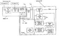
- FIG. 2illustrates a system overview of a supply system according to an embodiment of the invention.
- an A/C source 102may supply A/C power to an adapter 105 .
- a DC source 103may supply DC power to the adapter 105 .
- An example of a power source and an adapter 105is shown in U.S. Pat. No. 6,172,884, the disclosure of which is herein incorporated by reference.
- the adapter 105may include an A/C to DC converter 200 to convert an A/C input into a DC output.
- the adapter 105may also include a selection device 205 .
- the selection device 205may be utilized to select a (a) DC input from a DC source 103 , or (b) a DC output of the A/C to DC converter 200 when the input is A/C power from an A/C source 102 .
- the selection device 205may output the selected DC voltage to a regulation device 210 . Accordingly, the selection device 205 may provide a DC voltage to the regulation device 210 , regardless of whether an A/C source 102 or a DC source 103 is provided to the adapter 105 .
- the regulation device 210may receive the selected DC voltage and provide an output voltage, V out1 . V out1 may be sent via a cable 122 to an active tip 260 .
- the cable 122may include an internal resistance.
- V out1there may be a voltage drop (e.g., V cable ) across the cable 122 .
- V out2when V out1 is output from the adapter 105 to the cable 122 , the cable 122 provides a voltage V out2 to the active tip 260 .
- V out2will not equal V out1 . Instead, V out2 equals V out1 ⁇ V cable .
- the active tip 260may be utilized to control the actual voltage received by the active tip 260 (i.e., V out2 ), and provided to the electronic device 120 without further voltage drops.
- the active tip 260may include active control circuitry to control the V out2 received. Accordingly, the active tip 260 may correct for a voltage drop across the cable 122 so that V out2 can be controlled.
- the adapter 105may provide V out1 and GND to the cable 122 .
- the adapter 105may receive the following outputs from the active tip 260 via the cable 122 : (a) a programming voltage (V prog ) to program V out1 , and (b) a programming current voltage (V Iprog ) to limit the current from the adapter 105 .
- the active tip 260may alter the V prog in order to control V out2 , for example.
- V out2may enter the active tip 260 , and may flow through a switch 240 and out of the active tip 260 to power an external electronic device 120 .
- the switch 240may be utilized to protect the electronic device 120 .
- the active tip 260may detect an error and open the switch 240 so that V out2 does not flow through the switch 240 to the electronic device 120 .
- the switch 240may also be opened when V prog is changed in order to increase V out2 , but V out2 does not correspondingly increase.
- the switch 240may also be opened if the active tip detects excess current. Accordingly, the switch 240 may be utilized to protect the electronic device 120 from becoming oversupplied, for example.
- the active tip 260may include a V prog controller 220 to set V prog .
- the V prog controllermay compare V out2 with a predetermined reference voltage to determine whether V out2 needs to be lowered, raised, or remain constant.
- the V prog controller 220may also divide V out2 by a certain amount before comparing with the reference voltage (e.g., one-half of V out2 may be compared with the reference voltage). If V out2 needs to be lowered, the V prog controller 220 may lower V prog to a level so V out2 is correctly set.
- the V prog output of the V prog controller 220may be output to the regulation device 210 in the adapter 105 .
- the regulation device 210may determine and output V out1 based upon the value of V prog .
- V out1may be equal to the product of V prog multiplied by a factor.
- the regulation device 210may output a V out1 that is 3 times V prog . Therefore, if V prog is 3 volts, V out1 would be 9 volts, and V out2 would be 9 volts minus the V cable .
- the active tip 260may also include circuitry to detect when the adapter 105 is functioning improperly. For example, a voltage error detection device 225 may determine when the relationship between V prog and V out2 is incorrect. If the regulation device 210 is set to output a V out1 that is 3 times V prog , and, for example, if V out2 is detected as being equal to only 1.5 times V prog , then the voltage error detection device 225 may determine that the adapter 105 is functioning improperly. Accordingly, to protect the electronic device 120 , if the voltage error detection device 225 detects an error in the relationship between V prog and V out2 , a signal indicative of the error may be output by the voltage error detection device 225 .
- the active tip 260may also include a current error detection device 242 to detect an error between current output by the regulation device 210 and I prog .
- the active tip 260may include an I prog controller 235 to set V Iprog .
- the I prog controller 235may be a passive device such as a resistor.
- the voltage drop across the I prog controller 235 (i.e., V Iprog ) and V out2may be inputs to the current error detection device 242 .
- the current error detection device 242may determine an error in the functioning of the adapter 105 and may output a signal indicative of the error.
- the outputs of the voltage error detection device 225 and the current error detection device 242may be received by a logical “or” device 230 , which may logically “or” its inputs. If either the voltage error detection device 225 or the current error detection device 242 output a signal indicative of an error, then the logical “or” device 230 may output a signal to open the switch 240 . Accordingly, if the adapter 105 is functioning improperly, the active tip 260 may detect the error and open the switch 240 , preventing the electronic device 120 from being damaged.
- the output of the logical “or” device 230may also be sent to an operation indication device 245 .
- the operation indication device 245may include Light Emitting Diodes (LEDs) to indicate whether the adapter 105 is properly functioning. For example, if a signal indicative of an error is output by the logical “or” device 230 , the operation indication device 245 may include a red LED which is lit up to indicate the error. However, if no such error signal is output by the logical “or” device 230 , a green LED in the operation indication device 245 may be lit, to indicate the correct operation. In other embodiments, devices other than LEDs may be utilized to indicate whether the adapter 105 is functioning properly.
- LEDsLight Emitting Diodes
- FIG. 3illustrates a schematic diagram of an active tip 260 according to an embodiment of the invention.
- a connector 300may be utilized to couple the active tip 260 to the cable 122 .
- V out2may flow into the active tip 260 via pin 2 of the connector 300 , and pin 3 may be coupled to GND.
- Pin 4may be utilized to allow V prog to be sent to the cable 122 , and to the regulation device 210 of the adapter 105 .
- Pin 1may allow V Iprog to be applied to the cable 122 and to the regulation device 210 to limit the current.
- V out2may be utilized to power circuitry in the active tip 260 .
- Resistor RA 305 and a Zener diode VR 1 310lie between V out2 and GND.
- the Zener diode 310may be utilized to set the V cc 315 of the active circuitry in the active tip 260 .
- the active tipmay receive its V cc directly from the adapter 105 .
- Zener diode 310may be utilized to set a maximum voltage of V cc 315 , such as 10 Volts, for example.
- the Zener diode 310may be utilized to protect circuitry in the active tip by limiting the voltage.
- Resistors RB 320 , RC 325 , RD 330are connected between V out2 and GND. Resistors RB 320 , RC 325 , and RD 330 may be utilized to set the inputs to comparator A 340 and comparator B 345 .
- Resistance values of resistors RB 320 , RC 325 , and RD 330 in the active tip 260are selected based on the power requirements of the electronic device 120 being powered. For example, an electronic device requiring 9 volts DC would include different resistance values of resistors RB 320 , RC 325 , and RD 330 than would be used to provide 12 volts DC to a different electronic device. Accordingly, electronic devices 120 having different DC power requirements require active tips 260 having different resistance values.
- Resistors RB 320 , RC 325 , and RD 330form a voltage divider. The voltage divider is utilized to control the voltage received at pin 4 of a voltage regulator 350 .
- the voltage regulator 350is utilized to set V prog , based on a comparison between the voltage received at pin 4 and an internal reference voltage of the voltage regulator 250 (e.g., 2.5 volts). Because RB 320 , RC 325 , and RD 330 form a voltage divider, their resistance values may be utilized to control the percentage of V out2 received at pin 4 of the voltage regulator 350 . Since V prog is set based on a comparison between the voltage regulator's internal voltage and the voltage at pin 4 of the voltage regulator 350 , the resistance values of RB 320 , RC 325 , and RD 330 therefore indirectly control V out2 .
- the voltage regulator 350may, via its pin 4 , receive a voltage equal to V out2 *(RD)/(RB+RC+RD).
- the voltage regulator 350may compare [V out2 *(RD)/(RB+RC+RD)] with an internal reference voltage, such as 2.5 Volts, and output V prog via pin 3 . If [V out2 *(RD)/(RB+RC+RD)] is greater than the internal reference voltage, then V prog may be lowered. Accordingly, in an embodiment where the regulation device 210 outputs V out1 (and the active tip receives V out2 ) that is equal to 3 times V prog , V prog may be increased when V out2 is too low.
- V progmay also be decreased in order to lower V out1 (and correspondingly lower V out2 ) when V out2 is too high. Accordingly, the voltage regulator 350 may serve to control the V out1 produced by the regulation device 210 of the adapter 105 . The voltage regulator 350 therefore sets V prog based on comparison of its internal reference voltage and [V out2 *(RD)/(RB+RC+RD)]. V prog is output back to the regulation device 210 to change V out1 (and correspondingly, V out2 ). Accordingly, the regulation device 210 provides feedback to the adapter 105 so that V out1 (and correspondingly, V out2 ) can be quickly changed as necessary. Due to this feedback, the response time for changing V out1 (and correspondingly, V out2 ) may be decreased over what it would be if there were no feedback from active circuitry.
- the voltage regulator 350not only acts to set the magnitude of V out2 , it also provides additional gain in the feedback loop which compensates for variations in the load of the electronic device 120 .
- the regulation device 210 of the adapter 105has its own response time for changing V out1 (and correspondingly, V out2 ) in response to a load variation. Accordingly, the regulation device 210 of the adapter 105 provides its own gain.
- the regulation device 210 of the adapter 105according to an embodiment of the invention also receives feedback (i.e., V prog ) from the voltage regulator 305 .
- the voltage regulatoris an active device which provides additional gain to the regulation device 210 of the adapter 105 .
- the regulation devicehas greater gain and a quicker response time because the regulation device 210 receives feedback from itself as well as the voltage regulator 305 .
- such combinationalso does not suffer from any voltage drop (i.e., V cable ) due to the resistance of the cable 122 connecting the adapter 105 to the active tip 260 since V out2 is monitored at the point of application to the device, i.e., at the active tip 260 , rather than at the output of the adapter as in prior configurations.
- Comparators A 340 and B 345may be used to control whether transistor Q 1 350 is on (normal operation) or off (failure condition) and whether green LED DS 1 355 (normal operation) or red LED DS 2 360 (failure condition) is illuminated. Comparator A 340 may be utilized as a voltage error detection device 225 .
- comparator A 340When the input to the noninverting input (i.e., V prog ) exceeds the input to the inverting input (i.e., [V out2 *(RC+RD)/(RB+RC+RD)]), as it should during normal operation, comparator A 340 is “off.” If, however, [V out2 *(RC+RD)/(RB+RC+RD)] exceeds V prog , comparator A 340 is said to be “on,” and outputs a low voltage such as GND. The low voltage may indicate that the adapter 105 is operating improperly.
- Resistor RE 335may be utilized as a current programming device (i.e., I prog controller 235 of FIG. 2 ).
- the voltage across resistor RE 335may be input into the noninverting input of comparator B 345 .
- the input to the inverting input of comparator B 345may be [V out2 *(RD)/(RB+RC+RD)].
- Comparator B 345may be utilized as a current error detection device 240 .
- V Iprogwhich is [I prog *RE]
- comparator B 345is off.
- comparator B 345If, however, [V out2 *(RD)/(RB+RC+RD)] exceeds V prog , comparator B 345 is said to be “on,” and outputs a low voltage such as GND. The low voltage may indicate that the adapter 105 is operating improperly.
- LED DS 2 360may be lit. Red LED DS 2 360 may be lit to indicate that an error condition has occurred. If no errors are detected, the green LED DS 1 355 may be lit.
- VCC through RG 385pulls up the base of Q 2 365 , and there is sufficient current to turn on transistor Q 2 365 , thereby pulling low the gate voltage of P-channel FET Q 1 350 to turn it on, and allowing V out2 to be passed through to pin 1 of the connector 370 going to the electronic device 120 being powered.
- comparators A 340 and B 345When one, or both, of comparators A 340 and B 345 detect an improper operation, the low voltage output by them turns off transistor Q 2 360 , thereby turning off FET Q 1 350 to prevent V out2 from being passed to the electronic device 120 .
- comparator A 340 or comparator B 345If either comparator A 340 or comparator B 345 is on (e.g., either one outputs GND), then current may flow from Vcc through red LED DS 2 360 , and then to GND. Accordingly, if either comparator A 340 or comparator B 345 is on, the current will cause red LED DS 2 360 to become lit, but not green LED DS 1 355 .
- Resistors RB 320 , RC 325 , and RD 330may be different values, depending upon the type of electronic device 120 being powered by the active tip 260 .
- Resistors RB 320 , RC 325 , and RD 330are utilized for voltage division. Accordingly, resistors RB 320 , RC 325 , and RD 330 vary from active tip 260 to active tip 260 , depending upon the amount of V out2 to be supplied to the electronic device 120 .
- a specific active tip 260may be utilized to supply power to an electronic device 120 having specified power requirements. Accordingly, when a device having different power requirements is to be utilized, the active tip 260 may be replaced with a different active tip 260 having different resistor values RB 320 , RC 325 , RD 330 , and RJ 390 .
- the voltage regulator 350may be a TL431 or TLV431 shunt regulator produced by Texas Instruments, for example.
- Comparators A 340 and B 345may be dual differential comparators such as the following models produced by Texas Instruments: LM193, LM293, LM293A, LM393, LM393A, LM2903, or LM2903Q, for example.
- FIG. 4Aillustrates a response time (not drawn to scale) of an adapter 105 after a fluctuation in voltage according to the prior art.
- the vertical axisrepresents voltage
- the horizontal axisrepresents time.
- the adapter 105may output X volts.
- the cable 122may have an internal resistance, resulting in a voltage drop (e.g., Y volts) when current is being drawn by the device. Accordingly, voltage reaching the electronic device 120 may equal X-Y volts. If no current is being drawn by the device, the voltage supplied to the device (i.e., the open circuit voltage) is X volts, which case is shown in FIG. 4A .
- the voltagemay suddenly drop, eventually down to a low of M 1 volts, until the adapter 105 responds by increasing the voltage back up, so that the output of the cable 122 is X-Y volts. As shown, the voltage does not recover until time T 2 .
- FIG. 4Billustrates the magnitude of current flowing out of the adapter to the electronic device according to an embodiment of the invention.
- no currentflows from the adapter 105 through the cable 122 and on into the electronic device 120 .
- the currentincreases to Y amps.
- the increase in the currentresults in a voltage drop across the cable 122 , as shown in FIG. 4A .
- the currentincreases, and a voltage drop across the cable 122 is realized before the power source 100 has a chance to compensate (due its delayed response time).
- the voltage supplied to the electronic device 120increases to X-Y volts, where Y is the voltage drop across the cable 122 .
- FIG. 4Cillustrates a response time (not drawn to scale) of the system having the adapter 105 coupled to the active tip 260 according to an embodiment of the invention.
- the output of the cable 122is X volts.
- the output of the cable 122may be precisely set due to the active circuitry in the active tip 260 .
- the loadmay increase (as shown in FIG. 4B ), pulling down the voltage.
- the active tip 260may sense the decrease in the voltage, and may increase V prog accordingly, raising the output voltage back up to X volts.
- the trough of the voltageis M 2 volts.
- the trough M 2is higher than the trough M 1 of the prior art.
- the time period during which the voltage dips below the correct amountis shorter than that of the prior art.
- the prior arthas a response time equal to (T 2 ⁇ T 1 ), but the response time of the system having the active tip 260 is shorter, (T 3 ⁇ T 1 ).
- the active tip systemhas a lower response time due to greater loop gain than adapters 105 of the prior art. Because of the gain in the tip (due to the voltage regulator 350 ), the regulation device 210 of the adapter 105 has a faster response time and, after compensation, raises the voltage at the tip back up to X volts.
- FIG. 5Aillustrates a first portion of a method of supplying power to an electronic device 120 via an adapter 105 and active tip 260 according to an embodiment of the invention.
- the adaptermay receive 500 power from a power source 100 .
- the adapter 105may receive 505 V prog .
- the adapter 105may then create V out by multiplying 510 V prog times a multiplication factor.
- V outmay be outputted 515 to the active tip 260 .
- the active tip 260may create 520 V prog .
- the active tip 260may then create 525 I prog .
- V progis compared with V out , or a factor of V out , to determine 530 whether there is an error.
- processingproceeds to operation 550 . If “no,” the voltage drop across the I prog controller 235 (i.e., V Iprog ) is compared with V out , or a factor of V out , to determine 535 whether there is an error. If “yes,” processing proceeds to operation 550 . If “no,” processing proceeds to operation 540 .
- FIG. 5Billustrates a second portion of the method of supplying power to an electronic device 120 via an adapter 105 and active tip 260 according to an embodiment of the invention.
- LED DS 1 355is lit 540 to indicate proper operation.
- transistor Q 1 350i.e., switch 240
- LED DS 2 360is lit to indicate improper operation.
- transistor Q 1 350i.e., switch 240
- processingreverts to operation 500 .
Landscapes
- Engineering & Computer Science (AREA)
- Power Engineering (AREA)
- Physics & Mathematics (AREA)
- Electromagnetism (AREA)
- General Physics & Mathematics (AREA)
- Radar, Positioning & Navigation (AREA)
- Automation & Control Theory (AREA)
- Dc-Dc Converters (AREA)
- Electrophonic Musical Instruments (AREA)
- Channel Selection Circuits, Automatic Tuning Circuits (AREA)
- Control Of Combustion (AREA)
- Logic Circuits (AREA)
- Amplifiers (AREA)
Abstract
Description
Claims (20)
Priority Applications (2)
| Application Number | Priority Date | Filing Date | Title |
|---|---|---|---|
| US10/927,619US7193398B2 (en) | 2002-12-05 | 2004-08-26 | Tip having active circuitry |
| US11/725,612US7365524B2 (en) | 2002-12-05 | 2007-03-20 | Tip having active circuitry |
Applications Claiming Priority (2)
| Application Number | Priority Date | Filing Date | Title |
|---|---|---|---|
| US10/313,662US6836101B2 (en) | 2002-12-05 | 2002-12-05 | Tip having active circuitry |
| US10/927,619US7193398B2 (en) | 2002-12-05 | 2004-08-26 | Tip having active circuitry |
Related Parent Applications (1)
| Application Number | Title | Priority Date | Filing Date |
|---|---|---|---|
| US10/313,662ContinuationUS6836101B2 (en) | 2002-12-05 | 2002-12-05 | Tip having active circuitry |
Related Child Applications (1)
| Application Number | Title | Priority Date | Filing Date |
|---|---|---|---|
| US11/725,612ContinuationUS7365524B2 (en) | 2002-12-05 | 2007-03-20 | Tip having active circuitry |
Publications (2)
| Publication Number | Publication Date |
|---|---|
| US20050024030A1 US20050024030A1 (en) | 2005-02-03 |
| US7193398B2true US7193398B2 (en) | 2007-03-20 |
Family
ID=32468312
Family Applications (3)
| Application Number | Title | Priority Date | Filing Date |
|---|---|---|---|
| US10/313,662Expired - LifetimeUS6836101B2 (en) | 2002-12-05 | 2002-12-05 | Tip having active circuitry |
| US10/927,619Expired - Fee RelatedUS7193398B2 (en) | 2002-12-05 | 2004-08-26 | Tip having active circuitry |
| US11/725,612Expired - Fee RelatedUS7365524B2 (en) | 2002-12-05 | 2007-03-20 | Tip having active circuitry |
Family Applications Before (1)
| Application Number | Title | Priority Date | Filing Date |
|---|---|---|---|
| US10/313,662Expired - LifetimeUS6836101B2 (en) | 2002-12-05 | 2002-12-05 | Tip having active circuitry |
Family Applications After (1)
| Application Number | Title | Priority Date | Filing Date |
|---|---|---|---|
| US11/725,612Expired - Fee RelatedUS7365524B2 (en) | 2002-12-05 | 2007-03-20 | Tip having active circuitry |
Country Status (4)
| Country | Link |
|---|---|
| US (3) | US6836101B2 (en) |
| EP (1) | EP1462904B1 (en) |
| AT (1) | ATE475220T1 (en) |
| DE (1) | DE60333436D1 (en) |
Cited By (9)
| Publication number | Priority date | Publication date | Assignee | Title |
|---|---|---|---|---|
| US20090051325A1 (en)* | 2007-08-21 | 2009-02-26 | Ford Global Technologies, Llc | Automotive power system and method of controlling same |
| US20090134852A1 (en)* | 2007-11-26 | 2009-05-28 | Liming Sun | System and method using a current mirror to program an output voltage and current |
| US7646107B2 (en) | 2004-09-30 | 2010-01-12 | Targus Group Internatnional, Inc. | Programmable power adaptor |
| US20100254162A1 (en)* | 2009-04-01 | 2010-10-07 | Comarco Wireless Technologies, Inc. | Modular power adapter |
| US20110095605A1 (en)* | 2009-10-28 | 2011-04-28 | Comarco Wireless Technologies, Inc. | Power supply equipment to simultaneously power multiple electronic device |
| US8550827B1 (en) | 2012-07-25 | 2013-10-08 | Targus Group International, Inc. | Multi-sleeve power tips |
| US8821199B2 (en) | 2012-07-25 | 2014-09-02 | Targus Group International, Inc. | Multi-prong power tip adaptor |
| US9153960B2 (en) | 2004-01-15 | 2015-10-06 | Comarco Wireless Technologies, Inc. | Power supply equipment utilizing interchangeable tips to provide power and a data signal to electronic devices |
| US9413187B2 (en) | 2004-01-15 | 2016-08-09 | Comarco Wireless Technologies, Inc. | Power supply system providing power and analog data signal for use by portable electronic device to control battery charging |
Families Citing this family (31)
| Publication number | Priority date | Publication date | Assignee | Title |
|---|---|---|---|---|
| US6836101B2 (en) | 2002-12-05 | 2004-12-28 | Comarco Wireless Technologies, Inc. | Tip having active circuitry |
| US7145312B2 (en)* | 2002-12-06 | 2006-12-05 | Comarco Wireless Technologies, Inc. | Battery coupled to adapter and tip |
| US7148659B2 (en)* | 2003-06-20 | 2006-12-12 | Comarco Wireless Technologies, Inc. | Programmable AC/DC power supply |
| US7526659B2 (en)* | 2005-02-01 | 2009-04-28 | Hewlett-Packard Development Company, L.P. | Systems and methods for controlling use of power in a computer system |
| US7853818B2 (en)* | 2005-02-25 | 2010-12-14 | Intel Corporation | Modifying power adapter output |
| FR2892209A1 (en)* | 2005-10-18 | 2007-04-20 | Jean Louis Lombard | Regulated power supply device for e.g. telephony device, has feedback loop that stabilizes input voltage of offset regulator and controls output voltage of primary supply regulator to correct any voltage drop induced in cables |
| US8266348B2 (en)* | 2005-11-08 | 2012-09-11 | American Power Conversion Corporation | System and method of communicating with portable devices |
| US20070229024A1 (en)* | 2006-03-30 | 2007-10-04 | Li Peter T | Balancing power supply and demand |
| US7642671B2 (en) | 2006-04-28 | 2010-01-05 | Acco Brands Usa Llc | Power supply system providing two output voltages |
| US20090108677A1 (en)* | 2007-10-29 | 2009-04-30 | Linear Technology Corporation | Bidirectional power converters |
| US8093875B2 (en)* | 2007-11-26 | 2012-01-10 | Igo, Inc. | System and method for cable resistance cancellation |
| JPWO2009075313A1 (en)* | 2007-12-13 | 2011-04-28 | トヨタ自動車株式会社 | Electricity amount calculation device, fee calculation device and fee calculation method for calculating fee for power consumption, vehicle information output device and information output method |
| TW201005460A (en)* | 2008-07-23 | 2010-02-01 | Kerio Technologies Inc | Safety output device for power converter and power converter having the same |
| TW201014100A (en)* | 2008-09-24 | 2010-04-01 | Kerio Technologies Inc | Output voltage feedback device for a power supply and the power supply thereof |
| TW201025783A (en)* | 2008-12-31 | 2010-07-01 | Kerio Technologies Inc | Output voltage feedback device with feedback line for power supply and the power supply |
| US8536840B2 (en)* | 2009-03-17 | 2013-09-17 | Linear Technology Corporation | Bidirectional power converters |
| US20110015795A1 (en)* | 2009-07-16 | 2011-01-20 | International Business Machines Corporation | Smart Outlet with Valid Plug Management and Activation |
| US9118240B2 (en)* | 2011-08-31 | 2015-08-25 | Comarco Wireless Technologies, Inc. | Power supply equipment providing multiple identification signals |
| JP2013223389A (en)* | 2012-04-19 | 2013-10-28 | Smk Corp | Power supply system |
| US9271063B2 (en) | 2013-02-06 | 2016-02-23 | Zeikos Inc. | Power transferring headphones |
| US9276539B2 (en) | 2013-02-06 | 2016-03-01 | Zeikos Inc. | Power transferring headphones |
| US20140219465A1 (en) | 2013-02-06 | 2014-08-07 | Zeikos Inc. | Power transferring headphones |
| SG11201606219XA (en)* | 2014-01-28 | 2016-09-29 | Guang Dong Oppo Mobile Telecomm Corp Ltd | Terminal, power adapter and method for handling charging anomaly |
| DK3101770T3 (en)* | 2014-01-28 | 2019-07-22 | Guangdong Oppo Mobile Telecommunications Corp Ltd | POWER ADAPTERS AND TERMINAL |
| SG11201606222UA (en) | 2014-01-28 | 2016-08-30 | Guang Dong Oppo Mobile Telecomm Corp Ltd | Power adapter, terminal, and method for processing impedance exception of charging loop |
| US9715244B2 (en)* | 2015-02-24 | 2017-07-25 | Intersil Americas LLC | System and method for determining adapter current limit |
| EP3206279B1 (en)* | 2015-12-16 | 2020-11-11 | Guangdong Oppo Mobile Telecommunications Corp., Ltd. | Charging control method and device, power adapter, and mobile terminal |
| JP6711730B2 (en)* | 2016-09-27 | 2020-06-17 | ホシデン株式会社 | Power supply |
| US11271384B2 (en)* | 2017-07-27 | 2022-03-08 | Western Technology, Inc. | Power supply interlock |
| KR102557297B1 (en)* | 2018-09-30 | 2023-07-20 | 광동 오포 모바일 텔레커뮤니케이션즈 코포레이션 리미티드 | Adapter functional test method and device, equipment, storage medium |
| CN111077930A (en)* | 2019-12-17 | 2020-04-28 | 太原航空仪表有限公司 | Energy storage circuit power failure monitoring trigger circuit |
Citations (52)
| Publication number | Priority date | Publication date | Assignee | Title |
|---|---|---|---|---|
| US2914704A (en) | 1955-10-31 | 1959-11-24 | Gilfillan Bros Inc | Abnormal voltage protection circuit |
| US3048805A (en) | 1960-10-04 | 1962-08-07 | Ace Electronics Associates Inc | Plug-in potentiometers |
| US3049687A (en) | 1959-08-26 | 1962-08-14 | Ace Electronics Associates Inc | Plug-in variable resistor |
| US3111641A (en) | 1961-02-03 | 1963-11-19 | Jerzy J Wilentchik | Plug and jack resistor |
| US3978465A (en) | 1974-10-25 | 1976-08-31 | Esb Incorporated | Line isolation monitor |
| US4257089A (en) | 1979-09-13 | 1981-03-17 | The United States Of America As Represented By The Secretary Of The Army | Regulated variable frequency DC/DC converter |
| US4307441A (en) | 1980-07-28 | 1981-12-22 | United Technologies Corporation | Current balanced DC-to-DC converter |
| US4442382A (en) | 1982-07-06 | 1984-04-10 | Chiu Technical Corporation | Constant power switching power supply |
| US4622627A (en) | 1984-02-16 | 1986-11-11 | Theta-J Corporation | Switching electrical power supply utilizing miniature inductors integrally in a PCB |
| US4734839A (en) | 1987-03-23 | 1988-03-29 | Barthold Fred O | Source volt-ampere/load volt-ampere differential converter |
| US4747034A (en) | 1987-03-05 | 1988-05-24 | David V. Dickey | High efficiency battery adapter |
| US4885674A (en) | 1988-03-28 | 1989-12-05 | Varga Ljubomir D | Synthesis of load-independent switch-mode power converters |
| US4890214A (en) | 1985-11-15 | 1989-12-26 | Nec Corporation | Start circuit for adapting a constant current generator to a wide variety of loads |
| US4912392A (en) | 1986-10-18 | 1990-03-27 | Husky Computer Limited | Battery charge state monitor |
| US5019954A (en) | 1989-06-23 | 1991-05-28 | Allied-Signal Inc. | AC/DC conversion with reduced supply waveform distortion |
| US5146394A (en) | 1989-06-23 | 1992-09-08 | Matsushita Electric Industrial Co., Ltd. | Fly back converter switching power supply device |
| US5177431A (en)* | 1991-09-25 | 1993-01-05 | Astec International Ltd. | Linear programming circuit for adjustable output voltage power converters |
| US5177675A (en) | 1991-10-16 | 1993-01-05 | Shindengen Archer Corp. | Zero voltage, zero current, resonant converter |
| US5184291A (en) | 1991-06-13 | 1993-02-02 | Crowe Lawrence E | Converter and inverter support module |
| USD339103S (en) | 1992-07-02 | 1993-09-07 | Empire Engineering | Housing for an AC power adapter |
| US5295058A (en) | 1992-10-13 | 1994-03-15 | Recoton Corporation | Universal DC to DC power converter |
| US5309348A (en) | 1992-08-13 | 1994-05-03 | Acer Peripherals, Inc. | Method and apparatus for preventing improper switching of a dual power supply |
| US5345592A (en) | 1992-04-08 | 1994-09-06 | Concept W Systems, Inc. | Signal transfer and power delivery system for a television camera station |
| US5347211A (en) | 1993-03-11 | 1994-09-13 | Innova Electronics Corporation | Selectable output power converter |
| USD359474S (en) | 1994-04-13 | 1995-06-20 | Xtend Micro Products, Inc. | Modular drop charger for portable electronic equipment |
| US5479331A (en) | 1994-04-26 | 1995-12-26 | Comarco Wireless Technologies, Inc. | Small form factor power supply |
| US5510691A (en) | 1994-04-13 | 1996-04-23 | Xtend Micro Products, Inc | Modular power supply and modular interconnect system for portable electronic equipment |
| US5559422A (en) | 1994-07-01 | 1996-09-24 | Welch Allyn, Inc. | Wall transformer |
| USD375936S (en) | 1995-08-25 | 1996-11-26 | Xtend Micro Products, Inc. | Modular drop charger and DC-DC converter for portable electronic equipment |
| US5589762A (en)* | 1991-02-22 | 1996-12-31 | Sgs-Thomson Microelectronics, Inc. | Adaptive voltage regulator |
| US5636110A (en) | 1994-04-26 | 1997-06-03 | Comarco Wireless Technologies, Inc. | Small form factor power supply |
| US5672951A (en) | 1994-11-04 | 1997-09-30 | Mitsubishi Denki Kabushiki Kaisha | Determination and control of battery state |
| US5717318A (en)* | 1996-07-08 | 1998-02-10 | Fujitsu Limited | Step-down type DC-DC regulator |
| USD391227S (en) | 1996-01-29 | 1998-02-24 | Empire Engineering | Smart adapter |
| US5739672A (en) | 1996-05-08 | 1998-04-14 | United Continental | Method and apparatus for charging batteries |
| US5739673A (en) | 1996-02-27 | 1998-04-14 | Sgs-Thomson Microelectronics S.A. | Control device for the charging of at least one battery |
| US5770895A (en) | 1995-06-08 | 1998-06-23 | Tokyo Electron Limited | Operation control device and method for a plurality of electric power consuming systems |
| US5773961A (en) | 1996-06-06 | 1998-06-30 | Heartstream, Inc. | Dynamic load controller for a battery |
| US5838554A (en) | 1994-04-26 | 1998-11-17 | Comarco Wireless Technologies, Inc. | Small form factor power supply |
| US5861732A (en) | 1989-12-11 | 1999-01-19 | Canon Kabushiki Kaisha | Battery charging apparatus |
| US5886422A (en) | 1997-07-30 | 1999-03-23 | Spartec International Corporation | Universal electric power controller |
| US5949213A (en) | 1994-04-26 | 1999-09-07 | Comarco Wireless Technologies, Inc. | Method and system for charging rechargeable batteries |
| US6064177A (en) | 1999-01-05 | 2000-05-16 | Dixon; Steven C. | Two-part battery charger/power cable article with multiple device capability |
| US6091611A (en) | 1994-04-26 | 2000-07-18 | Comarco Wireless Technologies, Inc. | Connectors adapted for controlling a small form factor power supply |
| US6172884B1 (en) | 1994-04-26 | 2001-01-09 | Comarco Wireless Technologies, Inc. | Small form factor power supply for powering electronics appliances |
| US6194875B1 (en) | 1998-10-08 | 2001-02-27 | Fujitsu Limited | Controller for DC-DC converter |
| US6201376B1 (en)* | 2000-01-28 | 2001-03-13 | Lucent Technologies Inc. | Apparatus and method for establishing an operating parameter for a power supply device |
| DE20113817U1 (en) | 2001-08-21 | 2001-11-08 | Lumberg Karl Gmbh & Co | Electrical connector |
| US6670797B2 (en) | 2000-03-17 | 2003-12-30 | Siemens Aktiengesellschaft | Method and device for controlling a dc-dc converter |
| US6678178B2 (en) | 2000-10-26 | 2004-01-13 | Micro International Limited | DC-to-DC converter with improved transient response |
| US6703815B2 (en)* | 2002-05-20 | 2004-03-09 | Texas Instruments Incorporated | Low drop-out regulator having current feedback amplifier and composite feedback loop |
| US6836101B2 (en)* | 2002-12-05 | 2004-12-28 | Comarco Wireless Technologies, Inc. | Tip having active circuitry |
Family Cites Families (4)
| Publication number | Priority date | Publication date | Assignee | Title |
|---|---|---|---|---|
| US391227A (en) | 1888-10-16 | Tool for crimping metal | ||
| US339103A (en) | 1886-03-30 | Silvanus hussey | ||
| US359474A (en) | 1887-03-15 | Levi smith | ||
| US375936A (en) | 1888-01-03 | Projectile for fire-arms |
- 2002
- 2002-12-05USUS10/313,662patent/US6836101B2/ennot_activeExpired - Lifetime
- 2003
- 2003-12-05EPEP03257679Apatent/EP1462904B1/ennot_activeExpired - Lifetime
- 2003-12-05DEDE60333436Tpatent/DE60333436D1/ennot_activeExpired - Lifetime
- 2003-12-05ATAT03257679Tpatent/ATE475220T1/ennot_activeIP Right Cessation
- 2004
- 2004-08-26USUS10/927,619patent/US7193398B2/ennot_activeExpired - Fee Related
- 2007
- 2007-03-20USUS11/725,612patent/US7365524B2/ennot_activeExpired - Fee Related
Patent Citations (52)
| Publication number | Priority date | Publication date | Assignee | Title |
|---|---|---|---|---|
| US2914704A (en) | 1955-10-31 | 1959-11-24 | Gilfillan Bros Inc | Abnormal voltage protection circuit |
| US3049687A (en) | 1959-08-26 | 1962-08-14 | Ace Electronics Associates Inc | Plug-in variable resistor |
| US3048805A (en) | 1960-10-04 | 1962-08-07 | Ace Electronics Associates Inc | Plug-in potentiometers |
| US3111641A (en) | 1961-02-03 | 1963-11-19 | Jerzy J Wilentchik | Plug and jack resistor |
| US3978465A (en) | 1974-10-25 | 1976-08-31 | Esb Incorporated | Line isolation monitor |
| US4257089A (en) | 1979-09-13 | 1981-03-17 | The United States Of America As Represented By The Secretary Of The Army | Regulated variable frequency DC/DC converter |
| US4307441A (en) | 1980-07-28 | 1981-12-22 | United Technologies Corporation | Current balanced DC-to-DC converter |
| US4442382A (en) | 1982-07-06 | 1984-04-10 | Chiu Technical Corporation | Constant power switching power supply |
| US4622627A (en) | 1984-02-16 | 1986-11-11 | Theta-J Corporation | Switching electrical power supply utilizing miniature inductors integrally in a PCB |
| US4890214A (en) | 1985-11-15 | 1989-12-26 | Nec Corporation | Start circuit for adapting a constant current generator to a wide variety of loads |
| US4912392A (en) | 1986-10-18 | 1990-03-27 | Husky Computer Limited | Battery charge state monitor |
| US4747034A (en) | 1987-03-05 | 1988-05-24 | David V. Dickey | High efficiency battery adapter |
| US4734839A (en) | 1987-03-23 | 1988-03-29 | Barthold Fred O | Source volt-ampere/load volt-ampere differential converter |
| US4885674A (en) | 1988-03-28 | 1989-12-05 | Varga Ljubomir D | Synthesis of load-independent switch-mode power converters |
| US5019954A (en) | 1989-06-23 | 1991-05-28 | Allied-Signal Inc. | AC/DC conversion with reduced supply waveform distortion |
| US5146394A (en) | 1989-06-23 | 1992-09-08 | Matsushita Electric Industrial Co., Ltd. | Fly back converter switching power supply device |
| US5861732A (en) | 1989-12-11 | 1999-01-19 | Canon Kabushiki Kaisha | Battery charging apparatus |
| US5589762A (en)* | 1991-02-22 | 1996-12-31 | Sgs-Thomson Microelectronics, Inc. | Adaptive voltage regulator |
| US5184291A (en) | 1991-06-13 | 1993-02-02 | Crowe Lawrence E | Converter and inverter support module |
| US5177431A (en)* | 1991-09-25 | 1993-01-05 | Astec International Ltd. | Linear programming circuit for adjustable output voltage power converters |
| US5177675A (en) | 1991-10-16 | 1993-01-05 | Shindengen Archer Corp. | Zero voltage, zero current, resonant converter |
| US5345592A (en) | 1992-04-08 | 1994-09-06 | Concept W Systems, Inc. | Signal transfer and power delivery system for a television camera station |
| USD339103S (en) | 1992-07-02 | 1993-09-07 | Empire Engineering | Housing for an AC power adapter |
| US5309348A (en) | 1992-08-13 | 1994-05-03 | Acer Peripherals, Inc. | Method and apparatus for preventing improper switching of a dual power supply |
| US5295058A (en) | 1992-10-13 | 1994-03-15 | Recoton Corporation | Universal DC to DC power converter |
| US5347211A (en) | 1993-03-11 | 1994-09-13 | Innova Electronics Corporation | Selectable output power converter |
| USD359474S (en) | 1994-04-13 | 1995-06-20 | Xtend Micro Products, Inc. | Modular drop charger for portable electronic equipment |
| US5510691A (en) | 1994-04-13 | 1996-04-23 | Xtend Micro Products, Inc | Modular power supply and modular interconnect system for portable electronic equipment |
| US5479331A (en) | 1994-04-26 | 1995-12-26 | Comarco Wireless Technologies, Inc. | Small form factor power supply |
| US5838554A (en) | 1994-04-26 | 1998-11-17 | Comarco Wireless Technologies, Inc. | Small form factor power supply |
| US5636110A (en) | 1994-04-26 | 1997-06-03 | Comarco Wireless Technologies, Inc. | Small form factor power supply |
| US6172884B1 (en) | 1994-04-26 | 2001-01-09 | Comarco Wireless Technologies, Inc. | Small form factor power supply for powering electronics appliances |
| US6091611A (en) | 1994-04-26 | 2000-07-18 | Comarco Wireless Technologies, Inc. | Connectors adapted for controlling a small form factor power supply |
| US5949213A (en) | 1994-04-26 | 1999-09-07 | Comarco Wireless Technologies, Inc. | Method and system for charging rechargeable batteries |
| US5559422A (en) | 1994-07-01 | 1996-09-24 | Welch Allyn, Inc. | Wall transformer |
| US5672951A (en) | 1994-11-04 | 1997-09-30 | Mitsubishi Denki Kabushiki Kaisha | Determination and control of battery state |
| US5770895A (en) | 1995-06-08 | 1998-06-23 | Tokyo Electron Limited | Operation control device and method for a plurality of electric power consuming systems |
| USD375936S (en) | 1995-08-25 | 1996-11-26 | Xtend Micro Products, Inc. | Modular drop charger and DC-DC converter for portable electronic equipment |
| USD391227S (en) | 1996-01-29 | 1998-02-24 | Empire Engineering | Smart adapter |
| US5739673A (en) | 1996-02-27 | 1998-04-14 | Sgs-Thomson Microelectronics S.A. | Control device for the charging of at least one battery |
| US5739672A (en) | 1996-05-08 | 1998-04-14 | United Continental | Method and apparatus for charging batteries |
| US5773961A (en) | 1996-06-06 | 1998-06-30 | Heartstream, Inc. | Dynamic load controller for a battery |
| US5717318A (en)* | 1996-07-08 | 1998-02-10 | Fujitsu Limited | Step-down type DC-DC regulator |
| US5886422A (en) | 1997-07-30 | 1999-03-23 | Spartec International Corporation | Universal electric power controller |
| US6194875B1 (en) | 1998-10-08 | 2001-02-27 | Fujitsu Limited | Controller for DC-DC converter |
| US6064177A (en) | 1999-01-05 | 2000-05-16 | Dixon; Steven C. | Two-part battery charger/power cable article with multiple device capability |
| US6201376B1 (en)* | 2000-01-28 | 2001-03-13 | Lucent Technologies Inc. | Apparatus and method for establishing an operating parameter for a power supply device |
| US6670797B2 (en) | 2000-03-17 | 2003-12-30 | Siemens Aktiengesellschaft | Method and device for controlling a dc-dc converter |
| US6678178B2 (en) | 2000-10-26 | 2004-01-13 | Micro International Limited | DC-to-DC converter with improved transient response |
| DE20113817U1 (en) | 2001-08-21 | 2001-11-08 | Lumberg Karl Gmbh & Co | Electrical connector |
| US6703815B2 (en)* | 2002-05-20 | 2004-03-09 | Texas Instruments Incorporated | Low drop-out regulator having current feedback amplifier and composite feedback loop |
| US6836101B2 (en)* | 2002-12-05 | 2004-12-28 | Comarco Wireless Technologies, Inc. | Tip having active circuitry |
Non-Patent Citations (13)
| Title |
|---|
| "NEW PowerXtenders Adapter Lets Portable Comuter Users Plug Into Computer Power On Airplanes And Cars," [on-line], Apr. 30, 1997, [retrieved Feb. 13, 2001], pp. 1-3, retrieved from Internet: http://www.roadwarrior.com/xtend/news/pressreleases/pr-970420.html. |
| "Portable Computers Fly High in the Sky with Airline Seat Power," [on-line], Nov. 18, 1996 [retrieved Feb. 13, 2001], pp. 1-2, retrieved from Internet: http://www.roadwarrior.com/xtend/news/pressreleases/pr-961118.html. |
| Data Sheet for Benchmarq Model BQ2002C, Fast-Charge IC, Sep. 1997, 8 pages. |
| Data Sheet for Benchmarq Model BQ2954, Lithium Ion Fast-Charge IC, Nov. 1997, 14 pages. |
| Declaration of David Dickey in Opposition to Comarco's Motion for Summary Judgment, dated Jun. 2, 2003, 8-pgs w/Exhibits 1-13 attached. |
| Declaration of David Dickey in Support of Mobility Electronics, Inc.'s Motion for Summary Judgment, dated Jun. 2, 2003, 8-pgs w/Exhibits 1-13 attached. |
| Declaration of Ejaz Afzal in Opposition to Comarco's Motion for Preliminary Injunction, dated Apr. 30, 2003, 9-pgs w/Exhibits 1-2 attached. |
| Declaration of Ejaz Afzal in Support of Mobility Electronics, Inc.'s Motion for Summary Judgment, dated May 6, 2003, 10-pgs w/Exhibits 1-2 attached. |
| Description of the "Smart Adapter System", Nesco Battery Systems, pp. 1-2. |
| European Search Report from European Patent Office, Jun. 21, 2005, EP Application No. EP 03 25 7679. |
| MacWorld "On the Road", vol. 12, No. 7, Jul. 1995, pp. 141-142, 5/9/1 (Item 1 from file: 15) DIALOG(r) File 15:ABI/INFORM(r). |
| Motorola: Analog IC Device Data, DC-to-DC Converter Circuits-vol. 1, DL 128/D-Revision 6, 1996, XP002330527. |
| Press Release of Empire Engineering, Electronic Design and Management, Jul. 5, 1995-San Luis Obispo, CA USA, pp. 1-2. |
Cited By (20)
| Publication number | Priority date | Publication date | Assignee | Title |
|---|---|---|---|---|
| US9153960B2 (en) | 2004-01-15 | 2015-10-06 | Comarco Wireless Technologies, Inc. | Power supply equipment utilizing interchangeable tips to provide power and a data signal to electronic devices |
| US11586233B2 (en) | 2004-01-15 | 2023-02-21 | Comarco Wireless Systems Llc | Power supply systems |
| US10951042B2 (en) | 2004-01-15 | 2021-03-16 | Comarco Wireless Systems Llc | Power supply systems |
| US10855087B1 (en) | 2004-01-15 | 2020-12-01 | Comarco Wireless Systems Llc | Power supply systems |
| US10855086B2 (en) | 2004-01-15 | 2020-12-01 | Comarco Wireless Systems Llc | Power supply equipment utilizing interchangeable tips to provide power and a data signal to electronic devices |
| US9806548B2 (en) | 2004-01-15 | 2017-10-31 | Comarco Wireless Technologies, Inc. | Power supply system providing power and analog data signal for use by portable electronic device to control battery charging |
| US9647477B2 (en) | 2004-01-15 | 2017-05-09 | Comarco Wireless Technologies, Inc. | Power supply equipment utilizing interchangeable tips to provide power and a data signal to electronic devices |
| US9601922B2 (en) | 2004-01-15 | 2017-03-21 | Comarco Wireless Technologies, Inc. | Power supply equipment utilizing interchangeable tips to provide power and a data signal to electronic devices |
| US9413187B2 (en) | 2004-01-15 | 2016-08-09 | Comarco Wireless Technologies, Inc. | Power supply system providing power and analog data signal for use by portable electronic device to control battery charging |
| US7646107B2 (en) | 2004-09-30 | 2010-01-12 | Targus Group Internatnional, Inc. | Programmable power adaptor |
| US9007031B2 (en) | 2007-08-21 | 2015-04-14 | Ford Global Technologies, Llc | Automotive voltage compensation system and method |
| US20090051325A1 (en)* | 2007-08-21 | 2009-02-26 | Ford Global Technologies, Llc | Automotive power system and method of controlling same |
| US8232785B2 (en)* | 2007-11-26 | 2012-07-31 | Igo, Inc. | System and method using a current mirror to program an output voltage and current |
| US20090134852A1 (en)* | 2007-11-26 | 2009-05-28 | Liming Sun | System and method using a current mirror to program an output voltage and current |
| US8213204B2 (en) | 2009-04-01 | 2012-07-03 | Comarco Wireless Technologies, Inc. | Modular power adapter |
| US20100254162A1 (en)* | 2009-04-01 | 2010-10-07 | Comarco Wireless Technologies, Inc. | Modular power adapter |
| US8354760B2 (en) | 2009-10-28 | 2013-01-15 | Comarco Wireless Technologies, Inc. | Power supply equipment to simultaneously power multiple electronic device |
| US20110095605A1 (en)* | 2009-10-28 | 2011-04-28 | Comarco Wireless Technologies, Inc. | Power supply equipment to simultaneously power multiple electronic device |
| US8821199B2 (en) | 2012-07-25 | 2014-09-02 | Targus Group International, Inc. | Multi-prong power tip adaptor |
| US8550827B1 (en) | 2012-07-25 | 2013-10-08 | Targus Group International, Inc. | Multi-sleeve power tips |
Also Published As
| Publication number | Publication date |
|---|---|
| US7365524B2 (en) | 2008-04-29 |
| US20050024030A1 (en) | 2005-02-03 |
| EP1462904B1 (en) | 2010-07-21 |
| ATE475220T1 (en) | 2010-08-15 |
| US20070182388A1 (en) | 2007-08-09 |
| US6836101B2 (en) | 2004-12-28 |
| US20040108843A1 (en) | 2004-06-10 |
| EP1462904A2 (en) | 2004-09-29 |
| DE60333436D1 (en) | 2010-09-02 |
| EP1462904A3 (en) | 2005-08-03 |
| HK1068171A1 (en) | 2005-04-22 |
Similar Documents
| Publication | Publication Date | Title |
|---|---|---|
| US7193398B2 (en) | Tip having active circuitry | |
| US4779037A (en) | Dual input low dropout voltage regulator | |
| US6465909B1 (en) | Circuits and methods for controlling load sharing by multiple power supplies | |
| US5629609A (en) | Method and apparatus for improving the drop-out voltage in a low drop out voltage regulator | |
| CN110058631B (en) | Voltage regulator with feed forward circuit | |
| US20070229149A1 (en) | Voltage regulator having high voltage protection | |
| US7911191B2 (en) | Drop-out voltage monitoring method and apparatus | |
| US7248026B2 (en) | Single-pin tracking/soft-start function with timer control | |
| CN100538868C (en) | Be used to reduce the internal power voltage generator of current drain | |
| US10770894B1 (en) | Fast settlement of supplement converter for power loss protection system | |
| CN100583637C (en) | pull-up circuit | |
| US5845141A (en) | Method and apparatus for the remote programming of a power supply | |
| US6876180B2 (en) | Power supply circuit having a start up circuit | |
| WO1999054798A1 (en) | Power supply with programmable voltage slew rate and method | |
| HK1068171B (en) | Tip for a power supply having active circuitry | |
| US7002266B1 (en) | Active DC output control and method for DC/DC converter | |
| CN111752323B (en) | Switching regulator circuit, field device and power supply method | |
| SE514719C2 (en) | Method and apparatus for optimizing the output of a rectifier including a preregulator and a DC / DC converter | |
| KR20160074422A (en) | Adaptive direct current (dc) to dc (dc-to-dc) light emitting diode (led) driver for dynamic loads | |
| US7683596B1 (en) | Method for regulating an output voltage of a DC/DC converter using an active DC output control circuit | |
| US11809208B2 (en) | Shunt regulator | |
| TWI405064B (en) | Low drop-out regulator | |
| CN118367785B (en) | High-voltage linear power supply circuit of switching power supply | |
| US20070146016A1 (en) | Signal output circuit and power source voltage monitoring device using the same | |
| US7436161B2 (en) | Circuit and method for reducing the size and cost of switch mode power supplies |
Legal Events
| Date | Code | Title | Description |
|---|---|---|---|
| STCF | Information on status: patent grant | Free format text:PATENTED CASE | |
| AS | Assignment | Owner name:SILICON VALLEY BANK, CALIFORNIA Free format text:SECURITY AGREEMENT;ASSIGNOR:COMARCO WIRELESS TECHNOLOGIES, INC.;REEL/FRAME:022299/0954 Effective date:20090212 | |
| FPAY | Fee payment | Year of fee payment:4 | |
| AS | Assignment | Owner name:COMARCO WIRELESS TECHNOLOGIES, INC., CALIFORNIA Free format text:RELEASE;ASSIGNOR:SILICON VALLEY BANK;REEL/FRAME:028275/0381 Effective date:20120523 | |
| AS | Assignment | Owner name:BROADWOOD PARTNERS, L.P., NEW YORK Free format text:SECURITY AGREEMENT;ASSIGNOR:COMARCO WIRELESS TECHNOLOGIES, INC.;REEL/FRAME:028802/0051 Effective date:20120727 | |
| AS | Assignment | Owner name:ELKHORN PARTNERS LIMITED PARTNERSHIP, NEBRASKA Free format text:SECURITY AGREEMENT;ASSIGNOR:COMARCO WIRELESS TECHNOLOGIES, INC.;REEL/FRAME:029789/0440 Effective date:20130211 | |
| AS | Assignment | Owner name:COMARCO WIRELESS TECHNOLOGIES, INC., CALIFORNIA Free format text:RELEASE BY SECURED PARTY;ASSIGNOR:BROADWOOD PARTNERS, L.P.;REEL/FRAME:029814/0061 Effective date:20130214 | |
| AS | Assignment | Owner name:COMARCO WIRELESS TECHNOLOGIES, INC., CALIFORNIA Free format text:ASSIGNMENT OF ASSIGNORS INTEREST;ASSIGNOR:LANNI, THOMAS W.;REEL/FRAME:032235/0151 Effective date:20140217 | |
| AS | Assignment | Owner name:COMARCO WIRELESS TECHNOLOGIES, INC., CALIFORNIA Free format text:RELEASE OF SECURITY INTEREST;ASSIGNOR:ELKHORN PARTNERS LIMITED PARTNERSHIP;REEL/FRAME:033119/0837 Effective date:20140609 | |
| FPAY | Fee payment | Year of fee payment:8 | |
| FEPP | Fee payment procedure | Free format text:MAINTENANCE FEE REMINDER MAILED (ORIGINAL EVENT CODE: REM.); ENTITY STATUS OF PATENT OWNER: LARGE ENTITY | |
| LAPS | Lapse for failure to pay maintenance fees | Free format text:PATENT EXPIRED FOR FAILURE TO PAY MAINTENANCE FEES (ORIGINAL EVENT CODE: EXP.); ENTITY STATUS OF PATENT OWNER: LARGE ENTITY | |
| STCH | Information on status: patent discontinuation | Free format text:PATENT EXPIRED DUE TO NONPAYMENT OF MAINTENANCE FEES UNDER 37 CFR 1.362 | |
| FP | Lapsed due to failure to pay maintenance fee | Effective date:20190320 |