US7192892B2 - Atomic layer deposited dielectric layers - Google Patents
Atomic layer deposited dielectric layersDownload PDFInfo
- Publication number
- US7192892B2 US7192892B2US10/379,470US37947003AUS7192892B2US 7192892 B2US7192892 B2US 7192892B2US 37947003 AUS37947003 AUS 37947003AUS 7192892 B2US7192892 B2US 7192892B2
- Authority
- US
- United States
- Prior art keywords
- layer
- forming
- metal
- hafnium
- atomic layer
- Prior art date
- Legal status (The legal status is an assumption and is not a legal conclusion. Google has not performed a legal analysis and makes no representation as to the accuracy of the status listed.)
- Expired - Fee Related
Links
Images


Classifications
- H—ELECTRICITY
- H01—ELECTRIC ELEMENTS
- H01L—SEMICONDUCTOR DEVICES NOT COVERED BY CLASS H10
- H01L21/00—Processes or apparatus adapted for the manufacture or treatment of semiconductor or solid state devices or of parts thereof
- H01L21/02—Manufacture or treatment of semiconductor devices or of parts thereof
- H01L21/02104—Forming layers
- H01L21/02107—Forming insulating materials on a substrate
- H01L21/02225—Forming insulating materials on a substrate characterised by the process for the formation of the insulating layer
- H01L21/0226—Forming insulating materials on a substrate characterised by the process for the formation of the insulating layer formation by a deposition process
- H01L21/02263—Forming insulating materials on a substrate characterised by the process for the formation of the insulating layer formation by a deposition process deposition from the gas or vapour phase
- H01L21/02271—Forming insulating materials on a substrate characterised by the process for the formation of the insulating layer formation by a deposition process deposition from the gas or vapour phase deposition by decomposition or reaction of gaseous or vapour phase compounds, i.e. chemical vapour deposition
- H01L21/0228—Forming insulating materials on a substrate characterised by the process for the formation of the insulating layer formation by a deposition process deposition from the gas or vapour phase deposition by decomposition or reaction of gaseous or vapour phase compounds, i.e. chemical vapour deposition deposition by cyclic CVD, e.g. ALD, ALE, pulsed CVD
- H—ELECTRICITY
- H01—ELECTRIC ELEMENTS
- H01L—SEMICONDUCTOR DEVICES NOT COVERED BY CLASS H10
- H01L21/00—Processes or apparatus adapted for the manufacture or treatment of semiconductor or solid state devices or of parts thereof
- H01L21/02—Manufacture or treatment of semiconductor devices or of parts thereof
- H01L21/04—Manufacture or treatment of semiconductor devices or of parts thereof the devices having potential barriers, e.g. a PN junction, depletion layer or carrier concentration layer
- H01L21/18—Manufacture or treatment of semiconductor devices or of parts thereof the devices having potential barriers, e.g. a PN junction, depletion layer or carrier concentration layer the devices having semiconductor bodies comprising elements of Group IV of the Periodic Table or AIIIBV compounds with or without impurities, e.g. doping materials
- H01L21/28—Manufacture of electrodes on semiconductor bodies using processes or apparatus not provided for in groups H01L21/20 - H01L21/268
- H01L21/28008—Making conductor-insulator-semiconductor electrodes
- H01L21/28017—Making conductor-insulator-semiconductor electrodes the insulator being formed after the semiconductor body, the semiconductor being silicon
- H01L21/28158—Making the insulator
- H01L21/28229—Making the insulator by deposition of a layer, e.g. metal, metal compound or poysilicon, followed by transformation thereof into an insulating layer
- H—ELECTRICITY
- H01—ELECTRIC ELEMENTS
- H01L—SEMICONDUCTOR DEVICES NOT COVERED BY CLASS H10
- H01L21/00—Processes or apparatus adapted for the manufacture or treatment of semiconductor or solid state devices or of parts thereof
- H01L21/02—Manufacture or treatment of semiconductor devices or of parts thereof
- H01L21/02104—Forming layers
- H01L21/02107—Forming insulating materials on a substrate
- H01L21/02109—Forming insulating materials on a substrate characterised by the type of layer, e.g. type of material, porous/non-porous, pre-cursors, mixtures or laminates
- H01L21/02112—Forming insulating materials on a substrate characterised by the type of layer, e.g. type of material, porous/non-porous, pre-cursors, mixtures or laminates characterised by the material of the layer
- H01L21/02172—Forming insulating materials on a substrate characterised by the type of layer, e.g. type of material, porous/non-porous, pre-cursors, mixtures or laminates characterised by the material of the layer the material containing at least one metal element, e.g. metal oxides, metal nitrides, metal oxynitrides or metal carbides
- H01L21/02175—Forming insulating materials on a substrate characterised by the type of layer, e.g. type of material, porous/non-porous, pre-cursors, mixtures or laminates characterised by the material of the layer the material containing at least one metal element, e.g. metal oxides, metal nitrides, metal oxynitrides or metal carbides characterised by the metal
- H—ELECTRICITY
- H10—SEMICONDUCTOR DEVICES; ELECTRIC SOLID-STATE DEVICES NOT OTHERWISE PROVIDED FOR
- H10B—ELECTRONIC MEMORY DEVICES
- H10B10/00—Static random access memory [SRAM] devices
- H—ELECTRICITY
- H10—SEMICONDUCTOR DEVICES; ELECTRIC SOLID-STATE DEVICES NOT OTHERWISE PROVIDED FOR
- H10B—ELECTRONIC MEMORY DEVICES
- H10B12/00—Dynamic random access memory [DRAM] devices
- H10B12/01—Manufacture or treatment
- H10B12/02—Manufacture or treatment for one transistor one-capacitor [1T-1C] memory cells
- H10B12/05—Making the transistor
- H—ELECTRICITY
- H10—SEMICONDUCTOR DEVICES; ELECTRIC SOLID-STATE DEVICES NOT OTHERWISE PROVIDED FOR
- H10D—INORGANIC ELECTRIC SEMICONDUCTOR DEVICES
- H10D1/00—Resistors, capacitors or inductors
- H10D1/60—Capacitors
- H10D1/68—Capacitors having no potential barriers
- H—ELECTRICITY
- H10—SEMICONDUCTOR DEVICES; ELECTRIC SOLID-STATE DEVICES NOT OTHERWISE PROVIDED FOR
- H10D—INORGANIC ELECTRIC SEMICONDUCTOR DEVICES
- H10D30/00—Field-effect transistors [FET]
- H10D30/01—Manufacture or treatment
- H10D30/021—Manufacture or treatment of FETs having insulated gates [IGFET]
- H10D30/0411—Manufacture or treatment of FETs having insulated gates [IGFET] of FETs having floating gates
- H—ELECTRICITY
- H10—SEMICONDUCTOR DEVICES; ELECTRIC SOLID-STATE DEVICES NOT OTHERWISE PROVIDED FOR
- H10D—INORGANIC ELECTRIC SEMICONDUCTOR DEVICES
- H10D30/00—Field-effect transistors [FET]
- H10D30/60—Insulated-gate field-effect transistors [IGFET]
- H—ELECTRICITY
- H10—SEMICONDUCTOR DEVICES; ELECTRIC SOLID-STATE DEVICES NOT OTHERWISE PROVIDED FOR
- H10D—INORGANIC ELECTRIC SEMICONDUCTOR DEVICES
- H10D64/00—Electrodes of devices having potential barriers
- H10D64/01—Manufacture or treatment
- H10D64/031—Manufacture or treatment of data-storage electrodes
- H10D64/035—Manufacture or treatment of data-storage electrodes comprising conductor-insulator-conductor-insulator-semiconductor structures
- H—ELECTRICITY
- H10—SEMICONDUCTOR DEVICES; ELECTRIC SOLID-STATE DEVICES NOT OTHERWISE PROVIDED FOR
- H10D—INORGANIC ELECTRIC SEMICONDUCTOR DEVICES
- H10D64/00—Electrodes of devices having potential barriers
- H10D64/60—Electrodes characterised by their materials
- H10D64/66—Electrodes having a conductor capacitively coupled to a semiconductor by an insulator, e.g. MIS electrodes
- H10D64/68—Electrodes having a conductor capacitively coupled to a semiconductor by an insulator, e.g. MIS electrodes characterised by the insulator, e.g. by the gate insulator
- H10D64/691—Electrodes having a conductor capacitively coupled to a semiconductor by an insulator, e.g. MIS electrodes characterised by the insulator, e.g. by the gate insulator comprising metallic compounds, e.g. metal oxides or metal silicates
- H—ELECTRICITY
- H01—ELECTRIC ELEMENTS
- H01L—SEMICONDUCTOR DEVICES NOT COVERED BY CLASS H10
- H01L21/00—Processes or apparatus adapted for the manufacture or treatment of semiconductor or solid state devices or of parts thereof
- H01L21/02—Manufacture or treatment of semiconductor devices or of parts thereof
- H01L21/02104—Forming layers
- H01L21/02107—Forming insulating materials on a substrate
- H01L21/02109—Forming insulating materials on a substrate characterised by the type of layer, e.g. type of material, porous/non-porous, pre-cursors, mixtures or laminates
- H01L21/02112—Forming insulating materials on a substrate characterised by the type of layer, e.g. type of material, porous/non-porous, pre-cursors, mixtures or laminates characterised by the material of the layer
- H01L21/02172—Forming insulating materials on a substrate characterised by the type of layer, e.g. type of material, porous/non-porous, pre-cursors, mixtures or laminates characterised by the material of the layer the material containing at least one metal element, e.g. metal oxides, metal nitrides, metal oxynitrides or metal carbides
- H01L21/02175—Forming insulating materials on a substrate characterised by the type of layer, e.g. type of material, porous/non-porous, pre-cursors, mixtures or laminates characterised by the material of the layer the material containing at least one metal element, e.g. metal oxides, metal nitrides, metal oxynitrides or metal carbides characterised by the metal
- H01L21/02181—Forming insulating materials on a substrate characterised by the type of layer, e.g. type of material, porous/non-porous, pre-cursors, mixtures or laminates characterised by the material of the layer the material containing at least one metal element, e.g. metal oxides, metal nitrides, metal oxynitrides or metal carbides characterised by the metal the material containing hafnium, e.g. HfO2
- H—ELECTRICITY
- H01—ELECTRIC ELEMENTS
- H01L—SEMICONDUCTOR DEVICES NOT COVERED BY CLASS H10
- H01L21/00—Processes or apparatus adapted for the manufacture or treatment of semiconductor or solid state devices or of parts thereof
- H01L21/02—Manufacture or treatment of semiconductor devices or of parts thereof
- H01L21/02104—Forming layers
- H01L21/02107—Forming insulating materials on a substrate
- H01L21/02109—Forming insulating materials on a substrate characterised by the type of layer, e.g. type of material, porous/non-porous, pre-cursors, mixtures or laminates
- H01L21/02112—Forming insulating materials on a substrate characterised by the type of layer, e.g. type of material, porous/non-porous, pre-cursors, mixtures or laminates characterised by the material of the layer
- H01L21/02172—Forming insulating materials on a substrate characterised by the type of layer, e.g. type of material, porous/non-porous, pre-cursors, mixtures or laminates characterised by the material of the layer the material containing at least one metal element, e.g. metal oxides, metal nitrides, metal oxynitrides or metal carbides
- H01L21/02175—Forming insulating materials on a substrate characterised by the type of layer, e.g. type of material, porous/non-porous, pre-cursors, mixtures or laminates characterised by the material of the layer the material containing at least one metal element, e.g. metal oxides, metal nitrides, metal oxynitrides or metal carbides characterised by the metal
- H01L21/02189—Forming insulating materials on a substrate characterised by the type of layer, e.g. type of material, porous/non-porous, pre-cursors, mixtures or laminates characterised by the material of the layer the material containing at least one metal element, e.g. metal oxides, metal nitrides, metal oxynitrides or metal carbides characterised by the metal the material containing zirconium, e.g. ZrO2
- H—ELECTRICITY
- H01—ELECTRIC ELEMENTS
- H01L—SEMICONDUCTOR DEVICES NOT COVERED BY CLASS H10
- H01L2924/00—Indexing scheme for arrangements or methods for connecting or disconnecting semiconductor or solid-state bodies as covered by H01L24/00
- H01L2924/0001—Technical content checked by a classifier
- H01L2924/0002—Not covered by any one of groups H01L24/00, H01L24/00 and H01L2224/00
Definitions
- This applicationrelates generally to semiconductor devices and device fabrication and, more particularly, to dielectric layers and their method of fabrication.
- the semiconductor device industryhas a market driven need to improve speed performance, improve its low static (off-state) power requirements, and adapt to a wide range of power supply and output voltage requirements for its silicon based microelectronic products.
- transistorsthere is continuous pressure to reduce the size of devices such as transistors.
- the ultimate goalis to fabricate increasingly smaller and more reliable integrated circuits (ICs) for use in products such as processor chips, mobile telephones, and memory devices such as dynamic random access memories (DRAMs).
- ICsintegrated circuits
- DRAMsdynamic random access memories
- the smaller devicesare frequently powered by batteries.
- FIG. 1AA common configuration of such a transistor is shown in FIG. 1A . While the following discussion uses FIG. 1A to illustrate a transistor from the prior art, one skilled in the art will recognize that the present subject matter could be incorporated into the transistor shown in FIG. 1A to form a transistor according to the present subject matter.
- a transistor 100is fabricated in a substrate 110 that is typically silicon, but could be fabricated from other semiconductor materials as well. Transistor 100 has a source region 120 and a drain region 130 .
- a body region 132is located between source region 120 and drain region 130 , where body region 132 defines a channel of the transistor with a channel length 134 .
- a gate dielectric 140is located on body region 132 with a gate 150 located over gate dielectric 140 .
- gate dielectric 140may be formed from materials other than oxides, gate dielectric 140 is typically an oxide, and is commonly referred to as a gate oxide.
- Gate 150may be fabricated from polycrystalline silicon (polysilicon), or other conducting materials such as metal may be used.
- gate dielectric 140In fabricating transistors to be smaller in size and reliably operate on lower power supplies, one design criteria is gate dielectric 140 .
- the mainstay for forming the gate dielectrichas been silicon dioxide, SiO 2 .
- a thermally grown amorphous SiO 2 layerprovides an electrically and thermodynamically stable material, where the interface of the SiO 2 layer with underlying Si provides a high quality interface as well as superior electrical isolation properties.
- use of SiO 2 on Sihas provided defect charge densities on the order of 10 10 /cm 2 , midgap interface state densities of approximately 10 10 /cm 2 eV, and breakdown voltages in the range of 15 MV/cm. With such qualities, there would be no apparent need to use a material other than SiO 2 , but increased scaling and other requirements for gate dielectrics create the need to find other dielectric materials to be used for a gate dielectric.
- FIG. 1Ashows a common configuration of a transistor in which a gate dielectric containing atomic layer deposited hafnium oxide may be formed according to various embodiments of the present subject matter.
- FIG. 1Bshows an embodiment of a stage of forming a gate dielectric layer of a transistor according to an embodiment of the present subject matter.
- FIG. 2Ashows an atomic layer deposition system for processing a dielectric layer containing hafnium oxide, according to various embodiments of the present subject matter.
- FIG. 2Bshows a gas-distribution fixture of an atomic layer deposition system for processing a dielectric layer containing hafnium oxide, according to various embodiments of the present subject matter.
- FIG. 3illustrates a flow diagram of elements for an embodiment of a method to process a dielectric layer by atomic layer deposition, according to various embodiments of the present subject matter.
- FIG. 4illustrates a flow diagram of elements for an embodiment of a method to process a dielectric layer containing hafnium oxide by atomic layer deposition, according to various embodiments of the present subject matter.
- FIG. 5shows an embodiment of a configuration of a transistor having an atomic layer deposited hafnium oxide dielectric layer, according to various embodiments of the present subject matter.
- FIG. 6shows an embodiment of a personal computer incorporating devices having an atomic layer deposited dielectric layer, according to various embodiments of the present subject matter.
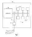
- FIG. 7illustrates a schematic view of an embodiment of a central processing unit incorporating devices having an atomic layer deposited dielectric layer, according to various embodiments of the present subject matter.
- FIG. 8illustrates a schematic view of an embodiment of a DRAM memory device having an atomic layer deposited dielectric layer, according to various embodiments of the present subject matter.
- wafer and substrate used in the following descriptioninclude any structure having an exposed surface with which to form the integrated circuit (IC) structure of the present subject matter.
- substrateis understood to include semiconductor wafers.
- substrateis also used to refer to semiconductor structures during processing, and may include other layers that have been fabricated thereupon. Both wafer and substrate include doped and undoped semiconductors, epitaxial semiconductor layers supported by a base semiconductor or insulator, as well as other semiconductor structures well known to one skilled in the art.
- conductoris understood to include semiconductors, and the term insulator or dielectric is defined to include any material that is less electrically conductive than the materials referred to as conductors.
- horizontalas used in this application is defined as a plane parallel to the conventional plane or surface of a wafer or substrate, regardless of the orientation of the wafer or substrate.
- verticalrefers to a direction perpendicular to the horizontal as defined above. Prepositions, such as “on”, “side” (as in “sidewall”), “higher”, “lower”, “over” and “under” are defined with respect to the conventional plane or surface being on the top surface of the wafer or substrate, regardless of the orientation of the wafer or substrate.
- An embodiment for a method for forming a dielectric layerincludes forming a layer of metal on a substrate by atomic layer deposition and forming a layer of an oxide of the metal, by atomic layer deposition, on the layer of metal.
- a layer of hafniumis formed on a substrate by atomic layer deposition, and a layer of hafnium oxide is formed on the hafnium by atomic layer deposition.
- the layer of hafniumis formed using at most ten atomic layer deposition cycles.
- the number of atomic layer deposition cycles to form the layer of hafniumranges from about four cycles to about ten cycles.
- a dielectric layer containing hafnium oxidehas a larger dielectric constant than silicon dioxide, a relatively small leakage current, and good stability with respect to a silicon based substrate.
- Such dielectric layersprovide a significantly thinner equivalent oxide thickness compared with a silicon oxide layer having the same physical thickness. Alternately, such dielectric layers provide a significantly thicker physical thickness than a silicon oxide layer having the same equivalent oxide thickness.
- Embodimentsinclude structures for capacitors, transistors, memory devices, and electronic systems with dielectric layers containing atomic layer deposited hafnium oxide, and methods for forming such structures.
- a gate dielectric 140 of FIG. 1Awhen operating in a transistor, has both a physical gate dielectric thickness and an equivalent oxide thickness (t eq ).
- the equivalent oxide thicknessquantifies the electrical properties, such as capacitance, of a gate dielectric 140 in terms of a representative physical thickness.
- the equivalent oxide thickness, t eqis defined as the thickness of a theoretical SiO 2 layer that would have the same capacitance density as a given dielectric, ignoring leakage current and reliability considerations.
- a SiO 2 layer of thickness, t, deposited on a Si surface as a gate dielectricwill have a t eq larger than its thickness, t.
- This t eqresults from the capacitance in the surface channel on which the SiO 2 is deposited due to the formation of a depletion/inversion region.
- This depletion/inversion regionmay result in t eq being from 3 to 6 Angstroms ( ⁇ ) larger than the SiO 2 thickness, t.
- the physical thickness for a SiO 2 layer used for a gate dielectricwould be need to be approximately 4 to 7 ⁇ .
- SiO 2 layerAdditional characteristics depend on the gate electrode used in conjunction with the SiO 2 gate dielectric. Using a conventional polysilicon gate results in an additional increase in t eq for the SiO 2 layer. This additional thickness could be eliminated by using a metal gate electrode, though metal gates are not currently used in typical complementary metal-oxide-semiconductor field effect transistor (CMOS) technology. Thus, future devices would be designed towards a physical SiO 2 gate dielectric layer of about 5 ⁇ or less. Such a small thickness for a SiO 2 oxide layer creates additional problems.
- CMOScomplementary metal-oxide-semiconductor field effect transistor
- Silicon dioxideis used as a gate dielectric, in part, due to its electrical isolation properties in a SiO 2 —Si based structure. This electrical isolation is due to the relatively large band gap of SiO 2 (8.9 eV) making it a good insulator from electrical conduction. Signification reductions in its band gap would eliminate it as a material for a gate dielectric. As the thickness of a SiO 2 layer decreases, the number of atomic layers, or monolayers of the SiO 2 decreases. At a certain thickness, the number of monolayers will be sufficiently small that the SiO 2 layer will not have a complete arrangement of atoms as in a larger or bulk layer.
- a thin SiO 2 layer of only one or two monolayerswill not form a full band gap.
- the lack of a full band gap in a SiO 2 gate dielectriccould cause an effective short between an underlying Si channel and an overlying polysilicon gate.
- This undesirable propertysets a limit on the physical thickness to which a SiO 2 layer may be scaled.
- the minimum thickness due to this monolayer effectis thought to be about 7–8 ⁇ . Therefore, for future devices to have a t eq less than about 10 ⁇ , dielectrics other than SiO 2 need to be considered for use as a gate dielectric.
- materials with a dielectric constant greater than that of SiO 2 , 3.9will have a physical thickness that may be considerably larger than a desired t eq , while providing the desired equivalent oxide thickness.
- an alternate dielectric material with a dielectric constant of 10could have a thickness of about 25.6 ⁇ to provide a t eq of 10 ⁇ , not including any depletion/inversion layer effects.
- a reduced equivalent oxide thickness for transistorsmay be realized by using dielectric materials with higher dielectric constants than SiO 2 .
- the thinner equivalent oxide thickness for lower transistor operating voltages and smaller transistor dimensionsmay be realized by a significant number of materials, but additional fabricating characteristics makes determining a suitable replacement for SiO 2 difficult.
- the current view for the microelectronics industryis still for Si based devices.
- the gate dielectric employedwill grow on a silicon substrate or silicon layer, which places significant restraints on the substitute dielectric material.
- a small layer of SiO 2could be formed in addition to the desired dielectric.
- the resultwould effectively be a dielectric layer consisting of two sublayers in parallel with each other and the silicon layer on which the dielectric is formed. In such a case, the resulting capacitance would be that of two dielectrics in series.
- the t eqis again limited by a SiO 2 layer.
- the t eqwould be limited by the layer with the lowest dielectric constant.
- the layer interfacing with the silicon layermust provide a high quality interface to maintain a high channel carrier mobility.
- One of the advantages for using SiO 2 as a gate dielectrichas been that the formation of the SiO 2 layer results in an amorphous gate dielectric. Having an amorphous structure for a gate dielectric is advantageous because grain boundaries in polycrystalline gate dielectrics provide high leakage paths. Additionally, grain size and orientation changes throughout a polycrystalline gate dielectric may cause variations in the layer's dielectric constant. Many materials having a high dielectric constant relative to SiO 2 also have a disadvantage of a crystalline form, at least in a bulk configuration. Thus, the best candidates for replacing SiO 2 as a gate dielectric are those with high dielectric constant and are able to be fabricated as a thin layer with an amorphous form.
- hafnium oxide, HfO 2with a bulk dielectric constant of about 25, appears to be a candidate for replacing SiO 2 .
- other considerations for selecting the material and method for forming a dielectric layer for use in electronic devices and systemsconcern the suitability of the material for applications requiring that the dielectric layer have an ultra-thin equivalent oxide thickness, form conformally on a substrate, and/or be engineered to specific thickness and elemental concentrations.
- Another considerationconcerns the roughness of the dielectric layer on a substrate. Surface roughness of the dielectric layer has a significant effect on the electrical properties of the gate oxide, and the resulting operating characteristics of the transistor. Leakage current through a physical 1.0 nm gate oxide has been found to be increased by a factor of 10 for every 0.1 increase in the root-mean-square (RMS) roughness.
- RMSroot-mean-square
- particles of the material to be depositedbombard the surface at a high energy. When a particle hits the surface, some particles adhere, and other particles cause damage. High-energy impacts remove body region particles creating pits.
- the surface of such a deposited layermay have a rough contour due to the rough interface at the body region.
- a hafnium oxide dielectric layer having a substantially smooth surface relative to other processing techniquesis formed using atomic layer deposition (ALD). Further, forming a dielectric layer using atomic layer deposition provides for controlling transitions between material layers. Thus, atomic layer deposited hafnium oxide dielectric layers may have an engineered transition with a substrate surface that has a substantially reduced or no interfacial SiO 2 layer. Further, the ALD deposited hafnium oxide dielectric layers provide conformal coverage on the surfaces on which they are deposited.
- ALDalso known as atomic layer epitaxy (ALE)
- ALEatomic layer epitaxy
- CVDchemical vapor deposition
- ALDgaseous precursors are introduced one at a time to the substrate surface mounted within a reaction chamber (or reactor). This introduction of the gaseous precursors takes the form of pulses of each gaseous precursor. Between the pulses, the reaction chamber is purged with a gas, which in many cases is an inert gas, and/or evacuated.
- CS-ALDchemisorption-saturated ALD
- the second pulsing phaseintroduces another precursor on the substrate where the growth reaction of the desired layer takes place. Subsequent to the layer growth reaction, reaction by-products and precursor excess are purged from the reaction chamber.
- one ALD cyclemay be performed in less than one second in properly designed flow type reaction chambers. Typically, precursor pulse times range from about 0.5 sec to about 2 to 3 seconds.
- ALDIn ALD, the saturation of all the reaction and purging phases makes the growth self-limiting. This self-limiting growth results in large area uniformity and conformality, which has important applications for such cases as planar substrates, deep trenches, and in the processing of porous silicon and high surface area silica and alumina powders.
- ALDprovides for controlling layer thickness in a straightforward manner by controlling the number of growth cycles.
- ALDwas originally developed to manufacture luminescent and dielectric layers needed in electroluminescent displays. Significant efforts have been made to apply ALD to the growth of doped zinc sulfide and alkaline earth metal sulfide layers. Additionally, ALD has been studied for the growth of different epitaxial II-V and II-VI layers, nonepitaxial crystalline or amorphous oxide and nitride layers and multilayer structures of these. There also has been considerable interest towards the ALD growth of silicon and germanium layers, but due to the difficult precursor chemistry, this has not been very successful.
- the precursors used in an ALD processmay be gaseous, liquid or solid. However, liquid or solid precursors must be volatile. The vapor pressure must be high enough for effective mass transportation. Also, solid and some liquid precursors need to be heated inside the reaction chamber and introduced through heated tubes to the substrates. The necessary vapor pressure must be reached at a temperature below the substrate temperature to avoid the condensation of the precursors on the substrate. Due to the self-limiting growth mechanisms of ALD, relatively low vapor pressure solid precursors may be used though evaporation rates may somewhat vary during the process because of changes in their surface area.
- precursors used in ALDthere are several other characteristics for precursors used in ALD.
- the precursorsmust be thermally stable at the substrate temperature because their decomposition would destroy the surface control and accordingly the advantages of the ALD method that relies on the reaction of the precursor at the substrate surface.
- the precursorshave to chemisorb on or react with the surface, though the interaction between the precursor and the surface as well as the mechanism for the adsorption is different for different precursors.
- the molecules at the substrate surfacemust react aggressively with the second precursor to form the desired solid layer. Additionally, precursors should not react with the layer to cause etching, and precursors should not dissolve in the layer. Using highly reactive precursors in ALD contrasts with the selection of precursors for conventional CVD.
- the by-products in the reactionmust be gaseous in order to allow their easy removal from the reaction chamber. Further, the by-products should not react or adsorb on the surface.
- RS-ALDreaction sequence ALD
- the self-limiting process sequenceinvolves sequential surface chemical reactions.
- RS-ALDrelies on chemistry between a reactive surface and a reactive molecular precursor.
- molecular precursorsare pulsed into the ALD reaction chamber separately.
- the metal precursor reaction at the substrateis typically followed by an inert gas pulse to remove excess precursor and by-products from the reaction chamber prior to pulsing the next precursor of the fabrication sequence.
- RS-ALDlayers can be layered in equal metered sequences that are all identical in chemical kinetics, deposition per cycle, composition, and thickness.
- RS-ALD sequencesgenerally deposit less than a full layer per cycle.
- a deposition or growth rate of about 0.25 to about 2.00 ⁇ per RS-ALD cyclemay be realized.
- RS-ALDThe characteristics of RS-ALD include continuity at an interface, conformality over a substrate, use of low temperature and mildly oxidizing processes, freedom from first wafer effects and chamber dependence, growth thickness dependent solely on the number of cycles performed, and ability to engineer multilayer laminate layers with resolution of one to two monolayers.
- RS-ALDallows for deposition control on the order on monolayers and the ability to deposit monolayers of amorphous layers.
- a sequencerefers to the ALD material formation based on an ALD reaction of a precursor or a precursor with its reactant precursor.
- forming a metal layer from a precursor containing the metalforms an embodiment of a metal sequence.
- forming a layer of metal oxide from a precursor containing the metal and from an oxygen containing precursor as its reactant precursorforms an embodiment of a metal/oxygen sequence, which may be referred to as the metal oxide sequence.
- a cycle of the metal sequenceincludes pulsing a precursor containing the metal and pulsing a purging gas for the precursor.
- a cycle of the metal oxide sequenceincludes pulsing a precursor containing the metal, pulsing a purging gas for the precursor, pulsing a reactant precursor, and pulsing a purging gas for the reactant precursor.
- a layer of hafnium oxideis formed on a substrate mounted in a reaction chamber by ALD using precursor gases individually pulsed into the reaction chamber.
- solid or liquid precursorsmay be used in an appropriately designed reaction chamber.
- ALD formation of other materialsis disclosed in co-pending, commonly assigned U.S. patent application: entitled “Atomic Layer Deposition and Conversion,” attorney docket no. 303.802US1, Ser. No. 10/137,058, and “Methods, Systems, and Apparatus for Atomic-Layer Deposition of Aluminum Oxides in Integrated Circuits,” attorney docket no. 1303.048US1, Ser. No. 10/137,168.
- FIG. 2Ashows an embodiment of an atomic layer deposition system 200 for processing a dielectric layer containing hafnium oxide.
- the elements depictedare those elements necessary for discussion of embodiments of the present subject matter such that those skilled in the art may practice various embodiments of the present subject matter without undue experimentation.
- a further discussion of the ALD reaction chambercan be found in co-pending, commonly assigned U.S. patent application: entitled “Methods, Systems, and Apparatus for Uniform Chemical-Vapor Depositions,” attorney docket no. 303.717US1, Ser. No. 09/797,324, incorporated herein by reference.
- a substrate 210is located inside a reaction chamber 220 of ALD system 200 . Also located within reaction chamber 220 is a heating element 230 , which is thermally coupled to substrate 210 to control the substrate temperature.
- a gas-distribution fixture 240introduces precursor gases to the substrate 210 .
- Each precursor gasoriginates from individual gas sources 251 – 254 whose flow is controlled by mass-flow controllers 256 – 259 , respectively.
- Each gas source, 251 – 254provides a precursor gas either by storing the precursor as a gas or by providing a location and apparatus for evaporating a solid or liquid material to form the selected precursor gas.
- additional gas sourcesmay be included, one for each metal precursor employed and one for each reactant precursor associated with each metal precursor.
- purging gas sources 261 , 262are also included in the ALD system, each of which is coupled to mass-flow controllers 266 , 267 , respectively. Furthermore, additional purging gas sources may be constructed in ALD system 200 , one purging gas source for each precursor gas. For a process that uses the same purging gas for multiple precursor gases less purging gas sources are used in ALD system 200 .
- Gas sources 251 – 254 and purging gas sources 261 – 262are coupled by their associated mass-flow controllers to a common gas line or conduit 270 , which is coupled to the gas-distribution fixture 240 inside reaction chamber 220 .
- Gas conduit 270is also coupled to vacuum pump, or exhaust pump, 281 by mass-flow controller 286 to remove excess precursor gases, purging gases, and by-product gases at the end of a purging sequence from gas conduit 270 .
- Vacuum pump, or exhaust pump, 282is coupled by mass-flow controller 287 to remove excess precursor gases, purging gases, and by-product gases at the end of a purging sequence from reaction chamber 220 .
- mass-flow controller 287to remove excess precursor gases, purging gases, and by-product gases at the end of a purging sequence from reaction chamber 220 .
- control displays, mounting apparatus, temperature sensing devices, substrate maneuvering apparatus, and necessary electrical connections as are known to those skilled in the artare not shown in FIG. 2A .
- FIG. 2Bshows an embodiment of a gas-distribution fixture 240 of atomic layer deposition system 200 for processing a dielectric layer containing hafnium oxide.
- Gas-distribution fixture 240includes a gas-distribution member 242 , and a gas inlet 244 .
- Gas inlet 244couples gas-distribution member 242 to gas conduit 270 of FIG. 2A .
- Gas-distribution member 242includes gas-distribution holes, or orifices, 246 and gas-distribution channels 248 .
- holes 246are substantially circular with a common diameter in the range of 15–20 microns
- gas-distribution channels 248have a common width in the range of 20–45 microns.
- the surface 249 of gas distribution member 242 having gas-distribution holes 246is substantially planar and parallel to substrate 210 of FIG. 2A .
- other embodimentsuse other surface forms as well as shapes and sizes of holes and channels. The distribution and size of holes may also affect deposition thickness and thus might be used to assist thickness control.
- Holes 246are coupled through gas-distribution channels 248 to gas inlet 244 .
- ALD system 200is well suited for practicing the present subject matter, other ALD systems commercially available may be used.
- ALD system 200may be controlled by a computer. To focus on the use of ALD system 200 in the various embodiments of the present subject matter, the computer is not shown. Those skilled in the art can appreciate that the individual elements such as pressure control, temperature control, and gas flow within ALD system 200 may be under computer control.
- a computerexecutes instructions stored in a computer readable medium to accurately control the integrated functioning of the elements of ALD system 200 to form a dielectric layer.
- FIG. 3illustrates a flow diagram of elements for an embodiment of a method to process a dielectric layer by atomic layer deposition.
- FIG. 1Bshows an embodiment of a stage of forming gate dielectric layer 140 of transistor 100 according to an embodiment.
- the elements of FIG. 3are not limited to forming a gate dielectric of a transistor.
- This embodimentincludes forming a layer of a metal 141 on a substrate by atomic layer deposition, at block 310 , and forming on the layer of metal 141 , by atomic layer deposition, a layer of an oxide of the metal 143 at block 320 .
- the layer of metal 141is formed through performing at most ten cycles of the metal sequence.
- the layer of metal 141is formed through performing from four cycles to ten cycles of the metal sequence. The number of cycles for the metal oxide sequence to be performed is selected to provide a desired thickness of the metal oxide 140 .
- a hafnium layeris formed on a substrate by atomic layer deposition.
- the hafniumis deposited on the substrate using a hafnium nitrate precursor.
- at most ten cyclesare performed using the hafnium nitrate precursor.
- a predetermined number of cycles of a hafnium oxide sequenceare performed.
- a hafnium oxide layer on the substrateresults.
- a Hf/HfO 2 nanolaminateis fabricated.
- oxygen diffusing towards the silicon substrate during the HfO 2 formationinteracts with the hafnium layer that prevents formation of a silicon oxide interfacial region.
- Performing each atomic layer depositionincludes pulsing one or more precursors into a reaction chamber for a predetermined period.
- the predetermined periodis individually controlled for each precursor pulsed into the reaction chamber.
- the substrateis maintained at a selected temperature for each pulsing of a precursor, where the selected temperature is set independently for pulsing each precursor.
- each precursormay be pulsed into the reaction under separate environmental conditions. Appropriate temperatures and pressures are maintained dependent on the nature of the precursor, whether the precursor is a single precursor or a mixture of precursors.
- the pulsing of the precursor gasesis separated by purging the reaction chamber with a purging gas following each pulsing of a precursor.
- nitrogen gasis used as the purging gas following the pulsing of each precursor used in a cycle to form a layer of hafnium oxide.
- the reaction chambermay also be purged by evacuating the reaction chamber.
- FIG. 4illustrates a flow diagram of elements for an embodiment of a method to process a dielectric layer containing hafnium oxide by atomic layer deposition. This embodiment may be implemented with the atomic layer deposition system 200 of FIG. 2A , B.
- substrate 210is prepared.
- the substrate used for forming a transistoris typically a silicon or silicon containing material. In other embodiments, germanium, gallium arsenide, silicon-on-sapphire substrates, or other suitable substrates may be used.
- This preparation processmay include cleaning of substrate 210 and forming layers and regions of the substrate, such as drains and sources of a metal oxide semiconductor (MOS) transistor, prior to forming a gate dielectric.
- MOSmetal oxide semiconductor
- the substrateis cleaned to provide an initial substrate depleted of its native oxide.
- the initial substrateis cleaned to also provide a hydrogen-terminated surface.
- a silicon substrateundergoes a final HF rinse prior to ALD processing to provide the silicon substrate with a hydrogen-terminated surface without a native silicon oxide layer.
- the sequencing of the formation of the regions of the transistor being processedfollows typical sequencing that is generally performed in the fabrication of a MOS transistor as is well known to those skilled in the art. Included in the processing is the masking of substrate regions to be protected during the gate dielectric formation, as is typically performed in MOS fabrication. In this embodiment, the unmasked region may include a body region of a transistor; however one skilled in the art will recognize that other semiconductor device structures may utilize this process. Additionally, substrate 210 in its ready for processing form is conveyed into a position in reaction chamber 220 for ALD processing.
- a hafnium containing precursoris pulsed into reaction chamber 220 .
- anhydrous hafnium nitrate, Hf(NO 3 ) 4is used as a precursor.
- the Hf(NO 3 ) 4 precursoris pulsed into reaction chamber 220 through the gas-distribution fixture 240 on substrate 210 .
- Mass-flow controller 256regulates the flow of the Hf(NO 3 ) 4 from gas source 251 .
- the substrate temperatureis maintained at about 180° C. In another embodiment, the substrate temperature is maintained between about 300° C. and about 500° C.
- the Hf(NO 3 ) 4reacts with the surface of the substrate 210 in the desired region defined by the unmasked areas of the substrate 210 .
- a hafnium containing precursorincludes a hafnium-tetrachloride precursor.
- hafnium-tetrachloride precursorsAlthough excellent uniformity and initiation of deposition is provided with hafnium-tetrachloride precursors, a number of ALD cycles are used to produce total coverage of a hydrogen-terminated silicon surface since the displacement of Si—H bonds with the tetrachloride species is not easily achieved. This difficulty related to initiation of deposition on hydrogen-terminated silicon can lead to surface roughness and deposition inconsistencies. Moreover, the metal tetrachloride also has a tendency to incorporate trace amounts of chlorine in a layer, which can lead to stability and reliability problems.
- Anhydrous nitrates of hafniumallows for better control of the initiation of the deposition on hydrogen-terminated silicon , which aids in optimizing the interface properties and improvement of the carrier mobility in transistors. These precursors do not leave hydrocarbons or halogen impurities, and the nitrogen oxide by-products are easily removed.
- a first purging gasis pulsed into reaction chamber 220 .
- nitrogenwith a purity of about 99.999% is used as a purging gas.
- Mass-flow controller 266regulates the nitrogen flow from the purging gas source 261 into the gas conduit 270 . Using the pure nitrogen purge avoids overlap of the precursor pulses and possible gas phase reactions.
- a cycle of the hafnium metal sequenceis completed.
- a determinationis made as to whether the desired number of hafnium metal cycles has been performed, at block 420 . If the desired number of cycles for the hafnium metal sequence has not been completed, the process returns to pulsing the hafnium containing precursor onto the substrate, at block 410 . If the desired number of cycles for the hafnium metal sequence had been completed, the process moves to forming a hafnium oxide on the hafnium layer.
- the desired number of cycles for the hafnium metal sequenceis a number of cycles to form a hafnium metal layer across the substrate providing a thickness of a few angstroms. In an embodiment, performing about four to ten cycles provides a few angstroms thickness. In another embodiment, performing about ten cycles provides the hafnium metal thickness. In an embodiment, each cycle for the hafnium sequence includes pulsing the hafnium nitrate for about 0.6 s, and pulsing the nitrogen purging gas for about 0.6 s. Forming the hafnium metal layer on the substrate prior to forming a hafnium oxide prevents oxygen from diffusing to the silicon surface during subsequent ALD formation of the hafnium oxide. As the hafnium oxide is being formed by ALD, oxygen that diffuses towards the silicon substrate interacts with the hafnium metal layer. In an embodiment, the hafnium layer substantially becomes hafnium oxide.
- a second hafnium containing precursoris pulsed onto substrate 210 , at block 430 .
- anhydrous hafnium nitrate, Hf(NO 3 ) 4is used as a precursor.
- the Hf(NO 3 ) 4 precursoris pulsed into reaction chamber 220 through the gas-distribution fixture 240 on substrate 210 .
- Mass-flow controller 257regulates the flow of the Hf(NO 3 ) 4 from gas source 252 .
- the substrate temperatureis maintained at about 180° C. In another embodiment, the substrate temperature is maintained between about 300° C. and about 500° C.
- the Hf(NO 3 ) 4reacts with at the surface of substrate 210 on which the hafnium metal layer was formed in the desired region defined by the unmasked areas of the substrate 210 .
- a second purging gasis pulsed, at block, 435 .
- nitrogenis used as the second purging gas.
- Excess precursor gas, and reaction by-productsare removed from the system by the purge gas in conjunction with the exhausting of reaction chamber 220 using vacuum pump 282 through mass-flow controller 287 , and exhausting of the gas conduit 270 by the vacuum pump 281 through mass-flow controller 286 .
- an oxygen containing precursoris pulsed into reaction chamber 220 , at block 440 .
- the oxygen containing precursoris water vapor.
- the H 2 O vapor precursoris pulsed into reaction chamber 220 through the gas-distribution fixture 240 on substrate 210 .
- Mass-flow controller 258regulates the flow of the H 2 O vapor from gas source 253 .
- the substrate temperatureis maintained at about 180° C. In another embodiment, the substrate temperature is maintained between about 300° C. and about 500° C. The water vapor aggressively reacts at the current surface of substrate 210 .
- a third purging gasis introduced into the system.
- Nitrogen gasmay also be used as a purging and carrier gas.
- the nitrogen flowis controlled by mass-flow controller 267 from the purging gas source 262 into the gas conduit 270 and subsequently into reaction chamber 220 .
- argon gasmay be used as the purging gas.
- the substrateis held between at about 180° C. by the heating element 230 .
- the Hf(NO 3 ) 4is pulsed for about 0.6 s.
- the hafnium oxide sequencecontinues with a purge pulse followed by a water vapor pulse followed by a purge pulse.
- the hafnium/oxygen sequenceincludes a 0.6 s Hf(NO 3 ) 4 pulse, a 0.6 s nitrogen pulse, a 0.6 s water vapor pulse, and a 0.6 s nitrogen pulse.
- Other embodimentsinclude pulse periods that range from about 0.2 s to several seconds for the precursors and pulse periods that range from about 0.5 s to about 20 s for purging gases.
- the predetermined numbercorresponds to a predetermined thickness for the ALD hafnium oxide dielectric layer. If the number of completed cycles is less than the predetermined number, the second hafnium containing precursor is pulsed into reaction chamber 220 , at block 430 , and the process continues. If the total number of cycles to form the desired thickness has been completed, the dielectric layer containing hafnium oxide may be annealed to remove any residual nitrous oxide. To avoid the diffusion of oxygen during annealing to the semiconductor substrate surface, any annealing may be performed in an oxygen-free environment for short periods of time.
- An embodiment of an annealing environmentmay include a nitrogen atmosphere.
- the relatively low temperatures employed by atomic layer deposition of a hafnium oxide dielectric layerallows for the formation of an amorphous hafnium oxide dielectric layer.
- the thickness of a hafnium oxide layeris determined by a fixed growth rate for the pulsing periods and precursors used, set at a value such as N nm/cycle.
- tfor a desired hafnium oxide layer thickness, t, in an application such as forming a gate dielectric of a MOS transistor, the ALD process is repeated for t/N total cycles. Once the t/N cycles have completed, no further ALD processing for hafnium oxide is performed.
- ALD processingprovides for the engineering of a dielectric layer containing hafnium oxide having a dielectric constant in the range from about 8 to about 25.
- processing the device having the dielectric layer containing hafnium oxideis completed.
- completing the deviceincludes completing the formation of a transistor.
- completing the deviceincludes completing the formation of a capacitor.
- completing the processincludes completing the construction of a memory device having an array with access transistors formed with gate dielectrics containing atomic layer deposited hafnium oxide.
- completing the processincludes the formation of an electronic system including an information handling device that uses electronic devices with transistors formed with dielectric layers containing atomic layer deposited hafnium oxide.
- information handling devicessuch as computers include many memory devices, having many access transistors.
- the elements of a method for forming an atomic layer deposited hafnium oxide layer in the embodiment of FIG. 4may be performed under various other environmental conditions and pulse periods depending on the hafnium oxide layer to be formed for a given application and the system used to fabricate the hafnium oxide layer. Determination of the environmental conditions, precursors used, purging gases employed, and pulse periods for the precursors and purging gases may be made without undue experimentation.
- Atomic layer deposition of a hafnium oxide dielectric layermay be processed in an atomic layer deposition system such as ALD system 200 under computer control to perform various embodiments, and operated under computer-executable instructions to perform these embodiments.
- a computerized method and the computer-executable instructions for a method for forming a dielectric layerincludes forming a layer of metal by atomic layer deposition, and forming on the layer of metal, by atomic layer deposition, a layer of an oxide of the metal.
- a computerized method and the computer-executable instructions for a method for forming a dielectric layerinclude depositing a layer of hafnium by atomic layer deposition on a substrate surface by atomic layer deposition, and forming a layer of hafnium oxide, by atomic layer deposition, on the layer of hafnium metal.
- a computerized method and the computer-executable instructions for a method for forming a dielectric layerfurther includes forming the hafnium oxide dielectric layer by atomic layer deposition, where each precursor is pulsed into a reaction chamber for a predetermined period.
- the predetermined periodis individually controlled for each precursor pulsed into the reaction chamber.
- the substratemay be maintained at a selected temperature for each pulsing of a precursor, where the selected temperature is set independently for pulsing each precursor.
- each pulsing of a precursoris followed by purging the reaction chamber with a purging gas.
- a computerized method and the computer-executable instructions for a method for forming a dielectric layermay includes regulating the deposition of hafnium and hafnium oxide to form a dielectric layer having a dielectric constant in the range from about 8 to about 25.
- a computerized method and the computer-executable instructions for a method for forming a dielectric layerinclude controlling an environment of a reaction chamber. Additionally, the computerized method controls the pulsing of purging gases, one for each precursor gas and pulsing each purging gas after pulsing the associated precursor gas. Using a computer to control parameters for growing the dielectric layer provides for processing the dielectric layer over a wide range of parameters allowing for the determination of an optimum parameter set for the ALD system used.
- the computer-executable instructionsmay be provided in any computer-readable medium. Such computer-readable medium may include, but is not limited to, floppy disks, diskettes, hard disks, CD-ROMS, flash ROMS, nonvolatile ROM, and RAM.
- An embodiment of this methodmay be realized using ALD system 200 of FIG. 2A , where the controls for the individual elements of ALD system 200 are coupled to a computer, not shown in FIG. 2A .
- the computerprovides control of the operation for processing a hafnium oxide dielectric layer by regulating the flow of precursor gases into reaction chamber 220 .
- the computercontrols the flow rate of precursor gases and the pulsing periods for these gases by controlling mass-flow controllers 256 – 259 . Additionally, the computer controls the temperature of gas sources 251 – 254 . Further, the pulse period and flow of purging gases from purging gas sources 261 , 262 is regulated through computer control of mass-flow controllers 266 , 267 , respectively.
- the computeralso regulates the environment of reactor chamber 220 in which a dielectric layer is being formed on substrate 210 .
- the computerregulates the pressure in reaction chamber 220 within a predetermined pressure range by controlling vacuum pumps 281 , 282 through mass-flow controllers 286 , 287 , respectively.
- the computeralso regulates the temperature range for substrate 210 within a predetermined range by controlling heater 230 .
- FIG. 2AFor convenience, the individual control lines to elements of ALD 200 , as well as a computer, are not shown in FIG. 2A .
- the above description of the computer control in conjunction with FIG. 2Aprovides information for those skilled in the art to practice embodiments for forming a dielectric layer containing hafnium oxide using a computerized method as described herein.
- t equseful equivalent oxide thickness
- the relatively large dielectric constant for material layers of hafnium oxideallows for the engineering of dielectric layers having a physical thickness in the 10 nm (100 ⁇ ) range, while achieving a t eq of less than 5 nm (50 ⁇ ). From above, it is apparent that a layer containing hafnium oxide may be attained with a t eq ranging from about 1.5 ⁇ to about 12 ⁇ . Further, an atomic layer deposited hafnium oxide layer may provide a t eq significantly less than 2 or 3 ⁇ , even less than 1.5 ⁇ .
- Attainment of a t eq in the monolayer thickness rangeis associated with an interfacial layer between a semiconductor substrate surface and the hafnium oxide dielectic layer that is exceptionally small or composed of a material having a dielectic constant approaching that of the hafnium oxide value.
- the formation of a SiO 2 interfacial layershould be avoided.
- the preparation of the semiconductor substrate surface prior to the first pulse of the first sequence of the ALD processshould include removing any SiO 2 layer that may exist and preventing the formation of a SiO 2 prior to the beginning of the ALD process.
- initial formation of a metal layer by ALDsuch as forming a hafnium layer in an embodiment for a hafnium oxide dielectric layer, assists in the reduction or elimination of a SiO 2 interfacial layer.
- ALDatomic layer deposition
- Forming the hafnium metal layer on the substrate prior to forming a hafnium oxideprevents oxygen from diffusing to the silicon surface during subsequent ALD formation of the hafnium oxide.
- oxygen that diffuses towards the silicon substrateinteracts with the hafnium metal layer.
- the hafnium layersubstantially becomes hafnium oxide.
- Hafnium metal at the interface with a silicon substratemay form a hafnium silicide as an interfacial layer between the silicon substrate and the hafnium oxide layer.
- This hafnium suicide interfacial layerthough small reduces the effective dielectric constant for the dielectric layer disposed on the silicon substrate.
- the dielectric constant for the hafnium silicideis about 8, which is significantly higher than a silicon dioxide dielectric layer.
- the dielectric constant for the hafnium oxide formed by atomic layer deposition of hafnium metal followed by atomic layer deposition of hafnium oxideranges from about 8 to about 25.
- any micro-roughness associated with thin layers of hafnium oxidemay be due to partial monolayer formation of the dielectric layer across the substrate surface. With some areas of the dielectric layer forming a monolayer in two or three cycles, while another area or region of the layer forms a monolayer in one or two cycles, the surface of the hafnium oxide dielectric layer may exhibit some micro-roughness. It is anticipated that the use of hafnium nitrate precursors assists in providing for uniform distribution across the substrate surface to help alleviate the occurrence of such micro-roughness of the dielectric layer.
- growth rates and processing conditions for providing a hafnium oxide dielectric layer with reduced or substantially eliminated micro-roughnessmay be determined during normal initial testing of the ALD system for processing a hafnium oxide dielectric layer for a given application without undue experimentation.
- dielectric layers of hafnium oxide formed by atomic layer depositionmay provide not only ultra thin t eq layers, but also layers with relatively low leakage current.
- ALD processingprovides for dielectric layers that provide conformal layering on selected substrate surfaces.
- Embodiments of processes described above for performing atomic layer deposition of hafnium oxideare used to precisely control the thickness of the dielectric layer formed, where, in addition to providing an ultra thin t eq , the atomic layer deposition process provides for relatively smooth surfaces and limited interfacial layer formation.
- these embodiments for ALD processing of dielectric layers, such as hafnium oxide dielectric layersmay be implemented to form transistors, capacitors, memory devices, and other electronic systems including electro-optic devices, microwave devices, and information handling devices. With careful preparation and engineering of the hafnium oxide layer, limiting the size of interfacial regions, a teq of about 5 ⁇ to about 3 ⁇ or lower for these devices is anticipated.
- a transistor 100 as depicted in FIG. 1Amay be formed by forming a source region 120 and a drain region 130 in a silicon based substrate 110 where source and drain regions 120 , 130 are separated by a body region 132 .
- Body region 132defines a channel having a channel length 134 .
- a dielectric layeris disposed on substrate 110 formed as a layer containing hafnium oxide on substrate 110 by atomic layer deposition. The resulting hafnium oxide dielectric layer forms gate dielectric 140 .
- a gate 150is formed over gate dielectric 140 .
- forming gate 150may include forming a polysilicon layer, though a metal gate may be formed in an alternative process.
- Forming the substrate, the source and drain regions, and the gateis performed using standard processes known to those skilled in the art. Additionally, the sequencing of the various elements of the process for forming a transistor is conducted with standard fabrication processes, also as known to those skilled in the art.
- the method for forming an atomic layer deposited hafnium oxide in various embodimentsmay be applied to other transistor structures having dielectric layers.
- FIG. 5shows an embodiment of a configuration of a transistor 500 having an atomic layer deposited hafnium oxide dielectric layer.
- Transistor 500includes a silicon based substrate 510 with a source 520 and a drain 530 separated by a body region 532 .
- Body region 532 between source 520 and drain 530defines a channel region having a channel length 534 .
- Located above body region 532is a stack 555 including a gate dielectric 540 , a floating gate 552 , a floating gate dielectric 542 , and a control gate 550 .
- Gate dielectric 540may be formed containing atomic layer deposited hafnium oxides described above with the remaining elements of the transistor 500 formed using processes known to those skilled in the art. Alternately, both gate dielectric 540 and floating gate dielectric 542 may be formed as dielectric layers containing hafnium oxide in various embodiments as described herein.
- a methodincludes forming a first conductive layer, forming a dielectric layer containing hafnium oxide on the first conductive layer by atomic layer deposition, and forming a second conductive layer on the dielectric layer.
- ALD formation of the hafnium oxide dielectric layerallows the dielectric layer to be engineered within a predetermined composition providing a desired dielectric constant.
- Transistors, capacitors, and other devices having dielectric layers, such as hafnium oxide dielectric layers, formed by atomic layer deposition using methods described hereinmay be implemented into memory devices and electronic systems including information handling devices.
- Such information devicesmay include wireless systems, telecommunication systems, and computers.
- An embodiment of a computer having a dielectric layer, such as a hafnium oxide dielectric layer, formed by atomic layer deposition using methods described hereinis shown in FIGS. 6–8 and described below. While specific types of memory devices and computing devices are shown below, it will be recognized by one skilled in the art that several types of memory devices and electronic systems including information handling devices utilize the present subject matter.
- a personal computer 600may include a monitor 601 , keyboard input 602 and a central processing unit 604 .
- Central processor unit 604typically may include microprocessor 706 , memory bus circuit 708 having a plurality of memory slots 712 ( a–n ), and other peripheral circuitry 710 .
- Peripheral circuitry 710permits various peripheral devices 724 to interface processor-memory bus 720 over input/output (I/O) bus 722 .
- the personal computer shown in FIGS. 6 and 7also includes at least one transistor having a dielectric layer, such as a hafnium oxide dielectric layer, formed by atomic layer deposition using methods described herein according an embodiment of the present subject matter.
- Microprocessor 706produces control and address signals to control the exchange of data between memory bus circuit 708 and microprocessor 706 and between memory bus circuit 708 and peripheral circuitry 710 . This exchange of data is accomplished over high speed memory bus 720 and over high speed I/O bus 722 .
- Coupled to memory bus 720are pluralities of memory slots 712 ( a– ), which receive memory devices well known to those skilled in the art.
- memory slots 712For example, single in-line memory modules (SIMMs) and dual in-line memory modules (DIMMs) may be used in the implementation of embodiment of the present subject matter.
- Page mode operations in a DRAMare defined by the method of accessing a row of a memory cell arrays and randomly accessing different columns of the array. Data stored at the row and column intersection may be read and output while that column is accessed. Page mode DRAMs use access steps, which limit the communication speed of memory circuit 708 .
- EDOextended data output
- DDR SDRAMDDR SDRAM
- SLDRAMDirect RDRAM
- otherssuch as SRAM or Flash memories.
- FIG. 8illustrates a schematic view of an embodiment of a DRAM memory device 800 having an atomic layer deposited dielectric layer formed according to an embodiment described herein.
- Illustrative DRAM memory device 800is compatible with memory slots 712 ( a–n ).
- the description of DRAM memory device 800has been simplified for purposes of illustrating a DRAM memory device and is not intended to be a complete description of all the features of a DRAM. Those skilled in the art will recognize that a wide variety of memory devices may be used in the implementation of embodiments of the present subject matter.
- the embodiment of a DRAM memory device shown in FIG. 8includes at least one transistor having a dielectric layer, such as a hafnium oxide dielectric layer, formed by atomic layer deposition using methods described herein according to the teachings of the present subject matter.
- Control, address and data information provided over memory bus 720is further represented by individual inputs to DRAM 800 , as shown in FIG. 8 . These individual representations are illustrated by data lines 802 , address lines 804 and various discrete lines directed to control logic 806 .
- DRAM 800includes memory array 810 , which in turn comprises rows and columns of addressable memory cells. Each memory cell in a row is coupled to a common word line. The word line is coupled to gates of individual transistors, where at least one transistor has a gate coupled to a gate dielectric, such as a hafnium oxide dielectric layer, formed by atomic layer deposition in accordance with the method and structure previously described above. Additionally, each memory cell in a column is coupled to a common bit line. Each cell in memory array 810 may include a storage capacitor and an access transistor as is conventional in the art.
- DRAM 800interfaces with, for example, microprocessor 706 through address lines 804 and data lines 802 .
- DRAM 800may interface with a DRAM controller, a micro-controller, a chip set or other electronic system.
- Microprocessor 706also provides a number of control signals to DRAM 800 , including but not limited to, row and column address strobe signals RAS and CAS, write enable signal WE, an output enable signal OE and other conventional control signals.
- Row address buffer 812 and row decoder 814receive and decode row addresses from row address signals provided on address lines 804 by microprocessor 706 . Each unique row address corresponds to a row of cells in memory array 810 .
- Row decoder 814may include a word line driver, an address decoder tree, and circuitry which translates a given row address received from row address buffers 812 and selectively activates the appropriate word line of memory array 810 via the word line drivers.
- Column address buffer 816 and column decoder 818receive and decode column address signals provided on address lines 804 .
- Column decoder 818also determines when a column is defective and the address of a replacement column.
- Column decoder 818is coupled to sense amplifiers 820 .
- Sense amplifiers 820are coupled to complementary pairs of bit lines of memory array 810 .
- Sense amplifiers 820are coupled to data-in buffer 822 and data-out buffer 824 .
- Data-in buffers 822 and data-out buffers 824are coupled to data lines 802 .
- data lines 802provide data to data-in buffer 822 .
- Sense amplifier 820receives data from data-in buffer 822 and stores the data in memory array 810 as a charge on a capacitor of a cell at an address specified on address lines 804 .
- DRAM 800transfers data to microprocessor 706 from memory array 810 .
- Complementary bit lines for the accessed cellare equilibrated during a precharge operation to a reference voltage provided by an equilibration circuit and a reference voltage supply.
- the charge stored in the accessed cellis then shared with the associated bit lines.
- a sense amplifier of sense amplifiers 820detects and amplifies a difference in voltage between the complementary bit lines.
- the sense amplifierpasses the amplified voltage to data-out buffer 824 .
- Control logic 806is used to control the many available functions of DRAM 800 .
- various control circuits and signals not detailed hereininitiate and synchronize DRAM 800 operation as known to those skilled in the art.
- the description of DRAM 800has been simplified for purposes of illustrating an embodiment of the present subject matter and is not intended to be a complete description of all the features of a DRAM.
- CMOScomplementary metal-oxide-semiconductor
- RDRAMsRDRAMs
- VRAMs and EEPROMsmay be used in the implementation of embodiments of the present subject matter.
- the DRAM implementation described hereinis illustrative only and not intended to be exclusive or limiting.
- a dielectric layersuch as a hafnium oxide dielectric layer, formed by atomic layer deposition using methods described herein produce a reliable dielectric layer having an equivalent oxide thickness thinner than attainable using SiO 2 .
- Dielectric layers containing atomic layer deposited hafnium oxide formed using the methods described hereinare thermodynamically stable such that the dielectric layers formed will have minimal reactions with a silicon substrate or other structures during processing.
- hafnium oxide layers by atomic layer deposition in relatively low processing temperaturesallows for hafnium oxide layers that are amorphous and conformally layered on a substrate surface. Further, the ALD formation of a hafnium oxide dielectric layer provides for enhanced dielectric and electrical properties relative to those attained with an amorphous SiO x layer. These properties of layers containing atomic layer deposited hafnium oxide layers allow for application as dielectric layers in numerous electronic devices and systems.
- Capacitors, transistors, electro-optic devices, higher level ICs or devices, and electronic systemsare constructed utilizing various embodiments of the process for forming a dielectric layer having an ultra thin equivalent oxide thickness, t eq .
- Gate dielectric layers or layers containing atomic layer deposited hafnium oxideare formed having a dielectric constant substantially higher than that of silicon oxide, where the dielectric layers are capable of a t eq thinner than 10 ⁇ , thinner than the expected limit for SiO 2 gate dielectrics.
- the thinner t eq of these dielectric layersallows for a higher capacitance than SiO 2 gate dielectrics, which provides further effective scaling for microelectronic devices and systems.
- the physical thickness of the atomic layer deposited hafnium oxide dielectric layeris much larger than the SiO 2 thickness associated with the t eq limit of SiO 2 . Forming the larger thickness aids in the manufacturing process for gate dielectrics and other dielectric layers. Further, a hafnium oxide layer processed in relatively low temperatures allowed by atomic layer deposition provides amorphous dielectric layers having relatively low leakage current for use as dielectric layers in electronic devices and systems.
Landscapes
- Engineering & Computer Science (AREA)
- Manufacturing & Machinery (AREA)
- Physics & Mathematics (AREA)
- Condensed Matter Physics & Semiconductors (AREA)
- General Physics & Mathematics (AREA)
- Computer Hardware Design (AREA)
- Microelectronics & Electronic Packaging (AREA)
- Power Engineering (AREA)
- Chemical & Material Sciences (AREA)
- Chemical Kinetics & Catalysis (AREA)
- Formation Of Insulating Films (AREA)
- Semiconductor Memories (AREA)
- Insulated Gate Type Field-Effect Transistor (AREA)
- Fixed Capacitors And Capacitor Manufacturing Machines (AREA)
- Non-Volatile Memory (AREA)
- Chemical Vapour Deposition (AREA)
- Semiconductor Integrated Circuits (AREA)
Abstract
Description
t=(κ/κox)teq=(κ/3.9)teq.
Thus, materials with a dielectric constant greater than that of SiO2, 3.9, will have a physical thickness that may be considerably larger than a desired teq, while providing the desired equivalent oxide thickness. For example, an alternate dielectric material with a dielectric constant of 10 could have a thickness of about 25.6 Å to provide a teqof 10 Å, not including any depletion/inversion layer effects. Thus, a reduced equivalent oxide thickness for transistors may be realized by using dielectric materials with higher dielectric constants than SiO2.
teq=tSiO2+(κox/κ)t.
Thus, if a SiO2layer is formed in the process, the teqis again limited by a SiO2layer. In the event that a barrier layer is formed between the silicon layer and the desired dielectric in which the barrier layer prevents the formation of a SiO2layer, the teqwould be limited by the layer with the lowest dielectric constant. However, whether a single dielectric layer with a high dielectric constant or a barrier layer with a higher dielectric constant than SiO2is employed, the layer interfacing with the silicon layer must provide a high quality interface to maintain a high channel carrier mobility.
| Physical | Physical | Physical | Physical | ||
| Thickness | Thickness | Thickness | Thickness | ||
| t = 1.0 nm | t = 2.5 nm | t = 5.0 nm | t = 10.0 nm | ||
| (10 Å) | (25 Å) | (50 Å) | (100 Å) | ||
| κ | teq(Å) | teq(Å) | teq(Å) | teq(Å) |
| 8 | 4.88 | 12.19 | 24.38 | 48.75 |
| 10 | 3.90 | 9.75 | 19.50 | 39.00 |
| 15 | 2.60 | 6.50 | 13.00 | 26.00 |
| 20 | 1.95 | 4.88 | 9.75 | 19.50 |
| 25 | 1.56 | 3.90 | 7.80 | 15.60 |
Claims (56)
Priority Applications (7)
| Application Number | Priority Date | Filing Date | Title |
|---|---|---|---|
| US10/379,470US7192892B2 (en) | 2003-03-04 | 2003-03-04 | Atomic layer deposited dielectric layers |
| JP2006509146AJP2006523952A (en) | 2003-03-04 | 2004-03-04 | Atomic layer insulating layer |
| EP04717434AEP1599899A2 (en) | 2003-03-04 | 2004-03-04 | Atomic layer deposited dielectric layers |
| KR1020057016560AKR100738731B1 (en) | 2003-03-04 | 2004-03-04 | Apparatus having a dielectric layer and methods of forming the apparatus having the dielectric layer |
| PCT/US2004/006685WO2004079796A2 (en) | 2003-03-04 | 2004-03-04 | Atomic layer deposited dielectric layers |
| CNB2004800121284ACN100530562C (en) | 2003-03-04 | 2004-03-04 | Atomic layer deposited dielectric layers |
| US11/213,013US7405454B2 (en) | 2003-03-04 | 2005-08-26 | Electronic apparatus with deposited dielectric layers |
Applications Claiming Priority (1)
| Application Number | Priority Date | Filing Date | Title |
|---|---|---|---|
| US10/379,470US7192892B2 (en) | 2003-03-04 | 2003-03-04 | Atomic layer deposited dielectric layers |
Related Child Applications (1)
| Application Number | Title | Priority Date | Filing Date |
|---|---|---|---|
| US11/213,013DivisionUS7405454B2 (en) | 2003-03-04 | 2005-08-26 | Electronic apparatus with deposited dielectric layers |
Publications (2)
| Publication Number | Publication Date |
|---|---|
| US20040175882A1 US20040175882A1 (en) | 2004-09-09 |
| US7192892B2true US7192892B2 (en) | 2007-03-20 |
Family
ID=32926684
Family Applications (2)
| Application Number | Title | Priority Date | Filing Date |
|---|---|---|---|
| US10/379,470Expired - Fee RelatedUS7192892B2 (en) | 2003-03-04 | 2003-03-04 | Atomic layer deposited dielectric layers |
| US11/213,013Expired - Fee RelatedUS7405454B2 (en) | 2003-03-04 | 2005-08-26 | Electronic apparatus with deposited dielectric layers |
Family Applications After (1)
| Application Number | Title | Priority Date | Filing Date |
|---|---|---|---|
| US11/213,013Expired - Fee RelatedUS7405454B2 (en) | 2003-03-04 | 2005-08-26 | Electronic apparatus with deposited dielectric layers |
Country Status (6)
| Country | Link |
|---|---|
| US (2) | US7192892B2 (en) |
| EP (1) | EP1599899A2 (en) |
| JP (1) | JP2006523952A (en) |
| KR (1) | KR100738731B1 (en) |
| CN (1) | CN100530562C (en) |
| WO (1) | WO2004079796A2 (en) |
Cited By (442)
| Publication number | Priority date | Publication date | Assignee | Title |
|---|---|---|---|---|
| US20050023625A1 (en)* | 2002-08-28 | 2005-02-03 | Micron Technology, Inc. | Atomic layer deposited HfSiON dielectric films |
| US20060115993A1 (en)* | 2002-09-10 | 2006-06-01 | Samsung Electronics Co., Ltd. | Post thermal treatment methods of forming high dielectric layers over interfacial layers in integrated circuit devices |
| US20060176645A1 (en)* | 2005-02-08 | 2006-08-10 | Micron Technology, Inc. | Atomic layer deposition of Dy doped HfO2 films as gate dielectrics |
| US20070092989A1 (en)* | 2005-08-04 | 2007-04-26 | Micron Technology, Inc. | Conductive nanoparticles |
| US7388246B2 (en) | 2002-08-29 | 2008-06-17 | Micron Technology, Inc. | Lanthanide doped TiOx dielectric films |
| US7390756B2 (en) | 2005-04-28 | 2008-06-24 | Micron Technology, Inc. | Atomic layer deposited zirconium silicon oxide films |
| US20080166867A1 (en)* | 2003-03-25 | 2008-07-10 | Rohm Co., Ltd. | Semiconductor device, method of manufacturing the same, and method of manufacturing metal compound thin film |
| US7402876B2 (en) | 2002-12-04 | 2008-07-22 | Micron Technology, Inc. | Zr— Sn—Ti—O films |
| US7405454B2 (en) | 2003-03-04 | 2008-07-29 | Micron Technology, Inc. | Electronic apparatus with deposited dielectric layers |
| US7410668B2 (en) | 2001-03-01 | 2008-08-12 | Micron Technology, Inc. | Methods, systems, and apparatus for uniform chemical-vapor depositions |
| US7410910B2 (en) | 2005-08-31 | 2008-08-12 | Micron Technology, Inc. | Lanthanum aluminum oxynitride dielectric films |
| US20080251836A1 (en)* | 2007-04-16 | 2008-10-16 | Hynix Semiconductor Inc. | Non-volatile memory device and method for fabricating the same |
| US20090101919A1 (en)* | 2007-10-11 | 2009-04-23 | Jie Yao | Photo-Detector Array, Semiconductor Image Intensifier And Methods Of Making And Using The Same |
| US7554161B2 (en) | 2002-06-05 | 2009-06-30 | Micron Technology, Inc. | HfAlO3 films for gate dielectrics |
| US20090173991A1 (en)* | 2005-08-04 | 2009-07-09 | Marsh Eugene P | Methods for forming rhodium-based charge traps and apparatus including rhodium-based charge traps |
| US7560395B2 (en) | 2005-01-05 | 2009-07-14 | Micron Technology, Inc. | Atomic layer deposited hafnium tantalum oxide dielectrics |
| US7560793B2 (en) | 2002-05-02 | 2009-07-14 | Micron Technology, Inc. | Atomic layer deposition and conversion |
| US7572695B2 (en) | 2005-05-27 | 2009-08-11 | Micron Technology, Inc. | Hafnium titanium oxide films |
| US7588988B2 (en) | 2004-08-31 | 2009-09-15 | Micron Technology, Inc. | Method of forming apparatus having oxide films formed using atomic layer deposition |
| US7601649B2 (en) | 2004-08-02 | 2009-10-13 | Micron Technology, Inc. | Zirconium-doped tantalum oxide films |
| US7611959B2 (en) | 2002-12-04 | 2009-11-03 | Micron Technology, Inc. | Zr-Sn-Ti-O films |
| US20090280648A1 (en)* | 2008-05-09 | 2009-11-12 | Cyprian Emeka Uzoh | Method and apparatus for 3d interconnect |
| US7625794B2 (en) | 2003-03-31 | 2009-12-01 | Micron Technology, Inc. | Methods of forming zirconium aluminum oxide |
| US7662729B2 (en) | 2005-04-28 | 2010-02-16 | Micron Technology, Inc. | Atomic layer deposition of a ruthenium layer to a lanthanide oxide dielectric layer |
| US7670646B2 (en) | 2002-05-02 | 2010-03-02 | Micron Technology, Inc. | Methods for atomic-layer deposition |
| US7709402B2 (en) | 2006-02-16 | 2010-05-04 | Micron Technology, Inc. | Conductive layers for hafnium silicon oxynitride films |
| US7719065B2 (en) | 2004-08-26 | 2010-05-18 | Micron Technology, Inc. | Ruthenium layer for a dielectric layer containing a lanthanide oxide |
| US20100123993A1 (en)* | 2008-02-13 | 2010-05-20 | Herzel Laor | Atomic layer deposition process for manufacture of battery electrodes, capacitors, resistors, and catalyzers |
| US20100258881A1 (en)* | 2009-04-14 | 2010-10-14 | International Business Machines Corporation | Dual metal and dual dielectric integration for metal high-k fets |
| US20100270626A1 (en)* | 2009-04-27 | 2010-10-28 | Raisanen Petri I | Atomic layer deposition of hafnium lanthanum oxides |
| US7867919B2 (en) | 2004-08-31 | 2011-01-11 | Micron Technology, Inc. | Method of fabricating an apparatus having a lanthanum-metal oxide dielectric layer |
| US7927948B2 (en) | 2005-07-20 | 2011-04-19 | Micron Technology, Inc. | Devices with nanocrystals and methods of formation |
| US8110469B2 (en) | 2005-08-30 | 2012-02-07 | Micron Technology, Inc. | Graded dielectric layers |
| US8253215B2 (en) | 2009-01-15 | 2012-08-28 | Wavefront Holdings, Llc | Mesa heterojunction phototransistor and method for making same |
| US8728832B2 (en) | 2012-05-07 | 2014-05-20 | Asm Ip Holdings B.V. | Semiconductor device dielectric interface layer |
| US8802201B2 (en) | 2009-08-14 | 2014-08-12 | Asm America, Inc. | Systems and methods for thin-film deposition of metal oxides using excited nitrogen-oxygen species |
| US8877655B2 (en) | 2010-05-07 | 2014-11-04 | Asm America, Inc. | Systems and methods for thin-film deposition of metal oxides using excited nitrogen-oxygen species |
| US8883270B2 (en) | 2009-08-14 | 2014-11-11 | Asm America, Inc. | Systems and methods for thin-film deposition of metal oxides using excited nitrogen—oxygen species |
| US8894870B2 (en) | 2013-02-01 | 2014-11-25 | Asm Ip Holding B.V. | Multi-step method and apparatus for etching compounds containing a metal |
| US8933375B2 (en) | 2012-06-27 | 2015-01-13 | Asm Ip Holding B.V. | Susceptor heater and method of heating a substrate |
| US8946830B2 (en) | 2012-04-04 | 2015-02-03 | Asm Ip Holdings B.V. | Metal oxide protective layer for a semiconductor device |
| US8986456B2 (en) | 2006-10-10 | 2015-03-24 | Asm America, Inc. | Precursor delivery system |
| US8993054B2 (en) | 2013-07-12 | 2015-03-31 | Asm Ip Holding B.V. | Method and system to reduce outgassing in a reaction chamber |
| US9005539B2 (en) | 2011-11-23 | 2015-04-14 | Asm Ip Holding B.V. | Chamber sealing member |
| US9018111B2 (en) | 2013-07-22 | 2015-04-28 | Asm Ip Holding B.V. | Semiconductor reaction chamber with plasma capabilities |
| US9017481B1 (en) | 2011-10-28 | 2015-04-28 | Asm America, Inc. | Process feed management for semiconductor substrate processing |
| US9021985B2 (en) | 2012-09-12 | 2015-05-05 | Asm Ip Holdings B.V. | Process gas management for an inductively-coupled plasma deposition reactor |
| US9029253B2 (en) | 2012-05-02 | 2015-05-12 | Asm Ip Holding B.V. | Phase-stabilized thin films, structures and devices including the thin films, and methods of forming same |
| US9087785B2 (en) | 2011-10-28 | 2015-07-21 | Taiwan Semiconductor Manufacturing Co., Ltd. | Method for fabricating oxides/semiconductor interfaces |
| US9096931B2 (en) | 2011-10-27 | 2015-08-04 | Asm America, Inc | Deposition valve assembly and method of heating the same |
| US9117866B2 (en) | 2012-07-31 | 2015-08-25 | Asm Ip Holding B.V. | Apparatus and method for calculating a wafer position in a processing chamber under process conditions |
| US9147737B2 (en) | 2012-09-03 | 2015-09-29 | Semiconductor Manufacturing International Corp. | Semiconductor device and fabrication method |
| US9167625B2 (en) | 2011-11-23 | 2015-10-20 | Asm Ip Holding B.V. | Radiation shielding for a substrate holder |
| US9169975B2 (en) | 2012-08-28 | 2015-10-27 | Asm Ip Holding B.V. | Systems and methods for mass flow controller verification |
| US9202727B2 (en) | 2012-03-02 | 2015-12-01 | ASM IP Holding | Susceptor heater shim |
| US9240412B2 (en) | 2013-09-27 | 2016-01-19 | Asm Ip Holding B.V. | Semiconductor structure and device and methods of forming same using selective epitaxial process |
| US9324811B2 (en) | 2012-09-26 | 2016-04-26 | Asm Ip Holding B.V. | Structures and devices including a tensile-stressed silicon arsenic layer and methods of forming same |
| US9341296B2 (en) | 2011-10-27 | 2016-05-17 | Asm America, Inc. | Heater jacket for a fluid line |
| US9394608B2 (en) | 2009-04-06 | 2016-07-19 | Asm America, Inc. | Semiconductor processing reactor and components thereof |
| US9396934B2 (en) | 2013-08-14 | 2016-07-19 | Asm Ip Holding B.V. | Methods of forming films including germanium tin and structures and devices including the films |
| US9404587B2 (en) | 2014-04-24 | 2016-08-02 | ASM IP Holding B.V | Lockout tagout for semiconductor vacuum valve |
| US9447498B2 (en) | 2014-03-18 | 2016-09-20 | Asm Ip Holding B.V. | Method for performing uniform processing in gas system-sharing multiple reaction chambers |
| US9455138B1 (en) | 2015-11-10 | 2016-09-27 | Asm Ip Holding B.V. | Method for forming dielectric film in trenches by PEALD using H-containing gas |
| US9458542B2 (en) | 2011-03-26 | 2016-10-04 | Honda Motor Co., Ltd. | Materials and design for an electrocatalytic device and method which produces carbon nanotubes and hydrocarbon transportation fuels |
| US9478415B2 (en) | 2015-02-13 | 2016-10-25 | Asm Ip Holding B.V. | Method for forming film having low resistance and shallow junction depth |
| US9484191B2 (en) | 2013-03-08 | 2016-11-01 | Asm Ip Holding B.V. | Pulsed remote plasma method and system |
| US9543180B2 (en) | 2014-08-01 | 2017-01-10 | Asm Ip Holding B.V. | Apparatus and method for transporting wafers between wafer carrier and process tool under vacuum |
| US9558931B2 (en) | 2012-07-27 | 2017-01-31 | Asm Ip Holding B.V. | System and method for gas-phase sulfur passivation of a semiconductor surface |
| US9556516B2 (en) | 2013-10-09 | 2017-01-31 | ASM IP Holding B.V | Method for forming Ti-containing film by PEALD using TDMAT or TDEAT |
| US9589770B2 (en) | 2013-03-08 | 2017-03-07 | Asm Ip Holding B.V. | Method and systems for in-situ formation of intermediate reactive species |
| US9605343B2 (en) | 2013-11-13 | 2017-03-28 | Asm Ip Holding B.V. | Method for forming conformal carbon films, structures conformal carbon film, and system of forming same |
| US9607837B1 (en) | 2015-12-21 | 2017-03-28 | Asm Ip Holding B.V. | Method for forming silicon oxide cap layer for solid state diffusion process |
| US9627221B1 (en) | 2015-12-28 | 2017-04-18 | Asm Ip Holding B.V. | Continuous process incorporating atomic layer etching |
| US9640416B2 (en) | 2012-12-26 | 2017-05-02 | Asm Ip Holding B.V. | Single-and dual-chamber module-attachable wafer-handling chamber |
| US9647114B2 (en) | 2015-08-14 | 2017-05-09 | Asm Ip Holding B.V. | Methods of forming highly p-type doped germanium tin films and structures and devices including the films |
| US9659799B2 (en) | 2012-08-28 | 2017-05-23 | Asm Ip Holding B.V. | Systems and methods for dynamic semiconductor process scheduling |
| US9657845B2 (en) | 2014-10-07 | 2017-05-23 | Asm Ip Holding B.V. | Variable conductance gas distribution apparatus and method |
| US9711345B2 (en) | 2015-08-25 | 2017-07-18 | Asm Ip Holding B.V. | Method for forming aluminum nitride-based film by PEALD |
| US9735024B2 (en) | 2015-12-28 | 2017-08-15 | Asm Ip Holding B.V. | Method of atomic layer etching using functional group-containing fluorocarbon |
| US9754779B1 (en) | 2016-02-19 | 2017-09-05 | Asm Ip Holding B.V. | Method for forming silicon nitride film selectively on sidewalls or flat surfaces of trenches |
| US9793115B2 (en) | 2013-08-14 | 2017-10-17 | Asm Ip Holding B.V. | Structures and devices including germanium-tin films and methods of forming same |
| US9793148B2 (en) | 2011-06-22 | 2017-10-17 | Asm Japan K.K. | Method for positioning wafers in multiple wafer transport |
| US9793135B1 (en) | 2016-07-14 | 2017-10-17 | ASM IP Holding B.V | Method of cyclic dry etching using etchant film |
| US9812320B1 (en) | 2016-07-28 | 2017-11-07 | Asm Ip Holding B.V. | Method and apparatus for filling a gap |
| US9859151B1 (en) | 2016-07-08 | 2018-01-02 | Asm Ip Holding B.V. | Selective film deposition method to form air gaps |
| US9887082B1 (en) | 2016-07-28 | 2018-02-06 | Asm Ip Holding B.V. | Method and apparatus for filling a gap |
| US9890456B2 (en) | 2014-08-21 | 2018-02-13 | Asm Ip Holding B.V. | Method and system for in situ formation of gas-phase compounds |
| US9891521B2 (en) | 2014-11-19 | 2018-02-13 | Asm Ip Holding B.V. | Method for depositing thin film |
| US9899291B2 (en) | 2015-07-13 | 2018-02-20 | Asm Ip Holding B.V. | Method for protecting layer by forming hydrocarbon-based extremely thin film |
| US9899405B2 (en) | 2014-12-22 | 2018-02-20 | Asm Ip Holding B.V. | Semiconductor device and manufacturing method thereof |
| US9905420B2 (en) | 2015-12-01 | 2018-02-27 | Asm Ip Holding B.V. | Methods of forming silicon germanium tin films and structures and devices including the films |
| US9909214B2 (en) | 2015-10-15 | 2018-03-06 | Asm Ip Holding B.V. | Method for depositing dielectric film in trenches by PEALD |
| US9916980B1 (en) | 2016-12-15 | 2018-03-13 | Asm Ip Holding B.V. | Method of forming a structure on a substrate |
| US9960072B2 (en) | 2015-09-29 | 2018-05-01 | Asm Ip Holding B.V. | Variable adjustment for precise matching of multiple chamber cavity housings |
| US10032628B2 (en) | 2016-05-02 | 2018-07-24 | Asm Ip Holding B.V. | Source/drain performance through conformal solid state doping |
| US10043661B2 (en) | 2015-07-13 | 2018-08-07 | Asm Ip Holding B.V. | Method for protecting layer by forming hydrocarbon-based extremely thin film |
| US10083836B2 (en) | 2015-07-24 | 2018-09-25 | Asm Ip Holding B.V. | Formation of boron-doped titanium metal films with high work function |
| US10090316B2 (en) | 2016-09-01 | 2018-10-02 | Asm Ip Holding B.V. | 3D stacked multilayer semiconductor memory using doped select transistor channel |
| US10087525B2 (en) | 2015-08-04 | 2018-10-02 | Asm Ip Holding B.V. | Variable gap hard stop design |
| US10087522B2 (en) | 2016-04-21 | 2018-10-02 | Asm Ip Holding B.V. | Deposition of metal borides |
| USD830981S1 (en) | 2017-04-07 | 2018-10-16 | Asm Ip Holding B.V. | Susceptor for semiconductor substrate processing apparatus |
| US10103040B1 (en) | 2017-03-31 | 2018-10-16 | Asm Ip Holding B.V. | Apparatus and method for manufacturing a semiconductor device |
| US10134757B2 (en) | 2016-11-07 | 2018-11-20 | Asm Ip Holding B.V. | Method of processing a substrate and a device manufactured by using the method |
| US10167557B2 (en) | 2014-03-18 | 2019-01-01 | Asm Ip Holding B.V. | Gas distribution system, reactor including the system, and methods of using the same |
| US10177025B2 (en) | 2016-07-28 | 2019-01-08 | Asm Ip Holding B.V. | Method and apparatus for filling a gap |
| US10179947B2 (en) | 2013-11-26 | 2019-01-15 | Asm Ip Holding B.V. | Method for forming conformal nitrided, oxidized, or carbonized dielectric film by atomic layer deposition |
| US10190213B2 (en) | 2016-04-21 | 2019-01-29 | Asm Ip Holding B.V. | Deposition of metal borides |
| US10211308B2 (en) | 2015-10-21 | 2019-02-19 | Asm Ip Holding B.V. | NbMC layers |
| US10229833B2 (en) | 2016-11-01 | 2019-03-12 | Asm Ip Holding B.V. | Methods for forming a transition metal nitride film on a substrate by atomic layer deposition and related semiconductor device structures |
| US10236177B1 (en) | 2017-08-22 | 2019-03-19 | ASM IP Holding B.V.. | Methods for depositing a doped germanium tin semiconductor and related semiconductor device structures |
| US10249577B2 (en) | 2016-05-17 | 2019-04-02 | Asm Ip Holding B.V. | Method of forming metal interconnection and method of fabricating semiconductor apparatus using the method |
| US10249524B2 (en) | 2017-08-09 | 2019-04-02 | Asm Ip Holding B.V. | Cassette holder assembly for a substrate cassette and holding member for use in such assembly |
| US10262859B2 (en) | 2016-03-24 | 2019-04-16 | Asm Ip Holding B.V. | Process for forming a film on a substrate using multi-port injection assemblies |
| US10269558B2 (en) | 2016-12-22 | 2019-04-23 | Asm Ip Holding B.V. | Method of forming a structure on a substrate |
| US10276355B2 (en) | 2015-03-12 | 2019-04-30 | Asm Ip Holding B.V. | Multi-zone reactor, system including the reactor, and method of using the same |
| US10283353B2 (en) | 2017-03-29 | 2019-05-07 | Asm Ip Holding B.V. | Method of reforming insulating film deposited on substrate with recess pattern |
| US10290508B1 (en) | 2017-12-05 | 2019-05-14 | Asm Ip Holding B.V. | Method for forming vertical spacers for spacer-defined patterning |
| US20190148540A1 (en)* | 2017-11-14 | 2019-05-16 | Chang Gung University | Floating gate non-volatile memory device |
| US10312055B2 (en) | 2017-07-26 | 2019-06-04 | Asm Ip Holding B.V. | Method of depositing film by PEALD using negative bias |
| US10319588B2 (en) | 2017-10-10 | 2019-06-11 | Asm Ip Holding B.V. | Method for depositing a metal chalcogenide on a substrate by cyclical deposition |
| US10322384B2 (en) | 2015-11-09 | 2019-06-18 | Asm Ip Holding B.V. | Counter flow mixer for process chamber |
| US10340135B2 (en) | 2016-11-28 | 2019-07-02 | Asm Ip Holding B.V. | Method of topologically restricted plasma-enhanced cyclic deposition of silicon or metal nitride |
| US10343920B2 (en) | 2016-03-18 | 2019-07-09 | Asm Ip Holding B.V. | Aligned carbon nanotubes |
| US10367080B2 (en) | 2016-05-02 | 2019-07-30 | Asm Ip Holding B.V. | Method of forming a germanium oxynitride film |
| US10364496B2 (en) | 2011-06-27 | 2019-07-30 | Asm Ip Holding B.V. | Dual section module having shared and unshared mass flow controllers |
| US10381226B2 (en) | 2016-07-27 | 2019-08-13 | Asm Ip Holding B.V. | Method of processing substrate |
| US10378106B2 (en) | 2008-11-14 | 2019-08-13 | Asm Ip Holding B.V. | Method of forming insulation film by modified PEALD |
| US10381219B1 (en) | 2018-10-25 | 2019-08-13 | Asm Ip Holding B.V. | Methods for forming a silicon nitride film |
| US10388509B2 (en) | 2016-06-28 | 2019-08-20 | Asm Ip Holding B.V. | Formation of epitaxial layers via dislocation filtering |
| US10388513B1 (en) | 2018-07-03 | 2019-08-20 | Asm Ip Holding B.V. | Method for depositing silicon-free carbon-containing film as gap-fill layer by pulse plasma-assisted deposition |
| US10395919B2 (en) | 2016-07-28 | 2019-08-27 | Asm Ip Holding B.V. | Method and apparatus for filling a gap |
| US10403504B2 (en) | 2017-10-05 | 2019-09-03 | Asm Ip Holding B.V. | Method for selectively depositing a metallic film on a substrate |
| US10410943B2 (en) | 2016-10-13 | 2019-09-10 | Asm Ip Holding B.V. | Method for passivating a surface of a semiconductor and related systems |
| US10435790B2 (en) | 2016-11-01 | 2019-10-08 | Asm Ip Holding B.V. | Method of subatmospheric plasma-enhanced ALD using capacitively coupled electrodes with narrow gap |
| US10446393B2 (en) | 2017-05-08 | 2019-10-15 | Asm Ip Holding B.V. | Methods for forming silicon-containing epitaxial layers and related semiconductor device structures |
| US10458018B2 (en) | 2015-06-26 | 2019-10-29 | Asm Ip Holding B.V. | Structures including metal carbide material, devices including the structures, and methods of forming same |
| US10468251B2 (en) | 2016-02-19 | 2019-11-05 | Asm Ip Holding B.V. | Method for forming spacers using silicon nitride film for spacer-defined multiple patterning |
| US10468262B2 (en) | 2017-02-15 | 2019-11-05 | Asm Ip Holding B.V. | Methods for forming a metallic film on a substrate by a cyclical deposition and related semiconductor device structures |
| US10483099B1 (en) | 2018-07-26 | 2019-11-19 | Asm Ip Holding B.V. | Method for forming thermally stable organosilicon polymer film |
| US10501866B2 (en) | 2016-03-09 | 2019-12-10 | Asm Ip Holding B.V. | Gas distribution apparatus for improved film uniformity in an epitaxial system |
| US10504742B2 (en) | 2017-05-31 | 2019-12-10 | Asm Ip Holding B.V. | Method of atomic layer etching using hydrogen plasma |
| US10510536B2 (en) | 2018-03-29 | 2019-12-17 | Asm Ip Holding B.V. | Method of depositing a co-doped polysilicon film on a surface of a substrate within a reaction chamber |
| US10529554B2 (en) | 2016-02-19 | 2020-01-07 | Asm Ip Holding B.V. | Method for forming silicon nitride film selectively on sidewalls or flat surfaces of trenches |
| US10529542B2 (en) | 2015-03-11 | 2020-01-07 | Asm Ip Holdings B.V. | Cross-flow reactor and method |
| US10529563B2 (en) | 2017-03-29 | 2020-01-07 | Asm Ip Holdings B.V. | Method for forming doped metal oxide films on a substrate by cyclical deposition and related semiconductor device structures |
| US10535516B2 (en) | 2018-02-01 | 2020-01-14 | Asm Ip Holdings B.V. | Method for depositing a semiconductor structure on a surface of a substrate and related semiconductor structures |
| US10541333B2 (en) | 2017-07-19 | 2020-01-21 | Asm Ip Holding B.V. | Method for depositing a group IV semiconductor and related semiconductor device structures |
| US10559458B1 (en) | 2018-11-26 | 2020-02-11 | Asm Ip Holding B.V. | Method of forming oxynitride film |
| US10590535B2 (en) | 2017-07-26 | 2020-03-17 | Asm Ip Holdings B.V. | Chemical treatment, deposition and/or infiltration apparatus and method for using the same |
| US10600673B2 (en) | 2015-07-07 | 2020-03-24 | Asm Ip Holding B.V. | Magnetic susceptor to baseplate seal |
| US10607895B2 (en) | 2017-09-18 | 2020-03-31 | Asm Ip Holdings B.V. | Method for forming a semiconductor device structure comprising a gate fill metal |
| US10605530B2 (en) | 2017-07-26 | 2020-03-31 | Asm Ip Holding B.V. | Assembly of a liner and a flange for a vertical furnace as well as the liner and the vertical furnace |
| US10612136B2 (en) | 2018-06-29 | 2020-04-07 | ASM IP Holding, B.V. | Temperature-controlled flange and reactor system including same |
| US10612137B2 (en) | 2016-07-08 | 2020-04-07 | Asm Ip Holdings B.V. | Organic reactants for atomic layer deposition |
| USD880437S1 (en) | 2018-02-01 | 2020-04-07 | Asm Ip Holding B.V. | Gas supply plate for semiconductor manufacturing apparatus |
| US10643826B2 (en) | 2016-10-26 | 2020-05-05 | Asm Ip Holdings B.V. | Methods for thermally calibrating reaction chambers |
| US10643904B2 (en) | 2016-11-01 | 2020-05-05 | Asm Ip Holdings B.V. | Methods for forming a semiconductor device and related semiconductor device structures |
| US10658181B2 (en) | 2018-02-20 | 2020-05-19 | Asm Ip Holding B.V. | Method of spacer-defined direct patterning in semiconductor fabrication |
| US10658205B2 (en) | 2017-09-28 | 2020-05-19 | Asm Ip Holdings B.V. | Chemical dispensing apparatus and methods for dispensing a chemical to a reaction chamber |
| US10655221B2 (en) | 2017-02-09 | 2020-05-19 | Asm Ip Holding B.V. | Method for depositing oxide film by thermal ALD and PEALD |
| US10685834B2 (en) | 2017-07-05 | 2020-06-16 | Asm Ip Holdings B.V. | Methods for forming a silicon germanium tin layer and related semiconductor device structures |
| US10683571B2 (en) | 2014-02-25 | 2020-06-16 | Asm Ip Holding B.V. | Gas supply manifold and method of supplying gases to chamber using same |
| US10692741B2 (en) | 2017-08-08 | 2020-06-23 | Asm Ip Holdings B.V. | Radiation shield |
| US10707106B2 (en) | 2011-06-06 | 2020-07-07 | Asm Ip Holding B.V. | High-throughput semiconductor-processing apparatus equipped with multiple dual-chamber modules |
| US10714335B2 (en) | 2017-04-25 | 2020-07-14 | Asm Ip Holding B.V. | Method of depositing thin film and method of manufacturing semiconductor device |
| US10714385B2 (en) | 2016-07-19 | 2020-07-14 | Asm Ip Holding B.V. | Selective deposition of tungsten |
| US10714315B2 (en) | 2012-10-12 | 2020-07-14 | Asm Ip Holdings B.V. | Semiconductor reaction chamber showerhead |
| US10714350B2 (en) | 2016-11-01 | 2020-07-14 | ASM IP Holdings, B.V. | Methods for forming a transition metal niobium nitride film on a substrate by atomic layer deposition and related semiconductor device structures |
| US10731249B2 (en) | 2018-02-15 | 2020-08-04 | Asm Ip Holding B.V. | Method of forming a transition metal containing film on a substrate by a cyclical deposition process, a method for supplying a transition metal halide compound to a reaction chamber, and related vapor deposition apparatus |
| US10734244B2 (en) | 2017-11-16 | 2020-08-04 | Asm Ip Holding B.V. | Method of processing a substrate and a device manufactured by the same |
| US10734497B2 (en) | 2017-07-18 | 2020-08-04 | Asm Ip Holding B.V. | Methods for forming a semiconductor device structure and related semiconductor device structures |
| US10755922B2 (en) | 2018-07-03 | 2020-08-25 | Asm Ip Holding B.V. | Method for depositing silicon-free carbon-containing film as gap-fill layer by pulse plasma-assisted deposition |
| US10770286B2 (en) | 2017-05-08 | 2020-09-08 | Asm Ip Holdings B.V. | Methods for selectively forming a silicon nitride film on a substrate and related semiconductor device structures |
| US10770336B2 (en) | 2017-08-08 | 2020-09-08 | Asm Ip Holding B.V. | Substrate lift mechanism and reactor including same |
| US10767789B2 (en) | 2018-07-16 | 2020-09-08 | Asm Ip Holding B.V. | Diaphragm valves, valve components, and methods for forming valve components |
| US10797133B2 (en) | 2018-06-21 | 2020-10-06 | Asm Ip Holding B.V. | Method for depositing a phosphorus doped silicon arsenide film and related semiconductor device structures |
| US10811256B2 (en) | 2018-10-16 | 2020-10-20 | Asm Ip Holding B.V. | Method for etching a carbon-containing feature |
| US10818758B2 (en) | 2018-11-16 | 2020-10-27 | Asm Ip Holding B.V. | Methods for forming a metal silicate film on a substrate in a reaction chamber and related semiconductor device structures |
| USD900036S1 (en) | 2017-08-24 | 2020-10-27 | Asm Ip Holding B.V. | Heater electrical connector and adapter |
| US10829852B2 (en) | 2018-08-16 | 2020-11-10 | Asm Ip Holding B.V. | Gas distribution device for a wafer processing apparatus |
| US10847371B2 (en) | 2018-03-27 | 2020-11-24 | Asm Ip Holding B.V. | Method of forming an electrode on a substrate and a semiconductor device structure including an electrode |
| US10847366B2 (en) | 2018-11-16 | 2020-11-24 | Asm Ip Holding B.V. | Methods for depositing a transition metal chalcogenide film on a substrate by a cyclical deposition process |
| US10844484B2 (en) | 2017-09-22 | 2020-11-24 | Asm Ip Holding B.V. | Apparatus for dispensing a vapor phase reactant to a reaction chamber and related methods |
| US10847365B2 (en) | 2018-10-11 | 2020-11-24 | Asm Ip Holding B.V. | Method of forming conformal silicon carbide film by cyclic CVD |
| USD903477S1 (en) | 2018-01-24 | 2020-12-01 | Asm Ip Holdings B.V. | Metal clamp |
| US10854498B2 (en) | 2011-07-15 | 2020-12-01 | Asm Ip Holding B.V. | Wafer-supporting device and method for producing same |
| US10858737B2 (en) | 2014-07-28 | 2020-12-08 | Asm Ip Holding B.V. | Showerhead assembly and components thereof |
| US10865475B2 (en) | 2016-04-21 | 2020-12-15 | Asm Ip Holding B.V. | Deposition of metal borides and silicides |
| US10867786B2 (en) | 2018-03-30 | 2020-12-15 | Asm Ip Holding B.V. | Substrate processing method |
| US10867788B2 (en) | 2016-12-28 | 2020-12-15 | Asm Ip Holding B.V. | Method of forming a structure on a substrate |
| US10872771B2 (en) | 2018-01-16 | 2020-12-22 | Asm Ip Holding B. V. | Method for depositing a material film on a substrate within a reaction chamber by a cyclical deposition process and related device structures |
| US10883175B2 (en) | 2018-08-09 | 2021-01-05 | Asm Ip Holding B.V. | Vertical furnace for processing substrates and a liner for use therein |
| US10886123B2 (en) | 2017-06-02 | 2021-01-05 | Asm Ip Holding B.V. | Methods for forming low temperature semiconductor layers and related semiconductor device structures |
| US10892156B2 (en) | 2017-05-08 | 2021-01-12 | Asm Ip Holding B.V. | Methods for forming a silicon nitride film on a substrate and related semiconductor device structures |
| US10896820B2 (en) | 2018-02-14 | 2021-01-19 | Asm Ip Holding B.V. | Method for depositing a ruthenium-containing film on a substrate by a cyclical deposition process |
| US10910262B2 (en) | 2017-11-16 | 2021-02-02 | Asm Ip Holding B.V. | Method of selectively depositing a capping layer structure on a semiconductor device structure |
| US10914004B2 (en) | 2018-06-29 | 2021-02-09 | Asm Ip Holding B.V. | Thin-film deposition method and manufacturing method of semiconductor device |
| US10923344B2 (en) | 2017-10-30 | 2021-02-16 | Asm Ip Holding B.V. | Methods for forming a semiconductor structure and related semiconductor structures |
| US10928731B2 (en) | 2017-09-21 | 2021-02-23 | Asm Ip Holding B.V. | Method of sequential infiltration synthesis treatment of infiltrateable material and structures and devices formed using same |
| US10934619B2 (en) | 2016-11-15 | 2021-03-02 | Asm Ip Holding B.V. | Gas supply unit and substrate processing apparatus including the gas supply unit |
| US10941490B2 (en) | 2014-10-07 | 2021-03-09 | Asm Ip Holding B.V. | Multiple temperature range susceptor, assembly, reactor and system including the susceptor, and methods of using the same |
| US10975470B2 (en) | 2018-02-23 | 2021-04-13 | Asm Ip Holding B.V. | Apparatus for detecting or monitoring for a chemical precursor in a high temperature environment |
| US11001925B2 (en) | 2016-12-19 | 2021-05-11 | Asm Ip Holding B.V. | Substrate processing apparatus |
| US11018047B2 (en) | 2018-01-25 | 2021-05-25 | Asm Ip Holding B.V. | Hybrid lift pin |
| US11018002B2 (en) | 2017-07-19 | 2021-05-25 | Asm Ip Holding B.V. | Method for selectively depositing a Group IV semiconductor and related semiconductor device structures |
| US11015245B2 (en) | 2014-03-19 | 2021-05-25 | Asm Ip Holding B.V. | Gas-phase reactor and system having exhaust plenum and components thereof |
| US11022879B2 (en) | 2017-11-24 | 2021-06-01 | Asm Ip Holding B.V. | Method of forming an enhanced unexposed photoresist layer |
| US11024523B2 (en) | 2018-09-11 | 2021-06-01 | Asm Ip Holding B.V. | Substrate processing apparatus and method |
| US11031242B2 (en) | 2018-11-07 | 2021-06-08 | Asm Ip Holding B.V. | Methods for depositing a boron doped silicon germanium film |
| USD922229S1 (en) | 2019-06-05 | 2021-06-15 | Asm Ip Holding B.V. | Device for controlling a temperature of a gas supply unit |
| US11049751B2 (en) | 2018-09-14 | 2021-06-29 | Asm Ip Holding B.V. | Cassette supply system to store and handle cassettes and processing apparatus equipped therewith |
| US11053591B2 (en) | 2018-08-06 | 2021-07-06 | Asm Ip Holding B.V. | Multi-port gas injection system and reactor system including same |
| US11056567B2 (en) | 2018-05-11 | 2021-07-06 | Asm Ip Holding B.V. | Method of forming a doped metal carbide film on a substrate and related semiconductor device structures |
| US11056344B2 (en) | 2017-08-30 | 2021-07-06 | Asm Ip Holding B.V. | Layer forming method |
| US11069510B2 (en) | 2017-08-30 | 2021-07-20 | Asm Ip Holding B.V. | Substrate processing apparatus |
| US11081345B2 (en) | 2018-02-06 | 2021-08-03 | Asm Ip Holding B.V. | Method of post-deposition treatment for silicon oxide film |
| US11087997B2 (en) | 2018-10-31 | 2021-08-10 | Asm Ip Holding B.V. | Substrate processing apparatus for processing substrates |
| US11088002B2 (en) | 2018-03-29 | 2021-08-10 | Asm Ip Holding B.V. | Substrate rack and a substrate processing system and method |
| US11114283B2 (en) | 2018-03-16 | 2021-09-07 | Asm Ip Holding B.V. | Reactor, system including the reactor, and methods of manufacturing and using same |
| US11114294B2 (en) | 2019-03-08 | 2021-09-07 | Asm Ip Holding B.V. | Structure including SiOC layer and method of forming same |
| USD930782S1 (en) | 2019-08-22 | 2021-09-14 | Asm Ip Holding B.V. | Gas distributor |
| US11127617B2 (en) | 2017-11-27 | 2021-09-21 | Asm Ip Holding B.V. | Storage device for storing wafer cassettes for use with a batch furnace |
| US11127589B2 (en) | 2019-02-01 | 2021-09-21 | Asm Ip Holding B.V. | Method of topology-selective film formation of silicon oxide |
| USD931978S1 (en) | 2019-06-27 | 2021-09-28 | Asm Ip Holding B.V. | Showerhead vacuum transport |
| US11139191B2 (en) | 2017-08-09 | 2021-10-05 | Asm Ip Holding B.V. | Storage apparatus for storing cassettes for substrates and processing apparatus equipped therewith |
| US11139308B2 (en) | 2015-12-29 | 2021-10-05 | Asm Ip Holding B.V. | Atomic layer deposition of III-V compounds to form V-NAND devices |
| US11158513B2 (en) | 2018-12-13 | 2021-10-26 | Asm Ip Holding B.V. | Methods for forming a rhenium-containing film on a substrate by a cyclical deposition process and related semiconductor device structures |
| US11171025B2 (en) | 2019-01-22 | 2021-11-09 | Asm Ip Holding B.V. | Substrate processing device |
| USD935572S1 (en) | 2019-05-24 | 2021-11-09 | Asm Ip Holding B.V. | Gas channel plate |
| US11205585B2 (en) | 2016-07-28 | 2021-12-21 | Asm Ip Holding B.V. | Substrate processing apparatus and method of operating the same |
| US11217444B2 (en) | 2018-11-30 | 2022-01-04 | Asm Ip Holding B.V. | Method for forming an ultraviolet radiation responsive metal oxide-containing film |
| USD940837S1 (en) | 2019-08-22 | 2022-01-11 | Asm Ip Holding B.V. | Electrode |
| US11222772B2 (en) | 2016-12-14 | 2022-01-11 | Asm Ip Holding B.V. | Substrate processing apparatus |
| US11227789B2 (en) | 2019-02-20 | 2022-01-18 | Asm Ip Holding B.V. | Method and apparatus for filling a recess formed within a substrate surface |
| US11227782B2 (en) | 2019-07-31 | 2022-01-18 | Asm Ip Holding B.V. | Vertical batch furnace assembly |
| US11232963B2 (en) | 2018-10-03 | 2022-01-25 | Asm Ip Holding B.V. | Substrate processing apparatus and method |
| US11230766B2 (en) | 2018-03-29 | 2022-01-25 | Asm Ip Holding B.V. | Substrate processing apparatus and method |
| US11251040B2 (en) | 2019-02-20 | 2022-02-15 | Asm Ip Holding B.V. | Cyclical deposition method including treatment step and apparatus for same |
| US11251068B2 (en) | 2018-10-19 | 2022-02-15 | Asm Ip Holding B.V. | Substrate processing apparatus and substrate processing method |
| USD944946S1 (en) | 2019-06-14 | 2022-03-01 | Asm Ip Holding B.V. | Shower plate |
| US11270899B2 (en) | 2018-06-04 | 2022-03-08 | Asm Ip Holding B.V. | Wafer handling chamber with moisture reduction |
| US11274369B2 (en) | 2018-09-11 | 2022-03-15 | Asm Ip Holding B.V. | Thin film deposition method |
| US11282698B2 (en) | 2019-07-19 | 2022-03-22 | Asm Ip Holding B.V. | Method of forming topology-controlled amorphous carbon polymer film |
| US11289326B2 (en) | 2019-05-07 | 2022-03-29 | Asm Ip Holding B.V. | Method for reforming amorphous carbon polymer film |
| US11286558B2 (en) | 2019-08-23 | 2022-03-29 | Asm Ip Holding B.V. | Methods for depositing a molybdenum nitride film on a surface of a substrate by a cyclical deposition process and related semiconductor device structures including a molybdenum nitride film |
| US11286562B2 (en) | 2018-06-08 | 2022-03-29 | Asm Ip Holding B.V. | Gas-phase chemical reactor and method of using same |
| USD947913S1 (en) | 2019-05-17 | 2022-04-05 | Asm Ip Holding B.V. | Susceptor shaft |
| US11295980B2 (en) | 2017-08-30 | 2022-04-05 | Asm Ip Holding B.V. | Methods for depositing a molybdenum metal film over a dielectric surface of a substrate by a cyclical deposition process and related semiconductor device structures |
| USD948463S1 (en) | 2018-10-24 | 2022-04-12 | Asm Ip Holding B.V. | Susceptor for semiconductor substrate supporting apparatus |
| US11306395B2 (en) | 2017-06-28 | 2022-04-19 | Asm Ip Holding B.V. | Methods for depositing a transition metal nitride film on a substrate by atomic layer deposition and related deposition apparatus |
| USD949319S1 (en) | 2019-08-22 | 2022-04-19 | Asm Ip Holding B.V. | Exhaust duct |
| US11315794B2 (en) | 2019-10-21 | 2022-04-26 | Asm Ip Holding B.V. | Apparatus and methods for selectively etching films |
| US11342216B2 (en) | 2019-02-20 | 2022-05-24 | Asm Ip Holding B.V. | Cyclical deposition method and apparatus for filling a recess formed within a substrate surface |
| US11339476B2 (en) | 2019-10-08 | 2022-05-24 | Asm Ip Holding B.V. | Substrate processing device having connection plates, substrate processing method |
| US11345999B2 (en) | 2019-06-06 | 2022-05-31 | Asm Ip Holding B.V. | Method of using a gas-phase reactor system including analyzing exhausted gas |
| US11355338B2 (en) | 2019-05-10 | 2022-06-07 | Asm Ip Holding B.V. | Method of depositing material onto a surface and structure formed according to the method |
| US11361990B2 (en) | 2018-05-28 | 2022-06-14 | Asm Ip Holding B.V. | Substrate processing method and device manufactured by using the same |
| US11374112B2 (en) | 2017-07-19 | 2022-06-28 | Asm Ip Holding B.V. | Method for depositing a group IV semiconductor and related semiconductor device structures |
| US11378337B2 (en) | 2019-03-28 | 2022-07-05 | Asm Ip Holding B.V. | Door opener and substrate processing apparatus provided therewith |
| US11390946B2 (en) | 2019-01-17 | 2022-07-19 | Asm Ip Holding B.V. | Methods of forming a transition metal containing film on a substrate by a cyclical deposition process |
| US11390945B2 (en) | 2019-07-03 | 2022-07-19 | Asm Ip Holding B.V. | Temperature control assembly for substrate processing apparatus and method of using same |
| US11390950B2 (en) | 2017-01-10 | 2022-07-19 | Asm Ip Holding B.V. | Reactor system and method to reduce residue buildup during a film deposition process |
| US11393690B2 (en) | 2018-01-19 | 2022-07-19 | Asm Ip Holding B.V. | Deposition method |
| US11401605B2 (en) | 2019-11-26 | 2022-08-02 | Asm Ip Holding B.V. | Substrate processing apparatus |
| US11414760B2 (en) | 2018-10-08 | 2022-08-16 | Asm Ip Holding B.V. | Substrate support unit, thin film deposition apparatus including the same, and substrate processing apparatus including the same |
| US11424119B2 (en) | 2019-03-08 | 2022-08-23 | Asm Ip Holding B.V. | Method for selective deposition of silicon nitride layer and structure including selectively-deposited silicon nitride layer |
| US11430674B2 (en) | 2018-08-22 | 2022-08-30 | Asm Ip Holding B.V. | Sensor array, apparatus for dispensing a vapor phase reactant to a reaction chamber and related methods |
| US11430640B2 (en) | 2019-07-30 | 2022-08-30 | Asm Ip Holding B.V. | Substrate processing apparatus |
| US11437241B2 (en) | 2020-04-08 | 2022-09-06 | Asm Ip Holding B.V. | Apparatus and methods for selectively etching silicon oxide films |
| US11434572B2 (en) | 2017-12-04 | 2022-09-06 | Laurie Johansen | Metallic sheet with deposited structured images and method of manufacture |
| US11443926B2 (en) | 2019-07-30 | 2022-09-13 | Asm Ip Holding B.V. | Substrate processing apparatus |
| US11447861B2 (en) | 2016-12-15 | 2022-09-20 | Asm Ip Holding B.V. | Sequential infiltration synthesis apparatus and a method of forming a patterned structure |
| US11447864B2 (en) | 2019-04-19 | 2022-09-20 | Asm Ip Holding B.V. | Layer forming method and apparatus |
| USD965044S1 (en) | 2019-08-19 | 2022-09-27 | Asm Ip Holding B.V. | Susceptor shaft |
| US11453943B2 (en) | 2016-05-25 | 2022-09-27 | Asm Ip Holding B.V. | Method for forming carbon-containing silicon/metal oxide or nitride film by ALD using silicon precursor and hydrocarbon precursor |
| USD965524S1 (en) | 2019-08-19 | 2022-10-04 | Asm Ip Holding B.V. | Susceptor support |
| US11469098B2 (en) | 2018-05-08 | 2022-10-11 | Asm Ip Holding B.V. | Methods for depositing an oxide film on a substrate by a cyclical deposition process and related device structures |
| US11473195B2 (en) | 2018-03-01 | 2022-10-18 | Asm Ip Holding B.V. | Semiconductor processing apparatus and a method for processing a substrate |
| US11476109B2 (en) | 2019-06-11 | 2022-10-18 | Asm Ip Holding B.V. | Method of forming an electronic structure using reforming gas, system for performing the method, and structure formed using the method |
| US11482418B2 (en) | 2018-02-20 | 2022-10-25 | Asm Ip Holding B.V. | Substrate processing method and apparatus |
| US11482412B2 (en) | 2018-01-19 | 2022-10-25 | Asm Ip Holding B.V. | Method for depositing a gap-fill layer by plasma-assisted deposition |
| US11482533B2 (en) | 2019-02-20 | 2022-10-25 | Asm Ip Holding B.V. | Apparatus and methods for plug fill deposition in 3-D NAND applications |
| US11488819B2 (en) | 2018-12-04 | 2022-11-01 | Asm Ip Holding B.V. | Method of cleaning substrate processing apparatus |
| US11488854B2 (en) | 2020-03-11 | 2022-11-01 | Asm Ip Holding B.V. | Substrate handling device with adjustable joints |
| US11495459B2 (en) | 2019-09-04 | 2022-11-08 | Asm Ip Holding B.V. | Methods for selective deposition using a sacrificial capping layer |
| US11492703B2 (en) | 2018-06-27 | 2022-11-08 | Asm Ip Holding B.V. | Cyclic deposition methods for forming metal-containing material and films and structures including the metal-containing material |
| US11499226B2 (en) | 2018-11-02 | 2022-11-15 | Asm Ip Holding B.V. | Substrate supporting unit and a substrate processing device including the same |
| US11499222B2 (en) | 2018-06-27 | 2022-11-15 | Asm Ip Holding B.V. | Cyclic deposition methods for forming metal-containing material and films and structures including the metal-containing material |
| US11501968B2 (en) | 2019-11-15 | 2022-11-15 | Asm Ip Holding B.V. | Method for providing a semiconductor device with silicon filled gaps |
| US11515188B2 (en) | 2019-05-16 | 2022-11-29 | Asm Ip Holding B.V. | Wafer boat handling device, vertical batch furnace and method |
| US11515187B2 (en) | 2020-05-01 | 2022-11-29 | Asm Ip Holding B.V. | Fast FOUP swapping with a FOUP handler |
| US11521851B2 (en) | 2020-02-03 | 2022-12-06 | Asm Ip Holding B.V. | Method of forming structures including a vanadium or indium layer |
| US11527403B2 (en) | 2019-12-19 | 2022-12-13 | Asm Ip Holding B.V. | Methods for filling a gap feature on a substrate surface and related semiconductor structures |
| US11527400B2 (en) | 2019-08-23 | 2022-12-13 | Asm Ip Holding B.V. | Method for depositing silicon oxide film having improved quality by peald using bis(diethylamino)silane |
| US11530876B2 (en) | 2020-04-24 | 2022-12-20 | Asm Ip Holding B.V. | Vertical batch furnace assembly comprising a cooling gas supply |
| US11532757B2 (en) | 2016-10-27 | 2022-12-20 | Asm Ip Holding B.V. | Deposition of charge trapping layers |
| US11530483B2 (en) | 2018-06-21 | 2022-12-20 | Asm Ip Holding B.V. | Substrate processing system |
| US11551925B2 (en) | 2019-04-01 | 2023-01-10 | Asm Ip Holding B.V. | Method for manufacturing a semiconductor device |
| US11551912B2 (en) | 2020-01-20 | 2023-01-10 | Asm Ip Holding B.V. | Method of forming thin film and method of modifying surface of thin film |
| USD975665S1 (en) | 2019-05-17 | 2023-01-17 | Asm Ip Holding B.V. | Susceptor shaft |
| US11557474B2 (en) | 2019-07-29 | 2023-01-17 | Asm Ip Holding B.V. | Methods for selective deposition utilizing n-type dopants and/or alternative dopants to achieve high dopant incorporation |
| US11562901B2 (en) | 2019-09-25 | 2023-01-24 | Asm Ip Holding B.V. | Substrate processing method |
| US11572620B2 (en) | 2018-11-06 | 2023-02-07 | Asm Ip Holding B.V. | Methods for selectively depositing an amorphous silicon film on a substrate |
| US11581186B2 (en) | 2016-12-15 | 2023-02-14 | Asm Ip Holding B.V. | Sequential infiltration synthesis apparatus |
| US11587814B2 (en) | 2019-07-31 | 2023-02-21 | Asm Ip Holding B.V. | Vertical batch furnace assembly |
| US11587815B2 (en) | 2019-07-31 | 2023-02-21 | Asm Ip Holding B.V. | Vertical batch furnace assembly |
| US11594600B2 (en) | 2019-11-05 | 2023-02-28 | Asm Ip Holding B.V. | Structures with doped semiconductor layers and methods and systems for forming same |
| US11594450B2 (en) | 2019-08-22 | 2023-02-28 | Asm Ip Holding B.V. | Method for forming a structure with a hole |
| USD979506S1 (en) | 2019-08-22 | 2023-02-28 | Asm Ip Holding B.V. | Insulator |
| US11605528B2 (en) | 2019-07-09 | 2023-03-14 | Asm Ip Holding B.V. | Plasma device using coaxial waveguide, and substrate treatment method |
| USD980814S1 (en) | 2021-05-11 | 2023-03-14 | Asm Ip Holding B.V. | Gas distributor for substrate processing apparatus |
| USD980813S1 (en) | 2021-05-11 | 2023-03-14 | Asm Ip Holding B.V. | Gas flow control plate for substrate processing apparatus |
| US11610774B2 (en) | 2019-10-02 | 2023-03-21 | Asm Ip Holding B.V. | Methods for forming a topographically selective silicon oxide film by a cyclical plasma-enhanced deposition process |
| US11615970B2 (en) | 2019-07-17 | 2023-03-28 | Asm Ip Holding B.V. | Radical assist ignition plasma system and method |
| USD981973S1 (en) | 2021-05-11 | 2023-03-28 | Asm Ip Holding B.V. | Reactor wall for substrate processing apparatus |
| US11626308B2 (en) | 2020-05-13 | 2023-04-11 | Asm Ip Holding B.V. | Laser alignment fixture for a reactor system |
| US11626316B2 (en) | 2019-11-20 | 2023-04-11 | Asm Ip Holding B.V. | Method of depositing carbon-containing material on a surface of a substrate, structure formed using the method, and system for forming the structure |
| US11629407B2 (en) | 2019-02-22 | 2023-04-18 | Asm Ip Holding B.V. | Substrate processing apparatus and method for processing substrates |
| US11629406B2 (en) | 2018-03-09 | 2023-04-18 | Asm Ip Holding B.V. | Semiconductor processing apparatus comprising one or more pyrometers for measuring a temperature of a substrate during transfer of the substrate |
| US11637011B2 (en) | 2019-10-16 | 2023-04-25 | Asm Ip Holding B.V. | Method of topology-selective film formation of silicon oxide |
| US11637014B2 (en) | 2019-10-17 | 2023-04-25 | Asm Ip Holding B.V. | Methods for selective deposition of doped semiconductor material |
| US11639811B2 (en) | 2017-11-27 | 2023-05-02 | Asm Ip Holding B.V. | Apparatus including a clean mini environment |
| US11639548B2 (en) | 2019-08-21 | 2023-05-02 | Asm Ip Holding B.V. | Film-forming material mixed-gas forming device and film forming device |
| US11643724B2 (en) | 2019-07-18 | 2023-05-09 | Asm Ip Holding B.V. | Method of forming structures using a neutral beam |
| US11646204B2 (en) | 2020-06-24 | 2023-05-09 | Asm Ip Holding B.V. | Method for forming a layer provided with silicon |
| US11646184B2 (en) | 2019-11-29 | 2023-05-09 | Asm Ip Holding B.V. | Substrate processing apparatus |
| US11644758B2 (en) | 2020-07-17 | 2023-05-09 | Asm Ip Holding B.V. | Structures and methods for use in photolithography |
| US11646205B2 (en) | 2019-10-29 | 2023-05-09 | Asm Ip Holding B.V. | Methods of selectively forming n-type doped material on a surface, systems for selectively forming n-type doped material, and structures formed using same |
| US11658035B2 (en) | 2020-06-30 | 2023-05-23 | Asm Ip Holding B.V. | Substrate processing method |
| US11658029B2 (en) | 2018-12-14 | 2023-05-23 | Asm Ip Holding B.V. | Method of forming a device structure using selective deposition of gallium nitride and system for same |
| US11664199B2 (en) | 2018-10-19 | 2023-05-30 | Asm Ip Holding B.V. | Substrate processing apparatus and substrate processing method |
| US11664267B2 (en) | 2019-07-10 | 2023-05-30 | Asm Ip Holding B.V. | Substrate support assembly and substrate processing device including the same |
| US11664245B2 (en) | 2019-07-16 | 2023-05-30 | Asm Ip Holding B.V. | Substrate processing device |
| US11674220B2 (en) | 2020-07-20 | 2023-06-13 | Asm Ip Holding B.V. | Method for depositing molybdenum layers using an underlayer |
| US11680839B2 (en) | 2019-08-05 | 2023-06-20 | Asm Ip Holding B.V. | Liquid level sensor for a chemical source vessel |
| US11688603B2 (en) | 2019-07-17 | 2023-06-27 | Asm Ip Holding B.V. | Methods of forming silicon germanium structures |
| USD990534S1 (en) | 2020-09-11 | 2023-06-27 | Asm Ip Holding B.V. | Weighted lift pin |
| USD990441S1 (en) | 2021-09-07 | 2023-06-27 | Asm Ip Holding B.V. | Gas flow control plate |
| US11685991B2 (en) | 2018-02-14 | 2023-06-27 | Asm Ip Holding B.V. | Method for depositing a ruthenium-containing film on a substrate by a cyclical deposition process |
| US11705333B2 (en) | 2020-05-21 | 2023-07-18 | Asm Ip Holding B.V. | Structures including multiple carbon layers and methods of forming and using same |
| US11718913B2 (en) | 2018-06-04 | 2023-08-08 | Asm Ip Holding B.V. | Gas distribution system and reactor system including same |
| US11725277B2 (en) | 2011-07-20 | 2023-08-15 | Asm Ip Holding B.V. | Pressure transmitter for a semiconductor processing environment |
| US11725280B2 (en) | 2020-08-26 | 2023-08-15 | Asm Ip Holding B.V. | Method for forming metal silicon oxide and metal silicon oxynitride layers |
| US11735422B2 (en) | 2019-10-10 | 2023-08-22 | Asm Ip Holding B.V. | Method of forming a photoresist underlayer and structure including same |
| US11742198B2 (en) | 2019-03-08 | 2023-08-29 | Asm Ip Holding B.V. | Structure including SiOCN layer and method of forming same |
| US11769682B2 (en) | 2017-08-09 | 2023-09-26 | Asm Ip Holding B.V. | Storage apparatus for storing cassettes for substrates and processing apparatus equipped therewith |
| US11767589B2 (en) | 2020-05-29 | 2023-09-26 | Asm Ip Holding B.V. | Substrate processing device |
| US11776846B2 (en) | 2020-02-07 | 2023-10-03 | Asm Ip Holding B.V. | Methods for depositing gap filling fluids and related systems and devices |
| US11781221B2 (en) | 2019-05-07 | 2023-10-10 | Asm Ip Holding B.V. | Chemical source vessel with dip tube |
| US11781243B2 (en) | 2020-02-17 | 2023-10-10 | Asm Ip Holding B.V. | Method for depositing low temperature phosphorous-doped silicon |
| US11804364B2 (en) | 2020-05-19 | 2023-10-31 | Asm Ip Holding B.V. | Substrate processing apparatus |
| US11814747B2 (en) | 2019-04-24 | 2023-11-14 | Asm Ip Holding B.V. | Gas-phase reactor system-with a reaction chamber, a solid precursor source vessel, a gas distribution system, and a flange assembly |
| US11821078B2 (en) | 2020-04-15 | 2023-11-21 | Asm Ip Holding B.V. | Method for forming precoat film and method for forming silicon-containing film |
| US11823876B2 (en) | 2019-09-05 | 2023-11-21 | Asm Ip Holding B.V. | Substrate processing apparatus |
| US11823866B2 (en) | 2020-04-02 | 2023-11-21 | Asm Ip Holding B.V. | Thin film forming method |
| US11828707B2 (en) | 2020-02-04 | 2023-11-28 | Asm Ip Holding B.V. | Method and apparatus for transmittance measurements of large articles |
| US11830738B2 (en) | 2020-04-03 | 2023-11-28 | Asm Ip Holding B.V. | Method for forming barrier layer and method for manufacturing semiconductor device |
| US11830730B2 (en) | 2017-08-29 | 2023-11-28 | Asm Ip Holding B.V. | Layer forming method and apparatus |
| US11827981B2 (en) | 2020-10-14 | 2023-11-28 | Asm Ip Holding B.V. | Method of depositing material on stepped structure |
| US11840761B2 (en) | 2019-12-04 | 2023-12-12 | Asm Ip Holding B.V. | Substrate processing apparatus |
| US11873557B2 (en) | 2020-10-22 | 2024-01-16 | Asm Ip Holding B.V. | Method of depositing vanadium metal |
| US11876356B2 (en) | 2020-03-11 | 2024-01-16 | Asm Ip Holding B.V. | Lockout tagout assembly and system and method of using same |
| US11885020B2 (en) | 2020-12-22 | 2024-01-30 | Asm Ip Holding B.V. | Transition metal deposition method |
| US11885013B2 (en) | 2019-12-17 | 2024-01-30 | Asm Ip Holding B.V. | Method of forming vanadium nitride layer and structure including the vanadium nitride layer |
| USD1012873S1 (en) | 2020-09-24 | 2024-01-30 | Asm Ip Holding B.V. | Electrode for semiconductor processing apparatus |
| US11885023B2 (en) | 2018-10-01 | 2024-01-30 | Asm Ip Holding B.V. | Substrate retaining apparatus, system including the apparatus, and method of using same |
| US11887857B2 (en) | 2020-04-24 | 2024-01-30 | Asm Ip Holding B.V. | Methods and systems for depositing a layer comprising vanadium, nitrogen, and a further element |
| US11891696B2 (en) | 2020-11-30 | 2024-02-06 | Asm Ip Holding B.V. | Injector configured for arrangement within a reaction chamber of a substrate processing apparatus |
| US11901179B2 (en) | 2020-10-28 | 2024-02-13 | Asm Ip Holding B.V. | Method and device for depositing silicon onto substrates |
| US11898243B2 (en) | 2020-04-24 | 2024-02-13 | Asm Ip Holding B.V. | Method of forming vanadium nitride-containing layer |
| US11915929B2 (en) | 2019-11-26 | 2024-02-27 | Asm Ip Holding B.V. | Methods for selectively forming a target film on a substrate comprising a first dielectric surface and a second metallic surface |
| US11923181B2 (en) | 2019-11-29 | 2024-03-05 | Asm Ip Holding B.V. | Substrate processing apparatus for minimizing the effect of a filling gas during substrate processing |
| US11929251B2 (en) | 2019-12-02 | 2024-03-12 | Asm Ip Holding B.V. | Substrate processing apparatus having electrostatic chuck and substrate processing method |
| US11946137B2 (en) | 2020-12-16 | 2024-04-02 | Asm Ip Holding B.V. | Runout and wobble measurement fixtures |
| US11959168B2 (en) | 2020-04-29 | 2024-04-16 | Asm Ip Holding B.V. | Solid source precursor vessel |
| US11961741B2 (en) | 2020-03-12 | 2024-04-16 | Asm Ip Holding B.V. | Method for fabricating layer structure having target topological profile |
| USD1023959S1 (en) | 2021-05-11 | 2024-04-23 | Asm Ip Holding B.V. | Electrode for substrate processing apparatus |
| US11967488B2 (en) | 2013-02-01 | 2024-04-23 | Asm Ip Holding B.V. | Method for treatment of deposition reactor |
| US11976359B2 (en) | 2020-01-06 | 2024-05-07 | Asm Ip Holding B.V. | Gas supply assembly, components thereof, and reactor system including same |
| US11987881B2 (en) | 2020-05-22 | 2024-05-21 | Asm Ip Holding B.V. | Apparatus for depositing thin films using hydrogen peroxide |
| US11986868B2 (en) | 2020-02-28 | 2024-05-21 | Asm Ip Holding B.V. | System dedicated for parts cleaning |
| US11996309B2 (en) | 2019-05-16 | 2024-05-28 | Asm Ip Holding B.V. | Wafer boat handling device, vertical batch furnace and method |
| US11993843B2 (en) | 2017-08-31 | 2024-05-28 | Asm Ip Holding B.V. | Substrate processing apparatus |
| US11996289B2 (en) | 2020-04-16 | 2024-05-28 | Asm Ip Holding B.V. | Methods of forming structures including silicon germanium and silicon layers, devices formed using the methods, and systems for performing the methods |
| US11993847B2 (en) | 2020-01-08 | 2024-05-28 | Asm Ip Holding B.V. | Injector |
| US11996292B2 (en) | 2019-10-25 | 2024-05-28 | Asm Ip Holding B.V. | Methods for filling a gap feature on a substrate surface and related semiconductor structures |
| US12009224B2 (en) | 2020-09-29 | 2024-06-11 | Asm Ip Holding B.V. | Apparatus and method for etching metal nitrides |
| US12006572B2 (en) | 2019-10-08 | 2024-06-11 | Asm Ip Holding B.V. | Reactor system including a gas distribution assembly for use with activated species and method of using same |
| US12009241B2 (en) | 2019-10-14 | 2024-06-11 | Asm Ip Holding B.V. | Vertical batch furnace assembly with detector to detect cassette |
| US12020934B2 (en) | 2020-07-08 | 2024-06-25 | Asm Ip Holding B.V. | Substrate processing method |
| US12025484B2 (en) | 2018-05-08 | 2024-07-02 | Asm Ip Holding B.V. | Thin film forming method |
| US12027365B2 (en) | 2020-11-24 | 2024-07-02 | Asm Ip Holding B.V. | Methods for filling a gap and related systems and devices |
| US12033885B2 (en) | 2020-01-06 | 2024-07-09 | Asm Ip Holding B.V. | Channeled lift pin |
| US12040177B2 (en) | 2020-08-18 | 2024-07-16 | Asm Ip Holding B.V. | Methods for forming a laminate film by cyclical plasma-enhanced deposition processes |
| US12040199B2 (en) | 2018-11-28 | 2024-07-16 | Asm Ip Holding B.V. | Substrate processing apparatus for processing substrates |
| US12040200B2 (en) | 2017-06-20 | 2024-07-16 | Asm Ip Holding B.V. | Semiconductor processing apparatus and methods for calibrating a semiconductor processing apparatus |
| US12051602B2 (en) | 2020-05-04 | 2024-07-30 | Asm Ip Holding B.V. | Substrate processing system for processing substrates with an electronics module located behind a door in a front wall of the substrate processing system |
| US12051567B2 (en) | 2020-10-07 | 2024-07-30 | Asm Ip Holding B.V. | Gas supply unit and substrate processing apparatus including gas supply unit |
| US12057314B2 (en) | 2020-05-15 | 2024-08-06 | Asm Ip Holding B.V. | Methods for silicon germanium uniformity control using multiple precursors |
| US12074022B2 (en) | 2020-08-27 | 2024-08-27 | Asm Ip Holding B.V. | Method and system for forming patterned structures using multiple patterning process |
| US12087586B2 (en) | 2020-04-15 | 2024-09-10 | Asm Ip Holding B.V. | Method of forming chromium nitride layer and structure including the chromium nitride layer |
| US12107005B2 (en) | 2020-10-06 | 2024-10-01 | Asm Ip Holding B.V. | Deposition method and an apparatus for depositing a silicon-containing material |
| US12106944B2 (en) | 2020-06-02 | 2024-10-01 | Asm Ip Holding B.V. | Rotating substrate support |
| US12112940B2 (en) | 2019-07-19 | 2024-10-08 | Asm Ip Holding B.V. | Method of forming topology-controlled amorphous carbon polymer film |
| US12125700B2 (en) | 2020-01-16 | 2024-10-22 | Asm Ip Holding B.V. | Method of forming high aspect ratio features |
| US12129545B2 (en) | 2020-12-22 | 2024-10-29 | Asm Ip Holding B.V. | Precursor capsule, a vessel and a method |
| US12131885B2 (en) | 2020-12-22 | 2024-10-29 | Asm Ip Holding B.V. | Plasma treatment device having matching box |
| US12148609B2 (en) | 2020-09-16 | 2024-11-19 | Asm Ip Holding B.V. | Silicon oxide deposition method |
| US12154824B2 (en) | 2020-08-14 | 2024-11-26 | Asm Ip Holding B.V. | Substrate processing method |
| US12159788B2 (en) | 2020-12-14 | 2024-12-03 | Asm Ip Holding B.V. | Method of forming structures for threshold voltage control |
| US12169361B2 (en) | 2019-07-30 | 2024-12-17 | Asm Ip Holding B.V. | Substrate processing apparatus and method |
| US12173404B2 (en) | 2020-03-17 | 2024-12-24 | Asm Ip Holding B.V. | Method of depositing epitaxial material, structure formed using the method, and system for performing the method |
| US12195852B2 (en) | 2020-11-23 | 2025-01-14 | Asm Ip Holding B.V. | Substrate processing apparatus with an injector |
| US12211742B2 (en) | 2020-09-10 | 2025-01-28 | Asm Ip Holding B.V. | Methods for depositing gap filling fluid |
| US12209308B2 (en) | 2020-11-12 | 2025-01-28 | Asm Ip Holding B.V. | Reactor and related methods |
| US12218269B2 (en) | 2020-02-13 | 2025-02-04 | Asm Ip Holding B.V. | Substrate processing apparatus including light receiving device and calibration method of light receiving device |
| US12217954B2 (en) | 2020-08-25 | 2025-02-04 | Asm Ip Holding B.V. | Method of cleaning a surface |
| USD1060598S1 (en) | 2021-12-03 | 2025-02-04 | Asm Ip Holding B.V. | Split showerhead cover |
| US12217946B2 (en) | 2020-10-15 | 2025-02-04 | Asm Ip Holding B.V. | Method of manufacturing semiconductor device, and substrate treatment apparatus using ether-CAT |
| US12218000B2 (en) | 2020-09-25 | 2025-02-04 | Asm Ip Holding B.V. | Semiconductor processing method |
| US12221357B2 (en) | 2020-04-24 | 2025-02-11 | Asm Ip Holding B.V. | Methods and apparatus for stabilizing vanadium compounds |
| US12230531B2 (en) | 2018-04-09 | 2025-02-18 | Asm Ip Holding B.V. | Substrate supporting apparatus, substrate processing apparatus including the same, and substrate processing method |
| US12243747B2 (en) | 2020-04-24 | 2025-03-04 | Asm Ip Holding B.V. | Methods of forming structures including vanadium boride and vanadium phosphide layers |
| US12243757B2 (en) | 2020-05-21 | 2025-03-04 | Asm Ip Holding B.V. | Flange and apparatus for processing substrates |
| US12241158B2 (en) | 2020-07-20 | 2025-03-04 | Asm Ip Holding B.V. | Method for forming structures including transition metal layers |
| US12243742B2 (en) | 2020-04-21 | 2025-03-04 | Asm Ip Holding B.V. | Method for processing a substrate |
| US12247286B2 (en) | 2019-08-09 | 2025-03-11 | Asm Ip Holding B.V. | Heater assembly including cooling apparatus and method of using same |
| US12255053B2 (en) | 2020-12-10 | 2025-03-18 | Asm Ip Holding B.V. | Methods and systems for depositing a layer |
| US12252785B2 (en) | 2019-06-10 | 2025-03-18 | Asm Ip Holding B.V. | Method for cleaning quartz epitaxial chambers |
| US12266524B2 (en) | 2020-06-16 | 2025-04-01 | Asm Ip Holding B.V. | Method for depositing boron containing silicon germanium layers |
| US12272527B2 (en) | 2018-05-09 | 2025-04-08 | Asm Ip Holding B.V. | Apparatus for use with hydrogen radicals and method of using same |
| US12278129B2 (en) | 2020-03-04 | 2025-04-15 | Asm Ip Holding B.V. | Alignment fixture for a reactor system |
| US12276023B2 (en) | 2017-08-04 | 2025-04-15 | Asm Ip Holding B.V. | Showerhead assembly for distributing a gas within a reaction chamber |
| US12288710B2 (en) | 2020-12-18 | 2025-04-29 | Asm Ip Holding B.V. | Wafer processing apparatus with a rotatable table |
| US12322591B2 (en) | 2020-07-27 | 2025-06-03 | Asm Ip Holding B.V. | Thin film deposition process |
| US12378665B2 (en) | 2018-10-26 | 2025-08-05 | Asm Ip Holding B.V. | High temperature coatings for a preclean and etch apparatus and related methods |
| US12406846B2 (en) | 2020-05-26 | 2025-09-02 | Asm Ip Holding B.V. | Method for depositing boron and gallium containing silicon germanium layers |
| US12410515B2 (en) | 2020-01-29 | 2025-09-09 | Asm Ip Holding B.V. | Contaminant trap system for a reactor system |
| US12431354B2 (en) | 2020-07-01 | 2025-09-30 | Asm Ip Holding B.V. | Silicon nitride and silicon oxide deposition methods using fluorine inhibitor |
| US12431334B2 (en) | 2020-02-13 | 2025-09-30 | Asm Ip Holding B.V. | Gas distribution assembly |
| US12428726B2 (en) | 2019-10-08 | 2025-09-30 | Asm Ip Holding B.V. | Gas injection system and reactor system including same |
| US12444599B2 (en) | 2021-12-08 | 2025-10-14 | Asm Ip Holding B.V. | Method for forming an ultraviolet radiation responsive metal oxide-containing film |
Families Citing this family (63)
| Publication number | Priority date | Publication date | Assignee | Title |
|---|---|---|---|---|
| US7554829B2 (en) | 1999-07-30 | 2009-06-30 | Micron Technology, Inc. | Transmission lines for CMOS integrated circuits |
| US7068544B2 (en)* | 2001-08-30 | 2006-06-27 | Micron Technology, Inc. | Flash memory with low tunnel barrier interpoly insulators |
| US7476925B2 (en) | 2001-08-30 | 2009-01-13 | Micron Technology, Inc. | Atomic layer deposition of metal oxide and/or low asymmetrical tunnel barrier interploy insulators |
| US8026161B2 (en) | 2001-08-30 | 2011-09-27 | Micron Technology, Inc. | Highly reliable amorphous high-K gate oxide ZrO2 |
| US6844203B2 (en)* | 2001-08-30 | 2005-01-18 | Micron Technology, Inc. | Gate oxides, and methods of forming |
| US6900122B2 (en) | 2001-12-20 | 2005-05-31 | Micron Technology, Inc. | Low-temperature grown high-quality ultra-thin praseodymium gate dielectrics |
| US6953730B2 (en) | 2001-12-20 | 2005-10-11 | Micron Technology, Inc. | Low-temperature grown high quality ultra-thin CoTiO3 gate dielectrics |
| US7045430B2 (en)* | 2002-05-02 | 2006-05-16 | Micron Technology Inc. | Atomic layer-deposited LaAlO3 films for gate dielectrics |
| US7205218B2 (en) | 2002-06-05 | 2007-04-17 | Micron Technology, Inc. | Method including forming gate dielectrics having multiple lanthanide oxide layers |
| US7371778B2 (en)* | 2002-06-21 | 2008-05-13 | Medicines For Malaria Venture Mmv | Spiro and dispiro 1,2,4-trioxolane antimalarials |
| US7221586B2 (en) | 2002-07-08 | 2007-05-22 | Micron Technology, Inc. | Memory utilizing oxide nanolaminates |
| US6921702B2 (en) | 2002-07-30 | 2005-07-26 | Micron Technology Inc. | Atomic layer deposited nanolaminates of HfO2/ZrO2 films as gate dielectrics |
| US6790791B2 (en) | 2002-08-15 | 2004-09-14 | Micron Technology, Inc. | Lanthanide doped TiOx dielectric films |
| US6884739B2 (en) | 2002-08-15 | 2005-04-26 | Micron Technology Inc. | Lanthanide doped TiOx dielectric films by plasma oxidation |
| US20040168627A1 (en)* | 2003-02-27 | 2004-09-02 | Sharp Laboratories Of America, Inc. | Atomic layer deposition of oxide film |
| KR100505679B1 (en)* | 2003-03-19 | 2005-08-03 | 삼성전자주식회사 | Semiconductor memory device and method for manufacturing the same |
| JP3920235B2 (en)* | 2003-03-24 | 2007-05-30 | 株式会社ルネサステクノロジ | Manufacturing method of semiconductor device |
| US7183186B2 (en) | 2003-04-22 | 2007-02-27 | Micro Technology, Inc. | Atomic layer deposited ZrTiO4 films |
| US6970053B2 (en)* | 2003-05-22 | 2005-11-29 | Micron Technology, Inc. | Atomic layer deposition (ALD) high permeability layered magnetic films to reduce noise in high speed interconnection |
| US7192824B2 (en) | 2003-06-24 | 2007-03-20 | Micron Technology, Inc. | Lanthanide oxide / hafnium oxide dielectric layers |
| US7049192B2 (en) | 2003-06-24 | 2006-05-23 | Micron Technology, Inc. | Lanthanide oxide / hafnium oxide dielectrics |
| US7071122B2 (en)* | 2003-12-10 | 2006-07-04 | International Business Machines Corporation | Field effect transistor with etched-back gate dielectric |
| US7312165B2 (en)* | 2004-05-05 | 2007-12-25 | Jursich Gregory M | Codeposition of hafnium-germanium oxides on substrates used in or for semiconductor devices |
| US6852588B1 (en)* | 2004-06-30 | 2005-02-08 | Freescale Semiconductor, Inc. | Methods of fabricating semiconductor structures comprising epitaxial Hf3Si2 layers |
| US20060030419A1 (en)* | 2004-08-05 | 2006-02-09 | Rbm Ltd. | Golf putters and a golf putting trainning aid |
| US7235501B2 (en)* | 2004-12-13 | 2007-06-26 | Micron Technology, Inc. | Lanthanum hafnium oxide dielectrics |
| US7374964B2 (en) | 2005-02-10 | 2008-05-20 | Micron Technology, Inc. | Atomic layer deposition of CeO2/Al2O3 films as gate dielectrics |
| US7399666B2 (en)* | 2005-02-15 | 2008-07-15 | Micron Technology, Inc. | Atomic layer deposition of Zr3N4/ZrO2 films as gate dielectrics |
| US7498247B2 (en) | 2005-02-23 | 2009-03-03 | Micron Technology, Inc. | Atomic layer deposition of Hf3N4/HfO2 films as gate dielectrics |
| US7687409B2 (en) | 2005-03-29 | 2010-03-30 | Micron Technology, Inc. | Atomic layer deposited titanium silicon oxide films |
| US7365027B2 (en)* | 2005-03-29 | 2008-04-29 | Micron Technology, Inc. | ALD of amorphous lanthanide doped TiOx films |
| US7510983B2 (en) | 2005-06-14 | 2009-03-31 | Micron Technology, Inc. | Iridium/zirconium oxide structure |
| US7195999B2 (en)* | 2005-07-07 | 2007-03-27 | Micron Technology, Inc. | Metal-substituted transistor gates |
| US7393736B2 (en) | 2005-08-29 | 2008-07-01 | Micron Technology, Inc. | Atomic layer deposition of Zrx Hfy Sn1-x-y O2 films as high k gate dielectrics |
| US20070049023A1 (en)* | 2005-08-29 | 2007-03-01 | Micron Technology, Inc. | Zirconium-doped gadolinium oxide films |
| US7544596B2 (en) | 2005-08-30 | 2009-06-09 | Micron Technology, Inc. | Atomic layer deposition of GdScO3 films as gate dielectrics |
| US8071476B2 (en) | 2005-08-31 | 2011-12-06 | Micron Technology, Inc. | Cobalt titanium oxide dielectric films |
| US7214994B2 (en) | 2005-08-31 | 2007-05-08 | Micron Technology, Inc. | Self aligned metal gates on high-k dielectrics |
| JP2007081265A (en)* | 2005-09-16 | 2007-03-29 | Matsushita Electric Ind Co Ltd | Semiconductor device and manufacturing method thereof |
| US7521376B2 (en)* | 2005-10-26 | 2009-04-21 | International Business Machines Corporation | Method of forming a semiconductor structure using a non-oxygen chalcogen passivation treatment |
| TW200720499A (en)* | 2005-11-24 | 2007-06-01 | Univ Nat Tsing Hua | Manufacturing method of substrate used for forming MOSFET device and products thereof |
| US7972974B2 (en) | 2006-01-10 | 2011-07-05 | Micron Technology, Inc. | Gallium lanthanide oxide films |
| US7582161B2 (en) | 2006-04-07 | 2009-09-01 | Micron Technology, Inc. | Atomic layer deposited titanium-doped indium oxide films |
| US7749879B2 (en)* | 2006-08-03 | 2010-07-06 | Micron Technology, Inc. | ALD of silicon films on germanium |
| US7727908B2 (en) | 2006-08-03 | 2010-06-01 | Micron Technology, Inc. | Deposition of ZrA1ON films |
| US7985995B2 (en) | 2006-08-03 | 2011-07-26 | Micron Technology, Inc. | Zr-substituted BaTiO3 films |
| US7582549B2 (en) | 2006-08-25 | 2009-09-01 | Micron Technology, Inc. | Atomic layer deposited barium strontium titanium oxide films |
| US7776765B2 (en) | 2006-08-31 | 2010-08-17 | Micron Technology, Inc. | Tantalum silicon oxynitride high-k dielectrics and metal gates |
| US7759747B2 (en) | 2006-08-31 | 2010-07-20 | Micron Technology, Inc. | Tantalum aluminum oxynitride high-κ dielectric |
| US7432548B2 (en) | 2006-08-31 | 2008-10-07 | Micron Technology, Inc. | Silicon lanthanide oxynitride films |
| US7563730B2 (en) | 2006-08-31 | 2009-07-21 | Micron Technology, Inc. | Hafnium lanthanide oxynitride films |
| US7605030B2 (en) | 2006-08-31 | 2009-10-20 | Micron Technology, Inc. | Hafnium tantalum oxynitride high-k dielectric and metal gates |
| US7544604B2 (en) | 2006-08-31 | 2009-06-09 | Micron Technology, Inc. | Tantalum lanthanide oxynitride films |
| US8076200B2 (en) | 2006-10-30 | 2011-12-13 | Micron Technology, Inc. | Charge trapping dielectric structures with variable band-gaps |
| US8367506B2 (en) | 2007-06-04 | 2013-02-05 | Micron Technology, Inc. | High-k dielectrics with gold nano-particles |
| CN103147062A (en)* | 2007-09-14 | 2013-06-12 | 西格玛-奥吉奇有限责任公司 | Methods of preparing thin films by atomic layer deposition using monocyclopentadienyl trialkoxy hafnium and zirconium precursors |
| JP5086283B2 (en)* | 2008-02-15 | 2012-11-28 | 東京エレクトロン株式会社 | Pattern forming method and semiconductor device manufacturing method |
| CN102089872B (en)* | 2008-02-19 | 2013-03-06 | 东京毅力科创株式会社 | Film forming method |
| JP2011003620A (en)* | 2009-06-16 | 2011-01-06 | Toyota Central R&D Labs Inc | Insulating film for electromagnetic element, and field effect element |
| EP2843696A1 (en)* | 2013-08-27 | 2015-03-04 | IMEC vzw | A method for dopant implantation of FinFET structures |
| CN103451611B (en)* | 2013-08-29 | 2016-03-23 | 电子科技大学 | Be applicable to the low-leakage current HfO of gate dielectric layer 2the preparation method of film |
| US9269785B2 (en)* | 2014-01-27 | 2016-02-23 | Globalfoundries Inc. | Semiconductor device with ferroelectric hafnium oxide and method for forming semiconductor device |
| USD1059311S1 (en) | 2021-08-13 | 2025-01-28 | Asm Ip Holding B.V. | Reaction chamber base plate |
Citations (163)
| Publication number | Priority date | Publication date | Assignee | Title |
|---|---|---|---|---|
| US4058430A (en) | 1974-11-29 | 1977-11-15 | Tuomo Suntola | Method for producing compound thin films |
| US4333808A (en) | 1979-10-30 | 1982-06-08 | International Business Machines Corporation | Method for manufacture of ultra-thin film capacitor |
| EP0540993A1 (en) | 1991-11-06 | 1993-05-12 | Ramtron International Corporation | Structure and fabrication of high transconductance MOS field effect transistor using a buffer layer/ferroelectric/buffer layer stack as the gate dielectric |
| US5302461A (en)* | 1992-06-05 | 1994-04-12 | Hewlett-Packard Company | Dielectric films for use in magnetoresistive transducers |
| US5572052A (en) | 1992-07-24 | 1996-11-05 | Mitsubishi Denki Kabushiki Kaisha | Electronic device using zirconate titanate and barium titanate ferroelectrics in insulating layer |
| US5625233A (en)* | 1995-01-13 | 1997-04-29 | Ibm Corporation | Thin film multi-layer oxygen diffusion barrier consisting of refractory metal, refractory metal aluminide, and aluminum oxide |
| US5745334A (en) | 1996-03-25 | 1998-04-28 | International Business Machines Corporation | Capacitor formed within printed circuit board |
| US5789030A (en) | 1996-03-18 | 1998-08-04 | Micron Technology, Inc. | Method for depositing doped amorphous or polycrystalline silicon on a substrate |
| US5912797A (en) | 1997-09-24 | 1999-06-15 | Lucent Technologies Inc. | Dielectric materials of amorphous compositions and devices employing same |
| US5916365A (en) | 1996-08-16 | 1999-06-29 | Sherman; Arthur | Sequential chemical vapor deposition |
| US6013553A (en) | 1997-07-24 | 2000-01-11 | Texas Instruments Incorporated | Zirconium and/or hafnium oxynitride gate dielectric |
| US6020024A (en) | 1997-08-04 | 2000-02-01 | Motorola, Inc. | Method for forming high dielectric constant metal oxides |
| US6025627A (en) | 1998-05-29 | 2000-02-15 | Micron Technology, Inc. | Alternate method and structure for improved floating gate tunneling devices |
| US6040243A (en)* | 1999-09-20 | 2000-03-21 | Chartered Semiconductor Manufacturing Ltd. | Method to form copper damascene interconnects using a reverse barrier metal scheme to eliminate copper diffusion |
| US6200893B1 (en) | 1999-03-11 | 2001-03-13 | Genus, Inc | Radical-assisted sequential CVD |
| US6203613B1 (en)* | 1999-10-19 | 2001-03-20 | International Business Machines Corporation | Atomic layer deposition with nitrate containing precursors |
| US6207589B1 (en) | 1999-07-19 | 2001-03-27 | Sharp Laboratories Of America, Inc. | Method of forming a doped metal oxide dielectric film |
| US6225168B1 (en) | 1998-06-04 | 2001-05-01 | Advanced Micro Devices, Inc. | Semiconductor device having metal gate electrode and titanium or tantalum nitride gate dielectric barrier layer and process of fabrication thereof |
| EP1096042A1 (en) | 1999-10-25 | 2001-05-02 | Motorola, Inc. | Method for fabricating a semiconductor structure including a metal oxide interface with silicon |
| US6258637B1 (en) | 1996-08-05 | 2001-07-10 | Texas Instruments Incorporated | Method for thin film deposition on single-crystal semiconductor substrates |
| US20010009695A1 (en) | 2000-01-18 | 2001-07-26 | Saanila Ville Antero | Process for growing metalloid thin films |
| US6297539B1 (en) | 1999-07-19 | 2001-10-02 | Sharp Laboratories Of America, Inc. | Doped zirconia, or zirconia-like, dielectric film transistor structure and deposition method for same |
| US6300203B1 (en)* | 2000-10-05 | 2001-10-09 | Advanced Micro Devices, Inc. | Electrolytic deposition of dielectric precursor materials for use in in-laid gate MOS transistors |
| US20010030352A1 (en) | 2000-02-29 | 2001-10-18 | Alexander Ruf | Method for increasing the capacitance in a storage trench and trench capacitor having increased capacitance |
| US20020001971A1 (en) | 2000-06-27 | 2002-01-03 | Hag-Ju Cho | Methods of manufacturing integrated circuit devices that include a metal oxide layer disposed on another layer to protect the other layer from diffusion of impurities and integrated circuit devices manufactured using same |
| US6348386B1 (en) | 2001-04-16 | 2002-02-19 | Motorola, Inc. | Method for making a hafnium-based insulating film |
| US20020024080A1 (en) | 2000-08-31 | 2002-02-28 | Derderian Garo J. | Capacitor fabrication methods and capacitor constructions |
| US20020025628A1 (en) | 2000-08-31 | 2002-02-28 | Derderian Garo J. | Capacitor fabrication methods and capacitor constructions |
| US20020046705A1 (en) | 2000-08-31 | 2002-04-25 | Gurtej Sandhu | Atomic layer doping apparatus and method |
| US20020068466A1 (en)* | 2000-12-06 | 2002-06-06 | Seung-Hwan Lee | Methods of forming thin films by atomic layer deposition |
| US6404027B1 (en) | 2000-02-07 | 2002-06-11 | Agere Systems Guardian Corp. | High dielectric constant gate oxides for silicon-based devices |
| US20020089023A1 (en) | 2001-01-05 | 2002-07-11 | Motorola, Inc. | Low leakage current metal oxide-nitrides and method of fabricating same |
| US6420279B1 (en)* | 2001-06-28 | 2002-07-16 | Sharp Laboratories Of America, Inc. | Methods of using atomic layer deposition to deposit a high dielectric constant material on a substrate |
| US20020094632A1 (en) | 2000-08-31 | 2002-07-18 | Agarwal Vishnu K. | Capacitor fabrication methods and capacitor constructions |
| US20020100418A1 (en) | 2000-05-12 | 2002-08-01 | Gurtej Sandhu | Versatile atomic layer deposition apparatus |
| US20020111001A1 (en) | 2001-02-09 | 2002-08-15 | Micron Technology, Inc. | Formation of metal oxide gate dielectric |
| US6441417B1 (en) | 2001-03-28 | 2002-08-27 | Sharp Laboratories Of America, Inc. | Single c-axis PGO thin film on ZrO2 for non-volatile memory applications and methods of making the same |
| US6445023B1 (en) | 1999-03-16 | 2002-09-03 | Micron Technology, Inc. | Mixed metal nitride and boride barrier layers |
| US6444592B1 (en) | 2000-06-20 | 2002-09-03 | International Business Machines Corporation | Interfacial oxidation process for high-k gate dielectric process integration |
| US20020122885A1 (en) | 2001-03-01 | 2002-09-05 | Micron Technology, Inc. | Methods, systems, and apparatus for uniform chemical-vapor depositions |
| US6451641B1 (en) | 2002-02-27 | 2002-09-17 | Advanced Micro Devices, Inc. | Non-reducing process for deposition of polysilicon gate electrode over high-K gate dielectric material |
| US6451662B1 (en)* | 2001-10-04 | 2002-09-17 | International Business Machines Corporation | Method of forming low-leakage on-chip capacitor |
| US6455717B1 (en) | 1998-09-01 | 2002-09-24 | Micron Technology, Inc. | Metal complexes with chelating O-and/or N-donor ligands |
| US6458701B1 (en) | 1999-10-20 | 2002-10-01 | Samsung Electronics Co., Ltd. | Method for forming metal layer of semiconductor device using metal halide gas |
| US6461914B1 (en)* | 2001-08-29 | 2002-10-08 | Motorola, Inc. | Process for making a MIM capacitor |
| US20020146916A1 (en) | 2001-03-29 | 2002-10-10 | Kiyoshi Irino | Semiconductor device having a high-dielectric gate insulation film and fabrication process thereof |
| US6465334B1 (en) | 2000-10-05 | 2002-10-15 | Advanced Micro Devices, Inc. | Enhanced electroless deposition of dielectric precursor materials for use in in-laid gate MOS transistors |
| US20020155688A1 (en) | 2001-04-20 | 2002-10-24 | Ahn Kie Y. | Highly reliable gate oxide and method of fabrication |
| US20020164420A1 (en) | 2002-02-25 | 2002-11-07 | Derderian Garo J. | Deposition methods and apparatus for improved delivery of metastable species |
| US6482740B2 (en) | 2000-05-15 | 2002-11-19 | Asm Microchemistry Oy | Method of growing electrical conductors by reducing metal oxide film with organic compound containing -OH, -CHO, or -COOH |
| US20020192979A1 (en) | 2001-06-13 | 2002-12-19 | Ahn Kie Y. | Dielectric layer forming method and devices formed therewith |
| US6498063B1 (en) | 2001-10-12 | 2002-12-24 | Micron Technology, Inc. | Even nucleation between silicon and oxide surfaces for thin silicon nitride film growth |
| US20030001212A1 (en) | 1997-02-19 | 2003-01-02 | Micron Technology, Inc. | Conductor layer nitridation |
| US20030017717A1 (en) | 2001-07-18 | 2003-01-23 | Ahn Kie Y. | Methods for forming dielectric materials and methods for forming semiconductor devices |
| US6514348B2 (en) | 2000-07-13 | 2003-02-04 | Ebara Corporation | Substrate processing apparatus |
| US6518610B2 (en) | 2001-02-20 | 2003-02-11 | Micron Technology, Inc. | Rhodium-rich oxygen barriers |
| US6518634B1 (en) | 2000-09-01 | 2003-02-11 | Motorola, Inc. | Strontium nitride or strontium oxynitride gate dielectric |
| US6521911B2 (en) | 2000-07-20 | 2003-02-18 | North Carolina State University | High dielectric constant metal silicates formed by controlled metal-surface reactions |
| US6524901B1 (en) | 2002-06-20 | 2003-02-25 | Micron Technology, Inc. | Method for forming a notched damascene planar poly/metal gate |
| US6524867B2 (en) | 2000-12-28 | 2003-02-25 | Micron Technology, Inc. | Method for forming platinum-rhodium stack as an oxygen barrier |
| US6527866B1 (en) | 2000-02-09 | 2003-03-04 | Conductus, Inc. | Apparatus and method for deposition of thin films |
| US20030043637A1 (en) | 2001-08-30 | 2003-03-06 | Micron Technology, Inc | Flash memory with low tunnel barrier interpoly insulators |
| US20030045060A1 (en) | 2001-08-30 | 2003-03-06 | Micron Technology, Inc. | Crystalline or amorphous medium-k gate oxides, Y2O3 and Gd2O3 |
| US20030045082A1 (en) | 2001-08-30 | 2003-03-06 | Micron Technology, Inc. | Atomic layer deposition of metal oxide and/or low asymmetrical tunnel barrier interploy insulators |
| US20030045078A1 (en) | 2001-08-30 | 2003-03-06 | Micron Technology, Inc. | Highly reliable amorphous high-K gate oxide ZrO2 |
| US20030049942A1 (en)* | 2001-08-31 | 2003-03-13 | Suvi Haukka | Low temperature gate stack |
| US20030048666A1 (en) | 2001-08-30 | 2003-03-13 | Micron Technology, Inc. | Graded composition metal oxide tunnel barrier interpoly insulators |
| US6534357B1 (en) | 2000-11-09 | 2003-03-18 | Micron Technology, Inc. | Methods for forming conductive structures and structures regarding same |
| US6537613B1 (en) | 2000-04-10 | 2003-03-25 | Air Products And Chemicals, Inc. | Process for metal metalloid oxides and nitrides with compositional gradients |
| US6541079B1 (en) | 1999-10-25 | 2003-04-01 | International Business Machines Corporation | Engineered high dielectric constant oxide and oxynitride heterostructure gate dielectrics by an atomic beam deposition technique |
| US6544875B1 (en) | 1999-01-13 | 2003-04-08 | Texas Instruments Incorporated | Chemical vapor deposition of silicate high dielectric constant materials |
| US6551929B1 (en)* | 2000-06-28 | 2003-04-22 | Applied Materials, Inc. | Bifurcated deposition process for depositing refractory metal layers employing atomic layer deposition and chemical vapor deposition techniques |
| US6551893B1 (en) | 2001-11-27 | 2003-04-22 | Micron Technology, Inc. | Atomic layer deposition of capacitor dielectric |
| US6559472B2 (en) | 2000-11-21 | 2003-05-06 | Micron Technology, Inc. | Film composition |
| US6573199B2 (en) | 2001-08-30 | 2003-06-03 | Micron Technology, Inc. | Methods of treating dielectric materials with oxygen, and methods of forming capacitor constructions |
| US20030104666A1 (en)* | 2001-02-05 | 2003-06-05 | International Business Machines Corporation | Method for forming dielectric stack without interfacial layer |
| US20030119291A1 (en) | 2001-12-20 | 2003-06-26 | Micron Technology, Inc. | Low-temperature grown high-quality ultra-thin praseodymium gate dielectrics |
| US20030119246A1 (en) | 2001-12-20 | 2003-06-26 | Micron Technology, Inc. | Low-temperature grown high quality ultra-thin CoTiO3 gate dielectrics |
| US6586792B2 (en) | 2001-03-15 | 2003-07-01 | Micron Technology, Inc. | Structures, methods, and systems for ferroelectric memory transistors |
| EP1324376A1 (en) | 2001-12-31 | 2003-07-02 | Memscap | Electronic component comprising an integrated circuit and a planar micro capacitor |
| US6590252B2 (en)* | 2000-11-06 | 2003-07-08 | Matsushita Electric Industrial Co., Ltd. | Semiconductor device with oxygen diffusion barrier layer termed from composite nitride |
| US6592942B1 (en)* | 2000-07-07 | 2003-07-15 | Asm International N.V. | Method for vapour deposition of a film onto a substrate |
| US20030132491A1 (en) | 2002-01-17 | 2003-07-17 | Micron Technology, Inc. | Highly reliable amorphous high-K gate dielectric ZrOxNy |
| US20030157764A1 (en) | 2002-02-20 | 2003-08-21 | Micron Technology, Inc. | Evaporated LaA1O3 films for gate dielectrics |
| US6613656B2 (en) | 2001-02-13 | 2003-09-02 | Micron Technology, Inc. | Sequential pulse deposition |
| US20030170403A1 (en) | 2002-03-11 | 2003-09-11 | Doan Trung Tri | Atomic layer deposition apparatus and method |
| US6620670B2 (en)* | 2002-01-18 | 2003-09-16 | Applied Materials, Inc. | Process conditions and precursors for atomic layer deposition (ALD) of AL2O3 |
| US6627260B2 (en) | 2000-07-19 | 2003-09-30 | Micron Technology, Inc. | Deposition methods |
| US6627503B2 (en)* | 2000-02-11 | 2003-09-30 | Sharp Laboratories Of America, Inc. | Method of forming a multilayer dielectric stack |
| US20030183156A1 (en) | 2002-03-26 | 2003-10-02 | Dando Ross S. | Chemical vapor deposition methods, atomic layer deposition methods, and valve assemblies for use with a reactive precursor in semiconductor processing |
| US6632279B1 (en) | 1999-10-14 | 2003-10-14 | Asm Microchemistry, Oy | Method for growing thin oxide films |
| US20030193061A1 (en) | 2000-08-03 | 2003-10-16 | Hans-Joerg Osten | Electronic component and method for producing an electronic component |
| US6639267B2 (en) | 2001-08-30 | 2003-10-28 | Micron Technology, Inc. | Capacitor dielectric having perovskite-type crystalline structure |
| US6638859B2 (en)* | 1999-12-22 | 2003-10-28 | Genus, Inc. | Apparatus and method to achieve continuous interface and ultrathin film during atomic layer deposition |
| US20030203626A1 (en) | 2002-04-25 | 2003-10-30 | Derderian Garo J. | Apparatus and method for forming thin layers of materials on micro-device workpieces |
| WO2002043115A8 (en) | 2000-11-24 | 2003-10-30 | Asm Inc | Surface preparation prior to deposition |
| US20030207032A1 (en) | 2002-05-02 | 2003-11-06 | Micron Technology, Inc. | Methods, systems, and apparatus for atomic-layer deposition of aluminum oxides in integrated circuits |
| US20030207540A1 (en) | 2002-05-02 | 2003-11-06 | Micron Technology, Inc. | Atomic layer-deposited laaio3 films for gate dielectrics |
| US20030207593A1 (en)* | 2002-05-02 | 2003-11-06 | Micron Technology, Inc. | Atomic layer deposition and conversion |
| US6645882B1 (en) | 2002-01-17 | 2003-11-11 | Advanced Micro Devices, Inc. | Preparation of composite high-K/standard-K dielectrics for semiconductor devices |
| US6652924B2 (en)* | 1996-08-16 | 2003-11-25 | Licensee For Microelectronics: Asm America, Inc. | Sequential chemical vapor deposition |
| US6656835B2 (en) | 2001-06-21 | 2003-12-02 | Micron Technology, Inc. | Process for low temperature atomic layer deposition of Rh |
| US20030224600A1 (en)* | 2002-03-04 | 2003-12-04 | Wei Cao | Sequential deposition of tantalum nitride using a tantalum-containing precursor and a nitrogen-containing precursor |
| US6660660B2 (en) | 2000-10-10 | 2003-12-09 | Asm International, Nv. | Methods for making a dielectric stack in an integrated circuit |
| US20030228747A1 (en) | 2002-06-05 | 2003-12-11 | Micron Technology, Inc. | Pr2O3-based la-oxide gate dielectrics |
| US20030227033A1 (en) | 2002-06-05 | 2003-12-11 | Micron Technology, Inc. | Atomic layer-deposited HfA1O3 films for gate dielectrics |
| US20030232511A1 (en)* | 2002-06-14 | 2003-12-18 | Applied Materials, Inc. | ALD metal oxide deposition process using direct oxidation |
| US20030235961A1 (en) | 2002-04-17 | 2003-12-25 | Applied Materials, Inc. | Cyclical sequential deposition of multicomponent films |
| US6673701B1 (en) | 2002-08-27 | 2004-01-06 | Micron Technology, Inc. | Atomic layer deposition methods |
| US6674138B1 (en) | 2001-12-31 | 2004-01-06 | Advanced Micro Devices, Inc. | Use of high-k dielectric materials in modified ONO structure for semiconductor devices |
| US6677250B2 (en) | 2001-08-17 | 2004-01-13 | Micron Technology, Inc. | CVD apparatuses and methods of forming a layer over a semiconductor substrate |
| US20040009679A1 (en)* | 2001-01-19 | 2004-01-15 | Yeo Jae-Hyun | Method of forming material using atomic layer deposition and method of forming capacitor of semiconductor device using the same |
| US6683011B2 (en) | 2001-11-14 | 2004-01-27 | Regents Of The University Of Minnesota | Process for forming hafnium oxide films |
| US6686212B1 (en)* | 2002-10-31 | 2004-02-03 | Sharp Laboratories Of America, Inc. | Method to deposit a stacked high-κ gate dielectric for CMOS applications |
| US20040023461A1 (en) | 2002-07-30 | 2004-02-05 | Micron Technology, Inc. | Atomic layer deposited nanolaminates of HfO2/ZrO2 films as gate dielectrics |
| US20040033661A1 (en)* | 2002-08-16 | 2004-02-19 | Yeo Jae-Hyun | Semiconductor device and method for manufacturing the same |
| US20040033701A1 (en) | 2002-08-15 | 2004-02-19 | Micron Technology, Inc. | Lanthanide doped tiox dielectric films |
| US20040033681A1 (en) | 2002-08-15 | 2004-02-19 | Micron Technology, Inc. | Lanthanide doped TiOx dielectric films by plasma oxidation |
| US6696332B2 (en)* | 2001-12-26 | 2004-02-24 | Texas Instruments Incorporated | Bilayer deposition to avoid unwanted interfacial reactions during high K gate dielectric processing |
| US20040038554A1 (en) | 2002-08-21 | 2004-02-26 | Ahn Kie Y. | Composite dielectric forming methods and composite dielectrics |
| US20040038525A1 (en)* | 2002-08-26 | 2004-02-26 | Shuang Meng | Enhanced atomic layer deposition |
| US20040043569A1 (en) | 2002-08-28 | 2004-03-04 | Ahn Kie Y. | Atomic layer deposited HfSiON dielectric films |
| US20040043635A1 (en)* | 2002-08-28 | 2004-03-04 | Micron Technology, Inc. | Systems and methods for forming metal oxides using metal diketonates and/or ketoimines |
| US20040043541A1 (en) | 2002-08-29 | 2004-03-04 | Ahn Kie Y. | Atomic layer deposited lanthanide doped TiOx dielectric films |
| US6709989B2 (en)* | 2001-06-21 | 2004-03-23 | Motorola, Inc. | Method for fabricating a semiconductor structure including a metal oxide interface with silicon |
| US6713846B1 (en) | 2001-01-26 | 2004-03-30 | Aviza Technology, Inc. | Multilayer high κ dielectric films |
| US20040075111A1 (en) | 2002-05-31 | 2004-04-22 | Dureseti Chidambarrao | High performance logic and high density embedded dram with borderless contact and antispacer |
| US20040087124A1 (en)* | 2002-11-01 | 2004-05-06 | Matsushita Electric Industrial Co., Ltd. | Method for fabricating semiconductor device |
| US20040099889A1 (en)* | 2002-11-27 | 2004-05-27 | Agere Systems, Inc. | Process for fabricating a semiconductor device having an insulating layer formed over a semiconductor substrate |
| US20040110391A1 (en)* | 2002-12-04 | 2004-06-10 | Micron Technology, Inc. | Atomic layer deposited Zr-Sn-Ti-O films |
| US20040110348A1 (en) | 2002-12-04 | 2004-06-10 | Micron Technology, Inc. | Atomic layer deposited Zr-Sn-Ti-O films using TiI4 |
| US6750066B1 (en)* | 2002-04-08 | 2004-06-15 | Advanced Micro Devices, Inc. | Precision high-K intergate dielectric layer |
| US6762114B1 (en)* | 2002-12-31 | 2004-07-13 | Texas Instruments Incorporated | Methods for transistor gate fabrication and for reducing high-k gate dielectric roughness |
| US6767582B1 (en) | 1999-10-15 | 2004-07-27 | Asm International Nv | Method of modifying source chemicals in an ald process |
| US20040144980A1 (en) | 2003-01-27 | 2004-07-29 | Ahn Kie Y. | Atomic layer deposition of metal oxynitride layers as gate dielectrics and semiconductor device structures utilizing metal oxynitride layers |
| US6770536B2 (en)* | 2002-10-03 | 2004-08-03 | Agere Systems Inc. | Process for semiconductor device fabrication in which a insulating layer is formed on a semiconductor substrate |
| US6777353B2 (en)* | 2000-04-14 | 2004-08-17 | Asm Microchemistry Oy | Process for producing oxide thin films |
| US6778441B2 (en) | 2001-08-30 | 2004-08-17 | Micron Technology, Inc. | Integrated circuit memory device and method |
| US6780704B1 (en) | 1999-12-03 | 2004-08-24 | Asm International Nv | Conformal thin films over textured capacitor electrodes |
| US20040168627A1 (en)* | 2003-02-27 | 2004-09-02 | Sharp Laboratories Of America, Inc. | Atomic layer deposition of oxide film |
| US20040171280A1 (en)* | 2003-02-27 | 2004-09-02 | Sharp Laboratories Of America, Inc. | Atomic layer deposition of nanolaminate film |
| US20040175882A1 (en)* | 2003-03-04 | 2004-09-09 | Micron Technology, Inc. | Atomic layer deposited dielectric layers |
| US6794315B1 (en)* | 2003-03-06 | 2004-09-21 | Board Of Trustees Of The University Of Illinois | Ultrathin oxide films on semiconductors |
| US6800567B2 (en)* | 2001-08-27 | 2004-10-05 | Hynix Semiconductor Inc. | Method for forming polyatomic layers |
| US6803311B2 (en)* | 2002-09-17 | 2004-10-12 | Hynix Semiconductor Inc. | Method for forming metal films |
| US6804136B2 (en) | 2002-06-21 | 2004-10-12 | Micron Technology, Inc. | Write once read only memory employing charge trapping in insulators |
| US20040203254A1 (en)* | 2003-04-11 | 2004-10-14 | Sharp Laboratories Of America, Inc. | Modulated temperature method of atomic layer deposition (ALD) of high dielectric constant films |
| US6808978B2 (en)* | 2002-04-26 | 2004-10-26 | Hynix Semiconductor Inc. | Method for fabricating metal electrode with atomic layer deposition (ALD) in semiconductor device |
| US20040214399A1 (en) | 2003-04-22 | 2004-10-28 | Micron Technology, Inc. | Atomic layer deposited ZrTiO4 films |
| US6812100B2 (en)* | 2002-03-13 | 2004-11-02 | Micron Technology, Inc. | Evaporation of Y-Si-O films for medium-k dielectrics |
| US6821873B2 (en) | 2002-01-10 | 2004-11-23 | Texas Instruments Incorporated | Anneal sequence for high-κ film property optimization |
| US20040233010A1 (en) | 2003-05-22 | 2004-11-25 | Salman Akram | Atomic layer deposition (ALD) high permeability layered magnetic films to reduce noise in high speed interconnection |
| US20040262700A1 (en) | 2003-06-24 | 2004-12-30 | Micron Technology, Inc. | Lanthanide oxide / hafnium oxide dielectrics |
| US20040266217A1 (en)* | 2003-06-24 | 2004-12-30 | Kyoung-Seok Kim | Method of forming high dielectric film using atomic layer deposition and method of manufacturing capacitor having the high dielectric film |
| US6844260B2 (en)* | 2003-01-30 | 2005-01-18 | Micron Technology, Inc. | Insitu post atomic layer deposition destruction of active species |
| US20050020017A1 (en) | 2003-06-24 | 2005-01-27 | Micron Technology, Inc. | Lanthanide oxide / hafnium oxide dielectric layers |
| US20050023574A1 (en) | 2002-07-08 | 2005-02-03 | Micron Technology, Inc. | Memory utilizing oxide-nitride nanolaminates |
| US20050023595A1 (en) | 2001-08-30 | 2005-02-03 | Micron Technology, Inc. | Programmable array logic or memory devices with asymmetrical tunnel barriers |
| US20050026458A1 (en)* | 2003-07-03 | 2005-02-03 | Cem Basceri | Methods of forming hafnium-containing materials, methods of forming hafnium oxide, and constructions comprising hafnium oxide |
| US20050023602A1 (en) | 2001-08-30 | 2005-02-03 | Micron Technology, Inc. | Programmable array logic or memory with p-channel devices and asymmetrical tunnel barriers |
| US20050054165A1 (en) | 2003-03-31 | 2005-03-10 | Micron Technology, Inc. | Atomic layer deposited ZrAlxOy dielectric layers |
| US20050077519A1 (en) | 2003-10-10 | 2005-04-14 | Kie Ahn | Lanthanide oxide/zirconium oxide atomic layer deposited nanolaminate gate dielectrics |
| US20050138262A1 (en) | 2003-12-18 | 2005-06-23 | Micron Technology, Inc. | Flash memory having a high-permittivity tunnel dielectric |
Family Cites Families (455)
| Publication number | Priority date | Publication date | Assignee | Title |
|---|---|---|---|---|
| US111001A (en)* | 1871-01-17 | lotjis eajbckb | ||
| US175882A (en)* | 1876-04-11 | Improvement in heel filing and buffing machines | ||
| US227033A (en)* | 1880-04-27 | Peters | ||
| US23461A (en)* | 1859-04-05 | Mechanism fob obtaining rotary motion from reciprocating- rectilinear | ||
| US7171A (en)* | 1850-03-12 | Improvement in the interior arrangement of steam-boilers | ||
| US34662A (en)* | 1862-03-11 | Improvement in machines for grading and excavating | ||
| US54165A (en)* | 1866-04-24 | James p | ||
| US37563A (en)* | 1863-02-03 | Giovaimrcaselli | ||
| US123456A (en)* | 1872-02-06 | Improvement in blackboards | ||
| US87134A (en)* | 1869-02-23 | Improvement in apparatus for measuring cloth | ||
| US2501563A (en) | 1946-02-20 | 1950-03-21 | Libbey Owens Ford Glass Co | Method of forming strongly adherent metallic compound films by glow discharge |
| US3357961A (en) | 1965-05-24 | 1967-12-12 | Exxon Research Engineering Co | Copolymers of ethylene and hexadiene 1, 5 |
| US3478230A (en) | 1967-04-17 | 1969-11-11 | United Aircraft Corp | Thermomagnetic generation of power in a superconductor |
| US3506438A (en) | 1967-07-24 | 1970-04-14 | Mallory & Co Inc P R | Method of producing beryllium composites by liquid phase sintering |
| US3738817A (en) | 1968-03-01 | 1973-06-12 | Int Nickel Co | Wrought dispersion strengthened metals by powder metallurgy |
| US3962153A (en) | 1970-05-21 | 1976-06-08 | W. L. Gore & Associates, Inc. | Very highly stretched polytetrafluoroethylene and process therefor |
| CA962021A (en) | 1970-05-21 | 1975-02-04 | Robert W. Gore | Porous products and process therefor |
| US3816673A (en) | 1971-01-25 | 1974-06-11 | Kokusai Denshin Denwa Co Ltd | Coaxial cable including at least one repeater |
| US3676718A (en) | 1971-03-26 | 1972-07-11 | Bell Telephone Labor Inc | Supercurrent structures utilizing mobil flux vortices |
| US3833386A (en) | 1972-07-07 | 1974-09-03 | Grace W R & Co | Method of prepairing porous ceramic structures by firing a polyurethane foam that is impregnated with inorganic material |
| US3926568A (en) | 1972-10-30 | 1975-12-16 | Int Nickel Co | High strength corrosion resistant nickel-base alloy |
| US3959191A (en) | 1973-01-11 | 1976-05-25 | W. R. Grace & Co. | Novel hydrophobic polyurethane foams |
| US4096227A (en) | 1973-07-03 | 1978-06-20 | W. L. Gore & Associates, Inc. | Process for producing filled porous PTFE products |
| US4137200A (en) | 1973-10-09 | 1979-01-30 | W. R. Grace & Co. | Crosslinked hydrophilic foams and method |
| US3903232A (en) | 1973-10-09 | 1975-09-02 | Grace W R & Co | Dental and biomedical foams and method |
| US4017322A (en) | 1973-11-20 | 1977-04-12 | Japan Inorganic Material | Method for reinforcing aqueous hydraulic cement |
| GB1416006A (en) | 1974-02-11 | 1975-12-03 | Gruzinsk Nii Energetiki | Foamed polymer semiconductor composition and a method of producing thereof |
| US4215156A (en) | 1977-08-26 | 1980-07-29 | International Business Machines Corporation | Method for fabricating tantalum semiconductor contacts |
| US4308421A (en) | 1978-01-18 | 1981-12-29 | Virginia Plastics Company | EMF Controlled multi-conductor cable |
| FI57975C (en) | 1979-02-28 | 1980-11-10 | Lohja Ab Oy | OVER ANCHORING VIDEO UPDATE FOR AVAILABILITY |
| US4403083A (en) | 1979-06-01 | 1983-09-06 | W. R. Grace & Co. | Preparation of solid polyurethane particles |
| US4293679A (en) | 1979-06-13 | 1981-10-06 | W. R. Grace & Co. | Composition and method of controlling solid polyurethane particle size with water reactant |
| US4372032A (en) | 1979-09-04 | 1983-02-08 | The United States Of America As Represented By The Secretary Of The Navy | Normally off InP field effect transistor making process |
| US4368350A (en) | 1980-02-29 | 1983-01-11 | Andrew Corporation | Corrugated coaxial cable |
| US4394673A (en) | 1980-09-29 | 1983-07-19 | International Business Machines Corporation | Rare earth silicide Schottky barriers |
| GB2085166A (en) | 1980-10-07 | 1982-04-21 | Itt Ind Ltd | Semiconductor gas sensor |
| US4302620A (en) | 1980-10-29 | 1981-11-24 | Mobil Oil Corporation | Reactions involving zeolite catalysts modified with group IV A metals |
| US4358397A (en) | 1980-10-29 | 1982-11-09 | Mobil Oil Corporation | Zeolite catalysts modified with group IV A metals |
| DE3364607D1 (en) | 1982-03-15 | 1986-08-28 | Toshiba Kk | Optical type information recording medium |
| US4482516A (en) | 1982-09-10 | 1984-11-13 | W. L. Gore & Associates, Inc. | Process for producing a high strength porous polytetrafluoroethylene product having a coarse microstructure |
| US4749888A (en) | 1984-01-25 | 1988-06-07 | Agency Of Industrial Science & Technology | Josephson transmission line device |
| GB2158995A (en) | 1984-02-18 | 1985-11-20 | Pa Consulting Services | Improvements in and relating to the absorption of electromagnetic radiation |
| JPH0722044B2 (en) | 1984-09-12 | 1995-03-08 | ソニー株式会社 | High frequency high permeability magnetic material |
| US4920071A (en) | 1985-03-15 | 1990-04-24 | Fairchild Camera And Instrument Corporation | High temperature interconnect system for an integrated circuit |
| US4725877A (en) | 1986-04-11 | 1988-02-16 | American Telephone And Telegraph Company, At&T Bell Laboratories | Metallized semiconductor device including an interface layer |
| DE3626468A1 (en) | 1986-08-05 | 1988-02-11 | Hoechst Ag | METHOD AND TEST KIT FOR DETERMINING FREE ACTIVE INGREDIENTS IN BIOLOGICAL LIQUIDS |
| US6120531A (en) | 1987-05-20 | 2000-09-19 | Micron, Technology | Physiotherapy fiber, shoes, fabric, and clothes utilizing electromagnetic energy |
| US4902533A (en) | 1987-06-19 | 1990-02-20 | Motorola, Inc. | Method for selectively depositing tungsten on a substrate by using a spin-on metal oxide |
| DE3853970D1 (en) | 1987-07-22 | 1995-07-20 | Philips Patentverwaltung | Optical interference filter. |
| US5137780A (en) | 1987-10-16 | 1992-08-11 | The Curators Of The University Of Missouri | Article having a composite insulative coating |
| JPH01235254A (en) | 1988-03-15 | 1989-09-20 | Nec Corp | Semiconductor device and its manufacturing method |
| JPH0235771A (en) | 1988-07-26 | 1990-02-06 | Nec Corp | Semiconductor storage device |
| US4963754A (en) | 1989-02-03 | 1990-10-16 | Eastman Kodak Company | X-ray intensifying screen including a titanium activated hafnium dioxide phosphor containing thulium to reduce afterglow |
| US4975588A (en) | 1989-02-03 | 1990-12-04 | Eastman Kodak Company | X-ray intensifying screen including a titanium activated hafnium dioxide phosphor containing lutetium to reduce afterglow |
| US4963753A (en) | 1989-02-03 | 1990-10-16 | Eastman Kodak Company | X-ray intensifying screen including a titanium activated hafnium dioxide phosphor containing gadolinium to reduce afterglow |
| US4972516A (en) | 1989-02-03 | 1990-11-20 | Eastman Kodak Company | X-ray intensifying screen including a titanium activated hafnium dioxide phosphur containing holmium to reduce afterglow |
| US4980559A (en) | 1989-02-03 | 1990-12-25 | Eastman Kodak Company | X-ray intensifying screen including a titanium activated hafnium dioxide phospher containing europium to reduce afterglow |
| US4961004A (en) | 1989-02-03 | 1990-10-02 | Eastman Kodak Company | X-ray intensifying screen including a titanium activated hafnium dioxide phosphor containing samarium to reduce afterglow |
| US5017791A (en) | 1989-02-03 | 1991-05-21 | Eastman Kodak Company | X-ray intensifying screen including a titanium activated hafnium dioxide phosphor containing yttrium to reduce afterglow |
| US4972086A (en) | 1989-02-03 | 1990-11-20 | Eastman Kodak Company | X-ray intensifying screen including a titanium activated hafnium dioxide phosphor containing erbium to reduce afterglow |
| US4996003A (en) | 1989-02-02 | 1991-02-26 | Eastman Kodak Company | Titanium activated hafnia and/or zirconia host phosphor containing a selected rare earth |
| US4967087A (en) | 1989-02-03 | 1990-10-30 | Eastman Kodak Company | X-ray intensifying screen including a titanium activated hafnium dioxide phosphor containing ytterbium to reduce afterglow |
| US4988880A (en) | 1989-02-03 | 1991-01-29 | Eastman Kodak Company | X-ray intensifying screen containing hafnia phosphor |
| US5008034A (en) | 1989-02-03 | 1991-04-16 | Eastman Kodak Company | Titanium activated hafnia and/or zirconia host phosphor containing neodymium |
| US4967085A (en) | 1989-02-03 | 1990-10-30 | Eastman Kodak Company | X-ray intensifying screen including a titanium activated hafnium dioxide phosphor containing neodymium to reduce afterglow |
| US4994205A (en) | 1989-02-03 | 1991-02-19 | Eastman Kodak Company | Composition containing a hafnia phosphor of enhanced luminescence |
| US4933743A (en) | 1989-03-11 | 1990-06-12 | Fairchild Semiconductor Corporation | High performance interconnect system for an integrated circuit |
| US4962058A (en) | 1989-04-14 | 1990-10-09 | International Business Machines Corporation | Process for fabricating multi-level integrated circuit wiring structure from a single metal deposit |
| GB8913952D0 (en) | 1989-06-16 | 1989-08-02 | Texas Instruments Ltd | Line interface circuit and method of testing such a circuit |
| US5198029A (en) | 1989-08-01 | 1993-03-30 | Gte Products Corporation | Apparatus for coating small solids |
| US4975014A (en) | 1989-09-01 | 1990-12-04 | The Boeing Company | High temperature low thermal expansion fastener |
| US5165046A (en) | 1989-11-06 | 1992-11-17 | Micron Technology, Inc. | High speed CMOS driver circuit |
| US4980560A (en) | 1989-11-16 | 1990-12-25 | Eastman Kodak Company | X-ray intensifying screen including a titanium activated hafnium dioxide phosphor containing scandium |
| US4992205A (en) | 1989-11-16 | 1991-02-12 | Eastman Kodak Company | Titanium activated hafnia and/or zirconia host phosphor containing indium |
| US4983847A (en) | 1989-11-16 | 1991-01-08 | Eastman Kodak Company | X-ray intensifying screen including a titanium activated hafnium dioxide phosphor containing indium |
| US4990282A (en) | 1989-11-16 | 1991-02-05 | Eastman Kodak Company | Titanium activated hafnia and/or zirconia host phosphor containing scandium |
| JPH03160071A (en) | 1989-11-18 | 1991-07-10 | Somar Corp | Photo-setting electroless plating resist ink composition |
| US5191404A (en) | 1989-12-20 | 1993-03-02 | Digital Equipment Corporation | High density memory array packaging |
| EP0435765B1 (en) | 1989-12-22 | 1997-04-02 | Sumitomo Electric Industries, Ltd. | Method of fabricating a superconductive microwave component |
| US5171713A (en) | 1990-01-10 | 1992-12-15 | Micrunity Systems Eng | Process for forming planarized, air-bridge interconnects on a semiconductor substrate |
| US5055319A (en) | 1990-04-02 | 1991-10-08 | The Regents Of The University Of California | Controlled high rate deposition of metal oxide films |
| US5075536A (en) | 1990-05-17 | 1991-12-24 | Caterpillar Inc. | Heating element assembly for glow plug |
| US5084606A (en) | 1990-05-17 | 1992-01-28 | Caterpillar Inc. | Encapsulated heating filament for glow plug |
| US6110529A (en) | 1990-07-06 | 2000-08-29 | Advanced Tech Materials | Method of forming metal films on a substrate by chemical vapor deposition |
| US5840897A (en) | 1990-07-06 | 1998-11-24 | Advanced Technology Materials, Inc. | Metal complex source reagents for chemical vapor deposition |
| US5095218A (en) | 1990-07-20 | 1992-03-10 | Eastman Kodak Company | X-ray intensifying screen with enhanced emission |
| US5173442A (en) | 1990-07-23 | 1992-12-22 | Microelectronics And Computer Technology Corporation | Methods of forming channels and vias in insulating layers |
| US5019728A (en) | 1990-09-10 | 1991-05-28 | Ncr Corporation | High speed CMOS backpanel transceiver |
| US5080928A (en) | 1990-10-05 | 1992-01-14 | Gte Laboratories Incorporated | Method for making moisture insensitive zinc sulfide based luminescent materials |
| US5032545A (en) | 1990-10-30 | 1991-07-16 | Micron Technology, Inc. | Process for preventing a native oxide from forming on the surface of a semiconductor material and integrated circuit capacitors produced thereby |
| US5089084A (en) | 1990-12-03 | 1992-02-18 | Micron Technology, Inc. | Hydrofluoric acid etcher and cascade rinser |
| EP0494832B1 (en) | 1991-01-10 | 1998-05-06 | Fujitsu Limited | A signal processing device and a method for transmitting signal |
| US5158986A (en) | 1991-04-05 | 1992-10-27 | Massachusetts Institute Of Technology | Microcellular thermoplastic foamed with supercritical fluid |
| US5408742A (en) | 1991-10-28 | 1995-04-25 | Martin Marietta Corporation | Process for making air bridges for integrated circuits |
| US5128382A (en) | 1991-11-15 | 1992-07-07 | The University Of Akron | Microcellular foams |
| US5135889A (en) | 1991-12-09 | 1992-08-04 | Micron Technology, Inc. | Method for forming a shielding structure for decoupling signal traces in a semiconductor |
| US5274249A (en) | 1991-12-20 | 1993-12-28 | University Of Maryland | Superconducting field effect devices with thin channel layer |
| US5223808A (en) | 1992-02-25 | 1993-06-29 | Hughes Aircraft Company | Planar ferrite phase shifter |
| EP0578856A1 (en) | 1992-07-16 | 1994-01-19 | International Business Machines Corporation | Micro-capacitor |
| US5480048A (en) | 1992-09-04 | 1996-01-02 | Hitachi, Ltd. | Multilayer wiring board fabricating method |
| JPH06112438A (en) | 1992-09-25 | 1994-04-22 | Fujitsu Ltd | Storage device, information reading method thereof, information writing method, and storage device manufacturing method |
| JPH06125208A (en) | 1992-10-09 | 1994-05-06 | Mitsubishi Electric Corp | Microwave integrated circuit and its production |
| US5303555A (en) | 1992-10-29 | 1994-04-19 | International Business Machines Corp. | Electronics package with improved thermal management by thermoacoustic heat pumping |
| US5363550A (en) | 1992-12-23 | 1994-11-15 | International Business Machines Corporation | Method of Fabricating a micro-coaxial wiring structure |
| US5340843A (en) | 1993-02-22 | 1994-08-23 | W. L. Gore & Associates, Inc. | Fluororesin foam |
| US5397741A (en) | 1993-03-29 | 1995-03-14 | International Business Machines Corporation | Process for metallized vias in polyimide |
| US5510758A (en) | 1993-04-07 | 1996-04-23 | Matsushita Electric Industrial Co., Ltd. | Multilayer microstrip wiring board with a semiconductor device mounted thereon via bumps |
| US5324683A (en) | 1993-06-02 | 1994-06-28 | Motorola, Inc. | Method of forming a semiconductor structure having an air region |
| KR100328368B1 (en) | 1993-08-06 | 2002-08-24 | 가부시끼가이샤 히다치 세이사꾸쇼 | Integrated circuit device with differential signal transmission circuit of different wiring length |
| JP3328389B2 (en) | 1993-09-14 | 2002-09-24 | 康夫 垂井 | Manufacturing method of ferroelectric thin film |
| EP0721662A1 (en) | 1993-09-30 | 1996-07-17 | Kopin Corporation | Three-dimensional processor using transferred thin film circuits |
| JPH07111254A (en) | 1993-10-12 | 1995-04-25 | Sumitomo Electric Ind Ltd | Method for manufacturing semiconductor device |
| JPH09508055A (en) | 1993-11-08 | 1997-08-19 | ザ、ジレット、カンパニー | Method of forming particles using supercritical fluid, airgel particles formed thereby, and antiperspirant containing airgel particles |
| DE69408405T2 (en) | 1993-11-11 | 1998-08-20 | Nissin Electric Co Ltd | Plasma CVD method and device |
| US5473814A (en) | 1994-01-07 | 1995-12-12 | International Business Machines Corporation | Process for surface mounting flip chip carrier modules |
| US5554870A (en) | 1994-02-04 | 1996-09-10 | Motorola, Inc. | Integrated circuit having both vertical and horizontal devices and process for making the same |
| US5486493A (en) | 1994-02-25 | 1996-01-23 | Jeng; Shin-Puu | Planarized multi-level interconnect scheme with embedded low-dielectric constant insulators |
| US6296943B1 (en) | 1994-03-05 | 2001-10-02 | Nissan Chemical Industries, Ltd. | Method for producing composite sol, coating composition, and optical element |
| JPH07263751A (en) | 1994-03-24 | 1995-10-13 | Sharp Corp | II-VI COMPOUND SEMICONDUCTOR DEVICE AND METHOD FOR MANUFACTURING THE SAME |
| US5488015A (en) | 1994-05-20 | 1996-01-30 | Texas Instruments Incorporated | Method of making an interconnect structure with an integrated low density dielectric |
| US5470802A (en) | 1994-05-20 | 1995-11-28 | Texas Instruments Incorporated | Method of making a semiconductor device using a low dielectric constant material |
| US5449427A (en) | 1994-05-23 | 1995-09-12 | General Electric Company | Processing low dielectric constant materials for high speed electronics |
| US5785787A (en) | 1994-05-23 | 1998-07-28 | General Electric Company | Processing low dielectric constant materials for high speed electronics |
| US5461003A (en) | 1994-05-27 | 1995-10-24 | Texas Instruments Incorporated | Multilevel interconnect structure with air gaps formed between metal leads |
| KR960015375B1 (en) | 1994-06-08 | 1996-11-11 | 현대전자산업 주식회사 | Ferroelectric thin film manufacturing apparatus and ferroelectric thin film manufacturing method using the same |
| WO1995034954A1 (en) | 1994-06-13 | 1995-12-21 | Hitachi, Ltd. | Signal receiving circuit and digital signal processing system |
| US5450026A (en) | 1994-07-27 | 1995-09-12 | At&T Corp. | Current mode driver for differential bus |
| US5828080A (en) | 1994-08-17 | 1998-10-27 | Tdk Corporation | Oxide thin film, electronic device substrate and electronic device |
| US5879794A (en) | 1994-08-25 | 1999-03-09 | W. L. Gore & Associates, Inc. | Adhesive-filler film composite |
| US6577148B1 (en) | 1994-08-31 | 2003-06-10 | Motorola, Inc. | Apparatus, method, and wafer used for testing integrated circuits formed on a product wafer |
| US5822256A (en) | 1994-09-06 | 1998-10-13 | Intel Corporation | Method and circuitry for usage of partially functional nonvolatile memory |
| US6013199A (en) | 1997-03-04 | 2000-01-11 | Symyx Technologies | Phosphor materials |
| KR0141160B1 (en) | 1995-03-22 | 1998-06-01 | 김광호 | Ferroelectric memory and manufacturing method thereof |
| JP3719613B2 (en) | 1995-04-24 | 2005-11-24 | シャープ株式会社 | Semiconductor light emitting device |
| JP3056259B2 (en) | 1995-04-28 | 2000-06-26 | シーメンス アクチエンゲゼルシヤフト | GTL output amplifier for input coupling an input signal applied to an input side to a transmission line connected to an output side |
| US5760121A (en) | 1995-06-07 | 1998-06-02 | Amcol International Corporation | Intercalates and exfoliates formed with oligomers and polymers and composite materials containing same |
| US5783716A (en) | 1996-06-28 | 1998-07-21 | Advanced Technology Materials, Inc. | Platinum source compositions for chemical vapor deposition of platinum |
| US5753934A (en) | 1995-08-04 | 1998-05-19 | Tok Corporation | Multilayer thin film, substrate for electronic device, electronic device, and preparation of multilayer oxide thin film |
| US5714766A (en) | 1995-09-29 | 1998-02-03 | International Business Machines Corporation | Nano-structure memory device |
| US5811984A (en) | 1995-10-05 | 1998-09-22 | The Regents Of The University Of California | Current mode I/O for digital circuits |
| US5821621A (en) | 1995-10-12 | 1998-10-13 | Texas Instruments Incorporated | Low capacitance interconnect structure for integrated circuits |
| US5772153A (en) | 1995-10-17 | 1998-06-30 | Abaunza; John T. | Aircraft icing sensors |
| US5665644A (en) | 1995-11-03 | 1997-09-09 | Micron Technology, Inc. | Semiconductor processing method of forming electrically conductive interconnect lines and integrated circuitry |
| KR0164072B1 (en) | 1995-11-13 | 1999-02-01 | 김주용 | Method of forming shallow junction in a semiconductor device |
| US5912313A (en) | 1995-11-22 | 1999-06-15 | The B. F. Goodrich Company | Addition polymers of polycycloolefins containing silyl functional groups |
| US5756404A (en) | 1995-12-07 | 1998-05-26 | Micron Technologies, Inc. | Two-step nitride deposition |
| US5844317A (en) | 1995-12-21 | 1998-12-01 | International Business Machines Corporation | Consolidated chip design for wire bond and flip-chip package technologies |
| US6224690B1 (en) | 1995-12-22 | 2001-05-01 | International Business Machines Corporation | Flip-Chip interconnections using lead-free solders |
| US5646583A (en) | 1996-01-04 | 1997-07-08 | Rockwell International Corporation | Acoustic isolator having a high impedance layer of hafnium oxide |
| AU2269597A (en) | 1996-02-13 | 1997-09-02 | Optical Corporation Of America | External cavity semiconductor laser with monolithic prism assembly |
| US5798200A (en) | 1996-02-21 | 1998-08-25 | Konica Corporation | Electrophotographic image forming method |
| US5804607A (en) | 1996-03-21 | 1998-09-08 | International Business Machines Corporation | Process for making a foamed elastomeric polymer |
| US5729047A (en) | 1996-03-25 | 1998-03-17 | Micron Technology, Inc. | Method and structure for providing signal isolation and decoupling in an integrated circuit device |
| US5735960A (en) | 1996-04-02 | 1998-04-07 | Micron Technology, Inc. | Apparatus and method to increase gas residence time in a reactor |
| US5765214A (en) | 1996-04-22 | 1998-06-09 | Cypress Semiconductor Corporation | Memory access method and apparatus and multi-plane memory device with prefetch |
| US5877860A (en) | 1996-05-13 | 1999-03-02 | Boxer Cross, Inc. | System and method for measuring the microroughness of a surface of a substrate |
| US5674574A (en) | 1996-05-20 | 1997-10-07 | Micron Technology, Inc. | Vapor delivery system for solid precursors and method regarding same |
| US5939333A (en) | 1996-05-30 | 1999-08-17 | Micron Technology, Inc. | Silicon nitride deposition method |
| US6313035B1 (en) | 1996-05-31 | 2001-11-06 | Micron Technology, Inc. | Chemical vapor deposition using organometallic precursors |
| US5953626A (en) | 1996-06-05 | 1999-09-14 | Advanced Micro Devices, Inc. | Dissolvable dielectric method |
| JP3193302B2 (en) | 1996-06-26 | 2001-07-30 | ティーディーケイ株式会社 | Film structure, electronic device, recording medium, and method of manufacturing ferroelectric thin film |
| US6429120B1 (en) | 2000-01-18 | 2002-08-06 | Micron Technology, Inc. | Methods and apparatus for making integrated-circuit wiring from copper, silver, gold, and other metals |
| US5963833A (en) | 1996-07-03 | 1999-10-05 | Micron Technology, Inc. | Method for cleaning semiconductor wafers and |
| US5786630A (en) | 1996-08-07 | 1998-07-28 | Intel Corporation | Multi-layer C4 flip-chip substrate |
| US5673561A (en) | 1996-08-12 | 1997-10-07 | The Regents Of The University Of California | Thermoacoustic refrigerator |
| US5698022A (en) | 1996-08-14 | 1997-12-16 | Advanced Technology Materials, Inc. | Lanthanide/phosphorus precursor compositions for MOCVD of lanthanide/phosphorus oxide films |
| US6103419A (en) | 1996-09-06 | 2000-08-15 | Valence Technology, Inc. | Solid secondary lithium cell based on lithiated zirconium, titanium or hafnium oxide cathode material |
| US6010969A (en) | 1996-10-02 | 2000-01-04 | Micron Technology, Inc. | Method of depositing films on semiconductor devices by using carboxylate complexes |
| US5923056A (en) | 1996-10-10 | 1999-07-13 | Lucent Technologies Inc. | Electronic components with doped metal oxide dielectric materials and a process for making electronic components with doped metal oxide dielectric materials |
| US5879787A (en) | 1996-11-08 | 1999-03-09 | W. L. Gore & Associates, Inc. | Method and apparatus for improving wireability in chip modules |
| WO1998020557A1 (en) | 1996-11-08 | 1998-05-14 | W.L. Gore & Associates, Inc. | Method for reducing via inductance in an electronic assembly and device |
| JP3378162B2 (en) | 1997-01-21 | 2003-02-17 | シャープ株式会社 | Image forming apparatus and method for manufacturing dielectric sheet |
| ATE415704T1 (en) | 1997-01-21 | 2008-12-15 | Georgia Tech Res Inst | PRODUCTION OF A SEMICONDUCTOR COMPONENT WITH AIR GAPES FOR LOW CAPACITIVE CONDUCTOR TRACKS |
| US5879459A (en) | 1997-08-29 | 1999-03-09 | Genus, Inc. | Vertically-stacked process reactor and cluster tool system for atomic layer deposition |
| JPH10308165A (en) | 1997-03-04 | 1998-11-17 | Pioneer Electron Corp | Electron emission element and display device using the same |
| US6130503A (en) | 1997-03-04 | 2000-10-10 | Pioneer Electronic Corporation | Electron emission device and display using the same |
| JPH10308166A (en) | 1997-03-04 | 1998-11-17 | Pioneer Electron Corp | Electron emission element and display device using the same |
| US6226599B1 (en) | 1997-03-05 | 2001-05-01 | Fujitsu Limted | Electromagnetic wave analyzer apparatus |
| JPH10312739A (en) | 1997-03-10 | 1998-11-24 | Pioneer Electron Corp | Electron emitting element and display device with it |
| US6195156B1 (en) | 1997-03-14 | 2001-02-27 | Kabushiki Kaisha Toshiba | Image forming device, image forming process, and pattern forming process, and photosensitive material used therein |
| US5990605A (en) | 1997-03-25 | 1999-11-23 | Pioneer Electronic Corporation | Electron emission device and display device using the same |
| US6699745B1 (en) | 1997-03-27 | 2004-03-02 | Texas Instruments Incorporated | Capacitor and memory structure and method |
| FR2762323B1 (en) | 1997-04-21 | 1999-05-28 | Elf Antar France | PROCESS FOR THE PREPARATION OF FUNCTIONALIZED BITUMEN / ELASTOMER COMPOSITIONS, APPLICATION OF THE COMPOSITIONS OBTAINED IN THE PRODUCTION OF COATINGS AND MOTHER SOLUTION FOR THIS PREPARATION |
| US6232847B1 (en) | 1997-04-28 | 2001-05-15 | Rockwell Science Center, Llc | Trimmable singleband and tunable multiband integrated oscillator using micro-electromechanical system (MEMS) technology |
| JPH10321123A (en) | 1997-05-15 | 1998-12-04 | Pioneer Electron Corp | Electron emission device and display apparatus using it |
| JP3724915B2 (en) | 1997-05-15 | 2005-12-07 | パイオニア株式会社 | Electron emission device and display device using the same |
| US5909618A (en) | 1997-07-08 | 1999-06-01 | Micron Technology, Inc. | Method of making memory cell with vertical transistor and buried word and body lines |
| US6150687A (en) | 1997-07-08 | 2000-11-21 | Micron Technology, Inc. | Memory cell having a vertical transistor with buried source/drain and dual gates |
| US6072209A (en) | 1997-07-08 | 2000-06-06 | Micro Technology, Inc. | Four F2 folded bit line DRAM cell structure having buried bit and word lines |
| US6191470B1 (en) | 1997-07-08 | 2001-02-20 | Micron Technology, Inc. | Semiconductor-on-insulator memory cell with buried word and body lines |
| US6077792A (en) | 1997-07-14 | 2000-06-20 | Micron Technology, Inc. | Method of forming foamed polymeric material for an integrated circuit |
| US6350672B1 (en) | 1997-07-28 | 2002-02-26 | United Microelectronics Corp. | Interconnect structure with gas dielectric compatible with unlanded vias |
| US6794255B1 (en) | 1997-07-29 | 2004-09-21 | Micron Technology, Inc. | Carburized silicon gate insulators for integrated circuits |
| JPH1167064A (en) | 1997-08-08 | 1999-03-09 | Pioneer Electron Corp | Electron emitting element and display device using the same |
| EP0896354A1 (en) | 1997-08-08 | 1999-02-10 | Pioneer Electronic Corporation | Electron emission device and display device using the same |
| JP3570864B2 (en) | 1997-08-08 | 2004-09-29 | パイオニア株式会社 | Electron emitting element and display device using the same |
| JPH1167065A (en) | 1997-08-08 | 1999-03-09 | Pioneer Electron Corp | Electron emitting element and display device using the same |
| JPH1167063A (en) | 1997-08-08 | 1999-03-09 | Pioneer Electron Corp | Electron emitting element and display device using the same |
| US6143616A (en) | 1997-08-22 | 2000-11-07 | Micron Technology, Inc. | Methods of forming coaxial integrated circuitry interconnect lines |
| US6066869A (en) | 1997-10-06 | 2000-05-23 | Micron Technology, Inc. | Circuit and method for a folded bit line memory cell with vertical transistor and trench capacitor |
| US6858526B2 (en) | 1998-07-14 | 2005-02-22 | Micron Technology, Inc. | Methods of forming materials between conductive electrical components, and insulating materials |
| US6333556B1 (en) | 1997-10-09 | 2001-12-25 | Micron Technology, Inc. | Insulating materials |
| US6350704B1 (en) | 1997-10-14 | 2002-02-26 | Micron Technology Inc. | Porous silicon oxycarbide integrated circuit insulator |
| CN1276812A (en) | 1997-10-17 | 2000-12-13 | 陶氏化学公司 | Compositions of interpolymers of alpha-olefin monomers with one or more vinyl or vinylidene aromatic monomers |
| US5891797A (en) | 1997-10-20 | 1999-04-06 | Micron Technology, Inc. | Method of forming a support structure for air bridge wiring of an integrated circuit |
| US5953587A (en) | 1997-11-24 | 1999-09-14 | The Trustees Of Princeton University | Method for deposition and patterning of organic thin film |
| KR100268936B1 (en) | 1997-12-16 | 2000-10-16 | 김영환 | A method of forming for quantum dot of semiconductor device |
| EP0926698A3 (en) | 1997-12-25 | 2001-10-17 | Pioneer Electronic Corporation | Electron emitting device based flat panel display apparatus |
| KR100269328B1 (en)* | 1997-12-31 | 2000-10-16 | 윤종용 | Method for forming conductive layer using atomic layer deposition process |
| US6198168B1 (en) | 1998-01-20 | 2001-03-06 | Micron Technologies, Inc. | Integrated circuits using high aspect ratio vias through a semiconductor wafer and method for forming same |
| US6025225A (en) | 1998-01-22 | 2000-02-15 | Micron Technology, Inc. | Circuits with a trench capacitor having micro-roughened semiconductor surfaces and methods for forming the same |
| US5972847A (en) | 1998-01-28 | 1999-10-26 | Lockheed Martin Energy | Method for making high-critical-current-density YBa2 Cu3 O7 superconducting layers on metallic substrates |
| US5963469A (en) | 1998-02-24 | 1999-10-05 | Micron Technology, Inc. | Vertical bipolar read access for low voltage memory cell |
| US6592661B1 (en) | 1998-02-25 | 2003-07-15 | Micron Technology, Inc. | Method for processing wafers in a semiconductor fabrication system |
| US6090636A (en) | 1998-02-26 | 2000-07-18 | Micron Technology, Inc. | Integrated circuits using optical waveguide interconnects formed through a semiconductor wafer and methods for forming same |
| US6150188A (en) | 1998-02-26 | 2000-11-21 | Micron Technology Inc. | Integrated circuits using optical fiber interconnects formed through a semiconductor wafer and methods for forming same |
| US6124729A (en) | 1998-02-27 | 2000-09-26 | Micron Technology, Inc. | Field programmable logic arrays with vertical transistors |
| US5991225A (en) | 1998-02-27 | 1999-11-23 | Micron Technology, Inc. | Programmable memory address decode array with vertical transistors |
| US6287673B1 (en) | 1998-03-03 | 2001-09-11 | Acktar Ltd. | Method for producing high surface area foil electrodes |
| US6043527A (en) | 1998-04-14 | 2000-03-28 | Micron Technology, Inc. | Circuits and methods for a memory cell with a trench plate trench capacitor and a vertical bipolar read device |
| US5981350A (en) | 1998-05-29 | 1999-11-09 | Micron Technology, Inc. | Method for forming high capacitance memory cells |
| US6461970B1 (en) | 1998-06-10 | 2002-10-08 | Micron Technology, Inc. | Method of reducing defects in anti-reflective coatings and semiconductor structures fabricated thereby |
| US6320091B1 (en) | 1998-06-23 | 2001-11-20 | The United States Of America As Represented By The United States Department Of Energy | Process for making a ceramic composition for immobilization of actinides |
| US6137025A (en) | 1998-06-23 | 2000-10-24 | The United States Of America As Represented By The United States Department Of Energy | Ceramic composition for immobilization of actinides |
| US6027961A (en) | 1998-06-30 | 2000-02-22 | Motorola, Inc. | CMOS semiconductor devices and method of formation |
| JP4015756B2 (en) | 1998-06-30 | 2007-11-28 | ユーディナデバイス株式会社 | Manufacturing method of semiconductor device |
| US6212314B1 (en) | 1998-07-08 | 2001-04-03 | Lucent Technologies | Integrated opto-mechanical apparatus |
| US6043146A (en) | 1998-07-27 | 2000-03-28 | Motorola, Inc. | Process for forming a semiconductor device |
| JP3698390B2 (en) | 1998-07-29 | 2005-09-21 | パイオニア株式会社 | Electron emission display device and electron emission device |
| US6134175A (en) | 1998-08-04 | 2000-10-17 | Micron Technology, Inc. | Memory address decode array with vertical transistors |
| US6093623A (en) | 1998-08-04 | 2000-07-25 | Micron Technology, Inc. | Methods for making silicon-on-insulator structures |
| US6208164B1 (en) | 1998-08-04 | 2001-03-27 | Micron Technology, Inc. | Programmable logic array with vertical transistors |
| JP2000057935A (en) | 1998-08-10 | 2000-02-25 | Pioneer Electron Corp | Electron emission luminous element, and display device using it |
| JP3765671B2 (en) | 1998-08-10 | 2006-04-12 | パイオニア株式会社 | Electron emission device and electron emission display device using the same |
| US6391769B1 (en) | 1998-08-19 | 2002-05-21 | Samsung Electronics Co., Ltd. | Method for forming metal interconnection in semiconductor device and interconnection structure fabricated thereby |
| US6352777B1 (en) | 1998-08-19 | 2002-03-05 | The Trustees Of Princeton University | Organic photosensitive optoelectronic devices with transparent electrodes |
| US6710538B1 (en) | 1998-08-26 | 2004-03-23 | Micron Technology, Inc. | Field emission display having reduced power requirements and method |
| US6063705A (en) | 1998-08-27 | 2000-05-16 | Micron Technology, Inc. | Precursor chemistries for chemical vapor deposition of ruthenium and ruthenium oxide |
| US6141260A (en) | 1998-08-27 | 2000-10-31 | Micron Technology, Inc. | Single electron resistor memory device and method for use thereof |
| US6074953A (en) | 1998-08-28 | 2000-06-13 | Micron Technology, Inc. | Dual-source plasma etchers, dual-source plasma etching methods, and methods of forming planar coil dual-source plasma etchers |
| US6420261B2 (en) | 1998-08-31 | 2002-07-16 | Fujitsu Limited | Semiconductor device manufacturing method |
| US6281042B1 (en) | 1998-08-31 | 2001-08-28 | Micron Technology, Inc. | Structure and method for a high performance electronic packaging assembly |
| US6140200A (en) | 1998-09-02 | 2000-10-31 | Micron Technology, Inc. | Methods of forming void regions dielectric regions and capacitor constructions |
| EP1001459B1 (en) | 1998-09-09 | 2011-11-09 | Texas Instruments Incorporated | Integrated circuit comprising a capacitor and method |
| EP0986084A3 (en) | 1998-09-11 | 2004-01-21 | Pioneer Corporation | Electron emission device and display apparatus using the same |
| CN1319252A (en) | 1998-09-25 | 2001-10-24 | 旭化成株式会社 | Semiconductor substrate and its production method, semiconductor device |
| US6444895B1 (en) | 1998-09-28 | 2002-09-03 | Nec Corporation | Device and method for nondestructive inspection on semiconductor device |
| US6133621A (en) | 1998-10-15 | 2000-10-17 | Stmicroelectronics S.R.L. | Integrated shielded electric connection |
| WO2000026973A1 (en) | 1998-11-02 | 2000-05-11 | Presstek, Inc. | Transparent conductive oxides for plastic flat panel displays |
| US6218293B1 (en) | 1998-11-13 | 2001-04-17 | Micron Technology, Inc. | Batch processing for semiconductor wafers to form aluminum nitride and titanium aluminum nitride |
| JP3219067B2 (en) | 1999-01-08 | 2001-10-15 | 日本電気株式会社 | Integrated circuit |
| US6274937B1 (en) | 1999-02-01 | 2001-08-14 | Micron Technology, Inc. | Silicon multi-chip module packaging with integrated passive components and method of making |
| US6255852B1 (en) | 1999-02-09 | 2001-07-03 | Micron Technology, Inc. | Current mode signal interconnects and CMOS amplifier |
| US6291341B1 (en) | 1999-02-12 | 2001-09-18 | Micron Technology, Inc. | Method for PECVD deposition of selected material films |
| US6245658B1 (en) | 1999-02-18 | 2001-06-12 | Advanced Micro Devices, Inc. | Method of forming low dielectric semiconductor device with rigid, metal silicide lined interconnection system |
| US6303500B1 (en) | 1999-02-24 | 2001-10-16 | Micron Technology, Inc. | Method and apparatus for electroless plating a contact pad |
| US6503818B1 (en) | 1999-04-02 | 2003-01-07 | Taiwan Semiconductor Manufacturing Company | Delamination resistant multi-layer composite dielectric layer employing low dielectric constant dielectric material |
| KR100319884B1 (en) | 1999-04-12 | 2002-01-10 | 윤종용 | Capacitor of semiconductor device and method for fabricating the same |
| US6171900B1 (en) | 1999-04-15 | 2001-01-09 | Taiwan Semiconductor Manufacturing Company | CVD Ta2O5/oxynitride stacked gate insulator with TiN gate electrode for sub-quarter micron MOSFET |
| US6713329B1 (en) | 1999-05-10 | 2004-03-30 | The Trustees Of Princeton University | Inverter made of complementary p and n channel transistors using a single directly-deposited microcrystalline silicon film |
| US6495878B1 (en) | 1999-08-02 | 2002-12-17 | Symetrix Corporation | Interlayer oxide containing thin films for high dielectric constant application |
| US6273951B1 (en) | 1999-06-16 | 2001-08-14 | Micron Technology, Inc. | Precursor mixtures for use in preparing layers on substrates |
| US6556962B1 (en) | 1999-07-02 | 2003-04-29 | Intel Corporation | Method for reducing network costs and its application to domino circuits |
| US6373740B1 (en) | 1999-07-30 | 2002-04-16 | Micron Technology, Inc. | Transmission lines for CMOS integrated circuits |
| US6255712B1 (en) | 1999-08-14 | 2001-07-03 | International Business Machines Corporation | Semi-sacrificial diamond for air dielectric formation |
| US6670719B2 (en) | 1999-08-25 | 2003-12-30 | Micron Technology, Inc. | Microelectronic device package filled with liquid or pressurized gas and associated method of manufacture |
| US6368518B1 (en) | 1999-08-25 | 2002-04-09 | Micron Technology, Inc. | Methods for removing rhodium- and iridium-containing films |
| US6709968B1 (en) | 2000-08-16 | 2004-03-23 | Micron Technology, Inc. | Microelectronic device with package with conductive elements and associated method of manufacture |
| US6498362B1 (en) | 1999-08-26 | 2002-12-24 | Micron Technology, Inc. | Weak ferroelectric transistor |
| US6337805B1 (en) | 1999-08-30 | 2002-01-08 | Micron Technology, Inc. | Discrete devices including EAPROM transistor and NVRAM memory cell with edge defined ferroelectric capacitance, methods for operating same, and apparatuses including same |
| US6141238A (en) | 1999-08-30 | 2000-10-31 | Micron Technology, Inc. | Dynamic random access memory (DRAM) cells with repressed ferroelectric memory methods of reading same, and apparatuses including same |
| US6187484B1 (en) | 1999-08-31 | 2001-02-13 | Micron Technology, Inc. | Irradiation mask |
| US6337237B1 (en) | 1999-09-01 | 2002-01-08 | Micron Technology, Inc. | Capacitor processing method and DRAM processing method |
| US6352818B1 (en) | 1999-09-01 | 2002-03-05 | Taiwan Semiconductor Manufacturing Company | Photoresist development method employing multiple photoresist developer rinse |
| US6653209B1 (en) | 1999-09-30 | 2003-11-25 | Canon Kabushiki Kaisha | Method of producing silicon thin film, method of constructing SOI substrate and semiconductor device |
| US6545338B1 (en) | 1999-10-28 | 2003-04-08 | Koninklijke Philips Electronics N.V. | Methods for implementing co-axial interconnect lines in a CMOS process for high speed RF and microwave applications |
| US6569757B1 (en) | 1999-10-28 | 2003-05-27 | Philips Electronics North America Corporation | Methods for forming co-axial interconnect lines in a CMOS process for high speed applications |
| US6342454B1 (en) | 1999-11-16 | 2002-01-29 | International Business Machines Corporation | Electronic devices with dielectric compositions and method for their manufacture |
| JP4397491B2 (en) | 1999-11-30 | 2010-01-13 | 財団法人国際科学振興財団 | Semiconductor device using silicon having 111 plane orientation on surface and method of forming the same |
| US20030032270A1 (en) | 2001-08-10 | 2003-02-13 | John Snyder | Fabrication method for a device for regulating flow of electric current with high dielectric constant gate insulating layer and source/drain forming schottky contact or schottky-like region with substrate |
| US20010053082A1 (en) | 1999-12-22 | 2001-12-20 | Makarand H. Chipalkatti | Electroluminescent vehicle lamp |
| KR100313091B1 (en) | 1999-12-29 | 2001-11-07 | 박종섭 | Method of forming gate dielectric layer with TaON |
| WO2001050510A2 (en) | 2000-01-06 | 2001-07-12 | Applied Materials, Inc. | Low thermal budget metal oxide deposition for capacitor structures |
| US6372618B2 (en) | 2000-01-06 | 2002-04-16 | Micron Technology, Inc. | Methods of forming semiconductor structures |
| JP3874396B2 (en) | 2000-01-13 | 2007-01-31 | パイオニア株式会社 | ELECTRON EMITTING ELEMENT, MANUFACTURING METHOD THEREOF, AND DISPLAY DEVICE USING ELECTRON EMITTING ELEMENT |
| JP4253416B2 (en) | 2000-01-14 | 2009-04-15 | パイオニア株式会社 | Imaging device using electron-emitting device |
| US6420262B1 (en) | 2000-01-18 | 2002-07-16 | Micron Technology, Inc. | Structures and methods to enhance copper metallization |
| US6437425B1 (en) | 2000-01-18 | 2002-08-20 | Agere Systems Guardian Corp | Semiconductor devices which utilize low K dielectrics |
| JP2001201521A (en) | 2000-01-18 | 2001-07-27 | Agilent Technologies Japan Ltd | Current detecting device and impedance measuring apparatus and power measuring device |
| WO2001054200A1 (en) | 2000-01-19 | 2001-07-26 | North Carolina State University | Lanthanum oxide-based gate dielectrics for integrated circuit field effect transistors and methods of fabricating same |
| US6413827B2 (en) | 2000-02-14 | 2002-07-02 | Paul A. Farrar | Low dielectric constant shallow trench isolation |
| US6727105B1 (en) | 2000-02-28 | 2004-04-27 | Hewlett-Packard Development Company, L.P. | Method of fabricating an MRAM device including spin dependent tunneling junction memory cells |
| US6249460B1 (en) | 2000-02-28 | 2001-06-19 | Micron Technology, Inc. | Dynamic flash memory cells with ultrathin tunnel oxides |
| US6297103B1 (en) | 2000-02-28 | 2001-10-02 | Micron Technology, Inc. | Structure and method for dual gate oxide thicknesses |
| JP5016767B2 (en) | 2000-03-07 | 2012-09-05 | エーエスエム インターナショナル エヌ.ヴェー. | Method for forming gradient thin film |
| US6380080B2 (en) | 2000-03-08 | 2002-04-30 | Micron Technology, Inc. | Methods for preparing ruthenium metal films |
| US6559007B1 (en) | 2000-04-06 | 2003-05-06 | Micron Technology, Inc. | Method for forming flash memory device having a tunnel dielectric comprising nitrided oxide |
| WO2001080253A1 (en) | 2000-04-13 | 2001-10-25 | E.I. Dupont De Nemours And Company | Process for coating wire conductor |
| US6287979B1 (en) | 2000-04-17 | 2001-09-11 | Chartered Semiconductor Manufacturing Ltd. | Method for forming an air gap as low dielectric constant material using buckminsterfullerene as a porogen in an air bridge or a sacrificial layer |
| US6342445B1 (en) | 2000-05-15 | 2002-01-29 | Micron Technology, Inc. | Method for fabricating an SrRuO3 film |
| US6432779B1 (en) | 2000-05-18 | 2002-08-13 | Motorola, Inc. | Selective removal of a metal oxide dielectric |
| US6674167B1 (en) | 2000-05-31 | 2004-01-06 | Micron Technology, Inc. | Multilevel copper interconnect with double passivation |
| US7253076B1 (en) | 2000-06-08 | 2007-08-07 | Micron Technologies, Inc. | Methods for forming and integrated circuit structures containing ruthenium and tungsten containing layers |
| US6444512B1 (en) | 2000-06-12 | 2002-09-03 | Motorola, Inc. | Dual metal gate transistors for CMOS process |
| US6437389B1 (en) | 2000-08-22 | 2002-08-20 | Micron Technology, Inc. | Vertical gate transistors in pass transistor programmable logic arrays |
| JP2002141503A (en) | 2000-08-24 | 2002-05-17 | National Institute Of Advanced Industrial & Technology | Manufacturing method of self-aligned transistor |
| US6365515B1 (en) | 2000-08-28 | 2002-04-02 | Micron Technology, Inc. | Chemical vapor deposition process |
| US6461909B1 (en) | 2000-08-30 | 2002-10-08 | Micron Technology, Inc. | Process for fabricating RuSixOy-containing adhesion layers |
| US7094690B1 (en) | 2000-08-31 | 2006-08-22 | Micron Technology, Inc. | Deposition methods and apparatuses providing surface activation |
| US6642567B1 (en) | 2000-08-31 | 2003-11-04 | Micron Technology, Inc. | Devices containing zirconium-platinum-containing materials and methods for preparing such materials and devices |
| US20020072164A1 (en) | 2000-09-13 | 2002-06-13 | Applied Materials, Inc. | Processing chamber with multi-layer brazed lid |
| TW448318B (en) | 2000-09-18 | 2001-08-01 | Nat Science Council | Erbium, Yttrium co-doped Titanium oxide thin film material for planar optical waveguide amplifier |
| US6515352B1 (en) | 2000-09-25 | 2003-02-04 | Micron Technology, Inc. | Shielding arrangement to protect a circuit from stray magnetic fields |
| US6436799B1 (en) | 2000-09-26 | 2002-08-20 | Cypress Semiconductor, Corporation | Process for annealing semiconductors and/or integrated circuits |
| JP3906020B2 (en) | 2000-09-27 | 2007-04-18 | 株式会社東芝 | Semiconductor device and manufacturing method thereof |
| JP4773608B2 (en) | 2000-09-28 | 2011-09-14 | 株式会社オハラ | Glass ceramics and temperature compensation members |
| EP1329526B1 (en) | 2000-10-02 | 2007-09-12 | Nippon Mining & Metals Co., Ltd. | Method for producing high-purity zirconium and hafnium for sputtering targets |
| JP2002133719A (en) | 2000-10-27 | 2002-05-10 | Pioneer Electronic Corp | Optical recording medium |
| US6518671B1 (en) | 2000-10-30 | 2003-02-11 | Samsung Electronics Co. Ltd. | Bit line landing pad and borderless contact on bit line stud with localized etch stop layer and manufacturing method thereof |
| US6350649B1 (en) | 2000-10-30 | 2002-02-26 | Samsung Electronics Co., Ltd. | Bit line landing pad and borderless contact on bit line stud with etch stop layer and manufacturing method thereof |
| US6787906B1 (en) | 2000-10-30 | 2004-09-07 | Samsung Electronics Co., Ltd. | Bit line pad and borderless contact on bit line stud with localized etch stop layer formed in an undermined region |
| US6368941B1 (en) | 2000-11-08 | 2002-04-09 | United Microelectronics Corp. | Fabrication of a shallow trench isolation by plasma oxidation |
| US6555858B1 (en) | 2000-11-15 | 2003-04-29 | Motorola, Inc. | Self-aligned magnetic clad write line and its method of formation |
| JP2002186097A (en) | 2000-12-15 | 2002-06-28 | Pioneer Electronic Corp | Speaker |
| JP2002198525A (en) | 2000-12-27 | 2002-07-12 | Toshiba Corp | Semiconductor device and manufacturing method thereof |
| JP2002202732A (en) | 2000-12-28 | 2002-07-19 | Pioneer Electronic Corp | Flat panel display device |
| JP2002203499A (en) | 2000-12-28 | 2002-07-19 | Pioneer Electronic Corp | Electron emission element flat panel display device |
| KR20020056260A (en) | 2000-12-29 | 2002-07-10 | 박종섭 | Method for forming metal gate of semiconductor devoie |
| US7112543B2 (en) | 2001-01-04 | 2006-09-26 | Micron Technology, Inc. | Methods of forming assemblies comprising silicon-doped aluminum oxide |
| US20020089063A1 (en) | 2001-01-08 | 2002-07-11 | Ahn Kie Y. | Copper dual damascene interconnect technology |
| US6346477B1 (en) | 2001-01-09 | 2002-02-12 | Research Foundation Of Suny - New York | Method of interlayer mediated epitaxy of cobalt silicide from low temperature chemical vapor deposition of cobalt |
| US6692898B2 (en) | 2001-01-24 | 2004-02-17 | Infineon Technologies Ag | Self-aligned conductive line for cross-point magnetic memory integrated circuits |
| US6566147B2 (en)* | 2001-02-02 | 2003-05-20 | Micron Technology, Inc. | Method for controlling deposition of dielectric films |
| US6737740B2 (en) | 2001-02-08 | 2004-05-18 | Micron Technology, Inc. | High performance silicon contact for flip chip |
| JP3732098B2 (en) | 2001-02-19 | 2006-01-05 | 株式会社ルネサステクノロジ | Semiconductor device |
| KR100384558B1 (en)* | 2001-02-22 | 2003-05-22 | 삼성전자주식회사 | Method for forming dielectric layer and capacitor using thereof |
| US6858865B2 (en) | 2001-02-23 | 2005-02-22 | Micron Technology, Inc. | Doped aluminum oxide dielectrics |
| US6706608B2 (en) | 2001-02-28 | 2004-03-16 | Micron Technology, Inc. | Memory cell capacitors having an over/under configuration |
| US6734510B2 (en) | 2001-03-15 | 2004-05-11 | Micron Technology, Ing. | Technique to mitigate short channel effects with vertical gate transistor with different gate materials |
| US6696360B2 (en) | 2001-03-15 | 2004-02-24 | Micron Technology, Inc. | Barrier-metal-free copper damascene technology using atomic hydrogen enhanced reflow |
| US20050145959A1 (en) | 2001-03-15 | 2005-07-07 | Leonard Forbes | Technique to mitigate short channel effects with vertical gate transistor with different gate materials |
| US6454912B1 (en) | 2001-03-15 | 2002-09-24 | Micron Technology, Inc. | Method and apparatus for the fabrication of ferroelectric films |
| US6541280B2 (en)* | 2001-03-20 | 2003-04-01 | Motorola, Inc. | High K dielectric film |
| US6770923B2 (en) | 2001-03-20 | 2004-08-03 | Freescale Semiconductor, Inc. | High K dielectric film |
| WO2002090614A1 (en) | 2001-03-20 | 2002-11-14 | Mattson Technology, Inc. | Method for depositing a coating having a relatively high dielectric constant onto a substrate |
| US6531324B2 (en) | 2001-03-28 | 2003-03-11 | Sharp Laboratories Of America, Inc. | MFOS memory transistor & method of fabricating same |
| US6602720B2 (en) | 2001-03-28 | 2003-08-05 | Sharp Laboratories Of America, Inc. | Single transistor ferroelectric transistor structure with high-K insulator and method of fabricating same |
| US6461949B1 (en) | 2001-03-29 | 2002-10-08 | Macronix International Co. Ltd. | Method for fabricating a nitride read-only-memory (NROM) |
| US6448192B1 (en) | 2001-04-16 | 2002-09-10 | Motorola, Inc. | Method for forming a high dielectric constant material |
| US6759081B2 (en) | 2001-05-11 | 2004-07-06 | Asm International, N.V. | Method of depositing thin films for magnetic heads |
| US6552383B2 (en) | 2001-05-11 | 2003-04-22 | Micron Technology, Inc. | Integrated decoupling capacitors |
| US20020167089A1 (en) | 2001-05-14 | 2002-11-14 | Micron Technology, Inc. | Copper dual damascene interconnect technology |
| US6846574B2 (en) | 2001-05-16 | 2005-01-25 | Siemens Westinghouse Power Corporation | Honeycomb structure thermal barrier coating |
| JP2002343790A (en) | 2001-05-21 | 2002-11-29 | Nec Corp | Vapor-phase deposition method of metallic compound thin film and method for manufacturing semiconductor device |
| US6852194B2 (en) | 2001-05-21 | 2005-02-08 | Tokyo Electron Limited | Processing apparatus, transferring apparatus and transferring method |
| KR100363332B1 (en) | 2001-05-23 | 2002-12-05 | Samsung Electronics Co Ltd | Method for forming semiconductor device having gate all-around type transistor |
| US7037574B2 (en) | 2001-05-23 | 2006-05-02 | Veeco Instruments, Inc. | Atomic layer deposition for fabricating thin films |
| US6420778B1 (en) | 2001-06-01 | 2002-07-16 | Aralight, Inc. | Differential electrical transmission line structures employing crosstalk compensation and related methods |
| JP3863391B2 (en) | 2001-06-13 | 2006-12-27 | Necエレクトロニクス株式会社 | Semiconductor device |
| US6574968B1 (en) | 2001-07-02 | 2003-06-10 | University Of Utah | High frequency thermoacoustic refrigerator |
| US20030008243A1 (en)* | 2001-07-09 | 2003-01-09 | Micron Technology, Inc. | Copper electroless deposition technology for ULSI metalization |
| US6919266B2 (en) | 2001-07-24 | 2005-07-19 | Micron Technology, Inc. | Copper technology for ULSI metallization |
| US6602053B2 (en) | 2001-08-02 | 2003-08-05 | Siemens Westinghouse Power Corporation | Cooling structure and method of manufacturing the same |
| JP4666912B2 (en) | 2001-08-06 | 2011-04-06 | エー・エス・エムジニテックコリア株式会社 | Plasma reinforced atomic layer deposition apparatus and thin film forming method using the same |
| US6433413B1 (en) | 2001-08-17 | 2002-08-13 | Micron Technology, Inc. | Three-dimensional multichip module |
| US7129128B2 (en) | 2001-08-29 | 2006-10-31 | Micron Technology, Inc. | Method of improved high K dielectric-polysilicon interface for CMOS devices |
| US6747347B2 (en) | 2001-08-30 | 2004-06-08 | Micron Technology, Inc. | Multi-chip electronic package and cooling system |
| US6963103B2 (en) | 2001-08-30 | 2005-11-08 | Micron Technology, Inc. | SRAM cells with repressed floating gate memory, low tunnel barrier interpoly insulators |
| US7075829B2 (en)* | 2001-08-30 | 2006-07-11 | Micron Technology, Inc. | Programmable memory address and decode circuits with low tunnel barrier interpoly insulators |
| US7012297B2 (en)* | 2001-08-30 | 2006-03-14 | Micron Technology, Inc. | Scalable flash/NV structures and devices with extended endurance |
| US6754108B2 (en) | 2001-08-30 | 2004-06-22 | Micron Technology, Inc. | DRAM cells with repressed floating gate memory, low tunnel barrier interpoly insulators |
| US7087954B2 (en) | 2001-08-30 | 2006-08-08 | Micron Technology, Inc. | In service programmable logic arrays with low tunnel barrier interpoly insulators |
| US6586797B2 (en) | 2001-08-30 | 2003-07-01 | Micron Technology, Inc. | Graded composition gate insulators to reduce tunneling barriers in flash memory devices |
| US6686654B2 (en) | 2001-08-31 | 2004-02-03 | Micron Technology, Inc. | Multiple chip stack structure and cooling system |
| KR100408743B1 (en) | 2001-09-21 | 2003-12-11 | 삼성전자주식회사 | Method of forming a quantum dot and method of forming a gate electrode using the same |
| US20030059535A1 (en) | 2001-09-25 | 2003-03-27 | Lee Luo | Cycling deposition of low temperature films in a cold wall single wafer process chamber |
| US7541005B2 (en) | 2001-09-26 | 2009-06-02 | Siemens Energy Inc. | Catalytic thermal barrier coatings |
| US6656371B2 (en) | 2001-09-27 | 2003-12-02 | Micron Technology, Inc. | Methods of forming magnetoresisitive devices |
| US6605549B2 (en)* | 2001-09-29 | 2003-08-12 | Intel Corporation | Method for improving nucleation and adhesion of CVD and ALD films deposited onto low-dielectric-constant dielectrics |
| US7524528B2 (en) | 2001-10-05 | 2009-04-28 | Cabot Corporation | Precursor compositions and methods for the deposition of passive electrical components on a substrate |
| US6461436B1 (en) | 2001-10-15 | 2002-10-08 | Micron Technology, Inc. | Apparatus and process of improving atomic layer deposition chamber performance |
| US6593610B2 (en) | 2001-12-13 | 2003-07-15 | Micron Technology, Inc. | Memory cell arrays |
| US6838404B2 (en) | 2002-01-09 | 2005-01-04 | Board Of Trustees Of University Of Illinois | Metal alkoxides and methods of making same |
| US6679315B2 (en) | 2002-01-14 | 2004-01-20 | Marconi Communications, Inc. | Small scale chip cooler assembly |
| US7101770B2 (en) | 2002-01-30 | 2006-09-05 | Micron Technology, Inc. | Capacitive techniques to reduce noise in high speed interconnections |
| JP4010819B2 (en) | 2002-02-04 | 2007-11-21 | Necエレクトロニクス株式会社 | Manufacturing method of semiconductor device |
| US6586349B1 (en) | 2002-02-21 | 2003-07-01 | Advanced Micro Devices, Inc. | Integrated process for fabrication of graded composite dielectric material layers for semiconductor devices |
| US6900481B2 (en) | 2002-02-21 | 2005-05-31 | Intel Corporation | Non-silicon semiconductor and high-k gate dielectric metal oxide semiconductor field effect transistors |
| US20030162399A1 (en) | 2002-02-22 | 2003-08-28 | University Of Florida | Method, composition and apparatus for tunable selectivity during chemical mechanical polishing of metallic structures |
| US20030159653A1 (en) | 2002-02-28 | 2003-08-28 | Dando Ross S. | Manifold assembly for feeding reactive precursors to substrate processing chambers |
| US6730367B2 (en) | 2002-03-05 | 2004-05-04 | Micron Technology, Inc. | Atomic layer deposition method with point of use generated reactive gas species |
| US6846738B2 (en) | 2002-03-13 | 2005-01-25 | Micron Technology, Inc. | High permeability composite films to reduce noise in high speed interconnects |
| US6900116B2 (en) | 2002-03-13 | 2005-05-31 | Micron Technology Inc. | High permeability thin films and patterned thin films to reduce noise in high speed interconnections |
| US7235457B2 (en) | 2002-03-13 | 2007-06-26 | Micron Technology, Inc. | High permeability layered films to reduce noise in high speed interconnects |
| US6642573B1 (en) | 2002-03-13 | 2003-11-04 | Advanced Micro Devices, Inc. | Use of high-K dielectric material in modified ONO structure for semiconductor devices |
| US6730163B2 (en) | 2002-03-14 | 2004-05-04 | Micron Technology, Inc. | Aluminum-containing material and atomic layer deposition methods |
| US6717226B2 (en) | 2002-03-15 | 2004-04-06 | Motorola, Inc. | Transistor with layered high-K gate dielectric and method therefor |
| JP4090347B2 (en) | 2002-03-18 | 2008-05-28 | 株式会社日立国際電気 | Semiconductor device manufacturing method and substrate processing apparatus |
| US6756237B2 (en) | 2002-03-25 | 2004-06-29 | Brown University Research Foundation | Reduction of noise, and optimization of magnetic field sensitivity and electrical properties in magnetic tunnel junction devices |
| US6743736B2 (en) | 2002-04-11 | 2004-06-01 | Micron Technology, Inc. | Reactive gaseous deposition precursor feed apparatus |
| US6794281B2 (en) | 2002-05-20 | 2004-09-21 | Freescale Semiconductor, Inc. | Dual metal gate transistors for CMOS process |
| US6759151B1 (en) | 2002-05-22 | 2004-07-06 | The United States Of America As Represented By The Administrator Of The National Aeronautics And Space Administration | Multilayer article characterized by low coefficient of thermal expansion outer layer |
| US20030232501A1 (en) | 2002-06-14 | 2003-12-18 | Kher Shreyas S. | Surface pre-treatment for enhancement of nucleation of high dielectric constant materials |
| US6617639B1 (en) | 2002-06-21 | 2003-09-09 | Advanced Micro Devices, Inc. | Use of high-K dielectric material for ONO and tunnel oxide to improve floating gate flash memory coupling |
| US6888739B2 (en) | 2002-06-21 | 2005-05-03 | Micron Technology Inc. | Nanocrystal write once read only memory for archival storage |
| US7221017B2 (en)* | 2002-07-08 | 2007-05-22 | Micron Technology, Inc. | Memory utilizing oxide-conductor nanolaminates |
| US7221586B2 (en) | 2002-07-08 | 2007-05-22 | Micron Technology, Inc. | Memory utilizing oxide nanolaminates |
| US6828632B2 (en) | 2002-07-18 | 2004-12-07 | Micron Technology, Inc. | Stable PD-SOI devices and methods |
| US20040029321A1 (en)* | 2002-08-07 | 2004-02-12 | Chartered Semiconductor Manufacturing Ltd. | Method for forming gate insulating layer having multiple dielectric constants and multiple equivalent oxide thicknesses |
| US20040036129A1 (en) | 2002-08-22 | 2004-02-26 | Micron Technology, Inc. | Atomic layer deposition of CMOS gates with variable work functions |
| US6972599B2 (en) | 2002-08-27 | 2005-12-06 | Micron Technology Inc. | Pseudo CMOS dynamic logic with delayed clocks |
| US6760257B2 (en) | 2002-08-29 | 2004-07-06 | Macronix International Co., Ltd. | Programming a flash memory cell |
| US7122415B2 (en) | 2002-09-12 | 2006-10-17 | Promos Technologies, Inc. | Atomic layer deposition of interpoly oxides in a non-volatile memory device |
| US20040065255A1 (en) | 2002-10-02 | 2004-04-08 | Applied Materials, Inc. | Cyclical layer deposition system |
| US6887758B2 (en) | 2002-10-09 | 2005-05-03 | Freescale Semiconductor, Inc. | Non-volatile memory device and method for forming |
| US6982230B2 (en)* | 2002-11-08 | 2006-01-03 | International Business Machines Corporation | Deposition of hafnium oxide and/or zirconium oxide and fabrication of passivated electronic structures |
| US7030481B2 (en) | 2002-12-09 | 2006-04-18 | Internation Business Machines Corporation | High density chip carrier with integrated passive devices |
| US6764919B2 (en) | 2002-12-20 | 2004-07-20 | Motorola, Inc. | Method for providing a dummy feature and structure thereof |
| US6750126B1 (en)* | 2003-01-08 | 2004-06-15 | Texas Instruments Incorporated | Methods for sputter deposition of high-k dielectric films |
| US6852645B2 (en) | 2003-02-13 | 2005-02-08 | Texas Instruments Incorporated | High temperature interface layer growth for high-k gate dielectric |
| US6884685B2 (en) | 2003-02-14 | 2005-04-26 | Freescale Semiconductors, Inc. | Radical oxidation and/or nitridation during metal oxide layer deposition process |
| KR100546324B1 (en)* | 2003-04-22 | 2006-01-26 | 삼성전자주식회사 | Metal oxide thin film formation method by ALD, lanthanum oxide film formation method and high-k dielectric film formation method of semiconductor device |
| KR20050007496A (en)* | 2003-07-08 | 2005-01-19 | 삼성전자주식회사 | Method for forming multi-layer using atomic layer deposition and method for forming capacitor of semiconductor device |
| US7094712B2 (en)* | 2003-09-30 | 2006-08-22 | Samsung Electronics Co., Ltd. | High performance MIS capacitor with HfO2 dielectric |
| US7323424B2 (en) | 2004-06-29 | 2008-01-29 | Micron Technology, Inc. | Semiconductor constructions comprising cerium oxide and titanium oxide |
| US7138681B2 (en) | 2004-07-27 | 2006-11-21 | Micron Technology, Inc. | High density stepped, non-planar nitride read only memory |
| US7601649B2 (en) | 2004-08-02 | 2009-10-13 | Micron Technology, Inc. | Zirconium-doped tantalum oxide films |
| US7164168B2 (en) | 2004-08-03 | 2007-01-16 | Micron Technology, Inc. | Non-planar flash memory having shielding between floating gates |
| US7151294B2 (en) | 2004-08-03 | 2006-12-19 | Micron Technology, Inc. | High density stepped, non-planar flash memory |
| US7081421B2 (en) | 2004-08-26 | 2006-07-25 | Micron Technology, Inc. | Lanthanide oxide dielectric layer |
| US7588988B2 (en) | 2004-08-31 | 2009-09-15 | Micron Technology, Inc. | Method of forming apparatus having oxide films formed using atomic layer deposition |
| US7494939B2 (en) | 2004-08-31 | 2009-02-24 | Micron Technology, Inc. | Methods for forming a lanthanum-metal oxide dielectric layer |
| US7235501B2 (en) | 2004-12-13 | 2007-06-26 | Micron Technology, Inc. | Lanthanum hafnium oxide dielectrics |
| US20060125030A1 (en) | 2004-12-13 | 2006-06-15 | Micron Technology, Inc. | Hybrid ALD-CVD of PrxOy/ZrO2 films as gate dielectrics |
| US7560395B2 (en) | 2005-01-05 | 2009-07-14 | Micron Technology, Inc. | Atomic layer deposited hafnium tantalum oxide dielectrics |
| US7508648B2 (en) | 2005-02-08 | 2009-03-24 | Micron Technology, Inc. | Atomic layer deposition of Dy doped HfO2 films as gate dielectrics |
| US7374964B2 (en)* | 2005-02-10 | 2008-05-20 | Micron Technology, Inc. | Atomic layer deposition of CeO2/Al2O3 films as gate dielectrics |
| US7399666B2 (en) | 2005-02-15 | 2008-07-15 | Micron Technology, Inc. | Atomic layer deposition of Zr3N4/ZrO2 films as gate dielectrics |
| US7498247B2 (en) | 2005-02-23 | 2009-03-03 | Micron Technology, Inc. | Atomic layer deposition of Hf3N4/HfO2 films as gate dielectrics |
| US7687409B2 (en) | 2005-03-29 | 2010-03-30 | Micron Technology, Inc. | Atomic layer deposited titanium silicon oxide films |
| US7365027B2 (en) | 2005-03-29 | 2008-04-29 | Micron Technology, Inc. | ALD of amorphous lanthanide doped TiOx films |
| US7390756B2 (en) | 2005-04-28 | 2008-06-24 | Micron Technology, Inc. | Atomic layer deposited zirconium silicon oxide films |
| US7662729B2 (en) | 2005-04-28 | 2010-02-16 | Micron Technology, Inc. | Atomic layer deposition of a ruthenium layer to a lanthanide oxide dielectric layer |
| US7572695B2 (en) | 2005-05-27 | 2009-08-11 | Micron Technology, Inc. | Hafnium titanium oxide films |
| US7510983B2 (en) | 2005-06-14 | 2009-03-31 | Micron Technology, Inc. | Iridium/zirconium oxide structure |
| US7195999B2 (en) | 2005-07-07 | 2007-03-27 | Micron Technology, Inc. | Metal-substituted transistor gates |
| US20070018214A1 (en) | 2005-07-25 | 2007-01-25 | Micron Technology, Inc. | Magnesium titanium oxide films |
| US7575978B2 (en) | 2005-08-04 | 2009-08-18 | Micron Technology, Inc. | Method for making conductive nanoparticle charge storage element |
| US7393736B2 (en) | 2005-08-29 | 2008-07-01 | Micron Technology, Inc. | Atomic layer deposition of Zrx Hfy Sn1-x-y O2 films as high k gate dielectrics |
| US7214994B2 (en) | 2005-08-31 | 2007-05-08 | Micron Technology, Inc. | Self aligned metal gates on high-k dielectrics |
| US7410910B2 (en) | 2005-08-31 | 2008-08-12 | Micron Technology, Inc. | Lanthanum aluminum oxynitride dielectric films |
| US8071476B2 (en) | 2005-08-31 | 2011-12-06 | Micron Technology, Inc. | Cobalt titanium oxide dielectric films |
| US7592251B2 (en) | 2005-12-08 | 2009-09-22 | Micron Technology, Inc. | Hafnium tantalum titanium oxide films |
| US7615438B2 (en) | 2005-12-08 | 2009-11-10 | Micron Technology, Inc. | Lanthanide yttrium aluminum oxide dielectric films |
| US7972974B2 (en) | 2006-01-10 | 2011-07-05 | Micron Technology, Inc. | Gallium lanthanide oxide films |
- 2003
- 2003-03-04USUS10/379,470patent/US7192892B2/ennot_activeExpired - Fee Related
- 2004
- 2004-03-04WOPCT/US2004/006685patent/WO2004079796A2/enactiveApplication Filing
- 2004-03-04JPJP2006509146Apatent/JP2006523952A/enactivePending
- 2004-03-04CNCNB2004800121284Apatent/CN100530562C/ennot_activeExpired - Fee Related
- 2004-03-04EPEP04717434Apatent/EP1599899A2/ennot_activeWithdrawn
- 2004-03-04KRKR1020057016560Apatent/KR100738731B1/ennot_activeExpired - Fee Related
- 2005
- 2005-08-26USUS11/213,013patent/US7405454B2/ennot_activeExpired - Fee Related
Patent Citations (237)
| Publication number | Priority date | Publication date | Assignee | Title |
|---|---|---|---|---|
| US4058430A (en) | 1974-11-29 | 1977-11-15 | Tuomo Suntola | Method for producing compound thin films |
| US4333808A (en) | 1979-10-30 | 1982-06-08 | International Business Machines Corporation | Method for manufacture of ultra-thin film capacitor |
| EP0540993A1 (en) | 1991-11-06 | 1993-05-12 | Ramtron International Corporation | Structure and fabrication of high transconductance MOS field effect transistor using a buffer layer/ferroelectric/buffer layer stack as the gate dielectric |
| US5302461A (en)* | 1992-06-05 | 1994-04-12 | Hewlett-Packard Company | Dielectric films for use in magnetoresistive transducers |
| US5572052A (en) | 1992-07-24 | 1996-11-05 | Mitsubishi Denki Kabushiki Kaisha | Electronic device using zirconate titanate and barium titanate ferroelectrics in insulating layer |
| US5625233A (en)* | 1995-01-13 | 1997-04-29 | Ibm Corporation | Thin film multi-layer oxygen diffusion barrier consisting of refractory metal, refractory metal aluminide, and aluminum oxide |
| US5789030A (en) | 1996-03-18 | 1998-08-04 | Micron Technology, Inc. | Method for depositing doped amorphous or polycrystalline silicon on a substrate |
| US5745334A (en) | 1996-03-25 | 1998-04-28 | International Business Machines Corporation | Capacitor formed within printed circuit board |
| US6258637B1 (en) | 1996-08-05 | 2001-07-10 | Texas Instruments Incorporated | Method for thin film deposition on single-crystal semiconductor substrates |
| US6652924B2 (en)* | 1996-08-16 | 2003-11-25 | Licensee For Microelectronics: Asm America, Inc. | Sequential chemical vapor deposition |
| US5916365A (en) | 1996-08-16 | 1999-06-29 | Sherman; Arthur | Sequential chemical vapor deposition |
| US20030001212A1 (en) | 1997-02-19 | 2003-01-02 | Micron Technology, Inc. | Conductor layer nitridation |
| US6291866B1 (en) | 1997-07-24 | 2001-09-18 | Texas Instruments Incorporated | Zirconium and/or hafnium oxynitride gate dielectric |
| US6013553A (en) | 1997-07-24 | 2000-01-11 | Texas Instruments Incorporated | Zirconium and/or hafnium oxynitride gate dielectric |
| US6020024A (en) | 1997-08-04 | 2000-02-01 | Motorola, Inc. | Method for forming high dielectric constant metal oxides |
| US5912797A (en) | 1997-09-24 | 1999-06-15 | Lucent Technologies Inc. | Dielectric materials of amorphous compositions and devices employing same |
| US6294813B1 (en) | 1998-05-29 | 2001-09-25 | Micron Technology, Inc. | Information handling system having improved floating gate tunneling devices |
| US6025627A (en) | 1998-05-29 | 2000-02-15 | Micron Technology, Inc. | Alternate method and structure for improved floating gate tunneling devices |
| US6331465B1 (en) | 1998-05-29 | 2001-12-18 | Micron Technology, Inc. | Alternate method and structure for improved floating gate tunneling devices using textured surface |
| US6225168B1 (en) | 1998-06-04 | 2001-05-01 | Advanced Micro Devices, Inc. | Semiconductor device having metal gate electrode and titanium or tantalum nitride gate dielectric barrier layer and process of fabrication thereof |
| US6455717B1 (en) | 1998-09-01 | 2002-09-24 | Micron Technology, Inc. | Metal complexes with chelating O-and/or N-donor ligands |
| US6544875B1 (en) | 1999-01-13 | 2003-04-08 | Texas Instruments Incorporated | Chemical vapor deposition of silicate high dielectric constant materials |
| US6451695B2 (en) | 1999-03-11 | 2002-09-17 | Genus, Inc. | Radical-assisted sequential CVD |
| US6200893B1 (en) | 1999-03-11 | 2001-03-13 | Genus, Inc | Radical-assisted sequential CVD |
| US6445023B1 (en) | 1999-03-16 | 2002-09-03 | Micron Technology, Inc. | Mixed metal nitride and boride barrier layers |
| US6207589B1 (en) | 1999-07-19 | 2001-03-27 | Sharp Laboratories Of America, Inc. | Method of forming a doped metal oxide dielectric film |
| US6297539B1 (en) | 1999-07-19 | 2001-10-02 | Sharp Laboratories Of America, Inc. | Doped zirconia, or zirconia-like, dielectric film transistor structure and deposition method for same |
| US6040243A (en)* | 1999-09-20 | 2000-03-21 | Chartered Semiconductor Manufacturing Ltd. | Method to form copper damascene interconnects using a reverse barrier metal scheme to eliminate copper diffusion |
| US6632279B1 (en) | 1999-10-14 | 2003-10-14 | Asm Microchemistry, Oy | Method for growing thin oxide films |
| US20040007171A1 (en) | 1999-10-14 | 2004-01-15 | Mikko Ritala | Method for growing thin oxide films |
| US6767582B1 (en) | 1999-10-15 | 2004-07-27 | Asm International Nv | Method of modifying source chemicals in an ald process |
| US6203613B1 (en)* | 1999-10-19 | 2001-03-20 | International Business Machines Corporation | Atomic layer deposition with nitrate containing precursors |
| US6458701B1 (en) | 1999-10-20 | 2002-10-01 | Samsung Electronics Co., Ltd. | Method for forming metal layer of semiconductor device using metal halide gas |
| US6541079B1 (en) | 1999-10-25 | 2003-04-01 | International Business Machines Corporation | Engineered high dielectric constant oxide and oxynitride heterostructure gate dielectrics by an atomic beam deposition technique |
| EP1096042A1 (en) | 1999-10-25 | 2001-05-02 | Motorola, Inc. | Method for fabricating a semiconductor structure including a metal oxide interface with silicon |
| US6831315B2 (en) | 1999-12-03 | 2004-12-14 | Asm International N.V. | Conformal thin films over textured capacitor electrodes |
| US6780704B1 (en) | 1999-12-03 | 2004-08-24 | Asm International Nv | Conformal thin films over textured capacitor electrodes |
| US6638859B2 (en)* | 1999-12-22 | 2003-10-28 | Genus, Inc. | Apparatus and method to achieve continuous interface and ultrathin film during atomic layer deposition |
| US20010009695A1 (en) | 2000-01-18 | 2001-07-26 | Saanila Ville Antero | Process for growing metalloid thin films |
| US6404027B1 (en) | 2000-02-07 | 2002-06-11 | Agere Systems Guardian Corp. | High dielectric constant gate oxides for silicon-based devices |
| US6527866B1 (en) | 2000-02-09 | 2003-03-04 | Conductus, Inc. | Apparatus and method for deposition of thin films |
| EP1124262B1 (en) | 2000-02-11 | 2006-04-19 | Sharp Kabushiki Kaisha | Integrated circuit comprising a multilayer dielectric stack and method |
| US6627503B2 (en)* | 2000-02-11 | 2003-09-30 | Sharp Laboratories Of America, Inc. | Method of forming a multilayer dielectric stack |
| US20010030352A1 (en) | 2000-02-29 | 2001-10-18 | Alexander Ruf | Method for increasing the capacitance in a storage trench and trench capacitor having increased capacitance |
| US6699747B2 (en) | 2000-02-29 | 2004-03-02 | Infineon Technologies Ag | Method for increasing the capacitance in a storage trench |
| US6537613B1 (en) | 2000-04-10 | 2003-03-25 | Air Products And Chemicals, Inc. | Process for metal metalloid oxides and nitrides with compositional gradients |
| US6777353B2 (en)* | 2000-04-14 | 2004-08-17 | Asm Microchemistry Oy | Process for producing oxide thin films |
| US20020100418A1 (en) | 2000-05-12 | 2002-08-01 | Gurtej Sandhu | Versatile atomic layer deposition apparatus |
| US20020195056A1 (en) | 2000-05-12 | 2002-12-26 | Gurtej Sandhu | Versatile atomic layer deposition apparatus |
| US6482740B2 (en) | 2000-05-15 | 2002-11-19 | Asm Microchemistry Oy | Method of growing electrical conductors by reducing metal oxide film with organic compound containing -OH, -CHO, or -COOH |
| US6444592B1 (en) | 2000-06-20 | 2002-09-03 | International Business Machines Corporation | Interfacial oxidation process for high-k gate dielectric process integration |
| US6821862B2 (en) | 2000-06-27 | 2004-11-23 | Samsung Electronics Co., Ltd. | Methods of manufacturing integrated circuit devices that include a metal oxide layer disposed on another layer to protect the other layer from diffusion of impurities and integrated circuit devices manufactured using same |
| US20020001971A1 (en) | 2000-06-27 | 2002-01-03 | Hag-Ju Cho | Methods of manufacturing integrated circuit devices that include a metal oxide layer disposed on another layer to protect the other layer from diffusion of impurities and integrated circuit devices manufactured using same |
| US6551929B1 (en)* | 2000-06-28 | 2003-04-22 | Applied Materials, Inc. | Bifurcated deposition process for depositing refractory metal layers employing atomic layer deposition and chemical vapor deposition techniques |
| US6592942B1 (en)* | 2000-07-07 | 2003-07-15 | Asm International N.V. | Method for vapour deposition of a film onto a substrate |
| US6514348B2 (en) | 2000-07-13 | 2003-02-04 | Ebara Corporation | Substrate processing apparatus |
| US6627260B2 (en) | 2000-07-19 | 2003-09-30 | Micron Technology, Inc. | Deposition methods |
| US6521911B2 (en) | 2000-07-20 | 2003-02-18 | North Carolina State University | High dielectric constant metal silicates formed by controlled metal-surface reactions |
| US20030193061A1 (en) | 2000-08-03 | 2003-10-16 | Hans-Joerg Osten | Electronic component and method for producing an electronic component |
| US20020046705A1 (en) | 2000-08-31 | 2002-04-25 | Gurtej Sandhu | Atomic layer doping apparatus and method |
| US20020094632A1 (en) | 2000-08-31 | 2002-07-18 | Agarwal Vishnu K. | Capacitor fabrication methods and capacitor constructions |
| US6420230B1 (en) | 2000-08-31 | 2002-07-16 | Micron Technology, Inc. | Capacitor fabrication methods and capacitor constructions |
| US20020024080A1 (en) | 2000-08-31 | 2002-02-28 | Derderian Garo J. | Capacitor fabrication methods and capacitor constructions |
| US20020025628A1 (en) | 2000-08-31 | 2002-02-28 | Derderian Garo J. | Capacitor fabrication methods and capacitor constructions |
| US6541353B1 (en) | 2000-08-31 | 2003-04-01 | Micron Technology, Inc. | Atomic layer doping apparatus and method |
| US6518634B1 (en) | 2000-09-01 | 2003-02-11 | Motorola, Inc. | Strontium nitride or strontium oxynitride gate dielectric |
| US6465334B1 (en) | 2000-10-05 | 2002-10-15 | Advanced Micro Devices, Inc. | Enhanced electroless deposition of dielectric precursor materials for use in in-laid gate MOS transistors |
| US6300203B1 (en)* | 2000-10-05 | 2001-10-09 | Advanced Micro Devices, Inc. | Electrolytic deposition of dielectric precursor materials for use in in-laid gate MOS transistors |
| US6660660B2 (en) | 2000-10-10 | 2003-12-09 | Asm International, Nv. | Methods for making a dielectric stack in an integrated circuit |
| US20040043557A1 (en)* | 2000-10-10 | 2004-03-04 | Haukka Suvi P. | Methods for making a dielectric stack in an integrated circuit |
| US6590252B2 (en)* | 2000-11-06 | 2003-07-08 | Matsushita Electric Industrial Co., Ltd. | Semiconductor device with oxygen diffusion barrier layer termed from composite nitride |
| US6534357B1 (en) | 2000-11-09 | 2003-03-18 | Micron Technology, Inc. | Methods for forming conductive structures and structures regarding same |
| US6596636B2 (en) | 2000-11-21 | 2003-07-22 | Micron Technology, Inc. | ALD method to improve surface coverage |
| US6559472B2 (en) | 2000-11-21 | 2003-05-06 | Micron Technology, Inc. | Film composition |
| US20030181039A1 (en) | 2000-11-21 | 2003-09-25 | Gurtej Sandhu | Semiconductor device with novel film composition |
| WO2002043115A8 (en) | 2000-11-24 | 2003-10-30 | Asm Inc | Surface preparation prior to deposition |
| US20020068466A1 (en)* | 2000-12-06 | 2002-06-06 | Seung-Hwan Lee | Methods of forming thin films by atomic layer deposition |
| US6524867B2 (en) | 2000-12-28 | 2003-02-25 | Micron Technology, Inc. | Method for forming platinum-rhodium stack as an oxygen barrier |
| US20020089023A1 (en) | 2001-01-05 | 2002-07-11 | Motorola, Inc. | Low leakage current metal oxide-nitrides and method of fabricating same |
| US20040009679A1 (en)* | 2001-01-19 | 2004-01-15 | Yeo Jae-Hyun | Method of forming material using atomic layer deposition and method of forming capacitor of semiconductor device using the same |
| US6713846B1 (en) | 2001-01-26 | 2004-03-30 | Aviza Technology, Inc. | Multilayer high κ dielectric films |
| US20030104666A1 (en)* | 2001-02-05 | 2003-06-05 | International Business Machines Corporation | Method for forming dielectric stack without interfacial layer |
| US6608378B2 (en) | 2001-02-09 | 2003-08-19 | Micron Technology, Inc. | Formation of metal oxide gate dielectric |
| US20020111001A1 (en) | 2001-02-09 | 2002-08-15 | Micron Technology, Inc. | Formation of metal oxide gate dielectric |
| US20030003702A1 (en) | 2001-02-09 | 2003-01-02 | Micron Technology, Inc. | Formation of metal oxide gate dielectric |
| US6495436B2 (en) | 2001-02-09 | 2002-12-17 | Micron Technology, Inc. | Formation of metal oxide gate dielectric |
| US6613656B2 (en) | 2001-02-13 | 2003-09-02 | Micron Technology, Inc. | Sequential pulse deposition |
| US20030102501A1 (en) | 2001-02-20 | 2003-06-05 | Micron Technology, Inc. | Rhodium-rich integrated circuit capacitor electrode |
| US6518610B2 (en) | 2001-02-20 | 2003-02-11 | Micron Technology, Inc. | Rhodium-rich oxygen barriers |
| US20050087134A1 (en) | 2001-03-01 | 2005-04-28 | Micron Technology, Inc. | Methods, systems, and apparatus for uniform chemical-vapor depositions |
| US20050034662A1 (en) | 2001-03-01 | 2005-02-17 | Micro Technology, Inc. | Methods, systems, and apparatus for uniform chemical-vapor depositions |
| US20020122885A1 (en) | 2001-03-01 | 2002-09-05 | Micron Technology, Inc. | Methods, systems, and apparatus for uniform chemical-vapor depositions |
| US6852167B2 (en) | 2001-03-01 | 2005-02-08 | Micron Technology, Inc. | Methods, systems, and apparatus for uniform chemical-vapor depositions |
| US6858444B2 (en) | 2001-03-15 | 2005-02-22 | Micron Technology, Inc. | Method for making a ferroelectric memory transistor |
| US6586792B2 (en) | 2001-03-15 | 2003-07-01 | Micron Technology, Inc. | Structures, methods, and systems for ferroelectric memory transistors |
| US20050030825A1 (en) | 2001-03-15 | 2005-02-10 | Micron Technology, Inc. | Structures, methods, and systems for ferroelectric memory transistors |
| US6441417B1 (en) | 2001-03-28 | 2002-08-27 | Sharp Laboratories Of America, Inc. | Single c-axis PGO thin film on ZrO2 for non-volatile memory applications and methods of making the same |
| US20020146916A1 (en) | 2001-03-29 | 2002-10-10 | Kiyoshi Irino | Semiconductor device having a high-dielectric gate insulation film and fabrication process thereof |
| US6348386B1 (en) | 2001-04-16 | 2002-02-19 | Motorola, Inc. | Method for making a hafnium-based insulating film |
| US6661058B2 (en) | 2001-04-20 | 2003-12-09 | Micron Technology, Inc. | Highly reliable gate oxide and method of fabrication |
| US6514828B2 (en) | 2001-04-20 | 2003-02-04 | Micron Technology, Inc. | Method of fabricating a highly reliable gate oxide |
| US20020155688A1 (en) | 2001-04-20 | 2002-10-24 | Ahn Kie Y. | Highly reliable gate oxide and method of fabrication |
| US20020155689A1 (en) | 2001-04-20 | 2002-10-24 | Ahn Kie Y. | Highly reliable gate oxide and method of fabrication |
| US6787413B2 (en) | 2001-06-13 | 2004-09-07 | Micron Technology, Inc. | Capacitor structure forming methods |
| US20050037563A1 (en) | 2001-06-13 | 2005-02-17 | Ahn Kie Y. | Capacitor structures |
| US20020192974A1 (en) | 2001-06-13 | 2002-12-19 | Ahn Kie Y. | Dielectric layer forming method and devices formed therewith |
| US20020192975A1 (en) | 2001-06-13 | 2002-12-19 | Ahn Kie Y. | Dielectric layer forming method and devices formed therewith |
| US20020192979A1 (en) | 2001-06-13 | 2002-12-19 | Ahn Kie Y. | Dielectric layer forming method and devices formed therewith |
| US6656835B2 (en) | 2001-06-21 | 2003-12-02 | Micron Technology, Inc. | Process for low temperature atomic layer deposition of Rh |
| US6709989B2 (en)* | 2001-06-21 | 2004-03-23 | Motorola, Inc. | Method for fabricating a semiconductor structure including a metal oxide interface with silicon |
| US6420279B1 (en)* | 2001-06-28 | 2002-07-16 | Sharp Laboratories Of America, Inc. | Methods of using atomic layer deposition to deposit a high dielectric constant material on a substrate |
| US6534420B2 (en) | 2001-07-18 | 2003-03-18 | Micron Technology, Inc. | Methods for forming dielectric materials and methods for forming semiconductor devices |
| US20030017717A1 (en) | 2001-07-18 | 2003-01-23 | Ahn Kie Y. | Methods for forming dielectric materials and methods for forming semiconductor devices |
| US6677250B2 (en) | 2001-08-17 | 2004-01-13 | Micron Technology, Inc. | CVD apparatuses and methods of forming a layer over a semiconductor substrate |
| US6800567B2 (en)* | 2001-08-27 | 2004-10-05 | Hynix Semiconductor Inc. | Method for forming polyatomic layers |
| US6461914B1 (en)* | 2001-08-29 | 2002-10-08 | Motorola, Inc. | Process for making a MIM capacitor |
| US20050023603A1 (en) | 2001-08-30 | 2005-02-03 | Micron Technology, Inc. | Atomic layer deposition of metal oxide and/or low asymmetrical tunnel barrier interpoly insulators |
| US6778441B2 (en) | 2001-08-30 | 2004-08-17 | Micron Technology, Inc. | Integrated circuit memory device and method |
| US6844203B2 (en) | 2001-08-30 | 2005-01-18 | Micron Technology, Inc. | Gate oxides, and methods of forming |
| US20030048666A1 (en) | 2001-08-30 | 2003-03-13 | Micron Technology, Inc. | Graded composition metal oxide tunnel barrier interpoly insulators |
| US6639267B2 (en) | 2001-08-30 | 2003-10-28 | Micron Technology, Inc. | Capacitor dielectric having perovskite-type crystalline structure |
| US20050032292A1 (en) | 2001-08-30 | 2005-02-10 | Micron Technology, Inc. | Crystalline or amorphous medium-K gate oxides, Y2O3 and Gd2O3 |
| US20050029605A1 (en) | 2001-08-30 | 2005-02-10 | Micron Technology, Inc. | Highly reliable amorphous high-k gate oxide ZrO2 |
| US20050023595A1 (en) | 2001-08-30 | 2005-02-03 | Micron Technology, Inc. | Programmable array logic or memory devices with asymmetrical tunnel barriers |
| US6683005B2 (en) | 2001-08-30 | 2004-01-27 | Micron Technology, Inc. | Method of forming capacitor constructions |
| US20030043637A1 (en) | 2001-08-30 | 2003-03-06 | Micron Technology, Inc | Flash memory with low tunnel barrier interpoly insulators |
| US20040159863A1 (en) | 2001-08-30 | 2004-08-19 | Micron Technology, Inc. | Graded composition metal oxide tunnel barrier interpoly insulators |
| US6573199B2 (en) | 2001-08-30 | 2003-06-03 | Micron Technology, Inc. | Methods of treating dielectric materials with oxygen, and methods of forming capacitor constructions |
| US20030045060A1 (en) | 2001-08-30 | 2003-03-06 | Micron Technology, Inc. | Crystalline or amorphous medium-k gate oxides, Y2O3 and Gd2O3 |
| US20030045082A1 (en) | 2001-08-30 | 2003-03-06 | Micron Technology, Inc. | Atomic layer deposition of metal oxide and/or low asymmetrical tunnel barrier interploy insulators |
| US6730575B2 (en) | 2001-08-30 | 2004-05-04 | Micron Technology, Inc. | Methods of forming perovskite-type material and capacitor dielectric having perovskite-type crystalline structure |
| US20050023602A1 (en) | 2001-08-30 | 2005-02-03 | Micron Technology, Inc. | Programmable array logic or memory with p-channel devices and asymmetrical tunnel barriers |
| US20030045078A1 (en) | 2001-08-30 | 2003-03-06 | Micron Technology, Inc. | Highly reliable amorphous high-K gate oxide ZrO2 |
| US6613702B2 (en) | 2001-08-30 | 2003-09-02 | Micron Technology, Inc. | Methods of forming capacitor constructions |
| US20030049942A1 (en)* | 2001-08-31 | 2003-03-13 | Suvi Haukka | Low temperature gate stack |
| US6451662B1 (en)* | 2001-10-04 | 2002-09-17 | International Business Machines Corporation | Method of forming low-leakage on-chip capacitor |
| US6498063B1 (en) | 2001-10-12 | 2002-12-24 | Micron Technology, Inc. | Even nucleation between silicon and oxide surfaces for thin silicon nitride film growth |
| US6683011B2 (en) | 2001-11-14 | 2004-01-27 | Regents Of The University Of Minnesota | Process for forming hafnium oxide films |
| US6551893B1 (en) | 2001-11-27 | 2003-04-22 | Micron Technology, Inc. | Atomic layer deposition of capacitor dielectric |
| US20040185654A1 (en) | 2001-12-20 | 2004-09-23 | Micron Technology, Inc. | Low-temperature growth high-quality ultra-thin praseodymium gate dielectrics |
| US20040183108A1 (en) | 2001-12-20 | 2004-09-23 | Micron Technology, Inc. | Low-temperature grown high-quality ultra-thin praseodymium gate dielectrics |
| US20050158973A1 (en) | 2001-12-20 | 2005-07-21 | Micron Technology, Inc. | Low-temperature grown high quality ultra-thin CoTiO3 gate dielectrics |
| US6979855B2 (en) | 2001-12-20 | 2005-12-27 | Micron Technology, Inc. | High-quality praseodymium gate dielectrics |
| US20030119291A1 (en) | 2001-12-20 | 2003-06-26 | Micron Technology, Inc. | Low-temperature grown high-quality ultra-thin praseodymium gate dielectrics |
| US20030119246A1 (en) | 2001-12-20 | 2003-06-26 | Micron Technology, Inc. | Low-temperature grown high quality ultra-thin CoTiO3 gate dielectrics |
| US6900122B2 (en) | 2001-12-20 | 2005-05-31 | Micron Technology, Inc. | Low-temperature grown high-quality ultra-thin praseodymium gate dielectrics |
| US6696332B2 (en)* | 2001-12-26 | 2004-02-24 | Texas Instruments Incorporated | Bilayer deposition to avoid unwanted interfacial reactions during high K gate dielectric processing |
| EP1324376A1 (en) | 2001-12-31 | 2003-07-02 | Memscap | Electronic component comprising an integrated circuit and a planar micro capacitor |
| US20030124794A1 (en) | 2001-12-31 | 2003-07-03 | Memscap | Electronic component incorporating an integrated circuit and planar microcapacitor |
| US6674138B1 (en) | 2001-12-31 | 2004-01-06 | Advanced Micro Devices, Inc. | Use of high-k dielectric materials in modified ONO structure for semiconductor devices |
| US6821873B2 (en) | 2002-01-10 | 2004-11-23 | Texas Instruments Incorporated | Anneal sequence for high-κ film property optimization |
| US20040222476A1 (en) | 2002-01-17 | 2004-11-11 | Micron Technology, Inc. | Highly reliable amorphous high-k gate dielectric ZrOxNy |
| US6645882B1 (en) | 2002-01-17 | 2003-11-11 | Advanced Micro Devices, Inc. | Preparation of composite high-K/standard-K dielectrics for semiconductor devices |
| US20030132491A1 (en) | 2002-01-17 | 2003-07-17 | Micron Technology, Inc. | Highly reliable amorphous high-K gate dielectric ZrOxNy |
| US6767795B2 (en) | 2002-01-17 | 2004-07-27 | Micron Technology, Inc. | Highly reliable amorphous high-k gate dielectric ZrOXNY |
| US6620670B2 (en)* | 2002-01-18 | 2003-09-16 | Applied Materials, Inc. | Process conditions and precursors for atomic layer deposition (ALD) of AL2O3 |
| US6893984B2 (en) | 2002-02-20 | 2005-05-17 | Micron Technology Inc. | Evaporated LaA1O3 films for gate dielectrics |
| US20030157764A1 (en) | 2002-02-20 | 2003-08-21 | Micron Technology, Inc. | Evaporated LaA1O3 films for gate dielectrics |
| US20050145957A1 (en) | 2002-02-20 | 2005-07-07 | Micron Technology, Inc. | Evaporated LaAlO3 films for gate dielectrics |
| US20020164420A1 (en) | 2002-02-25 | 2002-11-07 | Derderian Garo J. | Deposition methods and apparatus for improved delivery of metastable species |
| US6451641B1 (en) | 2002-02-27 | 2002-09-17 | Advanced Micro Devices, Inc. | Non-reducing process for deposition of polysilicon gate electrode over high-K gate dielectric material |
| US20030224600A1 (en)* | 2002-03-04 | 2003-12-04 | Wei Cao | Sequential deposition of tantalum nitride using a tantalum-containing precursor and a nitrogen-containing precursor |
| US20030170403A1 (en) | 2002-03-11 | 2003-09-11 | Doan Trung Tri | Atomic layer deposition apparatus and method |
| US6812100B2 (en)* | 2002-03-13 | 2004-11-02 | Micron Technology, Inc. | Evaporation of Y-Si-O films for medium-k dielectrics |
| US6930346B2 (en) | 2002-03-13 | 2005-08-16 | Micron Technology, Inc. | Evaporation of Y-Si-O films for medium-K dielectrics |
| US20050026374A1 (en) | 2002-03-13 | 2005-02-03 | Micron Technology, Inc. | Evaporation of Y-Si-O films for medium-K dielectrics |
| US20030183156A1 (en) | 2002-03-26 | 2003-10-02 | Dando Ross S. | Chemical vapor deposition methods, atomic layer deposition methods, and valve assemblies for use with a reactive precursor in semiconductor processing |
| US6750066B1 (en)* | 2002-04-08 | 2004-06-15 | Advanced Micro Devices, Inc. | Precision high-K intergate dielectric layer |
| US20030235961A1 (en) | 2002-04-17 | 2003-12-25 | Applied Materials, Inc. | Cyclical sequential deposition of multicomponent films |
| US20030203626A1 (en) | 2002-04-25 | 2003-10-30 | Derderian Garo J. | Apparatus and method for forming thin layers of materials on micro-device workpieces |
| US6808978B2 (en)* | 2002-04-26 | 2004-10-26 | Hynix Semiconductor Inc. | Method for fabricating metal electrode with atomic layer deposition (ALD) in semiconductor device |
| US20030207540A1 (en) | 2002-05-02 | 2003-11-06 | Micron Technology, Inc. | Atomic layer-deposited laaio3 films for gate dielectrics |
| US20030207593A1 (en)* | 2002-05-02 | 2003-11-06 | Micron Technology, Inc. | Atomic layer deposition and conversion |
| US20040164357A1 (en) | 2002-05-02 | 2004-08-26 | Micron Technology, Inc. | Atomic layer-deposited LaAIO3 films for gate dielectrics |
| US20030207032A1 (en) | 2002-05-02 | 2003-11-06 | Micron Technology, Inc. | Methods, systems, and apparatus for atomic-layer deposition of aluminum oxides in integrated circuits |
| US20050023584A1 (en) | 2002-05-02 | 2005-02-03 | Micron Technology, Inc. | Atomic layer deposition and conversion |
| US20040075111A1 (en) | 2002-05-31 | 2004-04-22 | Dureseti Chidambarrao | High performance logic and high density embedded dram with borderless contact and antispacer |
| US20030228747A1 (en) | 2002-06-05 | 2003-12-11 | Micron Technology, Inc. | Pr2O3-based la-oxide gate dielectrics |
| US20030227033A1 (en) | 2002-06-05 | 2003-12-11 | Micron Technology, Inc. | Atomic layer-deposited HfA1O3 films for gate dielectrics |
| US20050023594A1 (en) | 2002-06-05 | 2005-02-03 | Micron Technology, Inc. | Pr2O3-based la-oxide gate dielectrics |
| US20050023624A1 (en) | 2002-06-05 | 2005-02-03 | Micron Technology, Inc. | Atomic layer-deposited HfAlO3 films for gate dielectrics |
| US20030232511A1 (en)* | 2002-06-14 | 2003-12-18 | Applied Materials, Inc. | ALD metal oxide deposition process using direct oxidation |
| US6524901B1 (en) | 2002-06-20 | 2003-02-25 | Micron Technology, Inc. | Method for forming a notched damascene planar poly/metal gate |
| US6804136B2 (en) | 2002-06-21 | 2004-10-12 | Micron Technology, Inc. | Write once read only memory employing charge trapping in insulators |
| US20050023574A1 (en) | 2002-07-08 | 2005-02-03 | Micron Technology, Inc. | Memory utilizing oxide-nitride nanolaminates |
| US20050227442A1 (en) | 2002-07-30 | 2005-10-13 | Micron Technology, Inc. | Atomic layer deposited nanolaminates of HfO2/ZrO2 films as gate dielectrics |
| US20050277256A1 (en) | 2002-07-30 | 2005-12-15 | Micron Technology, Inc. | Nanolaminates of hafnium oxide and zirconium oxide |
| US6921702B2 (en) | 2002-07-30 | 2005-07-26 | Micron Technology Inc. | Atomic layer deposited nanolaminates of HfO2/ZrO2 films as gate dielectrics |
| US20040023461A1 (en) | 2002-07-30 | 2004-02-05 | Micron Technology, Inc. | Atomic layer deposited nanolaminates of HfO2/ZrO2 films as gate dielectrics |
| US6884739B2 (en) | 2002-08-15 | 2005-04-26 | Micron Technology Inc. | Lanthanide doped TiOx dielectric films by plasma oxidation |
| US20040164365A1 (en) | 2002-08-15 | 2004-08-26 | Micron Technology, Inc. | Lanthanide doped TiOx dielectric films |
| US20040033701A1 (en) | 2002-08-15 | 2004-02-19 | Micron Technology, Inc. | Lanthanide doped tiox dielectric films |
| US6790791B2 (en) | 2002-08-15 | 2004-09-14 | Micron Technology, Inc. | Lanthanide doped TiOx dielectric films |
| US20040033681A1 (en) | 2002-08-15 | 2004-02-19 | Micron Technology, Inc. | Lanthanide doped TiOx dielectric films by plasma oxidation |
| US20040033661A1 (en)* | 2002-08-16 | 2004-02-19 | Yeo Jae-Hyun | Semiconductor device and method for manufacturing the same |
| US20050009370A1 (en) | 2002-08-21 | 2005-01-13 | Ahn Kie Y. | Composite dielectric forming methods and composite dielectrics |
| US20040038554A1 (en) | 2002-08-21 | 2004-02-26 | Ahn Kie Y. | Composite dielectric forming methods and composite dielectrics |
| US20040038525A1 (en)* | 2002-08-26 | 2004-02-26 | Shuang Meng | Enhanced atomic layer deposition |
| US6673701B1 (en) | 2002-08-27 | 2004-01-06 | Micron Technology, Inc. | Atomic layer deposition methods |
| US20050023625A1 (en) | 2002-08-28 | 2005-02-03 | Micron Technology, Inc. | Atomic layer deposited HfSiON dielectric films |
| US20040043635A1 (en)* | 2002-08-28 | 2004-03-04 | Micron Technology, Inc. | Systems and methods for forming metal oxides using metal diketonates and/or ketoimines |
| US20040043569A1 (en) | 2002-08-28 | 2004-03-04 | Ahn Kie Y. | Atomic layer deposited HfSiON dielectric films |
| US20040043541A1 (en) | 2002-08-29 | 2004-03-04 | Ahn Kie Y. | Atomic layer deposited lanthanide doped TiOx dielectric films |
| US6803311B2 (en)* | 2002-09-17 | 2004-10-12 | Hynix Semiconductor Inc. | Method for forming metal films |
| US6770536B2 (en)* | 2002-10-03 | 2004-08-03 | Agere Systems Inc. | Process for semiconductor device fabrication in which a insulating layer is formed on a semiconductor substrate |
| US6686212B1 (en)* | 2002-10-31 | 2004-02-03 | Sharp Laboratories Of America, Inc. | Method to deposit a stacked high-κ gate dielectric for CMOS applications |
| US20040087124A1 (en)* | 2002-11-01 | 2004-05-06 | Matsushita Electric Industrial Co., Ltd. | Method for fabricating semiconductor device |
| US20040235313A1 (en)* | 2002-11-27 | 2004-11-25 | Agere Systems, Inc. | Process for fabricating a semiconductor device having an insulating layer formed over a semiconductor substrate |
| US20040099889A1 (en)* | 2002-11-27 | 2004-05-27 | Agere Systems, Inc. | Process for fabricating a semiconductor device having an insulating layer formed over a semiconductor substrate |
| US20050164521A1 (en) | 2002-12-04 | 2005-07-28 | Micron Technology, Inc. | Zr-Sn-Ti-O films |
| US20040110391A1 (en)* | 2002-12-04 | 2004-06-10 | Micron Technology, Inc. | Atomic layer deposited Zr-Sn-Ti-O films |
| US20040110348A1 (en) | 2002-12-04 | 2004-06-10 | Micron Technology, Inc. | Atomic layer deposited Zr-Sn-Ti-O films using TiI4 |
| US20050029604A1 (en) | 2002-12-04 | 2005-02-10 | Micron Technology, Inc. | Atomic layer deposited Zr-Sn-Ti-O films using TiI4 |
| US6958302B2 (en) | 2002-12-04 | 2005-10-25 | Micron Technology, Inc. | Atomic layer deposited Zr-Sn-Ti-O films using TiI4 |
| US6762114B1 (en)* | 2002-12-31 | 2004-07-13 | Texas Instruments Incorporated | Methods for transistor gate fabrication and for reducing high-k gate dielectric roughness |
| US20040144980A1 (en) | 2003-01-27 | 2004-07-29 | Ahn Kie Y. | Atomic layer deposition of metal oxynitride layers as gate dielectrics and semiconductor device structures utilizing metal oxynitride layers |
| US6844260B2 (en)* | 2003-01-30 | 2005-01-18 | Micron Technology, Inc. | Insitu post atomic layer deposition destruction of active species |
| US6930059B2 (en)* | 2003-02-27 | 2005-08-16 | Sharp Laboratories Of America, Inc. | Method for depositing a nanolaminate film by atomic layer deposition |
| US20040168627A1 (en)* | 2003-02-27 | 2004-09-02 | Sharp Laboratories Of America, Inc. | Atomic layer deposition of oxide film |
| US20040171280A1 (en)* | 2003-02-27 | 2004-09-02 | Sharp Laboratories Of America, Inc. | Atomic layer deposition of nanolaminate film |
| US20040175882A1 (en)* | 2003-03-04 | 2004-09-09 | Micron Technology, Inc. | Atomic layer deposited dielectric layers |
| WO2004079796A3 (en) | 2003-03-04 | 2005-02-10 | Micron Technology Inc | Atomic layer deposited dielectric layers |
| US6794315B1 (en)* | 2003-03-06 | 2004-09-21 | Board Of Trustees Of The University Of Illinois | Ultrathin oxide films on semiconductors |
| US20050054165A1 (en) | 2003-03-31 | 2005-03-10 | Micron Technology, Inc. | Atomic layer deposited ZrAlxOy dielectric layers |
| US20040203254A1 (en)* | 2003-04-11 | 2004-10-14 | Sharp Laboratories Of America, Inc. | Modulated temperature method of atomic layer deposition (ALD) of high dielectric constant films |
| US20050280067A1 (en) | 2003-04-22 | 2005-12-22 | Micron Technology, Inc. | Atomic layer deposited zirconium titanium oxide films |
| US20040214399A1 (en) | 2003-04-22 | 2004-10-28 | Micron Technology, Inc. | Atomic layer deposited ZrTiO4 films |
| US20050140462A1 (en) | 2003-05-22 | 2005-06-30 | Micron Technology, Inc. | High permeability layered magnetic films to reduce noise in high speed interconnection |
| US20040233010A1 (en) | 2003-05-22 | 2004-11-25 | Salman Akram | Atomic layer deposition (ALD) high permeability layered magnetic films to reduce noise in high speed interconnection |
| US20040266217A1 (en)* | 2003-06-24 | 2004-12-30 | Kyoung-Seok Kim | Method of forming high dielectric film using atomic layer deposition and method of manufacturing capacitor having the high dielectric film |
| US20040262700A1 (en) | 2003-06-24 | 2004-12-30 | Micron Technology, Inc. | Lanthanide oxide / hafnium oxide dielectrics |
| US20050020017A1 (en) | 2003-06-24 | 2005-01-27 | Micron Technology, Inc. | Lanthanide oxide / hafnium oxide dielectric layers |
| US20050023626A1 (en) | 2003-06-24 | 2005-02-03 | Micron Technology, Inc. | Lanthanide oxide / hafnium oxide dielectrics |
| US20050029547A1 (en) | 2003-06-24 | 2005-02-10 | Micron Technology, Inc. | Lanthanide oxide / hafnium oxide dielectric layers |
| US20050026458A1 (en)* | 2003-07-03 | 2005-02-03 | Cem Basceri | Methods of forming hafnium-containing materials, methods of forming hafnium oxide, and constructions comprising hafnium oxide |
| US20050077519A1 (en) | 2003-10-10 | 2005-04-14 | Kie Ahn | Lanthanide oxide/zirconium oxide atomic layer deposited nanolaminate gate dielectrics |
| US20050138262A1 (en) | 2003-12-18 | 2005-06-23 | Micron Technology, Inc. | Flash memory having a high-permittivity tunnel dielectric |
Non-Patent Citations (41)
| Title |
|---|
| "International Search Report, for Application No. PCT/US2004/006685, date mailed Nov. 23, 2004", 77 pages. |
| Aarik, Jaan, et al., "Influence of substrate temperature on atomic layer growth and properties of HfO/sub 2/ thin films", Thin Solid Films, 340(1-2), (1999), 110-116. |
| Aarik, Jaan, et al., "Phase transformations in hafnium dioxide thin films grown by atomic layer doposition at high temperatures", Applied Surface Science, 173(1-2), (Mar. 2001), 15-21. |
| Aarik, Jaan, et al., "Texture development in nanocrystalline hafnium dioxide thin films grown by atomic layer deposition", Journal of Crystal Growth, 220(1-2), (Nov. 15, 2000), 105-113. |
| Bendoraitis, J G., et al., "Optical energy gaps in the monoclinic oxides of hafnium and zirconium and their solid solutions", Journal of Physical Chemistry, 69(10), (1965), 3666-3667. |
| Callegari, A., et al., "Physical and electrical characterization of Hafnium oxide and Hafnium silicate sputtered films", Journal of Applied Physics, 90 (12), (Dec. 15, 2001),6466-75. |
| Cheng, Baohong, et al., "The Impact of High-k Gate Dielectrics and Metal Gate Electrodes on Sub-100nm MOSFET's", IEEE Transactions on Electron Devices, 46(7), (Jul. 1999), 1537-1544. |
| Clark, P, "IMEC Highlights Hafnium, Metal Gates for High-k Integration", Semiconductor Business News, at Silicon Strategies.com,(Oct. 11, 2002),2 pages. |
| Colombo, D., et al., "Anhydrous Metal Nitrates as Volatile Single Source Precursors for the CVD of Metal Oxide Films", Communications, Department of EE, U of M, MPLS, MN, (Jul. 7, 1998),3 pages. |
| Conley, Jr., J. F., et al., "Atomic Layer Deposition of Hafnium Oxide Using Anhydrous Hafnium Nitrate", Electrochemical and Solid-State Lett., 5, (5), (2002),C57-C59. |
| Forsgren, Katarina, "Atomic Layer Deposition of HfO2 using hafnium iodide", Conference held in Monterey, California, (May 2001), 1 page. |
| Forsgren, Katarina, "CVD and ALD of Group IV- and V-Oxides for Dielectric Applications", Comprehensive Summaries of Uppsala Dissertation from the Faculty of Science and Techonology, 665, (2001). |
| Gusev, E P., et al., "Ultrathin High-K Dielectrics Grown by Atomic Layer Deposition: A Comparative Study of ZrO2, HfO2, Y2O3 and AI2O3", Electrochemical Society Proceedings vol. 2001-9, (2001), 189-195. |
| Gutowski, M J., "Thermodynamic stability of high-K dielectric metal oxides ZrO/sub 2/ and HfO/sub 2/ in contact with Si and SiO/sub 2/", Applied Physics Letters, 80(11), (Mar. 18, 2002), 1897-1899. |
| Hoshino, Y. , et al., "Characterization and Control of the HfO2/Si(001) Interfaces", Applied Physics Letters, 81 (Sep. 30, 2002),2650-2652. |
| Hubbard, K. J., "Thermodynamic stability of binary oxides in contact with silicon", Journal of Materials Research, 11(11), (Nov. 1996), 2757-2776. |
| Jung, H S., et al., "Improved current performance of CMOSFETs with nitrogen incorporated HfO/sub 2/-Al/sub 2/O/sub 3/ laminate gate dielectric", Technical Digest of International Electron Devices Meeting 2002, (2002), 853-856. |
| Kang, L, et al., "MOSFET devices with polysilicon on single-layer HfO/sub 2/ high-K dielectrics", International Electron Devices Meeting 2000. Technical Digest. IEDM, (2000), 35-8. |
| Kukli, K J., et al., "Properties of hafnium oxide films grown by atomic layer deposition from hafnium tetraiodide and oxygen", Journal of Applied Physics, 92(10), (Nov. 15, 2002), 5698-5703. |
| Kukli, K, et al., "Comparison of hafnium oxide films grown by atomic layer deposition from iodide and chloride precursors", Thin Solid Films, 416, (2002), 72-79. |
| Lee, et al., "Ultrathin Hafnium Oxide with Low Leakage and excellent Reliability-for Alternative Gate Dielectric Application", IEEE Technical Digest of International Electron Devices Meeting 1999, (1999), 133-136. |
| Lee, Jung-Hyoung, et al., "Mass production worthy HfO/sub 2/-Al/sub 2/O/sub 3/ laminate capacitor technology using Hf liquid precursor for sub-100 nm DRAMs", Electron Devices Meeting, 2002. IEDM '02. Digest. International, (2002), 221-224. |
| Lee, S J., et al., Hafnium oxide gate stack prepared by in situ rapid thermal chemical vapor deposition process for advanced gate dielectrics, Journal of Applied Physics, 92 (5), 2807-09. |
| Leskela, M, et al., "ALD precursor chemistry: Evolution and future challenges", Journal de Physique IV (Proceedings), 9(8), (Sep. 1999), 837-852. |
| Neumayer, D A., et al., "Materials characterization of ZrO/sub 2/-SiO/sub 2/ and HfO/sub 2/-SiO/sub 2/ binary oxides deposited by chemical solution deposition", Journal of Applied Physics, 90(4), (Aug. 15, 2001), 1801-1808. |
| Park, B. K., et al., "Interfacial reaction between chemically vapor-deposited HfO2 thin films and a HF-cleaned Si substrate during film growth and postannealing", Applied Physics Letters, 80 (13), (Apr. 1, 2002),2368-70. |
| Park, Jaehoo, et al., "Chemical vapor deposition of HfO/sub 2/ thin films using a novel carbon-free precursor: characterization of the interface with the silicon substrate", Journal of the Electrochemical Society, 149(1), (2002), G89-G94. |
| Poveshchenko, V P., et al., "Investigation of the phas composition of films of zirconium, hafnium, and yttrium oxides", Soviet Journal of Optical Technology, 51(5), (1984), 277-279. |
| Rayner Jr., G, et al., "The structure of plasma-deposited and annealed pseudo-binary ZrO2-SiO2 alloys", Materials Research Society Symposium-Proceedings, 611, (2000), C131-C139. |
| Smith, R. C., et al., "Chemical Vapour Deposition of the Oxides of Titanium, Zirconium and Hafnium for Use as High-k Materials in Microelectronic Devices. A Carbon-free Precursor for the Synthesis of Hafnium Dioxide", Advanced Materials for Optics adn Electronis, 10, (Jun. 29, 2000),105-114. |
| Sneh, Ofer, et al., "Thin film atomic layer deposition equipment for semiconductor processing", Thin Solid Films, 402(1-2), (Jan. 1, 2002),248-261. |
| Stathis, J. H., et al., "Reliability Projection for Ultra-Thin Oxides at Low Voltage", Tech. Dig. International Electron Device Meeting, (1998),167-9. |
| Suntola, T, "Atomic layer epitaxy", Thin Solid Films, 216(1), (Aug. 28, 1992), 84-89. |
| Suntola, T., "Atomic Layer Epitaxy", Handbook of Crystal Growth, 3; Thin Films of Epitaxy, Part B: Growth Mechanics and Dynamics, Amsterdam, (1994), 602-663. |
| Tavel, B, et al., "High performance 40 nm nMOSFETs with HfO/sub 2/ gate dielectric and polysilicon damascene gate", Technical Digest of International Electron Devices Meetings 2002, (2002), 429-432. |
| Wilk, G. D., et al., "High-K gate dielectrics: Current status and materials properties considerations", Journal of Applied Physics, 89(10), (May 2001),5243-5275. |
| Wolf, S. , et al., Silicon Processing for the VLSI Era-vol. 4: Deep-Submicron Process Technology, Lattice Press, Sunset Beach, CA,(2002),p. 98, 146 173-174. |
| Yamamoto, K., et al., "Effect of Hf metal predeposition on the properties of sputtered HfO2/Hf stacked gate dielectrics", Appl. Phys. Lett., 81, 11, (2002),2053-5. |
| Zhang, H, "High permittivity thin film nanolaminates", Journal of Applied Physics, 87(4), (Feb. 2000), 1921-1924. |
| Zhang, H., "Atomic Layer Deposition of High Dielectric Constant Nanolaminates", Journal of The Electrochemical Society, 148(4), (Apr. 2001), F63-F66. |
| Zhu, W, et al., "HfO2 and HfAIO for CMOS: Thermal Stability and Current Transport", IEEE International Electron Device Meeting 2001, (2001), 463-466. |
Cited By (617)
| Publication number | Priority date | Publication date | Assignee | Title |
|---|---|---|---|---|
| US7410668B2 (en) | 2001-03-01 | 2008-08-12 | Micron Technology, Inc. | Methods, systems, and apparatus for uniform chemical-vapor depositions |
| US7560793B2 (en) | 2002-05-02 | 2009-07-14 | Micron Technology, Inc. | Atomic layer deposition and conversion |
| US7589029B2 (en) | 2002-05-02 | 2009-09-15 | Micron Technology, Inc. | Atomic layer deposition and conversion |
| US7670646B2 (en) | 2002-05-02 | 2010-03-02 | Micron Technology, Inc. | Methods for atomic-layer deposition |
| US7554161B2 (en) | 2002-06-05 | 2009-06-30 | Micron Technology, Inc. | HfAlO3 films for gate dielectrics |
| US20050023625A1 (en)* | 2002-08-28 | 2005-02-03 | Micron Technology, Inc. | Atomic layer deposited HfSiON dielectric films |
| US7326980B2 (en) | 2002-08-28 | 2008-02-05 | Micron Technology, Inc. | Devices with HfSiON dielectric films which are Hf-O rich |
| US7388246B2 (en) | 2002-08-29 | 2008-06-17 | Micron Technology, Inc. | Lanthanide doped TiOx dielectric films |
| US7494940B2 (en)* | 2002-09-10 | 2009-02-24 | Samsung Electronics Co., Ltd. | Post thermal treatment methods of forming high dielectric layers over interfacial layers in integrated circuit devices |
| US20060115993A1 (en)* | 2002-09-10 | 2006-06-01 | Samsung Electronics Co., Ltd. | Post thermal treatment methods of forming high dielectric layers over interfacial layers in integrated circuit devices |
| US7402876B2 (en) | 2002-12-04 | 2008-07-22 | Micron Technology, Inc. | Zr— Sn—Ti—O films |
| US8445952B2 (en) | 2002-12-04 | 2013-05-21 | Micron Technology, Inc. | Zr-Sn-Ti-O films |
| US7611959B2 (en) | 2002-12-04 | 2009-11-03 | Micron Technology, Inc. | Zr-Sn-Ti-O films |
| US7923381B2 (en) | 2002-12-04 | 2011-04-12 | Micron Technology, Inc. | Methods of forming electronic devices containing Zr-Sn-Ti-O films |
| US7405454B2 (en) | 2003-03-04 | 2008-07-29 | Micron Technology, Inc. | Electronic apparatus with deposited dielectric layers |
| US7790627B2 (en)* | 2003-03-25 | 2010-09-07 | Rohm Co., Ltd. | Semiconductor device, method of manufacturing the same, and method of manufacturing metal compound thin film |
| US20080166867A1 (en)* | 2003-03-25 | 2008-07-10 | Rohm Co., Ltd. | Semiconductor device, method of manufacturing the same, and method of manufacturing metal compound thin film |
| US7625794B2 (en) | 2003-03-31 | 2009-12-01 | Micron Technology, Inc. | Methods of forming zirconium aluminum oxide |
| US7727905B2 (en) | 2004-08-02 | 2010-06-01 | Micron Technology, Inc. | Zirconium-doped tantalum oxide films |
| US8288809B2 (en) | 2004-08-02 | 2012-10-16 | Micron Technology, Inc. | Zirconium-doped tantalum oxide films |
| US7776762B2 (en) | 2004-08-02 | 2010-08-17 | Micron Technology, Inc. | Zirconium-doped tantalum oxide films |
| US8765616B2 (en) | 2004-08-02 | 2014-07-01 | Micron Technology, Inc. | Zirconium-doped tantalum oxide films |
| US7601649B2 (en) | 2004-08-02 | 2009-10-13 | Micron Technology, Inc. | Zirconium-doped tantalum oxide films |
| US8558325B2 (en) | 2004-08-26 | 2013-10-15 | Micron Technology, Inc. | Ruthenium for a dielectric containing a lanthanide |
| US8907486B2 (en) | 2004-08-26 | 2014-12-09 | Micron Technology, Inc. | Ruthenium for a dielectric containing a lanthanide |
| US7719065B2 (en) | 2004-08-26 | 2010-05-18 | Micron Technology, Inc. | Ruthenium layer for a dielectric layer containing a lanthanide oxide |
| US8541276B2 (en) | 2004-08-31 | 2013-09-24 | Micron Technology, Inc. | Methods of forming an insulating metal oxide |
| US7588988B2 (en) | 2004-08-31 | 2009-09-15 | Micron Technology, Inc. | Method of forming apparatus having oxide films formed using atomic layer deposition |
| US8154066B2 (en) | 2004-08-31 | 2012-04-10 | Micron Technology, Inc. | Titanium aluminum oxide films |
| US8237216B2 (en) | 2004-08-31 | 2012-08-07 | Micron Technology, Inc. | Apparatus having a lanthanum-metal oxide semiconductor device |
| US7867919B2 (en) | 2004-08-31 | 2011-01-11 | Micron Technology, Inc. | Method of fabricating an apparatus having a lanthanum-metal oxide dielectric layer |
| US7602030B2 (en) | 2005-01-05 | 2009-10-13 | Micron Technology, Inc. | Hafnium tantalum oxide dielectrics |
| US8278225B2 (en) | 2005-01-05 | 2012-10-02 | Micron Technology, Inc. | Hafnium tantalum oxide dielectrics |
| US8524618B2 (en) | 2005-01-05 | 2013-09-03 | Micron Technology, Inc. | Hafnium tantalum oxide dielectrics |
| US7560395B2 (en) | 2005-01-05 | 2009-07-14 | Micron Technology, Inc. | Atomic layer deposited hafnium tantalum oxide dielectrics |
| US8481395B2 (en) | 2005-02-08 | 2013-07-09 | Micron Technology, Inc. | Methods of forming a dielectric containing dysprosium doped hafnium oxide |
| US20090155976A1 (en)* | 2005-02-08 | 2009-06-18 | Micron Technology, Inc. | Atomic layer deposition of dy-doped hfo2 films as gate dielectrics |
| US8742515B2 (en) | 2005-02-08 | 2014-06-03 | Micron Technology, Inc. | Memory device having a dielectric containing dysprosium doped hafnium oxide |
| US7989285B2 (en) | 2005-02-08 | 2011-08-02 | Micron Technology, Inc. | Method of forming a film containing dysprosium oxide and hafnium oxide using atomic layer deposition |
| US20060176645A1 (en)* | 2005-02-08 | 2006-08-10 | Micron Technology, Inc. | Atomic layer deposition of Dy doped HfO2 films as gate dielectrics |
| US7508648B2 (en) | 2005-02-08 | 2009-03-24 | Micron Technology, Inc. | Atomic layer deposition of Dy doped HfO2 films as gate dielectrics |
| US7662729B2 (en) | 2005-04-28 | 2010-02-16 | Micron Technology, Inc. | Atomic layer deposition of a ruthenium layer to a lanthanide oxide dielectric layer |
| US8084808B2 (en) | 2005-04-28 | 2011-12-27 | Micron Technology, Inc. | Zirconium silicon oxide films |
| US7390756B2 (en) | 2005-04-28 | 2008-06-24 | Micron Technology, Inc. | Atomic layer deposited zirconium silicon oxide films |
| US7572695B2 (en) | 2005-05-27 | 2009-08-11 | Micron Technology, Inc. | Hafnium titanium oxide films |
| US8288818B2 (en) | 2005-07-20 | 2012-10-16 | Micron Technology, Inc. | Devices with nanocrystals and methods of formation |
| US8921914B2 (en) | 2005-07-20 | 2014-12-30 | Micron Technology, Inc. | Devices with nanocrystals and methods of formation |
| US7927948B2 (en) | 2005-07-20 | 2011-04-19 | Micron Technology, Inc. | Devices with nanocrystals and methods of formation |
| US8501563B2 (en) | 2005-07-20 | 2013-08-06 | Micron Technology, Inc. | Devices with nanocrystals and methods of formation |
| US8314456B2 (en) | 2005-08-04 | 2012-11-20 | Micron Technology, Inc. | Apparatus including rhodium-based charge traps |
| US9496355B2 (en) | 2005-08-04 | 2016-11-15 | Micron Technology, Inc. | Conductive nanoparticles |
| US7575978B2 (en) | 2005-08-04 | 2009-08-18 | Micron Technology, Inc. | Method for making conductive nanoparticle charge storage element |
| US20090173991A1 (en)* | 2005-08-04 | 2009-07-09 | Marsh Eugene P | Methods for forming rhodium-based charge traps and apparatus including rhodium-based charge traps |
| US20070092989A1 (en)* | 2005-08-04 | 2007-04-26 | Micron Technology, Inc. | Conductive nanoparticles |
| US7989290B2 (en) | 2005-08-04 | 2011-08-02 | Micron Technology, Inc. | Methods for forming rhodium-based charge traps and apparatus including rhodium-based charge traps |
| US8110469B2 (en) | 2005-08-30 | 2012-02-07 | Micron Technology, Inc. | Graded dielectric layers |
| US9627501B2 (en) | 2005-08-30 | 2017-04-18 | Micron Technology, Inc. | Graded dielectric structures |
| US8951903B2 (en) | 2005-08-30 | 2015-02-10 | Micron Technology, Inc. | Graded dielectric structures |
| US7410910B2 (en) | 2005-08-31 | 2008-08-12 | Micron Technology, Inc. | Lanthanum aluminum oxynitride dielectric films |
| US7531869B2 (en) | 2005-08-31 | 2009-05-12 | Micron Technology, Inc. | Lanthanum aluminum oxynitride dielectric films |
| US7709402B2 (en) | 2006-02-16 | 2010-05-04 | Micron Technology, Inc. | Conductive layers for hafnium silicon oxynitride films |
| US8785312B2 (en) | 2006-02-16 | 2014-07-22 | Micron Technology, Inc. | Conductive layers for hafnium silicon oxynitride |
| US8067794B2 (en) | 2006-02-16 | 2011-11-29 | Micron Technology, Inc. | Conductive layers for hafnium silicon oxynitride films |
| US8986456B2 (en) | 2006-10-10 | 2015-03-24 | Asm America, Inc. | Precursor delivery system |
| US7851285B2 (en)* | 2007-04-16 | 2010-12-14 | Hynix Semiconductor Inc. | Non-volatile memory device and method for fabricating the same |
| US20080251836A1 (en)* | 2007-04-16 | 2008-10-16 | Hynix Semiconductor Inc. | Non-volatile memory device and method for fabricating the same |
| US20090101919A1 (en)* | 2007-10-11 | 2009-04-23 | Jie Yao | Photo-Detector Array, Semiconductor Image Intensifier And Methods Of Making And Using The Same |
| US8314446B2 (en) | 2007-10-11 | 2012-11-20 | Wavefront Holdings, Llc | Photo-detector array, semiconductor image intensifier and methods of making and using the same |
| US20100123993A1 (en)* | 2008-02-13 | 2010-05-20 | Herzel Laor | Atomic layer deposition process for manufacture of battery electrodes, capacitors, resistors, and catalyzers |
| US8076237B2 (en) | 2008-05-09 | 2011-12-13 | Asm America, Inc. | Method and apparatus for 3D interconnect |
| US20090280648A1 (en)* | 2008-05-09 | 2009-11-12 | Cyprian Emeka Uzoh | Method and apparatus for 3d interconnect |
| US10378106B2 (en) | 2008-11-14 | 2019-08-13 | Asm Ip Holding B.V. | Method of forming insulation film by modified PEALD |
| US8354324B2 (en) | 2009-01-15 | 2013-01-15 | Wavefront Holdings, Llc | Mesa heterojunction phototransistor and method for making same |
| US8253215B2 (en) | 2009-01-15 | 2012-08-28 | Wavefront Holdings, Llc | Mesa heterojunction phototransistor and method for making same |
| US10480072B2 (en) | 2009-04-06 | 2019-11-19 | Asm Ip Holding B.V. | Semiconductor processing reactor and components thereof |
| US10844486B2 (en) | 2009-04-06 | 2020-11-24 | Asm Ip Holding B.V. | Semiconductor processing reactor and components thereof |
| US9394608B2 (en) | 2009-04-06 | 2016-07-19 | Asm America, Inc. | Semiconductor processing reactor and components thereof |
| US8436427B2 (en) | 2009-04-14 | 2013-05-07 | International Business Machines Corporation | Dual metal and dual dielectric integration for metal high-K FETs |
| US7943457B2 (en) | 2009-04-14 | 2011-05-17 | International Business Machines Corporation | Dual metal and dual dielectric integration for metal high-k FETs |
| US20110180880A1 (en)* | 2009-04-14 | 2011-07-28 | International Business Machines Corporation | Dual metal and dual dielectric integration for metal high-k fets |
| US20100258881A1 (en)* | 2009-04-14 | 2010-10-14 | International Business Machines Corporation | Dual metal and dual dielectric integration for metal high-k fets |
| US20100270626A1 (en)* | 2009-04-27 | 2010-10-28 | Raisanen Petri I | Atomic layer deposition of hafnium lanthanum oxides |
| US8071452B2 (en) | 2009-04-27 | 2011-12-06 | Asm America, Inc. | Atomic layer deposition of hafnium lanthanum oxides |
| US8802201B2 (en) | 2009-08-14 | 2014-08-12 | Asm America, Inc. | Systems and methods for thin-film deposition of metal oxides using excited nitrogen-oxygen species |
| US8883270B2 (en) | 2009-08-14 | 2014-11-11 | Asm America, Inc. | Systems and methods for thin-film deposition of metal oxides using excited nitrogen—oxygen species |
| US10804098B2 (en) | 2009-08-14 | 2020-10-13 | Asm Ip Holding B.V. | Systems and methods for thin-film deposition of metal oxides using excited nitrogen-oxygen species |
| US8877655B2 (en) | 2010-05-07 | 2014-11-04 | Asm America, Inc. | Systems and methods for thin-film deposition of metal oxides using excited nitrogen-oxygen species |
| US9458542B2 (en) | 2011-03-26 | 2016-10-04 | Honda Motor Co., Ltd. | Materials and design for an electrocatalytic device and method which produces carbon nanotubes and hydrocarbon transportation fuels |
| US10707106B2 (en) | 2011-06-06 | 2020-07-07 | Asm Ip Holding B.V. | High-throughput semiconductor-processing apparatus equipped with multiple dual-chamber modules |
| US9793148B2 (en) | 2011-06-22 | 2017-10-17 | Asm Japan K.K. | Method for positioning wafers in multiple wafer transport |
| US10364496B2 (en) | 2011-06-27 | 2019-07-30 | Asm Ip Holding B.V. | Dual section module having shared and unshared mass flow controllers |
| US10854498B2 (en) | 2011-07-15 | 2020-12-01 | Asm Ip Holding B.V. | Wafer-supporting device and method for producing same |
| US11725277B2 (en) | 2011-07-20 | 2023-08-15 | Asm Ip Holding B.V. | Pressure transmitter for a semiconductor processing environment |
| US9096931B2 (en) | 2011-10-27 | 2015-08-04 | Asm America, Inc | Deposition valve assembly and method of heating the same |
| US9341296B2 (en) | 2011-10-27 | 2016-05-17 | Asm America, Inc. | Heater jacket for a fluid line |
| US9892908B2 (en) | 2011-10-28 | 2018-02-13 | Asm America, Inc. | Process feed management for semiconductor substrate processing |
| US9017481B1 (en) | 2011-10-28 | 2015-04-28 | Asm America, Inc. | Process feed management for semiconductor substrate processing |
| US9087785B2 (en) | 2011-10-28 | 2015-07-21 | Taiwan Semiconductor Manufacturing Co., Ltd. | Method for fabricating oxides/semiconductor interfaces |
| US10832903B2 (en) | 2011-10-28 | 2020-11-10 | Asm Ip Holding B.V. | Process feed management for semiconductor substrate processing |
| US10615028B2 (en) | 2011-10-28 | 2020-04-07 | Taiwan Semiconductor Manufacturing Co., Ltd. | Method for fabricating oxides/semiconductor interfaces |
| US9005539B2 (en) | 2011-11-23 | 2015-04-14 | Asm Ip Holding B.V. | Chamber sealing member |
| US9340874B2 (en) | 2011-11-23 | 2016-05-17 | Asm Ip Holding B.V. | Chamber sealing member |
| US9167625B2 (en) | 2011-11-23 | 2015-10-20 | Asm Ip Holding B.V. | Radiation shielding for a substrate holder |
| US9202727B2 (en) | 2012-03-02 | 2015-12-01 | ASM IP Holding | Susceptor heater shim |
| US8946830B2 (en) | 2012-04-04 | 2015-02-03 | Asm Ip Holdings B.V. | Metal oxide protective layer for a semiconductor device |
| US9384987B2 (en) | 2012-04-04 | 2016-07-05 | Asm Ip Holding B.V. | Metal oxide protective layer for a semiconductor device |
| US9029253B2 (en) | 2012-05-02 | 2015-05-12 | Asm Ip Holding B.V. | Phase-stabilized thin films, structures and devices including the thin films, and methods of forming same |
| US8728832B2 (en) | 2012-05-07 | 2014-05-20 | Asm Ip Holdings B.V. | Semiconductor device dielectric interface layer |
| US9177784B2 (en) | 2012-05-07 | 2015-11-03 | Asm Ip Holdings B.V. | Semiconductor device dielectric interface layer |
| US9299595B2 (en) | 2012-06-27 | 2016-03-29 | Asm Ip Holding B.V. | Susceptor heater and method of heating a substrate |
| US8933375B2 (en) | 2012-06-27 | 2015-01-13 | Asm Ip Holding B.V. | Susceptor heater and method of heating a substrate |
| US9558931B2 (en) | 2012-07-27 | 2017-01-31 | Asm Ip Holding B.V. | System and method for gas-phase sulfur passivation of a semiconductor surface |
| US9117866B2 (en) | 2012-07-31 | 2015-08-25 | Asm Ip Holding B.V. | Apparatus and method for calculating a wafer position in a processing chamber under process conditions |
| US9169975B2 (en) | 2012-08-28 | 2015-10-27 | Asm Ip Holding B.V. | Systems and methods for mass flow controller verification |
| US10566223B2 (en) | 2012-08-28 | 2020-02-18 | Asm Ip Holdings B.V. | Systems and methods for dynamic semiconductor process scheduling |
| US9659799B2 (en) | 2012-08-28 | 2017-05-23 | Asm Ip Holding B.V. | Systems and methods for dynamic semiconductor process scheduling |
| US9147737B2 (en) | 2012-09-03 | 2015-09-29 | Semiconductor Manufacturing International Corp. | Semiconductor device and fabrication method |
| US10023960B2 (en) | 2012-09-12 | 2018-07-17 | Asm Ip Holdings B.V. | Process gas management for an inductively-coupled plasma deposition reactor |
| US9021985B2 (en) | 2012-09-12 | 2015-05-05 | Asm Ip Holdings B.V. | Process gas management for an inductively-coupled plasma deposition reactor |
| US9605342B2 (en) | 2012-09-12 | 2017-03-28 | Asm Ip Holding B.V. | Process gas management for an inductively-coupled plasma deposition reactor |
| US9324811B2 (en) | 2012-09-26 | 2016-04-26 | Asm Ip Holding B.V. | Structures and devices including a tensile-stressed silicon arsenic layer and methods of forming same |
| US10714315B2 (en) | 2012-10-12 | 2020-07-14 | Asm Ip Holdings B.V. | Semiconductor reaction chamber showerhead |
| US11501956B2 (en) | 2012-10-12 | 2022-11-15 | Asm Ip Holding B.V. | Semiconductor reaction chamber showerhead |
| US9640416B2 (en) | 2012-12-26 | 2017-05-02 | Asm Ip Holding B.V. | Single-and dual-chamber module-attachable wafer-handling chamber |
| US8894870B2 (en) | 2013-02-01 | 2014-11-25 | Asm Ip Holding B.V. | Multi-step method and apparatus for etching compounds containing a metal |
| US9228259B2 (en) | 2013-02-01 | 2016-01-05 | Asm Ip Holding B.V. | Method for treatment of deposition reactor |
| US11967488B2 (en) | 2013-02-01 | 2024-04-23 | Asm Ip Holding B.V. | Method for treatment of deposition reactor |
| US9484191B2 (en) | 2013-03-08 | 2016-11-01 | Asm Ip Holding B.V. | Pulsed remote plasma method and system |
| US9589770B2 (en) | 2013-03-08 | 2017-03-07 | Asm Ip Holding B.V. | Method and systems for in-situ formation of intermediate reactive species |
| US10366864B2 (en) | 2013-03-08 | 2019-07-30 | Asm Ip Holding B.V. | Method and system for in-situ formation of intermediate reactive species |
| US10340125B2 (en) | 2013-03-08 | 2019-07-02 | Asm Ip Holding B.V. | Pulsed remote plasma method and system |
| US9790595B2 (en) | 2013-07-12 | 2017-10-17 | Asm Ip Holding B.V. | Method and system to reduce outgassing in a reaction chamber |
| US8993054B2 (en) | 2013-07-12 | 2015-03-31 | Asm Ip Holding B.V. | Method and system to reduce outgassing in a reaction chamber |
| US9412564B2 (en) | 2013-07-22 | 2016-08-09 | Asm Ip Holding B.V. | Semiconductor reaction chamber with plasma capabilities |
| US9018111B2 (en) | 2013-07-22 | 2015-04-28 | Asm Ip Holding B.V. | Semiconductor reaction chamber with plasma capabilities |
| US9793115B2 (en) | 2013-08-14 | 2017-10-17 | Asm Ip Holding B.V. | Structures and devices including germanium-tin films and methods of forming same |
| US9396934B2 (en) | 2013-08-14 | 2016-07-19 | Asm Ip Holding B.V. | Methods of forming films including germanium tin and structures and devices including the films |
| US9240412B2 (en) | 2013-09-27 | 2016-01-19 | Asm Ip Holding B.V. | Semiconductor structure and device and methods of forming same using selective epitaxial process |
| US10361201B2 (en) | 2013-09-27 | 2019-07-23 | Asm Ip Holding B.V. | Semiconductor structure and device formed using selective epitaxial process |
| US9556516B2 (en) | 2013-10-09 | 2017-01-31 | ASM IP Holding B.V | Method for forming Ti-containing film by PEALD using TDMAT or TDEAT |
| US9605343B2 (en) | 2013-11-13 | 2017-03-28 | Asm Ip Holding B.V. | Method for forming conformal carbon films, structures conformal carbon film, and system of forming same |
| US10179947B2 (en) | 2013-11-26 | 2019-01-15 | Asm Ip Holding B.V. | Method for forming conformal nitrided, oxidized, or carbonized dielectric film by atomic layer deposition |
| US10683571B2 (en) | 2014-02-25 | 2020-06-16 | Asm Ip Holding B.V. | Gas supply manifold and method of supplying gases to chamber using same |
| US10604847B2 (en) | 2014-03-18 | 2020-03-31 | Asm Ip Holding B.V. | Gas distribution system, reactor including the system, and methods of using the same |
| US10167557B2 (en) | 2014-03-18 | 2019-01-01 | Asm Ip Holding B.V. | Gas distribution system, reactor including the system, and methods of using the same |
| US9447498B2 (en) | 2014-03-18 | 2016-09-20 | Asm Ip Holding B.V. | Method for performing uniform processing in gas system-sharing multiple reaction chambers |
| US11015245B2 (en) | 2014-03-19 | 2021-05-25 | Asm Ip Holding B.V. | Gas-phase reactor and system having exhaust plenum and components thereof |
| US9404587B2 (en) | 2014-04-24 | 2016-08-02 | ASM IP Holding B.V | Lockout tagout for semiconductor vacuum valve |
| US10858737B2 (en) | 2014-07-28 | 2020-12-08 | Asm Ip Holding B.V. | Showerhead assembly and components thereof |
| US9543180B2 (en) | 2014-08-01 | 2017-01-10 | Asm Ip Holding B.V. | Apparatus and method for transporting wafers between wafer carrier and process tool under vacuum |
| US10787741B2 (en) | 2014-08-21 | 2020-09-29 | Asm Ip Holding B.V. | Method and system for in situ formation of gas-phase compounds |
| US9890456B2 (en) | 2014-08-21 | 2018-02-13 | Asm Ip Holding B.V. | Method and system for in situ formation of gas-phase compounds |
| US11795545B2 (en) | 2014-10-07 | 2023-10-24 | Asm Ip Holding B.V. | Multiple temperature range susceptor, assembly, reactor and system including the susceptor, and methods of using the same |
| US10561975B2 (en) | 2014-10-07 | 2020-02-18 | Asm Ip Holdings B.V. | Variable conductance gas distribution apparatus and method |
| US9657845B2 (en) | 2014-10-07 | 2017-05-23 | Asm Ip Holding B.V. | Variable conductance gas distribution apparatus and method |
| US10941490B2 (en) | 2014-10-07 | 2021-03-09 | Asm Ip Holding B.V. | Multiple temperature range susceptor, assembly, reactor and system including the susceptor, and methods of using the same |
| US9891521B2 (en) | 2014-11-19 | 2018-02-13 | Asm Ip Holding B.V. | Method for depositing thin film |
| US10438965B2 (en) | 2014-12-22 | 2019-10-08 | Asm Ip Holding B.V. | Semiconductor device and manufacturing method thereof |
| US9899405B2 (en) | 2014-12-22 | 2018-02-20 | Asm Ip Holding B.V. | Semiconductor device and manufacturing method thereof |
| US9478415B2 (en) | 2015-02-13 | 2016-10-25 | Asm Ip Holding B.V. | Method for forming film having low resistance and shallow junction depth |
| US10529542B2 (en) | 2015-03-11 | 2020-01-07 | Asm Ip Holdings B.V. | Cross-flow reactor and method |
| US10276355B2 (en) | 2015-03-12 | 2019-04-30 | Asm Ip Holding B.V. | Multi-zone reactor, system including the reactor, and method of using the same |
| US11742189B2 (en) | 2015-03-12 | 2023-08-29 | Asm Ip Holding B.V. | Multi-zone reactor, system including the reactor, and method of using the same |
| US10458018B2 (en) | 2015-06-26 | 2019-10-29 | Asm Ip Holding B.V. | Structures including metal carbide material, devices including the structures, and methods of forming same |
| US11242598B2 (en) | 2015-06-26 | 2022-02-08 | Asm Ip Holding B.V. | Structures including metal carbide material, devices including the structures, and methods of forming same |
| US10600673B2 (en) | 2015-07-07 | 2020-03-24 | Asm Ip Holding B.V. | Magnetic susceptor to baseplate seal |
| US10043661B2 (en) | 2015-07-13 | 2018-08-07 | Asm Ip Holding B.V. | Method for protecting layer by forming hydrocarbon-based extremely thin film |
| US9899291B2 (en) | 2015-07-13 | 2018-02-20 | Asm Ip Holding B.V. | Method for protecting layer by forming hydrocarbon-based extremely thin film |
| US10083836B2 (en) | 2015-07-24 | 2018-09-25 | Asm Ip Holding B.V. | Formation of boron-doped titanium metal films with high work function |
| US10087525B2 (en) | 2015-08-04 | 2018-10-02 | Asm Ip Holding B.V. | Variable gap hard stop design |
| US9647114B2 (en) | 2015-08-14 | 2017-05-09 | Asm Ip Holding B.V. | Methods of forming highly p-type doped germanium tin films and structures and devices including the films |
| US9711345B2 (en) | 2015-08-25 | 2017-07-18 | Asm Ip Holding B.V. | Method for forming aluminum nitride-based film by PEALD |
| US9960072B2 (en) | 2015-09-29 | 2018-05-01 | Asm Ip Holding B.V. | Variable adjustment for precise matching of multiple chamber cavity housings |
| US10312129B2 (en) | 2015-09-29 | 2019-06-04 | Asm Ip Holding B.V. | Variable adjustment for precise matching of multiple chamber cavity housings |
| US9909214B2 (en) | 2015-10-15 | 2018-03-06 | Asm Ip Holding B.V. | Method for depositing dielectric film in trenches by PEALD |
| US10211308B2 (en) | 2015-10-21 | 2019-02-19 | Asm Ip Holding B.V. | NbMC layers |
| US11233133B2 (en) | 2015-10-21 | 2022-01-25 | Asm Ip Holding B.V. | NbMC layers |
| US10322384B2 (en) | 2015-11-09 | 2019-06-18 | Asm Ip Holding B.V. | Counter flow mixer for process chamber |
| US9455138B1 (en) | 2015-11-10 | 2016-09-27 | Asm Ip Holding B.V. | Method for forming dielectric film in trenches by PEALD using H-containing gas |
| US9905420B2 (en) | 2015-12-01 | 2018-02-27 | Asm Ip Holding B.V. | Methods of forming silicon germanium tin films and structures and devices including the films |
| US9607837B1 (en) | 2015-12-21 | 2017-03-28 | Asm Ip Holding B.V. | Method for forming silicon oxide cap layer for solid state diffusion process |
| US9627221B1 (en) | 2015-12-28 | 2017-04-18 | Asm Ip Holding B.V. | Continuous process incorporating atomic layer etching |
| US9735024B2 (en) | 2015-12-28 | 2017-08-15 | Asm Ip Holding B.V. | Method of atomic layer etching using functional group-containing fluorocarbon |
| US11956977B2 (en) | 2015-12-29 | 2024-04-09 | Asm Ip Holding B.V. | Atomic layer deposition of III-V compounds to form V-NAND devices |
| US11139308B2 (en) | 2015-12-29 | 2021-10-05 | Asm Ip Holding B.V. | Atomic layer deposition of III-V compounds to form V-NAND devices |
| US11676812B2 (en) | 2016-02-19 | 2023-06-13 | Asm Ip Holding B.V. | Method for forming silicon nitride film selectively on top/bottom portions |
| US10468251B2 (en) | 2016-02-19 | 2019-11-05 | Asm Ip Holding B.V. | Method for forming spacers using silicon nitride film for spacer-defined multiple patterning |
| US9754779B1 (en) | 2016-02-19 | 2017-09-05 | Asm Ip Holding B.V. | Method for forming silicon nitride film selectively on sidewalls or flat surfaces of trenches |
| US10720322B2 (en) | 2016-02-19 | 2020-07-21 | Asm Ip Holding B.V. | Method for forming silicon nitride film selectively on top surface |
| US10529554B2 (en) | 2016-02-19 | 2020-01-07 | Asm Ip Holding B.V. | Method for forming silicon nitride film selectively on sidewalls or flat surfaces of trenches |
| US10501866B2 (en) | 2016-03-09 | 2019-12-10 | Asm Ip Holding B.V. | Gas distribution apparatus for improved film uniformity in an epitaxial system |
| US10343920B2 (en) | 2016-03-18 | 2019-07-09 | Asm Ip Holding B.V. | Aligned carbon nanotubes |
| US12240760B2 (en) | 2016-03-18 | 2025-03-04 | Asm Ip Holding B.V. | Aligned carbon nanotubes |
| US10262859B2 (en) | 2016-03-24 | 2019-04-16 | Asm Ip Holding B.V. | Process for forming a film on a substrate using multi-port injection assemblies |
| US10851456B2 (en) | 2016-04-21 | 2020-12-01 | Asm Ip Holding B.V. | Deposition of metal borides |
| US10190213B2 (en) | 2016-04-21 | 2019-01-29 | Asm Ip Holding B.V. | Deposition of metal borides |
| US10865475B2 (en) | 2016-04-21 | 2020-12-15 | Asm Ip Holding B.V. | Deposition of metal borides and silicides |
| US10087522B2 (en) | 2016-04-21 | 2018-10-02 | Asm Ip Holding B.V. | Deposition of metal borides |
| US10665452B2 (en) | 2016-05-02 | 2020-05-26 | Asm Ip Holdings B.V. | Source/drain performance through conformal solid state doping |
| US11101370B2 (en) | 2016-05-02 | 2021-08-24 | Asm Ip Holding B.V. | Method of forming a germanium oxynitride film |
| US10367080B2 (en) | 2016-05-02 | 2019-07-30 | Asm Ip Holding B.V. | Method of forming a germanium oxynitride film |
| US10032628B2 (en) | 2016-05-02 | 2018-07-24 | Asm Ip Holding B.V. | Source/drain performance through conformal solid state doping |
| US10249577B2 (en) | 2016-05-17 | 2019-04-02 | Asm Ip Holding B.V. | Method of forming metal interconnection and method of fabricating semiconductor apparatus using the method |
| US11453943B2 (en) | 2016-05-25 | 2022-09-27 | Asm Ip Holding B.V. | Method for forming carbon-containing silicon/metal oxide or nitride film by ALD using silicon precursor and hydrocarbon precursor |
| US10388509B2 (en) | 2016-06-28 | 2019-08-20 | Asm Ip Holding B.V. | Formation of epitaxial layers via dislocation filtering |
| US11649546B2 (en) | 2016-07-08 | 2023-05-16 | Asm Ip Holding B.V. | Organic reactants for atomic layer deposition |
| US10541173B2 (en) | 2016-07-08 | 2020-01-21 | Asm Ip Holding B.V. | Selective deposition method to form air gaps |
| US11094582B2 (en) | 2016-07-08 | 2021-08-17 | Asm Ip Holding B.V. | Selective deposition method to form air gaps |
| US10612137B2 (en) | 2016-07-08 | 2020-04-07 | Asm Ip Holdings B.V. | Organic reactants for atomic layer deposition |
| US9859151B1 (en) | 2016-07-08 | 2018-01-02 | Asm Ip Holding B.V. | Selective film deposition method to form air gaps |
| US11749562B2 (en) | 2016-07-08 | 2023-09-05 | Asm Ip Holding B.V. | Selective deposition method to form air gaps |
| US9793135B1 (en) | 2016-07-14 | 2017-10-17 | ASM IP Holding B.V | Method of cyclic dry etching using etchant film |
| US10714385B2 (en) | 2016-07-19 | 2020-07-14 | Asm Ip Holding B.V. | Selective deposition of tungsten |
| US10381226B2 (en) | 2016-07-27 | 2019-08-13 | Asm Ip Holding B.V. | Method of processing substrate |
| US10395919B2 (en) | 2016-07-28 | 2019-08-27 | Asm Ip Holding B.V. | Method and apparatus for filling a gap |
| US9812320B1 (en) | 2016-07-28 | 2017-11-07 | Asm Ip Holding B.V. | Method and apparatus for filling a gap |
| US10741385B2 (en) | 2016-07-28 | 2020-08-11 | Asm Ip Holding B.V. | Method and apparatus for filling a gap |
| US11610775B2 (en) | 2016-07-28 | 2023-03-21 | Asm Ip Holding B.V. | Method and apparatus for filling a gap |
| US11694892B2 (en) | 2016-07-28 | 2023-07-04 | Asm Ip Holding B.V. | Method and apparatus for filling a gap |
| US11205585B2 (en) | 2016-07-28 | 2021-12-21 | Asm Ip Holding B.V. | Substrate processing apparatus and method of operating the same |
| US10177025B2 (en) | 2016-07-28 | 2019-01-08 | Asm Ip Holding B.V. | Method and apparatus for filling a gap |
| US9887082B1 (en) | 2016-07-28 | 2018-02-06 | Asm Ip Holding B.V. | Method and apparatus for filling a gap |
| US11107676B2 (en) | 2016-07-28 | 2021-08-31 | Asm Ip Holding B.V. | Method and apparatus for filling a gap |
| US10090316B2 (en) | 2016-09-01 | 2018-10-02 | Asm Ip Holding B.V. | 3D stacked multilayer semiconductor memory using doped select transistor channel |
| US10410943B2 (en) | 2016-10-13 | 2019-09-10 | Asm Ip Holding B.V. | Method for passivating a surface of a semiconductor and related systems |
| US10943771B2 (en) | 2016-10-26 | 2021-03-09 | Asm Ip Holding B.V. | Methods for thermally calibrating reaction chambers |
| US10643826B2 (en) | 2016-10-26 | 2020-05-05 | Asm Ip Holdings B.V. | Methods for thermally calibrating reaction chambers |
| US11532757B2 (en) | 2016-10-27 | 2022-12-20 | Asm Ip Holding B.V. | Deposition of charge trapping layers |
| US10643904B2 (en) | 2016-11-01 | 2020-05-05 | Asm Ip Holdings B.V. | Methods for forming a semiconductor device and related semiconductor device structures |
| US11810788B2 (en) | 2016-11-01 | 2023-11-07 | Asm Ip Holding B.V. | Methods for forming a transition metal niobium nitride film on a substrate by atomic layer deposition and related semiconductor device structures |
| US10435790B2 (en) | 2016-11-01 | 2019-10-08 | Asm Ip Holding B.V. | Method of subatmospheric plasma-enhanced ALD using capacitively coupled electrodes with narrow gap |
| US10720331B2 (en) | 2016-11-01 | 2020-07-21 | ASM IP Holdings, B.V. | Methods for forming a transition metal nitride film on a substrate by atomic layer deposition and related semiconductor device structures |
| US10229833B2 (en) | 2016-11-01 | 2019-03-12 | Asm Ip Holding B.V. | Methods for forming a transition metal nitride film on a substrate by atomic layer deposition and related semiconductor device structures |
| US10714350B2 (en) | 2016-11-01 | 2020-07-14 | ASM IP Holdings, B.V. | Methods for forming a transition metal niobium nitride film on a substrate by atomic layer deposition and related semiconductor device structures |
| US10644025B2 (en) | 2016-11-07 | 2020-05-05 | Asm Ip Holding B.V. | Method of processing a substrate and a device manufactured by using the method |
| US10622375B2 (en) | 2016-11-07 | 2020-04-14 | Asm Ip Holding B.V. | Method of processing a substrate and a device manufactured by using the method |
| US10134757B2 (en) | 2016-11-07 | 2018-11-20 | Asm Ip Holding B.V. | Method of processing a substrate and a device manufactured by using the method |
| US11396702B2 (en) | 2016-11-15 | 2022-07-26 | Asm Ip Holding B.V. | Gas supply unit and substrate processing apparatus including the gas supply unit |
| US10934619B2 (en) | 2016-11-15 | 2021-03-02 | Asm Ip Holding B.V. | Gas supply unit and substrate processing apparatus including the gas supply unit |
| US10340135B2 (en) | 2016-11-28 | 2019-07-02 | Asm Ip Holding B.V. | Method of topologically restricted plasma-enhanced cyclic deposition of silicon or metal nitride |
| US11222772B2 (en) | 2016-12-14 | 2022-01-11 | Asm Ip Holding B.V. | Substrate processing apparatus |
| US11447861B2 (en) | 2016-12-15 | 2022-09-20 | Asm Ip Holding B.V. | Sequential infiltration synthesis apparatus and a method of forming a patterned structure |
| US12000042B2 (en) | 2016-12-15 | 2024-06-04 | Asm Ip Holding B.V. | Sequential infiltration synthesis apparatus and a method of forming a patterned structure |
| US11851755B2 (en) | 2016-12-15 | 2023-12-26 | Asm Ip Holding B.V. | Sequential infiltration synthesis apparatus and a method of forming a patterned structure |
| US11581186B2 (en) | 2016-12-15 | 2023-02-14 | Asm Ip Holding B.V. | Sequential infiltration synthesis apparatus |
| US11970766B2 (en) | 2016-12-15 | 2024-04-30 | Asm Ip Holding B.V. | Sequential infiltration synthesis apparatus |
| US9916980B1 (en) | 2016-12-15 | 2018-03-13 | Asm Ip Holding B.V. | Method of forming a structure on a substrate |
| US11001925B2 (en) | 2016-12-19 | 2021-05-11 | Asm Ip Holding B.V. | Substrate processing apparatus |
| US10784102B2 (en) | 2016-12-22 | 2020-09-22 | Asm Ip Holding B.V. | Method of forming a structure on a substrate |
| US11251035B2 (en) | 2016-12-22 | 2022-02-15 | Asm Ip Holding B.V. | Method of forming a structure on a substrate |
| US10269558B2 (en) | 2016-12-22 | 2019-04-23 | Asm Ip Holding B.V. | Method of forming a structure on a substrate |
| US10867788B2 (en) | 2016-12-28 | 2020-12-15 | Asm Ip Holding B.V. | Method of forming a structure on a substrate |
| US12043899B2 (en) | 2017-01-10 | 2024-07-23 | Asm Ip Holding B.V. | Reactor system and method to reduce residue buildup during a film deposition process |
| US11390950B2 (en) | 2017-01-10 | 2022-07-19 | Asm Ip Holding B.V. | Reactor system and method to reduce residue buildup during a film deposition process |
| US10655221B2 (en) | 2017-02-09 | 2020-05-19 | Asm Ip Holding B.V. | Method for depositing oxide film by thermal ALD and PEALD |
| US10468261B2 (en) | 2017-02-15 | 2019-11-05 | Asm Ip Holding B.V. | Methods for forming a metallic film on a substrate by cyclical deposition and related semiconductor device structures |
| US11410851B2 (en) | 2017-02-15 | 2022-08-09 | Asm Ip Holding B.V. | Methods for forming a metallic film on a substrate by cyclical deposition and related semiconductor device structures |
| US10468262B2 (en) | 2017-02-15 | 2019-11-05 | Asm Ip Holding B.V. | Methods for forming a metallic film on a substrate by a cyclical deposition and related semiconductor device structures |
| US12106965B2 (en) | 2017-02-15 | 2024-10-01 | Asm Ip Holding B.V. | Methods for forming a metallic film on a substrate by cyclical deposition and related semiconductor device structures |
| US10283353B2 (en) | 2017-03-29 | 2019-05-07 | Asm Ip Holding B.V. | Method of reforming insulating film deposited on substrate with recess pattern |
| US10529563B2 (en) | 2017-03-29 | 2020-01-07 | Asm Ip Holdings B.V. | Method for forming doped metal oxide films on a substrate by cyclical deposition and related semiconductor device structures |
| US11658030B2 (en) | 2017-03-29 | 2023-05-23 | Asm Ip Holding B.V. | Method for forming doped metal oxide films on a substrate by cyclical deposition and related semiconductor device structures |
| US10103040B1 (en) | 2017-03-31 | 2018-10-16 | Asm Ip Holding B.V. | Apparatus and method for manufacturing a semiconductor device |
| USD830981S1 (en) | 2017-04-07 | 2018-10-16 | Asm Ip Holding B.V. | Susceptor for semiconductor substrate processing apparatus |
| US10950432B2 (en) | 2017-04-25 | 2021-03-16 | Asm Ip Holding B.V. | Method of depositing thin film and method of manufacturing semiconductor device |
| US10714335B2 (en) | 2017-04-25 | 2020-07-14 | Asm Ip Holding B.V. | Method of depositing thin film and method of manufacturing semiconductor device |
| US11848200B2 (en) | 2017-05-08 | 2023-12-19 | Asm Ip Holding B.V. | Methods for selectively forming a silicon nitride film on a substrate and related semiconductor device structures |
| US10770286B2 (en) | 2017-05-08 | 2020-09-08 | Asm Ip Holdings B.V. | Methods for selectively forming a silicon nitride film on a substrate and related semiconductor device structures |
| US10446393B2 (en) | 2017-05-08 | 2019-10-15 | Asm Ip Holding B.V. | Methods for forming silicon-containing epitaxial layers and related semiconductor device structures |
| US10892156B2 (en) | 2017-05-08 | 2021-01-12 | Asm Ip Holding B.V. | Methods for forming a silicon nitride film on a substrate and related semiconductor device structures |
| US10504742B2 (en) | 2017-05-31 | 2019-12-10 | Asm Ip Holding B.V. | Method of atomic layer etching using hydrogen plasma |
| US10886123B2 (en) | 2017-06-02 | 2021-01-05 | Asm Ip Holding B.V. | Methods for forming low temperature semiconductor layers and related semiconductor device structures |
| US12040200B2 (en) | 2017-06-20 | 2024-07-16 | Asm Ip Holding B.V. | Semiconductor processing apparatus and methods for calibrating a semiconductor processing apparatus |
| US11976361B2 (en) | 2017-06-28 | 2024-05-07 | Asm Ip Holding B.V. | Methods for depositing a transition metal nitride film on a substrate by atomic layer deposition and related deposition apparatus |
| US11306395B2 (en) | 2017-06-28 | 2022-04-19 | Asm Ip Holding B.V. | Methods for depositing a transition metal nitride film on a substrate by atomic layer deposition and related deposition apparatus |
| US10685834B2 (en) | 2017-07-05 | 2020-06-16 | Asm Ip Holdings B.V. | Methods for forming a silicon germanium tin layer and related semiconductor device structures |
| US10734497B2 (en) | 2017-07-18 | 2020-08-04 | Asm Ip Holding B.V. | Methods for forming a semiconductor device structure and related semiconductor device structures |
| US11164955B2 (en) | 2017-07-18 | 2021-11-02 | Asm Ip Holding B.V. | Methods for forming a semiconductor device structure and related semiconductor device structures |
| US11695054B2 (en) | 2017-07-18 | 2023-07-04 | Asm Ip Holding B.V. | Methods for forming a semiconductor device structure and related semiconductor device structures |
| US11018002B2 (en) | 2017-07-19 | 2021-05-25 | Asm Ip Holding B.V. | Method for selectively depositing a Group IV semiconductor and related semiconductor device structures |
| US11374112B2 (en) | 2017-07-19 | 2022-06-28 | Asm Ip Holding B.V. | Method for depositing a group IV semiconductor and related semiconductor device structures |
| US10541333B2 (en) | 2017-07-19 | 2020-01-21 | Asm Ip Holding B.V. | Method for depositing a group IV semiconductor and related semiconductor device structures |
| US11004977B2 (en) | 2017-07-19 | 2021-05-11 | Asm Ip Holding B.V. | Method for depositing a group IV semiconductor and related semiconductor device structures |
| US12363960B2 (en) | 2017-07-19 | 2025-07-15 | Asm Ip Holding B.V. | Method for depositing a Group IV semiconductor and related semiconductor device structures |
| US11802338B2 (en) | 2017-07-26 | 2023-10-31 | Asm Ip Holding B.V. | Chemical treatment, deposition and/or infiltration apparatus and method for using the same |
| US10605530B2 (en) | 2017-07-26 | 2020-03-31 | Asm Ip Holding B.V. | Assembly of a liner and a flange for a vertical furnace as well as the liner and the vertical furnace |
| US10312055B2 (en) | 2017-07-26 | 2019-06-04 | Asm Ip Holding B.V. | Method of depositing film by PEALD using negative bias |
| US10590535B2 (en) | 2017-07-26 | 2020-03-17 | Asm Ip Holdings B.V. | Chemical treatment, deposition and/or infiltration apparatus and method for using the same |
| US12276023B2 (en) | 2017-08-04 | 2025-04-15 | Asm Ip Holding B.V. | Showerhead assembly for distributing a gas within a reaction chamber |
| US11417545B2 (en) | 2017-08-08 | 2022-08-16 | Asm Ip Holding B.V. | Radiation shield |
| US10692741B2 (en) | 2017-08-08 | 2020-06-23 | Asm Ip Holdings B.V. | Radiation shield |
| US10770336B2 (en) | 2017-08-08 | 2020-09-08 | Asm Ip Holding B.V. | Substrate lift mechanism and reactor including same |
| US11587821B2 (en) | 2017-08-08 | 2023-02-21 | Asm Ip Holding B.V. | Substrate lift mechanism and reactor including same |
| US10249524B2 (en) | 2017-08-09 | 2019-04-02 | Asm Ip Holding B.V. | Cassette holder assembly for a substrate cassette and holding member for use in such assembly |
| US11769682B2 (en) | 2017-08-09 | 2023-09-26 | Asm Ip Holding B.V. | Storage apparatus for storing cassettes for substrates and processing apparatus equipped therewith |
| US10672636B2 (en) | 2017-08-09 | 2020-06-02 | Asm Ip Holding B.V. | Cassette holder assembly for a substrate cassette and holding member for use in such assembly |
| US11139191B2 (en) | 2017-08-09 | 2021-10-05 | Asm Ip Holding B.V. | Storage apparatus for storing cassettes for substrates and processing apparatus equipped therewith |
| US10236177B1 (en) | 2017-08-22 | 2019-03-19 | ASM IP Holding B.V.. | Methods for depositing a doped germanium tin semiconductor and related semiconductor device structures |
| USD900036S1 (en) | 2017-08-24 | 2020-10-27 | Asm Ip Holding B.V. | Heater electrical connector and adapter |
| US11830730B2 (en) | 2017-08-29 | 2023-11-28 | Asm Ip Holding B.V. | Layer forming method and apparatus |
| US11056344B2 (en) | 2017-08-30 | 2021-07-06 | Asm Ip Holding B.V. | Layer forming method |
| US11069510B2 (en) | 2017-08-30 | 2021-07-20 | Asm Ip Holding B.V. | Substrate processing apparatus |
| US11581220B2 (en) | 2017-08-30 | 2023-02-14 | Asm Ip Holding B.V. | Methods for depositing a molybdenum metal film over a dielectric surface of a substrate by a cyclical deposition process and related semiconductor device structures |
| US11295980B2 (en) | 2017-08-30 | 2022-04-05 | Asm Ip Holding B.V. | Methods for depositing a molybdenum metal film over a dielectric surface of a substrate by a cyclical deposition process and related semiconductor device structures |
| US11993843B2 (en) | 2017-08-31 | 2024-05-28 | Asm Ip Holding B.V. | Substrate processing apparatus |
| US10607895B2 (en) | 2017-09-18 | 2020-03-31 | Asm Ip Holdings B.V. | Method for forming a semiconductor device structure comprising a gate fill metal |
| US10928731B2 (en) | 2017-09-21 | 2021-02-23 | Asm Ip Holding B.V. | Method of sequential infiltration synthesis treatment of infiltrateable material and structures and devices formed using same |
| US10844484B2 (en) | 2017-09-22 | 2020-11-24 | Asm Ip Holding B.V. | Apparatus for dispensing a vapor phase reactant to a reaction chamber and related methods |
| US10658205B2 (en) | 2017-09-28 | 2020-05-19 | Asm Ip Holdings B.V. | Chemical dispensing apparatus and methods for dispensing a chemical to a reaction chamber |
| US11387120B2 (en) | 2017-09-28 | 2022-07-12 | Asm Ip Holding B.V. | Chemical dispensing apparatus and methods for dispensing a chemical to a reaction chamber |
| US11094546B2 (en) | 2017-10-05 | 2021-08-17 | Asm Ip Holding B.V. | Method for selectively depositing a metallic film on a substrate |
| US10403504B2 (en) | 2017-10-05 | 2019-09-03 | Asm Ip Holding B.V. | Method for selectively depositing a metallic film on a substrate |
| US12033861B2 (en) | 2017-10-05 | 2024-07-09 | Asm Ip Holding B.V. | Method for selectively depositing a metallic film on a substrate |
| US10734223B2 (en) | 2017-10-10 | 2020-08-04 | Asm Ip Holding B.V. | Method for depositing a metal chalcogenide on a substrate by cyclical deposition |
| US10319588B2 (en) | 2017-10-10 | 2019-06-11 | Asm Ip Holding B.V. | Method for depositing a metal chalcogenide on a substrate by cyclical deposition |
| US10923344B2 (en) | 2017-10-30 | 2021-02-16 | Asm Ip Holding B.V. | Methods for forming a semiconductor structure and related semiconductor structures |
| US12040184B2 (en) | 2017-10-30 | 2024-07-16 | Asm Ip Holding B.V. | Methods for forming a semiconductor structure and related semiconductor structures |
| US20190148540A1 (en)* | 2017-11-14 | 2019-05-16 | Chang Gung University | Floating gate non-volatile memory device |
| US10910262B2 (en) | 2017-11-16 | 2021-02-02 | Asm Ip Holding B.V. | Method of selectively depositing a capping layer structure on a semiconductor device structure |
| US10734244B2 (en) | 2017-11-16 | 2020-08-04 | Asm Ip Holding B.V. | Method of processing a substrate and a device manufactured by the same |
| US11022879B2 (en) | 2017-11-24 | 2021-06-01 | Asm Ip Holding B.V. | Method of forming an enhanced unexposed photoresist layer |
| US11639811B2 (en) | 2017-11-27 | 2023-05-02 | Asm Ip Holding B.V. | Apparatus including a clean mini environment |
| US11127617B2 (en) | 2017-11-27 | 2021-09-21 | Asm Ip Holding B.V. | Storage device for storing wafer cassettes for use with a batch furnace |
| US11682572B2 (en) | 2017-11-27 | 2023-06-20 | Asm Ip Holdings B.V. | Storage device for storing wafer cassettes for use with a batch furnace |
| US12077868B2 (en) | 2017-12-04 | 2024-09-03 | Laurie Johnsen | Metallic sheet with deposited structured images and method of manufacture |
| US11434572B2 (en) | 2017-12-04 | 2022-09-06 | Laurie Johansen | Metallic sheet with deposited structured images and method of manufacture |
| US10290508B1 (en) | 2017-12-05 | 2019-05-14 | Asm Ip Holding B.V. | Method for forming vertical spacers for spacer-defined patterning |
| US11501973B2 (en) | 2018-01-16 | 2022-11-15 | Asm Ip Holding B.V. | Method for depositing a material film on a substrate within a reaction chamber by a cyclical deposition process and related device structures |
| US10872771B2 (en) | 2018-01-16 | 2020-12-22 | Asm Ip Holding B. V. | Method for depositing a material film on a substrate within a reaction chamber by a cyclical deposition process and related device structures |
| US12119228B2 (en) | 2018-01-19 | 2024-10-15 | Asm Ip Holding B.V. | Deposition method |
| US11393690B2 (en) | 2018-01-19 | 2022-07-19 | Asm Ip Holding B.V. | Deposition method |
| US11972944B2 (en) | 2018-01-19 | 2024-04-30 | Asm Ip Holding B.V. | Method for depositing a gap-fill layer by plasma-assisted deposition |
| US11482412B2 (en) | 2018-01-19 | 2022-10-25 | Asm Ip Holding B.V. | Method for depositing a gap-fill layer by plasma-assisted deposition |
| USD903477S1 (en) | 2018-01-24 | 2020-12-01 | Asm Ip Holdings B.V. | Metal clamp |
| US11018047B2 (en) | 2018-01-25 | 2021-05-25 | Asm Ip Holding B.V. | Hybrid lift pin |
| USD913980S1 (en) | 2018-02-01 | 2021-03-23 | Asm Ip Holding B.V. | Gas supply plate for semiconductor manufacturing apparatus |
| US10535516B2 (en) | 2018-02-01 | 2020-01-14 | Asm Ip Holdings B.V. | Method for depositing a semiconductor structure on a surface of a substrate and related semiconductor structures |
| USD880437S1 (en) | 2018-02-01 | 2020-04-07 | Asm Ip Holding B.V. | Gas supply plate for semiconductor manufacturing apparatus |
| US11735414B2 (en) | 2018-02-06 | 2023-08-22 | Asm Ip Holding B.V. | Method of post-deposition treatment for silicon oxide film |
| US11081345B2 (en) | 2018-02-06 | 2021-08-03 | Asm Ip Holding B.V. | Method of post-deposition treatment for silicon oxide film |
| US11685991B2 (en) | 2018-02-14 | 2023-06-27 | Asm Ip Holding B.V. | Method for depositing a ruthenium-containing film on a substrate by a cyclical deposition process |
| US11387106B2 (en) | 2018-02-14 | 2022-07-12 | Asm Ip Holding B.V. | Method for depositing a ruthenium-containing film on a substrate by a cyclical deposition process |
| US10896820B2 (en) | 2018-02-14 | 2021-01-19 | Asm Ip Holding B.V. | Method for depositing a ruthenium-containing film on a substrate by a cyclical deposition process |
| US12173402B2 (en) | 2018-02-15 | 2024-12-24 | Asm Ip Holding B.V. | Method of forming a transition metal containing film on a substrate by a cyclical deposition process, a method for supplying a transition metal halide compound to a reaction chamber, and related vapor deposition apparatus |
| US10731249B2 (en) | 2018-02-15 | 2020-08-04 | Asm Ip Holding B.V. | Method of forming a transition metal containing film on a substrate by a cyclical deposition process, a method for supplying a transition metal halide compound to a reaction chamber, and related vapor deposition apparatus |
| US10658181B2 (en) | 2018-02-20 | 2020-05-19 | Asm Ip Holding B.V. | Method of spacer-defined direct patterning in semiconductor fabrication |
| US11482418B2 (en) | 2018-02-20 | 2022-10-25 | Asm Ip Holding B.V. | Substrate processing method and apparatus |
| US10975470B2 (en) | 2018-02-23 | 2021-04-13 | Asm Ip Holding B.V. | Apparatus for detecting or monitoring for a chemical precursor in a high temperature environment |
| US11939673B2 (en) | 2018-02-23 | 2024-03-26 | Asm Ip Holding B.V. | Apparatus for detecting or monitoring for a chemical precursor in a high temperature environment |
| US11473195B2 (en) | 2018-03-01 | 2022-10-18 | Asm Ip Holding B.V. | Semiconductor processing apparatus and a method for processing a substrate |
| US11629406B2 (en) | 2018-03-09 | 2023-04-18 | Asm Ip Holding B.V. | Semiconductor processing apparatus comprising one or more pyrometers for measuring a temperature of a substrate during transfer of the substrate |
| US11114283B2 (en) | 2018-03-16 | 2021-09-07 | Asm Ip Holding B.V. | Reactor, system including the reactor, and methods of manufacturing and using same |
| US10847371B2 (en) | 2018-03-27 | 2020-11-24 | Asm Ip Holding B.V. | Method of forming an electrode on a substrate and a semiconductor device structure including an electrode |
| US11398382B2 (en) | 2018-03-27 | 2022-07-26 | Asm Ip Holding B.V. | Method of forming an electrode on a substrate and a semiconductor device structure including an electrode |
| US12020938B2 (en) | 2018-03-27 | 2024-06-25 | Asm Ip Holding B.V. | Method of forming an electrode on a substrate and a semiconductor device structure including an electrode |
| US10510536B2 (en) | 2018-03-29 | 2019-12-17 | Asm Ip Holding B.V. | Method of depositing a co-doped polysilicon film on a surface of a substrate within a reaction chamber |
| US11230766B2 (en) | 2018-03-29 | 2022-01-25 | Asm Ip Holding B.V. | Substrate processing apparatus and method |
| US11088002B2 (en) | 2018-03-29 | 2021-08-10 | Asm Ip Holding B.V. | Substrate rack and a substrate processing system and method |
| US10867786B2 (en) | 2018-03-30 | 2020-12-15 | Asm Ip Holding B.V. | Substrate processing method |
| US12230531B2 (en) | 2018-04-09 | 2025-02-18 | Asm Ip Holding B.V. | Substrate supporting apparatus, substrate processing apparatus including the same, and substrate processing method |
| US11469098B2 (en) | 2018-05-08 | 2022-10-11 | Asm Ip Holding B.V. | Methods for depositing an oxide film on a substrate by a cyclical deposition process and related device structures |
| US12025484B2 (en) | 2018-05-08 | 2024-07-02 | Asm Ip Holding B.V. | Thin film forming method |
| US12272527B2 (en) | 2018-05-09 | 2025-04-08 | Asm Ip Holding B.V. | Apparatus for use with hydrogen radicals and method of using same |
| US11056567B2 (en) | 2018-05-11 | 2021-07-06 | Asm Ip Holding B.V. | Method of forming a doped metal carbide film on a substrate and related semiconductor device structures |
| US11908733B2 (en) | 2018-05-28 | 2024-02-20 | Asm Ip Holding B.V. | Substrate processing method and device manufactured by using the same |
| US11361990B2 (en) | 2018-05-28 | 2022-06-14 | Asm Ip Holding B.V. | Substrate processing method and device manufactured by using the same |
| US11718913B2 (en) | 2018-06-04 | 2023-08-08 | Asm Ip Holding B.V. | Gas distribution system and reactor system including same |
| US11837483B2 (en) | 2018-06-04 | 2023-12-05 | Asm Ip Holding B.V. | Wafer handling chamber with moisture reduction |
| US11270899B2 (en) | 2018-06-04 | 2022-03-08 | Asm Ip Holding B.V. | Wafer handling chamber with moisture reduction |
| US11286562B2 (en) | 2018-06-08 | 2022-03-29 | Asm Ip Holding B.V. | Gas-phase chemical reactor and method of using same |
| US10797133B2 (en) | 2018-06-21 | 2020-10-06 | Asm Ip Holding B.V. | Method for depositing a phosphorus doped silicon arsenide film and related semiconductor device structures |
| US11296189B2 (en) | 2018-06-21 | 2022-04-05 | Asm Ip Holding B.V. | Method for depositing a phosphorus doped silicon arsenide film and related semiconductor device structures |
| US11530483B2 (en) | 2018-06-21 | 2022-12-20 | Asm Ip Holding B.V. | Substrate processing system |
| US11952658B2 (en) | 2018-06-27 | 2024-04-09 | Asm Ip Holding B.V. | Cyclic deposition methods for forming metal-containing material and films and structures including the metal-containing material |
| US11492703B2 (en) | 2018-06-27 | 2022-11-08 | Asm Ip Holding B.V. | Cyclic deposition methods for forming metal-containing material and films and structures including the metal-containing material |
| US11499222B2 (en) | 2018-06-27 | 2022-11-15 | Asm Ip Holding B.V. | Cyclic deposition methods for forming metal-containing material and films and structures including the metal-containing material |
| US11814715B2 (en) | 2018-06-27 | 2023-11-14 | Asm Ip Holding B.V. | Cyclic deposition methods for forming metal-containing material and films and structures including the metal-containing material |
| US10914004B2 (en) | 2018-06-29 | 2021-02-09 | Asm Ip Holding B.V. | Thin-film deposition method and manufacturing method of semiconductor device |
| US10612136B2 (en) | 2018-06-29 | 2020-04-07 | ASM IP Holding, B.V. | Temperature-controlled flange and reactor system including same |
| US11168395B2 (en) | 2018-06-29 | 2021-11-09 | Asm Ip Holding B.V. | Temperature-controlled flange and reactor system including same |
| US11646197B2 (en) | 2018-07-03 | 2023-05-09 | Asm Ip Holding B.V. | Method for depositing silicon-free carbon-containing film as gap-fill layer by pulse plasma-assisted deposition |
| US10755922B2 (en) | 2018-07-03 | 2020-08-25 | Asm Ip Holding B.V. | Method for depositing silicon-free carbon-containing film as gap-fill layer by pulse plasma-assisted deposition |
| US10388513B1 (en) | 2018-07-03 | 2019-08-20 | Asm Ip Holding B.V. | Method for depositing silicon-free carbon-containing film as gap-fill layer by pulse plasma-assisted deposition |
| US11923190B2 (en) | 2018-07-03 | 2024-03-05 | Asm Ip Holding B.V. | Method for depositing silicon-free carbon-containing film as gap-fill layer by pulse plasma-assisted deposition |
| US10755923B2 (en) | 2018-07-03 | 2020-08-25 | Asm Ip Holding B.V. | Method for depositing silicon-free carbon-containing film as gap-fill layer by pulse plasma-assisted deposition |
| US10767789B2 (en) | 2018-07-16 | 2020-09-08 | Asm Ip Holding B.V. | Diaphragm valves, valve components, and methods for forming valve components |
| US10483099B1 (en) | 2018-07-26 | 2019-11-19 | Asm Ip Holding B.V. | Method for forming thermally stable organosilicon polymer film |
| US11053591B2 (en) | 2018-08-06 | 2021-07-06 | Asm Ip Holding B.V. | Multi-port gas injection system and reactor system including same |
| US10883175B2 (en) | 2018-08-09 | 2021-01-05 | Asm Ip Holding B.V. | Vertical furnace for processing substrates and a liner for use therein |
| US10829852B2 (en) | 2018-08-16 | 2020-11-10 | Asm Ip Holding B.V. | Gas distribution device for a wafer processing apparatus |
| US11430674B2 (en) | 2018-08-22 | 2022-08-30 | Asm Ip Holding B.V. | Sensor array, apparatus for dispensing a vapor phase reactant to a reaction chamber and related methods |
| US11274369B2 (en) | 2018-09-11 | 2022-03-15 | Asm Ip Holding B.V. | Thin film deposition method |
| US11024523B2 (en) | 2018-09-11 | 2021-06-01 | Asm Ip Holding B.V. | Substrate processing apparatus and method |
| US11804388B2 (en) | 2018-09-11 | 2023-10-31 | Asm Ip Holding B.V. | Substrate processing apparatus and method |
| US11049751B2 (en) | 2018-09-14 | 2021-06-29 | Asm Ip Holding B.V. | Cassette supply system to store and handle cassettes and processing apparatus equipped therewith |
| US11885023B2 (en) | 2018-10-01 | 2024-01-30 | Asm Ip Holding B.V. | Substrate retaining apparatus, system including the apparatus, and method of using same |
| US11232963B2 (en) | 2018-10-03 | 2022-01-25 | Asm Ip Holding B.V. | Substrate processing apparatus and method |
| US11414760B2 (en) | 2018-10-08 | 2022-08-16 | Asm Ip Holding B.V. | Substrate support unit, thin film deposition apparatus including the same, and substrate processing apparatus including the same |
| US10847365B2 (en) | 2018-10-11 | 2020-11-24 | Asm Ip Holding B.V. | Method of forming conformal silicon carbide film by cyclic CVD |
| US10811256B2 (en) | 2018-10-16 | 2020-10-20 | Asm Ip Holding B.V. | Method for etching a carbon-containing feature |
| US11251068B2 (en) | 2018-10-19 | 2022-02-15 | Asm Ip Holding B.V. | Substrate processing apparatus and substrate processing method |
| US11664199B2 (en) | 2018-10-19 | 2023-05-30 | Asm Ip Holding B.V. | Substrate processing apparatus and substrate processing method |
| USD948463S1 (en) | 2018-10-24 | 2022-04-12 | Asm Ip Holding B.V. | Susceptor for semiconductor substrate supporting apparatus |
| US10381219B1 (en) | 2018-10-25 | 2019-08-13 | Asm Ip Holding B.V. | Methods for forming a silicon nitride film |
| US12378665B2 (en) | 2018-10-26 | 2025-08-05 | Asm Ip Holding B.V. | High temperature coatings for a preclean and etch apparatus and related methods |
| US11735445B2 (en) | 2018-10-31 | 2023-08-22 | Asm Ip Holding B.V. | Substrate processing apparatus for processing substrates |
| US11087997B2 (en) | 2018-10-31 | 2021-08-10 | Asm Ip Holding B.V. | Substrate processing apparatus for processing substrates |
| US11866823B2 (en) | 2018-11-02 | 2024-01-09 | Asm Ip Holding B.V. | Substrate supporting unit and a substrate processing device including the same |
| US11499226B2 (en) | 2018-11-02 | 2022-11-15 | Asm Ip Holding B.V. | Substrate supporting unit and a substrate processing device including the same |
| US11572620B2 (en) | 2018-11-06 | 2023-02-07 | Asm Ip Holding B.V. | Methods for selectively depositing an amorphous silicon film on a substrate |
| US11031242B2 (en) | 2018-11-07 | 2021-06-08 | Asm Ip Holding B.V. | Methods for depositing a boron doped silicon germanium film |
| US11411088B2 (en) | 2018-11-16 | 2022-08-09 | Asm Ip Holding B.V. | Methods for forming a metal silicate film on a substrate in a reaction chamber and related semiconductor device structures |
| US10818758B2 (en) | 2018-11-16 | 2020-10-27 | Asm Ip Holding B.V. | Methods for forming a metal silicate film on a substrate in a reaction chamber and related semiconductor device structures |
| US11244825B2 (en) | 2018-11-16 | 2022-02-08 | Asm Ip Holding B.V. | Methods for depositing a transition metal chalcogenide film on a substrate by a cyclical deposition process |
| US10847366B2 (en) | 2018-11-16 | 2020-11-24 | Asm Ip Holding B.V. | Methods for depositing a transition metal chalcogenide film on a substrate by a cyclical deposition process |
| US11798999B2 (en) | 2018-11-16 | 2023-10-24 | Asm Ip Holding B.V. | Methods for forming a metal silicate film on a substrate in a reaction chamber and related semiconductor device structures |
| US10559458B1 (en) | 2018-11-26 | 2020-02-11 | Asm Ip Holding B.V. | Method of forming oxynitride film |
| US12040199B2 (en) | 2018-11-28 | 2024-07-16 | Asm Ip Holding B.V. | Substrate processing apparatus for processing substrates |
| US11217444B2 (en) | 2018-11-30 | 2022-01-04 | Asm Ip Holding B.V. | Method for forming an ultraviolet radiation responsive metal oxide-containing film |
| US11488819B2 (en) | 2018-12-04 | 2022-11-01 | Asm Ip Holding B.V. | Method of cleaning substrate processing apparatus |
| US11769670B2 (en) | 2018-12-13 | 2023-09-26 | Asm Ip Holding B.V. | Methods for forming a rhenium-containing film on a substrate by a cyclical deposition process and related semiconductor device structures |
| US11158513B2 (en) | 2018-12-13 | 2021-10-26 | Asm Ip Holding B.V. | Methods for forming a rhenium-containing film on a substrate by a cyclical deposition process and related semiconductor device structures |
| US11658029B2 (en) | 2018-12-14 | 2023-05-23 | Asm Ip Holding B.V. | Method of forming a device structure using selective deposition of gallium nitride and system for same |
| US11390946B2 (en) | 2019-01-17 | 2022-07-19 | Asm Ip Holding B.V. | Methods of forming a transition metal containing film on a substrate by a cyclical deposition process |
| US11959171B2 (en) | 2019-01-17 | 2024-04-16 | Asm Ip Holding B.V. | Methods of forming a transition metal containing film on a substrate by a cyclical deposition process |
| US11171025B2 (en) | 2019-01-22 | 2021-11-09 | Asm Ip Holding B.V. | Substrate processing device |
| US11127589B2 (en) | 2019-02-01 | 2021-09-21 | Asm Ip Holding B.V. | Method of topology-selective film formation of silicon oxide |
| US11342216B2 (en) | 2019-02-20 | 2022-05-24 | Asm Ip Holding B.V. | Cyclical deposition method and apparatus for filling a recess formed within a substrate surface |
| US11251040B2 (en) | 2019-02-20 | 2022-02-15 | Asm Ip Holding B.V. | Cyclical deposition method including treatment step and apparatus for same |
| US11798834B2 (en) | 2019-02-20 | 2023-10-24 | Asm Ip Holding B.V. | Cyclical deposition method and apparatus for filling a recess formed within a substrate surface |
| US11227789B2 (en) | 2019-02-20 | 2022-01-18 | Asm Ip Holding B.V. | Method and apparatus for filling a recess formed within a substrate surface |
| US12176243B2 (en) | 2019-02-20 | 2024-12-24 | Asm Ip Holding B.V. | Method and apparatus for filling a recess formed within a substrate surface |
| US11482533B2 (en) | 2019-02-20 | 2022-10-25 | Asm Ip Holding B.V. | Apparatus and methods for plug fill deposition in 3-D NAND applications |
| US11615980B2 (en) | 2019-02-20 | 2023-03-28 | Asm Ip Holding B.V. | Method and apparatus for filling a recess formed within a substrate surface |
| US11629407B2 (en) | 2019-02-22 | 2023-04-18 | Asm Ip Holding B.V. | Substrate processing apparatus and method for processing substrates |
| US12410522B2 (en) | 2019-02-22 | 2025-09-09 | Asm Ip Holding B.V. | Substrate processing apparatus and method for processing substrates |
| US11742198B2 (en) | 2019-03-08 | 2023-08-29 | Asm Ip Holding B.V. | Structure including SiOCN layer and method of forming same |
| US11424119B2 (en) | 2019-03-08 | 2022-08-23 | Asm Ip Holding B.V. | Method for selective deposition of silicon nitride layer and structure including selectively-deposited silicon nitride layer |
| US11901175B2 (en) | 2019-03-08 | 2024-02-13 | Asm Ip Holding B.V. | Method for selective deposition of silicon nitride layer and structure including selectively-deposited silicon nitride layer |
| US11114294B2 (en) | 2019-03-08 | 2021-09-07 | Asm Ip Holding B.V. | Structure including SiOC layer and method of forming same |
| US11378337B2 (en) | 2019-03-28 | 2022-07-05 | Asm Ip Holding B.V. | Door opener and substrate processing apparatus provided therewith |
| US11551925B2 (en) | 2019-04-01 | 2023-01-10 | Asm Ip Holding B.V. | Method for manufacturing a semiconductor device |
| US11447864B2 (en) | 2019-04-19 | 2022-09-20 | Asm Ip Holding B.V. | Layer forming method and apparatus |
| US11814747B2 (en) | 2019-04-24 | 2023-11-14 | Asm Ip Holding B.V. | Gas-phase reactor system-with a reaction chamber, a solid precursor source vessel, a gas distribution system, and a flange assembly |
| US11289326B2 (en) | 2019-05-07 | 2022-03-29 | Asm Ip Holding B.V. | Method for reforming amorphous carbon polymer film |
| US11781221B2 (en) | 2019-05-07 | 2023-10-10 | Asm Ip Holding B.V. | Chemical source vessel with dip tube |
| US11355338B2 (en) | 2019-05-10 | 2022-06-07 | Asm Ip Holding B.V. | Method of depositing material onto a surface and structure formed according to the method |
| US11515188B2 (en) | 2019-05-16 | 2022-11-29 | Asm Ip Holding B.V. | Wafer boat handling device, vertical batch furnace and method |
| US11996309B2 (en) | 2019-05-16 | 2024-05-28 | Asm Ip Holding B.V. | Wafer boat handling device, vertical batch furnace and method |
| USD975665S1 (en) | 2019-05-17 | 2023-01-17 | Asm Ip Holding B.V. | Susceptor shaft |
| USD947913S1 (en) | 2019-05-17 | 2022-04-05 | Asm Ip Holding B.V. | Susceptor shaft |
| USD935572S1 (en) | 2019-05-24 | 2021-11-09 | Asm Ip Holding B.V. | Gas channel plate |
| USD922229S1 (en) | 2019-06-05 | 2021-06-15 | Asm Ip Holding B.V. | Device for controlling a temperature of a gas supply unit |
| US12195855B2 (en) | 2019-06-06 | 2025-01-14 | Asm Ip Holding B.V. | Gas-phase reactor system including a gas detector |
| US11453946B2 (en) | 2019-06-06 | 2022-09-27 | Asm Ip Holding B.V. | Gas-phase reactor system including a gas detector |
| US11345999B2 (en) | 2019-06-06 | 2022-05-31 | Asm Ip Holding B.V. | Method of using a gas-phase reactor system including analyzing exhausted gas |
| US12252785B2 (en) | 2019-06-10 | 2025-03-18 | Asm Ip Holding B.V. | Method for cleaning quartz epitaxial chambers |
| US11476109B2 (en) | 2019-06-11 | 2022-10-18 | Asm Ip Holding B.V. | Method of forming an electronic structure using reforming gas, system for performing the method, and structure formed using the method |
| US11908684B2 (en) | 2019-06-11 | 2024-02-20 | Asm Ip Holding B.V. | Method of forming an electronic structure using reforming gas, system for performing the method, and structure formed using the method |
| USD944946S1 (en) | 2019-06-14 | 2022-03-01 | Asm Ip Holding B.V. | Shower plate |
| USD931978S1 (en) | 2019-06-27 | 2021-09-28 | Asm Ip Holding B.V. | Showerhead vacuum transport |
| US11390945B2 (en) | 2019-07-03 | 2022-07-19 | Asm Ip Holding B.V. | Temperature control assembly for substrate processing apparatus and method of using same |
| US11746414B2 (en) | 2019-07-03 | 2023-09-05 | Asm Ip Holding B.V. | Temperature control assembly for substrate processing apparatus and method of using same |
| US11605528B2 (en) | 2019-07-09 | 2023-03-14 | Asm Ip Holding B.V. | Plasma device using coaxial waveguide, and substrate treatment method |
| US12107000B2 (en) | 2019-07-10 | 2024-10-01 | Asm Ip Holding B.V. | Substrate support assembly and substrate processing device including the same |
| US11664267B2 (en) | 2019-07-10 | 2023-05-30 | Asm Ip Holding B.V. | Substrate support assembly and substrate processing device including the same |
| US11664245B2 (en) | 2019-07-16 | 2023-05-30 | Asm Ip Holding B.V. | Substrate processing device |
| US11996304B2 (en) | 2019-07-16 | 2024-05-28 | Asm Ip Holding B.V. | Substrate processing device |
| US11615970B2 (en) | 2019-07-17 | 2023-03-28 | Asm Ip Holding B.V. | Radical assist ignition plasma system and method |
| US11688603B2 (en) | 2019-07-17 | 2023-06-27 | Asm Ip Holding B.V. | Methods of forming silicon germanium structures |
| US12129548B2 (en) | 2019-07-18 | 2024-10-29 | Asm Ip Holding B.V. | Method of forming structures using a neutral beam |
| US11643724B2 (en) | 2019-07-18 | 2023-05-09 | Asm Ip Holding B.V. | Method of forming structures using a neutral beam |
| US11282698B2 (en) | 2019-07-19 | 2022-03-22 | Asm Ip Holding B.V. | Method of forming topology-controlled amorphous carbon polymer film |
| US12112940B2 (en) | 2019-07-19 | 2024-10-08 | Asm Ip Holding B.V. | Method of forming topology-controlled amorphous carbon polymer film |
| US11557474B2 (en) | 2019-07-29 | 2023-01-17 | Asm Ip Holding B.V. | Methods for selective deposition utilizing n-type dopants and/or alternative dopants to achieve high dopant incorporation |
| US11443926B2 (en) | 2019-07-30 | 2022-09-13 | Asm Ip Holding B.V. | Substrate processing apparatus |
| US12169361B2 (en) | 2019-07-30 | 2024-12-17 | Asm Ip Holding B.V. | Substrate processing apparatus and method |
| US11430640B2 (en) | 2019-07-30 | 2022-08-30 | Asm Ip Holding B.V. | Substrate processing apparatus |
| US11876008B2 (en) | 2019-07-31 | 2024-01-16 | Asm Ip Holding B.V. | Vertical batch furnace assembly |
| US11587815B2 (en) | 2019-07-31 | 2023-02-21 | Asm Ip Holding B.V. | Vertical batch furnace assembly |
| US11227782B2 (en) | 2019-07-31 | 2022-01-18 | Asm Ip Holding B.V. | Vertical batch furnace assembly |
| US11587814B2 (en) | 2019-07-31 | 2023-02-21 | Asm Ip Holding B.V. | Vertical batch furnace assembly |
| US11680839B2 (en) | 2019-08-05 | 2023-06-20 | Asm Ip Holding B.V. | Liquid level sensor for a chemical source vessel |
| US12247286B2 (en) | 2019-08-09 | 2025-03-11 | Asm Ip Holding B.V. | Heater assembly including cooling apparatus and method of using same |
| USD965524S1 (en) | 2019-08-19 | 2022-10-04 | Asm Ip Holding B.V. | Susceptor support |
| USD965044S1 (en) | 2019-08-19 | 2022-09-27 | Asm Ip Holding B.V. | Susceptor shaft |
| US11639548B2 (en) | 2019-08-21 | 2023-05-02 | Asm Ip Holding B.V. | Film-forming material mixed-gas forming device and film forming device |
| USD940837S1 (en) | 2019-08-22 | 2022-01-11 | Asm Ip Holding B.V. | Electrode |
| USD949319S1 (en) | 2019-08-22 | 2022-04-19 | Asm Ip Holding B.V. | Exhaust duct |
| USD979506S1 (en) | 2019-08-22 | 2023-02-28 | Asm Ip Holding B.V. | Insulator |
| US12040229B2 (en) | 2019-08-22 | 2024-07-16 | Asm Ip Holding B.V. | Method for forming a structure with a hole |
| US11594450B2 (en) | 2019-08-22 | 2023-02-28 | Asm Ip Holding B.V. | Method for forming a structure with a hole |
| USD930782S1 (en) | 2019-08-22 | 2021-09-14 | Asm Ip Holding B.V. | Gas distributor |
| US12033849B2 (en) | 2019-08-23 | 2024-07-09 | Asm Ip Holding B.V. | Method for depositing silicon oxide film having improved quality by PEALD using bis(diethylamino)silane |
| US11286558B2 (en) | 2019-08-23 | 2022-03-29 | Asm Ip Holding B.V. | Methods for depositing a molybdenum nitride film on a surface of a substrate by a cyclical deposition process and related semiconductor device structures including a molybdenum nitride film |
| US11527400B2 (en) | 2019-08-23 | 2022-12-13 | Asm Ip Holding B.V. | Method for depositing silicon oxide film having improved quality by peald using bis(diethylamino)silane |
| US11898242B2 (en) | 2019-08-23 | 2024-02-13 | Asm Ip Holding B.V. | Methods for forming a polycrystalline molybdenum film over a surface of a substrate and related structures including a polycrystalline molybdenum film |
| US11827978B2 (en) | 2019-08-23 | 2023-11-28 | Asm Ip Holding B.V. | Methods for depositing a molybdenum nitride film on a surface of a substrate by a cyclical deposition process and related semiconductor device structures including a molybdenum nitride film |
| US11495459B2 (en) | 2019-09-04 | 2022-11-08 | Asm Ip Holding B.V. | Methods for selective deposition using a sacrificial capping layer |
| US11823876B2 (en) | 2019-09-05 | 2023-11-21 | Asm Ip Holding B.V. | Substrate processing apparatus |
| US11562901B2 (en) | 2019-09-25 | 2023-01-24 | Asm Ip Holding B.V. | Substrate processing method |
| US11610774B2 (en) | 2019-10-02 | 2023-03-21 | Asm Ip Holding B.V. | Methods for forming a topographically selective silicon oxide film by a cyclical plasma-enhanced deposition process |
| US12230497B2 (en) | 2019-10-02 | 2025-02-18 | Asm Ip Holding B.V. | Methods for forming a topographically selective silicon oxide film by a cyclical plasma-enhanced deposition process |
| US11339476B2 (en) | 2019-10-08 | 2022-05-24 | Asm Ip Holding B.V. | Substrate processing device having connection plates, substrate processing method |
| US12428726B2 (en) | 2019-10-08 | 2025-09-30 | Asm Ip Holding B.V. | Gas injection system and reactor system including same |
| US12006572B2 (en) | 2019-10-08 | 2024-06-11 | Asm Ip Holding B.V. | Reactor system including a gas distribution assembly for use with activated species and method of using same |
| US11735422B2 (en) | 2019-10-10 | 2023-08-22 | Asm Ip Holding B.V. | Method of forming a photoresist underlayer and structure including same |
| US12009241B2 (en) | 2019-10-14 | 2024-06-11 | Asm Ip Holding B.V. | Vertical batch furnace assembly with detector to detect cassette |
| US11637011B2 (en) | 2019-10-16 | 2023-04-25 | Asm Ip Holding B.V. | Method of topology-selective film formation of silicon oxide |
| US11637014B2 (en) | 2019-10-17 | 2023-04-25 | Asm Ip Holding B.V. | Methods for selective deposition of doped semiconductor material |
| US11315794B2 (en) | 2019-10-21 | 2022-04-26 | Asm Ip Holding B.V. | Apparatus and methods for selectively etching films |
| US11996292B2 (en) | 2019-10-25 | 2024-05-28 | Asm Ip Holding B.V. | Methods for filling a gap feature on a substrate surface and related semiconductor structures |
| US11646205B2 (en) | 2019-10-29 | 2023-05-09 | Asm Ip Holding B.V. | Methods of selectively forming n-type doped material on a surface, systems for selectively forming n-type doped material, and structures formed using same |
| US11594600B2 (en) | 2019-11-05 | 2023-02-28 | Asm Ip Holding B.V. | Structures with doped semiconductor layers and methods and systems for forming same |
| US12266695B2 (en) | 2019-11-05 | 2025-04-01 | Asm Ip Holding B.V. | Structures with doped semiconductor layers and methods and systems for forming same |
| US11501968B2 (en) | 2019-11-15 | 2022-11-15 | Asm Ip Holding B.V. | Method for providing a semiconductor device with silicon filled gaps |
| US11626316B2 (en) | 2019-11-20 | 2023-04-11 | Asm Ip Holding B.V. | Method of depositing carbon-containing material on a surface of a substrate, structure formed using the method, and system for forming the structure |
| US11915929B2 (en) | 2019-11-26 | 2024-02-27 | Asm Ip Holding B.V. | Methods for selectively forming a target film on a substrate comprising a first dielectric surface and a second metallic surface |
| US11401605B2 (en) | 2019-11-26 | 2022-08-02 | Asm Ip Holding B.V. | Substrate processing apparatus |
| US11923181B2 (en) | 2019-11-29 | 2024-03-05 | Asm Ip Holding B.V. | Substrate processing apparatus for minimizing the effect of a filling gas during substrate processing |
| US11646184B2 (en) | 2019-11-29 | 2023-05-09 | Asm Ip Holding B.V. | Substrate processing apparatus |
| US11929251B2 (en) | 2019-12-02 | 2024-03-12 | Asm Ip Holding B.V. | Substrate processing apparatus having electrostatic chuck and substrate processing method |
| US11840761B2 (en) | 2019-12-04 | 2023-12-12 | Asm Ip Holding B.V. | Substrate processing apparatus |
| US11885013B2 (en) | 2019-12-17 | 2024-01-30 | Asm Ip Holding B.V. | Method of forming vanadium nitride layer and structure including the vanadium nitride layer |
| US12119220B2 (en) | 2019-12-19 | 2024-10-15 | Asm Ip Holding B.V. | Methods for filling a gap feature on a substrate surface and related semiconductor structures |
| US11527403B2 (en) | 2019-12-19 | 2022-12-13 | Asm Ip Holding B.V. | Methods for filling a gap feature on a substrate surface and related semiconductor structures |
| US11976359B2 (en) | 2020-01-06 | 2024-05-07 | Asm Ip Holding B.V. | Gas supply assembly, components thereof, and reactor system including same |
| US12033885B2 (en) | 2020-01-06 | 2024-07-09 | Asm Ip Holding B.V. | Channeled lift pin |
| US11993847B2 (en) | 2020-01-08 | 2024-05-28 | Asm Ip Holding B.V. | Injector |
| US12125700B2 (en) | 2020-01-16 | 2024-10-22 | Asm Ip Holding B.V. | Method of forming high aspect ratio features |
| US11551912B2 (en) | 2020-01-20 | 2023-01-10 | Asm Ip Holding B.V. | Method of forming thin film and method of modifying surface of thin film |
| US12410515B2 (en) | 2020-01-29 | 2025-09-09 | Asm Ip Holding B.V. | Contaminant trap system for a reactor system |
| US11521851B2 (en) | 2020-02-03 | 2022-12-06 | Asm Ip Holding B.V. | Method of forming structures including a vanadium or indium layer |
| US11828707B2 (en) | 2020-02-04 | 2023-11-28 | Asm Ip Holding B.V. | Method and apparatus for transmittance measurements of large articles |
| US11776846B2 (en) | 2020-02-07 | 2023-10-03 | Asm Ip Holding B.V. | Methods for depositing gap filling fluids and related systems and devices |
| US12431334B2 (en) | 2020-02-13 | 2025-09-30 | Asm Ip Holding B.V. | Gas distribution assembly |
| US12218269B2 (en) | 2020-02-13 | 2025-02-04 | Asm Ip Holding B.V. | Substrate processing apparatus including light receiving device and calibration method of light receiving device |
| US11781243B2 (en) | 2020-02-17 | 2023-10-10 | Asm Ip Holding B.V. | Method for depositing low temperature phosphorous-doped silicon |
| US11986868B2 (en) | 2020-02-28 | 2024-05-21 | Asm Ip Holding B.V. | System dedicated for parts cleaning |
| US12278129B2 (en) | 2020-03-04 | 2025-04-15 | Asm Ip Holding B.V. | Alignment fixture for a reactor system |
| US11488854B2 (en) | 2020-03-11 | 2022-11-01 | Asm Ip Holding B.V. | Substrate handling device with adjustable joints |
| US11837494B2 (en) | 2020-03-11 | 2023-12-05 | Asm Ip Holding B.V. | Substrate handling device with adjustable joints |
| US11876356B2 (en) | 2020-03-11 | 2024-01-16 | Asm Ip Holding B.V. | Lockout tagout assembly and system and method of using same |
| US11961741B2 (en) | 2020-03-12 | 2024-04-16 | Asm Ip Holding B.V. | Method for fabricating layer structure having target topological profile |
| US12173404B2 (en) | 2020-03-17 | 2024-12-24 | Asm Ip Holding B.V. | Method of depositing epitaxial material, structure formed using the method, and system for performing the method |
| US11823866B2 (en) | 2020-04-02 | 2023-11-21 | Asm Ip Holding B.V. | Thin film forming method |
| US11830738B2 (en) | 2020-04-03 | 2023-11-28 | Asm Ip Holding B.V. | Method for forming barrier layer and method for manufacturing semiconductor device |
| US11437241B2 (en) | 2020-04-08 | 2022-09-06 | Asm Ip Holding B.V. | Apparatus and methods for selectively etching silicon oxide films |
| US12087586B2 (en) | 2020-04-15 | 2024-09-10 | Asm Ip Holding B.V. | Method of forming chromium nitride layer and structure including the chromium nitride layer |
| US11821078B2 (en) | 2020-04-15 | 2023-11-21 | Asm Ip Holding B.V. | Method for forming precoat film and method for forming silicon-containing film |
| US11996289B2 (en) | 2020-04-16 | 2024-05-28 | Asm Ip Holding B.V. | Methods of forming structures including silicon germanium and silicon layers, devices formed using the methods, and systems for performing the methods |
| US12243742B2 (en) | 2020-04-21 | 2025-03-04 | Asm Ip Holding B.V. | Method for processing a substrate |
| US12243747B2 (en) | 2020-04-24 | 2025-03-04 | Asm Ip Holding B.V. | Methods of forming structures including vanadium boride and vanadium phosphide layers |
| US11530876B2 (en) | 2020-04-24 | 2022-12-20 | Asm Ip Holding B.V. | Vertical batch furnace assembly comprising a cooling gas supply |
| US11898243B2 (en) | 2020-04-24 | 2024-02-13 | Asm Ip Holding B.V. | Method of forming vanadium nitride-containing layer |
| US12221357B2 (en) | 2020-04-24 | 2025-02-11 | Asm Ip Holding B.V. | Methods and apparatus for stabilizing vanadium compounds |
| US11887857B2 (en) | 2020-04-24 | 2024-01-30 | Asm Ip Holding B.V. | Methods and systems for depositing a layer comprising vanadium, nitrogen, and a further element |
| US12130084B2 (en) | 2020-04-24 | 2024-10-29 | Asm Ip Holding B.V. | Vertical batch furnace assembly comprising a cooling gas supply |
| US11959168B2 (en) | 2020-04-29 | 2024-04-16 | Asm Ip Holding B.V. | Solid source precursor vessel |
| US11798830B2 (en) | 2020-05-01 | 2023-10-24 | Asm Ip Holding B.V. | Fast FOUP swapping with a FOUP handler |
| US11515187B2 (en) | 2020-05-01 | 2022-11-29 | Asm Ip Holding B.V. | Fast FOUP swapping with a FOUP handler |
| US12051602B2 (en) | 2020-05-04 | 2024-07-30 | Asm Ip Holding B.V. | Substrate processing system for processing substrates with an electronics module located behind a door in a front wall of the substrate processing system |
| US11626308B2 (en) | 2020-05-13 | 2023-04-11 | Asm Ip Holding B.V. | Laser alignment fixture for a reactor system |
| US12057314B2 (en) | 2020-05-15 | 2024-08-06 | Asm Ip Holding B.V. | Methods for silicon germanium uniformity control using multiple precursors |
| US11804364B2 (en) | 2020-05-19 | 2023-10-31 | Asm Ip Holding B.V. | Substrate processing apparatus |
| US12243757B2 (en) | 2020-05-21 | 2025-03-04 | Asm Ip Holding B.V. | Flange and apparatus for processing substrates |
| US11705333B2 (en) | 2020-05-21 | 2023-07-18 | Asm Ip Holding B.V. | Structures including multiple carbon layers and methods of forming and using same |
| US11987881B2 (en) | 2020-05-22 | 2024-05-21 | Asm Ip Holding B.V. | Apparatus for depositing thin films using hydrogen peroxide |
| US12406846B2 (en) | 2020-05-26 | 2025-09-02 | Asm Ip Holding B.V. | Method for depositing boron and gallium containing silicon germanium layers |
| US11767589B2 (en) | 2020-05-29 | 2023-09-26 | Asm Ip Holding B.V. | Substrate processing device |
| US12106944B2 (en) | 2020-06-02 | 2024-10-01 | Asm Ip Holding B.V. | Rotating substrate support |
| US12266524B2 (en) | 2020-06-16 | 2025-04-01 | Asm Ip Holding B.V. | Method for depositing boron containing silicon germanium layers |
| US11646204B2 (en) | 2020-06-24 | 2023-05-09 | Asm Ip Holding B.V. | Method for forming a layer provided with silicon |
| US11658035B2 (en) | 2020-06-30 | 2023-05-23 | Asm Ip Holding B.V. | Substrate processing method |
| US12431354B2 (en) | 2020-07-01 | 2025-09-30 | Asm Ip Holding B.V. | Silicon nitride and silicon oxide deposition methods using fluorine inhibitor |
| US12020934B2 (en) | 2020-07-08 | 2024-06-25 | Asm Ip Holding B.V. | Substrate processing method |
| US12055863B2 (en) | 2020-07-17 | 2024-08-06 | Asm Ip Holding B.V. | Structures and methods for use in photolithography |
| US11644758B2 (en) | 2020-07-17 | 2023-05-09 | Asm Ip Holding B.V. | Structures and methods for use in photolithography |
| US11674220B2 (en) | 2020-07-20 | 2023-06-13 | Asm Ip Holding B.V. | Method for depositing molybdenum layers using an underlayer |
| US12241158B2 (en) | 2020-07-20 | 2025-03-04 | Asm Ip Holding B.V. | Method for forming structures including transition metal layers |
| US12322591B2 (en) | 2020-07-27 | 2025-06-03 | Asm Ip Holding B.V. | Thin film deposition process |
| US12154824B2 (en) | 2020-08-14 | 2024-11-26 | Asm Ip Holding B.V. | Substrate processing method |
| US12040177B2 (en) | 2020-08-18 | 2024-07-16 | Asm Ip Holding B.V. | Methods for forming a laminate film by cyclical plasma-enhanced deposition processes |
| US12217954B2 (en) | 2020-08-25 | 2025-02-04 | Asm Ip Holding B.V. | Method of cleaning a surface |
| US11725280B2 (en) | 2020-08-26 | 2023-08-15 | Asm Ip Holding B.V. | Method for forming metal silicon oxide and metal silicon oxynitride layers |
| US12074022B2 (en) | 2020-08-27 | 2024-08-27 | Asm Ip Holding B.V. | Method and system for forming patterned structures using multiple patterning process |
| US12211742B2 (en) | 2020-09-10 | 2025-01-28 | Asm Ip Holding B.V. | Methods for depositing gap filling fluid |
| USD990534S1 (en) | 2020-09-11 | 2023-06-27 | Asm Ip Holding B.V. | Weighted lift pin |
| US12148609B2 (en) | 2020-09-16 | 2024-11-19 | Asm Ip Holding B.V. | Silicon oxide deposition method |
| USD1012873S1 (en) | 2020-09-24 | 2024-01-30 | Asm Ip Holding B.V. | Electrode for semiconductor processing apparatus |
| US12218000B2 (en) | 2020-09-25 | 2025-02-04 | Asm Ip Holding B.V. | Semiconductor processing method |
| US12009224B2 (en) | 2020-09-29 | 2024-06-11 | Asm Ip Holding B.V. | Apparatus and method for etching metal nitrides |
| US12107005B2 (en) | 2020-10-06 | 2024-10-01 | Asm Ip Holding B.V. | Deposition method and an apparatus for depositing a silicon-containing material |
| US12051567B2 (en) | 2020-10-07 | 2024-07-30 | Asm Ip Holding B.V. | Gas supply unit and substrate processing apparatus including gas supply unit |
| US11827981B2 (en) | 2020-10-14 | 2023-11-28 | Asm Ip Holding B.V. | Method of depositing material on stepped structure |
| US12217946B2 (en) | 2020-10-15 | 2025-02-04 | Asm Ip Holding B.V. | Method of manufacturing semiconductor device, and substrate treatment apparatus using ether-CAT |
| US11873557B2 (en) | 2020-10-22 | 2024-01-16 | Asm Ip Holding B.V. | Method of depositing vanadium metal |
| US11901179B2 (en) | 2020-10-28 | 2024-02-13 | Asm Ip Holding B.V. | Method and device for depositing silicon onto substrates |
| US12209308B2 (en) | 2020-11-12 | 2025-01-28 | Asm Ip Holding B.V. | Reactor and related methods |
| US12195852B2 (en) | 2020-11-23 | 2025-01-14 | Asm Ip Holding B.V. | Substrate processing apparatus with an injector |
| US12027365B2 (en) | 2020-11-24 | 2024-07-02 | Asm Ip Holding B.V. | Methods for filling a gap and related systems and devices |
| US11891696B2 (en) | 2020-11-30 | 2024-02-06 | Asm Ip Holding B.V. | Injector configured for arrangement within a reaction chamber of a substrate processing apparatus |
| US12255053B2 (en) | 2020-12-10 | 2025-03-18 | Asm Ip Holding B.V. | Methods and systems for depositing a layer |
| US12159788B2 (en) | 2020-12-14 | 2024-12-03 | Asm Ip Holding B.V. | Method of forming structures for threshold voltage control |
| US11946137B2 (en) | 2020-12-16 | 2024-04-02 | Asm Ip Holding B.V. | Runout and wobble measurement fixtures |
| US12288710B2 (en) | 2020-12-18 | 2025-04-29 | Asm Ip Holding B.V. | Wafer processing apparatus with a rotatable table |
| US11885020B2 (en) | 2020-12-22 | 2024-01-30 | Asm Ip Holding B.V. | Transition metal deposition method |
| US12129545B2 (en) | 2020-12-22 | 2024-10-29 | Asm Ip Holding B.V. | Precursor capsule, a vessel and a method |
| US12131885B2 (en) | 2020-12-22 | 2024-10-29 | Asm Ip Holding B.V. | Plasma treatment device having matching box |
| US12442082B2 (en) | 2021-05-04 | 2025-10-14 | Asm Ip Holding B.V. | Reactor system comprising a tuning circuit |
| USD980814S1 (en) | 2021-05-11 | 2023-03-14 | Asm Ip Holding B.V. | Gas distributor for substrate processing apparatus |
| USD981973S1 (en) | 2021-05-11 | 2023-03-28 | Asm Ip Holding B.V. | Reactor wall for substrate processing apparatus |
| USD1023959S1 (en) | 2021-05-11 | 2024-04-23 | Asm Ip Holding B.V. | Electrode for substrate processing apparatus |
| USD980813S1 (en) | 2021-05-11 | 2023-03-14 | Asm Ip Holding B.V. | Gas flow control plate for substrate processing apparatus |
| USD990441S1 (en) | 2021-09-07 | 2023-06-27 | Asm Ip Holding B.V. | Gas flow control plate |
| USD1060598S1 (en) | 2021-12-03 | 2025-02-04 | Asm Ip Holding B.V. | Split showerhead cover |
| US12444599B2 (en) | 2021-12-08 | 2025-10-14 | Asm Ip Holding B.V. | Method for forming an ultraviolet radiation responsive metal oxide-containing film |
Also Published As
| Publication number | Publication date |
|---|---|
| US20060001151A1 (en) | 2006-01-05 |
| WO2004079796A2 (en) | 2004-09-16 |
| KR20050107781A (en) | 2005-11-15 |
| CN1784773A (en) | 2006-06-07 |
| KR100738731B1 (en) | 2007-07-12 |
| US20040175882A1 (en) | 2004-09-09 |
| EP1599899A2 (en) | 2005-11-30 |
| WO2004079796A3 (en) | 2005-02-10 |
| JP2006523952A (en) | 2006-10-19 |
| CN100530562C (en) | 2009-08-19 |
| US7405454B2 (en) | 2008-07-29 |
Similar Documents
| Publication | Publication Date | Title |
|---|---|---|
| US7192892B2 (en) | Atomic layer deposited dielectric layers | |
| US7135369B2 (en) | Atomic layer deposited ZrAlxOy dielectric layers including Zr4AlO9 | |
| US7326980B2 (en) | Devices with HfSiON dielectric films which are Hf-O rich | |
| US7554161B2 (en) | HfAlO3 films for gate dielectrics | |
| US7388246B2 (en) | Lanthanide doped TiOx dielectric films | |
| US7101813B2 (en) | Atomic layer deposited Zr-Sn-Ti-O films | |
| US7923381B2 (en) | Methods of forming electronic devices containing Zr-Sn-Ti-O films | |
| US7045430B2 (en) | Atomic layer-deposited LaAlO3 films for gate dielectrics | |
| US8125038B2 (en) | Nanolaminates of hafnium oxide and zirconium oxide |
Legal Events
| Date | Code | Title | Description |
|---|---|---|---|
| AS | Assignment | Owner name:MICRON TECHNOLOGY, INC., IDAHO Free format text:ASSIGNMENT OF ASSIGNORS INTEREST;ASSIGNORS:AHN, KIE Y.;FORBES, LEONARD;REEL/FRAME:013854/0900;SIGNING DATES FROM 20030207 TO 20030214 | |
| FEPP | Fee payment procedure | Free format text:PAYOR NUMBER ASSIGNED (ORIGINAL EVENT CODE: ASPN); ENTITY STATUS OF PATENT OWNER: LARGE ENTITY | |
| STCF | Information on status: patent grant | Free format text:PATENTED CASE | |
| CC | Certificate of correction | ||
| FPAY | Fee payment | Year of fee payment:4 | |
| AS | Assignment | Owner name:ROUND ROCK RESEARCH, LLC, NEW YORK Free format text:ASSIGNMENT OF ASSIGNORS INTEREST;ASSIGNOR:MICRON TECHNOLOGY, INC.;REEL/FRAME:030055/0337 Effective date:20130318 | |
| FPAY | Fee payment | Year of fee payment:8 | |
| FEPP | Fee payment procedure | Free format text:MAINTENANCE FEE REMINDER MAILED (ORIGINAL EVENT CODE: REM.); ENTITY STATUS OF PATENT OWNER: LARGE ENTITY | |
| LAPS | Lapse for failure to pay maintenance fees | Free format text:PATENT EXPIRED FOR FAILURE TO PAY MAINTENANCE FEES (ORIGINAL EVENT CODE: EXP.); ENTITY STATUS OF PATENT OWNER: LARGE ENTITY | |
| STCH | Information on status: patent discontinuation | Free format text:PATENT EXPIRED DUE TO NONPAYMENT OF MAINTENANCE FEES UNDER 37 CFR 1.362 | |
| FP | Lapsed due to failure to pay maintenance fee | Effective date:20190320 |